WO2021241320A1 - コンデンサモジュール - Google Patents
コンデンサモジュール Download PDFInfo
- Publication number
- WO2021241320A1 WO2021241320A1 PCT/JP2021/018752 JP2021018752W WO2021241320A1 WO 2021241320 A1 WO2021241320 A1 WO 2021241320A1 JP 2021018752 W JP2021018752 W JP 2021018752W WO 2021241320 A1 WO2021241320 A1 WO 2021241320A1
- Authority
- WO
- WIPO (PCT)
- Prior art keywords
- capacitors
- electrode
- bus bar
- capacitor module
- contact
- Prior art date
- Legal status (The legal status is an assumption and is not a legal conclusion. Google has not performed a legal analysis and makes no representation as to the accuracy of the status listed.)
- Ceased
Links
Images






Classifications
-
- H—ELECTRICITY
- H01—ELECTRIC ELEMENTS
- H01G—CAPACITORS; CAPACITORS, RECTIFIERS, DETECTORS, SWITCHING DEVICES, LIGHT-SENSITIVE OR TEMPERATURE-SENSITIVE DEVICES OF THE ELECTROLYTIC TYPE
- H01G4/00—Fixed capacitors; Processes of their manufacture
- H01G4/38—Multiple capacitors, i.e. structural combinations of fixed capacitors
-
- H—ELECTRICITY
- H01—ELECTRIC ELEMENTS
- H01G—CAPACITORS; CAPACITORS, RECTIFIERS, DETECTORS, SWITCHING DEVICES, LIGHT-SENSITIVE OR TEMPERATURE-SENSITIVE DEVICES OF THE ELECTROLYTIC TYPE
- H01G2/00—Details of capacitors not covered by a single one of groups H01G4/00-H01G11/00
- H01G2/10—Housing; Encapsulation
- H01G2/106—Fixing the capacitor in a housing
-
- H—ELECTRICITY
- H01—ELECTRIC ELEMENTS
- H01G—CAPACITORS; CAPACITORS, RECTIFIERS, DETECTORS, SWITCHING DEVICES, LIGHT-SENSITIVE OR TEMPERATURE-SENSITIVE DEVICES OF THE ELECTROLYTIC TYPE
- H01G2/00—Details of capacitors not covered by a single one of groups H01G4/00-H01G11/00
- H01G2/02—Mountings
- H01G2/04—Mountings specially adapted for mounting on a chassis
-
- H—ELECTRICITY
- H01—ELECTRIC ELEMENTS
- H01G—CAPACITORS; CAPACITORS, RECTIFIERS, DETECTORS, SWITCHING DEVICES, LIGHT-SENSITIVE OR TEMPERATURE-SENSITIVE DEVICES OF THE ELECTROLYTIC TYPE
- H01G4/00—Fixed capacitors; Processes of their manufacture
- H01G4/002—Details
- H01G4/228—Terminals
-
- H—ELECTRICITY
- H01—ELECTRIC ELEMENTS
- H01G—CAPACITORS; CAPACITORS, RECTIFIERS, DETECTORS, SWITCHING DEVICES, LIGHT-SENSITIVE OR TEMPERATURE-SENSITIVE DEVICES OF THE ELECTROLYTIC TYPE
- H01G4/00—Fixed capacitors; Processes of their manufacture
- H01G4/38—Multiple capacitors, i.e. structural combinations of fixed capacitors
- H01G4/385—Single unit multiple capacitors, e.g. dual capacitor in one coil
-
- H—ELECTRICITY
- H01—ELECTRIC ELEMENTS
- H01G—CAPACITORS; CAPACITORS, RECTIFIERS, DETECTORS, SWITCHING DEVICES, LIGHT-SENSITIVE OR TEMPERATURE-SENSITIVE DEVICES OF THE ELECTROLYTIC TYPE
- H01G4/00—Fixed capacitors; Processes of their manufacture
- H01G4/40—Structural combinations of fixed capacitors with other electric elements, the structure mainly consisting of a capacitor, e.g. RC combinations
-
- H—ELECTRICITY
- H01—ELECTRIC ELEMENTS
- H01G—CAPACITORS; CAPACITORS, RECTIFIERS, DETECTORS, SWITCHING DEVICES, LIGHT-SENSITIVE OR TEMPERATURE-SENSITIVE DEVICES OF THE ELECTROLYTIC TYPE
- H01G4/00—Fixed capacitors; Processes of their manufacture
- H01G4/32—Wound capacitors
Definitions
- the present invention relates to a capacitor module.
- Patent Document 1 discloses a configuration in which one electrode of each unit capacitor is connected to a different element electrode plate in a capacitor having a plurality of unit capacitors.
- Patent Document 1 still has room for improvement in terms of achieving both heat dissipation and simplification of the configuration.
- an object of the present invention is to provide a capacitor module having a simplified configuration while improving heat dissipation.
- the capacitor module according to one aspect of the present invention is A side surface having a pair of flat portions facing each other, a pair of flat portions facing each other, and a pair of curved portions connecting one flat portion and the other flat portion, connecting the first electrode and the second electrode facing each other, and the first electrode and the second electrode.
- a plurality of capacitors arranged in a row so that the flat portions face each other, and With at least one metal plate located between the respective flat portions of the adjacent capacitors and in contact with at least one of the first electrodes of the adjacent capacitors, respectively.
- a second bus bar that is electrically connected to each of the second electrodes, Equipped with Each of the first electrodes of the plurality of capacitors is electrically connected to at least one metal plate.
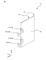
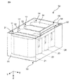
- a perspective view showing a capacitor module according to the first embodiment of the present invention Perspective view of the capacitor module case of FIG. 1 omitted.
- a perspective view showing a capacitor of the capacitor module of FIG. A perspective view showing a capacitor of the capacitor module of FIG. Side view of the capacitor module of FIG.
- a perspective view showing a metal plate of the capacitor module of FIG. A perspective view showing the first bus bar of the capacitor module of FIG.
- Side view of the capacitor module according to the second modification of the first embodiment Perspective view of the capacitor module according to the third modification of the first embodiment.
- Side view of the capacitor module according to the second embodiment Perspective view of the capacitor module according to the modified example of the second embodiment.
- each unit capacitor has a capacitor element and an element electrode plate, and each element electrode plate is connected to one electrode of each capacitor element.
- Each element electrode plate is arranged adjacent to each capacitor, and heat generated from the capacitor element can be dissipated by the element electrode plate.
- the number of element electrode plates may be excessive depending on the arrangement of the capacitor elements. If the number of element electrode plates is excessive, there is a problem that the configuration becomes complicated and the assembly process becomes complicated.
- the present inventors have studied a capacitor module having a simplified configuration while improving heat dissipation, and have reached the following invention.
- the capacitor module according to one aspect of the present invention is A side surface having a pair of flat portions facing each other, a pair of flat portions facing each other, and a pair of curved portions connecting one flat portion and the other flat portion, connecting the first electrode and the second electrode facing each other, and the first electrode and the second electrode.
- a plurality of capacitors arranged in a row so that the flat portions face each other, and With at least one metal plate located between the respective flat portions of the adjacent capacitors and in contact with at least one of the first electrodes of the adjacent capacitors, respectively.
- a second bus bar that is electrically connected to each of the second electrodes, Equipped with Each of the first electrodes of the plurality of capacitors is electrically connected to at least one metal plate.
- the metal plate arranged between the flat portions can cover any first electrode of the plurality of capacitors. Therefore, it is possible to simplify the configuration while improving the heat dissipation by the metal plate.
- the metal plate may be bent in different directions so as to contact the first electrodes of both adjacent capacitors.
- each of the metal plates comes into contact with the two first electrodes. Therefore, it is easy to change the design such as arranging the metal plate in all the spaces between the flat portions or decimating the metal plates. Further, since the specifications of each metal plate can be unified, the metal plates can be mass-produced and the manufacturing cost can be reduced.
- the metal plate has a main body portion arranged between the flat portions of adjacent capacitors, an electrode contact portion extending from the main body portion so as to contact the first electrode, and a main body portion so as to contact the first bus bar.
- the electrode contact portion is one or more first electrode contact portions in contact with the first electrode of one of the adjacent capacitors and one or more second electrode contact portions in contact with the first electrode of the other capacitor. And may be formed alternately at intervals.
- the electrode contact parts can be arranged in a well-balanced manner.
- the bus bar contact portion may be formed at a position where the main body portion extends from between the flat portions of the adjacent capacitors to the curved portions of the adjacent capacitors.
- the distance between the bus bar contact portion and the second electrode can be increased as compared with the case where the bus bar contact portion is provided at a position extended toward the second electrode side. Therefore, it is possible to prevent a short circuit between the bus bar contact portion and the second electrode.
- the bus bar contact portion may be formed so as to be located between the curved portions.
- the bus bar contact portion can be arranged in the dead space between the curved portions. Therefore, it contributes to the miniaturization of the capacitor module.
- the number of the plurality of capacitors is 2n + 1 (n is a natural number), and the number of metal plates may be n + 1 or more and 2n or less.
- each of the first electrodes can be connected to a metal plate arranged between adjacent capacitors while making the number of metal plates smaller than the number of capacitors. Therefore, the configuration can be simplified and the manufacturing cost can be suppressed.
- the number of the plurality of capacitors is 2n (n is a natural number of 2 or more), and the number of metal plates may be n or more and 2n-1 or less.
- each of the first electrodes can be connected to a metal plate arranged between adjacent capacitors while making the number of metal plates smaller than the number of capacitors. Therefore, the configuration can be simplified and the manufacturing cost can be suppressed.
- the number of a plurality of capacitors is m (m is a natural number of 3 or more), and the number of metal plates may be m-1.
- a metal plate can be placed anywhere between the flat portions. Therefore, the heat dissipation of the capacitor module can be improved.
- FIG. 1 is a perspective view showing a capacitor module 1 according to the first embodiment of the present invention.
- FIG. 2 is a perspective view of the capacitor module 1 of FIG. 1 in which the case 91 is omitted.
- 3A and 3B are perspective views showing the capacitor 11 of the capacitor module of FIG.
- FIG. 4 is a side view of the capacitor module 1 of FIG.
- FIG. 5 is a perspective view showing the metal plate 51 of the capacitor module 1 of FIG.
- FIG. 6 is a perspective view showing the first bus bar 54 of the capacitor module 1 of FIG.
- FIG. 7 is a perspective view of the capacitor module 1 of FIG. 1 as viewed from another direction.
- the X, Y, and Z directions in the figure indicate the height direction, the horizontal direction, and the vertical direction of the capacitor module 1, respectively.
- the capacitor module 1 includes four capacitors 11 to 14, three metal plates 51 to 53, a first bus bar 54, and a second bus bar 55.
- the capacitor module 1 four capacitors 11 to 14, a metal plate 51 to 53, a part of the first bus bar 54, and a part of the second bus bar 55 are housed in a case 91 made of resin.
- the inside of the case 91 is filled with a sealing resin (not shown).
- the case 91 has an opening 92 formed at a position facing the bottom surface 93.
- the case 91 is formed of an insulating material, for example, a synthetic resin such as polyphenylene sulfide (PPS resin) or polybutylene terephthalate (PBT resin).
- PPS resin polyphenylene sulfide
- PBT resin polybutylene terephthalate
- the sealing resin is filled inside the case 91 to seal each component of the capacitor module 1.
- the sealing resin is a thermosetting resin, and for example, an epoxy resin can be used. Alternatively, it may be urethane resin.
- Capacitors 11 to 14 are film capacitors formed by winding a dielectric film.
- the capacitors 11 to 14 are formed by winding a dielectric film having a metal vapor deposition film formed on the surface thereof and pressing the wound body of the dielectric film into a flat shape.
- the capacitor module 1 includes four capacitors 11 to 14. Since the capacitors 11 to 14 have the same configuration, the capacitor 11 will be described here.
- the capacitor 11 has a first electrode 21, a second electrode 31, and a side surface 41.
- the first electrode 21 and the second electrode 31 are (end face) electrodes arranged so as to face each other.
- the side surface 41 is a side surface connecting the first electrode 21 and the second electrode 31.
- the side surface 41 has a pair of flat portions 41a facing each other and a pair of curved portions 41b connecting the pair of flat portions 41a to each other.
- the dielectric film of the capacitor 11 for example, a plastic film such as polyethylene terephthalate, polypropylene, polyphenylene sulfide, or polyethylene naphthalate can be used. Further, Al, Zn or the like can be used as the metal vapor deposition film formed on the surface of the plastic film.
- the first electrode 21 and the second electrode 31 are formed by spraying, for example, Zn or the like on the end portion of the wound dielectric film.
- the capacitors 11 to 14 are arranged in a row inside the case 91 so that the flat portions 41a to 44a face each other. That is, the flat portion 41a and the flat portion 42a face each other, the flat portion 42a and the flat portion 43a face each other, and the flat portion 43a and the flat portion 44a face each other. Capacitors 11 to 14 are arranged so that the distance between the flat portions 41a to 44a is about 0.5 mm to 4.0 mm. Further, the capacitors 11 to 14 are arranged so that the curved portions 41b to 44b on one side of the curved portions 41b to 44b face the opening 92 and the curved portions 41b to 44b on the other side face the bottom surface 93.
- the metal plates 51 to 53 are conductive members that electrically connect the first electrodes 21 to 24 of the capacitors 11 to 14 and the first bus bar 54, respectively.
- each of the metal plates 51 to 53 has a main body portion 61 to 63, an electrode contact portion 71 to 73, and a bus bar contact portion 81 to 83, respectively.
- the metal plates 51 to 53 have main bodies 61 to 63 arranged in a space between the flat portions 41a to 44a of the capacitors 11 to 14. That is, the metal plates 51 to 53 are formed between the flat portions 41a and 42a of the adjacent capacitors 11 and 12, between the flat portions 42a and 43a of the adjacent capacitors, and the flat portions of the adjacent capacitors 13 and 14, respectively. It is arranged between the portions 43a and 44a.
- the main body portion 61 of the metal plate 51 is arranged in the space S1 between the flat portion 41a and the flat portion 42a.
- the main body portion 62 of the metal plate 52 is arranged in the space S2 between the flat portion 42a and the flat portion 43a.
- the main body portion 63 of the metal plate 53 is arranged in the space S3 between the flat portion 43a and the flat portion 44a. That is, in the capacitor module 1, three metal plates 51 to 53 are arranged with respect to the four capacitors 11 to 14.
- the main body 61 of the metal plate 51 is a portion arranged in the space S1 between the flat portion 41a and the flat portion 42a.
- the space S1 is also filled with the sealing resin.
- the sealing resin enters between the main body portion 61 and the flat portion 41a and between the main body portion 61 and the flat portion 42a, the thermal conductivity is improved.
- the metal plate 51 is provided with an electrode contact portion 71 extending from the main body portion 61 so as to come into contact with the first electrodes 21 and 22.
- the electrode contact portion 71 is configured by bending a part of the end portion of the main body portion 61 in the vertical direction (Z direction) in the horizontal direction (Y direction).
- four electrode contact portions 71 are provided.
- the electrode contact portion 71a is bent so as to come into contact with the first electrode 21 of the capacitor 11 from the main body portion 61.
- the electrode contact portion 71b is bent so as to come into contact with the first electrode 22 of the capacitor 12 from the main body portion 61. That is, the electrode contact portion 71a and the electrode contact portion 71b are bent in different directions so that the metal plate 51 comes into contact with the first electrodes 21 and 22 of both the capacitors 11 and 12.
- they are alternately provided at intervals in the height direction (X direction).
- the electrode contact portions 71a and the electrode contact portions 71b By alternately providing the electrode contact portions 71a and the electrode contact portions 71b, the electrode contact portions 71 can be arranged in a well-balanced manner. Further, the electrode contact portion 71a and the electrode contact portion 71b can be evenly contacted with the first electrode 21 and the first electrode 22.
- the arrangement of the electrode contact portion 71a and the electrode contact portion 71b is not limited to this, and any configuration may be used as long as it can be connected to both the first electrode 21 of the capacitor 11 and the first electrode 22 of the capacitor 12.
- the electrode contact portion 71 is electrically connected to the first electrodes 21 and 22 by soldering. It is not necessary to solder all the electrode contact portions 71. For example, one of each of the two electrode contact portions 71a and one of the electrode contact portions 71b may be soldered, and the rest may be simply contacted with the first electrodes 21 and 22 without soldering. By appropriately selecting the electrode contact portion 71 to be soldered, it is possible to reduce the influence of heat on the characteristics of the capacitor module 1 at the time of soldering. By soldering all the electrode contact portions 71 and the first electrodes 21 and 22, the connection reliability between the metal plate 51 and the first electrodes 21 and 22 can be improved.
- the metal plate 51 is provided with a bus bar contact portion 81 extending from the main body portion 61 so as to come into contact with the first bus bar 54.
- the bus bar contact portion 81 is a portion to be inserted into a hole 64a (see FIG. 6) provided in the buried portion 64 of the first bus bar 54, which will be described later.
- the bus bar contact portion 81 is configured as a protruding portion in which a part of the end portion of the main body portion 61 in the X direction is further projected in the X direction.
- the bus bar contact portion 81 is located at a position where the main body portion 61 extends from the space S1 between the flat portions 41a and 42a toward the space S4 between the curved portions 41b and 42b. It is formed. That is, the bus bar contact portion 81 extends from between the flat portions 41a and 42a of the adjacent capacitors 11 and 12 to between the curved portions 41b and 52b of the capacitors 11 and 12, respectively. Is formed in. Similarly, the bus bar contact portion 82 is formed at a position where the main body portion 62 extends from the space S2 toward the space S5, and the bus bar contact portion 83 is formed at a position where the main body portion 63 extends from the space S3 toward the space S6. It is formed. The bus bar contact portions 81 to 83 are electrically connected to the first bus bar 54 by soldering.
- the metal plates 51 to 53 can be formed by, for example, pressing a metal plate having a thickness of about 0.3 mm to 0.5 mm.
- the metal plates 51 to 53 are made of a metal thinner than the first bus bar 54 described later. Since it is formed of a thin metal having a lower cost than the first bus bar 54, the manufacturing cost can be reduced by connecting the first electrodes 21 to 24 of the capacitors 11 to 14 to the first bus bar 54 via the metal plates 51 to 53. Can be reduced.
- the four capacitors 11 to 14 are arranged in a row, three spaces S1 to S3 are formed between the flat portions.
- one metal plate 51 to 53 is arranged in each of the three spaces S1 to S3.
- the heat dissipation of the capacitor module 1 can be improved.
- the first electrodes 21 to 24 of the capacitors 11 to 14 and the first bus bar 54 are used by using the metal plates 51 to 53 which are smaller than the number of the capacitors 11 to 14.
- Can be connected, and the configuration of the capacitor module 1 can be simplified.
- the metal plates 51 to 53 in the spaces S1 to S3, respectively the current flowing through the metal plates 51 to 53 can efficiently cancel the magnetic field due to the current flowing through the capacitors 11 to 14, and the capacitor module 1 is low. ESL can be planned.
- the spaces S1 to S3 between the flat portions are filled with a sealing resin.
- the heat generated from the capacitors 11 to 14 is conducted to the metal plates 51 to 53 through the sealing resin. Since the metal plates 51 to 53 are electrically and mechanically connected to the first bus bar 54, the heat of the capacitors 11 to 14 is efficiently transferred from the exposed portion 74 of the first bus bar 54 exposed to the outside of the sealing resin. The heat can be dissipated to the outside of the capacitor module 1.
- the metal plate 51 is in contact with any of the first electrodes 21 and 22 of the capacitors 11 and 12, respectively.
- the metal plate 52 contacts any of the first electrodes 22 and 23 of the capacitors 12 and 13, respectively, and the metal plate 53 touches any of the first electrodes 23 and 24 of the capacitors 13 and 14, respectively.
- the first electrode 21 of the capacitor 11 is in contact with the metal plate 51
- the first electrode 22 of the capacitor 12 is in contact with the metal plate 51 and the metal plate 52
- the first electrode 23 of the capacitor 13 is in contact with the metal plate 52.
- the first electrode 24 of the capacitor 14 comes into contact with the metal plate 53. That is, among the capacitors 11 to 14, the capacitors 12 and 13 arranged inside are in contact with two metal plates, respectively, and the capacitors 11 and 14 arranged outside are in contact with one metal plate, respectively.
- the present embodiment as shown in FIGS. 2 and 4, three metal plates 51 to 53 are arranged for the four capacitors 11 to 14.
- the capacitors 11 to 14 are arranged in a row so that the flat portions 41a to 44a face each other, the number of spaces S1 to S3 between the flat portions becomes three.
- the number of metal plates 51 to 53 are arranged in all the spaces S1 to S3, when the number of capacitors is 4, the number of metal plates is 3. That is, the number of metal plates is at most one less than the number of capacitors.
- the first bus bar 54 is a plate-shaped conductive member that is electrically connected to the first electrodes 21 to 24 of the capacitors 11 to 14.
- the first bus bar 54 is formed of a conductive member having a thickness of about 0.3 mm to 2 mm. As shown in FIG. 2, the first bus bar 54 and the respective first electrodes 21 to 24 are electrically connected to each other via the metal plates 51 to 53.
- the first bus bar 54 has three buried portions 64 and an exposed portion 74.
- the buried portion 64 is a portion connected to the bus bar contact portions 81 to 83 of the metal plates 51 to 53, and is embedded inside the sealing resin in the case 91.
- the exposed portion 74 is a portion exposed to the outside of the case 91.
- holes 64a are formed in each of the buried portions 64.
- the bus bar contact portions 81 to 83 of the metal plates 51 to 53 are inserted into the holes 64a and soldered to electrically connect the first bus bar 54 and the metal plates 51 to 53.
- the connection between the first bus bar 54 and the metal plates 51 to 53 is not limited to soldering, and can be performed by, for example, welding or a mechanical method such as caulking.
- the buried portion 64 of the first bus bar 54 is arranged at a position higher than the capacitors 11 to 14 in the height direction (X direction). Specifically, the buried portion 64 is arranged at a position closer to the opening 92 than the position H1 at the top of the curved portions 41b to 44b arranged toward the opening 92 of the capacitors 11 to 14. By arranging the buried portion 64 at this position, the metal plates 51 to 53 and the first bus bar 54 can be connected at a position away from the second electrodes 31 to 34. Therefore, it is possible to prevent a short circuit between the first bus bar 54 and the second electrodes 31 to 34.
- the second bus bar 55 is a plate-shaped conductive member electrically connected to the second electrodes 31 to 34 of the capacitors 11 to 14.
- the second bus bar 55 is formed of a conductive member having a thickness of about 0.3 mm to 2 mm.
- the second bus bar 55 has an exposed portion 65 exposed to the outside of the case 91, and an electrode contact portion 75 in contact with the second electrodes 31 to 34.
- the second bus bar 55 and the second electrodes 31 to 34 are electrically connected by soldering.
- the exposed portion 74 of the first bus bar 54 and the exposed portion 65 of the second bus bar 55 are arranged with a gap V1 of about 0.5 mm.
- V1 the distance between the exposed portion 74 of the first bus bar 54 and the exposed portion 65 of the second bus bar 55 to some extent, it is possible to reduce the ESL of the capacitor module 1. Therefore, it is preferable to arrange the exposed portion 74 and the exposed portion 65 so that the size of the interval V1 is about 0.5 mm.
- the capacitor module 1 includes four capacitors 11 to 14, three metal plates 51 to 53, a first bus bar 54, and a second bus bar 55.
- the capacitors 11 to 13 have first electrodes 21 to 24, second electrodes 31 to 34, and side surfaces 41 to 44, respectively.
- the first electrodes 21 to 24 and the second electrodes 31 to 34 are arranged so as to face each other.
- the side surfaces 41 to 44 connect the first electrodes 21 to 24 and the second electrodes 31 to 34, and have a pair of flat portions 41a to 44a facing each other, one flat portion 41a to 44a, and the other flat portions 41a to 44a. It has a pair of curved portions 41b to 44b that connect the above.
- the capacitors 11 to 14 are arranged in a row so that the flat portions 41a to 44a face each other.
- the metal plates 51 to 53 are arranged between the flat portions 41a to 44a of the adjacent capacitors 11 to 14, and are in contact with at least one of the first electrodes 21 to 24 of the adjacent capacitors 11 to 14, respectively.
- the first bus bar 54 is electrically connected to the metal plates 51 to 53.
- the second bus bar 55 is electrically connected to each of the second electrodes 31 to 34.
- the first electrodes 21 to 24 of the capacitors 11 to 14 are electrically connected to the metal plates 51 to 53, respectively.
- the metal plates 51 to 53 arranged between the flat portions 41a to 44a can cover any of the first electrodes 21 to 24 of the capacitors 11 to 14. Therefore, the metal plates 51 to 53 can improve the heat dissipation of the capacitor module 1 and simplify the configuration of the capacitor module 1.
- the metal plates 51 to 53 in the spaces S1 to S3, the magnetic field of the current flowing inside the capacitors 11 to 14 can be efficiently canceled, and the low ESL of the capacitor module 1 can be achieved.
- the metal plates 51 to 53 are bent in different directions so as to come into contact with the first electrodes 21 to 24 of both of the two adjacent capacitors 11 to 14.
- each of the metal plates 51 to 53 comes into contact with the first electrodes 21 to 24 of the two capacitors 11 to 14. Therefore, it is easy to change the design such as arranging a metal plate in all of the spaces S1 to S3 between the flat portions 41a to 44a, arranging the metal plate by thinning out, and the like. Further, by unifying the specifications of the metal plates 51 to 53, mass production of the metal plates 51 to 53 becomes possible, and the manufacturing cost can be suppressed.
- the metal plates 51 to 53 have a main body portion 61 to 63, an electrode contact portion 71 to 73, and a bus bar contact portion 81 to 83.
- the main body portions 61 to 63 are arranged between the flat portions 41a to 44a of the adjacent capacitors 11 to 14.
- the electrode contact portions 71 to 73 extend from the main body portions 61 to 63 so as to be in contact with the first electrodes 21 to 24.
- the bus bar contact portions 81 to 83 extend from the main body portions 61 to 63 so as to be in contact with the first bus bar 54, and are between the flat portions 41a to 44a (spaces S1 to S3) and between the curved portions 41b to 44b (space S4).
- the main body portions 61 to 63 are formed at positions extending toward S6).
- the metal plates 51 to 53 and the first bus bar 54 can be connected at a position away from the second electrodes 31 to 34. Therefore, it is possible to prevent a short circuit between the first bus bar 54 and the second electrodes 31 to 34.
- the number of capacitors 11 to 14 is m (m is a natural number of 3 or more), and the number of metal plates 51 to 53 is m-1. In the present embodiment, the number of capacitors 11 to 14 is 4, and the number of metal plates 51 to 53 is 3.
- the metal plates 51 to 53 can be arranged in any of the spaces S1 to S3 between the flat portions 41a to 44a. Therefore, it is possible to improve the heat dissipation of the capacitor module 1 while simplifying the configuration.
- the present invention is not limited to this.
- the three buried portions 64 of the first bus bar 54 do not necessarily have to be arranged at the same position in the height direction (X direction). Even when the positions in the height direction are different, the same effect as that of the first embodiment can be obtained.
- FIG. 8 is a perspective view of the capacitor module 1a according to the first modification of the first embodiment. As shown in FIG. 8, the capacitors 11 to 14 may be arranged so that the first electrodes 21 to 24 are arranged toward the bottom surface 93 and the second electrodes 31 to 34 are arranged toward the opening 92. ..
- FIG. 9 is a side view of the capacitor module 1b according to the second modification of the first embodiment.
- the buried portion 64b of the first bus bar 54b may be arranged at a position lower than the position H1 at the top of the curved portions 41b to 44b of the capacitors 11 to 14. That is, the buried portion 64b of the first bus bar 54b is arranged in each of the spaces S4 to S6 between the curved portions 41b to 44b.
- the dead space can be effectively utilized by locating the buried portion 64b at this position. Therefore, it contributes to the miniaturization of the capacitor module 1b.
- FIG. 10 is a perspective view of the capacitor module 1c according to the third modification of the first embodiment.
- the first bus bar 54c is provided with a cooling portion 76 extending from the exposed portion 74c, and the cooling portion 76 is provided with a thermal pad 77.
- the first bus bar 54c can be cooled in a larger area, so that the heat dissipation of the capacitor module 1c can be further improved.
- a thermal pad may be arranged on the first bus bar 54 of the capacitor module 1 of the first embodiment.
- the first bus bar 54 can be cooled by arranging the thermal pad on the exposed portion 74 of the first bus bar 54. Thereby, the heat dissipation effect of the capacitor module 1 can be further improved.
- FIG. 11 is an enlarged view of a part of the first bus bar 54d according to the modified example 4 of the first embodiment. As shown in FIG. 11, a recess 66 may be provided in a part of the buried portion 64d of the first bus bar 54d. By providing the recess 66 in the vicinity of the hole 64a into which the bus bar contact portion 83 of the metal plate 53 is inserted, it is possible to suppress heat escape during soldering.
- the second embodiment mainly describes the differences from the first embodiment.
- the same or equivalent configurations as those in the first embodiment will be described with the same reference numerals. Further, in the second embodiment, the description overlapping with the first embodiment is omitted.
- FIG. 12 is a side view of the capacitor module 2 according to the second embodiment.
- the number of metal plates 151 to 152 is different from that of the first embodiment. Specifically, of the spaces S1 to S3 between the flat portions, the metal plate 151 is arranged in the space S1, and the metal plate 152 is arranged in the space S3.
- the metal plates 151 and 152 can be connected to the first electrodes of two adjacent capacitors, respectively. Therefore, the metal plates 151 to 152 may be arranged so that any of the metal plates 151 to 152 is connected to all the first electrodes 21 to 24 without arranging them in all the spaces S1 to S3. ..
- the electrode contact portion 171a of the metal plate 151 is connected to the first electrode 21 of the capacitor 11, and the electrode contact portion 171b is connected to the first electrode 22 of the capacitor 12.
- the electrode contact portion 172a of the metal plate 152 is connected to the first electrode 23 of the capacitor 13, and the electrode contact portion 172b is connected to the first electrode 24 of the capacitor 14.
- the number of capacitors is an odd number, that is, when the number of capacitors is 2n + 1 (n is a natural number), the minimum number of metal plates is n + 1, and the maximum number of metal plates is 2n.
- n 2
- the number of a plurality of capacitors is 2n + 1 (n is a natural number), and the number of metal plates is n + 1 or more and 2n or less.
- the number of a plurality of capacitors is 2n (n is a natural number of 2 or more), and the number of metal plates is n or more and 2n-1 or less.
- the configuration of the capacitor module 2 can be simplified.
- FIG. 13 is a perspective view of the capacitor module 2a according to the modified example of the second embodiment. In FIG. 13, the case 91 and the capacitor 14 are omitted.
- the lengths of the metal plates 51a and 52a in the vertical direction (Z direction) are formed shorter than those of the metal plates 51 to 53 of the first embodiment.
- the vertical length of the metal plates 51a and 62a may be shortened to about 1 ⁇ 2 of the vertical length of the capacitors 11 to 14.
- the metal plates 51a and 52a can be arranged in the central portion of the capacitors 11 to 13, which are the portions that generate the most heat due to the ripple current flowing through the capacitors 11 to 13.
- the heat dissipation effect can be improved.
- the shapes of the first bus bar 154a and the second bus bar 155a may be different. Specifically, as shown in FIG. 13, the exposed portion 174a of the first bus bar 154a and the exposed portion 165a of the second bus bar 155a are formed so as to extend in the height direction (X direction). Even if the first bus bar 154a and the second bus bar 155a are arranged in this way, the same effect as that of the first embodiment can be obtained.
- the present invention is useful for capacitors used in various electronic devices, electrical devices, industrial devices, vehicle devices, and the like.
Landscapes
- Engineering & Computer Science (AREA)
- Power Engineering (AREA)
- Microelectronics & Electronic Packaging (AREA)
- Manufacturing & Machinery (AREA)
- Fixed Capacitors And Capacitor Manufacturing Machines (AREA)
- Inverter Devices (AREA)
Priority Applications (3)
| Application Number | Priority Date | Filing Date | Title |
|---|---|---|---|
| CN202190000473.5U CN219143983U (zh) | 2020-05-28 | 2021-05-18 | 电容器模块 |
| JP2022526915A JP7452640B2 (ja) | 2020-05-28 | 2021-05-18 | コンデンサモジュール |
| US17/994,042 US12387881B2 (en) | 2020-05-28 | 2022-11-25 | Capacitor module having a metal sheet between adjacent capacitors |
Applications Claiming Priority (2)
| Application Number | Priority Date | Filing Date | Title |
|---|---|---|---|
| JP2020-093502 | 2020-05-28 | ||
| JP2020093502 | 2020-05-28 |
Related Child Applications (1)
| Application Number | Title | Priority Date | Filing Date |
|---|---|---|---|
| US17/994,042 Continuation US12387881B2 (en) | 2020-05-28 | 2022-11-25 | Capacitor module having a metal sheet between adjacent capacitors |
Publications (1)
| Publication Number | Publication Date |
|---|---|
| WO2021241320A1 true WO2021241320A1 (ja) | 2021-12-02 |
Family
ID=78744652
Family Applications (1)
| Application Number | Title | Priority Date | Filing Date |
|---|---|---|---|
| PCT/JP2021/018752 Ceased WO2021241320A1 (ja) | 2020-05-28 | 2021-05-18 | コンデンサモジュール |
Country Status (4)
| Country | Link |
|---|---|
| US (1) | US12387881B2 (https=) |
| JP (1) | JP7452640B2 (https=) |
| CN (1) | CN219143983U (https=) |
| WO (1) | WO2021241320A1 (https=) |
Cited By (5)
| Publication number | Priority date | Publication date | Assignee | Title |
|---|---|---|---|---|
| JP2023090425A (ja) * | 2021-12-17 | 2023-06-29 | 株式会社指月電機製作所 | コンデンサ |
| WO2024171701A1 (ja) * | 2023-02-15 | 2024-08-22 | パナソニックIpマネジメント株式会社 | コンデンサ |
| WO2025126705A1 (ja) * | 2023-12-12 | 2025-06-19 | 株式会社村田製作所 | コンデンサモジュール |
| WO2026009620A1 (ja) * | 2024-07-01 | 2026-01-08 | 株式会社デンソー | コンデンサモジュール |
| WO2026063087A1 (ja) * | 2024-09-18 | 2026-03-26 | 株式会社村田製作所 | コンデンサモジュール |
Families Citing this family (1)
| Publication number | Priority date | Publication date | Assignee | Title |
|---|---|---|---|---|
| FR3158583B1 (fr) * | 2024-01-24 | 2025-12-26 | Valeo Eautomotive Germany Gmbh | Condensateur pour bus continu d’un onduleur |
Citations (4)
| Publication number | Priority date | Publication date | Assignee | Title |
|---|---|---|---|---|
| JPH01176919U (https=) * | 1988-06-02 | 1989-12-18 | ||
| JPH09260180A (ja) * | 1996-03-19 | 1997-10-03 | Shizuki Denki Seisakusho:Kk | 低インダクタンスコンデンサ |
| WO2016002177A1 (ja) * | 2014-07-02 | 2016-01-07 | パナソニックIpマネジメント株式会社 | フィルムコンデンサ |
| JP2020088064A (ja) * | 2018-11-20 | 2020-06-04 | ルビコン電子株式会社 | コンデンサモジュール |
Family Cites Families (5)
| Publication number | Priority date | Publication date | Assignee | Title |
|---|---|---|---|---|
| JP2009289967A (ja) * | 2008-05-29 | 2009-12-10 | Hitachi Aic Inc | フィルムコンデンサユニット |
| JP2013251351A (ja) * | 2012-05-31 | 2013-12-12 | Meidensha Corp | コンデンサ |
| JP5989533B2 (ja) | 2012-12-07 | 2016-09-07 | 株式会社指月電機製作所 | コンデンサ |
| JP6347768B2 (ja) * | 2015-01-22 | 2018-06-27 | カルソニックカンセイ株式会社 | コンデンサ構造 |
| DE102016223256A1 (de) * | 2016-11-24 | 2018-05-24 | Robert Bosch Gmbh | Kondensator, insbesondere Zwischenkreiskondensator für ein Mehrphasensystem |
-
2021
- 2021-05-18 JP JP2022526915A patent/JP7452640B2/ja active Active
- 2021-05-18 WO PCT/JP2021/018752 patent/WO2021241320A1/ja not_active Ceased
- 2021-05-18 CN CN202190000473.5U patent/CN219143983U/zh active Active
-
2022
- 2022-11-25 US US17/994,042 patent/US12387881B2/en active Active
Patent Citations (4)
| Publication number | Priority date | Publication date | Assignee | Title |
|---|---|---|---|---|
| JPH01176919U (https=) * | 1988-06-02 | 1989-12-18 | ||
| JPH09260180A (ja) * | 1996-03-19 | 1997-10-03 | Shizuki Denki Seisakusho:Kk | 低インダクタンスコンデンサ |
| WO2016002177A1 (ja) * | 2014-07-02 | 2016-01-07 | パナソニックIpマネジメント株式会社 | フィルムコンデンサ |
| JP2020088064A (ja) * | 2018-11-20 | 2020-06-04 | ルビコン電子株式会社 | コンデンサモジュール |
Cited By (6)
| Publication number | Priority date | Publication date | Assignee | Title |
|---|---|---|---|---|
| JP2023090425A (ja) * | 2021-12-17 | 2023-06-29 | 株式会社指月電機製作所 | コンデンサ |
| JP7802519B2 (ja) | 2021-12-17 | 2026-01-20 | 株式会社指月電機製作所 | コンデンサ |
| WO2024171701A1 (ja) * | 2023-02-15 | 2024-08-22 | パナソニックIpマネジメント株式会社 | コンデンサ |
| WO2025126705A1 (ja) * | 2023-12-12 | 2025-06-19 | 株式会社村田製作所 | コンデンサモジュール |
| WO2026009620A1 (ja) * | 2024-07-01 | 2026-01-08 | 株式会社デンソー | コンデンサモジュール |
| WO2026063087A1 (ja) * | 2024-09-18 | 2026-03-26 | 株式会社村田製作所 | コンデンサモジュール |
Also Published As
| Publication number | Publication date |
|---|---|
| US20230089940A1 (en) | 2023-03-23 |
| JP7452640B2 (ja) | 2024-03-19 |
| JPWO2021241320A1 (https=) | 2021-12-02 |
| US12387881B2 (en) | 2025-08-12 |
| CN219143983U (zh) | 2023-06-06 |
Similar Documents
| Publication | Publication Date | Title |
|---|---|---|
| JP7452640B2 (ja) | コンデンサモジュール | |
| US8416556B2 (en) | Power capacitor | |
| JP4823116B2 (ja) | 半導体モジュール | |
| CN115332732B (zh) | 汇流条模块 | |
| CN115332731B (zh) | 汇流条模块 | |
| JP6305731B2 (ja) | ケースモールド型コンデンサおよびその製造方法 | |
| US10958055B2 (en) | Circuit assembly and electrical junction box | |
| JP2011155138A (ja) | コンデンサ | |
| JP7213408B2 (ja) | コンデンサ | |
| CN115485797A (zh) | 电容器模块 | |
| JP2019216173A (ja) | コンデンサ | |
| US12477694B2 (en) | Circuit device | |
| JP2008270329A (ja) | コンデンサ | |
| JP2025092766A (ja) | 電力変換装置 | |
| US12340943B2 (en) | Electronic device | |
| CN112951605A (zh) | 具有低电感连接特征的电容器和电子模块组件 | |
| JP2024056186A (ja) | コンデンサ | |
| WO2023276533A1 (ja) | コンデンサモジュール | |
| JP7700840B2 (ja) | コンデンサモジュール | |
| JP2016066666A (ja) | コンデンサ | |
| JP2025111219A (ja) | コンデンサモジュール | |
| JP2025187209A (ja) | 金属化フィルムコンデンサ | |
| JP2025134280A (ja) | タブリード付き基板及び電池モジュール | |
| JP2023008578A (ja) | コンデンサ | |
| JP2002217058A (ja) | コンデンサ装置およびコンデンサモジュール |
Legal Events
| Date | Code | Title | Description |
|---|---|---|---|
| 121 | Ep: the epo has been informed by wipo that ep was designated in this application |
Ref document number: 21813664 Country of ref document: EP Kind code of ref document: A1 |
|
| ENP | Entry into the national phase |
Ref document number: 2022526915 Country of ref document: JP Kind code of ref document: A |
|
| NENP | Non-entry into the national phase |
Ref country code: DE |
|
| 122 | Ep: pct application non-entry in european phase |
Ref document number: 21813664 Country of ref document: EP Kind code of ref document: A1 |