WO2021241320A1 - Capacitor module - Google Patents
Capacitor module Download PDFInfo
- Publication number
- WO2021241320A1 WO2021241320A1 PCT/JP2021/018752 JP2021018752W WO2021241320A1 WO 2021241320 A1 WO2021241320 A1 WO 2021241320A1 JP 2021018752 W JP2021018752 W JP 2021018752W WO 2021241320 A1 WO2021241320 A1 WO 2021241320A1
- Authority
- WO
- WIPO (PCT)
- Prior art keywords
- capacitors
- electrode
- bus bar
- capacitor module
- contact
- Prior art date
Links
- 239000003990 capacitor Substances 0.000 title claims abstract description 226
- 239000002184 metal Substances 0.000 claims abstract description 138
- 229910052751 metal Inorganic materials 0.000 claims abstract description 138
- 230000017525 heat dissipation Effects 0.000 abstract description 13
- 229920005989 resin Polymers 0.000 description 14
- 239000011347 resin Substances 0.000 description 14
- 230000004048 modification Effects 0.000 description 12
- 238000012986 modification Methods 0.000 description 12
- 238000007789 sealing Methods 0.000 description 10
- 230000000694 effects Effects 0.000 description 9
- 238000005476 soldering Methods 0.000 description 8
- 238000004519 manufacturing process Methods 0.000 description 6
- -1 polybutylene terephthalate Polymers 0.000 description 4
- 239000004734 Polyphenylene sulfide Substances 0.000 description 3
- 238000001816 cooling Methods 0.000 description 3
- 229920000069 polyphenylene sulfide Polymers 0.000 description 3
- 239000002985 plastic film Substances 0.000 description 2
- 229920006255 plastic film Polymers 0.000 description 2
- 229920001707 polybutylene terephthalate Polymers 0.000 description 2
- 238000003825 pressing Methods 0.000 description 2
- 238000007740 vapor deposition Methods 0.000 description 2
- 238000004804 winding Methods 0.000 description 2
- 239000004743 Polypropylene Substances 0.000 description 1
- 238000005452 bending Methods 0.000 description 1
- 239000003822 epoxy resin Substances 0.000 description 1
- 239000011810 insulating material Substances 0.000 description 1
- 238000010297 mechanical methods and process Methods 0.000 description 1
- 238000000034 method Methods 0.000 description 1
- 229920003207 poly(ethylene-2,6-naphthalate) Polymers 0.000 description 1
- 229920000647 polyepoxide Polymers 0.000 description 1
- 239000011112 polyethylene naphthalate Substances 0.000 description 1
- 229920000139 polyethylene terephthalate Polymers 0.000 description 1
- 239000005020 polyethylene terephthalate Substances 0.000 description 1
- 229920001155 polypropylene Polymers 0.000 description 1
- 229910000679 solder Inorganic materials 0.000 description 1
- 238000005507 spraying Methods 0.000 description 1
- 229920003002 synthetic resin Polymers 0.000 description 1
- 239000000057 synthetic resin Substances 0.000 description 1
- 229920002803 thermoplastic polyurethane Polymers 0.000 description 1
- 229920001187 thermosetting polymer Polymers 0.000 description 1
- 238000003466 welding Methods 0.000 description 1
- 229910052725 zinc Inorganic materials 0.000 description 1
Images


Classifications
-
- H—ELECTRICITY
- H01—ELECTRIC ELEMENTS
- H01G—CAPACITORS; CAPACITORS, RECTIFIERS, DETECTORS, SWITCHING DEVICES, LIGHT-SENSITIVE OR TEMPERATURE-SENSITIVE DEVICES OF THE ELECTROLYTIC TYPE
- H01G4/00—Fixed capacitors; Processes of their manufacture
- H01G4/38—Multiple capacitors, i.e. structural combinations of fixed capacitors
-
- H—ELECTRICITY
- H01—ELECTRIC ELEMENTS
- H01G—CAPACITORS; CAPACITORS, RECTIFIERS, DETECTORS, SWITCHING DEVICES, LIGHT-SENSITIVE OR TEMPERATURE-SENSITIVE DEVICES OF THE ELECTROLYTIC TYPE
- H01G2/00—Details of capacitors not covered by a single one of groups H01G4/00-H01G11/00
- H01G2/10—Housing; Encapsulation
- H01G2/106—Fixing the capacitor in a housing
-
- H—ELECTRICITY
- H01—ELECTRIC ELEMENTS
- H01G—CAPACITORS; CAPACITORS, RECTIFIERS, DETECTORS, SWITCHING DEVICES, LIGHT-SENSITIVE OR TEMPERATURE-SENSITIVE DEVICES OF THE ELECTROLYTIC TYPE
- H01G2/00—Details of capacitors not covered by a single one of groups H01G4/00-H01G11/00
- H01G2/02—Mountings
- H01G2/04—Mountings specially adapted for mounting on a chassis
-
- H—ELECTRICITY
- H01—ELECTRIC ELEMENTS
- H01G—CAPACITORS; CAPACITORS, RECTIFIERS, DETECTORS, SWITCHING DEVICES, LIGHT-SENSITIVE OR TEMPERATURE-SENSITIVE DEVICES OF THE ELECTROLYTIC TYPE
- H01G4/00—Fixed capacitors; Processes of their manufacture
- H01G4/002—Details
- H01G4/228—Terminals
-
- H—ELECTRICITY
- H01—ELECTRIC ELEMENTS
- H01G—CAPACITORS; CAPACITORS, RECTIFIERS, DETECTORS, SWITCHING DEVICES, LIGHT-SENSITIVE OR TEMPERATURE-SENSITIVE DEVICES OF THE ELECTROLYTIC TYPE
- H01G4/00—Fixed capacitors; Processes of their manufacture
- H01G4/38—Multiple capacitors, i.e. structural combinations of fixed capacitors
- H01G4/385—Single unit multiple capacitors, e.g. dual capacitor in one coil
-
- H—ELECTRICITY
- H01—ELECTRIC ELEMENTS
- H01G—CAPACITORS; CAPACITORS, RECTIFIERS, DETECTORS, SWITCHING DEVICES, LIGHT-SENSITIVE OR TEMPERATURE-SENSITIVE DEVICES OF THE ELECTROLYTIC TYPE
- H01G4/00—Fixed capacitors; Processes of their manufacture
- H01G4/40—Structural combinations of fixed capacitors with other electric elements, the structure mainly consisting of a capacitor, e.g. RC combinations
-
- H—ELECTRICITY
- H01—ELECTRIC ELEMENTS
- H01G—CAPACITORS; CAPACITORS, RECTIFIERS, DETECTORS, SWITCHING DEVICES, LIGHT-SENSITIVE OR TEMPERATURE-SENSITIVE DEVICES OF THE ELECTROLYTIC TYPE
- H01G4/00—Fixed capacitors; Processes of their manufacture
- H01G4/32—Wound capacitors
Definitions
- the present invention relates to a capacitor module.
- Patent Document 1 discloses a configuration in which one electrode of each unit capacitor is connected to a different element electrode plate in a capacitor having a plurality of unit capacitors.
- Patent Document 1 still has room for improvement in terms of achieving both heat dissipation and simplification of the configuration.
- an object of the present invention is to provide a capacitor module having a simplified configuration while improving heat dissipation.
- the capacitor module according to one aspect of the present invention is A side surface having a pair of flat portions facing each other, a pair of flat portions facing each other, and a pair of curved portions connecting one flat portion and the other flat portion, connecting the first electrode and the second electrode facing each other, and the first electrode and the second electrode.
- a plurality of capacitors arranged in a row so that the flat portions face each other, and With at least one metal plate located between the respective flat portions of the adjacent capacitors and in contact with at least one of the first electrodes of the adjacent capacitors, respectively.
- a second bus bar that is electrically connected to each of the second electrodes, Equipped with Each of the first electrodes of the plurality of capacitors is electrically connected to at least one metal plate.
- a perspective view showing a capacitor module according to the first embodiment of the present invention Perspective view of the capacitor module case of FIG. 1 omitted.
- a perspective view showing a capacitor of the capacitor module of FIG. A perspective view showing a capacitor of the capacitor module of FIG. Side view of the capacitor module of FIG.
- a perspective view showing a metal plate of the capacitor module of FIG. A perspective view showing the first bus bar of the capacitor module of FIG.
- Side view of the capacitor module according to the second modification of the first embodiment Perspective view of the capacitor module according to the third modification of the first embodiment.
- Side view of the capacitor module according to the second embodiment Perspective view of the capacitor module according to the modified example of the second embodiment.
- each unit capacitor has a capacitor element and an element electrode plate, and each element electrode plate is connected to one electrode of each capacitor element.
- Each element electrode plate is arranged adjacent to each capacitor, and heat generated from the capacitor element can be dissipated by the element electrode plate.
- the number of element electrode plates may be excessive depending on the arrangement of the capacitor elements. If the number of element electrode plates is excessive, there is a problem that the configuration becomes complicated and the assembly process becomes complicated.
- the present inventors have studied a capacitor module having a simplified configuration while improving heat dissipation, and have reached the following invention.
- the capacitor module according to one aspect of the present invention is A side surface having a pair of flat portions facing each other, a pair of flat portions facing each other, and a pair of curved portions connecting one flat portion and the other flat portion, connecting the first electrode and the second electrode facing each other, and the first electrode and the second electrode.
- a plurality of capacitors arranged in a row so that the flat portions face each other, and With at least one metal plate located between the respective flat portions of the adjacent capacitors and in contact with at least one of the first electrodes of the adjacent capacitors, respectively.
- a second bus bar that is electrically connected to each of the second electrodes, Equipped with Each of the first electrodes of the plurality of capacitors is electrically connected to at least one metal plate.
- the metal plate arranged between the flat portions can cover any first electrode of the plurality of capacitors. Therefore, it is possible to simplify the configuration while improving the heat dissipation by the metal plate.
- the metal plate may be bent in different directions so as to contact the first electrodes of both adjacent capacitors.
- each of the metal plates comes into contact with the two first electrodes. Therefore, it is easy to change the design such as arranging the metal plate in all the spaces between the flat portions or decimating the metal plates. Further, since the specifications of each metal plate can be unified, the metal plates can be mass-produced and the manufacturing cost can be reduced.
- the metal plate has a main body portion arranged between the flat portions of adjacent capacitors, an electrode contact portion extending from the main body portion so as to contact the first electrode, and a main body portion so as to contact the first bus bar.
- the electrode contact portion is one or more first electrode contact portions in contact with the first electrode of one of the adjacent capacitors and one or more second electrode contact portions in contact with the first electrode of the other capacitor. And may be formed alternately at intervals.
- the electrode contact parts can be arranged in a well-balanced manner.
- the bus bar contact portion may be formed at a position where the main body portion extends from between the flat portions of the adjacent capacitors to the curved portions of the adjacent capacitors.
- the distance between the bus bar contact portion and the second electrode can be increased as compared with the case where the bus bar contact portion is provided at a position extended toward the second electrode side. Therefore, it is possible to prevent a short circuit between the bus bar contact portion and the second electrode.
- the bus bar contact portion may be formed so as to be located between the curved portions.
- the bus bar contact portion can be arranged in the dead space between the curved portions. Therefore, it contributes to the miniaturization of the capacitor module.
- the number of the plurality of capacitors is 2n + 1 (n is a natural number), and the number of metal plates may be n + 1 or more and 2n or less.
- each of the first electrodes can be connected to a metal plate arranged between adjacent capacitors while making the number of metal plates smaller than the number of capacitors. Therefore, the configuration can be simplified and the manufacturing cost can be suppressed.
- the number of the plurality of capacitors is 2n (n is a natural number of 2 or more), and the number of metal plates may be n or more and 2n-1 or less.
- each of the first electrodes can be connected to a metal plate arranged between adjacent capacitors while making the number of metal plates smaller than the number of capacitors. Therefore, the configuration can be simplified and the manufacturing cost can be suppressed.
- the number of a plurality of capacitors is m (m is a natural number of 3 or more), and the number of metal plates may be m-1.
- a metal plate can be placed anywhere between the flat portions. Therefore, the heat dissipation of the capacitor module can be improved.
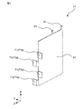
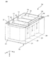
- FIG. 1 is a perspective view showing a capacitor module 1 according to the first embodiment of the present invention.
- FIG. 2 is a perspective view of the capacitor module 1 of FIG. 1 in which the case 91 is omitted.
- 3A and 3B are perspective views showing the capacitor 11 of the capacitor module of FIG.
- FIG. 4 is a side view of the capacitor module 1 of FIG.
- FIG. 5 is a perspective view showing the metal plate 51 of the capacitor module 1 of FIG.
- FIG. 6 is a perspective view showing the first bus bar 54 of the capacitor module 1 of FIG.
- FIG. 7 is a perspective view of the capacitor module 1 of FIG. 1 as viewed from another direction.
- the X, Y, and Z directions in the figure indicate the height direction, the horizontal direction, and the vertical direction of the capacitor module 1, respectively.
- the capacitor module 1 includes four capacitors 11 to 14, three metal plates 51 to 53, a first bus bar 54, and a second bus bar 55.
- the capacitor module 1 four capacitors 11 to 14, a metal plate 51 to 53, a part of the first bus bar 54, and a part of the second bus bar 55 are housed in a case 91 made of resin.
- the inside of the case 91 is filled with a sealing resin (not shown).
- the case 91 has an opening 92 formed at a position facing the bottom surface 93.
- the case 91 is formed of an insulating material, for example, a synthetic resin such as polyphenylene sulfide (PPS resin) or polybutylene terephthalate (PBT resin).
- PPS resin polyphenylene sulfide
- PBT resin polybutylene terephthalate
- the sealing resin is filled inside the case 91 to seal each component of the capacitor module 1.
- the sealing resin is a thermosetting resin, and for example, an epoxy resin can be used. Alternatively, it may be urethane resin.
- Capacitors 11 to 14 are film capacitors formed by winding a dielectric film.
- the capacitors 11 to 14 are formed by winding a dielectric film having a metal vapor deposition film formed on the surface thereof and pressing the wound body of the dielectric film into a flat shape.
- the capacitor module 1 includes four capacitors 11 to 14. Since the capacitors 11 to 14 have the same configuration, the capacitor 11 will be described here.
- the capacitor 11 has a first electrode 21, a second electrode 31, and a side surface 41.
- the first electrode 21 and the second electrode 31 are (end face) electrodes arranged so as to face each other.
- the side surface 41 is a side surface connecting the first electrode 21 and the second electrode 31.
- the side surface 41 has a pair of flat portions 41a facing each other and a pair of curved portions 41b connecting the pair of flat portions 41a to each other.
- the dielectric film of the capacitor 11 for example, a plastic film such as polyethylene terephthalate, polypropylene, polyphenylene sulfide, or polyethylene naphthalate can be used. Further, Al, Zn or the like can be used as the metal vapor deposition film formed on the surface of the plastic film.
- the first electrode 21 and the second electrode 31 are formed by spraying, for example, Zn or the like on the end portion of the wound dielectric film.
- the capacitors 11 to 14 are arranged in a row inside the case 91 so that the flat portions 41a to 44a face each other. That is, the flat portion 41a and the flat portion 42a face each other, the flat portion 42a and the flat portion 43a face each other, and the flat portion 43a and the flat portion 44a face each other. Capacitors 11 to 14 are arranged so that the distance between the flat portions 41a to 44a is about 0.5 mm to 4.0 mm. Further, the capacitors 11 to 14 are arranged so that the curved portions 41b to 44b on one side of the curved portions 41b to 44b face the opening 92 and the curved portions 41b to 44b on the other side face the bottom surface 93.
- the metal plates 51 to 53 are conductive members that electrically connect the first electrodes 21 to 24 of the capacitors 11 to 14 and the first bus bar 54, respectively.
- each of the metal plates 51 to 53 has a main body portion 61 to 63, an electrode contact portion 71 to 73, and a bus bar contact portion 81 to 83, respectively.
- the metal plates 51 to 53 have main bodies 61 to 63 arranged in a space between the flat portions 41a to 44a of the capacitors 11 to 14. That is, the metal plates 51 to 53 are formed between the flat portions 41a and 42a of the adjacent capacitors 11 and 12, between the flat portions 42a and 43a of the adjacent capacitors, and the flat portions of the adjacent capacitors 13 and 14, respectively. It is arranged between the portions 43a and 44a.
- the main body portion 61 of the metal plate 51 is arranged in the space S1 between the flat portion 41a and the flat portion 42a.
- the main body portion 62 of the metal plate 52 is arranged in the space S2 between the flat portion 42a and the flat portion 43a.
- the main body portion 63 of the metal plate 53 is arranged in the space S3 between the flat portion 43a and the flat portion 44a. That is, in the capacitor module 1, three metal plates 51 to 53 are arranged with respect to the four capacitors 11 to 14.
- the main body 61 of the metal plate 51 is a portion arranged in the space S1 between the flat portion 41a and the flat portion 42a.
- the space S1 is also filled with the sealing resin.
- the sealing resin enters between the main body portion 61 and the flat portion 41a and between the main body portion 61 and the flat portion 42a, the thermal conductivity is improved.
- the metal plate 51 is provided with an electrode contact portion 71 extending from the main body portion 61 so as to come into contact with the first electrodes 21 and 22.
- the electrode contact portion 71 is configured by bending a part of the end portion of the main body portion 61 in the vertical direction (Z direction) in the horizontal direction (Y direction).
- four electrode contact portions 71 are provided.
- the electrode contact portion 71a is bent so as to come into contact with the first electrode 21 of the capacitor 11 from the main body portion 61.
- the electrode contact portion 71b is bent so as to come into contact with the first electrode 22 of the capacitor 12 from the main body portion 61. That is, the electrode contact portion 71a and the electrode contact portion 71b are bent in different directions so that the metal plate 51 comes into contact with the first electrodes 21 and 22 of both the capacitors 11 and 12.
- they are alternately provided at intervals in the height direction (X direction).
- the electrode contact portions 71a and the electrode contact portions 71b By alternately providing the electrode contact portions 71a and the electrode contact portions 71b, the electrode contact portions 71 can be arranged in a well-balanced manner. Further, the electrode contact portion 71a and the electrode contact portion 71b can be evenly contacted with the first electrode 21 and the first electrode 22.
- the arrangement of the electrode contact portion 71a and the electrode contact portion 71b is not limited to this, and any configuration may be used as long as it can be connected to both the first electrode 21 of the capacitor 11 and the first electrode 22 of the capacitor 12.
- the electrode contact portion 71 is electrically connected to the first electrodes 21 and 22 by soldering. It is not necessary to solder all the electrode contact portions 71. For example, one of each of the two electrode contact portions 71a and one of the electrode contact portions 71b may be soldered, and the rest may be simply contacted with the first electrodes 21 and 22 without soldering. By appropriately selecting the electrode contact portion 71 to be soldered, it is possible to reduce the influence of heat on the characteristics of the capacitor module 1 at the time of soldering. By soldering all the electrode contact portions 71 and the first electrodes 21 and 22, the connection reliability between the metal plate 51 and the first electrodes 21 and 22 can be improved.
- the metal plate 51 is provided with a bus bar contact portion 81 extending from the main body portion 61 so as to come into contact with the first bus bar 54.
- the bus bar contact portion 81 is a portion to be inserted into a hole 64a (see FIG. 6) provided in the buried portion 64 of the first bus bar 54, which will be described later.
- the bus bar contact portion 81 is configured as a protruding portion in which a part of the end portion of the main body portion 61 in the X direction is further projected in the X direction.
- the bus bar contact portion 81 is located at a position where the main body portion 61 extends from the space S1 between the flat portions 41a and 42a toward the space S4 between the curved portions 41b and 42b. It is formed. That is, the bus bar contact portion 81 extends from between the flat portions 41a and 42a of the adjacent capacitors 11 and 12 to between the curved portions 41b and 52b of the capacitors 11 and 12, respectively. Is formed in. Similarly, the bus bar contact portion 82 is formed at a position where the main body portion 62 extends from the space S2 toward the space S5, and the bus bar contact portion 83 is formed at a position where the main body portion 63 extends from the space S3 toward the space S6. It is formed. The bus bar contact portions 81 to 83 are electrically connected to the first bus bar 54 by soldering.
- the metal plates 51 to 53 can be formed by, for example, pressing a metal plate having a thickness of about 0.3 mm to 0.5 mm.
- the metal plates 51 to 53 are made of a metal thinner than the first bus bar 54 described later. Since it is formed of a thin metal having a lower cost than the first bus bar 54, the manufacturing cost can be reduced by connecting the first electrodes 21 to 24 of the capacitors 11 to 14 to the first bus bar 54 via the metal plates 51 to 53. Can be reduced.
- the four capacitors 11 to 14 are arranged in a row, three spaces S1 to S3 are formed between the flat portions.
- one metal plate 51 to 53 is arranged in each of the three spaces S1 to S3.
- the heat dissipation of the capacitor module 1 can be improved.
- the first electrodes 21 to 24 of the capacitors 11 to 14 and the first bus bar 54 are used by using the metal plates 51 to 53 which are smaller than the number of the capacitors 11 to 14.
- Can be connected, and the configuration of the capacitor module 1 can be simplified.
- the metal plates 51 to 53 in the spaces S1 to S3, respectively the current flowing through the metal plates 51 to 53 can efficiently cancel the magnetic field due to the current flowing through the capacitors 11 to 14, and the capacitor module 1 is low. ESL can be planned.
- the spaces S1 to S3 between the flat portions are filled with a sealing resin.
- the heat generated from the capacitors 11 to 14 is conducted to the metal plates 51 to 53 through the sealing resin. Since the metal plates 51 to 53 are electrically and mechanically connected to the first bus bar 54, the heat of the capacitors 11 to 14 is efficiently transferred from the exposed portion 74 of the first bus bar 54 exposed to the outside of the sealing resin. The heat can be dissipated to the outside of the capacitor module 1.
- the metal plate 51 is in contact with any of the first electrodes 21 and 22 of the capacitors 11 and 12, respectively.
- the metal plate 52 contacts any of the first electrodes 22 and 23 of the capacitors 12 and 13, respectively, and the metal plate 53 touches any of the first electrodes 23 and 24 of the capacitors 13 and 14, respectively.
- the first electrode 21 of the capacitor 11 is in contact with the metal plate 51
- the first electrode 22 of the capacitor 12 is in contact with the metal plate 51 and the metal plate 52
- the first electrode 23 of the capacitor 13 is in contact with the metal plate 52.
- the first electrode 24 of the capacitor 14 comes into contact with the metal plate 53. That is, among the capacitors 11 to 14, the capacitors 12 and 13 arranged inside are in contact with two metal plates, respectively, and the capacitors 11 and 14 arranged outside are in contact with one metal plate, respectively.
- the present embodiment as shown in FIGS. 2 and 4, three metal plates 51 to 53 are arranged for the four capacitors 11 to 14.
- the capacitors 11 to 14 are arranged in a row so that the flat portions 41a to 44a face each other, the number of spaces S1 to S3 between the flat portions becomes three.
- the number of metal plates 51 to 53 are arranged in all the spaces S1 to S3, when the number of capacitors is 4, the number of metal plates is 3. That is, the number of metal plates is at most one less than the number of capacitors.
- the first bus bar 54 is a plate-shaped conductive member that is electrically connected to the first electrodes 21 to 24 of the capacitors 11 to 14.
- the first bus bar 54 is formed of a conductive member having a thickness of about 0.3 mm to 2 mm. As shown in FIG. 2, the first bus bar 54 and the respective first electrodes 21 to 24 are electrically connected to each other via the metal plates 51 to 53.
- the first bus bar 54 has three buried portions 64 and an exposed portion 74.
- the buried portion 64 is a portion connected to the bus bar contact portions 81 to 83 of the metal plates 51 to 53, and is embedded inside the sealing resin in the case 91.
- the exposed portion 74 is a portion exposed to the outside of the case 91.
- holes 64a are formed in each of the buried portions 64.
- the bus bar contact portions 81 to 83 of the metal plates 51 to 53 are inserted into the holes 64a and soldered to electrically connect the first bus bar 54 and the metal plates 51 to 53.
- the connection between the first bus bar 54 and the metal plates 51 to 53 is not limited to soldering, and can be performed by, for example, welding or a mechanical method such as caulking.
- the buried portion 64 of the first bus bar 54 is arranged at a position higher than the capacitors 11 to 14 in the height direction (X direction). Specifically, the buried portion 64 is arranged at a position closer to the opening 92 than the position H1 at the top of the curved portions 41b to 44b arranged toward the opening 92 of the capacitors 11 to 14. By arranging the buried portion 64 at this position, the metal plates 51 to 53 and the first bus bar 54 can be connected at a position away from the second electrodes 31 to 34. Therefore, it is possible to prevent a short circuit between the first bus bar 54 and the second electrodes 31 to 34.
- the second bus bar 55 is a plate-shaped conductive member electrically connected to the second electrodes 31 to 34 of the capacitors 11 to 14.
- the second bus bar 55 is formed of a conductive member having a thickness of about 0.3 mm to 2 mm.
- the second bus bar 55 has an exposed portion 65 exposed to the outside of the case 91, and an electrode contact portion 75 in contact with the second electrodes 31 to 34.
- the second bus bar 55 and the second electrodes 31 to 34 are electrically connected by soldering.
- the exposed portion 74 of the first bus bar 54 and the exposed portion 65 of the second bus bar 55 are arranged with a gap V1 of about 0.5 mm.
- V1 the distance between the exposed portion 74 of the first bus bar 54 and the exposed portion 65 of the second bus bar 55 to some extent, it is possible to reduce the ESL of the capacitor module 1. Therefore, it is preferable to arrange the exposed portion 74 and the exposed portion 65 so that the size of the interval V1 is about 0.5 mm.
- the capacitor module 1 includes four capacitors 11 to 14, three metal plates 51 to 53, a first bus bar 54, and a second bus bar 55.
- the capacitors 11 to 13 have first electrodes 21 to 24, second electrodes 31 to 34, and side surfaces 41 to 44, respectively.
- the first electrodes 21 to 24 and the second electrodes 31 to 34 are arranged so as to face each other.
- the side surfaces 41 to 44 connect the first electrodes 21 to 24 and the second electrodes 31 to 34, and have a pair of flat portions 41a to 44a facing each other, one flat portion 41a to 44a, and the other flat portions 41a to 44a. It has a pair of curved portions 41b to 44b that connect the above.
- the capacitors 11 to 14 are arranged in a row so that the flat portions 41a to 44a face each other.
- the metal plates 51 to 53 are arranged between the flat portions 41a to 44a of the adjacent capacitors 11 to 14, and are in contact with at least one of the first electrodes 21 to 24 of the adjacent capacitors 11 to 14, respectively.
- the first bus bar 54 is electrically connected to the metal plates 51 to 53.
- the second bus bar 55 is electrically connected to each of the second electrodes 31 to 34.
- the first electrodes 21 to 24 of the capacitors 11 to 14 are electrically connected to the metal plates 51 to 53, respectively.
- the metal plates 51 to 53 arranged between the flat portions 41a to 44a can cover any of the first electrodes 21 to 24 of the capacitors 11 to 14. Therefore, the metal plates 51 to 53 can improve the heat dissipation of the capacitor module 1 and simplify the configuration of the capacitor module 1.
- the metal plates 51 to 53 in the spaces S1 to S3, the magnetic field of the current flowing inside the capacitors 11 to 14 can be efficiently canceled, and the low ESL of the capacitor module 1 can be achieved.
- the metal plates 51 to 53 are bent in different directions so as to come into contact with the first electrodes 21 to 24 of both of the two adjacent capacitors 11 to 14.
- each of the metal plates 51 to 53 comes into contact with the first electrodes 21 to 24 of the two capacitors 11 to 14. Therefore, it is easy to change the design such as arranging a metal plate in all of the spaces S1 to S3 between the flat portions 41a to 44a, arranging the metal plate by thinning out, and the like. Further, by unifying the specifications of the metal plates 51 to 53, mass production of the metal plates 51 to 53 becomes possible, and the manufacturing cost can be suppressed.
- the metal plates 51 to 53 have a main body portion 61 to 63, an electrode contact portion 71 to 73, and a bus bar contact portion 81 to 83.
- the main body portions 61 to 63 are arranged between the flat portions 41a to 44a of the adjacent capacitors 11 to 14.
- the electrode contact portions 71 to 73 extend from the main body portions 61 to 63 so as to be in contact with the first electrodes 21 to 24.
- the bus bar contact portions 81 to 83 extend from the main body portions 61 to 63 so as to be in contact with the first bus bar 54, and are between the flat portions 41a to 44a (spaces S1 to S3) and between the curved portions 41b to 44b (space S4).
- the main body portions 61 to 63 are formed at positions extending toward S6).
- the metal plates 51 to 53 and the first bus bar 54 can be connected at a position away from the second electrodes 31 to 34. Therefore, it is possible to prevent a short circuit between the first bus bar 54 and the second electrodes 31 to 34.
- the number of capacitors 11 to 14 is m (m is a natural number of 3 or more), and the number of metal plates 51 to 53 is m-1. In the present embodiment, the number of capacitors 11 to 14 is 4, and the number of metal plates 51 to 53 is 3.
- the metal plates 51 to 53 can be arranged in any of the spaces S1 to S3 between the flat portions 41a to 44a. Therefore, it is possible to improve the heat dissipation of the capacitor module 1 while simplifying the configuration.
- the present invention is not limited to this.
- the three buried portions 64 of the first bus bar 54 do not necessarily have to be arranged at the same position in the height direction (X direction). Even when the positions in the height direction are different, the same effect as that of the first embodiment can be obtained.
- FIG. 8 is a perspective view of the capacitor module 1a according to the first modification of the first embodiment. As shown in FIG. 8, the capacitors 11 to 14 may be arranged so that the first electrodes 21 to 24 are arranged toward the bottom surface 93 and the second electrodes 31 to 34 are arranged toward the opening 92. ..
- FIG. 9 is a side view of the capacitor module 1b according to the second modification of the first embodiment.
- the buried portion 64b of the first bus bar 54b may be arranged at a position lower than the position H1 at the top of the curved portions 41b to 44b of the capacitors 11 to 14. That is, the buried portion 64b of the first bus bar 54b is arranged in each of the spaces S4 to S6 between the curved portions 41b to 44b.
- the dead space can be effectively utilized by locating the buried portion 64b at this position. Therefore, it contributes to the miniaturization of the capacitor module 1b.
- FIG. 10 is a perspective view of the capacitor module 1c according to the third modification of the first embodiment.
- the first bus bar 54c is provided with a cooling portion 76 extending from the exposed portion 74c, and the cooling portion 76 is provided with a thermal pad 77.
- the first bus bar 54c can be cooled in a larger area, so that the heat dissipation of the capacitor module 1c can be further improved.
- a thermal pad may be arranged on the first bus bar 54 of the capacitor module 1 of the first embodiment.
- the first bus bar 54 can be cooled by arranging the thermal pad on the exposed portion 74 of the first bus bar 54. Thereby, the heat dissipation effect of the capacitor module 1 can be further improved.
- FIG. 11 is an enlarged view of a part of the first bus bar 54d according to the modified example 4 of the first embodiment. As shown in FIG. 11, a recess 66 may be provided in a part of the buried portion 64d of the first bus bar 54d. By providing the recess 66 in the vicinity of the hole 64a into which the bus bar contact portion 83 of the metal plate 53 is inserted, it is possible to suppress heat escape during soldering.
- the second embodiment mainly describes the differences from the first embodiment.
- the same or equivalent configurations as those in the first embodiment will be described with the same reference numerals. Further, in the second embodiment, the description overlapping with the first embodiment is omitted.
- FIG. 12 is a side view of the capacitor module 2 according to the second embodiment.
- the number of metal plates 151 to 152 is different from that of the first embodiment. Specifically, of the spaces S1 to S3 between the flat portions, the metal plate 151 is arranged in the space S1, and the metal plate 152 is arranged in the space S3.
- the metal plates 151 and 152 can be connected to the first electrodes of two adjacent capacitors, respectively. Therefore, the metal plates 151 to 152 may be arranged so that any of the metal plates 151 to 152 is connected to all the first electrodes 21 to 24 without arranging them in all the spaces S1 to S3. ..
- the electrode contact portion 171a of the metal plate 151 is connected to the first electrode 21 of the capacitor 11, and the electrode contact portion 171b is connected to the first electrode 22 of the capacitor 12.
- the electrode contact portion 172a of the metal plate 152 is connected to the first electrode 23 of the capacitor 13, and the electrode contact portion 172b is connected to the first electrode 24 of the capacitor 14.
- the number of capacitors is an odd number, that is, when the number of capacitors is 2n + 1 (n is a natural number), the minimum number of metal plates is n + 1, and the maximum number of metal plates is 2n.
- n 2
- the number of a plurality of capacitors is 2n + 1 (n is a natural number), and the number of metal plates is n + 1 or more and 2n or less.
- the number of a plurality of capacitors is 2n (n is a natural number of 2 or more), and the number of metal plates is n or more and 2n-1 or less.
- the configuration of the capacitor module 2 can be simplified.
- FIG. 13 is a perspective view of the capacitor module 2a according to the modified example of the second embodiment. In FIG. 13, the case 91 and the capacitor 14 are omitted.
- the lengths of the metal plates 51a and 52a in the vertical direction (Z direction) are formed shorter than those of the metal plates 51 to 53 of the first embodiment.
- the vertical length of the metal plates 51a and 62a may be shortened to about 1 ⁇ 2 of the vertical length of the capacitors 11 to 14.
- the metal plates 51a and 52a can be arranged in the central portion of the capacitors 11 to 13, which are the portions that generate the most heat due to the ripple current flowing through the capacitors 11 to 13.
- the heat dissipation effect can be improved.
- the shapes of the first bus bar 154a and the second bus bar 155a may be different. Specifically, as shown in FIG. 13, the exposed portion 174a of the first bus bar 154a and the exposed portion 165a of the second bus bar 155a are formed so as to extend in the height direction (X direction). Even if the first bus bar 154a and the second bus bar 155a are arranged in this way, the same effect as that of the first embodiment can be obtained.
- the present invention is useful for capacitors used in various electronic devices, electrical devices, industrial devices, vehicle devices, and the like.
Landscapes
- Engineering & Computer Science (AREA)
- Power Engineering (AREA)
- Microelectronics & Electronic Packaging (AREA)
- Manufacturing & Machinery (AREA)
- Fixed Capacitors And Capacitor Manufacturing Machines (AREA)
- Inverter Devices (AREA)
Abstract
Provided is a capacitor module having a simplified configuration with improved heat dissipation. The capacitor module is provided with: a plurality of capacitors each having a first electrode and a second electrode opposing each other and a side surface connecting the first electrode and the second electrode, the side surface having a pair of flat portions opposing each other and a pair of curved portions connecting one flat portion with the other flat portion, the plurality of capacitors being disposed in a row with the flat portions opposing each other; at least one metal plate each disposed in any of gaps between the flat portions of adjacent capacitors and being in contact with the first electrode of at least one of the adjacent capacitors; a first bus-bar electrically connected to the at least one metal plate; and a second bus-bar electrically connected to each of the second electrodes. The first electrodes of the plurality of capacitors are electrically connected to the at least one metal plate.
Description
本発明は、コンデンサモジュールに関する。
The present invention relates to a capacitor module.
特許文献1には、複数の単位コンデンサを有するコンデンサにおいて、単位コンデンサそれぞれの一方の電極が、それぞれ異なる素子電極板に接続される構成が開示されている。
Patent Document 1 discloses a configuration in which one electrode of each unit capacitor is connected to a different element electrode plate in a capacitor having a plurality of unit capacitors.
特許文献1に記載のコンデンサは、放熱性と構成の簡素化の両立という点において未だ改善の余地がある。
The capacitor described in Patent Document 1 still has room for improvement in terms of achieving both heat dissipation and simplification of the configuration.
そこで、本発明は、放熱性を向上させつつ構成を簡素化したコンデンサモジュールを提供することを目的とする。
Therefore, an object of the present invention is to provide a capacitor module having a simplified configuration while improving heat dissipation.
本発明の一態様にかかるコンデンサモジュールは、
互いに対向する第1電極および第2電極と、第1電極と第2電極とを繋ぎ、互いに対向する一対の扁平部と一方の扁平部と他方の扁平部とを繋ぐ一対の湾曲部を有する側面とをそれぞれ有し、扁平部が対向するよう一列に配置された複数のコンデンサと、
隣接するコンデンサのそれぞれの扁平部の間のいずれかに配置され、隣接するコンデンサの少なくとも一方の第1電極にそれぞれ接触する少なくとも1つの金属板と、
少なくとも1つの金属板に電気的に接続する第1バスバーと、
第2電極のそれぞれに電気的に接続する第2バスバーと、
を備え、
複数のコンデンサの第1電極はそれぞれ、少なくとも1つの金属板に電気的に接続される。 The capacitor module according to one aspect of the present invention is
A side surface having a pair of flat portions facing each other, a pair of flat portions facing each other, and a pair of curved portions connecting one flat portion and the other flat portion, connecting the first electrode and the second electrode facing each other, and the first electrode and the second electrode. A plurality of capacitors arranged in a row so that the flat portions face each other, and
With at least one metal plate located between the respective flat portions of the adjacent capacitors and in contact with at least one of the first electrodes of the adjacent capacitors, respectively.
A first busbar that electrically connects to at least one metal plate,
A second bus bar that is electrically connected to each of the second electrodes,
Equipped with
Each of the first electrodes of the plurality of capacitors is electrically connected to at least one metal plate.
本発明によると、放熱性を向上させつつ構成を簡素化したコンデンサモジュールを提供することができる。
According to the present invention, it is possible to provide a capacitor module having a simplified configuration while improving heat dissipation.
(本発明に至った経緯)
特許文献1に記載のコンデンサは、単位コンデンサのそれぞれがコンデンサ素子と素子電極板とを有し、それぞれの素子電極板はそれぞれのコンデンサ素子の一方の電極に接続されている。それぞれの素子電極板は、各コンデンサに隣接して配置され、コンデンサ素子から発生する熱を素子電極板により放熱することができる。 (Background to the present invention)
In the capacitor described inPatent Document 1, each unit capacitor has a capacitor element and an element electrode plate, and each element electrode plate is connected to one electrode of each capacitor element. Each element electrode plate is arranged adjacent to each capacitor, and heat generated from the capacitor element can be dissipated by the element electrode plate.
特許文献1に記載のコンデンサは、単位コンデンサのそれぞれがコンデンサ素子と素子電極板とを有し、それぞれの素子電極板はそれぞれのコンデンサ素子の一方の電極に接続されている。それぞれの素子電極板は、各コンデンサに隣接して配置され、コンデンサ素子から発生する熱を素子電極板により放熱することができる。 (Background to the present invention)
In the capacitor described in
一方、1つのコンデンサ素子に1つの素子電極板が接続される構成であるため、コンデンサ素子の配置によっては、素子電極板の数が過剰となることがある。素子電極板の数が過剰となると、構成が煩雑となり、組み立て工程が複雑になるという課題がある。
On the other hand, since one element electrode plate is connected to one capacitor element, the number of element electrode plates may be excessive depending on the arrangement of the capacitor elements. If the number of element electrode plates is excessive, there is a problem that the configuration becomes complicated and the assembly process becomes complicated.
そこで、本発明者らは、放熱性を向上させつつ構成を簡素化したコンデンサモジュールを検討し、以下の発明に至った。
Therefore, the present inventors have studied a capacitor module having a simplified configuration while improving heat dissipation, and have reached the following invention.
本発明の一態様にかかるコンデンサモジュールは、
互いに対向する第1電極および第2電極と、第1電極と第2電極とを繋ぎ、互いに対向する一対の扁平部と一方の扁平部と他方の扁平部とを繋ぐ一対の湾曲部を有する側面とをそれぞれ有し、扁平部が対向するよう一列に配置された複数のコンデンサと、
隣接するコンデンサのそれぞれの扁平部の間のいずれかに配置され、隣接するコンデンサの少なくとも一方の第1電極にそれぞれ接触する少なくとも1つの金属板と、
少なくとも1つの金属板に電気的に接続する第1バスバーと、
第2電極のそれぞれに電気的に接続する第2バスバーと、
を備え、
複数のコンデンサの第1電極はそれぞれ、少なくとも1つの金属板に電気的に接続される。 The capacitor module according to one aspect of the present invention is
A side surface having a pair of flat portions facing each other, a pair of flat portions facing each other, and a pair of curved portions connecting one flat portion and the other flat portion, connecting the first electrode and the second electrode facing each other, and the first electrode and the second electrode. A plurality of capacitors arranged in a row so that the flat portions face each other, and
With at least one metal plate located between the respective flat portions of the adjacent capacitors and in contact with at least one of the first electrodes of the adjacent capacitors, respectively.
A first busbar that electrically connects to at least one metal plate,
A second bus bar that is electrically connected to each of the second electrodes,
Equipped with
Each of the first electrodes of the plurality of capacitors is electrically connected to at least one metal plate.
互いに対向する第1電極および第2電極と、第1電極と第2電極とを繋ぎ、互いに対向する一対の扁平部と一方の扁平部と他方の扁平部とを繋ぐ一対の湾曲部を有する側面とをそれぞれ有し、扁平部が対向するよう一列に配置された複数のコンデンサと、
隣接するコンデンサのそれぞれの扁平部の間のいずれかに配置され、隣接するコンデンサの少なくとも一方の第1電極にそれぞれ接触する少なくとも1つの金属板と、
少なくとも1つの金属板に電気的に接続する第1バスバーと、
第2電極のそれぞれに電気的に接続する第2バスバーと、
を備え、
複数のコンデンサの第1電極はそれぞれ、少なくとも1つの金属板に電気的に接続される。 The capacitor module according to one aspect of the present invention is
A side surface having a pair of flat portions facing each other, a pair of flat portions facing each other, and a pair of curved portions connecting one flat portion and the other flat portion, connecting the first electrode and the second electrode facing each other, and the first electrode and the second electrode. A plurality of capacitors arranged in a row so that the flat portions face each other, and
With at least one metal plate located between the respective flat portions of the adjacent capacitors and in contact with at least one of the first electrodes of the adjacent capacitors, respectively.
A first busbar that electrically connects to at least one metal plate,
A second bus bar that is electrically connected to each of the second electrodes,
Equipped with
Each of the first electrodes of the plurality of capacitors is electrically connected to at least one metal plate.
この構成によると、扁平部の間に配置した金属板が、複数のコンデンサのいずれの第1電極もカバーすることができる。このため、金属板により放熱性を向上させつつ、構成の簡素化を図ることができる。
According to this configuration, the metal plate arranged between the flat portions can cover any first electrode of the plurality of capacitors. Therefore, it is possible to simplify the configuration while improving the heat dissipation by the metal plate.
金属板は、隣接するコンデンサの両方の第1電極に接触するよう異なる方向に屈曲してもよい。
The metal plate may be bent in different directions so as to contact the first electrodes of both adjacent capacitors.
この構成によると、金属板のそれぞれが2つの第1電極に接触する。このため、扁平部の間のすべてに金属板を配置したり、間引いて配置したり、等の設計変更が容易になる。また、それぞれの金属板の仕様を統一することができるため、金属板を量産することができ製造コストを低減することができる。
According to this configuration, each of the metal plates comes into contact with the two first electrodes. Therefore, it is easy to change the design such as arranging the metal plate in all the spaces between the flat portions or decimating the metal plates. Further, since the specifications of each metal plate can be unified, the metal plates can be mass-produced and the manufacturing cost can be reduced.
金属板は、隣接するコンデンサのそれぞれの扁平部の間に配置される本体部と、本体部から第1電極に接触するように延びる電極接触部と、本体部から第1バスバーに接触するように延びるバスバー接触部と、を有し、
電極接触部は、隣接するコンデンサの一方のコンデンサの第1電極に接触する1つまたは複数の第1電極接触部と他方のコンデンサの第1電極に接触する1つまたは複数の第2電極接触部とが間隔を空けて交互に設けられて形成されてもよい。 The metal plate has a main body portion arranged between the flat portions of adjacent capacitors, an electrode contact portion extending from the main body portion so as to contact the first electrode, and a main body portion so as to contact the first bus bar. With an extended bus bar contact,
The electrode contact portion is one or more first electrode contact portions in contact with the first electrode of one of the adjacent capacitors and one or more second electrode contact portions in contact with the first electrode of the other capacitor. And may be formed alternately at intervals.
この構成によると、電極接触部をバランスよく配置することができる。
According to this configuration, the electrode contact parts can be arranged in a well-balanced manner.
バスバー接触部は、隣接するコンデンサのそれぞれの扁平部の間から隣接するコンデンサのそれぞれの湾曲部の間に向かって本体部が延びた位置に形成されてもよい。
The bus bar contact portion may be formed at a position where the main body portion extends from between the flat portions of the adjacent capacitors to the curved portions of the adjacent capacitors.
この構成によると、バスバー接触部を第2電極側に延ばした位置に設ける場合に比較して、バスバー接触部と第2電極との距離を離すことができる。このため、バスバー接触部と第2電極との短絡を防止することができる。
According to this configuration, the distance between the bus bar contact portion and the second electrode can be increased as compared with the case where the bus bar contact portion is provided at a position extended toward the second electrode side. Therefore, it is possible to prevent a short circuit between the bus bar contact portion and the second electrode.
バスバー接触部は、湾曲部の間に位置するよう形成されてもよい。
The bus bar contact portion may be formed so as to be located between the curved portions.
この構成によると、バスバー接触部を湾曲部の間のデッドスペースに配置することができる。このため、コンデンサモジュールの小型化に寄与する。
According to this configuration, the bus bar contact portion can be arranged in the dead space between the curved portions. Therefore, it contributes to the miniaturization of the capacitor module.
複数のコンデンサの数は2n+1(nは自然数)であり、金属板の数はn+1以上2n以下であってもよい。
The number of the plurality of capacitors is 2n + 1 (n is a natural number), and the number of metal plates may be n + 1 or more and 2n or less.
この構成によると、金属板の数をコンデンサの数よりも小さくしながら、隣接するコンデンサの間に配置した金属板に第1電極のそれぞれを接続することができる。このため、構成を簡素化して製造コストを抑制することができる。
According to this configuration, each of the first electrodes can be connected to a metal plate arranged between adjacent capacitors while making the number of metal plates smaller than the number of capacitors. Therefore, the configuration can be simplified and the manufacturing cost can be suppressed.
複数のコンデンサの数は2n(nは2以上の自然数)であり、金属板の数はn以上2n-1以下であってもよい。
The number of the plurality of capacitors is 2n (n is a natural number of 2 or more), and the number of metal plates may be n or more and 2n-1 or less.
この構成によると、金属板の数をコンデンサの数よりも小さくしながら、隣接するコンデンサの間に配置した金属板に第1電極のそれぞれを接続することができる。このため、構成を簡素化して製造コストを抑制することができる。
According to this configuration, each of the first electrodes can be connected to a metal plate arranged between adjacent capacitors while making the number of metal plates smaller than the number of capacitors. Therefore, the configuration can be simplified and the manufacturing cost can be suppressed.
複数のコンデンサの数はm(mは3以上の自然数)であり、金属板の数はm-1であってもよい。
The number of a plurality of capacitors is m (m is a natural number of 3 or more), and the number of metal plates may be m-1.
この構成によると、扁平部の間のいずれにも金属板を配置することができる。このため、コンデンサモジュールの放熱性を向上することができる。
According to this configuration, a metal plate can be placed anywhere between the flat portions. Therefore, the heat dissipation of the capacitor module can be improved.
以下、本発明にかかる実施の形態1について、添付の図面を参照しながら説明する。また、各図においては、説明を容易なものとするため、各要素を誇張して示している。
Hereinafter, the first embodiment according to the present invention will be described with reference to the attached drawings. Further, in each figure, each element is exaggerated for the sake of easy explanation.
(実施の形態1)
[全体構成]
図1は、本発明の実施の形態1にかかるコンデンサモジュール1を示す斜視図である。図2は、図1のコンデンサモジュール1のケース91を省略した斜視図である。図3Aおよび図3Bは、図1のコンデンサモジュールのコンデンサ11を示す斜視図である。図4は、図1のコンデンサモジュール1の側面図である。図5は、図1のコンデンサモジュール1の金属板51を示す斜視図である。図6は、図1のコンデンサモジュール1の第1バスバー54を示す斜視図である。図7は、図1のコンデンサモジュール1を別の方向から見た斜視図である。なお、図中のX、Y、Z方向はそれぞれ、コンデンサモジュール1の高さ方向、横方向、縦方向を示す。 (Embodiment 1)
[overall structure]
FIG. 1 is a perspective view showing acapacitor module 1 according to the first embodiment of the present invention. FIG. 2 is a perspective view of the capacitor module 1 of FIG. 1 in which the case 91 is omitted. 3A and 3B are perspective views showing the capacitor 11 of the capacitor module of FIG. FIG. 4 is a side view of the capacitor module 1 of FIG. FIG. 5 is a perspective view showing the metal plate 51 of the capacitor module 1 of FIG. FIG. 6 is a perspective view showing the first bus bar 54 of the capacitor module 1 of FIG. FIG. 7 is a perspective view of the capacitor module 1 of FIG. 1 as viewed from another direction. The X, Y, and Z directions in the figure indicate the height direction, the horizontal direction, and the vertical direction of the capacitor module 1, respectively.
[全体構成]
図1は、本発明の実施の形態1にかかるコンデンサモジュール1を示す斜視図である。図2は、図1のコンデンサモジュール1のケース91を省略した斜視図である。図3Aおよび図3Bは、図1のコンデンサモジュールのコンデンサ11を示す斜視図である。図4は、図1のコンデンサモジュール1の側面図である。図5は、図1のコンデンサモジュール1の金属板51を示す斜視図である。図6は、図1のコンデンサモジュール1の第1バスバー54を示す斜視図である。図7は、図1のコンデンサモジュール1を別の方向から見た斜視図である。なお、図中のX、Y、Z方向はそれぞれ、コンデンサモジュール1の高さ方向、横方向、縦方向を示す。 (Embodiment 1)
[overall structure]
FIG. 1 is a perspective view showing a
コンデンサモジュール1は、図1および図2に示すように、4つのコンデンサ11~14と、3つの金属板51~53と、第1バスバー54と、第2バスバー55と、を備える。コンデンサモジュール1は、樹脂により形成されたケース91に、4つのコンデンサ11~14と、金属板51~53と、第1バスバー54の一部と、第2バスバー55の一部とが収容され、ケース91の内部に封止樹脂(図示省略)が充填されている。
As shown in FIGS. 1 and 2, the capacitor module 1 includes four capacitors 11 to 14, three metal plates 51 to 53, a first bus bar 54, and a second bus bar 55. In the capacitor module 1, four capacitors 11 to 14, a metal plate 51 to 53, a part of the first bus bar 54, and a part of the second bus bar 55 are housed in a case 91 made of resin. The inside of the case 91 is filled with a sealing resin (not shown).
ケース91は、底面93に対向する位置に開口部92が形成されている。ケース91は、絶縁性材料で形成され、例えば、ポリフェニレンサルファイド(PPS樹脂)、ポリブチレンテレフタレート(PBT樹脂)等の合成樹脂により形成される。
The case 91 has an opening 92 formed at a position facing the bottom surface 93. The case 91 is formed of an insulating material, for example, a synthetic resin such as polyphenylene sulfide (PPS resin) or polybutylene terephthalate (PBT resin).
封止樹脂は、ケース91の内部に充填されてコンデンサモジュール1のそれぞれの構成要素を封止する。封止樹脂は、熱硬化性の樹脂であり、例えばエポキシ樹脂を使用することができる。または、ウレタン樹脂であってもよい。
The sealing resin is filled inside the case 91 to seal each component of the capacitor module 1. The sealing resin is a thermosetting resin, and for example, an epoxy resin can be used. Alternatively, it may be urethane resin.
<コンデンサ>
コンデンサ11~14は、誘電体フィルムを巻回して形成されたフィルムコンデンサである。コンデンサ11~14は、表面に金属蒸着膜を形成した誘電体フィルムを巻回し、誘電体フィルムの巻回体を扁平形状にプレスすることにより形成される。本実施の形態では、コンデンサモジュール1には、4つのコンデンサ11~14が含まれている。コンデンサ11~14は同様の構成であるため、ここではコンデンサ11について説明する。 <Capacitor>
Capacitors 11 to 14 are film capacitors formed by winding a dielectric film. The capacitors 11 to 14 are formed by winding a dielectric film having a metal vapor deposition film formed on the surface thereof and pressing the wound body of the dielectric film into a flat shape. In the present embodiment, the capacitor module 1 includes four capacitors 11 to 14. Since the capacitors 11 to 14 have the same configuration, the capacitor 11 will be described here.
コンデンサ11~14は、誘電体フィルムを巻回して形成されたフィルムコンデンサである。コンデンサ11~14は、表面に金属蒸着膜を形成した誘電体フィルムを巻回し、誘電体フィルムの巻回体を扁平形状にプレスすることにより形成される。本実施の形態では、コンデンサモジュール1には、4つのコンデンサ11~14が含まれている。コンデンサ11~14は同様の構成であるため、ここではコンデンサ11について説明する。 <Capacitor>
コンデンサ11は、図3Aおよび図3Bに示すように、第1電極21と、第2電極31と、側面41とを有する。第1電極21と第2電極31とは、互いに対向するよう配置された(端面)電極である。側面41は、第1電極21と第2電極31とを繋ぐ側面である。側面41は、互いに対向する一対の扁平部41aと、一対の扁平部41aどうしを繋ぐ一対の湾曲部41bとを有する。
As shown in FIGS. 3A and 3B, the capacitor 11 has a first electrode 21, a second electrode 31, and a side surface 41. The first electrode 21 and the second electrode 31 are (end face) electrodes arranged so as to face each other. The side surface 41 is a side surface connecting the first electrode 21 and the second electrode 31. The side surface 41 has a pair of flat portions 41a facing each other and a pair of curved portions 41b connecting the pair of flat portions 41a to each other.
コンデンサ11の誘電体フィルムとして、例えば、ポリエチレンテレフタレート、ポリプロピレン、ポリフェニレンサルファイド、またはポリエチレンナフタレート等のプラスチックフィルムを使用することができる。また、プラスチックフィルムの表面に形成される金属蒸着膜としては、Al、Zn等を使用することができる。巻回した誘電体フィルムの端部に、例えば、Zn等を溶射することにより第1電極21および第2電極31が形成される。
As the dielectric film of the capacitor 11, for example, a plastic film such as polyethylene terephthalate, polypropylene, polyphenylene sulfide, or polyethylene naphthalate can be used. Further, Al, Zn or the like can be used as the metal vapor deposition film formed on the surface of the plastic film. The first electrode 21 and the second electrode 31 are formed by spraying, for example, Zn or the like on the end portion of the wound dielectric film.
コンデンサ11~14は、図2および図4に示すように、ケース91の内部で、扁平部41a~44aどうしが対向するよう一列に配置される。すなわち、扁平部41aおよび扁平部42aが対向し、扁平部42aおよび扁平部43aが対向し、扁平部43aおよび扁平部44aが対向する。扁平部41a~44aどうしの隙間の距離は、0.5mm~4.0mm程度となるようにコンデンサ11~14が配列される。また、コンデンサ11~14は、湾曲部41b~44bのうち、一方側の湾曲部41b~44bが開口部92を向き、他方側の湾曲部41b~44bが底面93に向くよう配置されている。
As shown in FIGS. 2 and 4, the capacitors 11 to 14 are arranged in a row inside the case 91 so that the flat portions 41a to 44a face each other. That is, the flat portion 41a and the flat portion 42a face each other, the flat portion 42a and the flat portion 43a face each other, and the flat portion 43a and the flat portion 44a face each other. Capacitors 11 to 14 are arranged so that the distance between the flat portions 41a to 44a is about 0.5 mm to 4.0 mm. Further, the capacitors 11 to 14 are arranged so that the curved portions 41b to 44b on one side of the curved portions 41b to 44b face the opening 92 and the curved portions 41b to 44b on the other side face the bottom surface 93.
<金属板>
金属板51~53は、図2に示すように、コンデンサ11~14のそれぞれの第1電極21~24と第1バスバー54とを電気的に接続する導電性部材である。金属板51~53はそれぞれ、図2および図4に示すように、本体部61~63と、電極接触部71~73と、バスバー接触部81~83と、を有する。 <Metal plate>
As shown in FIG. 2, themetal plates 51 to 53 are conductive members that electrically connect the first electrodes 21 to 24 of the capacitors 11 to 14 and the first bus bar 54, respectively. As shown in FIGS. 2 and 4, each of the metal plates 51 to 53 has a main body portion 61 to 63, an electrode contact portion 71 to 73, and a bus bar contact portion 81 to 83, respectively.
金属板51~53は、図2に示すように、コンデンサ11~14のそれぞれの第1電極21~24と第1バスバー54とを電気的に接続する導電性部材である。金属板51~53はそれぞれ、図2および図4に示すように、本体部61~63と、電極接触部71~73と、バスバー接触部81~83と、を有する。 <Metal plate>
As shown in FIG. 2, the
金属板51~53は、図2および図4に示すように、本体部61~63がコンデンサ11~14の扁平部41a~44aどうしの間のスペースに配置される。すなわち、金属板51~53は隣接するコンデンサ11、12のそれぞれの扁平部41a、42aの間、隣接するコンデンサのそれぞれの扁平部42a、43aの間、および隣接するコンデンサ13、14のそれぞれの扁平部43a、44aの間に配置される。本実施の形態では、扁平部41aと扁平部42aの間のスペースS1に金属板51の本体部61が配置される。同様に、扁平部42aと扁平部43aとの間のスペースS2に金属板52の本体部62が配置される。さらに、扁平部43aと扁平部44aの間のスペースS3に金属板53の本体部63が配置される。すなわち、コンデンサモジュール1には、4つのコンデンサ11~14に対して、3つの金属板51~53が配置されている。
As shown in FIGS. 2 and 4, the metal plates 51 to 53 have main bodies 61 to 63 arranged in a space between the flat portions 41a to 44a of the capacitors 11 to 14. That is, the metal plates 51 to 53 are formed between the flat portions 41a and 42a of the adjacent capacitors 11 and 12, between the flat portions 42a and 43a of the adjacent capacitors, and the flat portions of the adjacent capacitors 13 and 14, respectively. It is arranged between the portions 43a and 44a. In the present embodiment, the main body portion 61 of the metal plate 51 is arranged in the space S1 between the flat portion 41a and the flat portion 42a. Similarly, the main body portion 62 of the metal plate 52 is arranged in the space S2 between the flat portion 42a and the flat portion 43a. Further, the main body portion 63 of the metal plate 53 is arranged in the space S3 between the flat portion 43a and the flat portion 44a. That is, in the capacitor module 1, three metal plates 51 to 53 are arranged with respect to the four capacitors 11 to 14.
金属板51~53は同様の構成であるため、図5を参照して、金属板51の構成を説明する。
Since the metal plates 51 to 53 have the same configuration, the configuration of the metal plate 51 will be described with reference to FIG.
金属板51の本体部61は、扁平部41aと扁平部42aとの間のスペースS1に配置される部分である。金属板51の本体部61をスペースS1に配置すると、ケース91の内部に封止樹脂を充填したときに、スペースS1にも封止樹脂が充填される。このとき、本体部61と扁平部41aとの間および本体部61と扁平部42aとの間に封止樹脂が入り込むため、熱伝導性が向上する。
The main body 61 of the metal plate 51 is a portion arranged in the space S1 between the flat portion 41a and the flat portion 42a. When the main body 61 of the metal plate 51 is arranged in the space S1, when the sealing resin is filled inside the case 91, the space S1 is also filled with the sealing resin. At this time, since the sealing resin enters between the main body portion 61 and the flat portion 41a and between the main body portion 61 and the flat portion 42a, the thermal conductivity is improved.
金属板51には、本体部61から第1電極21、22に接触するよう延びる電極接触部71が設けられている。電極接触部71は、本体部61の縦方向(Z方向)の端部の一部を横方向(Y方向)に折り曲げて構成される。本実施の形態では、図5に示すように、4つの電極接触部71(2つの電極接触部71aおよび2つの電極接触部71b)が設けられている。電極接触部71aは、本体部61からコンデンサ11の第1電極21に接触するよう屈曲している。電極接触部71bは、本体部61からコンデンサ12の第1電極22に接触するように屈曲されている。すなわち、金属板51が2つのコンデンサ11、12の両方の第1電極21、22に接触するよう、電極接触部71aと電極接触部71bとが異なる方向に屈曲している。
The metal plate 51 is provided with an electrode contact portion 71 extending from the main body portion 61 so as to come into contact with the first electrodes 21 and 22. The electrode contact portion 71 is configured by bending a part of the end portion of the main body portion 61 in the vertical direction (Z direction) in the horizontal direction (Y direction). In the present embodiment, as shown in FIG. 5, four electrode contact portions 71 (two electrode contact portions 71a and two electrode contact portions 71b) are provided. The electrode contact portion 71a is bent so as to come into contact with the first electrode 21 of the capacitor 11 from the main body portion 61. The electrode contact portion 71b is bent so as to come into contact with the first electrode 22 of the capacitor 12 from the main body portion 61. That is, the electrode contact portion 71a and the electrode contact portion 71b are bent in different directions so that the metal plate 51 comes into contact with the first electrodes 21 and 22 of both the capacitors 11 and 12.
本実施の形態では、コンデンサ11の第1電極21に接触する電極接触部(第1電極接触部)71aとコンデンサ12の第1電極22に接触する電極接触部(第2電極接触部)71bとが、高さ方向(X方向)に間隔を空けて交互に設けられている。電極接触部71aと電極接触部71bとが交互に設けられることにより、電極接触部71をバランス良く配置することができる。また、電極接触部71aと電極接触部71bとを、第1電極21と第1電極22に対して均等に接触させることができる。電極接触部71aと電極接触部71bとの配置はこれに限定されず、コンデンサ11の第1電極21とコンデンサ12の第1電極22との両方に接続できるような構成であればよい。
In the present embodiment, the electrode contact portion (first electrode contact portion) 71a in contact with the first electrode 21 of the capacitor 11 and the electrode contact portion (second electrode contact portion) 71b in contact with the first electrode 22 of the capacitor 12 However, they are alternately provided at intervals in the height direction (X direction). By alternately providing the electrode contact portions 71a and the electrode contact portions 71b, the electrode contact portions 71 can be arranged in a well-balanced manner. Further, the electrode contact portion 71a and the electrode contact portion 71b can be evenly contacted with the first electrode 21 and the first electrode 22. The arrangement of the electrode contact portion 71a and the electrode contact portion 71b is not limited to this, and any configuration may be used as long as it can be connected to both the first electrode 21 of the capacitor 11 and the first electrode 22 of the capacitor 12.
電極接触部71は、半田により第1電極21、22と電気的に接続される。なお、すべての電極接触部71を半田付けしなくてもよい。例えば、2つある電極接触部71aと電極接触部71bのそれぞれ1つずつを半田付けし、残りは半田付けせずに、第1電極21、22のそれぞれに接触させるだけでもよい。半田付けする電極接触部71を適宜選択することで、半田付けの際の熱によるコンデンサモジュール1の特性への影響を低減することができる。すべての電極接触部71と第1電極21、22とを半田付けすることで、金属板51と第1電極21、22との接続信頼性を向上することができる。
The electrode contact portion 71 is electrically connected to the first electrodes 21 and 22 by soldering. It is not necessary to solder all the electrode contact portions 71. For example, one of each of the two electrode contact portions 71a and one of the electrode contact portions 71b may be soldered, and the rest may be simply contacted with the first electrodes 21 and 22 without soldering. By appropriately selecting the electrode contact portion 71 to be soldered, it is possible to reduce the influence of heat on the characteristics of the capacitor module 1 at the time of soldering. By soldering all the electrode contact portions 71 and the first electrodes 21 and 22, the connection reliability between the metal plate 51 and the first electrodes 21 and 22 can be improved.
また、金属板51には、図2および図5に示すように、本体部61から第1バスバー54に接触するように延びるバスバー接触部81が設けられている。バスバー接触部81は、後述する第1バスバー54の埋没部64に設けられた穴64a(図6参照)に挿入される部分である。バスバー接触部81は、本体部61のX方向の端部の一部をX方向にさらに突出させた突出部として構成される。
Further, as shown in FIGS. 2 and 5, the metal plate 51 is provided with a bus bar contact portion 81 extending from the main body portion 61 so as to come into contact with the first bus bar 54. The bus bar contact portion 81 is a portion to be inserted into a hole 64a (see FIG. 6) provided in the buried portion 64 of the first bus bar 54, which will be described later. The bus bar contact portion 81 is configured as a protruding portion in which a part of the end portion of the main body portion 61 in the X direction is further projected in the X direction.
本実施の形態では、バスバー接触部81は、図4に示すように、扁平部41a、42aどうしのスペースS1から湾曲部41b、42bどうしのスペースS4に向かって、本体部61の延びた位置に形成されている。すなわち、バスバー接触部81は、隣接するコンデンサ11、12のそれぞれの扁平部41a、42aの間から、コンデンサ11、12のそれぞれの湾曲部41b、52bの間に向かって本体部61の延びた位置に形成される。同様に、バスバー接触部82は、スペースS2からスペースS5に向かって本体部62の延びた位置に形成され、バスバー接触部83は、スペースS3からスペースS6に向かって本体部63の延びた位置に形成される。バスバー接触部81~83は、半田により、第1バスバー54と電気的に接続される。
In the present embodiment, as shown in FIG. 4, the bus bar contact portion 81 is located at a position where the main body portion 61 extends from the space S1 between the flat portions 41a and 42a toward the space S4 between the curved portions 41b and 42b. It is formed. That is, the bus bar contact portion 81 extends from between the flat portions 41a and 42a of the adjacent capacitors 11 and 12 to between the curved portions 41b and 52b of the capacitors 11 and 12, respectively. Is formed in. Similarly, the bus bar contact portion 82 is formed at a position where the main body portion 62 extends from the space S2 toward the space S5, and the bus bar contact portion 83 is formed at a position where the main body portion 63 extends from the space S3 toward the space S6. It is formed. The bus bar contact portions 81 to 83 are electrically connected to the first bus bar 54 by soldering.
金属板51~53は、0.3mm~0.5mm程度の厚さの金属の板を、例えばプレス加工することにより形成することができる。金属板51~53は、後述する第1バスバー54よりも薄い金属により形成されている。第1バスバー54よりもコストの低い薄い金属により形成されるため、コンデンサ11~14の第1電極21~24を金属板51~53を介して第1バスバー54と接続することにより、製造コストを低減することができる。
The metal plates 51 to 53 can be formed by, for example, pressing a metal plate having a thickness of about 0.3 mm to 0.5 mm. The metal plates 51 to 53 are made of a metal thinner than the first bus bar 54 described later. Since it is formed of a thin metal having a lower cost than the first bus bar 54, the manufacturing cost can be reduced by connecting the first electrodes 21 to 24 of the capacitors 11 to 14 to the first bus bar 54 via the metal plates 51 to 53. Can be reduced.
コンデンサ11~14の4つのコンデンサが一列に配列されるため、扁平部どうしの間のスペースS1~S3は3つ形成される。本実施の形態では、図4に示すように、3つのスペースS1~S3にそれぞれ1つずつ金属板51~53が配置されている。3つのスペースS1~S3に1つずつ金属板51~53が配置されることにより、コンデンサモジュール1の放熱性を向上させることができる。また、このような金属板51~53の配置により、コンデンサ11~14の数よりも少ない金属板51~53を用いて、コンデンサ11~14の第1電極21~24それぞれと第1バスバー54とを接続することができ、コンデンサモジュール1の構成を簡素化することができる。また、スペースS1~S3にそれぞれ金属板51~53を配置することにより、金属板51~53を流れる電流がコンデンサ11~14を流れる電流による磁場を効率よく打ち消すことができ、コンデンサモジュール1の低ESLを図ることができる。
Since the four capacitors 11 to 14 are arranged in a row, three spaces S1 to S3 are formed between the flat portions. In the present embodiment, as shown in FIG. 4, one metal plate 51 to 53 is arranged in each of the three spaces S1 to S3. By arranging the metal plates 51 to 53 one by one in each of the three spaces S1 to S3, the heat dissipation of the capacitor module 1 can be improved. Further, due to such arrangement of the metal plates 51 to 53, the first electrodes 21 to 24 of the capacitors 11 to 14 and the first bus bar 54 are used by using the metal plates 51 to 53 which are smaller than the number of the capacitors 11 to 14. Can be connected, and the configuration of the capacitor module 1 can be simplified. Further, by arranging the metal plates 51 to 53 in the spaces S1 to S3, respectively, the current flowing through the metal plates 51 to 53 can efficiently cancel the magnetic field due to the current flowing through the capacitors 11 to 14, and the capacitor module 1 is low. ESL can be planned.
また、扁平部どうしの間のスペースS1~S3には、封止樹脂が充填される。コンデンサ11~14から発生した熱は、封止樹脂を通して金属板51~53に伝導する。金属板51~53は、第1バスバー54に電気的および機械的に接続しているため、封止樹脂の外部に露出する第1バスバー54の露出部74からコンデンサ11~14の熱を効率よくコンデンサモジュール1の外部に放熱することができる。
Further, the spaces S1 to S3 between the flat portions are filled with a sealing resin. The heat generated from the capacitors 11 to 14 is conducted to the metal plates 51 to 53 through the sealing resin. Since the metal plates 51 to 53 are electrically and mechanically connected to the first bus bar 54, the heat of the capacitors 11 to 14 is efficiently transferred from the exposed portion 74 of the first bus bar 54 exposed to the outside of the sealing resin. The heat can be dissipated to the outside of the capacitor module 1.
また、本実施の形態では、図2に示すように、金属板51は、コンデンサ11、12のそれぞれの第1電極21、22のいずれにも接触している。同様に、金属板52は、コンデンサ12、13のそれぞれの第1電極22、23のいずれにも接触し、金属板53は、コンデンサ13、14のそれぞれの第1電極23、24のいずれにも接触している。換言すると、コンデンサ11の第1電極21は金属板51に接触し、コンデンサ12の第1電極22は金属板51と金属板52とに接触し、コンデンサ13の第1電極23は金属板52と金属板53とに接触し、コンデンサ14の第1電極24は金属板53に接触する。つまり、コンデンサ11~14のうち、内側に配置されたコンデンサ12およびコンデンサ13はそれぞれ、2つの金属板と接触し、外側に配置されたコンデンサ11、14はそれぞれ、1つの金属板と接触する。
Further, in the present embodiment, as shown in FIG. 2, the metal plate 51 is in contact with any of the first electrodes 21 and 22 of the capacitors 11 and 12, respectively. Similarly, the metal plate 52 contacts any of the first electrodes 22 and 23 of the capacitors 12 and 13, respectively, and the metal plate 53 touches any of the first electrodes 23 and 24 of the capacitors 13 and 14, respectively. Are in contact. In other words, the first electrode 21 of the capacitor 11 is in contact with the metal plate 51, the first electrode 22 of the capacitor 12 is in contact with the metal plate 51 and the metal plate 52, and the first electrode 23 of the capacitor 13 is in contact with the metal plate 52. It comes into contact with the metal plate 53, and the first electrode 24 of the capacitor 14 comes into contact with the metal plate 53. That is, among the capacitors 11 to 14, the capacitors 12 and 13 arranged inside are in contact with two metal plates, respectively, and the capacitors 11 and 14 arranged outside are in contact with one metal plate, respectively.
本実施の形態では、図2および図4に示すように、4つのコンデンサ11~14に対して、3つの金属板51~53が配置されている。扁平部41a~44aどうしが対向するよう一列にコンデンサ11~14を配置すると、扁平部どうしの間のスペースS1~S3の数は3つとなる。本実施の形態では、すべてのスペースS1~S3に金属板51~53を配置するため、コンデンサの数が4である場合、金属板の数が3となる。すなわち、金属板の数は、最大でコンデンサの数より1少ない数となる。
In the present embodiment, as shown in FIGS. 2 and 4, three metal plates 51 to 53 are arranged for the four capacitors 11 to 14. When the capacitors 11 to 14 are arranged in a row so that the flat portions 41a to 44a face each other, the number of spaces S1 to S3 between the flat portions becomes three. In the present embodiment, since the metal plates 51 to 53 are arranged in all the spaces S1 to S3, when the number of capacitors is 4, the number of metal plates is 3. That is, the number of metal plates is at most one less than the number of capacitors.
<第1バスバー>
第1バスバー54は、コンデンサ11~14の第1電極21~24と電気的に接続される板状の導電性部材である。第1バスバー54は、0.3mm~2mm程度の厚さの導電性部材により形成される。第1バスバー54とそれぞれの第1電極21~24とは、図2に示すように、金属板51~53を介して電気的に接続されている。 <1st bus bar>
Thefirst bus bar 54 is a plate-shaped conductive member that is electrically connected to the first electrodes 21 to 24 of the capacitors 11 to 14. The first bus bar 54 is formed of a conductive member having a thickness of about 0.3 mm to 2 mm. As shown in FIG. 2, the first bus bar 54 and the respective first electrodes 21 to 24 are electrically connected to each other via the metal plates 51 to 53.
第1バスバー54は、コンデンサ11~14の第1電極21~24と電気的に接続される板状の導電性部材である。第1バスバー54は、0.3mm~2mm程度の厚さの導電性部材により形成される。第1バスバー54とそれぞれの第1電極21~24とは、図2に示すように、金属板51~53を介して電気的に接続されている。 <1st bus bar>
The
第1バスバー54は、図2および図6に示すように、3つの埋没部64と、露出部74と、を有する。埋没部64は、金属板51~53のバスバー接触部81~83と接続される部分であり、ケース91内で封止樹脂の内部に埋設される。露出部74は、ケース91の外側に露出する部分である。
As shown in FIGS. 2 and 6, the first bus bar 54 has three buried portions 64 and an exposed portion 74. The buried portion 64 is a portion connected to the bus bar contact portions 81 to 83 of the metal plates 51 to 53, and is embedded inside the sealing resin in the case 91. The exposed portion 74 is a portion exposed to the outside of the case 91.
図6に示すように、埋没部64のそれぞれには、穴64aが形成されている。穴64aには、金属板51~53のバスバー接触部81~83が挿入され、半田付けされることにより、第1バスバー54と金属板51~53とが電気的に接続される。なお、第1バスバー54と金属板51~53との接続は、半田付けに限定されず、例えば、溶接、またはカシメ等の機械的な方法等により行うことができる。
As shown in FIG. 6, holes 64a are formed in each of the buried portions 64. The bus bar contact portions 81 to 83 of the metal plates 51 to 53 are inserted into the holes 64a and soldered to electrically connect the first bus bar 54 and the metal plates 51 to 53. The connection between the first bus bar 54 and the metal plates 51 to 53 is not limited to soldering, and can be performed by, for example, welding or a mechanical method such as caulking.
本実施の形態では、図4に示すように、第1バスバー54の埋没部64は、高さ方向(X方向)において、コンデンサ11~14よりも高い位置に配置される。具体的には、コンデンサ11~14の開口部92に向かって配置される湾曲部41b~44bの頂部の位置H1よりも、開口部92に近い位置に埋没部64が配置されている。埋没部64をこの位置に配置することにより、金属板51~53と第1バスバー54の接続を、第2電極31~34から離れた位置で行うことができる。このため、第1バスバー54と第2電極31~34との短絡を防止することができる。
In the present embodiment, as shown in FIG. 4, the buried portion 64 of the first bus bar 54 is arranged at a position higher than the capacitors 11 to 14 in the height direction (X direction). Specifically, the buried portion 64 is arranged at a position closer to the opening 92 than the position H1 at the top of the curved portions 41b to 44b arranged toward the opening 92 of the capacitors 11 to 14. By arranging the buried portion 64 at this position, the metal plates 51 to 53 and the first bus bar 54 can be connected at a position away from the second electrodes 31 to 34. Therefore, it is possible to prevent a short circuit between the first bus bar 54 and the second electrodes 31 to 34.
<第2バスバー>
第2バスバー55は、図7に示すように、コンデンサ11~14の第2電極31~34と電気的に接続される板状の導電性部材である。第2バスバー55は、0.3mm~2mm程度の厚さの導電性部材により形成される。第2バスバー55は、ケース91の外部に露出する露出部65と、第2電極31~34に接触する電極接触部75と、を有する。第2バスバー55と第2電極31~34とは、半田付けにより電気的に接続される。 <2nd bus bar>
As shown in FIG. 7, thesecond bus bar 55 is a plate-shaped conductive member electrically connected to the second electrodes 31 to 34 of the capacitors 11 to 14. The second bus bar 55 is formed of a conductive member having a thickness of about 0.3 mm to 2 mm. The second bus bar 55 has an exposed portion 65 exposed to the outside of the case 91, and an electrode contact portion 75 in contact with the second electrodes 31 to 34. The second bus bar 55 and the second electrodes 31 to 34 are electrically connected by soldering.
第2バスバー55は、図7に示すように、コンデンサ11~14の第2電極31~34と電気的に接続される板状の導電性部材である。第2バスバー55は、0.3mm~2mm程度の厚さの導電性部材により形成される。第2バスバー55は、ケース91の外部に露出する露出部65と、第2電極31~34に接触する電極接触部75と、を有する。第2バスバー55と第2電極31~34とは、半田付けにより電気的に接続される。 <2nd bus bar>
As shown in FIG. 7, the
第1バスバー54の露出部74と第2バスバー55の露出部65とは、0.5mm程度の間隔V1を空けて配置されている。第1バスバー54の露出部74と第2バスバー55の露出部65との間隔V1をある程度小さくすることで、コンデンサモジュール1の低ESL化を実現することができる。このため、間隔V1の大きさが0.5mm程度になるよう、露出部74と露出部65とを配置するとよい。
The exposed portion 74 of the first bus bar 54 and the exposed portion 65 of the second bus bar 55 are arranged with a gap V1 of about 0.5 mm. By reducing the distance V1 between the exposed portion 74 of the first bus bar 54 and the exposed portion 65 of the second bus bar 55 to some extent, it is possible to reduce the ESL of the capacitor module 1. Therefore, it is preferable to arrange the exposed portion 74 and the exposed portion 65 so that the size of the interval V1 is about 0.5 mm.
[効果]
実施の形態1にかかるコンデンサモジュール1によれば、以下の効果を奏することができる。 [effect]
According to thecapacitor module 1 according to the first embodiment, the following effects can be obtained.
実施の形態1にかかるコンデンサモジュール1によれば、以下の効果を奏することができる。 [effect]
According to the
コンデンサモジュール1は、4つのコンデンサ11~14と、3つの金属板51~53と、第1バスバー54と、第2バスバー55とを備える。コンデンサ11~13は、第1電極21~24および第2電極31~34と、側面41~44と、をそれぞれ有する。第1電極21~24と第2電極31~34とは、互いに対向するよう配置される。側面41~44は、第1電極21~24と第2電極31~34とを繋ぎ、互いに対向する一対の扁平部41a~44aと、一方の扁平部41a~44aと他方の扁平部41a~44aとを繋ぐ一対の湾曲部41b~44bと、を有する。コンデンサ11~14は、扁平部41a~44aが対向するよう一列に配置される。金属板51~53は、隣接するコンデンサ11~14の扁平部41a~44aの間のいずれかに配置され、隣接するコンデンサ11~14の少なくとも一方の第1電極21~24にそれぞれ接触する。第1バスバー54は、金属板51~53に電気的に接続する。第2バスバー55は、第2電極31~34のそれぞれに電気的に接続する。コンデンサ11~14の第1電極21~24はそれぞれ、金属板51~53に電気的に接続される。
The capacitor module 1 includes four capacitors 11 to 14, three metal plates 51 to 53, a first bus bar 54, and a second bus bar 55. The capacitors 11 to 13 have first electrodes 21 to 24, second electrodes 31 to 34, and side surfaces 41 to 44, respectively. The first electrodes 21 to 24 and the second electrodes 31 to 34 are arranged so as to face each other. The side surfaces 41 to 44 connect the first electrodes 21 to 24 and the second electrodes 31 to 34, and have a pair of flat portions 41a to 44a facing each other, one flat portion 41a to 44a, and the other flat portions 41a to 44a. It has a pair of curved portions 41b to 44b that connect the above. The capacitors 11 to 14 are arranged in a row so that the flat portions 41a to 44a face each other. The metal plates 51 to 53 are arranged between the flat portions 41a to 44a of the adjacent capacitors 11 to 14, and are in contact with at least one of the first electrodes 21 to 24 of the adjacent capacitors 11 to 14, respectively. The first bus bar 54 is electrically connected to the metal plates 51 to 53. The second bus bar 55 is electrically connected to each of the second electrodes 31 to 34. The first electrodes 21 to 24 of the capacitors 11 to 14 are electrically connected to the metal plates 51 to 53, respectively.
このような構成により、扁平部41a~44aの間(スペースS1~S3)に配置した金属板51~53が、コンデンサ11~14のいずれの第1電極21~24もカバーすることができる。このため、金属板51~53によりコンデンサモジュール1の放熱性を向上させつつ、コンデンサモジュール1の構成の簡素化を図ることができる。
With such a configuration, the metal plates 51 to 53 arranged between the flat portions 41a to 44a (spaces S1 to S3) can cover any of the first electrodes 21 to 24 of the capacitors 11 to 14. Therefore, the metal plates 51 to 53 can improve the heat dissipation of the capacitor module 1 and simplify the configuration of the capacitor module 1.
また、スペースS1~S3に金属板51~53を配置することにより、コンデンサ11~14の内部を流れる電流の磁場を効率よく打ち消すことができ、コンデンサモジュール1の低ESLを図ることができる。
Further, by arranging the metal plates 51 to 53 in the spaces S1 to S3, the magnetic field of the current flowing inside the capacitors 11 to 14 can be efficiently canceled, and the low ESL of the capacitor module 1 can be achieved.
また、金属板51~53は、隣接する2つのコンデンサ11~14の両方の第1電極21~24に接触するよう異なる方向に屈曲する。
Further, the metal plates 51 to 53 are bent in different directions so as to come into contact with the first electrodes 21 to 24 of both of the two adjacent capacitors 11 to 14.
このような構成により、金属板51~53のそれぞれが2つのコンデンサ11~14の第1電極21~24に接触する。このため、扁平部41a~44aどうしの間のスペースS1~S3のすべてに金属板を配置したり、間引いて金属板を配置したり、等の設計変更が容易になる。また、金属板51~53の仕様を統一することで、金属板51~53の量産が可能となり、製造コストを抑制することができる。
With such a configuration, each of the metal plates 51 to 53 comes into contact with the first electrodes 21 to 24 of the two capacitors 11 to 14. Therefore, it is easy to change the design such as arranging a metal plate in all of the spaces S1 to S3 between the flat portions 41a to 44a, arranging the metal plate by thinning out, and the like. Further, by unifying the specifications of the metal plates 51 to 53, mass production of the metal plates 51 to 53 becomes possible, and the manufacturing cost can be suppressed.
また、金属板51~53は、本体部61~63と、電極接触部71~73と、バスバー接触部81~83と、を有する。本体部61~63は、隣接するコンデンサ11~14のそれぞれの扁平部41a~44aの間に配置される。電極接触部71~73は、本体部61~63から、第1電極21~24に接触するように延びる。バスバー接触部81~83は、本体部61~63から、第1バスバー54に接触するように延び、扁平部41a~44aの間(スペースS1~S3)から湾曲部41b~44bの間(スペースS4~S6)に向かって本体部61~63が延びた位置に形成される。
Further, the metal plates 51 to 53 have a main body portion 61 to 63, an electrode contact portion 71 to 73, and a bus bar contact portion 81 to 83. The main body portions 61 to 63 are arranged between the flat portions 41a to 44a of the adjacent capacitors 11 to 14. The electrode contact portions 71 to 73 extend from the main body portions 61 to 63 so as to be in contact with the first electrodes 21 to 24. The bus bar contact portions 81 to 83 extend from the main body portions 61 to 63 so as to be in contact with the first bus bar 54, and are between the flat portions 41a to 44a (spaces S1 to S3) and between the curved portions 41b to 44b (space S4). The main body portions 61 to 63 are formed at positions extending toward S6).
このような構成により、金属板51~53と第1バスバー54の接続を、第2電極31~34から離れた位置で行うことができる。このため、第1バスバー54と第2電極31~34との短絡を防止することができる。
With such a configuration, the metal plates 51 to 53 and the first bus bar 54 can be connected at a position away from the second electrodes 31 to 34. Therefore, it is possible to prevent a short circuit between the first bus bar 54 and the second electrodes 31 to 34.
また、コンデンサ11~14の数がm(mは3以上の自然数)であり、金属板51~53の数はm-1である。本実施の形態では、コンデンサ11~14の数が4であり、金属板51~53の数が3である。
Further, the number of capacitors 11 to 14 is m (m is a natural number of 3 or more), and the number of metal plates 51 to 53 is m-1. In the present embodiment, the number of capacitors 11 to 14 is 4, and the number of metal plates 51 to 53 is 3.
このような構成により、扁平部41a~44aどうしの間のいずれのスペースS1~S3にも金属板51~53を配置することができる。このため、構成の簡素化を図りつつ、コンデンサモジュール1の放熱性を向上させることができる。
With such a configuration, the metal plates 51 to 53 can be arranged in any of the spaces S1 to S3 between the flat portions 41a to 44a. Therefore, it is possible to improve the heat dissipation of the capacitor module 1 while simplifying the configuration.
[変形例]
なお、実施の形態1では、4つのコンデンサ11~14を備える例について説明したが、コンデンサの数は4つに限らず、3つ以上のコンデンサが備えられていればよい。 [Modification example]
In the first embodiment, an example including fourcapacitors 11 to 14 has been described, but the number of capacitors is not limited to four, and three or more capacitors may be provided.
なお、実施の形態1では、4つのコンデンサ11~14を備える例について説明したが、コンデンサの数は4つに限らず、3つ以上のコンデンサが備えられていればよい。 [Modification example]
In the first embodiment, an example including four
また、実施の形態1では、図4に示すように、第1バスバー54の埋没部64が、高さ方向(X方向)において同じ位置に配置される例について説明したが、これに限定されない。第1バスバー54の3つの埋没部64は、必ずしも高さ方向(X方向)において同じ位置に配置されなくてもよい。高さ方向の位置が異なる場合であっても、実施の形態1と同様の効果を奏することができる。
Further, in the first embodiment, as shown in FIG. 4, an example in which the buried portion 64 of the first bus bar 54 is arranged at the same position in the height direction (X direction) has been described, but the present invention is not limited to this. The three buried portions 64 of the first bus bar 54 do not necessarily have to be arranged at the same position in the height direction (X direction). Even when the positions in the height direction are different, the same effect as that of the first embodiment can be obtained.
また、実施の形態1では、コンデンサ11~14の一対の湾曲部41b~44bがそれぞれ、ケース91の開口部92および底面93に向かうよう配置される例に説明したが、コンデンサ11~14の配置はこれに限定されない。図8は、実施の形態1の変形例1にかかるコンデンサモジュール1aの斜視図である。図8に示すように、第1電極21~24が底面93に向かって配置され、第2電極31~34が開口部92に向かって配置されるよう、コンデンサ11~14が配置されてもよい。
Further, in the first embodiment, the example in which the pair of curved portions 41b to 44b of the capacitors 11 to 14 are arranged so as to face the opening 92 and the bottom surface 93 of the case 91, respectively, has been described, but the arrangement of the capacitors 11 to 14 has been described. Is not limited to this. FIG. 8 is a perspective view of the capacitor module 1a according to the first modification of the first embodiment. As shown in FIG. 8, the capacitors 11 to 14 may be arranged so that the first electrodes 21 to 24 are arranged toward the bottom surface 93 and the second electrodes 31 to 34 are arranged toward the opening 92. ..
このような構成により、実施の形態1と同様の効果を奏することができる。
With such a configuration, the same effect as that of the first embodiment can be obtained.
また、実施の形態1では、図4に示すように、第1バスバー54の埋没部64が、開口部92に向かって配置されたコンデンサ11~14の湾曲部41b~44bの頂部の位置H1よりも高い位置に配置される例について説明したが、これに限定されない。図9は、実施の形態1の変形例2にかかるコンデンサモジュール1bの側面図である。図9に示すように、第1バスバー54bの埋没部64bが、コンデンサ11~14の湾曲部41b~44bの頂部の位置H1よりも低い位置に配置されてもよい。すなわち、第1バスバー54bの埋没部64bが、湾曲部41b~44bどうしの間のスペースS4~S6のそれぞれに配置される。
Further, in the first embodiment, as shown in FIG. 4, the buried portion 64 of the first bus bar 54 is located at the top position H1 of the curved portions 41b to 44b of the capacitors 11 to 14 arranged toward the opening 92. Although the example of being placed at a high position has been described, the present invention is not limited to this. FIG. 9 is a side view of the capacitor module 1b according to the second modification of the first embodiment. As shown in FIG. 9, the buried portion 64b of the first bus bar 54b may be arranged at a position lower than the position H1 at the top of the curved portions 41b to 44b of the capacitors 11 to 14. That is, the buried portion 64b of the first bus bar 54b is arranged in each of the spaces S4 to S6 between the curved portions 41b to 44b.
湾曲部41b、42bどうしのスペースS4~S6は、ケース91内でデッドスペースとなるため、この位置に埋没部64bが位置することでデッドスペースを有効活用することができる。このため、コンデンサモジュール1bの小型化に寄与する。
Since the spaces S4 to S6 between the curved portions 41b and 42b become dead spaces in the case 91, the dead space can be effectively utilized by locating the buried portion 64b at this position. Therefore, it contributes to the miniaturization of the capacitor module 1b.
また、第1バスバー54に、サーマルパッドを配置するための冷却部を設けてもよい。図10は、実施の形態1の変形例3にかかるコンデンサモジュール1cの斜視図である。コンデンサモジュール1cでは、第1バスバー54cに露出部74cから延びた冷却部76が設けられ、冷却部76にサーマルパッド77が配置されている。このような構成により、より大きな面積で第1バスバー54cを冷却することができるため、コンデンサモジュール1cの放熱性をさらに向上することができる。
Further, the first bus bar 54 may be provided with a cooling unit for arranging the thermal pad. FIG. 10 is a perspective view of the capacitor module 1c according to the third modification of the first embodiment. In the condenser module 1c, the first bus bar 54c is provided with a cooling portion 76 extending from the exposed portion 74c, and the cooling portion 76 is provided with a thermal pad 77. With such a configuration, the first bus bar 54c can be cooled in a larger area, so that the heat dissipation of the capacitor module 1c can be further improved.
また、実施の形態1のコンデンサモジュール1の第1バスバー54に、サーマルパッドが配置されていてもよい。具体的には、第1バスバー54の露出部74にサーマルパッドを配置することで、第1バスバー54を冷却することができる。これにより、コンデンサモジュール1の放熱効果をさらに向上させることができる。
Further, a thermal pad may be arranged on the first bus bar 54 of the capacitor module 1 of the first embodiment. Specifically, the first bus bar 54 can be cooled by arranging the thermal pad on the exposed portion 74 of the first bus bar 54. Thereby, the heat dissipation effect of the capacitor module 1 can be further improved.
また、第1バスバーの埋没部の形状が異なっていてもよい。図11は、実施の形態1の変形例4にかかる第1バスバー54dの一部を拡大した図である。図11に示すように、第1バスバー54dの埋没部64dの一部に凹部66が設けられていてもよい。金属板53のバスバー接触部83を挿入する穴64aの近傍に凹部66が設けられることにより、半田付けの際の熱の逃げを抑制することができる。
Further, the shape of the buried portion of the first bus bar may be different. FIG. 11 is an enlarged view of a part of the first bus bar 54d according to the modified example 4 of the first embodiment. As shown in FIG. 11, a recess 66 may be provided in a part of the buried portion 64d of the first bus bar 54d. By providing the recess 66 in the vicinity of the hole 64a into which the bus bar contact portion 83 of the metal plate 53 is inserted, it is possible to suppress heat escape during soldering.
(実施の形態2)
本発明の実施の形態2にかかるコンデンサモジュール2について説明する。 (Embodiment 2)
Thecapacitor module 2 according to the second embodiment of the present invention will be described.
本発明の実施の形態2にかかるコンデンサモジュール2について説明する。 (Embodiment 2)
The
実施の形態2では、主に実施の形態1と異なる点について説明する。実施の形態2においては、実施の形態1と同一または同等の構成については同じ符号を付して説明する。また、実施の形態2では、実施の形態1と重複する記載は省略する。
The second embodiment mainly describes the differences from the first embodiment. In the second embodiment, the same or equivalent configurations as those in the first embodiment will be described with the same reference numerals. Further, in the second embodiment, the description overlapping with the first embodiment is omitted.
図12は、実施の形態2にかかるコンデンサモジュール2の側面図である。
FIG. 12 is a side view of the capacitor module 2 according to the second embodiment.
実施の形態2では、図12に示すように、金属板151~152の数が実施の形態1と異なる。具体的には、扁平部どうしの間のスペースS1~S3のうち、スペースS1に金属板151が配置され、スペースS3に金属板152が配置される。金属板151、152はそれぞれ、隣接する2つのコンデンサの第1電極に接続することができる。このため、すべてのスペースS1~S3に配置しなくても、すべての第1電極21~24にいずれかの金属板151~152が接続されるよう、金属板151~152が配置されればよい。本実施の形態では、金属板151の電極接触部171aがコンデンサ11の第1電極21に接続され、電極接触部171bがコンデンサ12の第1電極22に接続される。同様に、金属板152の電極接触部172aがコンデンサ13の第1電極23に接続され、電極接触部172bがコンデンサ14の第1電極24に接続される。2つの金属板151、152が配置される場合、第1バスバー154の埋没部164も2か所設けられる。
In the second embodiment, as shown in FIG. 12, the number of metal plates 151 to 152 is different from that of the first embodiment. Specifically, of the spaces S1 to S3 between the flat portions, the metal plate 151 is arranged in the space S1, and the metal plate 152 is arranged in the space S3. The metal plates 151 and 152 can be connected to the first electrodes of two adjacent capacitors, respectively. Therefore, the metal plates 151 to 152 may be arranged so that any of the metal plates 151 to 152 is connected to all the first electrodes 21 to 24 without arranging them in all the spaces S1 to S3. .. In the present embodiment, the electrode contact portion 171a of the metal plate 151 is connected to the first electrode 21 of the capacitor 11, and the electrode contact portion 171b is connected to the first electrode 22 of the capacitor 12. Similarly, the electrode contact portion 172a of the metal plate 152 is connected to the first electrode 23 of the capacitor 13, and the electrode contact portion 172b is connected to the first electrode 24 of the capacitor 14. When two metal plates 151 and 152 are arranged, two buried portions 164 of the first bus bar 154 are also provided.
本実施の形態では、コンデンサ11~14の数が4つであるため、扁平部どうしの間のスペースS1~S3は3つ形成される。したがって、金属板は、最大でコンデンサの数より1小さい数を配置することができる。また、コンデンサの数が偶数の場合、金属板は、最小でコンデンサの数の1/2の数を配置することができる。すなわち、コンデンサの数が2n(nは2以上の自然数)である場合、金属板の数はn以上2n-1以下である。本実施の形態では、n=2であり、コンデンサの数は2n=4、金属板の数はn=2である。
In the present embodiment, since the number of capacitors 11 to 14 is four, three spaces S1 to S3 are formed between the flat portions. Therefore, the number of metal plates can be arranged up to one smaller than the number of capacitors. Further, when the number of capacitors is an even number, the metal plate can be arranged with a minimum number of 1/2 of the number of capacitors. That is, when the number of capacitors is 2n (n is a natural number of 2 or more), the number of metal plates is n or more and 2n-1 or less. In this embodiment, n = 2, the number of capacitors is 2n = 4, and the number of metal plates is n = 2.
また、コンデンサの数が奇数の場合、すなわち、コンデンサの数が2n+1(nは自然数)である場合、金属板の最小数はn+1であり、金属板の最大数は2nである。例えば、n=2とすると、コンデンサの数は2n+1=5、金属板の最小数はn+1=3であり、金属板の最大数は2n=4である。
Further, when the number of capacitors is an odd number, that is, when the number of capacitors is 2n + 1 (n is a natural number), the minimum number of metal plates is n + 1, and the maximum number of metal plates is 2n. For example, assuming that n = 2, the number of capacitors is 2n + 1 = 5, the minimum number of metal plates is n + 1 = 3, and the maximum number of metal plates is 2n = 4.
[効果]
実施の形態2にかかるコンデンサモジュール2によれば、以下の効果を奏することができる。 [effect]
According to thecapacitor module 2 according to the second embodiment, the following effects can be obtained.
実施の形態2にかかるコンデンサモジュール2によれば、以下の効果を奏することができる。 [effect]
According to the
複数のコンデンサの数は2n+1(nは自然数)であり、金属板の数はn+1以上2n以下である。
The number of a plurality of capacitors is 2n + 1 (n is a natural number), and the number of metal plates is n + 1 or more and 2n or less.
複数のコンデンサの数は2n(nは2以上の自然数)であり、金属板の数はn以上2n-1以下である。
The number of a plurality of capacitors is 2n (n is a natural number of 2 or more), and the number of metal plates is n or more and 2n-1 or less.
金属板の数を減らすことにより、コンデンサモジュール2の構成を簡素化することができる。
By reducing the number of metal plates, the configuration of the capacitor module 2 can be simplified.
[変形例]
実施の形態2では、金属板51~53がコンデンサ11~14の扁平部41a~44aのほぼ全面にわたり配置される例について説明したが、これに限定されない。図13は、実施の形態2の変形例にかかるコンデンサモジュール2aの斜視図である。図13では、ケース91およびコンデンサ14が省略されている。 [Modification example]
In the second embodiment, an example in which themetal plates 51 to 53 are arranged over almost the entire flat portion 41a to 44a of the capacitors 11 to 14 has been described, but the present invention is not limited thereto. FIG. 13 is a perspective view of the capacitor module 2a according to the modified example of the second embodiment. In FIG. 13, the case 91 and the capacitor 14 are omitted.
実施の形態2では、金属板51~53がコンデンサ11~14の扁平部41a~44aのほぼ全面にわたり配置される例について説明したが、これに限定されない。図13は、実施の形態2の変形例にかかるコンデンサモジュール2aの斜視図である。図13では、ケース91およびコンデンサ14が省略されている。 [Modification example]
In the second embodiment, an example in which the
図13に示すように、金属板51a、52aの縦方向(Z方向)の長さが、実施の形態1の金属板51~53と比較して短く形成されている。金属板51a、62aの縦方向の長さは、コンデンサ11~14の縦方向の長さの1/2程度に短くしてもよい。このような構成により、コンデンサ11~13に流れるリップル電流により最も発熱する部分であるコンデンサ11~13の中央部に金属板51a、52aを配置することができる。コンデンサ11~13の中央部付近に金属板51a、52aを配置することにより、放熱効果を向上することができる。
As shown in FIG. 13, the lengths of the metal plates 51a and 52a in the vertical direction (Z direction) are formed shorter than those of the metal plates 51 to 53 of the first embodiment. The vertical length of the metal plates 51a and 62a may be shortened to about ½ of the vertical length of the capacitors 11 to 14. With such a configuration, the metal plates 51a and 52a can be arranged in the central portion of the capacitors 11 to 13, which are the portions that generate the most heat due to the ripple current flowing through the capacitors 11 to 13. By arranging the metal plates 51a and 52a near the center of the capacitors 11 to 13, the heat dissipation effect can be improved.
また、第1バスバー154aおよび第2バスバー155aの形状は異なっていてもよい。具体的には、図13に示すように、第1バスバー154aの露出部174aおよび第2バスバー155aの露出部165aが高さ方向(X方向)に延びて形成されている。第1バスバー154aおよび第2バスバー155aがこのように配置されていても、実施の形態1と同様の効果を奏することができる。
Further, the shapes of the first bus bar 154a and the second bus bar 155a may be different. Specifically, as shown in FIG. 13, the exposed portion 174a of the first bus bar 154a and the exposed portion 165a of the second bus bar 155a are formed so as to extend in the height direction (X direction). Even if the first bus bar 154a and the second bus bar 155a are arranged in this way, the same effect as that of the first embodiment can be obtained.
本発明は、添付図面を参照しながら好ましい実施の形態に関連して充分に記載されているが、この技術の熟練した人々にとっては種々の変形や修正は明白である。そのような変形や修正は、添付した特許請求の範囲による本発明の範囲から外れない限りにおいて、その中に含まれると理解されるべきである。
Although the present invention has been fully described in connection with preferred embodiments with reference to the accompanying drawings, various modifications and modifications are obvious to those skilled in the art. It should be understood that such modifications and modifications are included within the scope of the invention as long as it does not deviate from the scope of the invention according to the appended claims.
本発明は、各種電子機器、電気機器、産業機器、車両装置等に使用されるコンデンサに有用である。
The present invention is useful for capacitors used in various electronic devices, electrical devices, industrial devices, vehicle devices, and the like.
1、1a~1b、2、2a コンデンサモジュール
1a コンデンサモジュール
11~14 コンデンサ
21~24 第1電極
31~34 第2電極
41~44 側面
41a~44a 扁平部
41b~44b 湾曲部
51~53、 金属板
54 第1バスバー
55 第2バスバー
61~63 本体部
62 本体部
63 本体部
64 埋没部
71~73 電極接触部
81~83 バスバー接触部 1, 1a to 1b, 2,2a Capacitor module 1a Capacitor module 11 to 14 Capacitor 21 to 24 First electrode 31 to 34 Second electrode 41 to 44 Side surface 41a to 44a Flat portion 41b to 44b Curved portion 51 to 53, metal plate 54 1st bus bar 55 2nd bus bar 61-63 Main body 62 Main body 63 Main body 64 Buried part 71-73 Electrode contact part 81-83 Bus bar contact part
1a コンデンサモジュール
11~14 コンデンサ
21~24 第1電極
31~34 第2電極
41~44 側面
41a~44a 扁平部
41b~44b 湾曲部
51~53、 金属板
54 第1バスバー
55 第2バスバー
61~63 本体部
62 本体部
63 本体部
64 埋没部
71~73 電極接触部
81~83 バスバー接触部 1, 1a to 1b, 2,
Claims (8)
- 互いに対向する第1電極および第2電極と、前記第1電極と前記第2電極とを繋ぎ、互いに対向する一対の扁平部と一方の前記扁平部と他方の前記扁平部とを繋ぐ一対の湾曲部を有する側面とをそれぞれ有し、前記扁平部が対向するよう一列に配置された複数のコンデンサと、
隣接する前記コンデンサのそれぞれの前記扁平部の間のいずれかに配置され、前記隣接するコンデンサの少なくとも一方の前記第1電極に接触する少なくとも1つの金属板と、
前記少なくとも1つの金属板に電気的に接続する第1バスバーと、
前記第2電極のそれぞれに電気的に接続する第2バスバーと、
を備え、
前記複数のコンデンサの前記第1電極はそれぞれ、前記少なくとも1つの金属板に電気的に接続される、
コンデンサモジュール。 A pair of curved portions connecting the first electrode and the second electrode facing each other, the first electrode and the second electrode, and a pair of flat portions facing each other, one flat portion and the other flat portion. A plurality of capacitors having a side surface having a portion and arranged in a row so that the flat portions face each other, and a plurality of capacitors.
With at least one metal plate located between the flat portions of each of the adjacent capacitors and in contact with the first electrode of at least one of the adjacent capacitors.
A first bus bar electrically connected to the at least one metal plate,
A second bus bar electrically connected to each of the second electrodes,
Equipped with
Each of the first electrodes of the plurality of capacitors is electrically connected to the at least one metal plate.
Capacitor module. - 前記金属板は、前記隣接するコンデンサの両方の前記第1電極に接触するよう異なる方向に屈曲する、
請求項1に記載のコンデンサモジュール。 The metal plate bends in different directions to contact the first electrode of both adjacent capacitors.
The capacitor module according to claim 1. - 前記金属板は、前記隣接するコンデンサのそれぞれの前記扁平部の間に配置される本体部と、前記本体部から前記第1電極に接触するように延びる電極接触部と、前記本体部から前記第1バスバーに接触するように延びるバスバー接触部と、を有し、
前記電極接触部は、前記隣接するコンデンサの一方のコンデンサの前記第1電極に接触する1つまたは複数の第1電極接触部と他方のコンデンサの前記第1電極に接触する1つまたは複数の第2電極接触部とが間隔を空けて交互に設けられて形成される、
請求項1または2に記載のコンデンサモジュール。 The metal plate has a main body portion arranged between the flat portions of the adjacent capacitors, an electrode contact portion extending from the main body portion so as to contact the first electrode, and the main body portion to the first portion. 1 With a bus bar contact portion extending so as to come into contact with the bus bar,
The electrode contact portion is one or more first electrode contact portions in contact with the first electrode of one of the adjacent capacitors and one or more first electrodes in contact with the first electrode of the other capacitor. The two electrode contact portions are alternately provided at intervals.
The capacitor module according to claim 1 or 2. - 前記バスバー接触部は、前記隣接するコンデンサのそれぞれの前記扁平部の間から前記隣接するコンデンサのそれぞれの前記湾曲部の間に向かって前記本体部が延びた位置に形成される、
請求項3に記載のコンデンサモジュール。 The bus bar contact portion is formed at a position where the main body portion extends from between the flat portions of the adjacent capacitors to the curved portions of the adjacent capacitors.
The capacitor module according to claim 3. - 前記バスバー接触部は、前記湾曲部の間に位置するよう形成される、
請求項3または4に記載のコンデンサモジュール。 The bus bar contact portion is formed so as to be located between the curved portions.
The capacitor module according to claim 3 or 4. - 前記複数のコンデンサの数は2n+1(nは自然数)であり、前記金属板の数はn+1以上2n以下である、
請求項1ないし5のいずれか1項に記載のコンデンサモジュール。 The number of the plurality of capacitors is 2n + 1 (n is a natural number), and the number of the metal plates is n + 1 or more and 2n or less.
The capacitor module according to any one of claims 1 to 5. - 前記複数のコンデンサの数は2n(nは2以上の自然数)であり、前記金属板の数はn以上2n-1以下である、
請求項1ないし6のいずれか1項に記載のコンデンサモジュール。 The number of the plurality of capacitors is 2n (n is a natural number of 2 or more), and the number of the metal plates is n or more and 2n-1 or less.
The capacitor module according to any one of claims 1 to 6. - 前記複数のコンデンサの数はm(mは3以上の自然数)であり、前記金属板の数は、m-1である、
請求項1ないし7のいずれか1項に記載のコンデンサモジュール。 The number of the plurality of capacitors is m (m is a natural number of 3 or more), and the number of the metal plates is m-1.
The capacitor module according to any one of claims 1 to 7.
Priority Applications (3)
| Application Number | Priority Date | Filing Date | Title |
|---|---|---|---|
| JP2022526915A JP7452640B2 (en) | 2020-05-28 | 2021-05-18 | capacitor module |
| CN202190000473.5U CN219143983U (en) | 2020-05-28 | 2021-05-18 | Capacitor module |
| US17/994,042 US20230089940A1 (en) | 2020-05-28 | 2022-11-25 | Capacitor module |
Applications Claiming Priority (2)
| Application Number | Priority Date | Filing Date | Title |
|---|---|---|---|
| JP2020093502 | 2020-05-28 | ||
| JP2020-093502 | 2020-05-28 |
Related Child Applications (1)
| Application Number | Title | Priority Date | Filing Date |
|---|---|---|---|
| US17/994,042 Continuation US20230089940A1 (en) | 2020-05-28 | 2022-11-25 | Capacitor module |
Publications (1)
| Publication Number | Publication Date |
|---|---|
| WO2021241320A1 true WO2021241320A1 (en) | 2021-12-02 |
Family
ID=78744652
Family Applications (1)
| Application Number | Title | Priority Date | Filing Date |
|---|---|---|---|
| PCT/JP2021/018752 WO2021241320A1 (en) | 2020-05-28 | 2021-05-18 | Capacitor module |
Country Status (4)
| Country | Link |
|---|---|
| US (1) | US20230089940A1 (en) |
| JP (1) | JP7452640B2 (en) |
| CN (1) | CN219143983U (en) |
| WO (1) | WO2021241320A1 (en) |
Citations (4)
| Publication number | Priority date | Publication date | Assignee | Title |
|---|---|---|---|---|
| JPH01176919U (en) * | 1988-06-02 | 1989-12-18 | ||
| JPH09260180A (en) * | 1996-03-19 | 1997-10-03 | Shizuki Denki Seisakusho:Kk | Low inductance capacitor |
| WO2016002177A1 (en) * | 2014-07-02 | 2016-01-07 | パナソニックIpマネジメント株式会社 | Film capacitor |
| JP2020088064A (en) * | 2018-11-20 | 2020-06-04 | ルビコン電子株式会社 | Capacitor module |
-
2021
- 2021-05-18 CN CN202190000473.5U patent/CN219143983U/en active Active
- 2021-05-18 JP JP2022526915A patent/JP7452640B2/en active Active
- 2021-05-18 WO PCT/JP2021/018752 patent/WO2021241320A1/en active Application Filing
-
2022
- 2022-11-25 US US17/994,042 patent/US20230089940A1/en active Pending
Patent Citations (4)
| Publication number | Priority date | Publication date | Assignee | Title |
|---|---|---|---|---|
| JPH01176919U (en) * | 1988-06-02 | 1989-12-18 | ||
| JPH09260180A (en) * | 1996-03-19 | 1997-10-03 | Shizuki Denki Seisakusho:Kk | Low inductance capacitor |
| WO2016002177A1 (en) * | 2014-07-02 | 2016-01-07 | パナソニックIpマネジメント株式会社 | Film capacitor |
| JP2020088064A (en) * | 2018-11-20 | 2020-06-04 | ルビコン電子株式会社 | Capacitor module |
Also Published As
| Publication number | Publication date |
|---|---|
| JP7452640B2 (en) | 2024-03-19 |
| CN219143983U (en) | 2023-06-06 |
| US20230089940A1 (en) | 2023-03-23 |
| JPWO2021241320A1 (en) | 2021-12-02 |
Similar Documents
| Publication | Publication Date | Title |
|---|---|---|
| CN108352252B (en) | Thin film capacitor | |
| US8416556B2 (en) | Power capacitor | |
| JP4823116B2 (en) | Semiconductor module | |
| KR20060049377A (en) | Surface-mount capacitor and method of producing the same | |
| JP5897918B2 (en) | Capacitor | |
| JP2011155138A (en) | Capacitor | |
| JP6305731B2 (en) | Case mold type capacitor and manufacturing method thereof | |
| WO2018123584A1 (en) | Circuit structure and electrical connection box | |
| WO2021241320A1 (en) | Capacitor module | |
| JP2008270329A (en) | Capacitor | |
| JP7213408B2 (en) | capacitor | |
| CN112951605A (en) | Capacitor and electronic module assembly with low inductance connection features | |
| KR20190116143A (en) | Electronic component and board having the same mounted thereon | |
| JP7418374B2 (en) | bus bar module | |
| WO2022185803A1 (en) | Capacitor module | |
| JP7418375B2 (en) | bus bar module | |
| US20230386747A1 (en) | Electronic device | |
| JPWO2020003481A1 (en) | Electronic device | |
| JP7409491B2 (en) | capacitor module | |
| JP7484385B2 (en) | Circuit Board | |
| US20220262895A1 (en) | Semiconductor device and manufacturing method thereof | |
| JP4802616B2 (en) | LC composite parts | |
| JP2023008578A (en) | capacitor | |
| JP2024056186A (en) | Capacitor | |
| JP5982625B2 (en) | Capacitor and case mold type capacitor using this capacitor |
Legal Events
| Date | Code | Title | Description |
|---|---|---|---|
| 121 | Ep: the epo has been informed by wipo that ep was designated in this application |
Ref document number: 21813664 Country of ref document: EP Kind code of ref document: A1 |
|
| ENP | Entry into the national phase |
Ref document number: 2022526915 Country of ref document: JP Kind code of ref document: A |
|
| NENP | Non-entry into the national phase |
Ref country code: DE |
|
| 122 | Ep: pct application non-entry in european phase |
Ref document number: 21813664 Country of ref document: EP Kind code of ref document: A1 |