WO2021241127A1 - 電気光学基板、液晶表示装置および電子機器 - Google Patents
電気光学基板、液晶表示装置および電子機器 Download PDFInfo
- Publication number
- WO2021241127A1 WO2021241127A1 PCT/JP2021/017073 JP2021017073W WO2021241127A1 WO 2021241127 A1 WO2021241127 A1 WO 2021241127A1 JP 2021017073 W JP2021017073 W JP 2021017073W WO 2021241127 A1 WO2021241127 A1 WO 2021241127A1
- Authority
- WO
- WIPO (PCT)
- Prior art keywords
- liquid crystal
- electro
- display device
- transparent pixel
- crystal display
- Prior art date
- Legal status (The legal status is an assumption and is not a legal conclusion. Google has not performed a legal analysis and makes no representation as to the accuracy of the status listed.)
- Ceased
Links
Images










Classifications
-
- G—PHYSICS
- G02—OPTICS
- G02F—OPTICAL DEVICES OR ARRANGEMENTS FOR THE CONTROL OF LIGHT BY MODIFICATION OF THE OPTICAL PROPERTIES OF THE MEDIA OF THE ELEMENTS INVOLVED THEREIN; NON-LINEAR OPTICS; FREQUENCY-CHANGING OF LIGHT; OPTICAL LOGIC ELEMENTS; OPTICAL ANALOGUE/DIGITAL CONVERTERS
- G02F1/00—Devices or arrangements for the control of the intensity, colour, phase, polarisation or direction of light arriving from an independent light source, e.g. switching, gating or modulating; Non-linear optics
- G02F1/01—Devices or arrangements for the control of the intensity, colour, phase, polarisation or direction of light arriving from an independent light source, e.g. switching, gating or modulating; Non-linear optics for the control of the intensity, phase, polarisation or colour
- G02F1/13—Devices or arrangements for the control of the intensity, colour, phase, polarisation or direction of light arriving from an independent light source, e.g. switching, gating or modulating; Non-linear optics for the control of the intensity, phase, polarisation or colour based on liquid crystals, e.g. single liquid crystal display cells
- G02F1/133—Constructional arrangements; Operation of liquid crystal cells; Circuit arrangements
- G02F1/1333—Constructional arrangements; Manufacturing methods
- G02F1/1343—Electrodes
- G02F1/134309—Electrodes characterised by their geometrical arrangement
- G02F1/134336—Matrix
-
- G—PHYSICS
- G02—OPTICS
- G02F—OPTICAL DEVICES OR ARRANGEMENTS FOR THE CONTROL OF LIGHT BY MODIFICATION OF THE OPTICAL PROPERTIES OF THE MEDIA OF THE ELEMENTS INVOLVED THEREIN; NON-LINEAR OPTICS; FREQUENCY-CHANGING OF LIGHT; OPTICAL LOGIC ELEMENTS; OPTICAL ANALOGUE/DIGITAL CONVERTERS
- G02F1/00—Devices or arrangements for the control of the intensity, colour, phase, polarisation or direction of light arriving from an independent light source, e.g. switching, gating or modulating; Non-linear optics
- G02F1/01—Devices or arrangements for the control of the intensity, colour, phase, polarisation or direction of light arriving from an independent light source, e.g. switching, gating or modulating; Non-linear optics for the control of the intensity, phase, polarisation or colour
- G02F1/13—Devices or arrangements for the control of the intensity, colour, phase, polarisation or direction of light arriving from an independent light source, e.g. switching, gating or modulating; Non-linear optics for the control of the intensity, phase, polarisation or colour based on liquid crystals, e.g. single liquid crystal display cells
- G02F1/133—Constructional arrangements; Operation of liquid crystal cells; Circuit arrangements
- G02F1/1333—Constructional arrangements; Manufacturing methods
- G02F1/1335—Structural association of cells with optical devices, e.g. polarisers or reflectors
- G02F1/133509—Filters, e.g. light shielding masks
- G02F1/133512—Light shielding layers, e.g. black matrix
-
- G—PHYSICS
- G02—OPTICS
- G02F—OPTICAL DEVICES OR ARRANGEMENTS FOR THE CONTROL OF LIGHT BY MODIFICATION OF THE OPTICAL PROPERTIES OF THE MEDIA OF THE ELEMENTS INVOLVED THEREIN; NON-LINEAR OPTICS; FREQUENCY-CHANGING OF LIGHT; OPTICAL LOGIC ELEMENTS; OPTICAL ANALOGUE/DIGITAL CONVERTERS
- G02F1/00—Devices or arrangements for the control of the intensity, colour, phase, polarisation or direction of light arriving from an independent light source, e.g. switching, gating or modulating; Non-linear optics
- G02F1/01—Devices or arrangements for the control of the intensity, colour, phase, polarisation or direction of light arriving from an independent light source, e.g. switching, gating or modulating; Non-linear optics for the control of the intensity, phase, polarisation or colour
- G02F1/13—Devices or arrangements for the control of the intensity, colour, phase, polarisation or direction of light arriving from an independent light source, e.g. switching, gating or modulating; Non-linear optics for the control of the intensity, phase, polarisation or colour based on liquid crystals, e.g. single liquid crystal display cells
- G02F1/133—Constructional arrangements; Operation of liquid crystal cells; Circuit arrangements
- G02F1/1333—Constructional arrangements; Manufacturing methods
- G02F1/1335—Structural association of cells with optical devices, e.g. polarisers or reflectors
- G02F1/133528—Polarisers
- G02F1/133531—Polarisers characterised by the arrangement of polariser or analyser axes
-
- G—PHYSICS
- G02—OPTICS
- G02F—OPTICAL DEVICES OR ARRANGEMENTS FOR THE CONTROL OF LIGHT BY MODIFICATION OF THE OPTICAL PROPERTIES OF THE MEDIA OF THE ELEMENTS INVOLVED THEREIN; NON-LINEAR OPTICS; FREQUENCY-CHANGING OF LIGHT; OPTICAL LOGIC ELEMENTS; OPTICAL ANALOGUE/DIGITAL CONVERTERS
- G02F1/00—Devices or arrangements for the control of the intensity, colour, phase, polarisation or direction of light arriving from an independent light source, e.g. switching, gating or modulating; Non-linear optics
- G02F1/01—Devices or arrangements for the control of the intensity, colour, phase, polarisation or direction of light arriving from an independent light source, e.g. switching, gating or modulating; Non-linear optics for the control of the intensity, phase, polarisation or colour
- G02F1/13—Devices or arrangements for the control of the intensity, colour, phase, polarisation or direction of light arriving from an independent light source, e.g. switching, gating or modulating; Non-linear optics for the control of the intensity, phase, polarisation or colour based on liquid crystals, e.g. single liquid crystal display cells
- G02F1/133—Constructional arrangements; Operation of liquid crystal cells; Circuit arrangements
- G02F1/1333—Constructional arrangements; Manufacturing methods
- G02F1/1335—Structural association of cells with optical devices, e.g. polarisers or reflectors
- G02F1/133528—Polarisers
- G02F1/133548—Wire-grid polarisers
Definitions
- This disclosure relates to an electro-optical substrate, a liquid crystal display device, and an electronic device.
- An electro-optic substrate in which transparent pixel electrodes arranged in a matrix are arranged, a facing substrate arranged so as to face the electro-optical substrate, and a liquid crystal material layer enclosed between the electro-optic substrate and the facing substrate.
- a liquid crystal display device containing the above is known.
- the liquid crystal display device displays an image by operating the pixel as an optical shutter (light bulb).
- optical shutter light bulb
- liquid crystal display devices are required to have high definition as well as high brightness.
- the active matrix type liquid crystal display device After applying a voltage to the transparent pixel electrode via a switching element (for example, a transistor), the transistor is put into a non-conducting state. Then, the pixel capacitance holds the voltage to display the voltage. Therefore, when a leak current flows through a transistor that should be in a non-conducting state, the holding voltage changes, and as a result, the display quality deteriorates. Further, when light is incident on the transistor, carriers are induced and the leakage current increases.
- a switching element for example, a transistor
- Patent Document 1 discloses a technique of increasing the amount of emitted light and suppressing light incident on a transistor by providing a waveguide structure in an opening region.
- a phase shift called goose-henshen shift occurs in the light reflected at the interface. Therefore, a phase difference occurs between the light that passes through the waveguide without being reflected and the light that is reflected at the interface or the like and passes through. As a result, a part of the light emitted from the waveguide in the black display state passes through the polarizing element on the emitting side, or a part of the light emitted from the waveguide in the white display state is emitted. It may happen that it does not pass through the polarizing element on the side. These are factors that reduce the contrast of the displayed image.
- an object of the present disclosure is to provide an electro-optical substrate, a liquid crystal display device, and an electronic device in which the phase shift of light reflected at an interface or the like does not affect the display state.
- the electro-optic substrate according to the present disclosure for achieving the above object has a support base material and transparent pixel electrodes arranged in a matrix on the front side of the support base material.
- a light guide unit corresponding to each transparent pixel electrode is provided on the back surface side of the transparent pixel electrode.
- a polarizing element is arranged between the light guide unit and the transparent pixel electrode. It is an electro-optic substrate.
- the liquid crystal display device for achieving the above object is An electro-optic substrate having a support base material and transparent pixel electrodes arranged in a matrix on the front side of the support base material, Opposing boards arranged to face the electro-optic board, A liquid crystal material layer enclosed between the electro-optic substrate and the facing substrate, Includes A light guide unit corresponding to each transparent pixel electrode is provided on the back surface side of the transparent pixel electrode. A polarizing element is arranged between the light guide unit and the transparent pixel electrode. It is a liquid crystal display device.
- An electro-optic substrate having a support base material and transparent pixel electrodes arranged in a matrix on the front side of the support base material, Opposing boards arranged to face the electro-optic board, A liquid crystal material layer enclosed between the electro-optic substrate and the facing substrate, Includes A light guide unit corresponding to each transparent pixel electrode is provided on the back surface side of the transparent pixel electrode. A polarizing element is arranged between the light guide unit and the transparent pixel electrode. It is an electronic device equipped with a liquid crystal display device.
- FIG. 1 is a schematic diagram of a liquid crystal display device according to the first embodiment of the present disclosure.
- FIG. 2A is a schematic cross-sectional view for explaining a basic configuration of a liquid crystal display device.
- FIG. 2B is a schematic circuit diagram for explaining pixels in a liquid crystal display device.
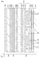
- FIG. 3 is a schematic partial plan view for explaining the plan shape of the light-shielding region in the liquid crystal display device.
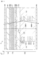
- FIG. 4 is a schematic partial plan view for explaining the planar shape of the light guide portion in the liquid crystal display device.
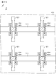
- FIG. 5 is a schematic partial plan view for explaining the planar shape of the polarizing element arranged between the light guide unit and the transparent pixel electrode in the liquid crystal display device.
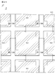
- FIG. 6 is a schematic partial plan view for explaining the planar shape of the transparent pixel electrode in the liquid crystal display device.
- FIG. 7 is a schematic cross-sectional view when the liquid crystal display device is cut at the portion shown by AA in FIG.
- FIG. 8 is a schematic cross-sectional view when the liquid crystal display device is cut at the portion shown by BB in FIG.
- FIG. 9 is a schematic cross-sectional view when the liquid crystal display device is cut at the portion shown by CC in FIG.
- FIG. 10 is a schematic partial cross-sectional view for explaining the state of light incident on the liquid crystal display device of the reference example.
- FIG. 11 is a schematic partial cross-sectional view for explaining the state of light passing through the light guide portion when the liquid crystal display device of the reference example is in the black display state.
- FIG. 7 is a schematic cross-sectional view when the liquid crystal display device is cut at the portion shown by AA in FIG.
- FIG. 8 is a schematic cross-sectional view when the liquid crystal display device
- FIG. 12 is a schematic partial cross-sectional view for explaining the state of light incident on the liquid crystal display device according to the first embodiment.
- FIG. 13 is a schematic partial plan view of a base material or the like for explaining the manufacturing method of the liquid crystal display device according to the first embodiment.
- FIG. 14 is a schematic partial plan view of a base material or the like for explaining the method of manufacturing the liquid crystal display device according to the first embodiment, following FIG. 13.
- FIG. 15 is a schematic partial plan view of a base material or the like for explaining a method of manufacturing a liquid crystal display device according to the first embodiment, following FIG.
- FIG. 16 is a schematic partial plan view of a base material or the like for explaining a method of manufacturing a liquid crystal display device according to the first embodiment, following FIG. FIG.
- FIG. 17 is a schematic partial plan view of a base material or the like for explaining a method of manufacturing a liquid crystal display device according to the first embodiment
- FIG. 18 is a schematic partial plan view of a base material or the like for explaining a method of manufacturing a liquid crystal display device according to the first embodiment
- FIG. 19 is a schematic partial plan view of a base material or the like for explaining a method of manufacturing a liquid crystal display device according to the first embodiment
- FIG. 20 is a schematic partial plan view of a base material or the like for explaining a method of manufacturing a liquid crystal display device according to the first embodiment, following FIG. 19.
- FIG. 19 is a schematic partial plan view of a base material or the like for explaining a method of manufacturing a liquid crystal display device according to the first embodiment, following FIG. 19.
- FIG. 19 is a schematic partial plan view of a base material or the like for explaining a method of manufacturing a liquid crystal display device according to the first embodiment, following FIG. 19.
- FIG. 19 is a schematic partial plan view of
- FIG. 21 is a schematic partial plan view of a base material or the like for explaining a method of manufacturing a liquid crystal display device according to the first embodiment, following FIG. 20.
- 22A and 22B are schematic partial cross-sectional views of a base material and the like for explaining the process of forming the light guide portion shown in FIG. 21.
- 23A and 23B are schematic partial cross-sectional views of a base material and the like for explaining the process of forming the light guide portion shown in FIG. 21, following FIG. 22B.
- FIG. 24 is a schematic partial plan view of a base material or the like for explaining the method of manufacturing the liquid crystal display device according to the first embodiment, following FIG. 21.
- FIG. 25A, 25B, 25C, 25D, 25E, and 25F are schematic partial cross-sectional views of a base material and the like for explaining the process of forming the polarizing element shown in FIG. 24.
- FIG. 26 is a schematic partial plan view of a base material or the like for explaining a method of manufacturing a liquid crystal display device according to the first embodiment, following FIG. 24.
- FIG. 27 is a schematic partial cross-sectional view of the liquid crystal display device according to the second embodiment of the present disclosure.
- FIG. 28 is a schematic partial plan view of a base material or the like for explaining the planar shape of the light guide portion of the liquid crystal display device according to the second embodiment.
- FIG. 29A and 29B are schematic partial cross-sectional views of a base material and the like for explaining the process of forming the light guide portion shown in FIG. 28.
- 30A and 30B are schematic partial cross-sectional views of a base material and the like for explaining the process of forming the light guide portion shown in FIG. 28, following FIG. 29B.
- FIG. 31 is a schematic partial cross-sectional view of the liquid crystal display device according to the third embodiment of the present disclosure.
- FIG. 32 is a conceptual diagram of a projection type display device.
- 33 is an external view of an interchangeable lens single-lens reflex type digital still camera, the front view thereof is shown in FIG. 33A, and the rear view thereof is shown in FIG. 24B.
- FIG. 34 is an external view of the head-mounted display.
- FIG. 35 is an external view of a see-through head-mounted display.
- the liquid crystal display device according to the present disclosure and the liquid crystal display device used for the electronic device according to the present disclosure may be simply referred to as “the liquid crystal display device of the present disclosure”.
- the electro-optic substrate according to the present disclosure and the electro-optic substrate used in the liquid crystal display device of the present disclosure may be simply referred to as "the electro-optic substrate of the present disclosure”.
- the electro-optical substrate of the present disclosure has a support base material and transparent pixel electrodes arranged in a matrix on the front side of the support base material, and a light guide unit corresponding to each transparent pixel electrode. Is provided on the back surface side of the transparent pixel electrode, and a polarizing element is arranged between the light guide portion and the transparent pixel electrode.
- the light guide includes a translucent material that extends in the normal direction with respect to the supporting substrate and whose wall surface is arranged so as to be in contact with a material having a relatively low refractive index.
- the light guide portion can be configured by providing an opening in the silicon oxide layer and embedding a silicon oxynitride in the opening.
- the material constituting the light guide portion and its surroundings is not particularly limited, and may be appropriately selected depending on the configuration of the electro-optical substrate.
- the light guide portion extends in the normal direction with respect to the supporting base material and includes a light-shielding material arranged so as to surround the wall surface of the translucent material located in the light guide region.
- the light-shielding material can be composed of aluminum (Al), an aluminum alloy such as Al—Cu or Al—Si, and a metal material such as silver (Ag).
- the polarizing element may be configured to consist of a wire grid polarizing element.
- the ratio of the transmittance in the transmission direction of the wire grid polarizing element to the transmittance in the direction orthogonal to the transmission direction is preferably 3 ⁇ 10 3 or more with respect to light having a wavelength of 550 nanometers.
- the wire grid polarizing element can be obtained by, for example, patterning a thin film of aluminum (Al) and appropriately covering it with a protective film.
- the stator can be configured to be electrically floating.
- the stator may be configured to apply a predetermined voltage.
- the stator may be configured such that the same voltage as that applied to the transparent pixel electrode is applied.
- the so-called common potential line (common potential line) and the polarizing element may be made conductive so that the common potential is supplied to the polarizing element.
- the electro-optical substrate of the present disclosure including the above-mentioned various preferable configurations may have a configuration in which yet another polarizing element is arranged on the back surface side of the supporting base material. For example, when the extinguishing ratio by the wire grid polarizing element is insufficient, the required extinguishing ratio can be secured by arranging another polarizing element.
- a substrate made of a transparent material such as glass or quartz can be used as the supporting base material used for the electro-optical substrate.
- the transparent pixel electrode and the counter electrode provided on the facing substrate can be formed by using a transparent conductive material such as indium tin oxide (ITO) or indium zinc oxide (IZO). In some cases, a metal film thin enough to have light transmission can be used.
- the counter electrode functions as a common electrode for each pixel of the liquid crystal display device.
- the thin film transistor constituting the switching element can be configured by forming and processing a semiconductor material layer or the like on the substrate.
- the materials constituting the various wirings and contacts used in the present disclosure are not particularly limited, and are, for example, aluminum (Al), aluminum alloys such as Al—Cu and Al—Si, tungsten (W), and tungsten silicide (WSi). Metallic materials such as tungsten alloys such as x) can be used.
- the insulating layer and the material constituting the insulating film used in the present disclosure are not particularly limited as long as they do not interfere with the implementation of the present disclosure.
- an inorganic material such as silicon oxide or an organic material such as polyimide can be used.
- the liquid crystal display device may be configured to display a monochrome image or may be configured to display a color image.
- pixel values of the liquid crystal display device in addition to U-XGA (1600,1200), HD-TV (1920,1080), Q-XGA (2048,1536), (3840,2160), (7680, Some of the image resolutions, such as 4320), can be exemplified, but are not limited to these values.
- various electronic devices having an image display function can be exemplified in addition to the direct-view type and projection type display devices.
- the first embodiment relates to an electro-optic substrate, a liquid crystal display device, and an electronic device according to the present disclosure.
- FIG. 1 is a schematic diagram for explaining a liquid crystal display device according to the first embodiment of the present disclosure.
- the liquid crystal display device is an active matrix type liquid crystal display device.
- the liquid crystal display device 1 includes various circuits such as pixels PX arranged in a matrix, a horizontal drive circuit 11 for driving the pixels PX, and a vertical drive circuit 12.
- the reference numeral SCL is a scanning line for scanning the pixel PX
- the reference numeral DTL is a signal line for supplying various voltages to the pixel PX.
- M pixels in the horizontal direction and N pixels in the vertical direction, for a total of M ⁇ N are arranged in a matrix.
- the counter electrode shown in FIG. 1 is provided as a common electrode for each liquid crystal cell.
- the horizontal drive circuit 11 and the vertical drive circuit 12 are respectively arranged on one end side of the liquid crystal display device 1, but this is merely an example.
- FIG. 2A is a schematic cross-sectional view for explaining the basic configuration of the liquid crystal display device.
- FIG. 2B is a schematic circuit diagram for explaining pixels in a liquid crystal display device.
- the liquid crystal display device 1 is An electro-optic substrate 100 having a support base material and transparent pixel electrodes arranged in a matrix on the front surface side of the support base material, and Opposing substrate 180 arranged so as to face the electro-optical substrate 100, and The liquid crystal material layer 170 enclosed between the electro-optic substrate 100 and the facing substrate 180, Includes.
- the electro-optic substrate 100 and the facing substrate 180 are sealed by a sealing portion 190.
- the sealing portion 190 is an annular shape surrounding the liquid crystal material layer 170.
- the liquid crystal display device 1 is a transmissive liquid crystal display device.
- the facing substrate 180 is provided with a facing electrode made of a transparent conductive material such as ITO. More specifically, the facing substrate 180 is composed of, for example, a rectangular substrate made of quartz glass, a counter electrode provided on the surface on the liquid crystal material layer 170 side, an alignment film provided on the counter electrode, and the like. There is. Further, a polarizing plate or the like is appropriately attached to the facing substrate 180. For convenience of illustration, the electro-optic substrate 100 and the facing substrate 180 in FIG. 2A are shown in a simplified manner.
- the liquid crystal cell constituting the pixel PX is composed of a transparent pixel electrode provided on the electro-optical substrate 100, a liquid crystal material layer of a portion corresponding to the transparent pixel electrode, and a counter electrode.
- a transparent pixel electrode provided on the electro-optical substrate 100
- a liquid crystal material layer of a portion corresponding to the transparent pixel electrode and a counter electrode.
- positive or negative common potentials V com are alternately applied to the counter electrodes when the liquid crystal display device 1 is driven.
- Each element of the pixel PX, excluding the liquid crystal material layer and the counter electrode, is formed on the electro-optic substrate 100 shown in FIG. 2A.
- one source / drain region of the thin film transistor TR is connected to the signal line DTL, and the other source / drain region is connected to one electrode of the transparent pixel electrode and the capacitance portion CS.
- the pixel voltage supplied from the signal line DTL is applied to the transparent pixel electrode via the thin film transistor TR which is made conductive by the scanning signal of the scanning line SCL. Since the transparent pixel electrode and one electrode of the capacitance portion CS are conducting, the pixel voltage is also applied to one electrode of the capacitance portion CS.
- a common potential V com is applied to the other electrode of the capacitive portion. In this configuration, the voltage of the transparent pixel electrode is held by the capacitance of the liquid crystal cell and the capacitance portion CS even after the thin film transistor TR is brought into a non-conducting state.
- the electro-optical substrate 100 is formed with a light guide portion corresponding to each transparent pixel electrode, and a polarizing element is arranged between the light guide portion and the transparent pixel electrode.
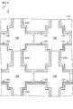
- FIG. 3 is a schematic partial plan view for explaining the plan shape of the light-shielding region in the liquid crystal display device.
- FIG. 4 is a schematic partial plan view for explaining the planar shape of the light guide portion in the liquid crystal display device.
- FIG. 5 is a schematic partial plan view for explaining the planar shape of the polarizing element arranged between the light guide unit and the transparent pixel electrode in the liquid crystal display device.
- FIG. 6 is a schematic partial plan view for explaining the planar shape of the transparent pixel electrode in the liquid crystal display device.
- various wirings and the like are formed on the electro-optical substrate 100.
- a light-shielding region is formed in the liquid crystal display device 1 by these various wirings.
- the hatched portion shows the planar shape of the light-shielding region SHA formed by various wirings and the like.
- the pixel opening region is provided in a region that does not overlap with the light-shielding region SHA.
- FIGS. 3 to 6 Since a large number of components are laminated on the electro-optic substrate 100, the legibility is impaired if all the components are shown on the plan view. Therefore, in FIGS. 3 to 6, only limited elements are displayed. The detailed arrangement relationship of each element will be described in detail with reference to FIGS. 7 to 9.
- a light guide unit LG is formed in a region that does not overlap with the light-shielding region SHA.
- the light guide unit LG includes a translucent material 140 which extends in the normal direction with respect to the supporting base material and whose wall surface is arranged so as to be in contact with a material having a relatively low refractive index.
- the hatched area in FIG. 4 indicates the area where the translucent material 140 is arranged.
- the polarizing element 150 shown in FIG. 5 is arranged above the light guide unit LG shown in FIG.
- the hatched region in FIG. 5 indicates a region in which the polarizing element 150 is arranged.
- the polarizing element 150 is composed of a wire grid polarizing element and is arranged corresponding to each light guide unit LG.
- the transparent pixel electrode 161 shown in FIG. 6 is arranged above the polarizing element 150.
- the hatched region in FIG. 6 indicates a region in which the transparent pixel electrode 161 is arranged.
- the transparent pixel electrode 161, the polarizing element 150, and the light guide unit LG are sequentially laminated. Therefore, the light incident on the transparent pixel electrode 161 via the liquid crystal material layer 170 first passes through the polarizing element 150 and then reaches the light guide unit LG. Therefore, the light reaches the light guide unit LG after passing through the polarizing element 150.
- the display state is not affected.
- FIG. 7 is a schematic cross-sectional view when the liquid crystal display device is cut at the portion shown by AA in FIG.
- FIG. 8 is a schematic cross-sectional view when the liquid crystal display device is cut at the portion shown by BB in FIG.
- FIG. 9 is a schematic cross-sectional view when the liquid crystal display device is cut at the portion shown by CC in FIG.
- the planar shape of each element will be described with reference to FIGS. 13 to 26 for explaining the manufacturing method of the liquid crystal display device 1.
- scanning lines 111 extending in the X direction in the figure (corresponding to SCL in FIG. 1) are placed on the support base material 101. It is formed.
- the hatched portion shows the planar shape of the scanning line 111.
- an insulating film 112 is formed on the entire surface including the scanning line 111, and a semiconductor material layer 121 constituting the thin film transistor TR is formed on the insulating film 112.
- the hatched portion shows the planar shape of the semiconductor material layer 121.
- a gate insulating film 122 is formed on the entire surface including the semiconductor material layer 121, and a gate electrode 124 is formed on the gate insulating film 122.
- the gate insulating film 122 and the insulating film 112 are provided with an opening in which the scanning line 111 is exposed, and a contact 123 between the gate electrode 124 and the scanning line 111 is formed in this portion. ..
- the hatched portion shows the planar shape of the gate electrode 124 and the contact 123.
- an insulating film 125 is formed on the entire surface including the gate electrode 124.
- a wiring layer 130 including a light-shielding film 131 located above the thin film transistor TR is formed on the insulating film 125.
- the wiring layer 130 is configured by laminating a plurality of material layers, and the laminated wiring, electrodes, and the like are separated by an insulating layer.
- various insulating layers constituting the wiring layer 130 may be represented by using reference numerals 130A.
- the light-shielding film 131 is formed of a conductive material having a light-shielding property. As shown in FIG. 9, the insulating film 125 and the gate insulating film 122 are provided with an opening in which the semiconductor material layer 121 is exposed, and a contact 126 is formed in this portion. The light-shielding film 131 conducts with the other source / drain region of the thin film transistor TR via the contact 126. A pixel voltage is applied to the light-shielding film 131 from the signal line via the thin film transistor TR in a conductive state.
- the hatched portion shows the planar shape of the light-shielding film 131 and the contact 126.
- the light-shielding film 131 is formed so as to cover the upper part of the thin film transistor TR.
- an electrode 132 is formed above the light-shielding film 131. As will be described later, a common potential is applied to the electrode 132 from a common potential line, and the electrode 132 functions as an electrode of the capacitance portion CS. In FIG. 17, the hatched portion shows the planar shape of the electrode 132.
- a signal line 134 (corresponding to DTL in FIG. 1) extending in the Y direction in the figure is formed above the electrode 132.
- the wiring layer 130, the insulating film 125, and the gate insulating film 122 are provided with an opening in which the semiconductor material layer 121 is exposed, and a contact 133 is formed in this portion.
- the signal line 134 conducts with one source / drain region of the thin film transistor TR via the contact 133.
- the hatched portion shows the planar shape of the signal line 134 and the contact 133.
- a common potential line 136 extending in the Y direction in the figure is formed above the signal line 134.
- the wiring layer 130 is provided with an opening in which the electrode 132 is exposed, and a contact 135 is formed in this portion.
- the common potential line 136 conducts with the electrode 132 via the contact 135.
- the capacitance portion CS is formed by the electrode 132 and the light-shielding film 131.
- the hatched portion shows the planar shape of the common potential line 136 and the contact 135.
- a relay electrode 138 is formed above the common potential line 136.
- the wiring layer 130 is provided with an opening in which the light-shielding film 131 is exposed, and a contact 137 is formed in this portion.
- the relay electrode 138 conducts with the light-shielding film 131 via the contact 137.
- the hatched portion shows the planar shape of the relay electrode 138 and the contact 137.
- the light-shielding region SHA shown in FIG. 3 is formed by the various wirings and electrodes described above.
- the light guide portion LG shown in FIG. 7 is formed in a region that does not overlap with the light-shielding region SHA.
- the light guide portion LG extends in the normal direction (Z direction in the figure) with respect to the support base material 101, and is a translucent material whose wall surface is arranged so as to be in contact with a material having a relatively low refractive index.
- Contains 140 140.
- the translucent material 140 is formed of silicon oxynitride, and its wall surface is embedded so as to be in contact with a silicon oxide having a relatively low refractive index. Therefore, the light incident on the wall surface of the translucent material 140 exceeding the critical angle is totally reflected.
- the translucent material 140 is formed by engraving the support base material 101 and the wiring layer 130, and is formed so that the end surface is substantially the same as the surface of the relay electrode 138. In FIG. 21, the hatched area indicates the area where
- an insulating film as a surface layer of the wiring layer 130 is formed on the entire surface including the relay electrode 138.
- a transparent pixel electrode 161 formed by dividing a transparent conductive material film into a two-dimensional matrix at a predetermined pitch is formed on the insulating film.
- Reference numeral 139 shown in FIG. 8 indicates the contact between the transparent pixel electrode 161 and the relay electrode 138.
- the pixel voltage held by the capacitance unit CS is supplied to the transparent pixel electrode 161 via the contact 139.
- the hatched portion shows the planar shape of the transparent pixel electrode 161 and the contact 139.
- a flattening film 162 is formed on the entire surface including the transparent pixel electrode 161 and an alignment film 163 is formed on the flattening film 162.
- a polarizing element 150 is arranged between the transparent pixel electrode 161 and the light guide unit LG.
- the polarizing element 150 is composed of a wire grid polarizing element.
- the wire grid modulator is composed of a large number of nano-order metal wires arranged in parallel, transmits an electric field vector perpendicular to the metal wire, and reflects an electric field vector parallel to the metal wire. Therefore, since the wire grid splitter does not absorb light, it also has excellent heat resistance.
- the hatched region indicates a region in which the polarizing element 150 is arranged.
- the ratio of the transmittance of the polarizing element 150 in the transmission direction and the transmittance in the direction orthogonal to the transmission direction is 3 ⁇ 10 3 with respect to light having a wavelength of 550 nanometers. It is preferable to have the above configuration.
- the polarizing element 150 is electrically floating, but the present invention is not limited to this.
- a predetermined voltage may be applied to the polarizing element 150.
- the voltage of the common potential line 136 is applied to the polarizing element 150 by forming necessary contacts as appropriate, or the same voltage as the voltage applied to the transparent pixel electrode 161 by conducting the polarizing element 150 and the relay electrode 138 is applied. It can also be configured to be applied.
- the facing substrate 180 arranged to face the electro-optical substrate 100 is provided on a rectangular base material 181 made of, for example, quartz glass and a surface on the liquid crystal material layer 170 side. It includes an alignment film 183 provided on the counter electrode 182 and the counter electrode 182, and further includes a polarizing element 184 arranged on the base material 181.
- the polarizing element 184 and the polarizing element 150 provided on the electro-optical substrate 100 are arranged in a state in which the polarization axes are orthogonal to each other (cross Nicol).
- the configuration of the polarizing element 184 is not particularly limited, and may be an absorption type polarizing element or a wire grid polarizing element. When heat resistance is required, it is preferable to use the polarizing element 184 as a wire grid polarizing element.
- the liquid crystal material layer 170 is sandwiched between the alignment film 163 of the electro-optical substrate 100 and the alignment film 183 of the facing substrate 180.
- the orientation state of the liquid crystal molecules 171 when there is no electric field is defined by the alignment films 163 and 183.
- the liquid crystal display device 1 is, for example, a vertically oriented (VA) type liquid crystal display device.
- FIG. 10 is a schematic partial cross-sectional view for explaining the state of light incident on the liquid crystal display device of the reference example.
- the liquid crystal display device 9 of the reference example has a configuration in which the polarizing element 150 of the liquid crystal display device 1 is omitted and the polarizing element 950 is arranged on the back surface of the supporting base material 101.
- the extruder 950 and the stator 184 are arranged in a cross-nicol state.
- the light incident on the liquid crystal display device 9 from the light source unit (not shown) is not completely parallel light, but has an angle in the range of, for example, about ⁇ 10 degrees.
- the light incident on the facing substrate 180 passes through the light guide unit LG as it is (light ray A shown in FIG. 10) and when it passes after being totally reflected by the wall surface of the light guide unit LG (light ray B shown in FIG. 10). There is.
- a phase shift called a goose-henshen shift occurs in the light reflected at the interface or the like. Therefore, there is a phase difference between the light ray A that passes through the waveguide without being reflected and the light ray B that is reflected and passed through at the interface or the like.
- FIG. 11 is a schematic partial cross-sectional view for explaining the state of light passing through the light guide unit when the liquid crystal display device of the reference example is in the black display state.
- the liquid crystal material layer 170 does not cause a phase difference with respect to the transmitted light. Since the polarizing element 184 and the polarizing element 950 are in the cross Nicol state, it is desirable that neither the light ray A nor the light ray B passing through the light guide unit LG passes through the polarizing element 950 as a black display state. However, the phase of the light ray B changes with respect to the light ray A due to the phase shift due to reflection. Therefore, a part of the light ray B passes through the polarizing element 950. This is a factor that reduces the contrast of the displayed image.
- phase of the light ray B changes with respect to the light ray A causes a deviation from the originally intended brightness even in the display state of the liquid crystal display device 9.
- Degradation of contrast and deviation from the originally intended brightness are factors that impair the quality of the displayed image.
- the polarizing element 150 is arranged between the transparent pixel electrode 161 and the light guide unit LG.
- FIG. 12 is a schematic partial cross-sectional view for explaining the state of light incident on the liquid crystal display device according to the first embodiment.
- the light incident on the facing substrate 180 passes through the polarizing element 150 and then reaches the light guide unit LG. Therefore, when the liquid crystal display device 1 is in the black display state, neither the light rays A nor the light rays B pass through the polarizing element 150. Therefore, unlike the liquid crystal display device 9, the intended black display state can be obtained. Further, when the liquid crystal display device 1 is in the white display state, both the light rays A and the light rays B pass through the polarizing element 150 and reach the light guide unit LG. Then, the light ray B causes a phase shift, which does not affect the display state. As described above, in the display device 1, the phase shift of the light reflected at the interface or the like does not affect the display state.
- the stray light incident on the transistor can be reduced. Thereby, the leakage of the transistor can be reduced.
- FIGS. 13 to 21, 24 and 26 are schematic plan views, but from the viewpoint of legibility, the display of the insulating layer and the insulating film is omitted in these views.
- the manufacturing method of the liquid crystal display device 1 will be described in detail.
- Step-100 (see FIGS. 8, 9, 13, 14, 14 and 15).
- a scanning line is formed on the supporting substrate.
- a support base material 101 is prepared, and scanning lines 111 are formed on the support base material 101 by a well-known film forming method or patterning method (see FIG. 13).
- the scanning line 111 is made of a metal material such as tungsten (W) or Al—Cu. The same applies to other wirings and electrodes described later.
- a thin film transistor TR is formed above the scanning line 111.
- An insulating film 112 made of, for example, a silicon oxide is formed on the entire surface including the scanning line 111, and a semiconductor material layer 121 constituting the thin film transistor TR is formed on the insulating film 112 by a well-known film forming method or patterning method (FIG. 14). reference).
- a gate insulating film 122 made of, for example, a silicon oxide is formed on the entire surface including the semiconductor material layer 121.
- an opening is provided in the gate insulating film 122 and the insulating film 112 in the portion corresponding to the contact 123.
- a conductive material is embedded in the opening to form the contact 123, and then the gate electrode 124 is formed by a well-known film forming method or patterning method (see FIG. 15).
- the thin film transistor TR is formed above the scanning line 111.
- an insulating film 125 made of, for example, a silicon oxide is formed on the entire surface including the gate electrode 124.
- Step-110 (see FIGS. 8, 9, 16 and 17) After that, the light-shielding film 131 is formed above the thin film transistor TR. First, an opening is provided in the insulating film 125 or the like corresponding to the contact 126 to expose the semiconductor material layer 121. Next, a conductive material is embedded in the opening to form the contact 126, and then the light-shielding film 131 is formed by a well-known film forming method or patterning method (see FIG. 16). The light-shielding film 131 is connected to the semiconductor material layer 121 via the contact 126 (see FIG. 9).
- the electrode 132 constituting the capacitance portion CS is formed above the light-shielding film 131.
- An insulating layer made of, for example, a silicon oxide is formed on the entire surface including the light-shielding film 131, and then an electrode 132 is formed on the insulating layer by a well-known film forming method or patterning method (see FIG. 17).
- a signal line 134 is formed above the electrode 132.
- an insulating layer made of, for example, a silicon oxide on the entire surface including the electrode 132, an opening is provided in a portion corresponding to the contact 133 to expose the semiconductor material layer 121.
- a conductive material is embedded in the opening to form the contact 133, and then the signal line 134 is formed by a well-known film forming method or patterning method (see FIG. 18).
- the signal line 134 is connected to the semiconductor material layer 121 via the contact 133 (see FIG. 9).
- a common potential line 136 is formed above the signal line 134.
- an insulating layer made of, for example, a silicon oxide on the entire surface including the signal line 134, an opening is provided in a portion corresponding to the contact 135 to expose the electrode 132.
- a conductive material is embedded in the opening to form the contact 135, and then the common potential line 136 is formed by a well-known film forming method or patterning method (see FIG. 19).
- the common potential line 136 is connected to the electrode 132 via the contact 135 (see FIG. 8).
- Step-130 (see FIGS. 8, 9, and 20)
- the relay electrode 138 is formed above the common potential line 136.
- an insulating layer made of, for example, a silicon oxide on the entire surface including the common potential line 136
- an opening is provided in a portion corresponding to the contact 137 to expose the light-shielding film 131.
- a conductive material is embedded in the opening to form the contact 137, and then the relay electrode 138 is formed by a well-known film forming method or patterning method (see FIG. 20).
- the relay electrode 138 is connected to the light-shielding film 131 via the contact 137 (see FIG. 8).
- Step-140 (see FIGS. 7, 21, 22A, 22B, 23A and 23B).
- the light guide unit LG is formed.
- An insulating layer made of, for example, a silicon oxide is formed on the entire surface including the relay electrode 138, and then flattened so that the relay electrode 138 is exposed (see FIG. 22A).
- an opening OP is provided in the portion to be embedded with the translucent material 140 shown in FIG. 21 (see FIG. 22B).
- a silicon oxynitride is formed on the entire surface of the translucent material 140 to embed the inside of the opening OP (see FIG. 23A). Then, for example, flattening is performed so that the relay electrode 138 is exposed. After that, an insulating film 130A made of, for example, a silicon oxide is formed on the entire surface (see FIG. 23B). By the above steps, the light guide unit LG can be obtained.
- Step-150 (see FIGS. 7, 24, 25A, 25B, 25C, 25D, 25E and 25F).
- the polarizing element 150 is formed above the light guide unit LG.
- a metal film 151A made of, for example, aluminum (Al) is formed on the insulating film 130A (see FIG. 25A).
- a resist is patterned on the resist to form a mask 152 (see FIG. 25B).
- the metal film 151A is patterned by using, for example, a dry etching method, and a large number of nano-order metal wires 151 are arranged in parallel in the region indicated by reference numeral 150 in FIG. 24 (see FIG. 25C).
- the mask 152 is removed (FIG. 25D), and then a protective film 153 made of, for example, a silicon oxide is formed (FIG. 25E).
- a protective film 153 made of, for example, a silicon oxide is formed (FIG. 25E).
- the polarizing element 150 can be formed.
- the extinction ratio of the wire grid polarizing element increases as the refractive index of the substance between the wire grids decreases. Therefore, for example, as shown in FIG. 25F, the protective film 153 may be formed so that a void 154 is formed between the metal wire 151 and the metal wire 151.
- the transparent pixel electrode 161 is formed above the polarizing element 150.
- an opening is provided in a portion corresponding to the contact 139 to expose the relay electrode 138.
- a conductive material is embedded in the opening to form the contact 138, and then the transparent pixel electrode 161 is formed by a well-known film forming method or patterning method (see FIG. 26).
- the transparent pixel electrode 161 is connected to the light-shielding film 131 constituting the electrode of the capacitance portion CS via the contact 139, the relay electrode 138, and the contact 137.
- a flattening film 162 made of, for example, a silicon oxide is formed on the entire surface including the transparent pixel electrode 161 and then an alignment film 163 is further formed.
- the electro-optical substrate 100 used in the liquid crystal display device 1 can be obtained.
- a facing substrate 180 having a rectangular base material 181 made of, for example, quartz glass, a counter electrode 182 provided on one surface of the base material 181 and an alignment film 183 provided on the facing electrode 182 is prepared. do. Then, the electro-optic substrate 100 and the facing substrate 180 are opposed to each other with the liquid crystal material layer 170 sandwiched therein, and the periphery is sealed. After that, the liquid crystal display device 1 can be obtained by arranging the polarizing element 184 on the other surface of the base material 181.
- the second embodiment also relates to an electro-optic substrate, a liquid crystal display device, and an electronic device according to the present disclosure.
- FIG. 27 is a schematic partial cross-sectional view of the liquid crystal display device according to the second embodiment of the present disclosure, and is a drawing corresponding to FIG. 7 referred to in the first embodiment.
- the liquid crystal display device 1 may be read as the liquid crystal display device 2 in FIG.
- the light guide portion extends in the normal direction with respect to the supporting base material and is arranged so as to surround the wall surface of the translucent material located in the light guide region. It contained a light-shielding material.
- the light guide portion extends in the normal direction with respect to the support base material and has a wall surface of a translucent material located in the light guide region. The difference is that it contains a light-shielding material arranged so as to surround it.
- FIG. 28 is a schematic partial plan view of a base material or the like for explaining the planar shape of the light guide portion of the liquid crystal display device according to the second embodiment.
- the light guide portion LG extends in the normal direction with respect to the support base material 101 and surrounds the wall surface of the translucent material located in the light guide region.
- a light-shielding material 240 located in.
- the light-shielding material 240 is made of a metal material such as aluminum (Al) or silver (Ag).
- Al aluminum
- Ag silver
- FIG. 28 in the region surrounded by the light-shielding material 240, the same material as the material constituting the insulating layer used for the wiring layer 130, for example, silicon oxide is embedded.
- the light incident on the facing substrate 180 reaches the light guide unit LG after passing through the polarizing element 150.
- the light reflected by the light-shielding material 240 of the light guide unit LG causes a phase shift, which affects the display state as described with reference to FIG. 12 in the first embodiment. There is no such thing.
- the thin film transistor TR is located outside the region surrounded by the light-shielding material 240. Therefore, the stray light incident on the thin film transistor TR can be reduced. Thereby, the leakage of the thin film transistor TR can be reduced.
- 29 and 30 are various drawings for explaining the manufacturing method of the liquid crystal display device 2.
- Step-210 (see FIGS. 28, 29A, 29B, 30A and 30B).
- the light guide unit LG is formed.
- An insulating layer made of, for example, a silicon oxide is formed on the entire surface including the relay electrode 138, and then flattened so that the relay electrode 138 is exposed, for example.
- an opening OP is provided so that the wall surface forming the light-shielding material 240 shown in FIG. 28 is exposed (see FIG. 29A).
- a light-shielding material 240 is formed on the wall surface of the opening OP (see FIG. 29B).
- an insulating film 130A made of, for example, a silicon oxide is formed on the entire surface to fill the inside of the opening (see FIG. 30A). Then, for example, flattening is performed so that the relay electrode 138 is not exposed (see FIG. 30B). By the above steps, the light guide unit LG can be obtained.
- a third embodiment also relates to an electro-optic substrate, a liquid crystal display device, and an electronic device according to the present disclosure.
- FIG. 31 is a schematic partial cross-sectional view of the liquid crystal display device according to the third embodiment of the present disclosure, and is a drawing corresponding to FIG. 7 referred to in the first embodiment.
- the liquid crystal display device 1 may be read as the liquid crystal display device 3 in FIG.
- the polarizing element of the electro-optical substrate 100 is arranged between the transparent pixel electrode and the light guide unit.
- the liquid crystal display device 3 according to the third embodiment is different in that yet another polarizing element is arranged on the back surface side of the supporting base material of the electro-optical substrate. Except for the above points, the configuration is the same as that of the liquid crystal display device 1.
- the liquid crystal display device 2 described in the second embodiment may also have a configuration in which another polarizing element 350 is arranged on the back surface side of the support base material 101 of the electro-optical substrate 200.
- the configuration of the polarizing element 350 is not particularly limited, and may be an absorption type polarizing element or a wire grid polarizing element. When heat resistance is required, it is preferable to use the polarizing element 350 as a wire grid polarizing element.
- the liquid crystal display device is a display unit (display device) of an electronic device in all fields for displaying a video signal input to an electronic device or a video signal generated in the electronic device as an image or a video.
- a display unit such as a television set, a digital still camera, a notebook personal computer, a portable terminal device such as a mobile phone, a video camera, and a head mount display (head-mounted display).
- the liquid crystal display device of the present disclosure also includes a modular one having a sealed configuration.
- a display module formed by attaching a facing portion such as a transparent glass material to a pixel array portion is applicable.
- the display module may be provided with a circuit unit for inputting / outputting a signal or the like from the outside to the pixel array unit, a flexible printed circuit (FPC), or the like.
- FPC flexible printed circuit
- FIG. 32 is a conceptual diagram of a projection type display device using the liquid crystal display device of the present disclosure.
- the projection type display device includes a light source unit 400, an illumination optical system 410, a liquid crystal display device 1, an image control circuit 420 for driving the liquid crystal display device, a projection optical system 430, a screen 440, and the like.
- the light source unit 400 can be composed of, for example, various lamps such as xenon lamps and semiconductor light emitting elements such as light emitting diodes.
- the illumination optical system 410 is used to guide the light from the light source unit 400 to the liquid crystal display device 1, and is composed of optical elements such as a prism and a dichroic mirror.
- the liquid crystal display device 1 acts as a light bulb, and an image is projected on the screen 440 via the projection optical system 430.
- the interchangeable-lens single-lens reflex type digital still camera has, for example, an interchangeable photographing lens unit (interchangeable lens) 512 on the front right side of the camera body (camera body) 511, and is held by the photographer on the front left side. It has a grip portion 513 for the purpose.
- interchangeable photographing lens unit interchangeable lens
- a monitor 514 is provided in the center of the back of the camera body 511.
- a viewfinder (eyepiece window) 515 is provided on the upper part of the monitor 514. By looking into the viewfinder 515, the photographer can visually recognize the optical image of the subject guided from the photographing lens unit 512 and determine the composition.
- the liquid crystal display device of the present disclosure can be used as the viewfinder 515. That is, the interchangeable lens type single-lens reflex type digital still camera according to this example is manufactured by using the liquid crystal display device of the present disclosure as its viewfinder 515.
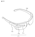
- FIG. 34 is an external view of the head-mounted display.
- the head-mounted display has, for example, ear hooks 612 for being worn on the user's head on both sides of the eyeglass-shaped display unit 611.
- the liquid crystal display device of the present disclosure can be used as the display unit 611. That is, the head-mounted display according to this example is manufactured by using the liquid crystal display device of the present disclosure as the display unit 611.
- FIG. 35 is an external view of a see-through head-mounted display.
- the see-through head-mounted display 711 is composed of a main body portion 712, an arm 713, and a lens barrel 714.
- the main body 712 is connected to the arm 713 and the glasses 700. Specifically, the end portion of the main body portion 712 in the long side direction is connected to the arm 713, and one side of the side surface of the main body portion 712 is connected to the eyeglasses 700 via a connecting member.
- the main body portion 712 may be directly attached to the head of the human body.
- the main body 712 incorporates a control board for controlling the operation of the see-through head-mounted display 711 and a display unit.
- the arm 713 connects the main body 712 and the lens barrel 714, and supports the lens barrel 714. Specifically, the arm 713 is coupled to the end of the main body 712 and the end of the lens barrel 714, respectively, to fix the lens barrel 714. Further, the arm 713 has a built-in signal line for communicating data related to an image provided from the main body portion 712 to the lens barrel 714.
- the lens barrel 714 projects the image light provided from the main body 712 via the arm 713 toward the eyes of the user who wears the see-through head-mounted display 711 through the eyepiece.
- the liquid crystal display device of the present disclosure can be used for the display unit of the main body unit 712.
- A1 It has a support base material and transparent pixel electrodes arranged in a matrix on the front side of the support base material.
- a light guide unit corresponding to each transparent pixel electrode is provided on the back surface side of the transparent pixel electrode.
- a polarizing element is arranged between the light guide unit and the transparent pixel electrode.
- Electro-optic substrate [A2] The light guide extends in the normal direction with respect to the supporting substrate and contains a translucent material whose wall surface is arranged so as to be in contact with a material having a relatively low refractive index.
- the electro-optic substrate according to the above [A1].
- the light guide extends in the normal direction with respect to the supporting substrate and includes a light shielding material arranged so as to surround the wall surface of the translucent material located in the light guide region.
- the electro-optic substrate according to the above [A1].
- the light-shielding material consists of a metallic material, The electro-optic substrate according to the above [A3].
- the modulator consists of a wire grid modulator, The electro-optical substrate according to any one of the above [A1] to [A4].
- the ratio of the transmittance of the transducer in the transmission direction to the transmittance in the direction orthogonal to the transmission direction is 3 ⁇ 10 3 or more with respect to light having a wavelength of 550 nanometers.
- the transducer is electrically floating, The electro-optic substrate according to the above [A5].
- a predetermined voltage is applied to the splitter, The electro-optic substrate according to the above [A5].
- A9] The same voltage as that applied to the transparent pixel electrode is applied to the polarizing element.
- Yet another substituent is placed on the back side of the supporting substrate, The electro-optical substrate according to any one of the above [A1] to [A9].
- An electro-optic substrate having a support base material and transparent pixel electrodes arranged in a matrix on the front side of the support base material, Opposing boards arranged to face the electro-optic board, A liquid crystal material layer enclosed between the electro-optic substrate and the facing substrate, Includes A light guide unit corresponding to each transparent pixel electrode is provided on the back surface side of the transparent pixel electrode. A polarizing element is arranged between the light guide unit and the transparent pixel electrode. Liquid crystal display device. [B2] The light guide extends in the normal direction with respect to the supporting substrate and contains a translucent material whose wall surface is arranged so as to be in contact with a material having a relatively low refractive index. The liquid crystal display device according to the above [B1].
- the light guide extends in the normal direction with respect to the supporting substrate and includes a light shielding material arranged so as to surround the wall surface of the translucent material located in the light guide region.
- the light-shielding material consists of a metallic material, The liquid crystal display device according to the above [B3].
- the modulator consists of a wire grid modulator, The liquid crystal display device according to any one of the above [B1] to [B4].
- the ratio of the transmittance of the transducer in the transmission direction to the transmittance in the direction orthogonal to the transmission direction is 3 ⁇ 10 3 or more with respect to light having a wavelength of 550 nanometers.
- the liquid crystal display device according to the above [B5].
- the transducer is electrically floating, The liquid crystal display device according to the above [B5].
- a predetermined voltage is applied to the splitter, The liquid crystal display device according to the above [B5].
- B9 The same voltage as that applied to the transparent pixel electrode is applied to the polarizing element.
- the liquid crystal display device according to the above [B8].
- Yet another substituent is placed on the back side of the supporting substrate, The liquid crystal display device according to any one of the above [B1] to [B9].
- An electro-optic substrate having a support base material and transparent pixel electrodes arranged in a matrix on the front side of the support base material, Opposing boards arranged to face the electro-optic board, A liquid crystal material layer enclosed between the electro-optic substrate and the facing substrate, Includes A light guide unit corresponding to each transparent pixel electrode is provided on the back surface side of the transparent pixel electrode. A polarizing element is arranged between the light guide unit and the transparent pixel electrode. An electronic device equipped with a liquid crystal display device. [C2] The light guide extends in the normal direction with respect to the supporting substrate and contains a translucent material whose wall surface is arranged so as to be in contact with a material having a relatively low refractive index.
- the electronic device according to the above [C1].
- the light guide extends in the normal direction with respect to the supporting substrate and includes a light shielding material arranged so as to surround the wall surface of the translucent material located in the light guide region.
- the electronic device according to the above [C1].
- the light-shielding material consists of a metallic material, The electronic device according to the above [C3].
- the modulator consists of a wire grid modulator, The electronic device according to any one of the above [C1] to [C4].
- the ratio of the transmittance of the transducer in the transmission direction to the transmittance in the direction orthogonal to the transmission direction is 3 ⁇ 10 3 or more with respect to light having a wavelength of 550 nanometers.
- the transducer is electrically floating, The electronic device according to the above [C5].
- a predetermined voltage is applied to the splitter, The electronic device according to the above [C5].
- [C9] The same voltage as that applied to the transparent pixel electrode is applied to the polarizing element.
- [C10] Yet another substituent is placed on the back side of the supporting substrate, The electronic device according to any one of the above [C1] to [C9].
- Electro-optical substrate 101 ... Support substrate, 111 ... Scanning line, 112 ... insulating film, 121 ... semiconductor material layer, 122 ... gate insulating film, 123 ... contact, 124 ... gate electrode, 125 ... insulating film, 126 ... Contact, 130 ... wiring layer, 130A ... various insulating layers constituting the wiring layer, 131 ... light-shielding film, 132 ... electrode 133 ... contact, 134 ... signal line, 135 ... Contact, 136 ... Common potential line, 137 ... Contact, 138 ... Relay electrode, 139 ... Contact, 150 ...
- Polarizer 151A ... Metal film, 151 ... Wire grid, 152 ... Mask, 153 ... Protective film, 154 ... Void, 161 ... Transparent pixel electrode, 162 ... Flattening film, 163 ... Alignment film, 170 ... Liquid crystal Material layer, 171 ... liquid crystal molecule, 180 ... opposed substrate, 181 ... base material, 182 ... opposed electrode, 183 ... alignment film, 184 ... polarizing element, SHA ... shading Region, LG ... light guide unit, SCL ... scanning line, DTL ... signal line, PX ... pixel, TR ... thin film, CS ... capacitive part, 200 ... electro-optical substrate , 240 ...
- Light-shielding material 300 ... Electro-optical substrate, 350 ... Polarizer, 950 ... Polarizer, 400 ...
- Light source unit 410 ... Illumination optical system, 420 ... Image control circuit, 430 ... Projection optical system, 440 ... Screen, 511 ... Camera body, 512 ... Shooting lens unit, 513 ... Grip, 514 ... Monitor, 515 ... -Viewfinder, 611 ... optics-shaped display, 612 ... ear hook, 700 ... glasses, 711 ... see-through head mount display, 712 ... main body, 713 ... arm, 714 ... lens barrel
Landscapes
- Physics & Mathematics (AREA)
- Nonlinear Science (AREA)
- Mathematical Physics (AREA)
- Chemical & Material Sciences (AREA)
- Crystallography & Structural Chemistry (AREA)
- General Physics & Mathematics (AREA)
- Optics & Photonics (AREA)
- Geometry (AREA)
- Liquid Crystal (AREA)
Priority Applications (3)
| Application Number | Priority Date | Filing Date | Title |
|---|---|---|---|
| JP2022527616A JP7596375B2 (ja) | 2020-05-25 | 2021-04-28 | 電気光学基板、液晶表示装置および電子機器 |
| US17/998,786 US12050384B2 (en) | 2020-05-25 | 2021-04-28 | Electrooptic substrate, liquid crystal display device, and electronic apparatus |
| CN202180036865.1A CN115668044A (zh) | 2020-05-25 | 2021-04-28 | 电光基板、液晶显示装置和电子设备 |
Applications Claiming Priority (2)
| Application Number | Priority Date | Filing Date | Title |
|---|---|---|---|
| JP2020090254 | 2020-05-25 | ||
| JP2020-090254 | 2020-05-25 |
Publications (1)
| Publication Number | Publication Date |
|---|---|
| WO2021241127A1 true WO2021241127A1 (ja) | 2021-12-02 |
Family
ID=78744451
Family Applications (1)
| Application Number | Title | Priority Date | Filing Date |
|---|---|---|---|
| PCT/JP2021/017073 Ceased WO2021241127A1 (ja) | 2020-05-25 | 2021-04-28 | 電気光学基板、液晶表示装置および電子機器 |
Country Status (4)
| Country | Link |
|---|---|
| US (1) | US12050384B2 (https=) |
| JP (1) | JP7596375B2 (https=) |
| CN (1) | CN115668044A (https=) |
| WO (1) | WO2021241127A1 (https=) |
Citations (7)
| Publication number | Priority date | Publication date | Assignee | Title |
|---|---|---|---|---|
| JPH05241514A (ja) * | 1992-02-27 | 1993-09-21 | Sharp Corp | 表示装置 |
| JP2003107505A (ja) * | 2001-10-01 | 2003-04-09 | Semiconductor Energy Lab Co Ltd | 液晶表示装置および電子機器 |
| JP2007171802A (ja) * | 2005-12-26 | 2007-07-05 | Seiko Epson Corp | 液晶装置、及び投射型表示装置 |
| JP2010134270A (ja) * | 2008-12-05 | 2010-06-17 | Sony Corp | カラー液晶表示装置組立体、光変換装置、発光粒子積層構造体、及び、発光粒子積層構造体の形成方法 |
| JP2015197578A (ja) * | 2014-04-01 | 2015-11-09 | セイコーエプソン株式会社 | 液晶装置及び電子機器 |
| US9423646B2 (en) * | 2013-04-18 | 2016-08-23 | Samsung Display Co., Ltd. | Display device |
| WO2019235046A1 (ja) * | 2018-06-05 | 2019-12-12 | ソニーセミコンダクタソリューションズ株式会社 | 液晶表示装置及び投射型表示装置 |
Family Cites Families (2)
| Publication number | Priority date | Publication date | Assignee | Title |
|---|---|---|---|---|
| CN105700268A (zh) * | 2016-04-08 | 2016-06-22 | 武汉华星光电技术有限公司 | 液晶透镜及3d显示装置 |
| JP6536619B2 (ja) | 2017-04-26 | 2019-07-03 | セイコーエプソン株式会社 | 電気光学装置、透過型液晶表示装置および電子機器 |
-
2021
- 2021-04-28 WO PCT/JP2021/017073 patent/WO2021241127A1/ja not_active Ceased
- 2021-04-28 CN CN202180036865.1A patent/CN115668044A/zh active Pending
- 2021-04-28 US US17/998,786 patent/US12050384B2/en active Active
- 2021-04-28 JP JP2022527616A patent/JP7596375B2/ja active Active
Patent Citations (7)
| Publication number | Priority date | Publication date | Assignee | Title |
|---|---|---|---|---|
| JPH05241514A (ja) * | 1992-02-27 | 1993-09-21 | Sharp Corp | 表示装置 |
| JP2003107505A (ja) * | 2001-10-01 | 2003-04-09 | Semiconductor Energy Lab Co Ltd | 液晶表示装置および電子機器 |
| JP2007171802A (ja) * | 2005-12-26 | 2007-07-05 | Seiko Epson Corp | 液晶装置、及び投射型表示装置 |
| JP2010134270A (ja) * | 2008-12-05 | 2010-06-17 | Sony Corp | カラー液晶表示装置組立体、光変換装置、発光粒子積層構造体、及び、発光粒子積層構造体の形成方法 |
| US9423646B2 (en) * | 2013-04-18 | 2016-08-23 | Samsung Display Co., Ltd. | Display device |
| JP2015197578A (ja) * | 2014-04-01 | 2015-11-09 | セイコーエプソン株式会社 | 液晶装置及び電子機器 |
| WO2019235046A1 (ja) * | 2018-06-05 | 2019-12-12 | ソニーセミコンダクタソリューションズ株式会社 | 液晶表示装置及び投射型表示装置 |
Also Published As
| Publication number | Publication date |
|---|---|
| JPWO2021241127A1 (https=) | 2021-12-02 |
| US12050384B2 (en) | 2024-07-30 |
| CN115668044A (zh) | 2023-01-31 |
| JP7596375B2 (ja) | 2024-12-09 |
| US20230168547A1 (en) | 2023-06-01 |
Similar Documents
| Publication | Publication Date | Title |
|---|---|---|
| US7911571B2 (en) | Electro-optic device, electronic instrument, and projection display | |
| CN101533185B (zh) | 液晶显示装置及电子设备 | |
| CN110767729B (zh) | 显示装置及电子设备 | |
| CN112313567B (zh) | 显示装置、嵌入有显示装置的电子设备以及存储介质 | |
| JP3205767B2 (ja) | 透過型液晶表示装置 | |
| CN110618557A (zh) | 一种显示面板和显示装置 | |
| CN113242994B (zh) | 嵌入有摄像头以及显示装置的电子设备 | |
| WO2021024621A1 (ja) | トランジスタアレイ基板およびトランジスタアレイ基板の製造方法、並びに、液晶表示装置および電子機器 | |
| JP2011257638A (ja) | 表示装置 | |
| CN101726883B (zh) | 电光装置及电子设备 | |
| JP7596375B2 (ja) | 電気光学基板、液晶表示装置および電子機器 | |
| JP2011191475A (ja) | 電気光学装置及びその製造方法、並びに電子機器 | |
| JP2008203711A (ja) | アクティブマトリクス基板、電気光学装置及び電子機器 | |
| JPH07218901A (ja) | 液晶表示装置 | |
| JP2022055778A (ja) | 電気光学装置および電子機器 | |
| JP4254092B2 (ja) | 液晶表示パネルおよび電子機器 | |
| JP5374875B2 (ja) | 電気光学基板、電気光学装置、電気光学基板の設計方法及び電子機器 | |
| CN114815375B (zh) | 液晶显示面板及液晶显示装置 | |
| JP7415725B2 (ja) | 液晶装置、及び電子機器 | |
| US10558070B2 (en) | Transmissive-type liquid crystal display device and electronic apparatus | |
| JP2009122309A (ja) | 電気光学装置の製造方法及び電気光学装置、並びに電子機器 | |
| KR101041612B1 (ko) | 마이크로랜즈를 가지는 액정표시장치 및 그 제조방법 | |
| JP4120655B2 (ja) | 電気光学装置及び電子機器 | |
| CN113608383A (zh) | 显示面板及显示装置 | |
| JPWO2020008766A1 (ja) | 液晶表示素子および液晶表示素子の製造方法、並びに、電子機器 |
Legal Events
| Date | Code | Title | Description |
|---|---|---|---|
| 121 | Ep: the epo has been informed by wipo that ep was designated in this application |
Ref document number: 21813656 Country of ref document: EP Kind code of ref document: A1 |
|
| ENP | Entry into the national phase |
Ref document number: 2022527616 Country of ref document: JP Kind code of ref document: A |
|
| NENP | Non-entry into the national phase |
Ref country code: DE |
|
| 122 | Ep: pct application non-entry in european phase |
Ref document number: 21813656 Country of ref document: EP Kind code of ref document: A1 |