WO2021241127A1 - Electrooptical substrate, liquid crystal display device, and electronic apparatus - Google Patents
Electrooptical substrate, liquid crystal display device, and electronic apparatus Download PDFInfo
- Publication number
- WO2021241127A1 WO2021241127A1 PCT/JP2021/017073 JP2021017073W WO2021241127A1 WO 2021241127 A1 WO2021241127 A1 WO 2021241127A1 JP 2021017073 W JP2021017073 W JP 2021017073W WO 2021241127 A1 WO2021241127 A1 WO 2021241127A1
- Authority
- WO
- WIPO (PCT)
- Prior art keywords
- liquid crystal
- electro
- display device
- transparent pixel
- crystal display
- Prior art date
Links
Images


Classifications
-
- G—PHYSICS
- G02—OPTICS
- G02F—OPTICAL DEVICES OR ARRANGEMENTS FOR THE CONTROL OF LIGHT BY MODIFICATION OF THE OPTICAL PROPERTIES OF THE MEDIA OF THE ELEMENTS INVOLVED THEREIN; NON-LINEAR OPTICS; FREQUENCY-CHANGING OF LIGHT; OPTICAL LOGIC ELEMENTS; OPTICAL ANALOGUE/DIGITAL CONVERTERS
- G02F1/00—Devices or arrangements for the control of the intensity, colour, phase, polarisation or direction of light arriving from an independent light source, e.g. switching, gating or modulating; Non-linear optics
- G02F1/01—Devices or arrangements for the control of the intensity, colour, phase, polarisation or direction of light arriving from an independent light source, e.g. switching, gating or modulating; Non-linear optics for the control of the intensity, phase, polarisation or colour
- G02F1/13—Devices or arrangements for the control of the intensity, colour, phase, polarisation or direction of light arriving from an independent light source, e.g. switching, gating or modulating; Non-linear optics for the control of the intensity, phase, polarisation or colour based on liquid crystals, e.g. single liquid crystal display cells
- G02F1/133—Constructional arrangements; Operation of liquid crystal cells; Circuit arrangements
- G02F1/1333—Constructional arrangements; Manufacturing methods
- G02F1/1343—Electrodes
- G02F1/134309—Electrodes characterised by their geometrical arrangement
- G02F1/134336—Matrix
-
- G—PHYSICS
- G02—OPTICS
- G02F—OPTICAL DEVICES OR ARRANGEMENTS FOR THE CONTROL OF LIGHT BY MODIFICATION OF THE OPTICAL PROPERTIES OF THE MEDIA OF THE ELEMENTS INVOLVED THEREIN; NON-LINEAR OPTICS; FREQUENCY-CHANGING OF LIGHT; OPTICAL LOGIC ELEMENTS; OPTICAL ANALOGUE/DIGITAL CONVERTERS
- G02F1/00—Devices or arrangements for the control of the intensity, colour, phase, polarisation or direction of light arriving from an independent light source, e.g. switching, gating or modulating; Non-linear optics
- G02F1/01—Devices or arrangements for the control of the intensity, colour, phase, polarisation or direction of light arriving from an independent light source, e.g. switching, gating or modulating; Non-linear optics for the control of the intensity, phase, polarisation or colour
- G02F1/13—Devices or arrangements for the control of the intensity, colour, phase, polarisation or direction of light arriving from an independent light source, e.g. switching, gating or modulating; Non-linear optics for the control of the intensity, phase, polarisation or colour based on liquid crystals, e.g. single liquid crystal display cells
- G02F1/133—Constructional arrangements; Operation of liquid crystal cells; Circuit arrangements
- G02F1/1333—Constructional arrangements; Manufacturing methods
- G02F1/1335—Structural association of cells with optical devices, e.g. polarisers or reflectors
- G02F1/133509—Filters, e.g. light shielding masks
- G02F1/133512—Light shielding layers, e.g. black matrix
-
- G—PHYSICS
- G02—OPTICS
- G02F—OPTICAL DEVICES OR ARRANGEMENTS FOR THE CONTROL OF LIGHT BY MODIFICATION OF THE OPTICAL PROPERTIES OF THE MEDIA OF THE ELEMENTS INVOLVED THEREIN; NON-LINEAR OPTICS; FREQUENCY-CHANGING OF LIGHT; OPTICAL LOGIC ELEMENTS; OPTICAL ANALOGUE/DIGITAL CONVERTERS
- G02F1/00—Devices or arrangements for the control of the intensity, colour, phase, polarisation or direction of light arriving from an independent light source, e.g. switching, gating or modulating; Non-linear optics
- G02F1/01—Devices or arrangements for the control of the intensity, colour, phase, polarisation or direction of light arriving from an independent light source, e.g. switching, gating or modulating; Non-linear optics for the control of the intensity, phase, polarisation or colour
- G02F1/13—Devices or arrangements for the control of the intensity, colour, phase, polarisation or direction of light arriving from an independent light source, e.g. switching, gating or modulating; Non-linear optics for the control of the intensity, phase, polarisation or colour based on liquid crystals, e.g. single liquid crystal display cells
- G02F1/133—Constructional arrangements; Operation of liquid crystal cells; Circuit arrangements
- G02F1/1333—Constructional arrangements; Manufacturing methods
- G02F1/1335—Structural association of cells with optical devices, e.g. polarisers or reflectors
- G02F1/133528—Polarisers
- G02F1/133531—Polarisers characterised by the arrangement of polariser or analyser axes
-
- G—PHYSICS
- G02—OPTICS
- G02F—OPTICAL DEVICES OR ARRANGEMENTS FOR THE CONTROL OF LIGHT BY MODIFICATION OF THE OPTICAL PROPERTIES OF THE MEDIA OF THE ELEMENTS INVOLVED THEREIN; NON-LINEAR OPTICS; FREQUENCY-CHANGING OF LIGHT; OPTICAL LOGIC ELEMENTS; OPTICAL ANALOGUE/DIGITAL CONVERTERS
- G02F1/00—Devices or arrangements for the control of the intensity, colour, phase, polarisation or direction of light arriving from an independent light source, e.g. switching, gating or modulating; Non-linear optics
- G02F1/01—Devices or arrangements for the control of the intensity, colour, phase, polarisation or direction of light arriving from an independent light source, e.g. switching, gating or modulating; Non-linear optics for the control of the intensity, phase, polarisation or colour
- G02F1/13—Devices or arrangements for the control of the intensity, colour, phase, polarisation or direction of light arriving from an independent light source, e.g. switching, gating or modulating; Non-linear optics for the control of the intensity, phase, polarisation or colour based on liquid crystals, e.g. single liquid crystal display cells
- G02F1/133—Constructional arrangements; Operation of liquid crystal cells; Circuit arrangements
- G02F1/1333—Constructional arrangements; Manufacturing methods
- G02F1/1335—Structural association of cells with optical devices, e.g. polarisers or reflectors
- G02F1/133528—Polarisers
- G02F1/133548—Wire-grid polarisers
Definitions
- This disclosure relates to an electro-optical substrate, a liquid crystal display device, and an electronic device.
- An electro-optic substrate in which transparent pixel electrodes arranged in a matrix are arranged, a facing substrate arranged so as to face the electro-optical substrate, and a liquid crystal material layer enclosed between the electro-optic substrate and the facing substrate.
- a liquid crystal display device containing the above is known.
- the liquid crystal display device displays an image by operating the pixel as an optical shutter (light bulb).
- optical shutter light bulb
- liquid crystal display devices are required to have high definition as well as high brightness.
- the active matrix type liquid crystal display device After applying a voltage to the transparent pixel electrode via a switching element (for example, a transistor), the transistor is put into a non-conducting state. Then, the pixel capacitance holds the voltage to display the voltage. Therefore, when a leak current flows through a transistor that should be in a non-conducting state, the holding voltage changes, and as a result, the display quality deteriorates. Further, when light is incident on the transistor, carriers are induced and the leakage current increases.
- a switching element for example, a transistor
- Patent Document 1 discloses a technique of increasing the amount of emitted light and suppressing light incident on a transistor by providing a waveguide structure in an opening region.
- a phase shift called goose-henshen shift occurs in the light reflected at the interface. Therefore, a phase difference occurs between the light that passes through the waveguide without being reflected and the light that is reflected at the interface or the like and passes through. As a result, a part of the light emitted from the waveguide in the black display state passes through the polarizing element on the emitting side, or a part of the light emitted from the waveguide in the white display state is emitted. It may happen that it does not pass through the polarizing element on the side. These are factors that reduce the contrast of the displayed image.
- an object of the present disclosure is to provide an electro-optical substrate, a liquid crystal display device, and an electronic device in which the phase shift of light reflected at an interface or the like does not affect the display state.
- the electro-optic substrate according to the present disclosure for achieving the above object has a support base material and transparent pixel electrodes arranged in a matrix on the front side of the support base material.
- a light guide unit corresponding to each transparent pixel electrode is provided on the back surface side of the transparent pixel electrode.
- a polarizing element is arranged between the light guide unit and the transparent pixel electrode. It is an electro-optic substrate.
- the liquid crystal display device for achieving the above object is An electro-optic substrate having a support base material and transparent pixel electrodes arranged in a matrix on the front side of the support base material, Opposing boards arranged to face the electro-optic board, A liquid crystal material layer enclosed between the electro-optic substrate and the facing substrate, Includes A light guide unit corresponding to each transparent pixel electrode is provided on the back surface side of the transparent pixel electrode. A polarizing element is arranged between the light guide unit and the transparent pixel electrode. It is a liquid crystal display device.
- An electro-optic substrate having a support base material and transparent pixel electrodes arranged in a matrix on the front side of the support base material, Opposing boards arranged to face the electro-optic board, A liquid crystal material layer enclosed between the electro-optic substrate and the facing substrate, Includes A light guide unit corresponding to each transparent pixel electrode is provided on the back surface side of the transparent pixel electrode. A polarizing element is arranged between the light guide unit and the transparent pixel electrode. It is an electronic device equipped with a liquid crystal display device.
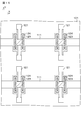
- FIG. 1 is a schematic diagram of a liquid crystal display device according to the first embodiment of the present disclosure.
- FIG. 2A is a schematic cross-sectional view for explaining a basic configuration of a liquid crystal display device.
- FIG. 2B is a schematic circuit diagram for explaining pixels in a liquid crystal display device.
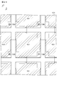
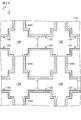
- FIG. 3 is a schematic partial plan view for explaining the plan shape of the light-shielding region in the liquid crystal display device.
- FIG. 4 is a schematic partial plan view for explaining the planar shape of the light guide portion in the liquid crystal display device.
- FIG. 5 is a schematic partial plan view for explaining the planar shape of the polarizing element arranged between the light guide unit and the transparent pixel electrode in the liquid crystal display device.
- FIG. 6 is a schematic partial plan view for explaining the planar shape of the transparent pixel electrode in the liquid crystal display device.
- FIG. 7 is a schematic cross-sectional view when the liquid crystal display device is cut at the portion shown by AA in FIG.
- FIG. 8 is a schematic cross-sectional view when the liquid crystal display device is cut at the portion shown by BB in FIG.
- FIG. 9 is a schematic cross-sectional view when the liquid crystal display device is cut at the portion shown by CC in FIG.
- FIG. 10 is a schematic partial cross-sectional view for explaining the state of light incident on the liquid crystal display device of the reference example.
- FIG. 11 is a schematic partial cross-sectional view for explaining the state of light passing through the light guide portion when the liquid crystal display device of the reference example is in the black display state.
- FIG. 7 is a schematic cross-sectional view when the liquid crystal display device is cut at the portion shown by AA in FIG.
- FIG. 8 is a schematic cross-sectional view when the liquid crystal display device
- FIG. 12 is a schematic partial cross-sectional view for explaining the state of light incident on the liquid crystal display device according to the first embodiment.
- FIG. 13 is a schematic partial plan view of a base material or the like for explaining the manufacturing method of the liquid crystal display device according to the first embodiment.
- FIG. 14 is a schematic partial plan view of a base material or the like for explaining the method of manufacturing the liquid crystal display device according to the first embodiment, following FIG. 13.
- FIG. 15 is a schematic partial plan view of a base material or the like for explaining a method of manufacturing a liquid crystal display device according to the first embodiment, following FIG.
- FIG. 16 is a schematic partial plan view of a base material or the like for explaining a method of manufacturing a liquid crystal display device according to the first embodiment, following FIG. FIG.
- FIG. 17 is a schematic partial plan view of a base material or the like for explaining a method of manufacturing a liquid crystal display device according to the first embodiment
- FIG. 18 is a schematic partial plan view of a base material or the like for explaining a method of manufacturing a liquid crystal display device according to the first embodiment
- FIG. 19 is a schematic partial plan view of a base material or the like for explaining a method of manufacturing a liquid crystal display device according to the first embodiment
- FIG. 20 is a schematic partial plan view of a base material or the like for explaining a method of manufacturing a liquid crystal display device according to the first embodiment, following FIG. 19.
- FIG. 19 is a schematic partial plan view of a base material or the like for explaining a method of manufacturing a liquid crystal display device according to the first embodiment, following FIG. 19.
- FIG. 19 is a schematic partial plan view of a base material or the like for explaining a method of manufacturing a liquid crystal display device according to the first embodiment, following FIG. 19.
- FIG. 19 is a schematic partial plan view of
- FIG. 21 is a schematic partial plan view of a base material or the like for explaining a method of manufacturing a liquid crystal display device according to the first embodiment, following FIG. 20.
- 22A and 22B are schematic partial cross-sectional views of a base material and the like for explaining the process of forming the light guide portion shown in FIG. 21.
- 23A and 23B are schematic partial cross-sectional views of a base material and the like for explaining the process of forming the light guide portion shown in FIG. 21, following FIG. 22B.
- FIG. 24 is a schematic partial plan view of a base material or the like for explaining the method of manufacturing the liquid crystal display device according to the first embodiment, following FIG. 21.
- FIG. 25A, 25B, 25C, 25D, 25E, and 25F are schematic partial cross-sectional views of a base material and the like for explaining the process of forming the polarizing element shown in FIG. 24.
- FIG. 26 is a schematic partial plan view of a base material or the like for explaining a method of manufacturing a liquid crystal display device according to the first embodiment, following FIG. 24.
- FIG. 27 is a schematic partial cross-sectional view of the liquid crystal display device according to the second embodiment of the present disclosure.
- FIG. 28 is a schematic partial plan view of a base material or the like for explaining the planar shape of the light guide portion of the liquid crystal display device according to the second embodiment.
- FIG. 29A and 29B are schematic partial cross-sectional views of a base material and the like for explaining the process of forming the light guide portion shown in FIG. 28.
- 30A and 30B are schematic partial cross-sectional views of a base material and the like for explaining the process of forming the light guide portion shown in FIG. 28, following FIG. 29B.
- FIG. 31 is a schematic partial cross-sectional view of the liquid crystal display device according to the third embodiment of the present disclosure.
- FIG. 32 is a conceptual diagram of a projection type display device.
- 33 is an external view of an interchangeable lens single-lens reflex type digital still camera, the front view thereof is shown in FIG. 33A, and the rear view thereof is shown in FIG. 24B.
- FIG. 34 is an external view of the head-mounted display.
- FIG. 35 is an external view of a see-through head-mounted display.
- the liquid crystal display device according to the present disclosure and the liquid crystal display device used for the electronic device according to the present disclosure may be simply referred to as “the liquid crystal display device of the present disclosure”.
- the electro-optic substrate according to the present disclosure and the electro-optic substrate used in the liquid crystal display device of the present disclosure may be simply referred to as "the electro-optic substrate of the present disclosure”.
- the electro-optical substrate of the present disclosure has a support base material and transparent pixel electrodes arranged in a matrix on the front side of the support base material, and a light guide unit corresponding to each transparent pixel electrode. Is provided on the back surface side of the transparent pixel electrode, and a polarizing element is arranged between the light guide portion and the transparent pixel electrode.
- the light guide includes a translucent material that extends in the normal direction with respect to the supporting substrate and whose wall surface is arranged so as to be in contact with a material having a relatively low refractive index.
- the light guide portion can be configured by providing an opening in the silicon oxide layer and embedding a silicon oxynitride in the opening.
- the material constituting the light guide portion and its surroundings is not particularly limited, and may be appropriately selected depending on the configuration of the electro-optical substrate.
- the light guide portion extends in the normal direction with respect to the supporting base material and includes a light-shielding material arranged so as to surround the wall surface of the translucent material located in the light guide region.
- the light-shielding material can be composed of aluminum (Al), an aluminum alloy such as Al—Cu or Al—Si, and a metal material such as silver (Ag).
- the polarizing element may be configured to consist of a wire grid polarizing element.
- the ratio of the transmittance in the transmission direction of the wire grid polarizing element to the transmittance in the direction orthogonal to the transmission direction is preferably 3 ⁇ 10 3 or more with respect to light having a wavelength of 550 nanometers.
- the wire grid polarizing element can be obtained by, for example, patterning a thin film of aluminum (Al) and appropriately covering it with a protective film.
- the stator can be configured to be electrically floating.
- the stator may be configured to apply a predetermined voltage.
- the stator may be configured such that the same voltage as that applied to the transparent pixel electrode is applied.
- the so-called common potential line (common potential line) and the polarizing element may be made conductive so that the common potential is supplied to the polarizing element.
- the electro-optical substrate of the present disclosure including the above-mentioned various preferable configurations may have a configuration in which yet another polarizing element is arranged on the back surface side of the supporting base material. For example, when the extinguishing ratio by the wire grid polarizing element is insufficient, the required extinguishing ratio can be secured by arranging another polarizing element.
- a substrate made of a transparent material such as glass or quartz can be used as the supporting base material used for the electro-optical substrate.
- the transparent pixel electrode and the counter electrode provided on the facing substrate can be formed by using a transparent conductive material such as indium tin oxide (ITO) or indium zinc oxide (IZO). In some cases, a metal film thin enough to have light transmission can be used.
- the counter electrode functions as a common electrode for each pixel of the liquid crystal display device.
- the thin film transistor constituting the switching element can be configured by forming and processing a semiconductor material layer or the like on the substrate.
- the materials constituting the various wirings and contacts used in the present disclosure are not particularly limited, and are, for example, aluminum (Al), aluminum alloys such as Al—Cu and Al—Si, tungsten (W), and tungsten silicide (WSi). Metallic materials such as tungsten alloys such as x) can be used.
- the insulating layer and the material constituting the insulating film used in the present disclosure are not particularly limited as long as they do not interfere with the implementation of the present disclosure.
- an inorganic material such as silicon oxide or an organic material such as polyimide can be used.
- the liquid crystal display device may be configured to display a monochrome image or may be configured to display a color image.
- pixel values of the liquid crystal display device in addition to U-XGA (1600,1200), HD-TV (1920,1080), Q-XGA (2048,1536), (3840,2160), (7680, Some of the image resolutions, such as 4320), can be exemplified, but are not limited to these values.
- various electronic devices having an image display function can be exemplified in addition to the direct-view type and projection type display devices.
- the first embodiment relates to an electro-optic substrate, a liquid crystal display device, and an electronic device according to the present disclosure.
- FIG. 1 is a schematic diagram for explaining a liquid crystal display device according to the first embodiment of the present disclosure.
- the liquid crystal display device is an active matrix type liquid crystal display device.
- the liquid crystal display device 1 includes various circuits such as pixels PX arranged in a matrix, a horizontal drive circuit 11 for driving the pixels PX, and a vertical drive circuit 12.
- the reference numeral SCL is a scanning line for scanning the pixel PX
- the reference numeral DTL is a signal line for supplying various voltages to the pixel PX.
- M pixels in the horizontal direction and N pixels in the vertical direction, for a total of M ⁇ N are arranged in a matrix.
- the counter electrode shown in FIG. 1 is provided as a common electrode for each liquid crystal cell.
- the horizontal drive circuit 11 and the vertical drive circuit 12 are respectively arranged on one end side of the liquid crystal display device 1, but this is merely an example.
- FIG. 2A is a schematic cross-sectional view for explaining the basic configuration of the liquid crystal display device.
- FIG. 2B is a schematic circuit diagram for explaining pixels in a liquid crystal display device.
- the liquid crystal display device 1 is An electro-optic substrate 100 having a support base material and transparent pixel electrodes arranged in a matrix on the front surface side of the support base material, and Opposing substrate 180 arranged so as to face the electro-optical substrate 100, and The liquid crystal material layer 170 enclosed between the electro-optic substrate 100 and the facing substrate 180, Includes.
- the electro-optic substrate 100 and the facing substrate 180 are sealed by a sealing portion 190.
- the sealing portion 190 is an annular shape surrounding the liquid crystal material layer 170.
- the liquid crystal display device 1 is a transmissive liquid crystal display device.
- the facing substrate 180 is provided with a facing electrode made of a transparent conductive material such as ITO. More specifically, the facing substrate 180 is composed of, for example, a rectangular substrate made of quartz glass, a counter electrode provided on the surface on the liquid crystal material layer 170 side, an alignment film provided on the counter electrode, and the like. There is. Further, a polarizing plate or the like is appropriately attached to the facing substrate 180. For convenience of illustration, the electro-optic substrate 100 and the facing substrate 180 in FIG. 2A are shown in a simplified manner.
- the liquid crystal cell constituting the pixel PX is composed of a transparent pixel electrode provided on the electro-optical substrate 100, a liquid crystal material layer of a portion corresponding to the transparent pixel electrode, and a counter electrode.
- a transparent pixel electrode provided on the electro-optical substrate 100
- a liquid crystal material layer of a portion corresponding to the transparent pixel electrode and a counter electrode.
- positive or negative common potentials V com are alternately applied to the counter electrodes when the liquid crystal display device 1 is driven.
- Each element of the pixel PX, excluding the liquid crystal material layer and the counter electrode, is formed on the electro-optic substrate 100 shown in FIG. 2A.
- one source / drain region of the thin film transistor TR is connected to the signal line DTL, and the other source / drain region is connected to one electrode of the transparent pixel electrode and the capacitance portion CS.
- the pixel voltage supplied from the signal line DTL is applied to the transparent pixel electrode via the thin film transistor TR which is made conductive by the scanning signal of the scanning line SCL. Since the transparent pixel electrode and one electrode of the capacitance portion CS are conducting, the pixel voltage is also applied to one electrode of the capacitance portion CS.
- a common potential V com is applied to the other electrode of the capacitive portion. In this configuration, the voltage of the transparent pixel electrode is held by the capacitance of the liquid crystal cell and the capacitance portion CS even after the thin film transistor TR is brought into a non-conducting state.
- the electro-optical substrate 100 is formed with a light guide portion corresponding to each transparent pixel electrode, and a polarizing element is arranged between the light guide portion and the transparent pixel electrode.
- FIG. 3 is a schematic partial plan view for explaining the plan shape of the light-shielding region in the liquid crystal display device.
- FIG. 4 is a schematic partial plan view for explaining the planar shape of the light guide portion in the liquid crystal display device.
- FIG. 5 is a schematic partial plan view for explaining the planar shape of the polarizing element arranged between the light guide unit and the transparent pixel electrode in the liquid crystal display device.
- FIG. 6 is a schematic partial plan view for explaining the planar shape of the transparent pixel electrode in the liquid crystal display device.
- various wirings and the like are formed on the electro-optical substrate 100.
- a light-shielding region is formed in the liquid crystal display device 1 by these various wirings.
- the hatched portion shows the planar shape of the light-shielding region SHA formed by various wirings and the like.
- the pixel opening region is provided in a region that does not overlap with the light-shielding region SHA.
- FIGS. 3 to 6 Since a large number of components are laminated on the electro-optic substrate 100, the legibility is impaired if all the components are shown on the plan view. Therefore, in FIGS. 3 to 6, only limited elements are displayed. The detailed arrangement relationship of each element will be described in detail with reference to FIGS. 7 to 9.
- a light guide unit LG is formed in a region that does not overlap with the light-shielding region SHA.
- the light guide unit LG includes a translucent material 140 which extends in the normal direction with respect to the supporting base material and whose wall surface is arranged so as to be in contact with a material having a relatively low refractive index.
- the hatched area in FIG. 4 indicates the area where the translucent material 140 is arranged.
- the polarizing element 150 shown in FIG. 5 is arranged above the light guide unit LG shown in FIG.
- the hatched region in FIG. 5 indicates a region in which the polarizing element 150 is arranged.
- the polarizing element 150 is composed of a wire grid polarizing element and is arranged corresponding to each light guide unit LG.
- the transparent pixel electrode 161 shown in FIG. 6 is arranged above the polarizing element 150.
- the hatched region in FIG. 6 indicates a region in which the transparent pixel electrode 161 is arranged.
- the transparent pixel electrode 161, the polarizing element 150, and the light guide unit LG are sequentially laminated. Therefore, the light incident on the transparent pixel electrode 161 via the liquid crystal material layer 170 first passes through the polarizing element 150 and then reaches the light guide unit LG. Therefore, the light reaches the light guide unit LG after passing through the polarizing element 150.
- the display state is not affected.
- FIG. 7 is a schematic cross-sectional view when the liquid crystal display device is cut at the portion shown by AA in FIG.
- FIG. 8 is a schematic cross-sectional view when the liquid crystal display device is cut at the portion shown by BB in FIG.
- FIG. 9 is a schematic cross-sectional view when the liquid crystal display device is cut at the portion shown by CC in FIG.
- the planar shape of each element will be described with reference to FIGS. 13 to 26 for explaining the manufacturing method of the liquid crystal display device 1.
- scanning lines 111 extending in the X direction in the figure (corresponding to SCL in FIG. 1) are placed on the support base material 101. It is formed.
- the hatched portion shows the planar shape of the scanning line 111.
- an insulating film 112 is formed on the entire surface including the scanning line 111, and a semiconductor material layer 121 constituting the thin film transistor TR is formed on the insulating film 112.
- the hatched portion shows the planar shape of the semiconductor material layer 121.
- a gate insulating film 122 is formed on the entire surface including the semiconductor material layer 121, and a gate electrode 124 is formed on the gate insulating film 122.
- the gate insulating film 122 and the insulating film 112 are provided with an opening in which the scanning line 111 is exposed, and a contact 123 between the gate electrode 124 and the scanning line 111 is formed in this portion. ..
- the hatched portion shows the planar shape of the gate electrode 124 and the contact 123.
- an insulating film 125 is formed on the entire surface including the gate electrode 124.
- a wiring layer 130 including a light-shielding film 131 located above the thin film transistor TR is formed on the insulating film 125.
- the wiring layer 130 is configured by laminating a plurality of material layers, and the laminated wiring, electrodes, and the like are separated by an insulating layer.
- various insulating layers constituting the wiring layer 130 may be represented by using reference numerals 130A.
- the light-shielding film 131 is formed of a conductive material having a light-shielding property. As shown in FIG. 9, the insulating film 125 and the gate insulating film 122 are provided with an opening in which the semiconductor material layer 121 is exposed, and a contact 126 is formed in this portion. The light-shielding film 131 conducts with the other source / drain region of the thin film transistor TR via the contact 126. A pixel voltage is applied to the light-shielding film 131 from the signal line via the thin film transistor TR in a conductive state.
- the hatched portion shows the planar shape of the light-shielding film 131 and the contact 126.
- the light-shielding film 131 is formed so as to cover the upper part of the thin film transistor TR.
- an electrode 132 is formed above the light-shielding film 131. As will be described later, a common potential is applied to the electrode 132 from a common potential line, and the electrode 132 functions as an electrode of the capacitance portion CS. In FIG. 17, the hatched portion shows the planar shape of the electrode 132.
- a signal line 134 (corresponding to DTL in FIG. 1) extending in the Y direction in the figure is formed above the electrode 132.
- the wiring layer 130, the insulating film 125, and the gate insulating film 122 are provided with an opening in which the semiconductor material layer 121 is exposed, and a contact 133 is formed in this portion.
- the signal line 134 conducts with one source / drain region of the thin film transistor TR via the contact 133.
- the hatched portion shows the planar shape of the signal line 134 and the contact 133.
- a common potential line 136 extending in the Y direction in the figure is formed above the signal line 134.
- the wiring layer 130 is provided with an opening in which the electrode 132 is exposed, and a contact 135 is formed in this portion.
- the common potential line 136 conducts with the electrode 132 via the contact 135.
- the capacitance portion CS is formed by the electrode 132 and the light-shielding film 131.
- the hatched portion shows the planar shape of the common potential line 136 and the contact 135.
- a relay electrode 138 is formed above the common potential line 136.
- the wiring layer 130 is provided with an opening in which the light-shielding film 131 is exposed, and a contact 137 is formed in this portion.
- the relay electrode 138 conducts with the light-shielding film 131 via the contact 137.
- the hatched portion shows the planar shape of the relay electrode 138 and the contact 137.
- the light-shielding region SHA shown in FIG. 3 is formed by the various wirings and electrodes described above.
- the light guide portion LG shown in FIG. 7 is formed in a region that does not overlap with the light-shielding region SHA.
- the light guide portion LG extends in the normal direction (Z direction in the figure) with respect to the support base material 101, and is a translucent material whose wall surface is arranged so as to be in contact with a material having a relatively low refractive index.
- Contains 140 140.
- the translucent material 140 is formed of silicon oxynitride, and its wall surface is embedded so as to be in contact with a silicon oxide having a relatively low refractive index. Therefore, the light incident on the wall surface of the translucent material 140 exceeding the critical angle is totally reflected.
- the translucent material 140 is formed by engraving the support base material 101 and the wiring layer 130, and is formed so that the end surface is substantially the same as the surface of the relay electrode 138. In FIG. 21, the hatched area indicates the area where
- an insulating film as a surface layer of the wiring layer 130 is formed on the entire surface including the relay electrode 138.
- a transparent pixel electrode 161 formed by dividing a transparent conductive material film into a two-dimensional matrix at a predetermined pitch is formed on the insulating film.
- Reference numeral 139 shown in FIG. 8 indicates the contact between the transparent pixel electrode 161 and the relay electrode 138.
- the pixel voltage held by the capacitance unit CS is supplied to the transparent pixel electrode 161 via the contact 139.
- the hatched portion shows the planar shape of the transparent pixel electrode 161 and the contact 139.
- a flattening film 162 is formed on the entire surface including the transparent pixel electrode 161 and an alignment film 163 is formed on the flattening film 162.
- a polarizing element 150 is arranged between the transparent pixel electrode 161 and the light guide unit LG.
- the polarizing element 150 is composed of a wire grid polarizing element.
- the wire grid modulator is composed of a large number of nano-order metal wires arranged in parallel, transmits an electric field vector perpendicular to the metal wire, and reflects an electric field vector parallel to the metal wire. Therefore, since the wire grid splitter does not absorb light, it also has excellent heat resistance.
- the hatched region indicates a region in which the polarizing element 150 is arranged.
- the ratio of the transmittance of the polarizing element 150 in the transmission direction and the transmittance in the direction orthogonal to the transmission direction is 3 ⁇ 10 3 with respect to light having a wavelength of 550 nanometers. It is preferable to have the above configuration.
- the polarizing element 150 is electrically floating, but the present invention is not limited to this.
- a predetermined voltage may be applied to the polarizing element 150.
- the voltage of the common potential line 136 is applied to the polarizing element 150 by forming necessary contacts as appropriate, or the same voltage as the voltage applied to the transparent pixel electrode 161 by conducting the polarizing element 150 and the relay electrode 138 is applied. It can also be configured to be applied.
- the facing substrate 180 arranged to face the electro-optical substrate 100 is provided on a rectangular base material 181 made of, for example, quartz glass and a surface on the liquid crystal material layer 170 side. It includes an alignment film 183 provided on the counter electrode 182 and the counter electrode 182, and further includes a polarizing element 184 arranged on the base material 181.
- the polarizing element 184 and the polarizing element 150 provided on the electro-optical substrate 100 are arranged in a state in which the polarization axes are orthogonal to each other (cross Nicol).
- the configuration of the polarizing element 184 is not particularly limited, and may be an absorption type polarizing element or a wire grid polarizing element. When heat resistance is required, it is preferable to use the polarizing element 184 as a wire grid polarizing element.
- the liquid crystal material layer 170 is sandwiched between the alignment film 163 of the electro-optical substrate 100 and the alignment film 183 of the facing substrate 180.
- the orientation state of the liquid crystal molecules 171 when there is no electric field is defined by the alignment films 163 and 183.
- the liquid crystal display device 1 is, for example, a vertically oriented (VA) type liquid crystal display device.
- FIG. 10 is a schematic partial cross-sectional view for explaining the state of light incident on the liquid crystal display device of the reference example.
- the liquid crystal display device 9 of the reference example has a configuration in which the polarizing element 150 of the liquid crystal display device 1 is omitted and the polarizing element 950 is arranged on the back surface of the supporting base material 101.
- the extruder 950 and the stator 184 are arranged in a cross-nicol state.
- the light incident on the liquid crystal display device 9 from the light source unit (not shown) is not completely parallel light, but has an angle in the range of, for example, about ⁇ 10 degrees.
- the light incident on the facing substrate 180 passes through the light guide unit LG as it is (light ray A shown in FIG. 10) and when it passes after being totally reflected by the wall surface of the light guide unit LG (light ray B shown in FIG. 10). There is.
- a phase shift called a goose-henshen shift occurs in the light reflected at the interface or the like. Therefore, there is a phase difference between the light ray A that passes through the waveguide without being reflected and the light ray B that is reflected and passed through at the interface or the like.
- FIG. 11 is a schematic partial cross-sectional view for explaining the state of light passing through the light guide unit when the liquid crystal display device of the reference example is in the black display state.
- the liquid crystal material layer 170 does not cause a phase difference with respect to the transmitted light. Since the polarizing element 184 and the polarizing element 950 are in the cross Nicol state, it is desirable that neither the light ray A nor the light ray B passing through the light guide unit LG passes through the polarizing element 950 as a black display state. However, the phase of the light ray B changes with respect to the light ray A due to the phase shift due to reflection. Therefore, a part of the light ray B passes through the polarizing element 950. This is a factor that reduces the contrast of the displayed image.
- phase of the light ray B changes with respect to the light ray A causes a deviation from the originally intended brightness even in the display state of the liquid crystal display device 9.
- Degradation of contrast and deviation from the originally intended brightness are factors that impair the quality of the displayed image.
- the polarizing element 150 is arranged between the transparent pixel electrode 161 and the light guide unit LG.
- FIG. 12 is a schematic partial cross-sectional view for explaining the state of light incident on the liquid crystal display device according to the first embodiment.
- the light incident on the facing substrate 180 passes through the polarizing element 150 and then reaches the light guide unit LG. Therefore, when the liquid crystal display device 1 is in the black display state, neither the light rays A nor the light rays B pass through the polarizing element 150. Therefore, unlike the liquid crystal display device 9, the intended black display state can be obtained. Further, when the liquid crystal display device 1 is in the white display state, both the light rays A and the light rays B pass through the polarizing element 150 and reach the light guide unit LG. Then, the light ray B causes a phase shift, which does not affect the display state. As described above, in the display device 1, the phase shift of the light reflected at the interface or the like does not affect the display state.
- the stray light incident on the transistor can be reduced. Thereby, the leakage of the transistor can be reduced.
- FIGS. 13 to 21, 24 and 26 are schematic plan views, but from the viewpoint of legibility, the display of the insulating layer and the insulating film is omitted in these views.
- the manufacturing method of the liquid crystal display device 1 will be described in detail.
- Step-100 (see FIGS. 8, 9, 13, 14, 14 and 15).
- a scanning line is formed on the supporting substrate.
- a support base material 101 is prepared, and scanning lines 111 are formed on the support base material 101 by a well-known film forming method or patterning method (see FIG. 13).
- the scanning line 111 is made of a metal material such as tungsten (W) or Al—Cu. The same applies to other wirings and electrodes described later.
- a thin film transistor TR is formed above the scanning line 111.
- An insulating film 112 made of, for example, a silicon oxide is formed on the entire surface including the scanning line 111, and a semiconductor material layer 121 constituting the thin film transistor TR is formed on the insulating film 112 by a well-known film forming method or patterning method (FIG. 14). reference).
- a gate insulating film 122 made of, for example, a silicon oxide is formed on the entire surface including the semiconductor material layer 121.
- an opening is provided in the gate insulating film 122 and the insulating film 112 in the portion corresponding to the contact 123.
- a conductive material is embedded in the opening to form the contact 123, and then the gate electrode 124 is formed by a well-known film forming method or patterning method (see FIG. 15).
- the thin film transistor TR is formed above the scanning line 111.
- an insulating film 125 made of, for example, a silicon oxide is formed on the entire surface including the gate electrode 124.
- Step-110 (see FIGS. 8, 9, 16 and 17) After that, the light-shielding film 131 is formed above the thin film transistor TR. First, an opening is provided in the insulating film 125 or the like corresponding to the contact 126 to expose the semiconductor material layer 121. Next, a conductive material is embedded in the opening to form the contact 126, and then the light-shielding film 131 is formed by a well-known film forming method or patterning method (see FIG. 16). The light-shielding film 131 is connected to the semiconductor material layer 121 via the contact 126 (see FIG. 9).
- the electrode 132 constituting the capacitance portion CS is formed above the light-shielding film 131.
- An insulating layer made of, for example, a silicon oxide is formed on the entire surface including the light-shielding film 131, and then an electrode 132 is formed on the insulating layer by a well-known film forming method or patterning method (see FIG. 17).
- a signal line 134 is formed above the electrode 132.
- an insulating layer made of, for example, a silicon oxide on the entire surface including the electrode 132, an opening is provided in a portion corresponding to the contact 133 to expose the semiconductor material layer 121.
- a conductive material is embedded in the opening to form the contact 133, and then the signal line 134 is formed by a well-known film forming method or patterning method (see FIG. 18).
- the signal line 134 is connected to the semiconductor material layer 121 via the contact 133 (see FIG. 9).
- a common potential line 136 is formed above the signal line 134.
- an insulating layer made of, for example, a silicon oxide on the entire surface including the signal line 134, an opening is provided in a portion corresponding to the contact 135 to expose the electrode 132.
- a conductive material is embedded in the opening to form the contact 135, and then the common potential line 136 is formed by a well-known film forming method or patterning method (see FIG. 19).
- the common potential line 136 is connected to the electrode 132 via the contact 135 (see FIG. 8).
- Step-130 (see FIGS. 8, 9, and 20)
- the relay electrode 138 is formed above the common potential line 136.
- an insulating layer made of, for example, a silicon oxide on the entire surface including the common potential line 136
- an opening is provided in a portion corresponding to the contact 137 to expose the light-shielding film 131.
- a conductive material is embedded in the opening to form the contact 137, and then the relay electrode 138 is formed by a well-known film forming method or patterning method (see FIG. 20).
- the relay electrode 138 is connected to the light-shielding film 131 via the contact 137 (see FIG. 8).
- Step-140 (see FIGS. 7, 21, 22A, 22B, 23A and 23B).
- the light guide unit LG is formed.
- An insulating layer made of, for example, a silicon oxide is formed on the entire surface including the relay electrode 138, and then flattened so that the relay electrode 138 is exposed (see FIG. 22A).
- an opening OP is provided in the portion to be embedded with the translucent material 140 shown in FIG. 21 (see FIG. 22B).
- a silicon oxynitride is formed on the entire surface of the translucent material 140 to embed the inside of the opening OP (see FIG. 23A). Then, for example, flattening is performed so that the relay electrode 138 is exposed. After that, an insulating film 130A made of, for example, a silicon oxide is formed on the entire surface (see FIG. 23B). By the above steps, the light guide unit LG can be obtained.
- Step-150 (see FIGS. 7, 24, 25A, 25B, 25C, 25D, 25E and 25F).
- the polarizing element 150 is formed above the light guide unit LG.
- a metal film 151A made of, for example, aluminum (Al) is formed on the insulating film 130A (see FIG. 25A).
- a resist is patterned on the resist to form a mask 152 (see FIG. 25B).
- the metal film 151A is patterned by using, for example, a dry etching method, and a large number of nano-order metal wires 151 are arranged in parallel in the region indicated by reference numeral 150 in FIG. 24 (see FIG. 25C).
- the mask 152 is removed (FIG. 25D), and then a protective film 153 made of, for example, a silicon oxide is formed (FIG. 25E).
- a protective film 153 made of, for example, a silicon oxide is formed (FIG. 25E).
- the polarizing element 150 can be formed.
- the extinction ratio of the wire grid polarizing element increases as the refractive index of the substance between the wire grids decreases. Therefore, for example, as shown in FIG. 25F, the protective film 153 may be formed so that a void 154 is formed between the metal wire 151 and the metal wire 151.
- the transparent pixel electrode 161 is formed above the polarizing element 150.
- an opening is provided in a portion corresponding to the contact 139 to expose the relay electrode 138.
- a conductive material is embedded in the opening to form the contact 138, and then the transparent pixel electrode 161 is formed by a well-known film forming method or patterning method (see FIG. 26).
- the transparent pixel electrode 161 is connected to the light-shielding film 131 constituting the electrode of the capacitance portion CS via the contact 139, the relay electrode 138, and the contact 137.
- a flattening film 162 made of, for example, a silicon oxide is formed on the entire surface including the transparent pixel electrode 161 and then an alignment film 163 is further formed.
- the electro-optical substrate 100 used in the liquid crystal display device 1 can be obtained.
- a facing substrate 180 having a rectangular base material 181 made of, for example, quartz glass, a counter electrode 182 provided on one surface of the base material 181 and an alignment film 183 provided on the facing electrode 182 is prepared. do. Then, the electro-optic substrate 100 and the facing substrate 180 are opposed to each other with the liquid crystal material layer 170 sandwiched therein, and the periphery is sealed. After that, the liquid crystal display device 1 can be obtained by arranging the polarizing element 184 on the other surface of the base material 181.
- the second embodiment also relates to an electro-optic substrate, a liquid crystal display device, and an electronic device according to the present disclosure.
- FIG. 27 is a schematic partial cross-sectional view of the liquid crystal display device according to the second embodiment of the present disclosure, and is a drawing corresponding to FIG. 7 referred to in the first embodiment.
- the liquid crystal display device 1 may be read as the liquid crystal display device 2 in FIG.
- the light guide portion extends in the normal direction with respect to the supporting base material and is arranged so as to surround the wall surface of the translucent material located in the light guide region. It contained a light-shielding material.
- the light guide portion extends in the normal direction with respect to the support base material and has a wall surface of a translucent material located in the light guide region. The difference is that it contains a light-shielding material arranged so as to surround it.
- FIG. 28 is a schematic partial plan view of a base material or the like for explaining the planar shape of the light guide portion of the liquid crystal display device according to the second embodiment.
- the light guide portion LG extends in the normal direction with respect to the support base material 101 and surrounds the wall surface of the translucent material located in the light guide region.
- a light-shielding material 240 located in.
- the light-shielding material 240 is made of a metal material such as aluminum (Al) or silver (Ag).
- Al aluminum
- Ag silver
- FIG. 28 in the region surrounded by the light-shielding material 240, the same material as the material constituting the insulating layer used for the wiring layer 130, for example, silicon oxide is embedded.
- the light incident on the facing substrate 180 reaches the light guide unit LG after passing through the polarizing element 150.
- the light reflected by the light-shielding material 240 of the light guide unit LG causes a phase shift, which affects the display state as described with reference to FIG. 12 in the first embodiment. There is no such thing.
- the thin film transistor TR is located outside the region surrounded by the light-shielding material 240. Therefore, the stray light incident on the thin film transistor TR can be reduced. Thereby, the leakage of the thin film transistor TR can be reduced.
- 29 and 30 are various drawings for explaining the manufacturing method of the liquid crystal display device 2.
- Step-210 (see FIGS. 28, 29A, 29B, 30A and 30B).
- the light guide unit LG is formed.
- An insulating layer made of, for example, a silicon oxide is formed on the entire surface including the relay electrode 138, and then flattened so that the relay electrode 138 is exposed, for example.
- an opening OP is provided so that the wall surface forming the light-shielding material 240 shown in FIG. 28 is exposed (see FIG. 29A).
- a light-shielding material 240 is formed on the wall surface of the opening OP (see FIG. 29B).
- an insulating film 130A made of, for example, a silicon oxide is formed on the entire surface to fill the inside of the opening (see FIG. 30A). Then, for example, flattening is performed so that the relay electrode 138 is not exposed (see FIG. 30B). By the above steps, the light guide unit LG can be obtained.
- a third embodiment also relates to an electro-optic substrate, a liquid crystal display device, and an electronic device according to the present disclosure.
- FIG. 31 is a schematic partial cross-sectional view of the liquid crystal display device according to the third embodiment of the present disclosure, and is a drawing corresponding to FIG. 7 referred to in the first embodiment.
- the liquid crystal display device 1 may be read as the liquid crystal display device 3 in FIG.
- the polarizing element of the electro-optical substrate 100 is arranged between the transparent pixel electrode and the light guide unit.
- the liquid crystal display device 3 according to the third embodiment is different in that yet another polarizing element is arranged on the back surface side of the supporting base material of the electro-optical substrate. Except for the above points, the configuration is the same as that of the liquid crystal display device 1.
- the liquid crystal display device 2 described in the second embodiment may also have a configuration in which another polarizing element 350 is arranged on the back surface side of the support base material 101 of the electro-optical substrate 200.
- the configuration of the polarizing element 350 is not particularly limited, and may be an absorption type polarizing element or a wire grid polarizing element. When heat resistance is required, it is preferable to use the polarizing element 350 as a wire grid polarizing element.
- the liquid crystal display device is a display unit (display device) of an electronic device in all fields for displaying a video signal input to an electronic device or a video signal generated in the electronic device as an image or a video.
- a display unit such as a television set, a digital still camera, a notebook personal computer, a portable terminal device such as a mobile phone, a video camera, and a head mount display (head-mounted display).
- the liquid crystal display device of the present disclosure also includes a modular one having a sealed configuration.
- a display module formed by attaching a facing portion such as a transparent glass material to a pixel array portion is applicable.
- the display module may be provided with a circuit unit for inputting / outputting a signal or the like from the outside to the pixel array unit, a flexible printed circuit (FPC), or the like.
- FPC flexible printed circuit
- FIG. 32 is a conceptual diagram of a projection type display device using the liquid crystal display device of the present disclosure.
- the projection type display device includes a light source unit 400, an illumination optical system 410, a liquid crystal display device 1, an image control circuit 420 for driving the liquid crystal display device, a projection optical system 430, a screen 440, and the like.
- the light source unit 400 can be composed of, for example, various lamps such as xenon lamps and semiconductor light emitting elements such as light emitting diodes.
- the illumination optical system 410 is used to guide the light from the light source unit 400 to the liquid crystal display device 1, and is composed of optical elements such as a prism and a dichroic mirror.
- the liquid crystal display device 1 acts as a light bulb, and an image is projected on the screen 440 via the projection optical system 430.
- the interchangeable-lens single-lens reflex type digital still camera has, for example, an interchangeable photographing lens unit (interchangeable lens) 512 on the front right side of the camera body (camera body) 511, and is held by the photographer on the front left side. It has a grip portion 513 for the purpose.
- interchangeable photographing lens unit interchangeable lens
- a monitor 514 is provided in the center of the back of the camera body 511.
- a viewfinder (eyepiece window) 515 is provided on the upper part of the monitor 514. By looking into the viewfinder 515, the photographer can visually recognize the optical image of the subject guided from the photographing lens unit 512 and determine the composition.
- the liquid crystal display device of the present disclosure can be used as the viewfinder 515. That is, the interchangeable lens type single-lens reflex type digital still camera according to this example is manufactured by using the liquid crystal display device of the present disclosure as its viewfinder 515.
- FIG. 34 is an external view of the head-mounted display.
- the head-mounted display has, for example, ear hooks 612 for being worn on the user's head on both sides of the eyeglass-shaped display unit 611.
- the liquid crystal display device of the present disclosure can be used as the display unit 611. That is, the head-mounted display according to this example is manufactured by using the liquid crystal display device of the present disclosure as the display unit 611.
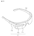
- FIG. 35 is an external view of a see-through head-mounted display.
- the see-through head-mounted display 711 is composed of a main body portion 712, an arm 713, and a lens barrel 714.
- the main body 712 is connected to the arm 713 and the glasses 700. Specifically, the end portion of the main body portion 712 in the long side direction is connected to the arm 713, and one side of the side surface of the main body portion 712 is connected to the eyeglasses 700 via a connecting member.
- the main body portion 712 may be directly attached to the head of the human body.
- the main body 712 incorporates a control board for controlling the operation of the see-through head-mounted display 711 and a display unit.
- the arm 713 connects the main body 712 and the lens barrel 714, and supports the lens barrel 714. Specifically, the arm 713 is coupled to the end of the main body 712 and the end of the lens barrel 714, respectively, to fix the lens barrel 714. Further, the arm 713 has a built-in signal line for communicating data related to an image provided from the main body portion 712 to the lens barrel 714.
- the lens barrel 714 projects the image light provided from the main body 712 via the arm 713 toward the eyes of the user who wears the see-through head-mounted display 711 through the eyepiece.
- the liquid crystal display device of the present disclosure can be used for the display unit of the main body unit 712.
- A1 It has a support base material and transparent pixel electrodes arranged in a matrix on the front side of the support base material.
- a light guide unit corresponding to each transparent pixel electrode is provided on the back surface side of the transparent pixel electrode.
- a polarizing element is arranged between the light guide unit and the transparent pixel electrode.
- Electro-optic substrate [A2] The light guide extends in the normal direction with respect to the supporting substrate and contains a translucent material whose wall surface is arranged so as to be in contact with a material having a relatively low refractive index.
- the electro-optic substrate according to the above [A1].
- the light guide extends in the normal direction with respect to the supporting substrate and includes a light shielding material arranged so as to surround the wall surface of the translucent material located in the light guide region.
- the electro-optic substrate according to the above [A1].
- the light-shielding material consists of a metallic material, The electro-optic substrate according to the above [A3].
- the modulator consists of a wire grid modulator, The electro-optical substrate according to any one of the above [A1] to [A4].
- the ratio of the transmittance of the transducer in the transmission direction to the transmittance in the direction orthogonal to the transmission direction is 3 ⁇ 10 3 or more with respect to light having a wavelength of 550 nanometers.
- the transducer is electrically floating, The electro-optic substrate according to the above [A5].
- a predetermined voltage is applied to the splitter, The electro-optic substrate according to the above [A5].
- A9] The same voltage as that applied to the transparent pixel electrode is applied to the polarizing element.
- Yet another substituent is placed on the back side of the supporting substrate, The electro-optical substrate according to any one of the above [A1] to [A9].
- An electro-optic substrate having a support base material and transparent pixel electrodes arranged in a matrix on the front side of the support base material, Opposing boards arranged to face the electro-optic board, A liquid crystal material layer enclosed between the electro-optic substrate and the facing substrate, Includes A light guide unit corresponding to each transparent pixel electrode is provided on the back surface side of the transparent pixel electrode. A polarizing element is arranged between the light guide unit and the transparent pixel electrode. Liquid crystal display device. [B2] The light guide extends in the normal direction with respect to the supporting substrate and contains a translucent material whose wall surface is arranged so as to be in contact with a material having a relatively low refractive index. The liquid crystal display device according to the above [B1].
- the light guide extends in the normal direction with respect to the supporting substrate and includes a light shielding material arranged so as to surround the wall surface of the translucent material located in the light guide region.
- the light-shielding material consists of a metallic material, The liquid crystal display device according to the above [B3].
- the modulator consists of a wire grid modulator, The liquid crystal display device according to any one of the above [B1] to [B4].
- the ratio of the transmittance of the transducer in the transmission direction to the transmittance in the direction orthogonal to the transmission direction is 3 ⁇ 10 3 or more with respect to light having a wavelength of 550 nanometers.
- the liquid crystal display device according to the above [B5].
- the transducer is electrically floating, The liquid crystal display device according to the above [B5].
- a predetermined voltage is applied to the splitter, The liquid crystal display device according to the above [B5].
- B9 The same voltage as that applied to the transparent pixel electrode is applied to the polarizing element.
- the liquid crystal display device according to the above [B8].
- Yet another substituent is placed on the back side of the supporting substrate, The liquid crystal display device according to any one of the above [B1] to [B9].
- An electro-optic substrate having a support base material and transparent pixel electrodes arranged in a matrix on the front side of the support base material, Opposing boards arranged to face the electro-optic board, A liquid crystal material layer enclosed between the electro-optic substrate and the facing substrate, Includes A light guide unit corresponding to each transparent pixel electrode is provided on the back surface side of the transparent pixel electrode. A polarizing element is arranged between the light guide unit and the transparent pixel electrode. An electronic device equipped with a liquid crystal display device. [C2] The light guide extends in the normal direction with respect to the supporting substrate and contains a translucent material whose wall surface is arranged so as to be in contact with a material having a relatively low refractive index.
- the electronic device according to the above [C1].
- the light guide extends in the normal direction with respect to the supporting substrate and includes a light shielding material arranged so as to surround the wall surface of the translucent material located in the light guide region.
- the electronic device according to the above [C1].
- the light-shielding material consists of a metallic material, The electronic device according to the above [C3].
- the modulator consists of a wire grid modulator, The electronic device according to any one of the above [C1] to [C4].
- the ratio of the transmittance of the transducer in the transmission direction to the transmittance in the direction orthogonal to the transmission direction is 3 ⁇ 10 3 or more with respect to light having a wavelength of 550 nanometers.
- the transducer is electrically floating, The electronic device according to the above [C5].
- a predetermined voltage is applied to the splitter, The electronic device according to the above [C5].
- [C9] The same voltage as that applied to the transparent pixel electrode is applied to the polarizing element.
- [C10] Yet another substituent is placed on the back side of the supporting substrate, The electronic device according to any one of the above [C1] to [C9].
- Electro-optical substrate 101 ... Support substrate, 111 ... Scanning line, 112 ... insulating film, 121 ... semiconductor material layer, 122 ... gate insulating film, 123 ... contact, 124 ... gate electrode, 125 ... insulating film, 126 ... Contact, 130 ... wiring layer, 130A ... various insulating layers constituting the wiring layer, 131 ... light-shielding film, 132 ... electrode 133 ... contact, 134 ... signal line, 135 ... Contact, 136 ... Common potential line, 137 ... Contact, 138 ... Relay electrode, 139 ... Contact, 150 ...
- Polarizer 151A ... Metal film, 151 ... Wire grid, 152 ... Mask, 153 ... Protective film, 154 ... Void, 161 ... Transparent pixel electrode, 162 ... Flattening film, 163 ... Alignment film, 170 ... Liquid crystal Material layer, 171 ... liquid crystal molecule, 180 ... opposed substrate, 181 ... base material, 182 ... opposed electrode, 183 ... alignment film, 184 ... polarizing element, SHA ... shading Region, LG ... light guide unit, SCL ... scanning line, DTL ... signal line, PX ... pixel, TR ... thin film, CS ... capacitive part, 200 ... electro-optical substrate , 240 ...
- Light-shielding material 300 ... Electro-optical substrate, 350 ... Polarizer, 950 ... Polarizer, 400 ...
- Light source unit 410 ... Illumination optical system, 420 ... Image control circuit, 430 ... Projection optical system, 440 ... Screen, 511 ... Camera body, 512 ... Shooting lens unit, 513 ... Grip, 514 ... Monitor, 515 ... -Viewfinder, 611 ... optics-shaped display, 612 ... ear hook, 700 ... glasses, 711 ... see-through head mount display, 712 ... main body, 713 ... arm, 714 ... lens barrel
Abstract
[Problem] To provide an electrooptical substrate, a liquid crystal display device, and an electronic apparatus in which the phase shift of light reflected at an interface or the like does not influence a display state. [Solution] This liquid crystal display device includes an electrooptical substrate having a support base material and transparent pixel electrodes disposed in a matrix form on the front surface side of the support base material, an opposite substrate disposed so as to be opposite to the electrooptical substrate, and a liquid crystal material layer sealed between the electrooptical substrate and the opposite substrate. A light guiding part corresponding to each of the transparent pixel electrodes is provided on the back surface side of the transparent pixel electrode, and a polarizer is disposed between the light guiding part and the transparent pixel electrode.
Description
本開示は、電気光学基板、液晶表示装置および電子機器に関する。
This disclosure relates to an electro-optical substrate, a liquid crystal display device, and an electronic device.
マトリクス状に配置された透明画素電極が配置された電気光学基板と、電気光学基板と対向するように配置された対向基板と、電気光学基板と対向基板との間に封入された液晶材料層とを含んでいる液晶表示装置が知られている。液晶表示装置は、画素を光シャッター(ライト・バルブ)として動作させることによって画像を表示する。近年、液晶表示装置にあっては、高精細化と共に高輝度化も要求されている。
An electro-optic substrate in which transparent pixel electrodes arranged in a matrix are arranged, a facing substrate arranged so as to face the electro-optical substrate, and a liquid crystal material layer enclosed between the electro-optic substrate and the facing substrate. A liquid crystal display device containing the above is known. The liquid crystal display device displays an image by operating the pixel as an optical shutter (light bulb). In recent years, liquid crystal display devices are required to have high definition as well as high brightness.
アクティブマトリクス方式の液晶表示装置にあっては、スイッチング素子(例えばトランジスタ)を介して透明画素電極に電圧を印加した後、トランジスタが非導通状態とされる。そして、画素容量が電圧を保持することによって表示を行う。従って、非導通状態であるべきトランジスタにリーク電流が流れると保持電圧が変化し、結果として表示品質が劣化する。また、トランジスタに光が入射するとキャリアが誘起されリーク電流は増加する。
In the active matrix type liquid crystal display device, after applying a voltage to the transparent pixel electrode via a switching element (for example, a transistor), the transistor is put into a non-conducting state. Then, the pixel capacitance holds the voltage to display the voltage. Therefore, when a leak current flows through a transistor that should be in a non-conducting state, the holding voltage changes, and as a result, the display quality deteriorates. Further, when light is incident on the transistor, carriers are induced and the leakage current increases.
トランジスタに入射する方向に進む光の進行方向を変えて、表示に寄与する光として利用することができれば、表示装置の高輝度化を図り且つトランジスタのリーク電流を低減することができる。例えば、特許文献1には、開口領域に導波路構造を設けることによって、出射する光量の増加を図ると共にトランジスタへの光入射を抑制するといった技術が開示されている。
If the traveling direction of the light traveling in the direction incident on the transistor can be changed and used as the light contributing to the display, the brightness of the display device can be increased and the leakage current of the transistor can be reduced. For example, Patent Document 1 discloses a technique of increasing the amount of emitted light and suppressing light incident on a transistor by providing a waveguide structure in an opening region.
界面等で反射する光にはグース・ヘンシェンシフトと呼ばれる位相シフトが生ずる。このため、導波路内を反射することなく通過する光と界面等で反射して通過する光との間には、位相差が生ずる。これによって、黒表示状態であるにもかかわらず導波路から出射する光の一部が出射側の偏光子を透過したり、あるいは又、白表示状態において導波路から出射する光の一部が出射側の偏光子を透過しないといったことが生じ得る。これらは、表示される画像のコントラストの低下要因となる。
A phase shift called goose-henshen shift occurs in the light reflected at the interface. Therefore, a phase difference occurs between the light that passes through the waveguide without being reflected and the light that is reflected at the interface or the like and passes through. As a result, a part of the light emitted from the waveguide in the black display state passes through the polarizing element on the emitting side, or a part of the light emitted from the waveguide in the white display state is emitted. It may happen that it does not pass through the polarizing element on the side. These are factors that reduce the contrast of the displayed image.
従って、本開示の目的は、界面等で反射する光の位相シフトが表示状態に影響を与えることがない電気光学基板、液晶表示装置および電子機器を提供することにある。
Therefore, an object of the present disclosure is to provide an electro-optical substrate, a liquid crystal display device, and an electronic device in which the phase shift of light reflected at an interface or the like does not affect the display state.
上記の目的を達成するための本開示に係る電気光学基板は、
支持基材と支持基材の前面側にマトリクス状に配置された透明画素電極とを有しており、
各透明画素電極に対応した導光部が透明画素電極の裏面側に設けられており、
導光部と透明画素電極との間には偏光子が配置されている、
電気光学基板である。 The electro-optic substrate according to the present disclosure for achieving the above object is
It has a support base material and transparent pixel electrodes arranged in a matrix on the front side of the support base material.
A light guide unit corresponding to each transparent pixel electrode is provided on the back surface side of the transparent pixel electrode.
A polarizing element is arranged between the light guide unit and the transparent pixel electrode.
It is an electro-optic substrate.
上記の目的を達成するための本開示に係る液晶表示装置は、
支持基材と支持基材の前面側にマトリクス状に配置された透明画素電極とを有する電気光学基板と、
電気光学基板と対向するように配置された対向基板と、
電気光学基板と対向基板との間に封入された液晶材料層と、
を含んでおり、
各透明画素電極に対応した導光部が透明画素電極の裏面側に設けられており、
導光部と透明画素電極との間には偏光子が配置されている、
液晶表示装置である。 The liquid crystal display device according to the present disclosure for achieving the above object is
An electro-optic substrate having a support base material and transparent pixel electrodes arranged in a matrix on the front side of the support base material,
Opposing boards arranged to face the electro-optic board,
A liquid crystal material layer enclosed between the electro-optic substrate and the facing substrate,
Includes
A light guide unit corresponding to each transparent pixel electrode is provided on the back surface side of the transparent pixel electrode.
A polarizing element is arranged between the light guide unit and the transparent pixel electrode.
It is a liquid crystal display device.
上記の目的を達成するための本開示に係る電子機器は、
支持基材と支持基材の前面側にマトリクス状に配置された透明画素電極とを有する電気光学基板と、
電気光学基板と対向するように配置された対向基板と、
電気光学基板と対向基板との間に封入された液晶材料層と、
を含んでおり、
各透明画素電極に対応した導光部が透明画素電極の裏面側に設けられており、
導光部と透明画素電極との間には偏光子が配置されている、
液晶表示装置を備えた電子機器である。 The electronic devices pertaining to this disclosure to achieve the above objectives are:
An electro-optic substrate having a support base material and transparent pixel electrodes arranged in a matrix on the front side of the support base material,
Opposing boards arranged to face the electro-optic board,
A liquid crystal material layer enclosed between the electro-optic substrate and the facing substrate,
Includes
A light guide unit corresponding to each transparent pixel electrode is provided on the back surface side of the transparent pixel electrode.
A polarizing element is arranged between the light guide unit and the transparent pixel electrode.
It is an electronic device equipped with a liquid crystal display device.
以下、図面を参照して、実施形態に基づいて本開示を説明する。本開示は実施形態に限定されるものではなく、実施形態における種々の数値や材料は例示である。以下の説明において、同一要素または同一機能を有する要素には同一符号を用いることとし、重複する説明は省略する。尚、説明は、以下の順序で行う。
1.本開示に係る、電気光学基板、液晶表示装置および電子機器、全般に関する説明
2.第1の実施形態
3.第2の実施形態
4.第3の実施形態
5.電子機器の説明
6.その他 Hereinafter, the present disclosure will be described with reference to the drawings. The present disclosure is not limited to embodiments, and various numerical values and materials in the embodiments are examples. In the following description, the same code will be used for the same element or the element having the same function, and duplicate description will be omitted. The explanation will be given in the following order.
1. 1. Description of the electro-optic substrate, liquid crystal display device, electronic device, and general related to the present disclosure.First embodiment 3. Second embodiment 4. Third embodiment 5. Explanation of electronic devices 6. others
1.本開示に係る、電気光学基板、液晶表示装置および電子機器、全般に関する説明
2.第1の実施形態
3.第2の実施形態
4.第3の実施形態
5.電子機器の説明
6.その他 Hereinafter, the present disclosure will be described with reference to the drawings. The present disclosure is not limited to embodiments, and various numerical values and materials in the embodiments are examples. In the following description, the same code will be used for the same element or the element having the same function, and duplicate description will be omitted. The explanation will be given in the following order.
1. 1. Description of the electro-optic substrate, liquid crystal display device, electronic device, and general related to the present disclosure.
[本開示に係る、電気光学基板、液晶表示装置および電子機器、全般に関する説明]
以下の説明において、本開示に係る液晶表示装置および本開示に係る電子機器に用いられる液晶表示装置を、単に、「本開示の液晶表示装置」と呼ぶ場合がある。また、本開示に係る電気光学基板および本開示の液晶表示装置に用いられる電気光学基板を、単に、「本開示の電気光学基板」と呼ぶ場合がある。
[Explanation of Electro-Optical Substrates, Liquid Crystal Display Devices and Electronic Devices Related to the Disclosure]
In the following description, the liquid crystal display device according to the present disclosure and the liquid crystal display device used for the electronic device according to the present disclosure may be simply referred to as "the liquid crystal display device of the present disclosure". Further, the electro-optic substrate according to the present disclosure and the electro-optic substrate used in the liquid crystal display device of the present disclosure may be simply referred to as "the electro-optic substrate of the present disclosure".
上述したように、本開示の電気光学基板は、支持基材と支持基材の前面側にマトリクス状に配置された透明画素電極とを有しており、各透明画素電極に対応した導光部が透明画素電極の裏面側に設けられており、導光部と透明画素電極との間には偏光子が配置されている。
As described above, the electro-optical substrate of the present disclosure has a support base material and transparent pixel electrodes arranged in a matrix on the front side of the support base material, and a light guide unit corresponding to each transparent pixel electrode. Is provided on the back surface side of the transparent pixel electrode, and a polarizing element is arranged between the light guide portion and the transparent pixel electrode.
この場合において、導光部は、支持基材に対して法線方向に延在すると共に、その壁面が相対的に屈折率の低い材料と接するように配置されている透光性材料を含んでいる構成とすることができる。例えば、シリコン酸化物層に開口を設け、その中にシリコン酸窒化物を埋め込むことによって導光部を構成することができる。導光部やその周辺を構成する材料は特に限定するものではなく、電気光学基板の構成に応じて、適宜選択すればよい。
In this case, the light guide includes a translucent material that extends in the normal direction with respect to the supporting substrate and whose wall surface is arranged so as to be in contact with a material having a relatively low refractive index. Can be configured as For example, the light guide portion can be configured by providing an opening in the silicon oxide layer and embedding a silicon oxynitride in the opening. The material constituting the light guide portion and its surroundings is not particularly limited, and may be appropriately selected depending on the configuration of the electro-optical substrate.
あるいは又、導光部は、支持基材に対して法線方向に延在すると共に、導光領域に位置する透光性材料の壁面を囲むように配置された遮光性材料を含んでいる構成とすることができる。この場合において、遮光性材料は、アルミニウム(Al)、Al-CuやAl-Si等のアルミニウム合金、銀(Ag)等の金属材料から成る構成とすることができる。
Alternatively, the light guide portion extends in the normal direction with respect to the supporting base material and includes a light-shielding material arranged so as to surround the wall surface of the translucent material located in the light guide region. Can be. In this case, the light-shielding material can be composed of aluminum (Al), an aluminum alloy such as Al—Cu or Al—Si, and a metal material such as silver (Ag).
上述した各種の好ましい構成を含む本開示の電気光学基板において、偏光子はワイヤーグリッド偏光子から成る構成とすることができる。この場合において、ワイヤーグリッド偏光子の透過方向の透過率と透過方向と直交する方向の透過率の比は、波長550ナノメートルの光に対して3×10³以上であることが好ましい。ワイヤーグリッド偏光子は、例えばアルミニウム(Al)の薄膜にパターニングを施し、適宜保護膜で覆うなどといった工程によって得ることができる。
In the electro-optic substrate of the present disclosure including the various preferable configurations described above, the polarizing element may be configured to consist of a wire grid polarizing element. In this case, the ratio of the transmittance in the transmission direction of the wire grid polarizing element to the transmittance in the direction orthogonal to the transmission direction is preferably 3 × 10 3 or more with respect to light having a wavelength of 550 nanometers. The wire grid polarizing element can be obtained by, for example, patterning a thin film of aluminum (Al) and appropriately covering it with a protective film.
この場合において、偏光子は電気的にフローティングとされる構成とすることができる。あるいは又、偏光子には所定の電圧が印加される構成とすることができる。例えば、偏光子には透明画素電極に印加される電圧と同じ電圧が印加されるといった構成とすることができる。あるいは又、所謂共通電位線(コモン電位線)と偏光子とを導通させ、共通電位が偏光子に供給される構成とすることもできる。
In this case, the stator can be configured to be electrically floating. Alternatively, the stator may be configured to apply a predetermined voltage. For example, the stator may be configured such that the same voltage as that applied to the transparent pixel electrode is applied. Alternatively, the so-called common potential line (common potential line) and the polarizing element may be made conductive so that the common potential is supplied to the polarizing element.
上述した各種の好ましい構成を含む本開示の電気光学基板にあっては、支持基材の背面側に更に別の偏光子が配置されている構成とすることができる。例えば、ワイヤーグリッド偏光子による消光比が不足している場合に、更に別の偏光子を配置することによって、必要とされる消光比を確保することができる。
The electro-optical substrate of the present disclosure including the above-mentioned various preferable configurations may have a configuration in which yet another polarizing element is arranged on the back surface side of the supporting base material. For example, when the extinguishing ratio by the wire grid polarizing element is insufficient, the required extinguishing ratio can be secured by arranging another polarizing element.
電気光学基板に用いられる支持基材として、ガラスや石英などの透明材料から成る基板を用いることができる。対向基板に用いられる基材についても同様である。透明画素電極や対向基板に設けられる対向電極は、インジウムスズ酸化物(ITO)やインジウム亜鉛酸化物(IZO)などの透明導電材料を用いて形成することができる。尚、場合によっては、光透過性を有するほどに薄膜化した金属膜を用いることもできる。対向電極は、液晶表示装置の各画素に対する共通電極として機能する。
As the supporting base material used for the electro-optical substrate, a substrate made of a transparent material such as glass or quartz can be used. The same applies to the base material used for the facing substrate. The transparent pixel electrode and the counter electrode provided on the facing substrate can be formed by using a transparent conductive material such as indium tin oxide (ITO) or indium zinc oxide (IZO). In some cases, a metal film thin enough to have light transmission can be used. The counter electrode functions as a common electrode for each pixel of the liquid crystal display device.
本開示の電気光学基板において、スイッチング素子を構成する薄膜トランジスタは、基材上に半導体材料層等を形成し加工することによって構成することができる。
In the electro-optical substrate of the present disclosure, the thin film transistor constituting the switching element can be configured by forming and processing a semiconductor material layer or the like on the substrate.
本開示に用いられる各種の配線やコンタクトを構成する材料は特に限定するものではなく、例えば、アルミニウム(Al)、Al-CuやAl-Si等のアルミニウム合金、タングステン(W)、タングステンシリサイド(WSix)などのタングステン合金といった金属材料を用いることができる。
The materials constituting the various wirings and contacts used in the present disclosure are not particularly limited, and are, for example, aluminum (Al), aluminum alloys such as Al—Cu and Al—Si, tungsten (W), and tungsten silicide (WSi). Metallic materials such as tungsten alloys such as x) can be used.
本開示に用いられる絶縁層や絶縁膜を構成する材料は、本開示の実施に支障がない限り、特に限定するものではない。例えば、シリコン酸化物などの無機材料や、ポリイミドなどの有機材料を用いることができる。
The insulating layer and the material constituting the insulating film used in the present disclosure are not particularly limited as long as they do not interfere with the implementation of the present disclosure. For example, an inorganic material such as silicon oxide or an organic material such as polyimide can be used.
液晶表示装置は、モノクロ画像を表示する構成であってもよいし、カラー画像を表示する構成であってもよい。液晶表示装置の画素(ピクセル)の値として、U-XGA(1600,1200)、HD-TV(1920,1080)、Q-XGA(2048,1536)の他、(3840,2160)、(7680,4320)等、画像用解像度の幾つかを例示することができるが、これらの値に限定するものではない。
The liquid crystal display device may be configured to display a monochrome image or may be configured to display a color image. As the pixel values of the liquid crystal display device, in addition to U-XGA (1600,1200), HD-TV (1920,1080), Q-XGA (2048,1536), (3840,2160), (7680, Some of the image resolutions, such as 4320), can be exemplified, but are not limited to these values.
また、本開示の液晶表示装置を備えた電子機器として、直視型や投射型の表示装置の他、画像表示機能を備えた各種の電子機器を例示することができる。
Further, as the electronic device provided with the liquid crystal display device of the present disclosure, various electronic devices having an image display function can be exemplified in addition to the direct-view type and projection type display devices.
本明細書における各種の条件は、厳密に成立する場合の他、実質的に成立する場合にも満たされる。設計上あるいは製造上生ずる種々のばらつきの存在は許容される。また、以下の説明において用いる各図面は模式的なものであり、実際の寸法やその割合を示すものではない。
The various conditions in this specification are satisfied not only when they are strictly satisfied but also when they are substantially satisfied. The presence of various design or manufacturing variations is acceptable. In addition, each drawing used in the following description is a schematic one and does not show actual dimensions or their ratios.
[第1の実施形態]
第1の実施形態は、本開示に係る、電気光学基板、液晶表示装置および電子機器に関する。 [First Embodiment]
The first embodiment relates to an electro-optic substrate, a liquid crystal display device, and an electronic device according to the present disclosure.
第1の実施形態は、本開示に係る、電気光学基板、液晶表示装置および電子機器に関する。 [First Embodiment]
The first embodiment relates to an electro-optic substrate, a liquid crystal display device, and an electronic device according to the present disclosure.
図1は、本開示の第1の実施形態に係る液晶表示装置を説明するための模式図である。
FIG. 1 is a schematic diagram for explaining a liquid crystal display device according to the first embodiment of the present disclosure.
第1の実施形態に係る液晶表示装置は、アクティブマトリクス方式の液晶表示装置である。図1に示すように、液晶表示装置1は、マトリクス状に配置されている画素PX、画素PXを駆動するための水平駆動回路11および垂直駆動回路12といった各種回路を備えている。符号SCLは画素PXを走査するための走査線であり、符号DTLは画素PXに各種の電圧を供給するための信号線である。画素PXは、例えば水平方向にM個、垂直方向にN個、合計M×N個が、マトリクス状に配置されている。図1に示す対向電極は、各液晶セルについて共通の電極として設けられている。尚、図1に示す例において、水平駆動回路11および垂直駆動回路12は、それぞれ、液晶表示装置1の一端側に配置されているとしたが、これは例示に過ぎない。
The liquid crystal display device according to the first embodiment is an active matrix type liquid crystal display device. As shown in FIG. 1, the liquid crystal display device 1 includes various circuits such as pixels PX arranged in a matrix, a horizontal drive circuit 11 for driving the pixels PX, and a vertical drive circuit 12. The reference numeral SCL is a scanning line for scanning the pixel PX, and the reference numeral DTL is a signal line for supplying various voltages to the pixel PX. For example, M pixels in the horizontal direction and N pixels in the vertical direction, for a total of M × N, are arranged in a matrix. The counter electrode shown in FIG. 1 is provided as a common electrode for each liquid crystal cell. In the example shown in FIG. 1, the horizontal drive circuit 11 and the vertical drive circuit 12 are respectively arranged on one end side of the liquid crystal display device 1, but this is merely an example.
図2Aは、液晶表示装置の基本的な構成を説明するための模式的な断面図である。図2Bは、液晶表示装置における画素を説明するための模式的な回路図である。
FIG. 2A is a schematic cross-sectional view for explaining the basic configuration of the liquid crystal display device. FIG. 2B is a schematic circuit diagram for explaining pixels in a liquid crystal display device.
図2Aに示すように、液晶表示装置1は、
支持基材と支持基材の前面側にマトリクス状に配置された透明画素電極とを有する電気光学基板100と、
電気光学基板100と対向するように配置された対向基板180と、
電気光学基板100と対向基板180との間に封入された液晶材料層170と、
を含んでいる。電気光学基板100と対向基板180とは、シール部190によって封止されている。シール部190は液晶材料層170を囲む環状である。液晶表示装置1は透過型の液晶表示装置である。 As shown in FIG. 2A, the liquidcrystal display device 1 is
An electro-optic substrate 100 having a support base material and transparent pixel electrodes arranged in a matrix on the front surface side of the support base material, and
Opposingsubstrate 180 arranged so as to face the electro-optical substrate 100, and
The liquidcrystal material layer 170 enclosed between the electro-optic substrate 100 and the facing substrate 180,
Includes. The electro-optic substrate 100 and the facing substrate 180 are sealed by a sealing portion 190. The sealing portion 190 is an annular shape surrounding the liquid crystal material layer 170. The liquid crystal display device 1 is a transmissive liquid crystal display device.
支持基材と支持基材の前面側にマトリクス状に配置された透明画素電極とを有する電気光学基板100と、
電気光学基板100と対向するように配置された対向基板180と、
電気光学基板100と対向基板180との間に封入された液晶材料層170と、
を含んでいる。電気光学基板100と対向基板180とは、シール部190によって封止されている。シール部190は液晶材料層170を囲む環状である。液晶表示装置1は透過型の液晶表示装置である。 As shown in FIG. 2A, the liquid
An electro-
Opposing
The liquid
Includes. The electro-
対向基板180には、例えばITOといった透明導電材料から成る対向電極が設けられている。より具体的には、対向基板180は、例えば石英ガラスから成る矩形状の基板と、液晶材料層170側の面に設けられた対向電極、対向電極上に設けられた配向膜などから構成されている。また、対向基板180には適宜偏光板などが貼付等される。尚、図示の都合上、図2Aの電気光学基板100や対向基板180は簡略化して示した。
The facing substrate 180 is provided with a facing electrode made of a transparent conductive material such as ITO. More specifically, the facing substrate 180 is composed of, for example, a rectangular substrate made of quartz glass, a counter electrode provided on the surface on the liquid crystal material layer 170 side, an alignment film provided on the counter electrode, and the like. There is. Further, a polarizing plate or the like is appropriately attached to the facing substrate 180. For convenience of illustration, the electro-optic substrate 100 and the facing substrate 180 in FIG. 2A are shown in a simplified manner.
図2Bに示すように、画素PXを構成する液晶セルは、電気光学基板100に設けられる透明画素電極と、透明画素電極に対応する部分の液晶材料層や対向電極によって構成される。液晶材料層の劣化を防ぐために、液晶表示装置1の駆動の際に、対向電極には正極性あるいは負極性の共通電位Vcomが交互に印加される。尚、画素PXにおいて液晶材料層と対向電極とを除いた各要素は、図2Aに示す電気光学基板100に形成されている。
As shown in FIG. 2B, the liquid crystal cell constituting the pixel PX is composed of a transparent pixel electrode provided on the electro-optical substrate 100, a liquid crystal material layer of a portion corresponding to the transparent pixel electrode, and a counter electrode. In order to prevent deterioration of the liquid crystal material layer, positive or negative common potentials V com are alternately applied to the counter electrodes when the liquid crystal display device 1 is driven. Each element of the pixel PX, excluding the liquid crystal material layer and the counter electrode, is formed on the electro-optic substrate 100 shown in FIG. 2A.
図2Bに示すように、薄膜トランジスタTRの一方のソース/ドレイン領域は信号線DTLに接続され、他方のソース/ドレイン領域は透明画素電極および容量部CSの一方の電極に接続されている。信号線DTLから供給される画素電圧は、走査線SCLの走査信号によって導通状態とされた薄膜トランジスタTRを介して、透明画素電極に印加される。透明画素電極と容量部CSの一方の電極は導通しているので、画素電圧は、容量部CSの一方の電極にも印加される。尚、容量部の他方の電極には共通電位Vcomが印加される。この構成においては、薄膜トランジスタTRが非導通状態とされた後においても、透明画素電極の電圧は、液晶セルの容量および容量部CSによって保持される。
As shown in FIG. 2B, one source / drain region of the thin film transistor TR is connected to the signal line DTL, and the other source / drain region is connected to one electrode of the transparent pixel electrode and the capacitance portion CS. The pixel voltage supplied from the signal line DTL is applied to the transparent pixel electrode via the thin film transistor TR which is made conductive by the scanning signal of the scanning line SCL. Since the transparent pixel electrode and one electrode of the capacitance portion CS are conducting, the pixel voltage is also applied to one electrode of the capacitance portion CS. A common potential V com is applied to the other electrode of the capacitive portion. In this configuration, the voltage of the transparent pixel electrode is held by the capacitance of the liquid crystal cell and the capacitance portion CS even after the thin film transistor TR is brought into a non-conducting state.
電気光学基板100には、各透明画素電極に対応した導光部が形成されており、導光部と透明画素電極との間には偏光子が配置されている。先ず、これらの平面形状や積層関係について簡単に説明する。
The electro-optical substrate 100 is formed with a light guide portion corresponding to each transparent pixel electrode, and a polarizing element is arranged between the light guide portion and the transparent pixel electrode. First, these planar shapes and stacking relationships will be briefly described.
図3は、液晶表示装置における遮光領域の平面形状を説明するための模式的な一部平面図である。図4は、液晶表示装置における導光部の平面形状を説明するための模式的な一部平面図である。図5は、液晶表示装置において導光部と透明画素電極との間に配置される偏光子の平面形状を説明するための模式的な一部平面図である。図6は、液晶表示装置における透明画素電極の平面形状を説明するための模式的な一部平面図である。
FIG. 3 is a schematic partial plan view for explaining the plan shape of the light-shielding region in the liquid crystal display device. FIG. 4 is a schematic partial plan view for explaining the planar shape of the light guide portion in the liquid crystal display device. FIG. 5 is a schematic partial plan view for explaining the planar shape of the polarizing element arranged between the light guide unit and the transparent pixel electrode in the liquid crystal display device. FIG. 6 is a schematic partial plan view for explaining the planar shape of the transparent pixel electrode in the liquid crystal display device.
電気光学基板100には、走査線SCLや信号線DTLの他、種々の配線等が形成されている。これら種々の配線によって、液晶表示装置1には遮光領域が形成される。図3においてハッチングを付した部分は、種々の配線等によって形成された遮光領域SHAの平面形状を示す。画素の開口領域は、遮光領域SHAと重ならない領域に設けられる。
In addition to the scanning line SCL and the signal line DTL, various wirings and the like are formed on the electro-optical substrate 100. A light-shielding region is formed in the liquid crystal display device 1 by these various wirings. In FIG. 3, the hatched portion shows the planar shape of the light-shielding region SHA formed by various wirings and the like. The pixel opening region is provided in a region that does not overlap with the light-shielding region SHA.
尚、電気光学基板100では多数の構成要素が積層されているため、平面図上に全ての要素を図示すると判読性が損なわれる。このため、図3ないし図6については、限定された要素のみを表示している。各要素の詳細な配置関係は、図7ないし図9を参照して詳しく説明する。
Since a large number of components are laminated on the electro-optic substrate 100, the legibility is impaired if all the components are shown on the plan view. Therefore, in FIGS. 3 to 6, only limited elements are displayed. The detailed arrangement relationship of each element will be described in detail with reference to FIGS. 7 to 9.
図4に示すように、遮光領域SHAと重ならない領域には導光部LGが形成されている。導光部LGは支持基材に対して法線方向に延在すると共に、その壁面が相対的に屈折率の低い材料と接するように配置されている透光性材料140を含んでいる。図4においてハッチングを付した領域は、透光性材料140が配置されている領域を示す。
As shown in FIG. 4, a light guide unit LG is formed in a region that does not overlap with the light-shielding region SHA. The light guide unit LG includes a translucent material 140 which extends in the normal direction with respect to the supporting base material and whose wall surface is arranged so as to be in contact with a material having a relatively low refractive index. The hatched area in FIG. 4 indicates the area where the translucent material 140 is arranged.
図4に示す導光部LGの上方には、図5に示す偏光子150が配置されている。図5においてハッチングを付した領域は、偏光子150が配置されている領域を示す。偏光子150はワイヤーグリッド偏光子から成り、導光部LG毎に対応して配置されている。そして、偏光子150の上方には、図6に示す透明画素電極161が配置されている。図6においてハッチングを付した領域は、透明画素電極161が配置されている領域を示す。
The polarizing element 150 shown in FIG. 5 is arranged above the light guide unit LG shown in FIG. The hatched region in FIG. 5 indicates a region in which the polarizing element 150 is arranged. The polarizing element 150 is composed of a wire grid polarizing element and is arranged corresponding to each light guide unit LG. The transparent pixel electrode 161 shown in FIG. 6 is arranged above the polarizing element 150. The hatched region in FIG. 6 indicates a region in which the transparent pixel electrode 161 is arranged.
上述したように、電気光学基板100にあっては、透明画素電極161と偏光子150と導光部LGとが順次積層されている。このため、液晶材料層170を介して透明画素電極161に入射する光は、先ず偏光子150を透過し、次いで、導光部LGに達する。従って、光は偏光子150を透過した後に導光部LGに達する。後で図12を参照して説明するが、この構造によれば、導光部LGにおける光の反射で位相シフトが生じても表示状態に影響を与えることがない。
As described above, in the electro-optic substrate 100, the transparent pixel electrode 161, the polarizing element 150, and the light guide unit LG are sequentially laminated. Therefore, the light incident on the transparent pixel electrode 161 via the liquid crystal material layer 170 first passes through the polarizing element 150 and then reaches the light guide unit LG. Therefore, the light reaches the light guide unit LG after passing through the polarizing element 150. As will be described later with reference to FIG. 12, according to this structure, even if a phase shift occurs due to the reflection of light in the light guide unit LG, the display state is not affected.
次いで、断面図を参照して液晶表示装置1の構造について詳しく説明する。図7は、図6においてA-Aで示す部分で液晶表示装置を切断したときの模式的な断面図である。図8は、図6においてB-Bで示す部分で液晶表示装置を切断したときの模式的な断面図である。図9は、図6においてC-Cで示す部分で液晶表示装置を切断したときの模式的な断面図である。尚、各要素の平面形状については、液晶表示装置1の製造方法を説明するための図13ないし図26を適宜参照して説明する。
Next, the structure of the liquid crystal display device 1 will be described in detail with reference to the cross-sectional view. FIG. 7 is a schematic cross-sectional view when the liquid crystal display device is cut at the portion shown by AA in FIG. FIG. 8 is a schematic cross-sectional view when the liquid crystal display device is cut at the portion shown by BB in FIG. FIG. 9 is a schematic cross-sectional view when the liquid crystal display device is cut at the portion shown by CC in FIG. The planar shape of each element will be described with reference to FIGS. 13 to 26 for explaining the manufacturing method of the liquid crystal display device 1.
図8および図9に示すように、電気光学基板100を構成する支持基材101上には、図においてX方向に延びる走査線111(図1におけるSCLに対応する)が支持基材101上に形成されている。図13においてハッチングを付した部分が走査線111の平面形状を示す。
As shown in FIGS. 8 and 9, on the support base material 101 constituting the electro-optic substrate 100, scanning lines 111 extending in the X direction in the figure (corresponding to SCL in FIG. 1) are placed on the support base material 101. It is formed. In FIG. 13, the hatched portion shows the planar shape of the scanning line 111.
図8および図9に示すように、走査線111上を含む全面には絶縁膜112が形成されており、その上に、薄膜トランジスタTRを構成する半導体材料層121が形成されている。図14においてハッチングを付した部分が半導体材料層121の平面形状を示す。図8および図9に示すように、半導体材料層121上を含む全面にはゲート絶縁膜122が形成されており、その上に、ゲート電極124が形成されている。図8に示すように、ゲート絶縁膜122と絶縁膜112には、走査線111が露出する開口が設けられており、この部分にゲート電極124と走査線111とのコンタクト123が形成されている。図15においてハッチングを付した部分がゲート電極124とコンタクト123の平面形状を示す。
As shown in FIGS. 8 and 9, an insulating film 112 is formed on the entire surface including the scanning line 111, and a semiconductor material layer 121 constituting the thin film transistor TR is formed on the insulating film 112. In FIG. 14, the hatched portion shows the planar shape of the semiconductor material layer 121. As shown in FIGS. 8 and 9, a gate insulating film 122 is formed on the entire surface including the semiconductor material layer 121, and a gate electrode 124 is formed on the gate insulating film 122. As shown in FIG. 8, the gate insulating film 122 and the insulating film 112 are provided with an opening in which the scanning line 111 is exposed, and a contact 123 between the gate electrode 124 and the scanning line 111 is formed in this portion. .. In FIG. 15, the hatched portion shows the planar shape of the gate electrode 124 and the contact 123.
図8および図9に示すように、ゲート電極124上を含む全面には絶縁膜125が形成されている。絶縁膜125上には、薄膜トランジスタTRの上方に位置する遮光膜131などを含む配線層130が形成されている。配線層130は、複数の材料層が積層して構成されており、積層される配線や電極などの間は絶縁層で離隔されている。以下の説明において、配線層130を構成する種々の絶縁層を、符号130Aを用いて表す場合がある。
As shown in FIGS. 8 and 9, an insulating film 125 is formed on the entire surface including the gate electrode 124. A wiring layer 130 including a light-shielding film 131 located above the thin film transistor TR is formed on the insulating film 125. The wiring layer 130 is configured by laminating a plurality of material layers, and the laminated wiring, electrodes, and the like are separated by an insulating layer. In the following description, various insulating layers constituting the wiring layer 130 may be represented by using reference numerals 130A.
遮光膜131は遮光性を有する導電材料から形成されている。図9に示すように、絶縁膜125とゲート絶縁膜122とには、半導体材料層121が露出する開口が設けられており、この部分にコンタクト126が形成されている。遮光膜131は、コンタクト126を介して、薄膜トランジスタTRの他方のソース/ドレイン領域と導通する。遮光膜131には、導通状態とされた薄膜トランジスタTRを介して、信号線から画素電圧が印加される。
The light-shielding film 131 is formed of a conductive material having a light-shielding property. As shown in FIG. 9, the insulating film 125 and the gate insulating film 122 are provided with an opening in which the semiconductor material layer 121 is exposed, and a contact 126 is formed in this portion. The light-shielding film 131 conducts with the other source / drain region of the thin film transistor TR via the contact 126. A pixel voltage is applied to the light-shielding film 131 from the signal line via the thin film transistor TR in a conductive state.
図16においてハッチングを付した部分が遮光膜131とコンタクト126の平面形状を示す。図15と図16との対比から明らかであるが、遮光膜131は、薄膜トランジスタTRの上方を覆うように形成されている。
In FIG. 16, the hatched portion shows the planar shape of the light-shielding film 131 and the contact 126. As is clear from the comparison between FIGS. 15 and 16, the light-shielding film 131 is formed so as to cover the upper part of the thin film transistor TR.
図8および図9に示すように、遮光膜131の上方には電極132が形成されている。後述するように、電極132には共通電位線から共通電位が印加され、容量部CSの電極として機能する。図17においてハッチングを付した部分が電極132の平面形状を示す。
As shown in FIGS. 8 and 9, an
図8および図9に示すように、電極132の上方には、図においてY方向に延びる信号線134(図1におけるDTLに対応する)が形成されている。図9に示すように、配線層130と絶縁膜125とゲート絶縁膜122とには、半導体材料層121が露出する開口が設けられており、この部分にコンタクト133が形成されている。信号線134は、コンタクト133を介して、薄膜トランジスタTRの一方のソース/ドレイン領域と導通する。図18においてハッチングを付した部分が信号線134とコンタクト133の平面形状を示す。
As shown in FIGS. 8 and 9, a signal line 134 (corresponding to DTL in FIG. 1) extending in the Y direction in the figure is formed above the electrode 132. As shown in FIG. 9, the wiring layer 130, the insulating film 125, and the gate insulating film 122 are provided with an opening in which the semiconductor material layer 121 is exposed, and a contact 133 is formed in this portion. The signal line 134 conducts with one source / drain region of the thin film transistor TR via the contact 133. In FIG. 18, the hatched portion shows the planar shape of the signal line 134 and the contact 133.
図8および図9に示すように、信号線134の上方には、図においてY方向に延びる共通電位線136が形成されている。図8に示すように、配線層130には、電極132が露出する開口が設けられており、この部分にコンタクト135が形成されている。共通電位線136は、コンタクト135を介して、電極132と導通する。電極132と遮光膜131とによって、容量部CSが形成される。図19においてハッチングを付した部分が共通電位線136とコンタクト135の平面形状を示す。
As shown in FIGS. 8 and 9, a common potential line 136 extending in the Y direction in the figure is formed above the signal line 134. As shown in FIG. 8, the wiring layer 130 is provided with an opening in which the electrode 132 is exposed, and a contact 135 is formed in this portion. The common potential line 136 conducts with the electrode 132 via the contact 135. The capacitance portion CS is formed by the electrode 132 and the light-shielding film 131. In FIG. 19, the hatched portion shows the planar shape of the common potential line 136 and the contact 135.
図8および図9に示すように、共通電位線136の上方には、中継電極138が形成されている。図8に示すように、配線層130には、遮光膜131が露出する開口が設けられており、この部分にコンタクト137が形成されている。中継電極138は、コンタクト137を介して、遮光膜131と導通する。図20においてハッチングを付した部分が中継電極138とコンタクト137の平面形状を示す。
As shown in FIGS. 8 and 9, a relay electrode 138 is formed above the common potential line 136. As shown in FIG. 8, the wiring layer 130 is provided with an opening in which the light-shielding film 131 is exposed, and a contact 137 is formed in this portion. The relay electrode 138 conducts with the light-shielding film 131 via the contact 137. In FIG. 20, the hatched portion shows the planar shape of the relay electrode 138 and the contact 137.
上述した各種の配線や電極などによって、図3に示す遮光領域SHAが形成される。遮光領域SHAと重ならない領域には、図7に示す導光部LGが形成されている。導光部LGは支持基材101に対して法線方向(図においてZ方向)に延在すると共に、その壁面が相対的に屈折率の低い材料と接するように配置されている透光性材料140を含んでいる。例えば、透光性材料140はシリコン酸窒化物から形成されており、その壁面が相対的に屈折率の低いシリコン酸化物と接するように埋め込まれている。従って、透光性材料140の壁面に臨界角を超えて入射する光は全反射する。透光性材料140は、支持基材101や配線層130を彫り込む形で形成されており、端面が中継電極138の面と略同一面となるように形成されている。図21においてハッチングを付した領域が、透光性材料140が配置されている領域を示す。
The light-shielding region SHA shown in FIG. 3 is formed by the various wirings and electrodes described above. The light guide portion LG shown in FIG. 7 is formed in a region that does not overlap with the light-shielding region SHA. The light guide portion LG extends in the normal direction (Z direction in the figure) with respect to the support base material 101, and is a translucent material whose wall surface is arranged so as to be in contact with a material having a relatively low refractive index. Contains 140. For example, the translucent material 140 is formed of silicon oxynitride, and its wall surface is embedded so as to be in contact with a silicon oxide having a relatively low refractive index. Therefore, the light incident on the wall surface of the translucent material 140 exceeding the critical angle is totally reflected. The translucent material 140 is formed by engraving the support base material 101 and the wiring layer 130, and is formed so that the end surface is substantially the same as the surface of the relay electrode 138. In FIG. 21, the hatched area indicates the area where the translucent material 140 is arranged.
図8および図9に示すように、中継電極138上を含む全面には配線層130の表層としての絶縁膜が形成されている。絶縁膜上には、透明導電材料膜が所定のピッチで2次元マトリクス状に分割されて成る透明画素電極161が形成されている。図8に示す符号139は、透明画素電極161と中継電極138とのコンタクトを示す。透明画素電極161には、コンタクト139を介して、容量部CSが保持した画素電圧が供給される。図26においてハッチングを付した部分が透明画素電極161とコンタクト139の平面形状を示す。そして、透明画素電極161上を含む全面には平坦化膜162が形成され、その上に配向膜163が形成されている。
As shown in FIGS. 8 and 9, an insulating film as a surface layer of the wiring layer 130 is formed on the entire surface including the relay electrode 138. A transparent pixel electrode 161 formed by dividing a transparent conductive material film into a two-dimensional matrix at a predetermined pitch is formed on the insulating film. Reference numeral 139 shown in FIG. 8 indicates the contact between the transparent pixel electrode 161 and the relay electrode 138. The pixel voltage held by the capacitance unit CS is supplied to the transparent pixel electrode 161 via the contact 139. In FIG. 26, the hatched portion shows the planar shape of the transparent pixel electrode 161 and the contact 139. A flattening film 162 is formed on the entire surface including the transparent pixel electrode 161 and an alignment film 163 is formed on the flattening film 162.
また、図7に示すように、透明画素電極161と導光部LGとの間に、偏光子150が配置されている。偏光子150はワイヤーグリッド偏光子から成る。ワイヤーグリッド偏光子は、ナノオーダーの金属ワイヤが多数並行に配列されて構成されており、金属ワイヤに垂直な電界ベクトルを透過させ、金属ワイヤに平行な電界ベクトルを反射する。従って、ワイヤーグリッド偏光子は光を吸収しないので耐熱性にも優れた特性を有する。図24においてハッチングを付した領域が、偏光子150が配置されている領域を示す。
Further, as shown in FIG. 7, a polarizing element 150 is arranged between the transparent pixel electrode 161 and the light guide unit LG. The polarizing element 150 is composed of a wire grid polarizing element. The wire grid modulator is composed of a large number of nano-order metal wires arranged in parallel, transmits an electric field vector perpendicular to the metal wire, and reflects an electric field vector parallel to the metal wire. Therefore, since the wire grid splitter does not absorb light, it also has excellent heat resistance. In FIG. 24, the hatched region indicates a region in which the polarizing element 150 is arranged.
表示される画像品質の観点から、偏光子150の透過方向の透過率と透過方向と直交する方向の透過率の比(所謂消光比)は、波長550ナノメートルの光に対して3×10³以上である構成とすることが好ましい。尚、図に示す例では、偏光子150は電気的にフローティングであるが、これに限るものではない。偏光子150には所定の電圧が印加される構成であってもよい。例えば、適宜必要なコンタクトを形成して、偏光子150に共通電位線136の電圧が印加されたり、偏光子150と中継電極138を導通させて透明画素電極161に印加される電圧と同じ電圧が印加される構成とすることもできる。
From the viewpoint of the displayed image quality, the ratio of the transmittance of the polarizing element 150 in the transmission direction and the transmittance in the direction orthogonal to the transmission direction (so-called extinction ratio) is 3 × 10 3 with respect to light having a wavelength of 550 nanometers. It is preferable to have the above configuration. In the example shown in the figure, the polarizing element 150 is electrically floating, but the present invention is not limited to this. A predetermined voltage may be applied to the polarizing element 150. For example, the voltage of the common potential line 136 is applied to the polarizing element 150 by forming necessary contacts as appropriate, or the same voltage as the voltage applied to the transparent pixel electrode 161 by conducting the polarizing element 150 and the relay electrode 138 is applied. It can also be configured to be applied.
図7ないし図9に示すように、電気光学基板100に対向して配置される対向基板180は、例えば石英ガラスから成る矩形状の基材181と、液晶材料層170側の面に設けられた対向電極182、対向電極182上に設けられた配向膜183を含んでおり、更に、基材181上に配置された偏光子184を備えている。この偏光子184と電気光学基板100に設けられた偏光子150とは、偏光軸がお互いに直交する(クロスニコル)状態に配置されている。偏光子184の構成は特に限定するものではなく、吸収型の偏光子であってもよいし、ワイヤーグリッド偏光子であってもよい。耐熱性が要求される場合には、偏光子184をワイヤーグリッド偏光子とすることが好ましい。
As shown in FIGS. 7 to 9, the facing substrate 180 arranged to face the electro-optical substrate 100 is provided on a rectangular base material 181 made of, for example, quartz glass and a surface on the liquid crystal material layer 170 side. It includes an alignment film 183 provided on the counter electrode 182 and the counter electrode 182, and further includes a polarizing element 184 arranged on the base material 181. The polarizing element 184 and the polarizing element 150 provided on the electro-optical substrate 100 are arranged in a state in which the polarization axes are orthogonal to each other (cross Nicol). The configuration of the polarizing element 184 is not particularly limited, and may be an absorption type polarizing element or a wire grid polarizing element. When heat resistance is required, it is preferable to use the polarizing element 184 as a wire grid polarizing element.
液晶材料層170は、電気光学基板100の配向膜163と対向基板180の配向膜183とに挟まれている。無電界時の液晶分子171の配向状態は、配向膜163,183によって規定される。液晶表示装置1は、例えば垂直配向(VA)型の液晶表示装置である。
The liquid crystal material layer 170 is sandwiched between the alignment film 163 of the electro-optical substrate 100 and the alignment film 183 of the facing substrate 180. The orientation state of the liquid crystal molecules 171 when there is no electric field is defined by the alignment films 163 and 183. The liquid crystal display device 1 is, for example, a vertically oriented (VA) type liquid crystal display device.
以上、液晶表示装置1の構造について詳しく説明した。ここで、本開示の理解を助けるため、参考例の液晶表示装置の構成およびその課題について説明する。
The structure of the liquid crystal display device 1 has been described in detail above. Here, in order to help the understanding of the present disclosure, the configuration of the liquid crystal display device of the reference example and its problems will be described.
図10は、参考例の液晶表示装置に入射する光の様子を説明するための模式的な一部断面図である。
FIG. 10 is a schematic partial cross-sectional view for explaining the state of light incident on the liquid crystal display device of the reference example.
参考例の液晶表示装置9は、液晶表示装置1の偏光子150を省略し、支持基材101の裏面に偏光子950を配したといった構成である。偏光子950と偏光子184はクロスニコル状態に配置されている。図示せぬ光源部から液晶表示装置9に入射する光は完全な平行光ではなく、例えば±10度程度の範囲の角度を有している。対向基板180に入射した光は、導光部LGをそのまま通過する場合(図10に示す光線A)と、導光部LGの壁面で全反射した後に通過する場合(図10に示す光線B)とがある。
The liquid crystal display device 9 of the reference example has a configuration in which the polarizing element 150 of the liquid crystal display device 1 is omitted and the polarizing element 950 is arranged on the back surface of the supporting base material 101. The extruder 950 and the stator 184 are arranged in a cross-nicol state. The light incident on the liquid crystal display device 9 from the light source unit (not shown) is not completely parallel light, but has an angle in the range of, for example, about ± 10 degrees. The light incident on the facing substrate 180 passes through the light guide unit LG as it is (light ray A shown in FIG. 10) and when it passes after being totally reflected by the wall surface of the light guide unit LG (light ray B shown in FIG. 10). There is.
界面等で反射する光には、グース・ヘンシェンシフトと呼ばれる位相シフトが生ずる。このため、導波路内を反射することなく通過する光線Aと、界面等で反射して通過する光線Bとの間には、位相の差が生ずる。
A phase shift called a goose-henshen shift occurs in the light reflected at the interface or the like. Therefore, there is a phase difference between the light ray A that passes through the waveguide without being reflected and the light ray B that is reflected and passed through at the interface or the like.
図11は、参考例の液晶表示装置が黒表示状態であるときに導光部を通過する光の様子を説明するための模式的な一部断面図である。
FIG. 11 is a schematic partial cross-sectional view for explaining the state of light passing through the light guide unit when the liquid crystal display device of the reference example is in the black display state.
液晶表示装置9が黒表示状態であるとき、液晶材料層170は透過する光に対して位相差を生じさせない。偏光子184と偏光子950はクロスニコル状態であるので、導光部LGを通過する光線Aおよび光線Bのいずれもが偏光子950を透過しないことが、黒表示状態として望ましい。しかしながら、反射による位相シフトによって光線Bは光線Aに対して位相が変化している。従って、光線Bの一部は偏光子950を透過する。このことは、表示される画像のコントラストを低下させる要因となる。また、光線Bが光線Aに対して位相が変化することは、液晶表示装置9が中間調の表示状態においても本来意図した輝度に対してずれを生じさせる要因となる。コントラストの低下や本来意図した輝度に対してずれを生じさせるといったことは、表示される画像の質を損ねる要因となる。
When the liquid crystal display device 9 is in the black display state, the liquid crystal material layer 170 does not cause a phase difference with respect to the transmitted light. Since the polarizing element 184 and the polarizing element 950 are in the cross Nicol state, it is desirable that neither the light ray A nor the light ray B passing through the light guide unit LG passes through the polarizing element 950 as a black display state. However, the phase of the light ray B changes with respect to the light ray A due to the phase shift due to reflection. Therefore, a part of the light ray B passes through the polarizing element 950. This is a factor that reduces the contrast of the displayed image. Further, the fact that the phase of the light ray B changes with respect to the light ray A causes a deviation from the originally intended brightness even in the display state of the liquid crystal display device 9. Degradation of contrast and deviation from the originally intended brightness are factors that impair the quality of the displayed image.
以上、参考例の液晶表示装置の構成およびその課題について説明した。以上の課題に鑑み、本開示の液晶表示装置1にあっては、透明画素電極161と導光部LGとの間に、偏光子150が配置されている。
The configuration of the liquid crystal display device of the reference example and its problems have been described above. In view of the above problems, in the liquid crystal display device 1 of the present disclosure, the polarizing element 150 is arranged between the transparent pixel electrode 161 and the light guide unit LG.
図12は、第1の実施形態に係る液晶表示装置に入射する光の様子を説明するための模式的な一部断面図である。
FIG. 12 is a schematic partial cross-sectional view for explaining the state of light incident on the liquid crystal display device according to the first embodiment.
この構成によれば、対向基板180に入射した光は、偏光子150を透過した後に導光部LGに達する。従って、液晶表示装置1が黒表示状態であるとき、光線Aおよび光線Bはいずれも偏光子150を透過しない。従って、液晶表示装置9とは異なり、意図した黒表示状態を得ることができる。また、液晶表示装置1が白表示状態である場合、光線Aと光線Bはいずれも偏光子150を透過して導光部LGに達する。そして、光線Bは位相シフトを生ずるが、このことが表示状態に影響を影響を与えることがない。このように、表示装置1にあっては、界面等で反射する光の位相シフトが表示状態に影響を与えることがない。
According to this configuration, the light incident on the facing substrate 180 passes through the polarizing element 150 and then reaches the light guide unit LG. Therefore, when the liquid crystal display device 1 is in the black display state, neither the light rays A nor the light rays B pass through the polarizing element 150. Therefore, unlike the liquid crystal display device 9, the intended black display state can be obtained. Further, when the liquid crystal display device 1 is in the white display state, both the light rays A and the light rays B pass through the polarizing element 150 and reach the light guide unit LG. Then, the light ray B causes a phase shift, which does not affect the display state. As described above, in the display device 1, the phase shift of the light reflected at the interface or the like does not affect the display state.
また、導光部LGにおいて壁面に入射する光はその多くが全反射するので、トランジスタに入射する迷光を軽減することができる。これによって、トランジスタのリークを低減することができる。
Further, since most of the light incident on the wall surface in the light guide unit LG is totally reflected, the stray light incident on the transistor can be reduced. Thereby, the leakage of the transistor can be reduced.
次いで、液晶表示装置1の製造方法について説明する。
Next, the manufacturing method of the liquid crystal display device 1 will be described.
図13ないし図26は、液晶表示装置1の製造方法を説明するための各種図面である。尚、図13ないし図21、図24および図26は模式的な平面図であるが、判読性の観点から、これらの図では絶縁層や絶縁膜の表示を省略している。以下、液晶表示装置1の製造方法について詳しく説明する。
13 to 26 are various drawings for explaining the manufacturing method of the liquid crystal display device 1. Note that FIGS. 13 to 21, 24 and 26 are schematic plan views, but from the viewpoint of legibility, the display of the insulating layer and the insulating film is omitted in these views. Hereinafter, the manufacturing method of the liquid crystal display device 1 will be described in detail.
[工程-100](図8、図9、図13、図14および図15参照)
先ず、支持基材上に走査線を形成する。支持基材101を準備し、その上に、周知の成膜方法やパターニング方法によって、走査線111を形成する(図13参照)。走査線111は、例えば、タングステン(W)や、Al-Cuといった金属材料から形成されている。後述する他の配線や電極についても同様である。 [Step-100] (see FIGS. 8, 9, 13, 14, 14 and 15).
First, a scanning line is formed on the supporting substrate. Asupport base material 101 is prepared, and scanning lines 111 are formed on the support base material 101 by a well-known film forming method or patterning method (see FIG. 13). The scanning line 111 is made of a metal material such as tungsten (W) or Al—Cu. The same applies to other wirings and electrodes described later.
先ず、支持基材上に走査線を形成する。支持基材101を準備し、その上に、周知の成膜方法やパターニング方法によって、走査線111を形成する(図13参照)。走査線111は、例えば、タングステン(W)や、Al-Cuといった金属材料から形成されている。後述する他の配線や電極についても同様である。 [Step-100] (see FIGS. 8, 9, 13, 14, 14 and 15).
First, a scanning line is formed on the supporting substrate. A
次いで、走査線111の上方に薄膜トランジスタTRを形成する。走査線111上を含む全面に例えばシリコン酸化物から成る絶縁膜112を形成し、その上に、周知の成膜方法やパターニング方法によって、薄膜トランジスタTRを構成する半導体材料層121を形成する(図14参照)。
Next, a thin film transistor TR is formed above the scanning line 111. An insulating film 112 made of, for example, a silicon oxide is formed on the entire surface including the scanning line 111, and a semiconductor material layer 121 constituting the thin film transistor TR is formed on the insulating film 112 by a well-known film forming method or patterning method (FIG. 14). reference).
その後、半導体材料層121上を含む全面に、例えばシリコン酸化物から成るゲート絶縁膜122を形成する。次いで、コンタクト123に対応する部分のゲート絶縁膜122と絶縁膜112とに開口を設ける。その後、開口内に導電材料を埋め込んでコンタクト123を形成した後、周知の成膜方法やパターニング方法によって、ゲート電極124を形成する(図15参照)。これによって、走査線111の上方に薄膜トランジスタTRが形成される。次いで、ゲート電極124上を含む全面に例えばシリコン酸化物から成る絶縁膜125を形成する。
After that, a gate insulating film 122 made of, for example, a silicon oxide is formed on the entire surface including the semiconductor material layer 121. Next, an opening is provided in the gate insulating film 122 and the insulating film 112 in the portion corresponding to the contact 123. Then, a conductive material is embedded in the opening to form the contact 123, and then the gate electrode 124 is formed by a well-known film forming method or patterning method (see FIG. 15). As a result, the thin film transistor TR is formed above the scanning line 111. Next, an insulating film 125 made of, for example, a silicon oxide is formed on the entire surface including the gate electrode 124.
[工程-110](図8、図9、図16および図17参照)
その後、薄膜トランジスタTRの上方に、遮光膜131を形成する。先ず、コンタクト126に対応する部分の絶縁膜125などに、半導体材料層121が露出する開口を設ける。次いで、開口内に導電材料を埋め込んでコンタクト126を形成した後、周知の成膜方法やパターニング方法によって、遮光膜131を形成する(図16参照)。遮光膜131は、コンタクト126を介して半導体材料層121に接続される(図9参照)。 [Step-110] (see FIGS. 8, 9, 16 and 17)
After that, the light-shieldingfilm 131 is formed above the thin film transistor TR. First, an opening is provided in the insulating film 125 or the like corresponding to the contact 126 to expose the semiconductor material layer 121. Next, a conductive material is embedded in the opening to form the contact 126, and then the light-shielding film 131 is formed by a well-known film forming method or patterning method (see FIG. 16). The light-shielding film 131 is connected to the semiconductor material layer 121 via the contact 126 (see FIG. 9).
その後、薄膜トランジスタTRの上方に、遮光膜131を形成する。先ず、コンタクト126に対応する部分の絶縁膜125などに、半導体材料層121が露出する開口を設ける。次いで、開口内に導電材料を埋め込んでコンタクト126を形成した後、周知の成膜方法やパターニング方法によって、遮光膜131を形成する(図16参照)。遮光膜131は、コンタクト126を介して半導体材料層121に接続される(図9参照)。 [Step-110] (see FIGS. 8, 9, 16 and 17)
After that, the light-shielding
次いで、遮光膜131の上方に、容量部CSを構成する電極132を形成する。遮光膜131上を含む全面に例えばシリコン酸化物から成る絶縁層を形成した後、その上に、周知の成膜方法やパターニング方法によって、電極132を形成する(図17参照)。
Next, the electrode 132 constituting the capacitance portion CS is formed above the light-shielding film 131. An insulating layer made of, for example, a silicon oxide is formed on the entire surface including the light-shielding film 131, and then an electrode 132 is formed on the insulating layer by a well-known film forming method or patterning method (see FIG. 17).
[工程-120](図8、図9、図18および図19参照)
次いで、電極132の上方に、信号線134を形成する。電極132上を含む全面に例えばシリコン酸化物から成る絶縁層を形成した後、コンタクト133に対応する部分に、半導体材料層121が露出する開口を設ける。次いで、開口内に導電材料を埋め込んでコンタクト133を形成した後、周知の成膜方法やパターニング方法によって、信号線134を形成する(図18参照)。信号線134は、コンタクト133を介して半導体材料層121に接続される(図9参照)。 [Step-120] (see FIGS. 8, 9, 18 and 19)
Next, asignal line 134 is formed above the electrode 132. After forming an insulating layer made of, for example, a silicon oxide on the entire surface including the electrode 132, an opening is provided in a portion corresponding to the contact 133 to expose the semiconductor material layer 121. Next, a conductive material is embedded in the opening to form the contact 133, and then the signal line 134 is formed by a well-known film forming method or patterning method (see FIG. 18). The signal line 134 is connected to the semiconductor material layer 121 via the contact 133 (see FIG. 9).
次いで、電極132の上方に、信号線134を形成する。電極132上を含む全面に例えばシリコン酸化物から成る絶縁層を形成した後、コンタクト133に対応する部分に、半導体材料層121が露出する開口を設ける。次いで、開口内に導電材料を埋め込んでコンタクト133を形成した後、周知の成膜方法やパターニング方法によって、信号線134を形成する(図18参照)。信号線134は、コンタクト133を介して半導体材料層121に接続される(図9参照)。 [Step-120] (see FIGS. 8, 9, 18 and 19)
Next, a
次いで、信号線134の上方に、共通電位線136を形成する。信号線134上を含む全面に例えばシリコン酸化物から成る絶縁層を形成した後、コンタクト135に対応する部分に、電極132が露出する開口を設ける。次いで、開口内に導電材料を埋め込んでコンタクト135を形成した後、周知の成膜方法やパターニング方法によって、共通電位線136を形成する(図19参照)。共通電位線136は、コンタクト135を介して電極132に接続される(図8参照)。
Next, a common potential line 136 is formed above the signal line 134. After forming an insulating layer made of, for example, a silicon oxide on the entire surface including the signal line 134, an opening is provided in a portion corresponding to the contact 135 to expose the electrode 132. Next, a conductive material is embedded in the opening to form the contact 135, and then the common potential line 136 is formed by a well-known film forming method or patterning method (see FIG. 19). The common potential line 136 is connected to the electrode 132 via the contact 135 (see FIG. 8).
[工程-130](図8、図9、図20参照)
次いで、共通電位線136の上方に、中継電極138を形成する。共通電位線136上を含む全面に例えばシリコン酸化物から成る絶縁層を形成した後、コンタクト137に対応する部分に、遮光膜131が露出する開口を設ける。次いで、開口内に導電材料を埋め込んでコンタクト137を形成した後、周知の成膜方法やパターニング方法によって、中継電極138を形成する(図20参照)。中継電極138は、コンタクト137を介して遮光膜131に接続される(図8参照)。 [Step-130] (see FIGS. 8, 9, and 20)
Next, therelay electrode 138 is formed above the common potential line 136. After forming an insulating layer made of, for example, a silicon oxide on the entire surface including the common potential line 136, an opening is provided in a portion corresponding to the contact 137 to expose the light-shielding film 131. Next, a conductive material is embedded in the opening to form the contact 137, and then the relay electrode 138 is formed by a well-known film forming method or patterning method (see FIG. 20). The relay electrode 138 is connected to the light-shielding film 131 via the contact 137 (see FIG. 8).
次いで、共通電位線136の上方に、中継電極138を形成する。共通電位線136上を含む全面に例えばシリコン酸化物から成る絶縁層を形成した後、コンタクト137に対応する部分に、遮光膜131が露出する開口を設ける。次いで、開口内に導電材料を埋め込んでコンタクト137を形成した後、周知の成膜方法やパターニング方法によって、中継電極138を形成する(図20参照)。中継電極138は、コンタクト137を介して遮光膜131に接続される(図8参照)。 [Step-130] (see FIGS. 8, 9, and 20)
Next, the
[工程-140](図7、図21、図22A、図22B、図23Aおよび図23B参照)
次いで、導光部LGを形成する。中継電極138上を含む全面に、例えばシリコン酸化物から成る絶縁層を形成した後、例えば中継電極138が露出するように平坦化を施す(図22A参照)。次いで、図21に示す透光性材料140を埋め込むべき部分に開口OPを設ける(図22B参照)。 [Step-140] (see FIGS. 7, 21, 22A, 22B, 23A and 23B).
Next, the light guide unit LG is formed. An insulating layer made of, for example, a silicon oxide is formed on the entire surface including therelay electrode 138, and then flattened so that the relay electrode 138 is exposed (see FIG. 22A). Next, an opening OP is provided in the portion to be embedded with the translucent material 140 shown in FIG. 21 (see FIG. 22B).
次いで、導光部LGを形成する。中継電極138上を含む全面に、例えばシリコン酸化物から成る絶縁層を形成した後、例えば中継電極138が露出するように平坦化を施す(図22A参照)。次いで、図21に示す透光性材料140を埋め込むべき部分に開口OPを設ける(図22B参照)。 [Step-140] (see FIGS. 7, 21, 22A, 22B, 23A and 23B).
Next, the light guide unit LG is formed. An insulating layer made of, for example, a silicon oxide is formed on the entire surface including the
その後、透光性材料140として全面に例えばシリコン酸窒化物を成膜等して、開口OP内を埋め込む(図23A参照)。次いで、例えば中継電極138が露出するように平坦化を施す。その後、全面に、例えばシリコン酸化物から成る絶縁膜130Aを形成する(図23B参照)。以上の工程によって、導光部LGを得ることができる。
After that, for example, a silicon oxynitride is formed on the entire surface of the translucent material 140 to embed the inside of the opening OP (see FIG. 23A). Then, for example, flattening is performed so that the relay electrode 138 is exposed. After that, an insulating film 130A made of, for example, a silicon oxide is formed on the entire surface (see FIG. 23B). By the above steps, the light guide unit LG can be obtained.
[工程-150](図7、図24、図25A、図25B、図25C、図25D、図25Eおよび図25F参照)
次いで、導光部LGの上方に、偏光子150を形成する。先ず、絶縁膜130Aの上に
、例えばアルミニウム(Al)から成る金属膜151Aを成膜する(図25A参照)。その後、その上にレジストをパターニングしてマスク152を形成する(図25B参照)。
次いで、例えばドライエッチング法を用いて、金属膜151Aをパターニングし、図24に符号150で示す領域に、ナノオーダーの金属ワイヤ151が多数並行で配置された状態とする(図25C参照)。 [Step-150] (see FIGS. 7, 24, 25A, 25B, 25C, 25D, 25E and 25F).
Next, thepolarizing element 150 is formed above the light guide unit LG. First, a metal film 151A made of, for example, aluminum (Al) is formed on the insulating film 130A (see FIG. 25A). Then, a resist is patterned on the resist to form a mask 152 (see FIG. 25B).
Next, themetal film 151A is patterned by using, for example, a dry etching method, and a large number of nano-order metal wires 151 are arranged in parallel in the region indicated by reference numeral 150 in FIG. 24 (see FIG. 25C).
次いで、導光部LGの上方に、偏光子150を形成する。先ず、絶縁膜130Aの上に
、例えばアルミニウム(Al)から成る金属膜151Aを成膜する(図25A参照)。その後、その上にレジストをパターニングしてマスク152を形成する(図25B参照)。
次いで、例えばドライエッチング法を用いて、金属膜151Aをパターニングし、図24に符号150で示す領域に、ナノオーダーの金属ワイヤ151が多数並行で配置された状態とする(図25C参照)。 [Step-150] (see FIGS. 7, 24, 25A, 25B, 25C, 25D, 25E and 25F).
Next, the
Next, the
その後、マスク152を除去し(図25D)、次いで、例えばシリコン酸化物から成る保護膜153を形成する(図25E)。以上の工程によって、偏光子150を形成することができる。尚、ワイヤーグリッド偏光子の消光比は、ワイヤーグリッドの間の物質の屈折率が低いほど高くなる。従って、例えば図25Fに示すように、金属ワイヤ151と金属ワイヤ151との間にボイド154が生ずるように保護膜153を形成してもよい。
After that, the mask 152 is removed (FIG. 25D), and then a protective film 153 made of, for example, a silicon oxide is formed (FIG. 25E). By the above steps, the polarizing element 150 can be formed. The extinction ratio of the wire grid polarizing element increases as the refractive index of the substance between the wire grids decreases. Therefore, for example, as shown in FIG. 25F, the protective film 153 may be formed so that a void 154 is formed between the metal wire 151 and the metal wire 151.
[工程-160](図7、図8、図9および図26参照)
その後、偏光子150の上方に、透明画素電極161を形成する。偏光子150上を含む全面に例えばシリコン酸化物から成る絶縁層を形成した後、コンタクト139に対応する部分に、中継電極138が露出する開口を設ける。次いで、開口内に導電材料を埋め込んでコンタクト138を形成した後、周知の成膜方法やパターニング方法によって、透明画素電極161を形成する(図26参照)。透明画素電極161には、コンタクト139、中継電極138およびコンタクト137を介して、容量部CSの電極を構成する遮光膜131に接続される。 [Step-160] (see FIGS. 7, 8, 9, and 26).
After that, thetransparent pixel electrode 161 is formed above the polarizing element 150. After forming an insulating layer made of, for example, a silicon oxide on the entire surface including the polarizing element 150, an opening is provided in a portion corresponding to the contact 139 to expose the relay electrode 138. Next, a conductive material is embedded in the opening to form the contact 138, and then the transparent pixel electrode 161 is formed by a well-known film forming method or patterning method (see FIG. 26). The transparent pixel electrode 161 is connected to the light-shielding film 131 constituting the electrode of the capacitance portion CS via the contact 139, the relay electrode 138, and the contact 137.
その後、偏光子150の上方に、透明画素電極161を形成する。偏光子150上を含む全面に例えばシリコン酸化物から成る絶縁層を形成した後、コンタクト139に対応する部分に、中継電極138が露出する開口を設ける。次いで、開口内に導電材料を埋め込んでコンタクト138を形成した後、周知の成膜方法やパターニング方法によって、透明画素電極161を形成する(図26参照)。透明画素電極161には、コンタクト139、中継電極138およびコンタクト137を介して、容量部CSの電極を構成する遮光膜131に接続される。 [Step-160] (see FIGS. 7, 8, 9, and 26).
After that, the
次いで、透明画素電極161上を含む全面に例えばシリコン酸化物から成る平坦化膜162を形成した後、更に配向膜163を形成する。以上の工程によって、液晶表示装置1に用いられる電気光学基板100を得ることができる。
Next, a flattening film 162 made of, for example, a silicon oxide is formed on the entire surface including the transparent pixel electrode 161 and then an alignment film 163 is further formed. Through the above steps, the electro-optical substrate 100 used in the liquid crystal display device 1 can be obtained.
[工程-170]
次いで、例えば石英ガラスから成る矩形状の基材181と、基材181の一方の面に設けられた対向電極182と、対向電極182上に設けられた配向膜183とを有する対向基板180を準備する。そして、液晶材料層170を挟んだ状態で電気光学基板100と対向基板180を対向させ、周囲を封止する。その後、基材181の他方の面に偏光子184を配置することによって、液晶表示装置1を得ることができる。 [Process-170]
Next, a facingsubstrate 180 having a rectangular base material 181 made of, for example, quartz glass, a counter electrode 182 provided on one surface of the base material 181 and an alignment film 183 provided on the facing electrode 182 is prepared. do. Then, the electro-optic substrate 100 and the facing substrate 180 are opposed to each other with the liquid crystal material layer 170 sandwiched therein, and the periphery is sealed. After that, the liquid crystal display device 1 can be obtained by arranging the polarizing element 184 on the other surface of the base material 181.
次いで、例えば石英ガラスから成る矩形状の基材181と、基材181の一方の面に設けられた対向電極182と、対向電極182上に設けられた配向膜183とを有する対向基板180を準備する。そして、液晶材料層170を挟んだ状態で電気光学基板100と対向基板180を対向させ、周囲を封止する。その後、基材181の他方の面に偏光子184を配置することによって、液晶表示装置1を得ることができる。 [Process-170]
Next, a facing
[第2の実施形態]
第2の実施形態も、本開示に係る、電気光学基板、液晶表示装置および電子機器に関する。 [Second Embodiment]
The second embodiment also relates to an electro-optic substrate, a liquid crystal display device, and an electronic device according to the present disclosure.
第2の実施形態も、本開示に係る、電気光学基板、液晶表示装置および電子機器に関する。 [Second Embodiment]
The second embodiment also relates to an electro-optic substrate, a liquid crystal display device, and an electronic device according to the present disclosure.
図27は、本開示の第2の実施形態に係る液晶表示装置の模式的な一部断面図であって、第1の実施形態で参照した図7に対応する図面である。第2の実施形態に係る液晶表示装置を説明するための模式的な平面図は、図1において液晶表示装置1を液晶表示装置2と読み替えればよい。
FIG. 27 is a schematic partial cross-sectional view of the liquid crystal display device according to the second embodiment of the present disclosure, and is a drawing corresponding to FIG. 7 referred to in the first embodiment. In the schematic plan view for explaining the liquid crystal display device according to the second embodiment, the liquid crystal display device 1 may be read as the liquid crystal display device 2 in FIG.
第1の実施形態に係る液晶表示装置1において、導光部は、支持基材に対して法線方向に延在すると共に、導光領域に位置する透光性材料の壁面を囲むように配置された遮光性材料を含んでいた。これに対し、第2の実施形態に係る液晶表示装置2において、導光部は、支持基材に対して法線方向に延在すると共に、導光領域に位置する透光性材料の壁面を囲むように配置された遮光性材料を含んでいる点が相違する。
In the liquid crystal display device 1 according to the first embodiment, the light guide portion extends in the normal direction with respect to the supporting base material and is arranged so as to surround the wall surface of the translucent material located in the light guide region. It contained a light-shielding material. On the other hand, in the liquid crystal display device 2 according to the second embodiment, the light guide portion extends in the normal direction with respect to the support base material and has a wall surface of a translucent material located in the light guide region. The difference is that it contains a light-shielding material arranged so as to surround it.
図28は、第2の実施形態に係る液晶表示装置の導光部の平面形状を説明するための基材等の模式的な一部平面図である。
FIG. 28 is a schematic partial plan view of a base material or the like for explaining the planar shape of the light guide portion of the liquid crystal display device according to the second embodiment.
液晶表示装置2を構成する電気光学基板200において、導光部LGは、支持基材101に対して法線方向に延在すると共に、導光領域に位置する透光性材料の壁面を囲むように配置された遮光性材料240を含んでいる。遮光性材料240は例えばアルミニウム(Al)や銀(Ag)等の金属材料から成る。図28において、遮光性材料240で囲まれる領域の中には、配線層130に用いられる絶縁層を構成する材料と同じ材料、例えばシリコン酸化物が埋め込まれている。
In the electro-optical substrate 200 constituting the liquid crystal display device 2, the light guide portion LG extends in the normal direction with respect to the support base material 101 and surrounds the wall surface of the translucent material located in the light guide region. Includes a light-shielding material 240 located in. The light-shielding material 240 is made of a metal material such as aluminum (Al) or silver (Ag). In FIG. 28, in the region surrounded by the light-shielding material 240, the same material as the material constituting the insulating layer used for the wiring layer 130, for example, silicon oxide is embedded.
対向基板180に入射した光は、偏光子150を透過した後に導光部LGに達する。導光部LGの遮光性材料240によって反射した光は位相シフトを生ずるが、第1の実施形態において図12を参照して説明したのと同様に、このことが表示状態に影響を影響を与えることがない。
The light incident on the facing substrate 180 reaches the light guide unit LG after passing through the polarizing element 150. The light reflected by the light-shielding material 240 of the light guide unit LG causes a phase shift, which affects the display state as described with reference to FIG. 12 in the first embodiment. There is no such thing.
また、図15と図28との対比から明らかなように、薄膜トランジスタTRは遮光性材料240で囲まれる領域外に位置する。従って、薄膜トランジスタTRに入射する迷光を軽減することができる。これによって、薄膜トランジスタTRのリークを低減することができる。
Further, as is clear from the comparison between FIGS. 15 and 28, the thin film transistor TR is located outside the region surrounded by the light-shielding material 240. Therefore, the stray light incident on the thin film transistor TR can be reduced. Thereby, the leakage of the thin film transistor TR can be reduced.
次いで、液晶表示装置2の製造方法について説明する。
Next, the manufacturing method of the liquid crystal display device 2 will be described.
図29および図30は、液晶表示装置2の製造方法を説明するための各種図面である。
29 and 30 are various drawings for explaining the manufacturing method of the liquid crystal display device 2.
[工程-200]
先ず、第1の実施形態において説明した[工程-100]ないし[工程-130]と同様の工程を行う。 [Process-200]
First, the same steps as [Step-100] to [Step-130] described in the first embodiment are performed.
先ず、第1の実施形態において説明した[工程-100]ないし[工程-130]と同様の工程を行う。 [Process-200]
First, the same steps as [Step-100] to [Step-130] described in the first embodiment are performed.
[工程-210](図28、図29A、図29B、図30Aおよび図30B参照)
次いで、導光部LGを形成する。中継電極138上を含む全面に、例えばシリコン酸化物から成る絶縁層を形成した後、例えば中継電極138が露出するように平坦化を施す。次いで、図28に示す遮光性材料240を形成する壁面が露出するように開口OPを設ける(図29A参照)。 [Step-210] (see FIGS. 28, 29A, 29B, 30A and 30B).
Next, the light guide unit LG is formed. An insulating layer made of, for example, a silicon oxide is formed on the entire surface including therelay electrode 138, and then flattened so that the relay electrode 138 is exposed, for example. Next, an opening OP is provided so that the wall surface forming the light-shielding material 240 shown in FIG. 28 is exposed (see FIG. 29A).
次いで、導光部LGを形成する。中継電極138上を含む全面に、例えばシリコン酸化物から成る絶縁層を形成した後、例えば中継電極138が露出するように平坦化を施す。次いで、図28に示す遮光性材料240を形成する壁面が露出するように開口OPを設ける(図29A参照)。 [Step-210] (see FIGS. 28, 29A, 29B, 30A and 30B).
Next, the light guide unit LG is formed. An insulating layer made of, for example, a silicon oxide is formed on the entire surface including the
その後、開口OPの壁面に遮光性材料240を成膜する(図29B参照)。次いで、全面に、例えばシリコン酸化物から成る絶縁膜130Aを形成して開口内も充填する(図30A参照)。その後、例えば中継電極138が露出しない程度に平坦化を施す(図30B参照)。以上の工程によって、導光部LGを得ることができる。
After that, a light-shielding material 240 is formed on the wall surface of the opening OP (see FIG. 29B). Next, an insulating film 130A made of, for example, a silicon oxide is formed on the entire surface to fill the inside of the opening (see FIG. 30A). Then, for example, flattening is performed so that the relay electrode 138 is not exposed (see FIG. 30B). By the above steps, the light guide unit LG can be obtained.
[工程-220]
次いで、第1の実施形態において説明した[工程-150]ないし[工程-170]と同様の工程を行う。以上の工程によって、液晶表示装置2を得ることができる。 [Process-220]
Next, the same steps as [Step-150] to [Step-170] described in the first embodiment are performed. The liquidcrystal display device 2 can be obtained by the above steps.
次いで、第1の実施形態において説明した[工程-150]ないし[工程-170]と同様の工程を行う。以上の工程によって、液晶表示装置2を得ることができる。 [Process-220]
Next, the same steps as [Step-150] to [Step-170] described in the first embodiment are performed. The liquid
[第3の実施形態]
第3の実施形態も、本開示に係る、電気光学基板、液晶表示装置および電子機器に関する。 [Third Embodiment]
A third embodiment also relates to an electro-optic substrate, a liquid crystal display device, and an electronic device according to the present disclosure.
第3の実施形態も、本開示に係る、電気光学基板、液晶表示装置および電子機器に関する。 [Third Embodiment]
A third embodiment also relates to an electro-optic substrate, a liquid crystal display device, and an electronic device according to the present disclosure.
図31は、本開示の第3の実施形態に係る液晶表示装置の模式的な一部断面図であって、第1の実施形態で参照した図7に対応する図面である。第2の実施形態に係る液晶表示装置を説明するための模式的な平面図は、図1において液晶表示装置1を液晶表示装置3と読み替えればよい。
FIG. 31 is a schematic partial cross-sectional view of the liquid crystal display device according to the third embodiment of the present disclosure, and is a drawing corresponding to FIG. 7 referred to in the first embodiment. In the schematic plan view for explaining the liquid crystal display device according to the second embodiment, the liquid crystal display device 1 may be read as the liquid crystal display device 3 in FIG.
第1の実施形態に係る液晶表示装置1において、電気光学基板100の偏光子は、透明画素電極と導光部との間に配置されていた。これに対し、第3の実施形態に係る液晶表示装置3にあっては、電気光学基板の支持基材の背面側に更に別の偏光子が配置されている点が相違する。以上の点を除く他は、液晶表示装置1と同様の構成である。
In the liquid crystal display device 1 according to the first embodiment, the polarizing element of the electro-optical substrate 100 is arranged between the transparent pixel electrode and the light guide unit. On the other hand, the liquid crystal display device 3 according to the third embodiment is different in that yet another polarizing element is arranged on the back surface side of the supporting base material of the electro-optical substrate. Except for the above points, the configuration is the same as that of the liquid crystal display device 1.
インセルで配置されている偏光子150において所謂透光比が充分確保できていない場合、表示される画像においてコントラストが低下する。このような場合、支持基材の背面側に更に別の偏光子350を配置すると消光比が改善され、コントラストを向上させることができる。尚、第2の実施形態において説明した液晶表示装置2においても、電気光学基板200の支持基材101の背面側に更に別の偏光子350を配置する構成とすることもできる。
If the so-called translucency ratio is not sufficiently secured in the polarizing element 150 arranged in the in-cell, the contrast is lowered in the displayed image. In such a case, if another polarizing element 350 is arranged on the back surface side of the supporting base material, the extinction ratio can be improved and the contrast can be improved. The liquid crystal display device 2 described in the second embodiment may also have a configuration in which another polarizing element 350 is arranged on the back surface side of the support base material 101 of the electro-optical substrate 200.
偏光子350の構成は特に限定するものではなく、吸収型の偏光子であってもよいし、ワイヤーグリッド偏光子であってもよい。耐熱性が要求される場合には、偏光子350をワイヤーグリッド偏光子とすることが好ましい。
The configuration of the polarizing element 350 is not particularly limited, and may be an absorption type polarizing element or a wire grid polarizing element. When heat resistance is required, it is preferable to use the polarizing element 350 as a wire grid polarizing element.
[電子機器の説明]
以上説明した本開示に係る液晶表示装置は、電子機器に入力された映像信号、若しくは、電子機器内で生成した映像信号を、画像若しくは映像として表示するあらゆる分野の電子機器の表示部(表示装置)として用いることができる。一例として、例えば、テレビジョンセット、デジタルスチルカメラ、ノート型パーソナルコンピュータ、携帯電話機等の携帯端末装置、ビデオカメラ、ヘッドマウントディスプレイ(頭部装着型ディスプレイ)等の表示部として用いることができる。 [Explanation of electronic devices]
The liquid crystal display device according to the present disclosure described above is a display unit (display device) of an electronic device in all fields for displaying a video signal input to an electronic device or a video signal generated in the electronic device as an image or a video. ) Can be used. As an example, it can be used as a display unit such as a television set, a digital still camera, a notebook personal computer, a portable terminal device such as a mobile phone, a video camera, and a head mount display (head-mounted display).
本開示の液晶表示装置は、封止された構成のモジュール形状のものをも含む。一例として、画素アレイ部に透明なガラス材料等の対向部が貼り付けられて形成された表示モジュールが該当する。尚、表示モジュールには、外部から画素アレイ部への信号等を入出力するための回路部やフレキシブルプリントサーキット(FPC)などが設けられていてもよい。以下に、本開示の液晶表示装置を用いる電子機器の具体例として、投射型表示装置、デジタルスチルカメラ、及び、ヘッドマウントディスプレイを例示する。但し、ここで例示する具体例は一例に過ぎず、これに限られるものではない。
The liquid crystal display device of the present disclosure also includes a modular one having a sealed configuration. As an example, a display module formed by attaching a facing portion such as a transparent glass material to a pixel array portion is applicable. The display module may be provided with a circuit unit for inputting / outputting a signal or the like from the outside to the pixel array unit, a flexible printed circuit (FPC), or the like. Hereinafter, as specific examples of the electronic device using the liquid crystal display device of the present disclosure, a projection type display device, a digital still camera, and a head-mounted display will be illustrated. However, the specific examples exemplified here are only examples, and are not limited to these.
(具体例1)
図32は、本開示の液晶表示装置を用いた投射型表示装置の概念図である。投射型表示装置は、光源部400、照明光学系410、液晶表示装置1、液晶表示装置を駆動する画像制御回路420、投射光学系430、及び、スクリーン440などから構成されている。光源部400は、例えば、キセノンランプ等の各種ランプ、発光ダイオード等の半導体発光素子から構成することができる。照明光学系410は光源部400からの光を液晶表示装置1に導くために用いられ、プリズムやダイクロイックミラーなどの光学素子から構成される。液晶表示装置1はライトバルブとして作用し、投射光学系430を介してスクリーン440に画像が投射される。 (Specific example 1)
FIG. 32 is a conceptual diagram of a projection type display device using the liquid crystal display device of the present disclosure. The projection type display device includes alight source unit 400, an illumination optical system 410, a liquid crystal display device 1, an image control circuit 420 for driving the liquid crystal display device, a projection optical system 430, a screen 440, and the like. The light source unit 400 can be composed of, for example, various lamps such as xenon lamps and semiconductor light emitting elements such as light emitting diodes. The illumination optical system 410 is used to guide the light from the light source unit 400 to the liquid crystal display device 1, and is composed of optical elements such as a prism and a dichroic mirror. The liquid crystal display device 1 acts as a light bulb, and an image is projected on the screen 440 via the projection optical system 430.
図32は、本開示の液晶表示装置を用いた投射型表示装置の概念図である。投射型表示装置は、光源部400、照明光学系410、液晶表示装置1、液晶表示装置を駆動する画像制御回路420、投射光学系430、及び、スクリーン440などから構成されている。光源部400は、例えば、キセノンランプ等の各種ランプ、発光ダイオード等の半導体発光素子から構成することができる。照明光学系410は光源部400からの光を液晶表示装置1に導くために用いられ、プリズムやダイクロイックミラーなどの光学素子から構成される。液晶表示装置1はライトバルブとして作用し、投射光学系430を介してスクリーン440に画像が投射される。 (Specific example 1)
FIG. 32 is a conceptual diagram of a projection type display device using the liquid crystal display device of the present disclosure. The projection type display device includes a
(具体例2)
図33は、レンズ交換式一眼レフレックスタイプのデジタルスチルカメラの外観図であり、図33Aにその正面図を示し、図33Bにその背面図を示す。レンズ交換式一眼レフレックスタイプのデジタルスチルカメラは、例えば、カメラ本体部(カメラボディ)511の正面右側に交換式の撮影レンズユニット(交換レンズ)512を有し、正面左側に撮影者が把持するためのグリップ部513を有している。 (Specific example 2)
33 is an external view of an interchangeable lens single-lens reflex type digital still camera, the front view thereof is shown in FIG. 33A, and the rear view thereof is shown in FIG. 33B. The interchangeable-lens single-lens reflex type digital still camera has, for example, an interchangeable photographing lens unit (interchangeable lens) 512 on the front right side of the camera body (camera body) 511, and is held by the photographer on the front left side. It has agrip portion 513 for the purpose.
図33は、レンズ交換式一眼レフレックスタイプのデジタルスチルカメラの外観図であり、図33Aにその正面図を示し、図33Bにその背面図を示す。レンズ交換式一眼レフレックスタイプのデジタルスチルカメラは、例えば、カメラ本体部(カメラボディ)511の正面右側に交換式の撮影レンズユニット(交換レンズ)512を有し、正面左側に撮影者が把持するためのグリップ部513を有している。 (Specific example 2)
33 is an external view of an interchangeable lens single-lens reflex type digital still camera, the front view thereof is shown in FIG. 33A, and the rear view thereof is shown in FIG. 33B. The interchangeable-lens single-lens reflex type digital still camera has, for example, an interchangeable photographing lens unit (interchangeable lens) 512 on the front right side of the camera body (camera body) 511, and is held by the photographer on the front left side. It has a
そして、カメラ本体部511の背面略中央にはモニタ514が設けられている。モニタ514の上部には、ビューファインダ(接眼窓)515が設けられている。撮影者は、ビューファインダ515を覗くことによって、撮影レンズユニット512から導かれた被写体の光像を視認して構図決定を行うことが可能である。
A monitor 514 is provided in the center of the back of the camera body 511. A viewfinder (eyepiece window) 515 is provided on the upper part of the monitor 514. By looking into the viewfinder 515, the photographer can visually recognize the optical image of the subject guided from the photographing lens unit 512 and determine the composition.
上記の構成のレンズ交換式一眼レフレックスタイプのデジタルスチルカメラにおいて、そのビューファインダ515として本開示の液晶表示装置を用いることができる。すなわち、本例に係るレンズ交換式一眼レフレックスタイプのデジタルスチルカメラは、そのビューファインダ515として本開示の液晶表示装置を用いることによって作製される。
In the interchangeable-lens single-lens reflex type digital still camera having the above configuration, the liquid crystal display device of the present disclosure can be used as the viewfinder 515. That is, the interchangeable lens type single-lens reflex type digital still camera according to this example is manufactured by using the liquid crystal display device of the present disclosure as its viewfinder 515.
(具体例3)
図34は、ヘッドマウントディスプレイの外観図である。ヘッドマウントディスプレイは、例えば、眼鏡形の表示部611の両側に、使用者の頭部に装着するための耳掛け部612を有している。このヘッドマウントディスプレイにおいて、その表示部611として本開示の液晶表示装置を用いることができる。すなわち、本例に係るヘッドマウントディスプレイは、その表示部611として本開示の液晶表示装置を用いることによって作製される。 (Specific example 3)
FIG. 34 is an external view of the head-mounted display. The head-mounted display has, for example, ear hooks 612 for being worn on the user's head on both sides of the eyeglass-shapeddisplay unit 611. In this head-mounted display, the liquid crystal display device of the present disclosure can be used as the display unit 611. That is, the head-mounted display according to this example is manufactured by using the liquid crystal display device of the present disclosure as the display unit 611.
図34は、ヘッドマウントディスプレイの外観図である。ヘッドマウントディスプレイは、例えば、眼鏡形の表示部611の両側に、使用者の頭部に装着するための耳掛け部612を有している。このヘッドマウントディスプレイにおいて、その表示部611として本開示の液晶表示装置を用いることができる。すなわち、本例に係るヘッドマウントディスプレイは、その表示部611として本開示の液晶表示装置を用いることによって作製される。 (Specific example 3)
FIG. 34 is an external view of the head-mounted display. The head-mounted display has, for example, ear hooks 612 for being worn on the user's head on both sides of the eyeglass-shaped
(具体例4)
図35は、シースルーヘッドマウントディスプレイの外観図である。シースルーヘッドマウントディスプレイ711は、本体部712、アーム713および鏡筒714で構成される。 (Specific example 4)
FIG. 35 is an external view of a see-through head-mounted display. The see-through head-mounteddisplay 711 is composed of a main body portion 712, an arm 713, and a lens barrel 714.
図35は、シースルーヘッドマウントディスプレイの外観図である。シースルーヘッドマウントディスプレイ711は、本体部712、アーム713および鏡筒714で構成される。 (Specific example 4)
FIG. 35 is an external view of a see-through head-mounted display. The see-through head-mounted
本体部712は、アーム713および眼鏡700と接続される。具体的には、本体部712の長辺方向の端部はアーム713と結合され、本体部712の側面の一側は接続部材を介して眼鏡700と連結される。なお、本体部712は、直接的に人体の頭部に装着されてもよい。
The main body 712 is connected to the arm 713 and the glasses 700. Specifically, the end portion of the main body portion 712 in the long side direction is connected to the arm 713, and one side of the side surface of the main body portion 712 is connected to the eyeglasses 700 via a connecting member. The main body portion 712 may be directly attached to the head of the human body.
本体部712は、シースルーヘッドマウントディスプレイ711の動作を制御するための制御基板や、表示部を内蔵する。アーム713は、本体部712と鏡筒714とを接続させ、鏡筒714を支える。具体的には、アーム713は、本体部712の端部および鏡筒714の端部とそれぞれ結合され、鏡筒714を固定する。また、アーム713は、本体部712から鏡筒714に提供される画像に係るデータを通信するための信号線を内蔵する。
The main body 712 incorporates a control board for controlling the operation of the see-through head-mounted display 711 and a display unit. The arm 713 connects the main body 712 and the lens barrel 714, and supports the lens barrel 714. Specifically, the arm 713 is coupled to the end of the main body 712 and the end of the lens barrel 714, respectively, to fix the lens barrel 714. Further, the arm 713 has a built-in signal line for communicating data related to an image provided from the main body portion 712 to the lens barrel 714.
鏡筒714は、本体部712からアーム713を経由して提供される画像光を、接眼レンズを通じて、シースルーヘッドマウントディスプレイ711を装着するユーザの目に向かって投射する。このシースルーヘッドマウントディスプレイ711において、本体部712の表示部に、本開示の液晶表示装置を用いることができる。
The lens barrel 714 projects the image light provided from the main body 712 via the arm 713 toward the eyes of the user who wears the see-through head-mounted display 711 through the eyepiece. In this see-through head-mounted display 711, the liquid crystal display device of the present disclosure can be used for the display unit of the main body unit 712.
[その他]
なお、本開示の技術は以下のような構成も取ることができる。 [others]
The technology disclosed in the present disclosure can also have the following configurations.
なお、本開示の技術は以下のような構成も取ることができる。 [others]
The technology disclosed in the present disclosure can also have the following configurations.
[A1]
支持基材と支持基材の前面側にマトリクス状に配置された透明画素電極とを有しており、
各透明画素電極に対応した導光部が透明画素電極の裏面側に設けられており、
導光部と透明画素電極との間には偏光子が配置されている、
電気光学基板。
[A2]
導光部は、支持基材に対して法線方向に延在すると共に、その壁面が相対的に屈折率の低い材料と接するように配置されている透光性材料を含んでいる、
上記[A1]に記載の電気光学基板。
[A3]
導光部は、支持基材に対して法線方向に延在すると共に、導光領域に位置する透光性材料の壁面を囲むように配置された遮光性材料を含んでいる、
上記[A1]に記載の電気光学基板。
[A4]
遮光性材料は金属材料から成る、
上記[A3]に記載の電気光学基板。
[A5]
偏光子はワイヤーグリッド偏光子から成る、
上記[A1]ないし[A4]のいずれかに記載の電気光学基板。
[A6]
偏光子の透過方向の透過率と透過方向と直交する方向の透過率の比は、波長550ナノメートルの光に対して3×10³以上である、
上記[A5]に記載の電気光学基板。
[A7]
偏光子は電気的にフローティングとされる、
上記[A5]に記載の電気光学基板。
[A8]
偏光子には所定の電圧が印加される、
上記[A5]に記載の電気光学基板。
[A9]
偏光子には透明画素電極に印加される電圧と同じ電圧が印加される、
上記[A8]に記載の電気光学基板。
[A10]
支持基材の背面側に更に別の偏光子が配置されている、
上記[A1]ないし[A9]のいずれかに記載の電気光学基板。 [A1]
It has a support base material and transparent pixel electrodes arranged in a matrix on the front side of the support base material.
A light guide unit corresponding to each transparent pixel electrode is provided on the back surface side of the transparent pixel electrode.
A polarizing element is arranged between the light guide unit and the transparent pixel electrode.
Electro-optic substrate.
[A2]
The light guide extends in the normal direction with respect to the supporting substrate and contains a translucent material whose wall surface is arranged so as to be in contact with a material having a relatively low refractive index.
The electro-optic substrate according to the above [A1].
[A3]
The light guide extends in the normal direction with respect to the supporting substrate and includes a light shielding material arranged so as to surround the wall surface of the translucent material located in the light guide region.
The electro-optic substrate according to the above [A1].
[A4]
The light-shielding material consists of a metallic material,
The electro-optic substrate according to the above [A3].
[A5]
The modulator consists of a wire grid modulator,
The electro-optical substrate according to any one of the above [A1] to [A4].
[A6]
The ratio of the transmittance of the transducer in the transmission direction to the transmittance in the direction orthogonal to the transmission direction is 3 × 10 3 or more with respect to light having a wavelength of 550 nanometers.
The electro-optic substrate according to the above [A5].
[A7]
The transducer is electrically floating,
The electro-optic substrate according to the above [A5].
[A8]
A predetermined voltage is applied to the splitter,
The electro-optic substrate according to the above [A5].
[A9]
The same voltage as that applied to the transparent pixel electrode is applied to the polarizing element.
The electro-optic substrate according to the above [A8].
[A10]
Yet another substituent is placed on the back side of the supporting substrate,
The electro-optical substrate according to any one of the above [A1] to [A9].
[B1]
支持基材と支持基材の前面側にマトリクス状に配置された透明画素電極とを有する電気光学基板と、
電気光学基板と対向するように配置された対向基板と、
電気光学基板と対向基板との間に封入された液晶材料層と、
を含んでおり、
各透明画素電極に対応した導光部が透明画素電極の裏面側に設けられており、
導光部と透明画素電極との間には偏光子が配置されている、
液晶表示装置。
[B2]
導光部は、支持基材に対して法線方向に延在すると共に、その壁面が相対的に屈折率の低い材料と接するように配置されている透光性材料を含んでいる、
上記[B1]に記載の液晶表示装置。
[B3]
導光部は、支持基材に対して法線方向に延在すると共に、導光領域に位置する透光性材料の壁面を囲むように配置された遮光性材料を含んでいる、
上記[B1]に記載の液晶表示装置。
[B4]
遮光性材料は金属材料から成る、
上記[B3]に記載の液晶表示装置。
[B5]
偏光子はワイヤーグリッド偏光子から成る、
上記[B1]ないし[B4]のいずれかに記載の液晶表示装置。
[B6]
偏光子の透過方向の透過率と透過方向と直交する方向の透過率の比は、波長550ナノメートルの光に対して3×10³以上である、
上記[B5]に記載の液晶表示装置。
[B7]
偏光子は電気的にフローティングとされる、
上記[B5]に記載の液晶表示装置。
[B8]
偏光子には所定の電圧が印加される、
上記[B5]に記載の液晶表示装置。
[B9]
偏光子には透明画素電極に印加される電圧と同じ電圧が印加される、
上記[B8]に記載の液晶表示装置。
[B10]
支持基材の背面側に更に別の偏光子が配置されている、
上記[B1]ないし[B9]のいずれかに記載の液晶表示装置。 [B1]
An electro-optic substrate having a support base material and transparent pixel electrodes arranged in a matrix on the front side of the support base material,
Opposing boards arranged to face the electro-optic board,
A liquid crystal material layer enclosed between the electro-optic substrate and the facing substrate,
Includes
A light guide unit corresponding to each transparent pixel electrode is provided on the back surface side of the transparent pixel electrode.
A polarizing element is arranged between the light guide unit and the transparent pixel electrode.
Liquid crystal display device.
[B2]
The light guide extends in the normal direction with respect to the supporting substrate and contains a translucent material whose wall surface is arranged so as to be in contact with a material having a relatively low refractive index.
The liquid crystal display device according to the above [B1].
[B3]
The light guide extends in the normal direction with respect to the supporting substrate and includes a light shielding material arranged so as to surround the wall surface of the translucent material located in the light guide region.
The liquid crystal display device according to the above [B1].
[B4]
The light-shielding material consists of a metallic material,
The liquid crystal display device according to the above [B3].
[B5]
The modulator consists of a wire grid modulator,
The liquid crystal display device according to any one of the above [B1] to [B4].
[B6]
The ratio of the transmittance of the transducer in the transmission direction to the transmittance in the direction orthogonal to the transmission direction is 3 × 10 3 or more with respect to light having a wavelength of 550 nanometers.
The liquid crystal display device according to the above [B5].
[B7]
The transducer is electrically floating,
The liquid crystal display device according to the above [B5].
[B8]
A predetermined voltage is applied to the splitter,
The liquid crystal display device according to the above [B5].
[B9]
The same voltage as that applied to the transparent pixel electrode is applied to the polarizing element.
The liquid crystal display device according to the above [B8].
[B10]
Yet another substituent is placed on the back side of the supporting substrate,
The liquid crystal display device according to any one of the above [B1] to [B9].
[C1]
支持基材と支持基材の前面側にマトリクス状に配置された透明画素電極とを有する電気光学基板と、
電気光学基板と対向するように配置された対向基板と、
電気光学基板と対向基板との間に封入された液晶材料層と、
を含んでおり、
各透明画素電極に対応した導光部が透明画素電極の裏面側に設けられており、
導光部と透明画素電極との間には偏光子が配置されている、
液晶表示装置を備えた電子機器。
[C2]
導光部は、支持基材に対して法線方向に延在すると共に、その壁面が相対的に屈折率の低い材料と接するように配置されている透光性材料を含んでいる、
上記[C1]に記載の電子機器。
[C3]
導光部は、支持基材に対して法線方向に延在すると共に、導光領域に位置する透光性材料の壁面を囲むように配置された遮光性材料を含んでいる、
上記[C1]に記載の電子機器。
[C4]
遮光性材料は金属材料から成る、
上記[C3]に記載の電子機器。
[C5]
偏光子はワイヤーグリッド偏光子から成る、
上記[C1]ないし[C4]のいずれかに記載の電子機器。
[C6]
偏光子の透過方向の透過率と透過方向と直交する方向の透過率の比は、波長550ナノメートルの光に対して3×10³以上である、
上記[C5]に記載の電子機器。
[C7]
偏光子は電気的にフローティングとされる、
上記[C5]に記載の電子機器。
[C8]
偏光子には所定の電圧が印加される、
上記[C5]に記載の電子機器。
[C9]
偏光子には透明画素電極に印加される電圧と同じ電圧が印加される、
上記[C8]に記載の電子機器。
[C10]
支持基材の背面側に更に別の偏光子が配置されている、
上記[C1]ないし[C9]のいずれかに記載の電子機器。 [C1]
An electro-optic substrate having a support base material and transparent pixel electrodes arranged in a matrix on the front side of the support base material,
Opposing boards arranged to face the electro-optic board,
A liquid crystal material layer enclosed between the electro-optic substrate and the facing substrate,
Includes
A light guide unit corresponding to each transparent pixel electrode is provided on the back surface side of the transparent pixel electrode.
A polarizing element is arranged between the light guide unit and the transparent pixel electrode.
An electronic device equipped with a liquid crystal display device.
[C2]
The light guide extends in the normal direction with respect to the supporting substrate and contains a translucent material whose wall surface is arranged so as to be in contact with a material having a relatively low refractive index.
The electronic device according to the above [C1].
[C3]
The light guide extends in the normal direction with respect to the supporting substrate and includes a light shielding material arranged so as to surround the wall surface of the translucent material located in the light guide region.
The electronic device according to the above [C1].
[C4]
The light-shielding material consists of a metallic material,
The electronic device according to the above [C3].
[C5]
The modulator consists of a wire grid modulator,
The electronic device according to any one of the above [C1] to [C4].
[C6]
The ratio of the transmittance of the transducer in the transmission direction to the transmittance in the direction orthogonal to the transmission direction is 3 × 10 3 or more with respect to light having a wavelength of 550 nanometers.
The electronic device according to the above [C5].
[C7]
The transducer is electrically floating,
The electronic device according to the above [C5].
[C8]
A predetermined voltage is applied to the splitter,
The electronic device according to the above [C5].
[C9]
The same voltage as that applied to the transparent pixel electrode is applied to the polarizing element.
The electronic device according to the above [C8].
[C10]
Yet another substituent is placed on the back side of the supporting substrate,
The electronic device according to any one of the above [C1] to [C9].
1,2,3,9・・・液晶表示装置、11・・・水平駆動回路、12・・・垂直駆動回路、100・・・電気光学基板、101・・・支持基材、111・・・走査線、112・・・絶縁膜、121・・・半導体材料層、122・・・ゲート絶縁膜、123・・・コンタクト、124・・・ゲート電極、125・・・絶縁膜、126・・・コンタクト、130・・・配線層、130A・・・配線層を構成する種々の絶縁層、131・・・遮光膜、132・・・電極、133・・・コンタクト、134・・・信号線、135・・・コンタクト、136・・・共通電位線、137・・・コンタクト、138・・・中継電極、139・・・コンタクト、150・・・偏光子、151A・・・金属膜、151・・・ワイヤーグリッド、152・・・マスク、153・・・保護膜、154・・・ボイド、161・・・透明画素電極、162・・・平坦化膜、163・・・配向膜、170・・・液晶材料層、171・・・液晶分子、180・・・対向基板、181・・・基材、182・・・対向電極、183・・・配向膜、184・・・偏光子、SHA・・・遮光領域、LG・・・導光部、SCL・・・走査線、DTL・・・信号線、PX・・・画素、TR・・・薄膜トランジスタ、CS・・・容量部、200・・・電気光学基板、240・・・遮光性材料、300・・・電気光学基板、350・・・偏光子、950・・・偏光子、400・・・光源部、410・・・照明光学系、420・・・画像制御回路、430・・・投射光学系、440・・・スクリーン、511・・・カメラ本体部、512・・・撮影レンズユニット、513・・・グリップ部、514・・・モニタ、515・・・ビューファインダ、611・・・眼鏡形の表示部、612・・・耳掛け部、700・・・眼鏡、711・・・シースルーヘッドマウントディスプレイ、712・・・本体部、713・・・アーム、714・・・鏡筒
1, 2, 3, 9 ... LCD display device, 11 ... Horizontal drive circuit, 12 ... Vertical drive circuit, 100 ... Electro-optical substrate, 101 ... Support substrate, 111 ... Scanning line, 112 ... insulating film, 121 ... semiconductor material layer, 122 ... gate insulating film, 123 ... contact, 124 ... gate electrode, 125 ... insulating film, 126 ... Contact, 130 ... wiring layer, 130A ... various insulating layers constituting the wiring layer, 131 ... light-shielding film, 132 ... electrode 133 ... contact, 134 ... signal line, 135 ... Contact, 136 ... Common potential line, 137 ... Contact, 138 ... Relay electrode, 139 ... Contact, 150 ... Polarizer, 151A ... Metal film, 151 ... Wire grid, 152 ... Mask, 153 ... Protective film, 154 ... Void, 161 ... Transparent pixel electrode, 162 ... Flattening film, 163 ... Alignment film, 170 ... Liquid crystal Material layer, 171 ... liquid crystal molecule, 180 ... opposed substrate, 181 ... base material, 182 ... opposed electrode, 183 ... alignment film, 184 ... polarizing element, SHA ... shading Region, LG ... light guide unit, SCL ... scanning line, DTL ... signal line, PX ... pixel, TR ... thin film, CS ... capacitive part, 200 ... electro-optical substrate , 240 ... Light-shielding material, 300 ... Electro-optical substrate, 350 ... Polarizer, 950 ... Polarizer, 400 ... Light source unit, 410 ... Illumination optical system, 420 ... Image control circuit, 430 ... Projection optical system, 440 ... Screen, 511 ... Camera body, 512 ... Shooting lens unit, 513 ... Grip, 514 ... Monitor, 515 ... -Viewfinder, 611 ... optics-shaped display, 612 ... ear hook, 700 ... glasses, 711 ... see-through head mount display, 712 ... main body, 713 ... arm, 714 ... lens barrel
Claims (12)
- 支持基材と支持基材の前面側にマトリクス状に配置された透明画素電極とを有しており、
各透明画素電極に対応した導光部が透明画素電極の裏面側に設けられており、
導光部と透明画素電極との間には偏光子が配置されている、
電気光学基板。 It has a support base material and transparent pixel electrodes arranged in a matrix on the front side of the support base material.
A light guide unit corresponding to each transparent pixel electrode is provided on the back surface side of the transparent pixel electrode.
A polarizing element is arranged between the light guide unit and the transparent pixel electrode.
Electro-optic substrate. - 導光部は、支持基材に対して法線方向に延在すると共に、その壁面が相対的に屈折率の低い材料と接するように配置されている透光性材料を含んでいる、
請求項1に記載の電気光学基板。 The light guide extends in the normal direction with respect to the supporting substrate and contains a translucent material whose wall surface is arranged so as to be in contact with a material having a relatively low refractive index.
The electro-optical substrate according to claim 1. - 導光部は、支持基材に対して法線方向に延在すると共に、導光領域に位置する透光性材料の壁面を囲むように配置された遮光性材料を含んでいる、
請求項1に記載の電気光学基板。 The light guide extends in the normal direction with respect to the supporting substrate and includes a light shielding material arranged so as to surround the wall surface of the translucent material located in the light guide region.
The electro-optical substrate according to claim 1. - 遮光性材料は金属材料から成る、
請求項3に記載の電気光学基板。 The light-shielding material consists of a metallic material,
The electro-optical substrate according to claim 3. - 偏光子はワイヤーグリッド偏光子から成る、
請求項1に記載の電気光学基板。 The modulator consists of a wire grid modulator,
The electro-optical substrate according to claim 1. - 偏光子の透過方向の透過率と透過方向と直交する方向の透過率の比は、波長550ナノメートルの光に対して3×10³以上である、
請求項5に記載の電気光学基板。 The ratio of the transmittance of the transducer in the transmission direction to the transmittance in the direction orthogonal to the transmission direction is 3 × 10 3 or more with respect to light having a wavelength of 550 nanometers.
The electro-optical substrate according to claim 5. - 偏光子は電気的にフローティングとされる、
請求項5に記載の電気光学基板。 The transducer is electrically floating,
The electro-optical substrate according to claim 5. - 偏光子には所定の電圧が印加される、
請求項5に記載の電気光学基板。 A predetermined voltage is applied to the splitter,
The electro-optical substrate according to claim 5. - 偏光子には透明画素電極に印加される電圧と同じ電圧が印加される、
請求項8に記載の電気光学基板。 The same voltage as that applied to the transparent pixel electrode is applied to the polarizing element.
The electro-optical substrate according to claim 8. - 支持基材の背面側に更に別の偏光子が配置されている、
請求項1に記載の電気光学基板。 Yet another substituent is placed on the back side of the supporting substrate,
The electro-optical substrate according to claim 1. - 支持基材と支持基材の前面側にマトリクス状に配置された透明画素電極とを有する電気光学基板と、
電気光学基板と対向するように配置された対向基板と、
電気光学基板と対向基板との間に封入された液晶材料層と、
を含んでおり、
各透明画素電極に対応した導光部が透明画素電極の裏面側に設けられており、
導光部と透明画素電極との間には偏光子が配置されている、
液晶表示装置。 An electro-optic substrate having a support base material and transparent pixel electrodes arranged in a matrix on the front side of the support base material,
Opposing boards arranged to face the electro-optic board,
A liquid crystal material layer enclosed between the electro-optic substrate and the facing substrate,
Includes
A light guide unit corresponding to each transparent pixel electrode is provided on the back surface side of the transparent pixel electrode.
A polarizing element is arranged between the light guide unit and the transparent pixel electrode.
Liquid crystal display device. - 支持基材と支持基材の前面側にマトリクス状に配置された透明画素電極とを有する電気光学基板と、
電気光学基板と対向するように配置された対向基板と、
電気光学基板と対向基板との間に封入された液晶材料層と、
を含んでおり、
各透明画素電極に対応した導光部が透明画素電極の裏面側に設けられており、
導光部と透明画素電極との間には偏光子が配置されている、
液晶表示装置を備えた電子機器。 An electro-optic substrate having a support base material and transparent pixel electrodes arranged in a matrix on the front side of the support base material,
Opposing boards arranged to face the electro-optic board,
A liquid crystal material layer enclosed between the electro-optic substrate and the facing substrate,
Includes
A light guide unit corresponding to each transparent pixel electrode is provided on the back surface side of the transparent pixel electrode.
A polarizing element is arranged between the light guide unit and the transparent pixel electrode.
An electronic device equipped with a liquid crystal display device.
Priority Applications (3)
| Application Number | Priority Date | Filing Date | Title |
|---|---|---|---|
| JP2022527616A JPWO2021241127A1 (en) | 2020-05-25 | 2021-04-28 | |
| CN202180036865.1A CN115668044A (en) | 2020-05-25 | 2021-04-28 | Electro-optical substrate, liquid crystal display device, and electronic apparatus |
| US17/998,786 US20230168547A1 (en) | 2020-05-25 | 2021-04-28 | Electrooptic substrate, liquid crystal display device, and electronic apparatus |
Applications Claiming Priority (2)
| Application Number | Priority Date | Filing Date | Title |
|---|---|---|---|
| JP2020090254 | 2020-05-25 | ||
| JP2020-090254 | 2020-05-25 |
Publications (1)
| Publication Number | Publication Date |
|---|---|
| WO2021241127A1 true WO2021241127A1 (en) | 2021-12-02 |
Family
ID=78744451
Family Applications (1)
| Application Number | Title | Priority Date | Filing Date |
|---|---|---|---|
| PCT/JP2021/017073 WO2021241127A1 (en) | 2020-05-25 | 2021-04-28 | Electrooptical substrate, liquid crystal display device, and electronic apparatus |
Country Status (4)
| Country | Link |
|---|---|
| US (1) | US20230168547A1 (en) |
| JP (1) | JPWO2021241127A1 (en) |
| CN (1) | CN115668044A (en) |
| WO (1) | WO2021241127A1 (en) |
Citations (7)
| Publication number | Priority date | Publication date | Assignee | Title |
|---|---|---|---|---|
| JPH05241514A (en) * | 1992-02-27 | 1993-09-21 | Sharp Corp | Display device |
| JP2003107505A (en) * | 2001-10-01 | 2003-04-09 | Semiconductor Energy Lab Co Ltd | Liquid crystal display device and electronic equipment |
| JP2007171802A (en) * | 2005-12-26 | 2007-07-05 | Seiko Epson Corp | Liquid crystal device, and projection display device |
| JP2010134270A (en) * | 2008-12-05 | 2010-06-17 | Sony Corp | Color liquid crystal display device assembly, optical conversion device, luminescent particle layered structure, and forming method of luminescent particle layered structure |
| JP2015197578A (en) * | 2014-04-01 | 2015-11-09 | セイコーエプソン株式会社 | liquid crystal device and electronic equipment |
| US9423646B2 (en) * | 2013-04-18 | 2016-08-23 | Samsung Display Co., Ltd. | Display device |
| WO2019235046A1 (en) * | 2018-06-05 | 2019-12-12 | ソニーセミコンダクタソリューションズ株式会社 | Liquid crystal display device and projection display device |
Family Cites Families (1)
| Publication number | Priority date | Publication date | Assignee | Title |
|---|---|---|---|---|
| CN105700268A (en) * | 2016-04-08 | 2016-06-22 | 武汉华星光电技术有限公司 | Liquid crystal lens and 3d display device |
-
2021
- 2021-04-28 WO PCT/JP2021/017073 patent/WO2021241127A1/en active Application Filing
- 2021-04-28 CN CN202180036865.1A patent/CN115668044A/en active Pending
- 2021-04-28 JP JP2022527616A patent/JPWO2021241127A1/ja active Pending
- 2021-04-28 US US17/998,786 patent/US20230168547A1/en active Pending
Patent Citations (7)
| Publication number | Priority date | Publication date | Assignee | Title |
|---|---|---|---|---|
| JPH05241514A (en) * | 1992-02-27 | 1993-09-21 | Sharp Corp | Display device |
| JP2003107505A (en) * | 2001-10-01 | 2003-04-09 | Semiconductor Energy Lab Co Ltd | Liquid crystal display device and electronic equipment |
| JP2007171802A (en) * | 2005-12-26 | 2007-07-05 | Seiko Epson Corp | Liquid crystal device, and projection display device |
| JP2010134270A (en) * | 2008-12-05 | 2010-06-17 | Sony Corp | Color liquid crystal display device assembly, optical conversion device, luminescent particle layered structure, and forming method of luminescent particle layered structure |
| US9423646B2 (en) * | 2013-04-18 | 2016-08-23 | Samsung Display Co., Ltd. | Display device |
| JP2015197578A (en) * | 2014-04-01 | 2015-11-09 | セイコーエプソン株式会社 | liquid crystal device and electronic equipment |
| WO2019235046A1 (en) * | 2018-06-05 | 2019-12-12 | ソニーセミコンダクタソリューションズ株式会社 | Liquid crystal display device and projection display device |
Also Published As
| Publication number | Publication date |
|---|---|
| CN115668044A (en) | 2023-01-31 |
| JPWO2021241127A1 (en) | 2021-12-02 |
| US20230168547A1 (en) | 2023-06-01 |
Similar Documents
| Publication | Publication Date | Title |
|---|---|---|
| US7911571B2 (en) | Electro-optic device, electronic instrument, and projection display | |
| CN110618557A (en) | Display panel and display device | |
| JP3205767B2 (en) | Transmissive liquid crystal display | |
| US11347124B2 (en) | Electronic apparatus incorporating camera and display device | |
| JP2003262856A (en) | Color filter substrate, electro-optic device, electronic apparatus, method for manufacturing color filter board, and method for manufacturing electro-optic device | |
| JP2011257638A (en) | Display device | |
| WO2021241127A1 (en) | Electrooptical substrate, liquid crystal display device, and electronic apparatus | |
| JP2006184379A (en) | Electro-optical device, color filter substrate and electronic equipment | |
| WO2021024621A1 (en) | Transistor array substrate, production method for transistor array substrate, liquid crystal display device, and electronic device | |
| JP2022055778A (en) | Electro-optical device and electronic apparatus | |
| JP2011191475A (en) | Electro-optic device and method for manufacturing the same, and electronic equipment | |
| JP3855987B2 (en) | Electro-optical device and electronic apparatus using the same | |
| JP4254092B2 (en) | Liquid crystal display panel and electronic equipment | |
| JP5374875B2 (en) | Electro-optic substrate, electro-optic device, electro-optic substrate design method, and electronic apparatus | |
| CN114815375B (en) | Liquid crystal display panel and liquid crystal display device | |
| JP7415725B2 (en) | Liquid crystal devices and electronic equipment | |
| CN113242994B (en) | Electronic device embedded with camera and display device | |
| US10558070B2 (en) | Transmissive-type liquid crystal display device and electronic apparatus | |
| JP4120655B2 (en) | Electro-optical device and electronic apparatus | |
| JP2009122309A (en) | Manufacturing method of electrooptical device, electrooptical device, and electronic device | |
| KR101041612B1 (en) | LCD having micro-lens and method fabricating the same | |
| WO2020008766A1 (en) | Liquid crystal display element, production method for liquid crystal display element, and electronic device | |
| CN113608383A (en) | Display panel and display device | |
| JP2015200687A (en) | Electro-optical device and electronic apparatus | |
| JP2012141343A (en) | Electro-optic device and electronic equipment |
Legal Events
| Date | Code | Title | Description |
|---|---|---|---|
| 121 | Ep: the epo has been informed by wipo that ep was designated in this application |
Ref document number: 21813656 Country of ref document: EP Kind code of ref document: A1 |
|
| ENP | Entry into the national phase |
Ref document number: 2022527616 Country of ref document: JP Kind code of ref document: A |
|
| NENP | Non-entry into the national phase |
Ref country code: DE |
|
| 122 | Ep: pct application non-entry in european phase |
Ref document number: 21813656 Country of ref document: EP Kind code of ref document: A1 |