WO2021229675A1 - 3次元計測システム - Google Patents
3次元計測システム Download PDFInfo
- Publication number
- WO2021229675A1 WO2021229675A1 PCT/JP2020/018940 JP2020018940W WO2021229675A1 WO 2021229675 A1 WO2021229675 A1 WO 2021229675A1 JP 2020018940 W JP2020018940 W JP 2020018940W WO 2021229675 A1 WO2021229675 A1 WO 2021229675A1
- Authority
- WO
- WIPO (PCT)
- Prior art keywords
- mobile terminal
- light
- phase
- projection device
- striped pattern
- Prior art date
- Legal status (The legal status is an assumption and is not a legal conclusion. Google has not performed a legal analysis and makes no representation as to the accuracy of the status listed.)
- Ceased
Links
Images










Classifications
-
- G—PHYSICS
- G01—MEASURING; TESTING
- G01B—MEASURING LENGTH, THICKNESS OR SIMILAR LINEAR DIMENSIONS; MEASURING ANGLES; MEASURING AREAS; MEASURING IRREGULARITIES OF SURFACES OR CONTOURS
- G01B11/00—Measuring arrangements characterised by the use of optical techniques
- G01B11/24—Measuring arrangements characterised by the use of optical techniques for measuring contours or curvatures
- G01B11/25—Measuring arrangements characterised by the use of optical techniques for measuring contours or curvatures by projecting a pattern, e.g. one or more lines, moiré fringes on the object
- G01B11/2518—Projection by scanning of the object
- G01B11/2527—Projection by scanning of the object with phase change by in-plane movement of the patern
-
- G—PHYSICS
- G01—MEASURING; TESTING
- G01B—MEASURING LENGTH, THICKNESS OR SIMILAR LINEAR DIMENSIONS; MEASURING ANGLES; MEASURING AREAS; MEASURING IRREGULARITIES OF SURFACES OR CONTOURS
- G01B11/00—Measuring arrangements characterised by the use of optical techniques
- G01B11/24—Measuring arrangements characterised by the use of optical techniques for measuring contours or curvatures
- G01B11/25—Measuring arrangements characterised by the use of optical techniques for measuring contours or curvatures by projecting a pattern, e.g. one or more lines, moiré fringes on the object
- G01B11/254—Projection of a pattern, viewing through a pattern, e.g. moiré
-
- G—PHYSICS
- G02—OPTICS
- G02F—OPTICAL DEVICES OR ARRANGEMENTS FOR THE CONTROL OF LIGHT BY MODIFICATION OF THE OPTICAL PROPERTIES OF THE MEDIA OF THE ELEMENTS INVOLVED THEREIN; NON-LINEAR OPTICS; FREQUENCY-CHANGING OF LIGHT; OPTICAL LOGIC ELEMENTS; OPTICAL ANALOGUE/DIGITAL CONVERTERS
- G02F1/00—Devices or arrangements for the control of the intensity, colour, phase, polarisation or direction of light arriving from an independent light source, e.g. switching, gating or modulating; Non-linear optics
- G02F1/01—Devices or arrangements for the control of the intensity, colour, phase, polarisation or direction of light arriving from an independent light source, e.g. switching, gating or modulating; Non-linear optics for the control of the intensity, phase, polarisation or colour
Definitions
- the present invention relates to a three-dimensional measurement system that measures a three-dimensional shape of an object by a phase shift method, and is particularly related to a three-dimensional measurement system that is compact, has excellent portability, and can perform stable measurement.
- phase shift method as one of the methods for measuring the three-dimensional shape of an object in a non-contact manner.
- a sine-wave pattern with a spatially intense light intensity is projected onto the object to be measured, the phase of the light is shifted at least three times, and the object is photographed from an angle different from the projection direction.
- This is a method of calculating the phase value of the pattern and obtaining the surface shape of the object from the phase value.
- the phase shift method is a method in which the amount of displacement at the height of the shape (displacement) of an object can be measured at each measurement point of the image pickup element, and a three-dimensional shape can be obtained.
- phase shift method two light fluxes interfere with each other and a striped pattern is projected onto the object to be measured.
- one of the two optical paths is provided with a phase shift mechanism that changes the phase of the light.
- the configuration as shown in FIG. 28 is usually used.
- the optical path of the light output from the laser 1000 is divided into two by the half mirror 1001 having a transmittance of 50%.
- One of the lights divided by the half mirror 1001 is reflected by the mirror 1002, further reflected by the half mirror 1001, collected by the lens 1003, and incident on the object 1010.
- the other light divided by the half mirror 1001 enters the mirror 1004 having a mechanical displacement mechanism 1005 such as a piezo element, is reflected by the mirror 1004, passes through the half mirror 1001 and the lens 1003, and enters the object 1010. do.
- the reflected light from the object 1010 passes through the lens 1006 and is incident on the CCD 1007.
- Displacement of the mirror 1004 by the displacement mechanism 1005 changes the optical path length of the other light. Due to this change in the optical path length, the two lights interfere with each other, and the striped pattern is projected on the object 1010. Further, by changing the position of the mirror 1004, the fringes move due to the interference.
- the optical system used in the conventional phase shift method is a combination of single optical components, and the configuration is complicated, the number of components is large, the entire device is large, and the portability is inferior. There was a challenge.
- Patent Document 1 discloses a method of miniaturizing an optical system.
- the configuration disclosed in Patent Document 1 is the same as the configuration shown in FIG. 28 in that a single optical component is combined, and there is a limit to the miniaturization of the optical system.
- the configuration disclosed in Patent Document 1 has a problem that it lacks stability because it has a movable portion made of a piezo element, and its state changes over time.
- Non-Patent Document 1 discloses a configuration using an optical fiber as a configuration aiming at further miniaturization of the optical system.
- the light output from the laser is branched into two by a splitter, and the branched light is irradiated to the object via the fiber.
- the phase shift of light is realized by the variable wave plate provided on one of the fibers.
- Non-Patent Document 1 if the fiber is a standard one, the diameter is not 1 mm even if the jacket (coating) is included, so even if two fibers are used, the width is only about 2 mm, and the optical system. Can be miniaturized. However, in the configuration disclosed in Non-Patent Document 1, there is a problem that the fibers after the splitter move unintentionally and the lengths of the two optical paths fluctuate unintentionally, so that stable measurement cannot be performed.
- Patent Document 2 As a method for the purpose of miniaturization and suppression of deterioration of measurement accuracy, there is a method of using a planar light wave circuit as disclosed in Patent Document 2.
- a planar light wave circuit By using a planar light wave circuit, a Y-branch splitter and a phase modulator can be integrated, and stable fringe projection and phase control can be realized with a size of only a few millimeters.
- a small camera for photographing an object is fixed to a planar light wave circuit and electrically connected to a wiring portion of the planar light wave circuit.
- Patent Document 2 the field of use assumed in the configuration disclosed in Patent Document 2 is an endoscope or the like.
- the size of the fiber in the longitudinal direction is about several meters, it must be said that portability and stability are lacking.
- Patent No. 5761786 Public Relations Japanese Patent Application Laid-Open No. 2018-119865
- the present invention has been made to solve the above problems, and an object of the present invention is to provide a three-dimensional measurement system that is compact, has excellent portability, and enables stable measurement.
- the three-dimensional measurement system of the present invention includes a projection device configured to generate a striped pattern by interference of two light beams and project it onto an object, and a portable terminal, and the projection device is a plane including a phase modulator. It comprises a fringe generation unit composed of a light wave circuit and configured to generate the striped pattern, and a phase control unit configured to control the phase modulator to change the phase of the striped pattern.
- the mobile terminal analyzes a camera configured to capture an object on which the striped pattern is projected and a plurality of images taken by the camera having different phases of the striped pattern, and 3 It is characterized by including an image analysis unit configured to calculate dimensional shape data.
- the fringe generation unit is connected to the light source, the input waveguide coupled to the output of the light source, and the input waveguide so as to split the light into two. It is provided in each of the configured Y-branch waveguide, the two output waveguides connected to the outputs of the Y-branch waveguide, and the two output waveguides, and propagates through the two output waveguides. It is characterized by including two said phase modulators configured to modulate the phase of light.
- the angle of inclination of the light emission direction from the output waveguide with respect to the incident direction of the light from the light source to the input waveguide is set. It is characterized by bending in the middle so as to be 30 degrees or more.
- one configuration example of the three-dimensional measurement system of the present invention further includes a clip-shaped fixture that sandwiches the mobile terminal, the projection device is fixed to the fixture, and the fixture is the projection device. It is characterized by having an alignment structure for determining a relative position between the exit port of the two luminous fluxes and the camera of the mobile terminal.
- the alignment structure is attached to the fixture so as to cover the light receiving surface of the camera of the mobile terminal when the fixture is attached to the mobile terminal. It is characterized in that it is composed of an arranged transparent plate and a scale formed on the transparent plate.
- the three-dimensional measurement system of the present invention includes a projection device configured to generate a striped pattern by interference of two light beams and project it onto an object, and a portable terminal, and the projection device includes a phase modulator.
- a plane light wave circuit including a fringe generation unit configured to generate the striped pattern, a phase control unit configured to control the phase modulator to change the phase of the striped pattern, and the above-mentioned Communication between a camera configured to capture an object on which a striped pattern is projected, a first communication unit configured to transmit an image captured by the camera to the mobile terminal, and the mobile terminal.
- the mobile terminal is provided with a first connector for the mobile terminal, the second communication unit configured to receive an image from the projection device, and the phase of the striped pattern taken by the camera of the projection device.
- the projection apparatus includes an image analysis unit configured to analyze a plurality of images having different phases and calculate three-dimensional shape data of the object, and a second connector for communication with the projection apparatus. Is characterized in that it is attached to the portable terminal by fitting the first connector and the second connector.
- the fringe generation unit is connected to the light source, the input waveguide coupled to the output of the light source, and the input waveguide so as to split the light into two. It is provided in each of the configured Y-branch waveguide, the two output waveguides connected to the outputs of the Y-branch waveguide, and the two output waveguides, and propagates through the two output waveguides. It is characterized by including two said phase modulators configured to modulate the phase of light.
- the angle of inclination of the light emission direction from the output waveguide with respect to the incident direction of the light from the light source to the input waveguide is set. It is characterized by bending in the middle so as to be 30 degrees or more.
- the projection device is provided with a fringe generation unit including a planar light wave circuit including a phase modulator and a phase control unit
- the portable terminal is provided with a camera and an image analysis unit, whereby it is compact and portable. It is possible to realize a three-dimensional measurement system that is excellent in terms of measurement and enables stable measurement.
- a fringe generation unit including a plane light wave circuit including a phase modulator, a phase control unit, a camera, a first communication unit, and a first connector are provided, and a second connector is provided on the mobile terminal.
- the communication unit, the image analysis unit, and the second connector it is possible to realize a three-dimensional measurement system that is compact, has excellent portability, and enables stable measurement.
- the distance between the emission port of the two luminous fluxes of the projection device and the center of the light receiving surface of the camera can be made constant.
- FIG. 1 is a perspective view of a planar light wave circuit according to a first embodiment of the present invention.
- FIG. 2 is a plan view of a plane light wave circuit according to the first embodiment of the present invention.
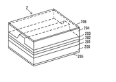
- FIG. 3 is a perspective view of the semiconductor laser according to the first embodiment of the present invention.
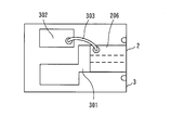
- FIG. 4 is a perspective view illustrating a method of fixing a semiconductor laser to a subcarrier in the first embodiment of the present invention.
- FIG. 5 is a plan view showing a state in which the semiconductor laser is fixed to the subcarrier in the first embodiment of the present invention.
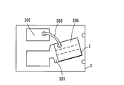
- FIG. 6 is a plan view showing another example in which the semiconductor laser is fixed to the subcarrier in the first embodiment of the present invention.
- FIG. 1 is a perspective view of a planar light wave circuit according to a first embodiment of the present invention.
- FIG. 2 is a plan view of a plane light wave circuit according to the first embodiment of the present invention.
- FIG. 3 is a perspective view of the semiconductor laser according
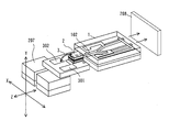
- FIG. 7 is a perspective view illustrating a method of coupling a semiconductor laser and a fringe generation unit in the first embodiment of the present invention.
- FIG. 8 is a plan view showing a state in which the semiconductor laser and the fringe generation unit are coupled in the first embodiment of the present invention.
- FIG. 9 is a plan view showing a coupling portion between the semiconductor laser and the fringe generation portion in the first embodiment of the present invention.
- FIG. 10 is a perspective view illustrating a method of fixing the subcarrier and the fringe generation portion to the ceramic housing in the first embodiment of the present invention.
- FIG. 11 is a cross-sectional view showing a state in which the subcarrier and the fringe generation portion are housed in the ceramic housing in the first embodiment of the present invention.
- FIG. 12 is a plan view showing a state in which the subcarrier and the fringe generating portion are housed in the ceramic housing in the first embodiment of the present invention.
- FIG. 13 is a block diagram showing a configuration for controlling the fringe generation optical module according to the first embodiment of the present invention.
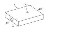
- FIG. 14 is a perspective view showing the appearance of the projection device according to the first embodiment of the present invention.
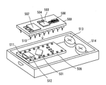
- FIG. 15 is an exploded perspective view showing the internal configuration of the projection device according to the first embodiment of the present invention.
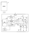
- FIG. 16 is a block diagram showing a configuration of a mobile terminal according to the first embodiment of the present invention.
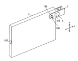
- FIG. 17 is a perspective view illustrating a method of mounting the projection device according to the first embodiment of the present invention on a mobile terminal.
- FIG. 18 is a perspective view illustrating a method of mounting the projection device according to the first embodiment of the present invention on a mobile terminal.
- FIG. 19 is a front view showing a state in which the projection device according to the first embodiment of the present invention is attached to a mobile terminal.
- FIG. 20 is a flowchart illustrating a three-dimensional measurement method according to the first embodiment of the present invention.
- FIG. 21 is a perspective view showing the appearance of the projection device according to the second embodiment of the present invention.
- FIG. 22 is a block diagram showing a configuration of a projection device according to a second embodiment of the present invention.
- FIG. 23 is a perspective view illustrating a method of mounting the projection device according to the second embodiment of the present invention on a mobile terminal.
- FIG. 24 is a flowchart illustrating a three-dimensional measurement method according to a second embodiment of the present invention.
- FIG. 25 is a block diagram showing a configuration of a server device according to a third embodiment of the present invention.
- FIG. 26 is a flowchart illustrating a three-dimensional measurement method according to a third embodiment of the present invention.
- FIG. 27 is a plan view showing a state in which the semiconductor laser and the fringe generation unit are coupled in the fourth embodiment of the present invention.
- FIG. 28 is a block diagram showing a configuration of an optical system used in a conventional phase shift method.
- a three-dimensional measurement of an object can be realized by a phase shift method by using a projection device that generates a striped pattern by interference of two light beams and projects it onto an object, and a portable terminal equipped with a camera. Provide a portable three-dimensional measurement system.
- the projection device consists of a planar lightwave circuit (PLC: Planar Lightwave Circuit) including a phase modulator, and a fringe generator that generates a striped pattern and a phase modulator that controls the phase of the striped pattern to change the phase of the striped pattern. It is provided with a phase control unit for making the device.
- the mobile terminal includes a camera that shoots an object on which a striped pattern is projected, and an image analysis unit that analyzes multiple images taken by the camera with different phases of the striped pattern and calculates the three-dimensional shape data of the object. To prepare for.
- FIG. 1 is a perspective view of the fringe generation unit 1
- FIG. 2 is a plan view of the fringe generation unit 1.
- FIGS. 1 and 2 the inside of the overclad is shown through.
- the fringe generation unit 1 has an input waveguide 102 coupled to a semiconductor laser (not shown) and a Y-branch guide connected to the input waveguide 102 to split light into two on the underclad 101 formed on the silicon substrate 100.
- Phase modulators 106, 107 that modulate the phase of light propagating through the waveguide 103, the two output waveguides 104, 105 connected to the outputs of the Y-branched waveguide 103, and the two output waveguides 104, 105. And are formed.
- the phase modulators 106 and 107 are composed of heaters 108 and 109 composed of conductors formed directly above the output waveguides 104 and 105, respectively.
- a voltage is supplied to the heater 108 via a heater pad 110 made of a conductor connected to one end of the heater 108 and a ground pad 111 made of a conductor connected to the other end of the heater 108, the heater 108 generates heat.
- the heater 109 when a voltage is supplied to the heater 109 via the heater pad 112 made of a conductor connected to one end of the heater 109 and the ground pad 111 connected to the other end of the heater 109, the heater 109 generates heat.
- the phase of the light propagating through the output waveguides 104 and 105 can be phase-modulated by the thermo-optical effect.
- the size of the chip of the fringe generation unit 1 is 0.8 mm in width and 4 mm in length.
- the length of the heaters 108 and 109 of the phase modulators 106 and 107 was set to 1.5 mm.
- FIGS. 1 and 2 the configuration of the fringe generation unit 1 is schematically described, and the dimensions are exaggerated.
- Quartz glass having a thickness of 3 ⁇ m containing Geo 2 was deposited on an underclad 101 made of a thermal oxide film having a thickness of 10 ⁇ m formed on the silicon substrate 100 by using the FHD (Flame. Hydrolysis Deposition) method. At this time, the amount of GeO 2 dopant was adjusted so that the specific refractive index of the core was 0.5%.
- the shapes of the waveguides 102 to 105 were produced by using general photolithography and reactive ion etching. Further, the overclad 113 was formed again by the FHD method.
- the heaters 108 and 109 made of Cr (chromium) having a thickness of 350 nm were deposited on the overclad 113 at the position directly above the output waveguides 104 and 105 by the lift-off method.
- a heat insulating groove 114 was formed in the overclad 113 and the underclad 101 as shown in FIG.
- the overclad 113 and the overclad 113 A light-shielding groove 115 is formed in the underclad 101.
- the description of the heat insulating groove 114 and the light shielding groove 115 is omitted in order to avoid complication. In the following drawings, the description of the heat insulating groove 114 and the light shielding groove 115 will be omitted.
- the light-shielding groove 115 is not always necessary. However, in order to measure the three-dimensional shape of an object more accurately, it is important to take measures against stray light.
- a waveguide may be formed by using pure quartz as the core and using glass doped with boron or fluorine as the clad.
- the quartz-based waveguide is a waveguide widely used in the field of optical communication, and stability, long-term reliability, and mass productivity can be easily obtained.
- the quartz-based waveguide is transparent to the visible region. Therefore, there is an advantage that an inexpensive camera can be used and an inexpensive semiconductor laser widely used in DVD (Digital Versatile Disc) players and the like can be used.
- the material of the waveguide is not limited to quartz.
- a waveguide may be formed of a crystalline material or the like.
- the heaters 108 and 109 may be made of a metal other than chromium.
- a waveguide made of silicon when used, it becomes transparent to light having a wavelength longer than 1200 nm, so that the same effect as the quartz-based waveguide of this example can be obtained.
- the waveguide made of silicon is opaque to the visible region. For this reason, it becomes impossible to use an inexpensive camera, and the device becomes very high-class.
- phase modulators 106 and 107 including heaters 108 and 109 are used.
- a crystalline material is used for a waveguide, it is also possible to modulate the phase of light by using an electro-optic effect in addition to the thermo-optical effect.
- a current flows at the moment when an electric field is applied to the crystal, but since the current does not always flow, the power consumption can be reduced.
- a waveguide using a crystalline material for example, there is a LiNbO 3 waveguide.
- a waveguide using a crystalline material has a higher material cost than quartz.
- FIG. 3 is a perspective view of the semiconductor laser 2.
- the n-type AlGaInP clad layer 201, the active layer 202 composed of MQW (Multiple Quantum Well), the p-type AlGaInP clad layer 203, and the n-type AlInP are placed on the n-type GaAs substrate 200.
- the block layers 204 are sequentially laminated.
- the upper layer of the p-type AlGaInP clad layer 203 has a ridge stripe shape extending in one direction.
- An n-side electrode 205 is formed on the back surface of the n-type GaAs substrate 200.
- a p-side electrode 206 is formed on the n-type AlInP block layer 204.
- the semiconductor laser 2 oscillates at a wavelength in the 650 nm band and is widely used as a generally known light source for DVDs.
- the semiconductor laser 2 is commercially available and can be easily procured. Although the composition and structure differ depending on the manufacturer, it is obvious that the difference in the structure of the semiconductor laser 2 does not matter in the present invention, and other structures may be used.
- the visible semiconductor laser 2 is commercially available that emits light up to the near infrared region, and the wavelength does not have to be in the 650 nm band. Further, the material of the semiconductor laser 2 is not limited to the above example. Since most of the image pickup device is made of silicon, the semiconductor laser 2 can be manufactured at low cost if the wavelength is such that the sensitivity of the image pickup device can be obtained.
- the oscillation wavelength of the semiconductor laser 2 may exceed 1 ⁇ m.
- the oscillation wavelength of the semiconductor laser 2 may exceed 1 ⁇ m.
- a semiconductor laser 2 with an oscillation wavelength of more than 1 ⁇ m if you select eye safe (wavelength that is safe for the eyes), you can measure the human face safely with your eyes open. There are also merits such as.
- FIG. 4 is a perspective view illustrating a method of fixing the semiconductor laser 2 to the subcarrier 3
- FIG. 5 is a plan view showing a state in which the semiconductor laser 2 is fixed to the subcarrier 3.
- the subcarrier 3 is made of a silicon substrate 300 having a thermal oxide film having a thickness of 100 nm on the surface thereof.
- An n-side electrode pad 301 and a p-side electrode pad 302 are formed on the thermal oxide film.
- the semiconductor laser 2 is mounted on the n-side electrode pad 301 of the subcarrier 3 so that the n-side electrode pad 301 and the n-side electrode 205 are in contact with each other.
- the p-side electrode pad 302 of the subcarrier 3 and the p-side electrode 206 of the semiconductor laser 2 are connected by a wire 303.
- the semiconductor laser 2 and the subcarrier 3 are fixed by using a solder sheet.
- the n-side electrode pad 301 of the subcarrier 3 and the n-side electrode 205 of the semiconductor laser 2 may be fixed with a conductive paste or the like.
- the emission end (right end of FIG. 5) of the semiconductor laser 2 and the end of the subcarrier 3 are fixed so as to be in the same position.
- the position was confirmed with a camera at the time of mounting, the positions of the edges were aligned, and then fixed.
- the emission end of the semiconductor laser 2 may be separated from the end of the subcarrier 3 by a distance of 10 ⁇ m or less.
- the end of the subcarrier 3 and the emission end of the semiconductor laser 2 are aligned, but as shown in FIG. 6, the emission end of the semiconductor laser 2 is about 8 degrees with respect to the end of the subcarrier 3. It may be mounted at an angle. The semiconductor laser 2 becomes unstable when the reflected return light is incident. By mounting the emission end of the semiconductor laser 2 at an angle with respect to the end of the subcarrier 3, it is possible to prevent the reflected light from the coupling end surface with the fringe generation unit 1 from returning to the semiconductor laser 2.
- FIG. 7 is a perspective view illustrating a method of coupling the semiconductor laser 2 and the fringe generation unit 1
- FIG. 8 is a plan view showing a state in which the semiconductor laser 2 and the fringe generation unit 1 are coupled.
- a current is supplied to the semiconductor laser 2 via the n-side electrode pad 301 and the p-side electrode pad 302 of the subcarrier 3, and the subcarrier 3 is held by using the pickup tool 207 in a state where the semiconductor laser 2 is oscillated.
- the semiconductor laser 2 and the input waveguide 102 of the fringe generation unit 1 are coupled by an XYZ stage (not shown) equipped with the pickup tool 207.
- a large PD (Photodiode) 208 is arranged on the outlet side of the fringe generation unit 1, and the subcarrier 3 and the fringe generation unit 1 are combined so that the light intensity on the emission side of the fringe generation unit 1 is maximized. Perform alignment.
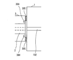
- UV (Ultra Violet) adhesive is poured from both sides into the gap between the subcarrier 3 and the fringe generation unit 1, and UV is irradiated to cure the UV adhesive, and the subcarrier 3 is used. And the fringe generation unit 1 was fixed. As shown in the plan view of FIG. 9, by forming the inflow prevention groove 304 in the end face of the subcarrier 3, it is possible to prevent the UV adhesive 305 from flowing into the end face of the semiconductor laser 2.
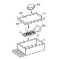
- FIG. 10 is a perspective view illustrating a method of fixing the subcarrier 3 and the fringe generation unit 1 to the ceramic housing 4, and FIG. 11 shows a state in which the subcarrier 3 and the fringe generation unit 1 are housed in the ceramic housing 4.
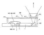
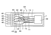
- FIG. 12 is a cross-sectional view showing a plan view showing a state in which the subcarrier 3 and the fringe generation unit 1 are housed in the ceramic housing 4.
- the parts connecting the subcarrier 3 and the fringe generation unit 1 as described above are stored in the ceramic housing 4.
- the subcarrier 3 and the fringe generation unit 1 are housed together with a 45-degree prism 400 for realizing 90-degree optical path conversion of the light emitted from the fringe generation unit 1.
- the fringe generation unit 1 When storing the subcarrier 3 and the fringe generation unit 1, the fringe generation unit 1 is mechanically brought into contact with the 45-degree prism 400 and the fringe generation unit 1 by abutting the fringe generation unit 1 on the side of the 45-degree prism 400 fixed to the ceramic housing 4. Arrange in parallel. The subcarrier 3 and the fringe generation unit 1 are fixed to the ceramic housing 4 with a UV adhesive.
- the heater pad 110 of the fringe generation unit 1 and the electrode pad 401 of the ceramic housing 4 are connected by a wire 402, and the heater pad 112 of the fringe generation unit 1 and the electrode pad 403 of the ceramic housing 4 are connected by a wire 404. Then, the ground pad 111 of the fringe generation unit 1 and the electrode pad 405 of the ceramic housing 4 are connected by a wire 406.
- n-side electrode pad 301 of the subcarrier 3 and the electrode pad 407 of the ceramic housing 4 are connected by a wire 408, and the p-side electrode pad 302 of the subcarrier 3 and the electrode pad 409 of the ceramic housing 4 are connected by a wire 410. Connect with.
- the lid 411 in which the metal frame 413 is formed around the glass 412 by the metallizing method is soldered to the ceramic housing 4, and the ceramic housing 4 is sealed.
- the sealing surface of the ceramic housing 4 is metallized, and the metal on the sealing surface and the frame 413 of the lid 411 are soldered.
- the resin-molded lens 414 was placed on the optical axis of the 45-degree prism 400 and fixed to the glass 412 of the lid 411 with a UV adhesive.
- a concave lens obtained by injection molding of a resin is used, but the present invention is not limited to this, and a ball lens or the like may be used.
- the ceramic housing 4 has a length of 8 mm, a width of 2 mm, and a thickness of 1.5 mm.
- the ceramic housing 4 is used, but the housing may be formed of other materials. Although the ceramic housing 4 is sealed in order to obtain long-term reliability of the device, the sealing of the housing is not an essential constituent requirement in the present invention.
- the 45-degree prism 400 is arranged in order to realize the 90-degree optical path conversion of the light emitted from the fringe generation unit 1, but it is a method of directly forming the 45-degree mirror on the fringe generation unit 1. It doesn't matter. In this case, since the 45-degree mirror can be manufactured by the wafer process, the labor for arranging the 45-degree prisms one by one and the number of member points can be reduced.
- fringe generation optical modules The parts assembled in the above process are hereinafter referred to as fringe generation optical modules.
- the advantage of the fringe generation optical module is that it is manufactured by using PLC, so that the size is smaller than that of the case where it is manufactured by combining micro optical components.
- the fringe generation optical module of this embodiment does not have a moving part, the optical axis does not shift during transportation and is stable. That is, the fringe generation optical module of this embodiment is very small, has excellent portability, and has stability that can withstand movement.
- FIG. 13 is a block diagram showing a configuration for controlling the fringe generation optical module 500.
- the projection device 5 including the fringe generation optical module 500 includes a microcomputer 501, a communication module 502, a control circuit 503 of the heaters 108 and 109 of the fringe generation optical module 500, and n of the semiconductor laser 2 of the fringe generation optical module 500.
- a resistor 507 connected to the side electrode is provided.
- the control circuit 503 is composed of a DA converter (DAC: Digital to Analog converter) 504 and transistors 505 and 506. With the configuration as shown in FIG. 13, the microcomputer 501 can drive the heaters 108 and 109 of the fringe generation optical module 500 via the control circuit 503.
- DAC Digital to Analog converter
- the control circuit 503 is configured so that sufficient power can be obtained via the transistors 505 and 506, but the output power from the DAC 504 can sufficiently drive the heaters 108 and 109. If so, the transistors 505 and 506 are unnecessary.
- the microcomputer 501 is connected to the communication module 502 so that it can wirelessly communicate with the mobile terminal 6 such as a smartphone.
- the mobile terminal 6 such as a smartphone.
- Bluetooth registered trademark
- the microprocessor 501 receives an instruction set from the mobile terminal 6 via the communication module 502.
- the microcomputer 501 can control the light emission and extinguishing of the semiconductor laser 2 by turning on / off the current supplied to the semiconductor laser 2 of the fringe generation optical module 500.
- the microcomputer 501 executes the process described in this embodiment according to a program stored in an internal memory (not shown), and functions as a laser control unit 517 and a phase control unit 518.
- FIG. 14 is a perspective view showing the appearance of the projection device 5
- FIG. 15 is an exploded perspective view showing the internal configuration of the projection device 5.
- the printed circuit board 509 is mounted on the board 508 of the commercially available microcomputer 501.
- a fringe generation optical module 500, a communication module 502, and a control circuit 503 are mounted on the printed circuit board 509.
- the printed circuit board 509 is fixed by inserting the pin 510 of the connector provided on the lower surface of the printed circuit board 509 into the through hole 511 of the board 508 and soldering the circuit board 509. And the circuit on the board 508 are connected.
- a USB (Universal Serial Bus) connector 512 is mounted on the board 501 so that it can communicate with the mobile terminal 6 not only by wireless communication but also by wire. It is said that Bluetooth is used for exchanging signals with the mobile terminal 6, but any other communication technology such as Wi-Fi may be used as long as the signal can be exchanged with the mobile terminal 6, and USB is used. It does not matter if it is a wired communication.
- the board 508 on which the printed circuit board 509 was mounted and the battery 513 as a power source were housed in the plastic case 514.
- the size of the plastic case 514 was 45 mm ⁇ 30 mm ⁇ 5 mm.
- the plastic case 514 is formed with an exit port 515 so that the laser beam from the fringe generation optical module 500 can be taken out, and an opening 516 for exposing the USB connector 512.
- the exit port 515 is located directly above the lens 414 of the fringe generation optical module 500. Therefore, the two luminous fluxes emitted from the output waveguides 104 and 105 of the fringe generation unit 1, reflected by the 45-degree prism 400, and passed through the lens 414 are radiated into space from the exit port 515.
- the power supplied from the mobile terminal 6 can be acquired via the USB connector 512, so that the projection device 5 can be miniaturized, and there is no need to charge the battery 513 or replace the battery 513. Become.
- FIG. 16 is a block diagram showing the configuration of the mobile terminal 6.
- the mobile terminal 6 includes a CPU (Central Processing Unit) 600, a memory 601, a communication circuit 602 for wireless communication with the projection device 5, a USB connector 603 for wired communication, and a communication circuit 604 for wired communication. It includes a display 605 with a touch panel function, a camera 606, and a communication circuit 607 for communication with a server device described later.
- a CPU Central Processing Unit
- memory 601 for wireless communication with the projection device 5
- a USB connector 603 for wired communication
- a communication circuit 604 for wired communication.
- It includes a display 605 with a touch panel function, a camera 606, and a communication circuit 607 for communication with a server device described later.
- the CPU 600 executes the process described in this embodiment according to the program stored in the memory 601, and includes an image acquisition unit 608, a laser control unit 609, a communication unit 610, a phase control unit 611, and an image analysis unit 612. , It functions as a display unit 613, a camera control unit 614, and a communication unit 615.
- 17 and 18 are perspective views illustrating a method of attaching the projection device 5 to the mobile terminal 6. As shown in FIG. 17, the projection device 5 is fixed by being fitted into the opening 701 of the clip-shaped fixture 7 having the metal spring 700.
- the mobile terminal 6 is sandwiched by the fixture 7 equipped with the projection device 5.
- a window glass 703 transparent plate
- the position of the fixture 7 is adjusted so that the window glass 703 covers the light receiving surface of the camera 606 of the mobile terminal 6.
- O in FIG. 19 indicates the center of the light receiving surface of the camera 606.
- a transparent plate made of an organic substance may be provided instead of the window glass 703, a transparent plate made of an organic substance.
- an organic transparent plate it is more easily scratched than glass, but it is possible to reduce the cost.
- FIG. 20 is a flowchart illustrating the three-dimensional measurement method of this embodiment.
- the user of the three-dimensional measurement system attaches the projection device 5 to the mobile terminal 6 by the fixture 7 as described above.
- the projection device 5 is fitted in the fixture 7 so that the exit port 515 faces the same direction as the camera 6 of the mobile terminal 6. Therefore, it is possible to project the striped pattern from the projection device 5 onto the object to be measured and photograph the object with the camera 606.
- the user After attaching the projection device 5 to the mobile terminal 6, the user activates the three-dimensional measurement application and points the camera 606 of the mobile terminal 6 at the object to be measured.
- the image acquisition unit 608 of the mobile terminal 6 activates the camera 606 to enable shooting (step S100 in FIG. 20).
- the laser control unit 609 of the mobile terminal 6 passes a light emission control signal for turning on the semiconductor laser 2 of the projection device 5 to the communication unit 610.
- the communication unit 610 passes the light emission control signal to the communication circuit 602 for wireless communication or the communication circuit 604 for wired communication.
- the communication circuit 602 or 604 transmits a light emission control signal to the projection device 5.
- the microcomputer 501 of the projection device 5 receives the light emission control signal from the mobile terminal 6 via the communication module 502. Further, in the case of wired communication, the microcomputer 501 receives the light emission control signal via the USB connector 512. Upon receiving the light emission control signal from the mobile terminal 6, the laser control unit 517 of the projection device 5 causes the semiconductor laser 2 to emit light (step S101 in FIG. 20).
- the phase control unit 611 of the mobile terminal 6 passes a phase control signal for setting the phase of the striped pattern projected from the projection device 5 to the object to be measured as the initial phase to the communication unit 610.
- the communication unit 610 passes the phase control signal to the communication circuit 602 or 604.
- the communication circuit 602 or 604 transmits a phase control signal to the projection device 5.
- phase control unit 518 of the projection device 5 When the phase control unit 518 of the projection device 5 receives the phase control signal from the mobile terminal 6 via the communication module 502 or the USB connector 512, the phase control unit 518 outputs phase control data indicating the voltage value corresponding to the phase control signal to the DAC 504. ..
- the DAC 504 outputs a voltage corresponding to the phase control data to the transistors 505 and 506. In the case of the initial phase, the voltage applied to the heaters 108 and 109 of the phase modulators 106 and 107 is actually 0. In this way, the phase of the striped pattern projected from the exit port 515 of the projection device 5 onto the object to be measured can be set as the initial phase (step S102 in FIG. 20).
- the image acquisition unit 608 of the mobile terminal 6 acquires an image of an object taken by the camera 606.
- the image of the object is stored in the memory 601 (step S103 in FIG. 20).
- the phase control unit 611 of the mobile terminal 6 shifts the phase of the striped pattern projected on the object to be measured by ⁇ / n (n is an integer of 2 or more) to the communication unit 610. hand over.
- phase control unit 518 of the projection device 5 When the phase control unit 518 of the projection device 5 receives the phase control signal from the mobile terminal 6, it outputs phase control data indicating a voltage value corresponding to the phase control signal to the DAC 504.
- the voltage corresponding to the phase control data is output from the DAC 504 to the transistors 505 and 506, the heaters 108 and 109 of the phase modulators 106 and 107 generate heat, and at least of the light propagating through the output waveguides 104 and 105.
- the phase of one of the lights is phase-modulated by the thermo-optical effect. In this way, the phase of the striped pattern projected from the exit port 515 of the projection device 5 onto the object to be measured can be shifted by ⁇ / n (step S104 in FIG. 20).
- the image acquisition unit 608 of the mobile terminal 6 acquires an image of an object taken by the camera 606 (step S105 in FIG. 20).
- the above steps S104 and S105 are performed n times while shifting the phase of the striped pattern by ⁇ / n.
- n 8.
- n may be 4 or more.
- the image analysis unit 612 of the mobile terminal 6 analyzes (n + 1) images taken by the camera 606 and analyzes the three-dimensional shape of the object to be measured.
- the data is calculated (FIG. 20 step S107). Since the method of calculating the three-dimensional shape data by the phase shift method is a well-known technique, detailed description thereof will be omitted.
- the display unit 613 of the mobile terminal 6 generates a two-dimensional image obtained by projecting a three-dimensional model of an object obtained by the three-dimensional shape data calculated by the image analysis unit 612 onto a projection surface (screen of the mobile terminal 6).
- the generated image is displayed on the display 605 (step S108 in FIG. 20).
- the position of the viewpoint with respect to the three-dimensional model can be freely changed, for example, by the user performing a tracing operation on the screen of the display device 605 with a touch panel function.
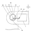
- the accuracy of the three-dimensional measurement of the object is the center of the outlet 515 of the projection device 5 (more accurately, the center of the two light fluxes emitted from the fringe generation optical module 500 of the projection device 5) and the camera 606. It is determined by the distance dx in the x direction and the distance dy in the y direction from the center O of the light receiving surface.
- the projection device 5 is attached to the mobile terminal 6 by using the clip-shaped fixture 7 as described above, there is a problem that the distances dx and dy are difficult to be uniquely determined.
- the window glass 703 of the fixture 7 is formed with scales 704 and 705 in each of the two directions (x-direction and y-direction in FIGS. 18 and 19) orthogonal to the shooting direction of the camera 606.
- the window glass 703 (transparent plate) and the scales 704 and 705 form an alignment structure 706 for determining the relative position between the exit port 515 of the projection device 5 and the camera 606 of the mobile terminal 6.
- the intervals between the scales 704 and 705 are set to 500 ⁇ m.
- the scales 704 and 705 are printed on the window glass 703 using screen printing technology, they may be produced by other methods such as laser processing.
- the effect of the alignment structure 706 of this embodiment will be described.
- the user adjusts the position of the fixture 7 so that the center position of the window glass 703 of the fixture 7 is approximately the center position of the light receiving surface of the camera 606 of the mobile terminal 6.
- the distances dx and dy between the center of the exit port 515 of the projection device 5 and the center of the light receiving surface of the camera 606 can be set to approximately the desired value, and more accurate three-dimensional measurement can be performed. can.
- the user can know some distances dx and dy from the image based on the scales 704 and 705 shown in the image. .. As a result, the distances dx and dy can be known accurately, and the accuracy of the three-dimensional measurement can be improved.
- a camera may be mounted on the projection device.
- the appearance of the projection device 5a in this case is shown in FIG. 21, and the configuration of the projection device 5a is shown in FIG. 22.
- the microcomputer 501 of the projection device 5a executes the process described in this embodiment according to a program stored in an internal memory (not shown), and controls the laser control unit 517, the phase control unit 518, and the camera 519. It functions as a camera control unit 520.
- the USB connector 512 of the projection device 5 is a female connector.
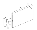
- the male USB connector 512a (first connector) is used by inserting it into the USB connector 603 (second connector) of the mobile terminal 6. .. That is, in this embodiment, the signal exchange between the projection device 5a and the mobile terminal 6 is performed by wire communication.
- the configuration of the mobile terminal 6 is the same as that of the first embodiment.
- FIG. 24 is a flowchart illustrating the three-dimensional measurement method of this embodiment.
- the user activates the three-dimensional measurement application and points the camera 519 of the projection device 5a at the object to be measured.
- the camera control unit 614 of the mobile terminal 6 passes the camera activation control signal to the communication unit 610.
- the communication unit 610 passes the camera activation control signal to the communication circuit 604 for wired communication.
- the communication circuit 604 transmits a camera activation control signal to the projection device 5a.
- the camera control unit 520 of the projection device 5a When the camera control unit 520 of the projection device 5a receives the camera activation control signal via the USB connector 512a, the camera control unit 520 activates the camera 519 to enable shooting (step S100a in FIG. 24).
- steps S101 and S102 in FIG. 24 is the same as that of the first embodiment.
- the image acquisition unit 608 of the mobile terminal 6 passes the image request signal to the communication unit 610.
- the communication unit 610 passes the image request signal to the communication circuit 604.
- the communication circuit 604 transmits an image request signal to the projection device 5a.
- the camera control unit 520 of the projection device 5a When the camera control unit 520 of the projection device 5a receives the image request signal via the USB connector 512a, the camera control unit 520 transmits the image of the object captured by the camera 519 to the mobile terminal 6 via the USB connector 512a.
- the image acquisition unit 608 of the mobile terminal 6 acquires an image transmitted from the projection device 5a (step S103a in FIG. 24).
- steps S104 and S106 to S108 in FIG. 24 are the same as that of the first embodiment.
- the process of step S105a in FIG. 24 is the same as that of step S103a.
- the three-dimensional measurement of the object can be performed by using the dedicated camera 519 of the projection device 5a.
- the distance between the center of the exit port 515 and the center of the light receiving surface of the camera 519 can be made constant. Therefore, highly accurate three-dimensional measurement is possible.
- the camera 519 is mounted on the projection device 5a in addition to the camera 606 that is standardly mounted on the mobile terminal 6, there is a demerit that the cost increases.
- the captured image was analyzed by the image analysis unit 612 of the mobile terminal 6, and the three-dimensional shape data of the object was calculated.
- the captured image data and the measurement conditions may be transmitted to a dedicated server device, the three-dimensional shape data of the object may be calculated by the server device, and the calculation result may be sent back to the mobile terminal 6.
- the configuration of the server device of this embodiment is shown in FIG.
- the server device 8 includes a CPU 800, a memory 801 and a communication circuit 802 for wireless communication.
- the CPU 800 executes the process described in this embodiment according to the program stored in the memory 801 and functions as the communication unit 803 and the image analysis unit 804.
- the configurations of the projection devices 5 and 5a and the mobile terminal 6 are the same as those of the first and second embodiments.
- FIG. 26 is a flowchart illustrating the three-dimensional measurement method of this embodiment.
- the processing of steps S100 to S106 of FIG. 26 is the same as that of the first embodiment.
- the communication unit 615 of the mobile terminal 6 passes the image data of the photographed object and the measurement condition information (such as the phase information of the striped pattern) to the communication circuit 607.
- the communication circuit 607 wirelessly transmits the image data and the measurement condition information to the server device 8 (step S109 in FIG. 26).
- the communication unit 803 of the server device 8 passes the image data received from the mobile terminal 6 and the measurement condition information to the image analysis unit 804 via the communication circuit 802 (step S110 in FIG. 26).
- the image analysis unit 804 analyzes the received image and calculates the three-dimensional shape data of the object to be measured (step S111 in FIG. 20).
- the processing of the image analysis unit 804 is the same as the processing of the image analysis unit 612 of the mobile terminal 6.
- the communication unit 803 of the server device 8 passes the three-dimensional shape data calculated by the image analysis unit 804 to the communication circuit 802.
- the communication circuit 802 transmits the three-dimensional shape data to the mobile terminal 6 (step S112 in FIG. 26).
- the communication unit 615 of the mobile terminal 6 passes the three-dimensional shape data received from the server device 8 via the communication circuit 607 to the display unit 613 (step S113 in FIG. 26).
- the display unit 613 displays an image of the object on the display 605 in the same manner as described above (step S114 in FIG. 26).
- server device 8 of this embodiment is applied to the first embodiment, but it goes without saying that the server device 8 may be applied to the second embodiment.
- the server device 8 When the server device 8 is used as in the present embodiment, if the communication speed between the mobile terminal 6 and the server device 8 is sufficiently obtained, the processing of the mobile terminal 6 can be reduced, and the mobile terminal 6 can be reduced. Power consumption can be reduced. As a result, the battery consumption of the mobile terminal 6 can be suppressed.
- the fringe generation unit 1 described in the first to third embodiments the light source composed of the semiconductor laser 2, the input waveguide 102, the Y-branch waveguide 103, the phase modulators 106, 107, and the output waveguides 104, 105 are used. Are arranged almost in a straight line.
- the coupling loss is, for example, about 2.5 dB, and about half of the light is emitted without being coupled to the input waveguide 102, resulting in stray light.
- a striped pattern whose intensity is spatially sinusically modulated by the interference of two light fluxes emitted from the output waveguides 104 and 105 can be obtained.
- the stray light reaches the exit port 515 of the projection devices 5, 5a and is emitted into the space from the exit port 515, unexpected interference between the striped pattern and the stray light occurs, and the three-dimensional shape data of the object is calculated. The error will be large.
- the fringe generation unit 1a of the present embodiment has the incident direction of light from the semiconductor laser 2 to the input waveguide 102 (y direction in FIG. 27) and the light from the output waveguides 104 and 105.
- the input waveguide 102 bends in the plane of the silicon substrate so as to intersect with the emission direction (x direction in FIG. 27).
- the difference in the specific refractive index of the optical waveguide is 1%, and the bending radius of the input waveguide 102 is 1 mm.
- the method for manufacturing the fringe generation unit 1a, the method for coupling with the semiconductor laser 2, and the method for modularizing the fringe generation unit 1a and the semiconductor laser 2 are the same as those in the first embodiment.
- the emitted light from the semiconductor laser 2 is quartz-based.
- the stray light generated as a coupling loss due to the mismatch of the mode fields is hardly emitted from the output waveguides 104 and 105. Therefore, when two light fluxes are emitted from the projection device into space, a sine-modulated striped pattern can be obtained.
- the fringe generation unit 1a is manufactured so that the incident direction of the light from the semiconductor laser 2 to the input waveguide 102 and the emission direction of the light from the output waveguides 104 and 105 are orthogonal to each other.
- the angle ⁇ of the inclination of the light emitted from the output waveguides 104 and 105 with respect to the incident direction of the light from the semiconductor laser 2 to the input waveguide 102 is approximately 30 degrees or more. If this is the case, stray light will not be emitted from the output waveguides 104 and 105, and an ideally sinusoidally modulated striped pattern can be obtained.
- Examples of using an optical waveguide to generate a striped pattern have been conventionally proposed, but in each example, an optical fiber is used.
- the inventor has a configuration in which a striped pattern whose intensity is spatially and sinusically modulated by two-ray beam interference is obtained, and when stray light is emitted into space from the outlet of the output waveguide, the original striped pattern is unexpected. It was found for the first time that the result of overlapping light and darkness occurs and the accuracy of three-dimensional measurement by the phase shift method decreases.
- the inventor has a striped pattern in which the intensity changes in a sinusoidal manner close to the ideal by crossing the incident direction of the light from the semiconductor laser to the input waveguide and the exit direction of the light from the output waveguide as described above. was found for the first time to be obtained.
- the present invention can be applied to a technique for measuring a three-dimensional shape of an object by a phase shift method.
- Communication Module 503 ... control circuit, 504 ... DA converter, 505 ... transistor, 508 ... board, 509 ... printed board, 510 ... pin, 511 ... through hole, 512,512a ... USB connector, 513 ... battery, 514 ... plastic Case, 515 ... Exit port, 517 ... Laser control unit, 518 ... Phase control unit, 519,606 ... Camera, 520 ... Camera control unit, 600,800 ... CPU, 601,801 ... Memory, 602,604,607,802 ... communication circuit, 603 ... USB connector, 605 ... display, 606 ... camera, 608 ... image acquisition unit, 609 ... laser control unit, 610,615,803 ... communication unit, 611 ... phase control unit, 612,804 ... image Analysis unit, 613 ... Display unit, 614 ... Camera control unit, 703 ... Window glass, 704, 705 ... Scale, 706 ... Alignment structure.
Landscapes
- Physics & Mathematics (AREA)
- General Physics & Mathematics (AREA)
- Engineering & Computer Science (AREA)
- Computer Vision & Pattern Recognition (AREA)
- Nonlinear Science (AREA)
- Optics & Photonics (AREA)
- Length Measuring Devices By Optical Means (AREA)
- Optical Modulation, Optical Deflection, Nonlinear Optics, Optical Demodulation, Optical Logic Elements (AREA)
Abstract
3次元計測システムは、2光束の干渉により縞模様を発生させて物体に投影する投影装置(5)と、携帯端末(6)とを備える。投影装置(5)は、位相変調器を含む平面光波回路からなり、縞模様を発生させるフリンジ生成部と、位相変調器を制御して縞模様の位相を変化させる位相制御部とを備える。携帯端末(6)は、縞模様が投影された物体を撮影するカメラ(606)と、カメラ(606)によって撮影された、縞模様の位相が異なる複数枚の画像を解析して、物体の3次元形状データを計算する画像解析部とを備える。
Description
本発明は、位相シフト法により物体の3次元形状を計測する3次元計測システムに係り、特に小型で可搬性に優れ、安定的に計測できる3次元計測システムに関するものである。
近年、3Dプリンタの発展により、物作りの手法は大きな変革を迎えている。3Dプリンタを使用するためには、物体の3次元情報を詳細に調べることが重要であり、3次元の計測技術が着目されている。また、車体などの凹凸の検査等、製造現場における3次元計測の必要性は非常に高い。
さらに、近年では画像認識によりスマートフォンのロックを解除したり、ATM(Automatic Teller Machine)の操作を可能にしたりする個人認証技術が着目されている。このような個人認証の分野において、第三者による成り済ましに対する対策として、人の3次元計測データを同時に取得しようという動きがある。
物体の3次元形状を非接触で測定する方法の一つとして、位相シフト法がある。位相シフト法は、光強度が空間的に正弦波状の縞模様を計測対象物体に投影し、光の位相を少なくとも3回シフトさせ、投影方向とは別の角度から物体を撮影することにより、投影されたパターンの位相値を算出し、位相値から物体の表面形状を求める方法である。位相シフト法は、撮像素子の各計測点で物体の形状(変位)の高さの変位量が計測でき、3次元形状を求めることができる方法である。
位相シフト法では、2光束を干渉させて、縞模様を計測対象の物体に投影する。2光束を干渉させるために、2つの光路の一方には光の位相を変化させる位相シフト機構が設けられる。位相シフト法で使用される光学系としては、通常、図28のような構成を用いている。
レーザ1000から出力された光は、透過率50%のハーフミラー1001によって光路が2つに分割される。ハーフミラー1001によって分割された一方の光は、ミラー1002によって反射され、さらにハーフミラー1001によって反射されて、レンズ1003によって集光され物体1010に入射する。
ハーフミラー1001によって分割された他方の光は、ピエゾ素子等の機械的な変位機構1005を有するミラー1004に入射し、ミラー1004によって反射され、ハーフミラー1001とレンズ1003を通過して物体1010に入射する。物体1010からの反射光は、レンズ1006を通過してCCD1007に入射する。
変位機構1005によりミラー1004を変位させることで他方の光の光路長が変化する。この光路長の変化により2つの光が干渉し、縞模様が物体1010上に投影されることになる。また、ミラー1004の位置を変えることで、干渉により縞が移動することになる。
位相が異なるそれぞれの縞模様をCCD1007で撮影し、撮影した縞模様の位相をCCD1007の画素毎に計算することにより、物体1010上の縞模様の変位量を求めることができ、最終的に物体1010の3次元形状を得ることができる。
図28に示したように、従来の位相シフト法で用いられる光学系は、単体の光学部品を組み合わせたものであり、構成が煩雑で部品点数が多く、装置全体が大きくなり可搬性が劣るという課題があった。
一方、特許文献1には、光学系を小型化する方法が開示されている。しかしながら、特許文献1に開示された構成では、単体の光学部品を組み合わせる点で図28の構成と変わりがなく、光学系の小型化には限界があった。また、特許文献1に開示された構成では、ピエゾ素子からなる可動部を有するため安定性に欠け、経年により状態が変化してしまうという課題があった。
光学系の更なる小型化を目指す構成として、非特許文献1に光ファイバーを用いた構成が開示されている。非特許文献1に開示された構成では、レーザから出力された光をスプリッターで2分岐させ、分岐させた光をそれぞれファイバーを介して物体に照射する。一方のファイバーに設けた可変波長板によって光の位相シフトを実現している。
非特許文献1に開示された構成では、ファイバーは標準的なものであればジャケット(被覆)を含めても直径が1mmもないため、2本使用しても2mm程度の幅で済み、光学系の小型化が可能である。しかしながら、非特許文献1に開示された構成では、スプリッターの後のファイバーが動くことにより、2本の光路長が意図せずに変動してしまい、安定的に測定できないという課題があった。
小型化と計測精度の低下抑制とを目的とする方法として、特許文献2に開示されているように平面光波回路を用いる方法がある。平面光波回路を用いることで、Y分岐スプリッターと位相変調器を集積化することができ、安定的な縞の投影と位相制御とを僅か数ミリの大きさで実現することができる。また、特許文献2に開示された構成では、物体を撮影する小型のカメラを平面光波回路に固定し、平面光波回路の配線部と電気的に接続するようにしている。
しかしながら、特許文献2に開示された構成で想定される利用分野は内視鏡などである。非特許文献1、特許文献2に開示された構成では、ファイバーの長手方向のサイズが数m程度になるので、可搬性と安定性が欠けていると言わざる得ない。
Silvio Pulwer,P.Steglich,C.Villringer,J.Bauer,T.Reusch,S.Schrader,"Fiber-optic interference fringe projection for 3D measurement",DGaO-Proceedings,2016,<https://www.dgao-proceedings.de/download/117/117_p23.pdf>
本発明は、上記課題を解決するためになされたもので、小型で可搬性に優れ、安定的に計測が可能な3次元計測システムを提供することを目的とする。
本発明の3次元計測システムは、2光束の干渉により縞模様を発生させて物体に投影するように構成された投影装置と、携帯端末とを備え、前記投影装置は、位相変調器を含む平面光波回路からなり、前記縞模様を発生させるように構成されたフリンジ生成部と、前記位相変調器を制御して前記縞模様の位相を変化させるように構成された位相制御部とを備え、前記携帯端末は、前記縞模様が投影された物体を撮影するように構成されたカメラと、前記カメラによって撮影された、前記縞模様の位相が異なる複数枚の画像を解析して、前記物体の3次元形状データを計算するように構成された画像解析部とを備えることを特徴とするものである。
また、本発明の3次元計測システムの1構成例において、前記フリンジ生成部は、光源と、前記光源の出力と結合する入力導波路と、前記入力導波路に接続され光を2分岐させるように構成されたY分岐導波路と、前記Y分岐導波路の出力に接続された2本の出力導波路と、前記2本の出力導波路にそれぞれ設けられ、前記2本の出力導波路を伝搬する光の位相を変調するように構成された2つの前記位相変調器とを備えることを特徴とするものである。
また、本発明の3次元計測システムの1構成例において、前記入力導波路は、前記光源から前記入力導波路への光の入射方向に対する前記出力導波路からの光の出射方向の傾きの角度が30度以上となるように中途で曲がることを特徴とするものである。
また、本発明の3次元計測システムの1構成例は、前記携帯端末を挟み込むクリップ状の固定具をさらに備え、前記投影装置は、前記固定具に固定され、前記固定具は、前記投影装置の前記2光束の出射口と前記携帯端末のカメラとの相対位置を定めるための位置合わせ構造を備えることを特徴とするものである。
また、本発明の3次元計測システムの1構成例において、前記位置合わせ構造は、前記固定具が前記携帯端末に装着されたときに前記携帯端末のカメラの受光面を覆うように前記固定具に配設された透明板と、前記透明板に形成された目盛りとから構成されることを特徴とするものである。
また、本発明の3次元計測システムの1構成例において、前記入力導波路は、前記光源から前記入力導波路への光の入射方向に対する前記出力導波路からの光の出射方向の傾きの角度が30度以上となるように中途で曲がることを特徴とするものである。
また、本発明の3次元計測システムの1構成例は、前記携帯端末を挟み込むクリップ状の固定具をさらに備え、前記投影装置は、前記固定具に固定され、前記固定具は、前記投影装置の前記2光束の出射口と前記携帯端末のカメラとの相対位置を定めるための位置合わせ構造を備えることを特徴とするものである。
また、本発明の3次元計測システムの1構成例において、前記位置合わせ構造は、前記固定具が前記携帯端末に装着されたときに前記携帯端末のカメラの受光面を覆うように前記固定具に配設された透明板と、前記透明板に形成された目盛りとから構成されることを特徴とするものである。
また、本発明の3次元計測システムは、2光束の干渉により縞模様を発生させて物体に投影するように構成された投影装置と、携帯端末とを備え、前記投影装置は、位相変調器を含む平面光波回路からなり、前記縞模様を発生させるように構成されたフリンジ生成部と、前記位相変調器を制御して前記縞模様の位相を変化させるように構成された位相制御部と、前記縞模様が投影された物体を撮影するように構成されたカメラと、前記カメラによって撮影された画像を前記携帯端末に送信するように構成された第1の通信部と、前記携帯端末との通信用の第1のコネクタとを備え、前記携帯端末は、前記投影装置から画像を受信するように構成された第2の通信部と、前記投影装置のカメラによって撮影された、前記縞模様の位相が異なる複数枚の画像を解析して、前記物体の3次元形状データを計算するように構成された画像解析部と、前記投影装置との通信用の第2のコネクタとを備え、前記投影装置は、前記第1のコネクタと前記第2のコネクタとが嵌合することにより、前記携帯端末に装着されることを特徴とするものである。
また、本発明の3次元計測システムの1構成例において、前記フリンジ生成部は、光源と、前記光源の出力と結合する入力導波路と、前記入力導波路に接続され光を2分岐させるように構成されたY分岐導波路と、前記Y分岐導波路の出力に接続された2本の出力導波路と、前記2本の出力導波路にそれぞれ設けられ、前記2本の出力導波路を伝搬する光の位相を変調するように構成された2つの前記位相変調器とを備えることを特徴とするものである。
また、本発明の3次元計測システムの1構成例において、前記入力導波路は、前記光源から前記入力導波路への光の入射方向に対する前記出力導波路からの光の出射方向の傾きの角度が30度以上となるように中途で曲がることを特徴とするものである。
また、本発明の3次元計測システムの1構成例において、前記入力導波路は、前記光源から前記入力導波路への光の入射方向に対する前記出力導波路からの光の出射方向の傾きの角度が30度以上となるように中途で曲がることを特徴とするものである。
本発明によれば、投影装置に、位相変調器を含む平面光波回路からなるフリンジ生成部と、位相制御部とを設け、携帯端末にカメラと画像解析部とを設けることにより、小型で可搬性に優れ、安定的に計測が可能な3次元計測システムを実現することができる。
また、本発明では、位相変調器を含む平面光波回路からなるフリンジ生成部と、位相制御部と、カメラと、第1の通信部と、第1のコネクタとを設け、携帯端末に第2の通信部と画像解析部と第2のコネクタとを設けることにより、小型で可搬性に優れ、安定的に計測が可能な3次元計測システムを実現することができる。本発明では、記投影装置の2光束の出射口とカメラの受光面の中心との距離を一定にすることができる。
[第1の実施例]
以下、本発明の実施例について図面を参照して説明する。本実施例では、2光束の干渉により縞模様を発生させて物体に投影する投影装置と、カメラを備えた携帯端末とを用いて、位相シフト法により物体の3次元計測を実現することができる可搬性の3次元計測システムを提供する。
以下、本発明の実施例について図面を参照して説明する。本実施例では、2光束の干渉により縞模様を発生させて物体に投影する投影装置と、カメラを備えた携帯端末とを用いて、位相シフト法により物体の3次元計測を実現することができる可搬性の3次元計測システムを提供する。
具体的には、投影装置は、位相変調器を含む平面光波回路(PLC:Planar Lightwave Circuit)からなり、縞模様を発生させるフリンジ生成部と、位相変調器を制御して縞模様の位相を変化させる位相制御部とを備える。携帯端末は、縞模様が投影された物体を撮影するカメラと、カメラによって撮影された、縞模様の位相が異なる複数枚の画像を解析して物体の3次元形状データを計算する画像解析部とを備える。
まず、PLCからなるフリンジ生成部について説明する。図1はフリンジ生成部1の斜視図、図2はフリンジ生成部1の平面図である。なお、図1、図2では、オーバークラッドの内部を透視して記載している。
フリンジ生成部1は、シリコン基板100上に形成されたアンダークラッド101の上に、図示しない半導体レーザと結合される入力導波路102と、入力導波路102に接続され光を2分岐させるY分岐導波路103と、Y分岐導波路103の出力に接続された2本の出力導波路104,105と、2本の出力導波路104,105を伝搬する光の位相を変調する位相変調器106,107とが形成されている。
位相変調器106,107は、それぞれ出力導波路104,105の直上に形成された導体からなるヒータ108,109によって構成される。ヒータ108の一端に接続された導体からなるヒータパッド110と、ヒータ108の他端に接続された導体からなるグランドパッド111を介してヒータ108に電圧が供給されると、ヒータ108が発熱する。
同様に、ヒータ109の一端に接続された導体からなるヒータパッド112と、ヒータ109の他端に接続されたグランドパッド111を介してヒータ109に電圧が供給されると、ヒータ109が発熱する。
このように、ヒータ108,109を発熱させて出力導波路104,105を加熱することにより、出力導波路104,105を伝搬する光の位相を熱光学効果により位相変調することができる。
フリンジ生成部1のチップのサイズは横幅0.8mm、長さ4mmである。位相変調器106,107のヒータ108,109の長さを1.5mmとした。なお、図1、図2では、フリンジ生成部1の構成を模式的に記載しており、寸法を誇張して記載している。
次に、フリンジ生成部1の具体的な製造方法について説明する。シリコン基板100上に形成された厚さ10μmの熱酸化膜からなるアンダークラッド101の上に、GeO2を含有する厚さ3μmの石英ガラスをFHD(Flame. Hydrolysis Deposition)法を用いて堆積した。このとき、コアの比屈折率が0.5%になるようにGeO2のドーパント量を調整した。
その後、一般的なフォトリソグラフィー、リアクティブイオンエッチングを用いて導波路102~105の形状を作製した。さらに、再度FHD法によってオーバークラッド113を形成した。
そして、出力導波路104,105の直上の位置のオーバークラッド113上に、リフトオフ法によって厚さ350nmのCr(クロム)からなるヒータ108,109を蒸着した。熱光学効果が効率よく発現するようにするために、図2に示すようにオーバークラッド113およびアンダークラッド101には、断熱溝114を形成した。
また、半導体レーザと入力導波路102との結合時に結合しきれなかった光やカップラー損失により発生した迷光が出力導波路104,105の出射口にできるだけ出ないようにするために、オーバークラッド113およびアンダークラッド101には遮光溝115を形成してある。なお、図1では、煩雑性を避けるために、断熱溝114と遮光溝115の記載を省略している。以降の図面についても断熱溝114と遮光溝115の記載を省略する。
本来、2光束干渉により強度が空間的に正弦的に変調された縞模様が得られる。しかし、迷光が出力導波路104,105の出射口から空間に放出されると、予期せぬ干渉が発生し、本来の縞模様にさらに周期の異なる縞模様が重ね合わせられた干渉縞が物体に投影されてしまう。その結果、画像解析をして物体の3次元データを演算する際の測定誤差が大きくなってしまう。
このような測定誤差はソフトウェアによってある程度は補正が可能であるため、必ずしも遮光溝115は必要ではない。しかし、物体の3次元形状をより精度良く測定するためには、迷光対策は重要である。
本実施例では、コアドーパントにGeO2を用いているが、他のドーパントであっても無論問題はない。また、コアを純粋な石英とし、ボロンやフッ素をドープしたガラスをクラッドに用いることで導波路を形成してもよい。
石英系導波路は、光通信の分野において広く用いられている導波路であり、安定性、長期信頼性、量産性が容易に得られる。また、石英系導波路は、可視域に対して透明である。このため、安価なカメラを利用することができ、DVD(Digital Versatile Disc)プレーヤなどで普及している安価な半導体レーザを利用することができるという利点がある。
導波路の材料も石英に限るものではないことは言うまでもない。結晶材料などで導波路を形成してもよい。また、ヒータ108,109はクロム以外の金属であってもよい。例えばシリコンからなる導波路を用いた場合、波長が1200nmより長い光に対して透明となるため、本実施例の石英系導波路と同じ効果が得られるので、本実施例の導波路の代わりにシリコンからなる導波路を利用することも原理上はできる。しかしながら、シリコンからなる導波路は可視域に対して不透明である。このため、安価なカメラを利用することができなくなり、装置が非常に高級なものとなってしまう。
本実施例においては、ヒータ108,109からなる位相変調器106,107を用いた。一方、結晶材料を導波路に用いる場合には、熱光学効果以外に、電気光学効果を利用して光の位相を変調することも可能である。
電気光学効果を利用する場合、結晶に電界をかける瞬間に電流が流れるが、常時電流が流れることがないため、消費電力を小さくできる。結晶材料を用いた導波路としては、例えばLiNbO3導波路がある。ただし、結晶材料を用いた導波路は、石英よりも材料コストが高くなってしまう。
次に、光源となる半導体レーザについて述べる。図3は半導体レーザ2の斜視図である。半導体レーザ2においては、n型GaAs基板200上に、n型AlGaInPクラッド層201と、MQW(Multiple Quantum Well:多重量子井戸)からなる活性層202と、p型AlGaInPクラッド層203と、n型AlInPブロック層204が順次積層されている。
p型AlGaInPクラッド層203の上層部は、一方向に延びるリッジストライプ形状を有している。n型GaAs基板200の裏面には、n側電極205が形成されている。n型AlInPブロック層204の上には、p側電極206が形成されている。
半導体レーザ2は、650nm帯の波長で発振し、一般的に知られるDVD用の光源として広く用いられるものである。半導体レーザ2は、市販されており、容易に調達することが可能である。製造メーカにより組成、構造が違うが、本発明において半導体レーザ2の構造の違いは問題でなく、他の構造であってもよいことは自明である。
可視用の半導体レーザ2は、近赤外域まで発光するものが市販されており、波長は650nm帯でなくても構わない。また、半導体レーザ2の材料も上記の例に限定されない。撮像素子の多くがシリコンからなるため、撮像素子の感度が得られる波長であれば、半導体レーザ2を安価に製造することができる。
化合物半導体からなる撮像素子を用いる場合には、半導体レーザ2の発振波長が1μmを超えるものでも構わない。発振波長が1μmを超える半導体レーザ2を用いる場合、アイセーフ(目に入れても安全な波長)などを選択すれば、人体の顔を測定する際に目を開けた状態でかつ安全に計測ができる等のメリットもある。
図4は半導体レーザ2をサブキャリア3に固定する方法を説明する斜視図、図5は半導体レーザ2をサブキャリア3に固定した状態を示す平面図である。
サブキャリア3は、表面に厚さ100nmの熱酸化膜を有するシリコン基板300からなる。熱酸化膜の上には、n側電極パッド301と、p側電極パッド302とが形成されている。
サブキャリア3は、表面に厚さ100nmの熱酸化膜を有するシリコン基板300からなる。熱酸化膜の上には、n側電極パッド301と、p側電極パッド302とが形成されている。
図4、図5に示すようにサブキャリア3のn側電極パッド301上に、n側電極パッド301とn側電極205とが接するように半導体レーザ2が搭載される。サブキャリア3のp側電極パッド302と半導体レーザ2のp側電極206との間は、ワイヤ303によって接続される。
本実施例においては、半導体レーザ2とサブキャリア3とは半田シートを使って固定した。サブキャリア3のn側電極パッド301と半導体レーザ2のn側電極205との通電ができれば、導電ペースト等による固定でもよい。
図5の例では、半導体レーザ2の出射端(図5の右端)とサブキャリア3の端の位置とが同じになるように固定している。実際の製造過程では、搭載時にカメラで位置を確認して端の位置を揃えてから固定した。サブキャリア3の端から半導体レーザ2の出射端が10μm以下の距離で離れていても構わない。ただし、サブキャリア3の端と半導体レーザ2の出射端とを揃えた方がフリンジ生成部1と半導体レーザ2との結合を得る際に、毎回同じ作業で同じ結合が得易いため好ましい。
また、本実施例では、サブキャリア3の端と半導体レーザ2の出射端とを揃えているが、図6に示すように半導体レーザ2の出射端をサブキャリア3の端に対して8度程度傾けて搭載するようにしてもよい。半導体レーザ2は、反射戻り光が入射すると不安定になる。半導体レーザ2の出射端をサブキャリア3の端に対して傾けて搭載することにより、フリンジ生成部1との結合端面からの反射光が半導体レーザ2に戻ることを防ぐことができる。
図7は半導体レーザ2とフリンジ生成部1との結合方法を説明する斜視図、図8は半導体レーザ2とフリンジ生成部1とを結合した状態を示す平面図である。
サブキャリア3のn側電極パッド301とp側電極パッド302とを介して半導体レーザ2に電流を供給し、半導体レーザ2を発振させた状態で、ピックアップツール207を用いてサブキャリア3を保持し、ピックアップツール207を搭載したXYZステージ(不図示)によって半導体レーザ2とフリンジ生成部1の入力導波路102との結合を行う。
サブキャリア3のn側電極パッド301とp側電極パッド302とを介して半導体レーザ2に電流を供給し、半導体レーザ2を発振させた状態で、ピックアップツール207を用いてサブキャリア3を保持し、ピックアップツール207を搭載したXYZステージ(不図示)によって半導体レーザ2とフリンジ生成部1の入力導波路102との結合を行う。
この結合に際しては、フリンジ生成部1の出口側に大型のPD(Photodiode)208を配置し、フリンジ生成部1の出射側の光強度が最大になるようにサブキャリア3とフリンジ生成部1との位置合わせを行う。
光強度が最大になった位置で、サブキャリア3とフリンジ生成部1との隙間に両側からUV(Ultra Violet)接着剤を流し込み、UVを照射をしてUV接着剤を硬化させ、サブキャリア3とフリンジ生成部1の固定を行った。図9の平面図で示すように、サブキャリア3の端面に流れ込み防止溝304を形成しておくことにより、半導体レーザ2の端面にUV接着剤305が流れ込むことを防止することができる。
図10はサブキャリア3とフリンジ生成部1とをセラミック筐体4に固定する方法を説明する斜視図、図11はサブキャリア3とフリンジ生成部1とをセラミック筐体4内に収めた状態を示す断面図、図12はサブキャリア3とフリンジ生成部1とをセラミック筐体4内に収めた状態を示す平面図である。
上記のようにサブキャリア3とフリンジ生成部1とを接続した部品を、セラミック筐体4内に収納する。セラミック筐体4内には、サブキャリア3とフリンジ生成部1と共に、フリンジ生成部1からの出射光の90度の光路変換を実現するための45度プリズム400を収納する。
サブキャリア3とフリンジ生成部1の収納に際して、セラミック筐体4に固定された45度プリズム400の辺にフリンジ生成部1を突き当てることで機械的に45度プリズム400とフリンジ生成部1とを平行に配置する。サブキャリア3とフリンジ生成部1とは、UV接着剤によってセラミック筐体4に固定される。
その後、フリンジ生成部1のヒータパッド110とセラミック筐体4の電極パッド401とをワイヤ402によって接続し、フリンジ生成部1のヒータパッド112とセラミック筐体4の電極パッド403とをワイヤ404によって接続し、フリンジ生成部1のグランドパッド111とセラミック筐体4の電極パッド405とをワイヤ406によって接続する。
さらに、サブキャリア3のn側電極パッド301とセラミック筐体4の電極パッド407とをワイヤ408によって接続し、サブキャリア3のp側電極パッド302とセラミック筐体4の電極パッド409とをワイヤ410によって接続する。
ガラス412の周囲にメタライズ法によって金属の枠413を形成した蓋411をセラミック筐体4に半田付けし、セラミック筐体4の封止を行う。セラミック筐体4のシール面にはメタライズ処理が施されており、シール面の金属と蓋411の枠413とを半田付けする。
封止後に、樹脂成型されたレンズ414を45度プリズム400の光軸上に配置し、UV接着剤によって蓋411のガラス412に固定した。レンズ414としては、樹脂の射出成型により得られた凹型のレンズを用いたが、これに限るものではなく、ボールレンズ等であってもよい。セラミック筐体4は、長さが8mm、幅が2mm、厚さが1.5mmとした。
本実施例では、セラミック筐体4を用いたが、その他の材料によって筐体が形成されていてもよい。デバイスの長期的信頼性を得るためにセラミック筐体4を封止しているが、本発明において筐体の封止は必須の構成要件ではない。
また、本発明では、フリンジ生成部1からの出射光の90度の光路変換を実現するために45度プリズム400を配置したが、45度ミラーをフリンジ生成部1に直接形成する方法であっても構わない。この場合は、ウエハープロセスで45度ミラー作製することができるため、45度プリズムを1つ1つ配置する手間と部材点数とを削減することができる。
以上の工程で組みあがった部品をフリンジ生成光学モジュールと以下呼称する。フリンジ生成光学モジュールの利点は、PLCを用いて作製しているために、微小光学部品を組み合わせて作製した場合に比べてサイズが小さいことにある。また、部材の調芯工程箇所が少なく、製造工程数が少なくすみ、低コストなデバイスを提供できるという効果がある。
ピエゾ素子等を使って光の位相を変調する装置では、可動部分が存在するため、装置の輸送時に光学軸がずれる可能性があった。これに対して、本実施例のフリンジ生成光学モジュールは、可動部が存在しないため、輸送時に光軸ずれを起こしたりせず、安定である。つまり、本実施例のフリンジ生成光学モジュールは、非常に小型で、可搬性に優れ、かつ移動に耐えうる安定性を有している。
図13は、フリンジ生成光学モジュール500を制御する構成を示すブロック図である。フリンジ生成光学モジュール500を含む投影装置5には、マイクロコンピュータ501と、通信モジュール502と、フリンジ生成光学モジュール500のヒータ108,109の制御回路503と、フリンジ生成光学モジュール500の半導体レーザ2のn側電極と接続される抵抗507とが設けられている。
制御回路503は、DAコンバーター(DAC:Digital to Analog converter)504と、トランジスタ505,506とから構成される。図13のような構成により、マイクロコンピュータ501は、制御回路503を介してフリンジ生成光学モジュール500のヒータ108,109を駆動することができる。
DAC504からの出力電力が不足するため、トランジスタ505,506を介して十分な電力が得られるように制御回路503を構成しているが、DAC504からの出力電力で十分にヒータ108,109を駆動できるのであれば、トランジスタ505,506は不要である。
スマートフォン等の携帯端末6と無線通信できるように、マイクロコンピュータ501は通信モジュール502と接続されている。無線通信の規格としては、例えばBluetooth(登録商標)がある。マイクロコンピュータ501は、通信モジュール502を介して携帯端末6からの命令セットを受信する。
また、マイクロコンピュータ501は、フリンジ生成光学モジュール500の半導体レーザ2に供給する電流をON/OFFすることで半導体レーザ2の発光と消灯を制御することができる。
マイクロコンピュータ501は、内部のメモリ(不図示)に格納されたプログラムに従って本実施例で説明する処理を実行し、レーザ制御部517と、位相制御部518として機能する。
図14は投影装置5の外観を示す斜視図、図15は投影装置5の内部構成を示す分解斜視図である。本実施例では、市販されているマイクロコンピュータ501のボード508の上にプリント基板509を搭載する。プリント基板509には、フリンジ生成光学モジュール500と、通信モジュール502と、制御回路503とが実装されている。図15に示すように、プリント基板509の下面に設けられたコネクタのピン510をボード508のスルーホール511に挿入して半田付けすることにより、プリント基板509が固定され、プリント基板509上の回路とボード508上の回路とが接続される。
本実施例では、無線通信だけでなく、有線でも携帯端末6と通信ができるように、ボード501にUSB(Universal Serial Bus)コネクタ512を実装している。携帯端末6との信号のやり取りには、Bluetoothを用いるとしているが、携帯端末6との信号のやり取りができればよく、Wi-Fi等の他の通信技術を利用しても構わないし、USBを利用した有線通信であっても構わない。
プリント基板509を搭載したボード508と、電源となる電池513とをプラスチックケース514に収納した。プラスチックケース514のサイズは45mm×30mm×5mmとした。プラスチックケース514には、フリンジ生成光学モジュール500からのレーザ光が取り出せるように出射口515が形成され、またUSBコネクタ512を露出させる開口部516とが形成されている。
出射口515は、フリンジ生成光学モジュール500のレンズ414の真上の位置にある。したがって、フリンジ生成部1の出力導波路104,105から出射し、45度プリズム400によって反射され、レンズ414を通過した2光束は、出射口515から空間に放射される。
なお、有線接続の場合は、携帯端末6から供給される電力をUSBコネクタ512を経由して取得できるため、投影装置5の小型化が可能となり、電池513の充電や電池513の入れ替えが不要となる。
図16は携帯端末6の構成を示すブロック図である。携帯端末6は、CPU(Central Processing Unit)600と、メモリ601と、投影装置5との無線通信用の通信回路602と、有線通信用のUSBコネクタ603と、有線通信用の通信回路604と、タッチパネル機能付きの表示器605と、カメラ606と、後述するサーバー装置との通信用の通信回路607とを備えている。
CPU600は、メモリ601に格納されたプログラムに従って本実施例で説明する処理を実行し、画像取得部608と、レーザ制御部609と、通信部610と、位相制御部611と、画像解析部612と、表示部613と、カメラ制御部614と、通信部615として機能する。
図17、図18は投影装置5の携帯端末6への装着方法を説明する斜視図である。図17に示すように、投影装置5を、金属ばね700を有するクリップ状の固定具7の開口部701に嵌め込むようにして固定する。
そして、図18に示すように、投影装置5を装着した固定具7によって携帯端末6を挟み込むようにする。図19に示すように、固定具7の開口部702には窓ガラス703(透明板)が嵌め込まれている。この窓ガラス703が携帯端末6のカメラ606の受光面を覆うように固定具7の位置を調整する。図19のOはカメラ606の受光面の中心を示している。
なお、窓ガラス703の代わりに、有機物からなる透明板を設けるようにしてもよい。有機物の透明板の場合、ガラスよりも傷などがつきやすいが、コストを抑えることが可能である。
図20は本実施例の3次元計測方法を説明するフローチャートである。3次元計測システムのユーザは、上記のように固定具7によって投影装置5を携帯端末6に装着する。投影装置5は、出射口515が携帯端末6のカメラ6と同じ方向を向くように固定具7に嵌め込まれている。したがって、投影装置5から縞模様を計測対象の物体に投影し、物体をカメラ606によって撮影することが可能である。
ユーザは、投影装置5を携帯端末6に装着した後に、3次元計測用アプリケーションを起動して、携帯端末6のカメラ606を計測対象の物体に向ける。3次元計測用アプリケーションが起動すると、携帯端末6の画像取得部608は、カメラ606を起動して撮影可能な状態にする(図20ステップS100)。
携帯端末6のレーザ制御部609は、投影装置5の半導体レーザ2をONにする発光制御信号を通信部610に渡す。通信部610は、発光制御信号を無線通信用の通信回路602または有線通信用の通信回路604に渡す。通信回路602または604は、発光制御信号を投影装置5に送信する。
投影装置5のマイクロコンピュータ501は、携帯端末6からの発光制御信号を通信モジュール502を介して受信する。また、有線通信の場合、マイクロコンピュータ501は、発光制御信号をUSBコネクタ512を介して受信する。投影装置5のレーザ制御部517は、携帯端末6からの発光制御信号を受信すると、半導体レーザ2を発光させる(図20ステップS101)。
携帯端末6の位相制御部611は、投影装置5から計測対象の物体に投影される縞模様の位相を初期位相に設定する位相制御信号を通信部610に渡す。通信部610は、位相制御信号を通信回路602または604に渡す。通信回路602または604は、位相制御信号を投影装置5に送信する。
投影装置5の位相制御部518は、通信モジュール502またはUSBコネクタ512を介して携帯端末6からの位相制御信号を受信すると、位相制御信号に対応する電圧値を示す位相制御データをDAC504に出力する。DAC504は、位相制御データに応じた電圧をトランジスタ505,506に出力する。なお、初期位相の場合、実際には、位相変調器106,107のヒータ108,109に印加される電圧は0となる。こうして、投影装置5の出射口515から計測対象の物体に投影される縞模様の位相を初期位相に設定することができる(図20ステップS102)。
携帯端末6の画像取得部608は、カメラ606によって撮影された物体の画像を取得する。物体の画像は、メモリ601に格納される(図20ステップS103)。
1回目の撮影完了後、携帯端末6の位相制御部611は、計測対象の物体に投影される縞模様の位相をπ/n(nは2以上の整数)ずらす位相制御信号を通信部610に渡す。
1回目の撮影完了後、携帯端末6の位相制御部611は、計測対象の物体に投影される縞模様の位相をπ/n(nは2以上の整数)ずらす位相制御信号を通信部610に渡す。
投影装置5の位相制御部518は、携帯端末6からの位相制御信号を受信すると、位相制御信号に対応する電圧値を示す位相制御データをDAC504に出力する。DAC504から位相制御データに応じた電圧がトランジスタ505,506に出力されることにより、位相変調器106,107のヒータ108,109が発熱して、出力導波路104,105を伝搬する光のうち少なくとも一方の光の位相が熱光学効果により位相変調される。こうして、投影装置5の出射口515から計測対象の物体に投影される縞模様の位相をπ/nずらすことができる(図20ステップS104)。
上記と同様に、携帯端末6の画像取得部608は、カメラ606によって撮影された物体の画像を取得する(図20ステップS105)。
以上のステップS104,S105の処理を、縞模様の位相をπ/nずつずらしながらn回行う。本実施例では、n=8とした。nは4以上であればよい。nが大きければ、フィッティング精度が上がり、物体の3次元計測の精度を向上させることができる。一方、撮影に時間がかかるため、携帯端末6の保持が十分でない場合、位置ずれを起こすことになる。
以上のステップS104,S105の処理を、縞模様の位相をπ/nずつずらしながらn回行う。本実施例では、n=8とした。nは4以上であればよい。nが大きければ、フィッティング精度が上がり、物体の3次元計測の精度を向上させることができる。一方、撮影に時間がかかるため、携帯端末6の保持が十分でない場合、位置ずれを起こすことになる。
n回の撮影終了後に(図20ステップS106においてYES)、携帯端末6の画像解析部612は、カメラ606によって撮影された(n+1)枚の画像を解析して、計測対象の物体の3次元形状データを計算する(図20ステップS107)。なお、位相シフト法による3次元形状データの計算方法は、周知の技術であるので、詳細な説明は省略する。
携帯端末6の表示部613は、画像解析部612によって計算された3次元形状データによって得られる物体の3次元モデルを投影面(携帯端末6の画面)に投影した2次元画像を生成して、生成した画像を表示器605に表示させる(図20ステップS108)。3次元モデルに対する視点の位置は、例えばユーザがタッチパネル機能付きの表示器605の画面上でなぞり操作などを行うことによって自由に変更することができる。
本実施例において、物体の3次元計測の精度は、投影装置5の出射口515の中心(正確には、投影装置5のフリンジ生成光学モジュール500から放射される2つの光束の中心)とカメラ606の受光面の中心Oとのx方向の距離dx、y方向の距離dyによって決まる。上記のようにクリップ状の固定具7を用いて、投影装置5を携帯端末6に装着する場合、距離dx,dyが一義に決まり難いという課題がある。
そこで、固定具7の窓ガラス703には、カメラ606の撮影方向と直交する2方向(図18、図19のx方向、y方向)のそれぞれについて目盛り704,705が形成されている。窓ガラス703(透明板)と目盛り704,705とは、投影装置5の出射口515と携帯端末6のカメラ606との相対位置を定めるための位置合わせ構造706を構成している。
本実施例では、目盛り704,705のそれぞれの間隔を500μmとしている。目盛り704,705は、スクリーン印刷技術を用いて窓ガラス703に印刷されているが、例えばレーザ加工法などの他の方法によって作製するようにしてもよい。
本実施例の位置合わせ構造706の効果について説明する。ユーザは、固定具7の窓ガラス703の中心位置が携帯端末6のカメラ606の受光面の概ね中心の位置に来るように、固定具7の位置を調整する。これにより、投影装置5の出射口515の中心とカメラ606の受光面の中心との距離dx,dyを概ね所望の値付近にすることが可能であり、より正確な3次元計測を行うことができる。
物体を携帯端末6のカメラ606によって撮影する際に、ピントが不一致ながらもガラス上の目盛り704,705が画像に映り込む。上記のとおり、ユーザが固定具7の装着位置の調整を行うが、ユーザが手動で調整を行う以上、位置合わせの誤差は大きくなってしまう。
しかし、カメラ606によって撮影された画像に目盛り704,705が映っているので、ユーザは、画像に映っている目盛り704,705を基に、画像から距離dx,dyがいくつかを知ることができる。その結果、距離dx,dyを正確に知ることでき、3次元計測の精度を上げることが可能である。
なお、物体を撮影する際の映り込みを利用せず、事前に窓ガラス703に形成された目盛り704,705だけを一度撮影し、より正確な距離dx,dyを把握するようにしてもよい。
[第2の実施例]
次に、本発明の第2の実施例について説明する。第1の実施例では、クリップ状の固定具7を用いて投影装置5を携帯端末6に装着する形態について述べた。ただし、この形態では、投影装置5の出射口515の中心とカメラ606の受光面の中心との距離dx,dyが装着の度に変動するという課題がある。
次に、本発明の第2の実施例について説明する。第1の実施例では、クリップ状の固定具7を用いて投影装置5を携帯端末6に装着する形態について述べた。ただし、この形態では、投影装置5の出射口515の中心とカメラ606の受光面の中心との距離dx,dyが装着の度に変動するという課題がある。
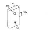
そこで、投影装置にカメラを搭載するようにしてもよい。この場合の投影装置5aの外観を図21に示し、投影装置5aの構成を図22に示す。
投影装置5aのマイクロコンピュータ501は、内部のメモリ(不図示)に格納されたプログラムに従って本実施例で説明する処理を実行し、レーザ制御部517と、位相制御部518と、カメラ519を制御するカメラ制御部520として機能する。
投影装置5aのマイクロコンピュータ501は、内部のメモリ(不図示)に格納されたプログラムに従って本実施例で説明する処理を実行し、レーザ制御部517と、位相制御部518と、カメラ519を制御するカメラ制御部520として機能する。
図14、図15から明らかなように、第1の実施例の投影装置5では、携帯端末6と有線接続する場合はUSBケーブルを使うことを想定している。このため、投影装置5のUSBコネクタ512はメス型のコネクタである。
一方、本実施例の投影装置5aの場合は、図23に示すようにオス型のUSBコネクタ512a(第1のコネクタ)を携帯端末6のUSBコネクタ603(第2のコネクタ)に差し込んで使用する。つまり、本実施例では、投影装置5aと携帯端末6との間の信号のやり取りは有線通信で行われる。
携帯端末6の構成は第1の実施例と同じである。
携帯端末6の構成は第1の実施例と同じである。
図24は本実施例の3次元計測方法を説明するフローチャートである。ユーザは、投影装置5aを携帯端末6に装着した後に、3次元計測用アプリケーションを起動して、投影装置5aのカメラ519を計測対象の物体に向ける。3次元計測用アプリケーションが起動すると、携帯端末6のカメラ制御部614は、カメラ起動制御信号を通信部610に渡す。通信部610は、カメラ起動制御信号を有線通信用の通信回路604に渡す。通信回路604は、カメラ起動制御信号を投影装置5aに送信する。
投影装置5aのカメラ制御部520は、USBコネクタ512aを介してカメラ起動制御信号を受信すると、カメラ519を起動して撮影可能な状態にする(図24ステップS100a)。
図24のステップS101,S102の処理は第1の実施例と同様である。携帯端末6の画像取得部608は、画像要求信号を通信部610に渡す。通信部610は、画像要求信号を通信回路604に渡す。通信回路604は、画像要求信号を投影装置5aに送信する。
投影装置5aのカメラ制御部520は、USBコネクタ512aを介して画像要求信号を受信すると、カメラ519によって撮影された物体の画像をUSBコネクタ512aを介して携帯端末6に送信する。
携帯端末6の画像取得部608は、投影装置5aから送信された画像を取得する(図24ステップS103a)。
携帯端末6の画像取得部608は、投影装置5aから送信された画像を取得する(図24ステップS103a)。
図24のステップS104,S106~S108の処理は第1の実施例と同様である。図24のステップS105aの処理はステップS103aと同じである。
こうして、本実施例では、投影装置5aの専用のカメラ519を用いて物体の3次元計測を行うことができる。本実施例では、出射口515の中心とカメラ519の受光面の中心との距離を一定にできる。したがって、高精度な3次元計測が可能である。
ただし、本実施例では、携帯端末6に標準的に搭載されているカメラ606とは別に、投影装置5aにカメラ519を搭載することになるため、コスト増になるというデメリットがある。
ただし、本実施例では、携帯端末6に標準的に搭載されているカメラ606とは別に、投影装置5aにカメラ519を搭載することになるため、コスト増になるというデメリットがある。
なお、製造時の寸法誤差は、事前の検査によって把握することができる。そこで、把握した誤差に基づく補正値を携帯端末6の画像解析部612のプログラムに設定しておくことにより誤差を補正することが可能である。
[第3の実施例]
第1、第2の実施例では、撮像した画像の解析を携帯端末6の画像解析部612によって行い、物体の3次元形状データを計算した。
これに対して、撮影した画像データや測定条件を専用のサーバー装置に送信し、サーバー装置によって物体の3次元形状データを計算し、計算結果を携帯端末6に送り返すようにしてもよい。
第1、第2の実施例では、撮像した画像の解析を携帯端末6の画像解析部612によって行い、物体の3次元形状データを計算した。
これに対して、撮影した画像データや測定条件を専用のサーバー装置に送信し、サーバー装置によって物体の3次元形状データを計算し、計算結果を携帯端末6に送り返すようにしてもよい。
本実施例のサーバー装置の構成を図25に示す。サーバー装置8は、CPU800と、メモリ801と、無線通信用の通信回路802とを備えている。CPU800は、メモリ801に格納されたプログラムに従って本実施例で説明する処理を実行し、通信部803と、画像解析部804として機能する。
投影装置5,5aと携帯端末6の構成は第1、第2の実施例と同じである。
投影装置5,5aと携帯端末6の構成は第1、第2の実施例と同じである。
図26は本実施例の3次元計測方法を説明するフローチャートである。図26のステップS100~S106の処理は第1の実施例と同様である。
携帯端末6の通信部615は、撮影された物体の画像データと測定条件情報(縞模様の位相情報など)とを通信回路607に渡す。通信回路607は、画像データと測定条件情報とをサーバー装置8に無線送信する(図26ステップS109)。
携帯端末6の通信部615は、撮影された物体の画像データと測定条件情報(縞模様の位相情報など)とを通信回路607に渡す。通信回路607は、画像データと測定条件情報とをサーバー装置8に無線送信する(図26ステップS109)。
サーバー装置8の通信部803は、通信回路802を介して携帯端末6から受信した画像データと測定条件情報とを画像解析部804に渡す(図26ステップS110)。
画像解析部804は、受信した画像を解析して、計測対象の物体の3次元形状データを計算する(図20ステップS111)。この画像解析部804の処理は、携帯端末6の画像解析部612の処理と同じである。
画像解析部804は、受信した画像を解析して、計測対象の物体の3次元形状データを計算する(図20ステップS111)。この画像解析部804の処理は、携帯端末6の画像解析部612の処理と同じである。
サーバー装置8の通信部803は、画像解析部804によって計算された3次元形状データを通信回路802に渡す。通信回路802は、3次元形状データを携帯端末6に送信する(図26ステップS112)。
携帯端末6の通信部615は、通信回路607を介してサーバー装置8から受信した3次元形状データを表示部613に渡す(図26ステップS113)。表示部613は、上記と同様に物体の画像を表示器605に表示させる(図26ステップS114)。
図26の説明では、第1の実施例に本実施例のサーバー装置8を適用する場合について説明しているが、第2の実施例にサーバー装置8を適用してもよいことは言うまでもない。
本実施例のようにサーバー装置8を用いる場合、携帯端末6とサーバー装置8との間の通信速度が十分に得られていれば、携帯端末6の処理を軽減することができ、携帯端末6の消費電力を低減することができる。その結果、携帯端末6の電池の消耗を抑えることができる。
また、本実施例では、投影装置5,5aと携帯端末6とによって取得した3次元形状データをサーバー装置8から別の端末に送ることが可能である。したがって、3次元形状データを別の端末と共有することが容易になるというメリットがある。
[第4の実施例]
次に、本発明の第4の実施例について説明する。第1~第3の実施例で説明したフリンジ生成部1においては、半導体レーザ2からなる光源と入力導波路102とY分岐導波路103と位相変調器106,107と出力導波路104,105とがほぼ直線上に配置されている。
次に、本発明の第4の実施例について説明する。第1~第3の実施例で説明したフリンジ生成部1においては、半導体レーザ2からなる光源と入力導波路102とY分岐導波路103と位相変調器106,107と出力導波路104,105とがほぼ直線上に配置されている。
このため、半導体レーザ2から出射光が、石英系光導波路からなる入力導波路102に結合する際に、モードフィールドの不整合から結合損失が発生する。第1の実施例の場合、結合損失は例えば約2.5dBであり、約半分弱の光が入力導波路102に結合せずに放射し、迷光となる。
第1~第3の実施例では、出力導波路104,105から出射した2光束の干渉により強度が空間的に正弦的に変調された縞模様が得られる。しかしながら、迷光が投影装置5,5aの出射口515に届き、出射口515から空間に放出されると、縞模様と迷光との予期せぬ干渉が発生し、物体の3次元形状データを計算する際の誤差が大きくなってしまう。
そこで、本実施例のフリンジ生成部1aは、図27に示すように、半導体レーザ2から入力導波路102への光の入射方向(図27のy方向)と出力導波路104,105からの光の出射方向(図27のx方向)とが交差するように、シリコン基板の面内で入力導波路102が曲がる構造となっている。
本実施例では、光導波路の比屈折率差を1%とし、入力導波路102の曲げ半径を1mmとして設計、製造した。フリンジ生成部1aの製造方法、半導体レーザ2との結合方法、フリンジ生成部1aと半導体レーザ2とをモジュール化する方法は、第1の実施例と同じである。
本実施例では、半導体レーザ2から入力導波路102への光の入射方向と出力導波路104,105からの光の出射方向とを交差させているため、半導体レーザ2からの出射光が石英系光導波路からなる入力導波路102に結合する際に、モードフィールドの不整合から結合損失として発生した迷光は、出力導波路104,105からはほとんど出射されない。そのため、投影装置から2光束が空間に放出された際に、正弦的に変調された縞模様を得ることができる。
本実施例においては、半導体レーザ2から入力導波路102への光の入射方向と出力導波路104,105からの光の出射方向とが直交するようにフリンジ生成部1aを作製した。石英系光導波路を含むチップの大きさによるが、半導体レーザ2から入力導波路102への光の入射方向に対する出力導波路104,105からの光の出射方向の傾きの角度θが概ね30度以上であれば、迷光が出力導波路104,105から出射することはなく、理想的に正弦的に変調された縞模様を得ることができる。
縞模様を発生させるために、光導波路を使う例は従来から提案されているが、いずれの例でも光ファイバーを使用している。
発明者は、2光束干渉により強度が空間的に正弦的に変調された縞模様を得る構成において、迷光が出力導波路の出射口から空間に放出されると、本来の縞模様に予期せぬ明暗が重なる結果が生じ、位相シフト法による3次元計測の精度が低下することをはじめて見出した。
発明者は、2光束干渉により強度が空間的に正弦的に変調された縞模様を得る構成において、迷光が出力導波路の出射口から空間に放出されると、本来の縞模様に予期せぬ明暗が重なる結果が生じ、位相シフト法による3次元計測の精度が低下することをはじめて見出した。
そして、発明者は、上記のように半導体レーザから入力導波路への光の入射方向と出力導波路からの光の出射方向とを交差させることにより、理想に近い正弦的に強度変化する縞模様が得られることをはじめて見出した。
本発明は、位相シフト法により物体の3次元形状を計測する技術に適用することができる。
1,1a…フリンジ生成部、2…半導体レーザ、3…サブキャリア、4…セラミック筐体、5,5a…投影装置、6…携帯端末、7…固定具、8…サーバー装置、100…シリコン基板、101…アンダークラッド、102…入力導波路、103…Y分岐導波路、104,105…出力導波路、106,107…位相変調器、108,109…ヒータ、110,112…ヒータパッド、111…グランドパッド、113…オーバークラッド、114…断熱溝、115…遮光溝、200…n型GaAs基板、201…n型AlGaInPクラッド、202…活性層、203…p型AlGaInPクラッド層、204…n型AlInPブロック層、205…n側電極、206…p側電極、300…シリコン基板、301…n側電極パッド、302…p側電極パッド、303…ワイヤ、400…45度プリズム、401,403,405,407,409…電極パッド、402,404,406,408,410…ワイヤ、411…蓋、412…ガラス、413…枠、414…レンズ、500…フリンジ生成光学モジュール、501…マイクロコンピュータ、502…通信モジュール、503…制御回路、504…DAコンバーター、505,506…トランジスタ、508…ボード、509…プリント基板、510…ピン、511…スルーホール、512,512a…USBコネクタ、513…電池、514…プラスチックケース、515…出射口、517…レーザ制御部、518…位相制御部、519,606…カメラ、520…カメラ制御部、600,800…CPU、601,801…メモリ、602,604,607,802…通信回路、603…USBコネクタ、605…表示器、606…カメラ、608…画像取得部、609…レーザ制御部、610,615,803…通信部、611…位相制御部、612,804…画像解析部、613…表示部、614…カメラ制御部、703…窓ガラス、704,705…目盛り、706…位置合わせ構造。
Claims (8)
- 2光束の干渉により縞模様を発生させて物体に投影するように構成された投影装置と、
携帯端末とを備え、
前記投影装置は、
位相変調器を含む平面光波回路からなり、前記縞模様を発生させるように構成されたフリンジ生成部と、
前記位相変調器を制御して前記縞模様の位相を変化させるように構成された位相制御部とを備え、
前記携帯端末は、
前記縞模様が投影された物体を撮影するように構成されたカメラと、
前記カメラによって撮影された、前記縞模様の位相が異なる複数枚の画像を解析して、前記物体の3次元形状データを計算するように構成された画像解析部とを備えることを特徴とする3次元計測システム。 - 請求項1記載の3次元計測システムにおいて、
前記フリンジ生成部は、
光源と、
前記光源の出力と結合する入力導波路と、
前記入力導波路に接続され光を2分岐させるように構成されたY分岐導波路と、
前記Y分岐導波路の出力に接続された2本の出力導波路と、
前記2本の出力導波路にそれぞれ設けられ、前記2本の出力導波路を伝搬する光の位相を変調するように構成された2つの前記位相変調器とを備えることを特徴とする3次元計測システム。 - 請求項2記載の3次元計測システムにおいて、
前記入力導波路は、前記光源から前記入力導波路への光の入射方向に対する前記出力導波路からの光の出射方向の傾きの角度が30度以上となるように中途で曲がることを特徴とする3次元計測システム。 - 請求項1乃至3のいずれか1項に記載の3次元計測システムにおいて、
前記携帯端末を挟み込むクリップ状の固定具をさらに備え、
前記投影装置は、前記固定具に固定され、
前記固定具は、前記投影装置の前記2光束の出射口と前記携帯端末のカメラとの相対位置を定めるための位置合わせ構造を備えることを特徴とする3次元計測システム。 - 請求項4記載の3次元計測システムにおいて、
前記位置合わせ構造は、
前記固定具が前記携帯端末に装着されたときに前記携帯端末のカメラの受光面を覆うように前記固定具に配設された透明板と、
前記透明板に形成された目盛りとから構成されることを特徴とする3次元計測システム。 - 2光束の干渉により縞模様を発生させて物体に投影するように構成された投影装置と、
携帯端末とを備え、
前記投影装置は、
位相変調器を含む平面光波回路からなり、前記縞模様を発生させるように構成されたフリンジ生成部と、
前記位相変調器を制御して前記縞模様の位相を変化させるように構成された位相制御部と、
前記縞模様が投影された物体を撮影するように構成されたカメラと、
前記カメラによって撮影された画像を前記携帯端末に送信するように構成された第1の通信部と、
前記携帯端末との通信用の第1のコネクタとを備え、
前記携帯端末は、
前記投影装置から画像を受信するように構成された第2の通信部と、
前記投影装置のカメラによって撮影された、前記縞模様の位相が異なる複数枚の画像を解析して、前記物体の3次元形状データを計算するように構成された画像解析部と、
前記投影装置との通信用の第2のコネクタとを備え、
前記投影装置は、前記第1のコネクタと前記第2のコネクタとが嵌合することにより、前記携帯端末に装着されることを特徴とする3次元計測システム。 - 請求項6記載の3次元計測システムにおいて、
前記フリンジ生成部は、
光源と、
前記光源の出力と結合する入力導波路と、
前記入力導波路に接続され光を2分岐させるように構成されたY分岐導波路と、
前記Y分岐導波路の出力に接続された2本の出力導波路と、
前記2本の出力導波路にそれぞれ設けられ、前記2本の出力導波路を伝搬する光の位相を変調するように構成された2つの前記位相変調器とを備えることを特徴とする3次元計測システム。 - 請求項7記載の3次元計測システムにおいて、
前記入力導波路は、前記光源から前記入力導波路への光の入射方向に対する前記出力導波路からの光の出射方向の傾きの角度が30度以上となるように中途で曲がることを特徴とする3次元計測システム。
Priority Applications (3)
| Application Number | Priority Date | Filing Date | Title |
|---|---|---|---|
| PCT/JP2020/018940 WO2021229675A1 (ja) | 2020-05-12 | 2020-05-12 | 3次元計測システム |
| JP2022522129A JP7424477B2 (ja) | 2020-05-12 | 2020-05-12 | 3次元計測システム |
| US17/996,016 US20230194248A1 (en) | 2020-05-12 | 2020-05-12 | Three-Dimensional Measurement System |
Applications Claiming Priority (1)
| Application Number | Priority Date | Filing Date | Title |
|---|---|---|---|
| PCT/JP2020/018940 WO2021229675A1 (ja) | 2020-05-12 | 2020-05-12 | 3次元計測システム |
Publications (1)
| Publication Number | Publication Date |
|---|---|
| WO2021229675A1 true WO2021229675A1 (ja) | 2021-11-18 |
Family
ID=78525486
Family Applications (1)
| Application Number | Title | Priority Date | Filing Date |
|---|---|---|---|
| PCT/JP2020/018940 Ceased WO2021229675A1 (ja) | 2020-05-12 | 2020-05-12 | 3次元計測システム |
Country Status (3)
| Country | Link |
|---|---|
| US (1) | US20230194248A1 (ja) |
| JP (1) | JP7424477B2 (ja) |
| WO (1) | WO2021229675A1 (ja) |
Families Citing this family (1)
| Publication number | Priority date | Publication date | Assignee | Title |
|---|---|---|---|---|
| CN116056621A (zh) * | 2020-08-05 | 2023-05-02 | 捷锐士阿希迈公司(以奥林巴斯美国外科技术名义) | 解剖目标的深度和轮廓检测 |
Citations (4)
| Publication number | Priority date | Publication date | Assignee | Title |
|---|---|---|---|---|
| JP2011106931A (ja) * | 2009-11-16 | 2011-06-02 | Roland Dg Corp | 3次元形状測定システムおよび携帯電話機 |
| JP2016106238A (ja) * | 2013-03-25 | 2016-06-16 | 技術研究組合光電子融合基盤技術研究所 | 光結合構造及び光モジュール |
| JP2016136237A (ja) * | 2015-01-20 | 2016-07-28 | 株式会社Cmサイト | 接写アダプタ |
| WO2018139510A1 (ja) * | 2017-01-25 | 2018-08-02 | オリンパス株式会社 | 位相変調器、位相変調器の制御方法および縞投影装置 |
Family Cites Families (16)
| Publication number | Priority date | Publication date | Assignee | Title |
|---|---|---|---|---|
| CA2044820C (en) * | 1990-06-19 | 1998-05-26 | Tsugito Maruyama | Three-dimensional measuring apparatus |
| US6816665B2 (en) * | 2002-05-09 | 2004-11-09 | Lynx Photonic Networks Inc. | Constant power operation thermo-optic switch |
| US7286246B2 (en) * | 2003-03-31 | 2007-10-23 | Mitutoyo Corporation | Method and apparatus for non-contact three-dimensional surface measurement |
| US8531650B2 (en) * | 2008-07-08 | 2013-09-10 | Chiaro Technologies LLC | Multiple channel locating |
| WO2012073483A1 (ja) * | 2010-11-29 | 2012-06-07 | 株式会社ニコン | マーク検出方法、露光方法及び露光装置、並びにデバイス製造方法 |
| WO2013036076A2 (ko) * | 2011-09-09 | 2013-03-14 | 주식회사 인스펙토 | 투영격자의 진폭을 적용한 3차원 형상 측정장치 및 방법 |
| US9448064B2 (en) * | 2012-05-24 | 2016-09-20 | Qualcomm Incorporated | Reception of affine-invariant spatial mask for active depth sensing |
| US8937657B2 (en) * | 2012-07-15 | 2015-01-20 | Erik Klass | Portable three-dimensional metrology with data displayed on the measured surface |
| US20140078264A1 (en) * | 2013-12-06 | 2014-03-20 | Iowa State University Research Foundation, Inc. | Absolute three-dimensional shape measurement using coded fringe patterns without phase unwrapping or projector calibration |
| WO2015183550A1 (en) * | 2014-05-27 | 2015-12-03 | Bourbaki 13, Inc. | Determining three-dimensional information from projections or placement of two-dimensional patterns |
| JP6524223B2 (ja) * | 2015-06-01 | 2019-06-05 | オリンパス株式会社 | 干渉縞投影装置及び計測装置 |
| CN109690240B (zh) * | 2016-06-20 | 2022-01-25 | 康耐视公司 | 用于将在时间上可变的光学图样投射到三维待测物体上的设备 |
| US10641934B2 (en) * | 2017-03-24 | 2020-05-05 | Rambus Inc. | Methods and systems for distinguishing point sources |
| JP6897398B2 (ja) * | 2017-07-31 | 2021-06-30 | セイコーエプソン株式会社 | 三次元形状測定装置、ロボットシステム、及び三次元形状測定方法 |
| US11336883B2 (en) * | 2019-07-23 | 2022-05-17 | Northwestern University | Method and system for three-dimensional surface measurement with a mobile device |
| JP7587460B2 (ja) * | 2021-04-02 | 2024-11-20 | 株式会社キーエンス | 三次元形状測定装置 |
-
2020
- 2020-05-12 US US17/996,016 patent/US20230194248A1/en not_active Abandoned
- 2020-05-12 WO PCT/JP2020/018940 patent/WO2021229675A1/ja not_active Ceased
- 2020-05-12 JP JP2022522129A patent/JP7424477B2/ja active Active
Patent Citations (4)
| Publication number | Priority date | Publication date | Assignee | Title |
|---|---|---|---|---|
| JP2011106931A (ja) * | 2009-11-16 | 2011-06-02 | Roland Dg Corp | 3次元形状測定システムおよび携帯電話機 |
| JP2016106238A (ja) * | 2013-03-25 | 2016-06-16 | 技術研究組合光電子融合基盤技術研究所 | 光結合構造及び光モジュール |
| JP2016136237A (ja) * | 2015-01-20 | 2016-07-28 | 株式会社Cmサイト | 接写アダプタ |
| WO2018139510A1 (ja) * | 2017-01-25 | 2018-08-02 | オリンパス株式会社 | 位相変調器、位相変調器の制御方法および縞投影装置 |
Also Published As
| Publication number | Publication date |
|---|---|
| US20230194248A1 (en) | 2023-06-22 |
| JPWO2021229675A1 (ja) | 2021-11-18 |
| JP7424477B2 (ja) | 2024-01-30 |
Similar Documents
| Publication | Publication Date | Title |
|---|---|---|
| JP5868488B2 (ja) | 座標計測装置及び三次元座標を計測する方法 | |
| Xu et al. | 3D-printed facet-attached microlenses for advanced photonic system assembly | |
| US11448836B2 (en) | Probe device and test device including the same comprising an optical fiber inserted into a hole of an intermediate substrate having a probe mirror | |
| JP5621861B2 (ja) | 光デバイス | |
| JP2001296449A (ja) | 角度が付けられた光学コネクタ | |
| JP2020526775A (ja) | フォトニック集積距離測定ピクセルおよび距離測定方法 | |
| CN105467585A (zh) | 光调制器以及图像显示装置 | |
| US20190339069A1 (en) | Optical measurement apparatus | |
| CN103563362A (zh) | 光学器件 | |
| JP7424477B2 (ja) | 3次元計測システム | |
| WO2012115133A1 (ja) | 光変調器 | |
| JP6435833B2 (ja) | 光モジュール | |
| KR102614185B1 (ko) | 폴리머 광ic 기반 레이저 집적형 이차원 빔스캐너 및 그의 제조 방법 | |
| KR20220110807A (ko) | 외부 광원으로부터의 광을 제어하기 위한 광학 장치 | |
| JP6331196B2 (ja) | 光学素子、照射光学系、集光光学系および光導波路検査装置 | |
| JP2020034862A (ja) | 光ファイバアレイおよび光学測定装置 | |
| JP6507659B2 (ja) | 光モジュールの製造方法 | |
| CN118355257A (zh) | 波导测量装置 | |
| JP4823584B2 (ja) | 光変調器 | |
| JP6089644B2 (ja) | 光素子接続方法及び光素子接続装置 | |
| Tyler et al. | Characterization of SiN integrated optical phased arrays on a wafer-scale test station | |
| KR102941204B1 (ko) | 레이저 측정 장치 | |
| CN110388884A (zh) | 结构光照明三维测量装置 | |
| TW200417763A (en) | Efficient coupling of light into light guides | |
| US20250285429A1 (en) | Method and system for imaging and image projection using integrated photonic components |
Legal Events
| Date | Code | Title | Description |
|---|---|---|---|
| 121 | Ep: the epo has been informed by wipo that ep was designated in this application |
Ref document number: 20935651 Country of ref document: EP Kind code of ref document: A1 |
|
| ENP | Entry into the national phase |
Ref document number: 2022522129 Country of ref document: JP Kind code of ref document: A |
|
| NENP | Non-entry into the national phase |
Ref country code: DE |
|
| 122 | Ep: pct application non-entry in european phase |
Ref document number: 20935651 Country of ref document: EP Kind code of ref document: A1 |