WO2021225031A1 - トランスコンダクタンス増幅器および受信装置 - Google Patents
トランスコンダクタンス増幅器および受信装置 Download PDFInfo
- Publication number
- WO2021225031A1 WO2021225031A1 PCT/JP2021/009750 JP2021009750W WO2021225031A1 WO 2021225031 A1 WO2021225031 A1 WO 2021225031A1 JP 2021009750 W JP2021009750 W JP 2021009750W WO 2021225031 A1 WO2021225031 A1 WO 2021225031A1
- Authority
- WO
- WIPO (PCT)
- Prior art keywords
- amplifier
- input
- auxiliary
- transconductance
- signal
- Prior art date
- Legal status (The legal status is an assumption and is not a legal conclusion. Google has not performed a legal analysis and makes no representation as to the accuracy of the status listed.)
- Ceased
Links
Images


Classifications
-
- H—ELECTRICITY
- H03—ELECTRONIC CIRCUITRY
- H03F—AMPLIFIERS
- H03F1/00—Details of amplifiers with only discharge tubes, only semiconductor devices or only unspecified devices as amplifying elements
- H03F1/02—Modifications of amplifiers to raise the efficiency, e.g. gliding Class A stages, use of an auxiliary oscillation
-
- H—ELECTRICITY
- H03—ELECTRONIC CIRCUITRY
- H03F—AMPLIFIERS
- H03F1/00—Details of amplifiers with only discharge tubes, only semiconductor devices or only unspecified devices as amplifying elements
- H03F1/26—Modifications of amplifiers to reduce influence of noise generated by amplifying elements
-
- H—ELECTRICITY
- H03—ELECTRONIC CIRCUITRY
- H03F—AMPLIFIERS
- H03F3/00—Amplifiers with only discharge tubes or only semiconductor devices as amplifying elements
- H03F3/34—DC amplifiers in which all stages are DC-coupled
-
- H—ELECTRICITY
- H04—ELECTRIC COMMUNICATION TECHNIQUE
- H04B—TRANSMISSION
- H04B1/00—Details of transmission systems, not covered by a single one of groups H04B3/00 - H04B13/00; Details of transmission systems not characterised by the medium used for transmission
- H04B1/06—Receivers
- H04B1/16—Circuits
- H04B1/18—Input circuits, e.g. for coupling to an antenna or a transmission line
Definitions
- This technology relates to a transconductance amplifier. More specifically, the present invention relates to a transconductance amplifier that converts an input voltage into an electric current, and a receiving device including the transconductance amplifier.
- Non-Patent Document 1 a technique for performing signal processing in a current mode using a transconductance amplifier is known (see, for example, Non-Patent Document 1).
- the dynamic range at a low power supply voltage is improved by utilizing the fact that the signal processing in the current mode is not easily restricted by the power supply voltage.
- the input impedance becomes resistant due to the feedback from the feedback amplifier, and while the input can be matched over a wide band, the noise of the feedback amplifier is directly input to the input of the amplifier, so that the noise figure deteriorates. There's a problem. Further, when the design is made to satisfy the input matching condition, there is a problem that the power consumption of the feedback amplifier is remarkably increased.
- This technology was created in view of this situation, and aims to reduce power consumption and noise in the transconductance amplifier.
- the first aspect thereof is a main amplifier that converts the voltage of an input signal into a current and outputs it, and is connected in parallel with the main amplifier.
- the auxiliary amplifier the feedback capacitance that inverts the phase of the output of the auxiliary amplifier and returns it to the input side, the gate capacitance that grounds the input of the auxiliary amplifier, the load capacitance that grounds the output of the auxiliary amplifier, and the above.
- It is a transconductance amplifier including an impedance matching circuit that matches the signal source impedance of an input signal with the input impedance of the auxiliary amplifier. This brings about the effect of reducing power consumption and noise by matching the impedance in the impedance matching circuit.
- a common mode feedback circuit that feeds back the output of the auxiliary amplifier to the inputs of the main amplifier and the auxiliary amplifier may be further provided. This has the effect of determining the DC potential of the output terminal.
- each of the main amplifier and the auxiliary amplifier may be provided with a thick film transistor that inputs the input signal to the gate. This has the effect of suppressing the effect of electrostatic discharge on the gate oxide film.
- each of the main amplifier and the auxiliary amplifier may be provided with a thin film transistor having a cascode configuration in the output unit. This has the effect of reducing the parasitic capacitance of the output section and improving the high frequency characteristics. In addition, the higher output impedance has the effect of improving the accuracy of the current output.
- a bias generation circuit for generating a bias voltage for the main amplifier and the auxiliary amplifier may be further provided. This has the effect of properly determining the bias voltage in each part of the main amplifier and the auxiliary amplifier.
- the impedance matching circuit may be an LC circuit having a series inductor and a shunt capacitance. This has the effect of matching the impedance with the LC circuit.
- the main amplifier may include a plurality of amplifiers connected in parallel.
- at least one of the plurality of amplifiers may be controlled to operate or not according to a predetermined control signal. This has the effect of combining the outputs of a plurality of amplifiers to make the gain variable as a whole.
- the gain of each of the plurality of amplifiers may be a predetermined fixed value, and in particular, the gain may be set to be twice or half that of the other amplifiers.
- the second aspect of the present technology is to convert the voltage of the received input signal into a current and output it, the auxiliary amplifier connected in parallel with the main amplifier, and the output phase of the auxiliary amplifier. Match the feedback capacitance that is inverted and fed back to the input side, the gate capacitance that grounds the input of the auxiliary amplifier, the load capacitance that grounds the output of the auxiliary amplifier, and the impedance of the input signal and the input of the auxiliary amplifier.
- a transconductance amplifier equipped with an impedance matching circuit, a current input mixer that multiplies the output current of the main amplifier by the output of the local oscillator to generate an intermediate frequency signal, and an interfering while amplifying the intermediate frequency signal to a predetermined level.
- An intermediate frequency processing unit that removes waves, an analog digital conversion unit that converts the amplified intermediate frequency signal from an analog value to a digital value, and a signal that performs predetermined signal processing on the intermediate frequency signal converted to the digital value. It is a receiving device including a processing unit. As a result, by using a transconductance amplifier whose impedance is matched in the impedance matching circuit, the power consumption and noise of the receiving device are reduced.
- a signal of a global satellite positioning system may be received as the above input signal.
- GNSS Global Navigation Satellite System
- Global satellite positioning systems require high gain, low noise, and low power consumption, but have a narrow signal band, which makes them useful as applications for the transconductance amplifier of the present technology.
- a plurality of the transconductance amplifiers that receive signals of different frequency bands as the input signals may be provided. This brings about the effect of simultaneously receiving signals of different frequency bands according to the setting of the value of each part of the transconductance amplifier.
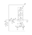
- FIG. 1 is a diagram showing a block configuration example of the transconductance amplifier 100 according to the embodiment of the present technology.
- the transconductance amplifier 100 includes a main amplifier 110, an auxiliary amplifier 120, a feedback capacitance 137, a gate capacitance 135, a load capacitance 136, a resistor 138, and an common mode feedback circuit 140. It is assumed that these are provided in the chip. An impedance matching circuit 180 is provided outside the chip.
- the main amplifier (Gm) 110 is an amplifier that converts the voltage of the input signal into a current and outputs it as an output current Iout.
- the auxiliary amplifier (Gmp) 120 is an amplifier that is branched into two from the input of the main amplifier 110 and connected in parallel.
- the gate width of the transistor of the auxiliary amplifier 120 is assumed to be, for example, about one tenth of that of the main amplifier 110. Therefore, the power consumption is about one tenth.
- the feedback capacitance (Cf) 137 is a capacitance that inverts the phase of the output of the auxiliary amplifier 120 and returns (negative feedback) to the input side.
- the gate capacitance (Cg) 135 is a capacitance that grounds the input of the auxiliary amplifier 120.
- the load capacity (Cl) 136 is a capacity for grounding the output of the auxiliary amplifier 120.
- the resistor (Rhigh) 138 is a resistor that connects the outputs of the main amplifier 110 and the auxiliary amplifier 120. The resistance value of this resistor 138 is large enough to be negligible in calculation.
- the common mode feedback circuit 140 is a common mode feedback (CMFB) circuit provided for determining the DC operating point of the outputs of the main amplifier 110 and the auxiliary amplifier 120.
- the capacitance (C6) 142 is a phase compensation capacitance for ensuring the stability of the common mode feedback loop.
- the input impedance of the common mode feedback circuit is assumed to be sufficiently high so that it can be ignored in calculation.
- the impedance matching circuit 180 is a circuit that matches the antenna impedance Rs (the signal source impedance of the input signal) with the input impedance of the auxiliary amplifier 120.
- the impedance matching circuit 180 includes a series inductor (Lm) 181 and a shunt capacitance (Cm) 182.
- a capacitor (Cdc) 193 for cutting a direct current (DC) component is provided on the input side of the impedance matching circuit 180.
- Voltage Vs is input to the transconductance amplifier 100 as an input signal. Further, here, assuming that the transconductance amplifier 100 is used in the receiving device, it is assumed that the antenna impedance Rs is, for example, 50 ⁇ .
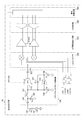
- FIG. 2 is a diagram showing a circuit configuration example of the transconductance amplifier 100 according to the embodiment of the present technology.
- the circuit configuration example shown here is basically the same as the block configuration described above. However, the bias generation circuit 150 and the electrostatic protection element 170 are not shown in the above-mentioned block configuration.
- the electrostatic protection element 170 is a circuit for protecting from a transient high voltage or high current due to electrostatic discharge (ESD: Electro-Static Discharge).
- the bias generation circuit 150 is a circuit that generates the bias voltage of the transistors of the main amplifier 110 and the auxiliary amplifier 120.
- the output of the auxiliary amplifier 120 is separated from the output of the main amplifier 110 in an alternating current (AC) by a high resistance (Rhigh) 138.
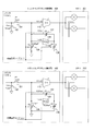
- FIG. 3 is a diagram showing a circuit configuration example of the main amplifier 110 according to the embodiment of the present technology.
- the main amplifier 110 has a configuration in which four transistors 111 to 114 are stacked in four stages.
- Transistors 111 and 114 are input transistors that receive input signals at the gate.
- HV high withstand voltage
- the bias voltages Vb1, Vb2 and Vb3 of the transistors 111, 112 and 113 are supplied from the bias generation circuit 150.
- the common mode feedback circuit 140 includes an operational amplifier 141, and feeds back the output of the main amplifier 110 to the input side of the main amplifier 110 via the resistor Rg1. Thereby, the DC potential of the output terminal is determined.
- FIG. 4 is a diagram showing a circuit configuration example of the auxiliary amplifier 120 according to the embodiment of the present technology.
- the auxiliary amplifier 120 has a configuration in which four transistors 121 to 124 are stacked in four stages.
- Transistors 121 and 124 are input transistors that receive input signals at the gate.
- Transistors 122 and 123 are output transistors that output current.
- the gate width of the transistors 121 to 124 is approximately one tenth of that of the transistors 111 to 114 of the main amplifier 110. This sets the bias current to one tenth of the main amplifier 110.
- the bias voltages Vb1, Vb2 and Vb3 of the transistors 121, 122 and 123 are common to the main amplifier 110 and are supplied from the bias generation circuit 150. Further, the common mode feedback circuit 140 that determines the DC potential of the output terminal is also shared with the main amplifier 110.
- the auxiliary amplifier 120 is loaded with a feedback capacity 137, a gate capacity 135, and a load capacity 136.
- the values of these capacitances may be variable.
- FIG. 5 is a diagram showing an example of a bias voltage generated by the bias generation circuit 150 in the embodiment of the present technology.
- This bias generation circuit 150 generates the optimum bias voltages Vb1, Vb2, Vb3 and Vref for an amplifier in which thick film transistors and thin film transistors coexist.
- the bias voltage Vb1 is supplied to the gates of the transistors 111 and 121.
- the bias voltage Vb2 is supplied to the gates of transistors 112 and 122.
- the bias voltage Vb3 is supplied to the gates of transistors 113 and 123.
- the bias voltage Vref is half the power supply voltage Vdd (Vdd / 2) and is supplied to the negative input terminal of the operational amplifier 141.
- the main amplifier 110 and the auxiliary amplifier 120 are mixed with thick-film transistors and thin film transistors stacked in four stages, but are suitable for obtaining stable characteristics even when the process, power supply voltage, and temperature fluctuate. It is necessary to apply the bias voltage. Since the variation between the thick film transistor and the thin film transistor is generally uncorrelated, it is desirable to be able to generate a bias voltage that appropriately follows the variation even when it varies independently.
- This bias generation circuit 150 is an example of realizing it.
- the transconductance amplifier 100 operates all MOSFETs in the subthreshold region.
- K is the aspect ratio (W / L) of the transistor.
- W is the gate width.
- L is the gate length.
- Vgs is the gate-source voltage.
- Vth is the threshold voltage.
- n is a subthreshold coefficient, and a typical value is about 1.7 to 1.8.
- ⁇ is the mobility.
- Cox is the gate oxide capacity.
- Vt is a thermal voltage, which is about 26 mV at room temperature of 300 K.
- the gate-source voltage Vgs is expressed by the following equation.
- Vgs n ⁇ Vt ⁇ ln (Id / (K ⁇ Is)) + Vth Therefore, the bias voltage Vb1 is given by the following equation.
- the subscript HV indicates that it is a high withstand voltage transistor.
- Vgs_MH6 n_HV ⁇ Vt ⁇ Ln ((I1 + I2) / (K_MH6 ⁇ Is_HV)) + Vth_HV
- Vgs_MH7 n_HV ⁇ Vt ⁇ ln (I2 / (K_MH7 ⁇ Is_HV)) + Vth_HV
- Vgs_MH6-Vgs_MH7 n_HV ⁇ Vt ⁇ Ln ((K_MH7 / K_MH6) (1+ (I1 / I2)))
- Vgs_ML6 n_LV ⁇ Vt ⁇ Ln (I1 / (K_ML6 ⁇ Is_LV)) + Vth_LV
- the subscript LV indicates that it is a thin film transistor.
- Vgs_MH9 n_HV ⁇ Vt ⁇ ln (I4 / (K_MH9 ⁇ Is_HV)) + Vth_HV
- Vgs_MH8 n_HV ⁇ Vt ⁇ Ln ((I4 + I5) / (K_MH8 ⁇ Is_HV)) + Vth_HV
- Vgs_ML8 n_HV ⁇ Vt ⁇ ln (I5 / (K_ML8 ⁇ Is_LV)) + Vth_LV
- the bias voltage Vref will be examined.
- the potential Vn at the connection point between the source of the transistor 156 (ML7) and the drain of the transistor 154 (ML6), and the connection point between the drain of the transistor 158 (ML8) and the source of the transistor 168 (ML9) can be expressed by the following equations.
- Vn (Vgs_MH6-Vgs_MH7) + (Vgs_ML6-Vgs_ML7)
- Vp Vdd- (Vgs_MH8-Vgs_MH9) -(Vgs_ML8-Vgs_ML9)
- Vref Vdd / 2
- bias voltages Vb1, Vb2, Vb3 and Vref By applying the bias voltages Vb1, Vb2, Vb3 and Vref in this way, stable characteristics can be obtained even when the process, power supply voltage and temperature fluctuate.
- Lm (Bp + (GpRs (Gp 2 + Bp 2 ) -Gp 2 ) 1/2 ) / ( ⁇ o (Gp 2 + Bp 2 ))
- Cm (GpRs (Gp 2 + Bp 2 ) -Gp 2 ) 1/2 / ⁇ oGpRs
- the mutual conductance Gmp of the auxiliary amplifier 120 is set to 1 mS, and the power consumption can be reduced. That is, since the auxiliary amplifier 120 does not directly generate 50 ⁇ , the power consumption is small.
- noise current of the auxiliary amplifier 120 of this embodiment goes out to the ground through the load capacitance 136. Also, peaking is applied by the impedance matching circuit 180. Therefore, the deterioration of the noise figure is small as compared with the conventional technique. Therefore, according to this embodiment, it can be seen that noise can be significantly reduced as compared with the prior art.
- the impedance matching circuit 180 since peaking is applied by the impedance matching circuit 180, it can be seen that even if an amplifier having the same transconductance (Gm) is used, the gain can be significantly improved as compared with the conventional technique.
- FIG. 6 is a diagram showing an example of a DC operating point of the transconductance amplifier 100 according to the embodiment of the present technology.
- This example shows an example in which the power supply voltage Vdd is set to 0.65V and an appropriate DC voltage is set for each part. As described above, it is assumed that each transistor stacked in four stages operates in the sub-threshold region.
- the transconductance amplifier 100 of the embodiment of the present technology includes an auxiliary amplifier 120 and an impedance matching circuit 180 which have been subjected to negative feedback by the feedback capacitance 137.
- the gain of the transconductance amplifier 100 can be improved, and power consumption and noise can be reduced.
- FIG. 7 is a diagram showing a block configuration example of the transconductance amplifier 100 in the first modification of the embodiment of the present technology.
- the transconductance amplifier 100 in this first modification divides the transconductance of the main amplifier 110 into 1: 2: 7, and is provided with a gain variable function of 0 dB, -10 dB, and -20 dB. That is, the amplifier 11 has a mutual conductance of Gm, the amplifier 12 has a mutual conductance of 2 Gm, and the amplifier 13 has a mutual conductance of 7 Gm.
- the output currents of the amplifiers 11 to 13 are added and output as the output current Iout.
- the presence or absence of operation of the amplifiers 12 and 13 is controlled by the control signals G0 and G1, respectively.
- FIG. 8 is a diagram showing an example of the relationship between the control signal and the gain of the transconductance amplifier 100 in the first modification of the embodiment of the present technology.
- G1 is “0” and G0 is “1”
- the amplifier 13 does not operate and the gain is 3 Gm ⁇ Q.
- the amplifier 12 does not operate and the gain is 8 Gm ⁇ Q.
- both G0 and G1 are "1”
- all the amplifiers 11 to 13 operate to reach 10 Gm ⁇ Q.
- the output level is based on the case where the gain is 10 Gm ⁇ Q (0 dB).
- the gain of the main amplifier 110 can be variably controlled. Even in this case, since the input impedance matching is performed by the auxiliary amplifier 120, changing the gain of the main amplifier 110 does not affect the impedance matching.
- FIG. 9 is a diagram showing a block configuration example of the transconductance amplifier 100 in the second modification of the embodiment of the present technology.
- the transconductance amplifier 100 in this second modification is obtained by dividing the mutual conductance of the main amplifier 110 by binary weighting, and has a finer gain resolution than the first modification described above.
- the gain Gain is given by the following equation.
- Gain (G0 + 2G1 + 2 2 G2 + ... + 2 N GN) ⁇ Gm ⁇ Q
- G0 to GN are gain control signals based on binary numbers of (N + 1) bits, and control the presence or absence of the corresponding amplifier operation as in the first modification described above.
- [G0 ... GN] [000 ... 0] to [111 ... 1]
- the gain of the main amplifier 110 can be variably controlled with a finer resolution.
- FIG. 10 is a diagram showing an example of a block configuration of a receiver in a third modification of the embodiment of the present technology.
- the receiver in this third modification shows an example of a GNSS receiver including the transconductance amplifier 100 of the above-described embodiment.
- a current input mixer 200, an intermediate frequency processing unit 300, an AD conversion unit 400, and a signal processing device 500 are connected to the subsequent stage of the transconductance amplifier 100.
- the signal (1720 MHz) from the LTE transmitter is close to the GPS transmission frequency (1575 MHz). Further, the transmission level from the LTE transmitter is about +25 dBm, which is higher than the GPS reception level of ⁇ 130 dBm. Therefore, the signal from the LTE transmitter can be a source of interference. In this respect, it is rather desirable that the band of the signal to be received in the GNSS receiver is narrow. Under such circumstances, it is suitable to use the transconductance amplifier 100, which can secure a wide dynamic range in the current mode operation, for the GNSS receiver.
- the current input mixer 200 multiplies the output current Iout of the transconductance amplifier 100 with the 4-phase oscillation frequency LO (Local Oscillator) to generate a low-frequency intermediate frequency (IF) signal.
- the intermediate frequency processing unit 300 includes an amplifier that amplifies the intermediate frequency signal to a predetermined level, and a filter that removes interfering waves.
- the AD conversion unit 400 converts the intermediate frequency signal processed by the intermediate frequency processing unit 300 into a digital signal.
- the signal processing device 500 uses the control signal RFAGC (Radio Frequency Automatic Gain Control) or IFAGC (Intermediate Frequency Automatic Gain Control) according to the reception level of the digital intermediate frequency signal to obtain the gain Gm of the main amplifier 110 and the intermediate frequency processing unit 300. Controls the gain of the amplifier. That is, when the reception level is higher than a predetermined threshold value, the gain of the main amplifier 110 is made relatively small. On the other hand, when the reception level is lower than the predetermined threshold value, the gain of the main amplifier 110 is relatively increased.
- the control signal RFAGC in this case can be handled according to the control signal of the first or second modification described above.
- the GNSS receiver can be configured by using the transconductance amplifier 100 of the above-described embodiment.
- the gain of the main amplifier 110 can be variably controlled by using the control signal of the first or second modification described above.
- FIG. 11 is a diagram showing a block configuration example of the transconductance amplifiers 101 and 102 in the fourth modification of the embodiment of the present technology.
- This receiver is a device that receives signals in the L1 (1.6 GHz) frequency band and the L5 (1.2 GHz) frequency band.
- the outputs of the transconductance amplifiers 101 and 102 are supplied to the current input mixers 201 and 202, respectively.
- the processing procedure described in the above-described embodiment may be regarded as a method having these series of procedures, or as a program for causing a computer to execute these series of procedures or as a recording medium for storing the program. You may catch it.
- this recording medium for example, a CD (Compact Disc), MD (MiniDisc), DVD (Digital Versatile Disc), memory card, Blu-ray Disc (Blu-ray (registered trademark) Disc) and the like can be used.
- the present technology can have the following configurations.
- a main amplifier that converts the voltage of the input signal into a current and outputs it.
- An auxiliary amplifier connected in parallel with the main amplifier, The feedback capacitance that inverts the phase of the output of the auxiliary amplifier and feeds it back to the input side, The gate capacitance for grounding the input of the auxiliary amplifier and The load capacity for grounding the output of the auxiliary amplifier and
- a transconductance amplifier including an impedance matching circuit that matches the signal source impedance of the input signal with the input impedance of the auxiliary amplifier.
- each of the main amplifier and the auxiliary amplifier includes a thick film transistor that inputs the input signal to the gate.
- each of the main amplifier and the auxiliary amplifier includes a thin film transistor having a cascode configuration in an output unit.
- the impedance matching circuit is an LC circuit including a series inductor and a shunt capacitance.
- the main amplifier that converts the voltage of the received input signal into a current and outputs it, the auxiliary amplifier connected in parallel with the main amplifier, and the output phase of the auxiliary amplifier are inverted and fed back to the input side.
- Transconductance including a feedback capacitance, a gate capacitance that grounds the input of the auxiliary amplifier, a load capacitance that grounds the output of the auxiliary amplifier, and an impedance matching circuit that matches the impedance of the input signal and the input of the auxiliary amplifier.
- a current input mixer that generates an intermediate frequency signal by multiplying the output current of the main amplifier and the output of the local oscillator.
- An intermediate frequency processing unit that amplifies the intermediate frequency signal to a predetermined level and removes interfering waves.
- An analog-to-digital converter that converts the amplified intermediate frequency signal from an analog value to a digital value
- a receiving device including a signal processing unit that performs predetermined signal processing on an intermediate frequency signal converted into a digital value. (12) The receiving device according to (11) above, which receives a signal of a global satellite positioning system as the input signal. (13) The receiving device according to (11) or (12), further comprising the plurality of transconductance amplifiers that receive signals in different frequency bands as the input signals.
Landscapes
- Engineering & Computer Science (AREA)
- Power Engineering (AREA)
- Computer Networks & Wireless Communication (AREA)
- Signal Processing (AREA)
- Amplifiers (AREA)
Priority Applications (1)
| Application Number | Priority Date | Filing Date | Title |
|---|---|---|---|
| JP2022519901A JPWO2021225031A1 (https=) | 2020-05-08 | 2021-03-11 |
Applications Claiming Priority (2)
| Application Number | Priority Date | Filing Date | Title |
|---|---|---|---|
| JP2020082305 | 2020-05-08 | ||
| JP2020-082305 | 2020-05-08 |
Publications (1)
| Publication Number | Publication Date |
|---|---|
| WO2021225031A1 true WO2021225031A1 (ja) | 2021-11-11 |
Family
ID=78468008
Family Applications (1)
| Application Number | Title | Priority Date | Filing Date |
|---|---|---|---|
| PCT/JP2021/009750 Ceased WO2021225031A1 (ja) | 2020-05-08 | 2021-03-11 | トランスコンダクタンス増幅器および受信装置 |
Country Status (2)
| Country | Link |
|---|---|
| JP (1) | JPWO2021225031A1 (https=) |
| WO (1) | WO2021225031A1 (https=) |
Cited By (2)
| Publication number | Priority date | Publication date | Assignee | Title |
|---|---|---|---|---|
| CN114567266A (zh) * | 2022-04-28 | 2022-05-31 | 成都嘉纳海威科技有限责任公司 | 一种低功耗低噪声宽带放大器 |
| WO2025239026A1 (ja) * | 2024-05-17 | 2025-11-20 | ソニーセミコンダクタソリューションズ株式会社 | 増幅装置およびバラン |
Citations (2)
| Publication number | Priority date | Publication date | Assignee | Title |
|---|---|---|---|---|
| JP2001267853A (ja) * | 2000-02-29 | 2001-09-28 | Lucent Technol Inc | フィードフォワード補償負帰還回路 |
| JP2008295060A (ja) * | 2007-05-17 | 2008-12-04 | Natl Semiconductor Corp <Ns> | 自動ゼロ化電流フィードバックインスツルメンテーションアンプ |
Family Cites Families (8)
| Publication number | Priority date | Publication date | Assignee | Title |
|---|---|---|---|---|
| GB9219685D0 (en) * | 1992-09-17 | 1992-10-28 | Massachusetts Inst Technology | Error reduction |
| US6208206B1 (en) * | 1999-02-11 | 2001-03-27 | The Hong Kong University Of Science And Technology | Frequency compensation techniques for low-power multistage amplifiers |
| JP4354465B2 (ja) * | 2006-03-24 | 2009-10-28 | シャープ株式会社 | 可変利得増幅器及びこの可変利得増幅器を備えた通信装置 |
| US7876146B2 (en) * | 2007-05-08 | 2011-01-25 | Qualcomm, Incorporated | Method and apparatus for powering down analog integrated circuits |
| US8102206B2 (en) * | 2009-05-08 | 2012-01-24 | Analog Devices, Inc. | Multi-path, multi-stage feed-forward operational amplifier circuit |
| JP4937366B2 (ja) * | 2010-03-05 | 2012-05-23 | 株式会社東芝 | 増幅器、及び通信装置 |
| US8725105B2 (en) * | 2012-05-24 | 2014-05-13 | Mediatek Inc. | Low noise amplifier and saw-less receiver with low-noise amplifier |
| US8963639B2 (en) * | 2013-02-19 | 2015-02-24 | University Of Macau | Frequency compensation techniques for low-power and small-area multistage amplifiers |
-
2021
- 2021-03-11 JP JP2022519901A patent/JPWO2021225031A1/ja active Pending
- 2021-03-11 WO PCT/JP2021/009750 patent/WO2021225031A1/ja not_active Ceased
Patent Citations (2)
| Publication number | Priority date | Publication date | Assignee | Title |
|---|---|---|---|---|
| JP2001267853A (ja) * | 2000-02-29 | 2001-09-28 | Lucent Technol Inc | フィードフォワード補償負帰還回路 |
| JP2008295060A (ja) * | 2007-05-17 | 2008-12-04 | Natl Semiconductor Corp <Ns> | 自動ゼロ化電流フィードバックインスツルメンテーションアンプ |
Cited By (2)
| Publication number | Priority date | Publication date | Assignee | Title |
|---|---|---|---|---|
| CN114567266A (zh) * | 2022-04-28 | 2022-05-31 | 成都嘉纳海威科技有限责任公司 | 一种低功耗低噪声宽带放大器 |
| WO2025239026A1 (ja) * | 2024-05-17 | 2025-11-20 | ソニーセミコンダクタソリューションズ株式会社 | 増幅装置およびバラン |
Also Published As
| Publication number | Publication date |
|---|---|
| JPWO2021225031A1 (https=) | 2021-11-11 |
Similar Documents
| Publication | Publication Date | Title |
|---|---|---|
| US8310312B2 (en) | Amplifiers with improved linearity and noise performance | |
| KR101115266B1 (ko) | 능동 포스트-왜곡 선형화된 차동 증폭기 | |
| CN101904091B (zh) | 低噪声和低输入电容的差动修正型导数叠加低噪声放大器 | |
| CN103534940B (zh) | 正反馈共栅极低噪声放大器 | |
| EP1911154B1 (en) | Amplifier with active post-distortion linearization | |
| US7884673B2 (en) | Wideband low-noise amplifier | |
| US9806677B2 (en) | Amplifier adapted for noise suppression | |
| WO2021225031A1 (ja) | トランスコンダクタンス増幅器および受信装置 | |
| US9755680B2 (en) | Circuits for field-programmable receiver front ends | |
| US20080252377A1 (en) | Low noise amplifier having improved linearity | |
| US8823452B2 (en) | GM-ratioed amplifier | |
| US9413300B2 (en) | Front-end matching amplifier | |
| CN116566332A (zh) | 一种低功耗宽带低噪声放大器 | |
| JP2008118321A (ja) | 増幅器 | |
| US9935587B2 (en) | High linearity inductorless LNA | |
| US20220393655A1 (en) | Linearization using complementary devices | |
| US11437965B2 (en) | Variable gain amplifier and wireless communication device | |
| Kim et al. | A 0.018-mm 2 0.05-2 GHz Balun-LNA With Post-Linearization and Balanced Loads Achieving 33.5-dBm OIP3 and 3.7-dB NF | |
| Li et al. | A 23–40 GHz Compact LNA with Dual-Path Noise-Cancelling Technology Enabled by a Quad-Coil Coupled Transformer | |
| CN220798224U (zh) | 共源共栅放大电路、雷达设备、雷达系统及电子设备 | |
| KR102449479B1 (ko) | 전력 증폭기 | |
| Shumail et al. | Fully integrated, highly linear, wideband LNA in 0.13 μm CMOS technology | |
| Nanditha et al. | Design of a 2.4 GHz Low Noise Amplifier | |
| Raihan et al. | A 2.4 GHz gain-boosted CMOS amplifier using multibias points for improved linearization | |
| Usharani et al. | A high linearity low noise amplifier with modified differential inductor for bluetooth profiles. |
Legal Events
| Date | Code | Title | Description |
|---|---|---|---|
| 121 | Ep: the epo has been informed by wipo that ep was designated in this application |
Ref document number: 21800258 Country of ref document: EP Kind code of ref document: A1 |
|
| ENP | Entry into the national phase |
Ref document number: 2022519901 Country of ref document: JP Kind code of ref document: A |
|
| NENP | Non-entry into the national phase |
Ref country code: DE |
|
| 122 | Ep: pct application non-entry in european phase |
Ref document number: 21800258 Country of ref document: EP Kind code of ref document: A1 |