JP4937366B2 - 増幅器、及び通信装置 - Google Patents
増幅器、及び通信装置 Download PDFInfo
- Publication number
- JP4937366B2 JP4937366B2 JP2010049550A JP2010049550A JP4937366B2 JP 4937366 B2 JP4937366 B2 JP 4937366B2 JP 2010049550 A JP2010049550 A JP 2010049550A JP 2010049550 A JP2010049550 A JP 2010049550A JP 4937366 B2 JP4937366 B2 JP 4937366B2
- Authority
- JP
- Japan
- Prior art keywords
- signal
- phase
- positive
- amplifier
- negative
- Prior art date
- Legal status (The legal status is an assumption and is not a legal conclusion. Google has not performed a legal analysis and makes no representation as to the accuracy of the status listed.)
- Expired - Fee Related
Links
Images


Classifications
-
- G—PHYSICS
- G06—COMPUTING OR CALCULATING; COUNTING
- G06F—ELECTRIC DIGITAL DATA PROCESSING
- G06F3/00—Input arrangements for transferring data to be processed into a form capable of being handled by the computer; Output arrangements for transferring data from processing unit to output unit, e.g. interface arrangements
- G06F3/01—Input arrangements or combined input and output arrangements for interaction between user and computer
- G06F3/03—Arrangements for converting the position or the displacement of a member into a coded form
- G06F3/033—Pointing devices displaced or positioned by the user, e.g. mice, trackballs, pens or joysticks; Accessories therefor
-
- H—ELECTRICITY
- H03—ELECTRONIC CIRCUITRY
- H03F—AMPLIFIERS
- H03F3/00—Amplifiers with only discharge tubes or only semiconductor devices as amplifying elements
- H03F3/20—Power amplifiers, e.g. Class B amplifiers, Class C amplifiers
- H03F3/21—Power amplifiers, e.g. Class B amplifiers, Class C amplifiers with semiconductor devices only
- H03F3/211—Power amplifiers, e.g. Class B amplifiers, Class C amplifiers with semiconductor devices only using a combination of several amplifiers
-
- H—ELECTRICITY
- H03—ELECTRONIC CIRCUITRY
- H03F—AMPLIFIERS
- H03F3/00—Amplifiers with only discharge tubes or only semiconductor devices as amplifying elements
- H03F3/45—Differential amplifiers
-
- H—ELECTRICITY
- H03—ELECTRONIC CIRCUITRY
- H03F—AMPLIFIERS
- H03F3/00—Amplifiers with only discharge tubes or only semiconductor devices as amplifying elements
- H03F3/45—Differential amplifiers
- H03F3/45071—Differential amplifiers with semiconductor devices only
- H03F3/45076—Differential amplifiers with semiconductor devices only characterised by the way of implementation of the active amplifying circuit in the differential amplifier
- H03F3/45475—Differential amplifiers with semiconductor devices only characterised by the way of implementation of the active amplifying circuit in the differential amplifier using IC blocks as the active amplifying circuit
-
- H—ELECTRICITY
- H03—ELECTRONIC CIRCUITRY
- H03F—AMPLIFIERS
- H03F3/00—Amplifiers with only discharge tubes or only semiconductor devices as amplifying elements
- H03F3/68—Combinations of amplifiers, e.g. multi-channel amplifiers for stereophonics
Landscapes
- Engineering & Computer Science (AREA)
- Power Engineering (AREA)
- General Engineering & Computer Science (AREA)
- Theoretical Computer Science (AREA)
- Human Computer Interaction (AREA)
- Physics & Mathematics (AREA)
- General Physics & Mathematics (AREA)
- Amplifiers (AREA)
- Control Of Amplification And Gain Control (AREA)
Description
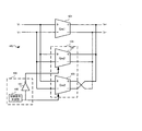
図1は、本発明の第1の実施形態に係る増幅器100を示す図である。本実施形態に係る増幅器100は、正相入力信号を増幅して正相出力信号を生成し、逆相入力信号を増幅して逆相出力信号を生成する。増幅器100は、正相入力信号を増幅して第1正相信号を生成し、逆相入力信号を増幅して第1逆相信号を生成する第1増幅回路101を有している。また増幅器100は、正相入力信号を増幅して第2正相信号を生成し、逆相入力信号を増幅して第2逆相信号を生成する第1増幅部102と、正相入力信号を増幅して第3正相信号を生成し、逆相入力信号を増幅して第3逆相信号を生成する第2増幅部103とを有する第2増幅回路104を備えている。

図6を用いて本実施形態に係る増幅器300を説明する。本実施形態に係る増幅器300は、第2増幅回路304、制御部305の構成及び動作が図1の増幅器100と異なる。図6に示すように、制御部305は、制御信号を生成し第2増幅回路304に出力する。
図8を用いて本実施形態に係る増幅器400を説明する。本実施形態に係る増幅器400は、第2増幅回路404の構成及び動作が図6の増幅器300と異なる。
図10を用いて本実施形態に係る増幅器500を説明する。本実施形態に係る増幅器500は、第3乃至第n増幅回路503〜50n(nは3以上の整数)を有している点が図1の増幅器100と異なる。
増幅器500が、第1増幅回路101、第2増幅回路104、第3増幅回路503を有するとする。この時、例えば、第1増幅回路101のトランスコンダクタンス値gm1が、第3増幅回路503が有する第1−3,2−3増幅部102−3,103−3のトランスコンダクタンス値gm3の5倍(gm1=5*gm3)であるとする。また第2増幅回路104が有する第1,2増幅部102,103のトランスコンダクタンス値gm2が、第3増幅回路503が有する第1−3,2−3増幅部102−3,103−3のトランスコンダクタンス値gm3の2倍(gm1=2*gm3)であるとする。
また、n>3であってもよい。例えば、n=4の場合、第1増幅回路101のトランスコンダクタンス値gm1、第2増幅回路104が有する第1,2増幅部102,103のトランスコンダクタンス値gm2、第3増幅回路503が有する第1−3,2−3増幅部102−3,103−3のトランスコンダクタンス値gm3、第4増幅回路504が有する第1−4,2−4増幅部102−4,103−4のトランスコンダクタンス値gm4の比を、gm1:gm2:gm3:gm4=9:4:2:1とする。この場合、増幅器500の利得を、利得の最低値を0dBに規格化して、0dB,6dB,12dB,18dBと可変にすることができる。またn=4の別の例として、gm1:gm2:gm3:gm4=45:6:5:4としてもよい。この場合、この場合増幅器500の利得を、利得の最低値を0dBに規格化して、0dB,2dB,4dB,6dBと可変にすることができる。
n=7の場合、第1〜7増幅回路のトランスコンダクタンス値をそれぞれgm1〜gm7とする。なお、第2〜7増幅回路のトランスコンダクタンス値とは、第2〜7増幅回路が有する各増幅部が有するトランスコンダクタンス値とする。第1〜7増幅回路のトランスコンダクタンス値の比を、gm1:gm2:gm3:gm4:gm5:gm6:gm7=45:3:3:3:2:2:2とする。この場合、増幅器500の利得を、利得の最低値を0dBに規格化して、0dB,1dB,2dB,3dB,4dB,5dB,6dBと可変にすることができる。
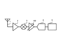
図11を用いて本発明の第5実施形態を説明する。図11は、本実施形態に係る通信装置は、アンテナ1と、低雑音増幅器2と、ミキサ3と、図1に示す増幅器100と、A/D変換器4と、信号処理部5とを有している。
Claims (10)
- 正相入力信号を増幅して正相出力信号を生成し、逆相入力信号を増幅して逆相出力信号を生成する増幅器であって、
前記正相入力信号を増幅して第1正相信号を生成し、前記逆相入力信号を増幅して第1逆相信号を生成する第1増幅回路と、
前記正相入力信号を増幅して第2正相信号を生成し、前記逆相入力信号を増幅して第2逆相信号を生成する第1増幅部と、前記正相入力信号を増幅して第3正相信号を生成し、前記逆相入力信号を増幅して第3逆相信号を生成する第2増幅部とを有する第2増幅回路と、を備え、
前記正相出力信号が前記第1正相信号と前記第2正相信号との和であって、かつ前記逆相出力信号が前記第1逆相信号と前記第2逆相信号との和であるか、
又は、前記正相出力信号が前記第1正相信号と前記第3逆相信号の和であって、かつ前記逆相出力信号が前記第1逆相信号と前記第3正相信号との和であることを特徴とする増幅器。 - 前記第1増幅部又は前記第2増幅部の一方をオンとし他方をオフとすることを特徴とする請求項1記載の増幅器。
- 前記第1増幅部及び前記第2増幅部のトランスコンダクタンス値が同じであることを特徴とする請求項1記載の増幅器。
- 前記第1増幅部及び前記第2増幅部の出力抵抗値が同じであることを特徴とする請求項1記載の増幅器。
- 前記第1増幅部は、第1トランジスタ対と第1電流源と、を有し、
前記第2増幅部は、第2トランジスタ対と第2電流源と、を有し、
前記第1電流源及び前記第2電流源の一方がオンとされ他方がオフとされることを特徴とする請求項1記載の増幅器。 - 前記第2増幅回路は、第1トランジスタ対と、第2トランジスタ対と、前記第1トランジスタ対又は前記第2トランジスタ対の一方に電流を供給する電流源と、を備え、
前記第1増幅部は、前記第1トランジスタ対と電流源とを有し、
前記第2増幅部は、前記第2トランジスタ対と電流源とを有することを特徴とする請求項1記載の増幅器。 - 前記第2増幅回路は、第3トランジスタ対をさらに備え、
前記第1増幅部は、前記第1トランジスタ対と、電流源と、前記第3トランジスタ対とを有し、
前記第2増幅部は、前記第2トランジスタ対と、電流源と、前記第3トランジスタ対とを有することを特徴とする請求項5記載の増幅器。 - 前記第2増幅回路は、前記第1トランジスタ対又は前記第2トランジスタ対の一方にバイアス電圧を印加することで、前記第2正相/逆相信号又は前記第3正相/逆相信号の一方を生成することを特徴とする請求項6記載の増幅器。
- 正相入力信号を増幅して正相出力信号を生成し、逆相入力信号を増幅して逆相出力信号を生成する増幅器であって、
前記正相入力信号を増幅して第1正相信号を生成し、前記逆相入力信号を増幅して第1逆相信号を生成する第1増幅回路と、
前記正相入力信号を増幅して第2正相信号を生成し、前記逆相入力信号を増幅して第2逆相信号を生成する第1増幅部と、前記正相入力信号を増幅して第3正相信号を生成し、前記逆相入力信号を増幅して第3逆相信号を生成する第2増幅部とを有する第2増幅回路と、
前記正相入力信号を増幅して第4正相信号を生成し、前記逆相入力信号を増幅して第4逆相信号を生成する第3増幅部と、前記正相入力信号を増幅して第5正相信号を生成し、前記逆相入力信号を増幅して第5逆相信号を生成する第4増幅部とを有する第3増幅回路と、を備え、
前記正相出力信号が前記第1正相信号と前記第2正相信号と前記第4正相信号との和であって、かつ前記逆相出力信号が前記第1逆相信号と前記第2逆相信号と前記第4逆相信号との和であるか、
又は、前記正相出力信号が前記第1正相信号と前記第3逆相信号と前記第4正相信号との和であって、かつ前記逆相出力信号が前記第1逆相信号と前記第3正相信号と前記第4逆相信号との和であるか、
又は、前記正相出力信号が前記第1正相信号と前記第3逆相信号と前記第5逆相信号との和であって、かつ前記逆相出力信号が前記第1逆相信号と前記第3正相信号と前記第5正相信号との和であることを特徴とする増幅器。 - 無線信号を受信するアンテナと、
前記無線信号を増幅する請求項1の増幅器と、
前記無線信号に信号処理を施し、受信信号を生成する受信部と、
を備えることを特徴とする通信装置。
Priority Applications (2)
| Application Number | Priority Date | Filing Date | Title |
|---|---|---|---|
| JP2010049550A JP4937366B2 (ja) | 2010-03-05 | 2010-03-05 | 増幅器、及び通信装置 |
| US12/877,497 US8331875B2 (en) | 2010-03-05 | 2010-09-08 | Amplifier and communication apparatus |
Applications Claiming Priority (1)
| Application Number | Priority Date | Filing Date | Title |
|---|---|---|---|
| JP2010049550A JP4937366B2 (ja) | 2010-03-05 | 2010-03-05 | 増幅器、及び通信装置 |
Publications (3)
| Publication Number | Publication Date |
|---|---|
| JP2011188117A JP2011188117A (ja) | 2011-09-22 |
| JP2011188117A5 JP2011188117A5 (ja) | 2011-11-04 |
| JP4937366B2 true JP4937366B2 (ja) | 2012-05-23 |
Family
ID=44531759
Family Applications (1)
| Application Number | Title | Priority Date | Filing Date |
|---|---|---|---|
| JP2010049550A Expired - Fee Related JP4937366B2 (ja) | 2010-03-05 | 2010-03-05 | 増幅器、及び通信装置 |
Country Status (2)
| Country | Link |
|---|---|
| US (1) | US8331875B2 (ja) |
| JP (1) | JP4937366B2 (ja) |
Families Citing this family (4)
| Publication number | Priority date | Publication date | Assignee | Title |
|---|---|---|---|---|
| US9225565B2 (en) | 2012-03-20 | 2015-12-29 | Intel Deutschland Gmbh | Device for generating a vector-modulated output signal and method for generating a vector-modulated output signal |
| KR102506436B1 (ko) * | 2015-11-30 | 2023-03-07 | 삼성전자주식회사 | 증폭 회로에서 입력 신호를 복원하는 방법 및 이를 이용하는 증폭 회로 |
| JP2019115009A (ja) * | 2017-12-26 | 2019-07-11 | アズビル株式会社 | 入力回路 |
| WO2021225031A1 (ja) * | 2020-05-08 | 2021-11-11 | ソニーセミコンダクタソリューションズ株式会社 | トランスコンダクタンス増幅器および受信装置 |
Family Cites Families (10)
| Publication number | Priority date | Publication date | Assignee | Title |
|---|---|---|---|---|
| JPH03214463A (ja) | 1990-01-19 | 1991-09-19 | Mitsubishi Electric Corp | 磁気ディスクシステム |
| EP0690561B1 (en) * | 1994-06-30 | 2001-10-31 | STMicroelectronics S.r.l. | Method for erasing a common mode current signal and transconductor assembly using such method |
| KR960027254A (ko) * | 1994-12-29 | 1996-07-22 | 조백제 | 선형성이 양호한 오퍼레이션널 트랜스콘덕턴스 증폭기 |
| JPH11330876A (ja) * | 1998-05-15 | 1999-11-30 | Nec Corp | 電圧制御増幅回路 |
| US6188281B1 (en) * | 1998-09-30 | 2001-02-13 | Maxim Integrated Products, Inc. | Linear transconductance circuits having class AB amplifiers parallel coupled with concave compensation circuits |
| JP3214463B2 (ja) | 1998-10-21 | 2001-10-02 | 日本電気株式会社 | 無線通信装置 |
| JP4682419B2 (ja) * | 2000-12-22 | 2011-05-11 | 日本テキサス・インスツルメンツ株式会社 | 可変利得増幅回路 |
| JP2007043289A (ja) * | 2005-08-01 | 2007-02-15 | Toshiba Corp | 増幅回路とこれを用いたフィルタ及び無線通信装置 |
| US7250813B1 (en) * | 2005-10-21 | 2007-07-31 | National Semiconductor Corporation | Split amplifier architecture for cross talk cancellation |
| JP2007258956A (ja) * | 2006-03-22 | 2007-10-04 | Nec Electronics Corp | 信号増幅回路および光受信器 |
-
2010
- 2010-03-05 JP JP2010049550A patent/JP4937366B2/ja not_active Expired - Fee Related
- 2010-09-08 US US12/877,497 patent/US8331875B2/en not_active Expired - Fee Related
Also Published As
| Publication number | Publication date |
|---|---|
| JP2011188117A (ja) | 2011-09-22 |
| US8331875B2 (en) | 2012-12-11 |
| US20110217941A1 (en) | 2011-09-08 |
Similar Documents
| Publication | Publication Date | Title |
|---|---|---|
| US8258869B2 (en) | Low noise amplifier with current bleeding branch | |
| US6882226B2 (en) | Broadband variable gain amplifier with high linearity and variable gain characteristic | |
| JP4468422B2 (ja) | カーテシアンループを用いた無線送信装置 | |
| JP5045151B2 (ja) | 送信電力制御回路 | |
| US8102209B2 (en) | CMOS variable gain amplifier | |
| US7193466B2 (en) | Operational transconductance amplifier with DC offset elimination and low mismatch | |
| US8711024B2 (en) | Switched capacitor amplifier | |
| US8725105B2 (en) | Low noise amplifier and saw-less receiver with low-noise amplifier | |
| US7538605B2 (en) | Amplifier device capable of reducing offset voltage | |
| US6650883B1 (en) | Mixer with adjustable linearity | |
| US7372330B2 (en) | Variable gain amplifier | |
| JP4937366B2 (ja) | 増幅器、及び通信装置 | |
| KR101127461B1 (ko) | 고도의 선형 가변이득 증폭기 | |
| US20090261903A1 (en) | Variable gain rf amplifier | |
| US20110090010A1 (en) | Variable gain amplification device | |
| US9746862B2 (en) | Voltage-to-current converter | |
| US20060217101A1 (en) | Higher linearity passive mixer | |
| JP4444174B2 (ja) | 周波数変換器及び無線機 | |
| US8633767B2 (en) | Amplifier circuit with noise suppression and related noise suppression method thereof | |
| Yoon et al. | Low-noise amplifier path for ultrasound system applications | |
| CN101416386A (zh) | 高线性可变增益放大器 | |
| JP4943546B1 (ja) | 可変利得増幅器及び受信装置 | |
| US20120001667A1 (en) | Frequency converting circuit, signal processing circuit and receiver | |
| GB2436651A (en) | Variable gain low noise amplifier | |
| US11502656B2 (en) | Variable gain amplifier |
Legal Events
| Date | Code | Title | Description |
|---|---|---|---|
| A521 | Request for written amendment filed |
Free format text: JAPANESE INTERMEDIATE CODE: A523 Effective date: 20110916 |
|
| A621 | Written request for application examination |
Free format text: JAPANESE INTERMEDIATE CODE: A621 Effective date: 20110922 |
|
| RD03 | Notification of appointment of power of attorney |
Free format text: JAPANESE INTERMEDIATE CODE: A7423 Effective date: 20110922 |
|
| RD02 | Notification of acceptance of power of attorney |
Free format text: JAPANESE INTERMEDIATE CODE: A7422 Effective date: 20111125 |
|
| RD04 | Notification of resignation of power of attorney |
Free format text: JAPANESE INTERMEDIATE CODE: A7424 Effective date: 20111205 |
|
| RD04 | Notification of resignation of power of attorney |
Free format text: JAPANESE INTERMEDIATE CODE: A7424 Effective date: 20120106 |
|
| A977 | Report on retrieval |
Free format text: JAPANESE INTERMEDIATE CODE: A971007 Effective date: 20120112 |
|
| TRDD | Decision of grant or rejection written | ||
| A01 | Written decision to grant a patent or to grant a registration (utility model) |
Free format text: JAPANESE INTERMEDIATE CODE: A01 Effective date: 20120124 |
|
| A01 | Written decision to grant a patent or to grant a registration (utility model) |
Free format text: JAPANESE INTERMEDIATE CODE: A01 |
|
| A61 | First payment of annual fees (during grant procedure) |
Free format text: JAPANESE INTERMEDIATE CODE: A61 Effective date: 20120221 |
|
| FPAY | Renewal fee payment (event date is renewal date of database) |
Free format text: PAYMENT UNTIL: 20150302 Year of fee payment: 3 |
|
| R151 | Written notification of patent or utility model registration |
Ref document number: 4937366 Country of ref document: JP Free format text: JAPANESE INTERMEDIATE CODE: R151 |
|
| FPAY | Renewal fee payment (event date is renewal date of database) |
Free format text: PAYMENT UNTIL: 20150302 Year of fee payment: 3 |
|
| LAPS | Cancellation because of no payment of annual fees |