WO2021225031A1 - Transconductance amplifier and receiving device - Google Patents
Transconductance amplifier and receiving device Download PDFInfo
- Publication number
- WO2021225031A1 WO2021225031A1 PCT/JP2021/009750 JP2021009750W WO2021225031A1 WO 2021225031 A1 WO2021225031 A1 WO 2021225031A1 JP 2021009750 W JP2021009750 W JP 2021009750W WO 2021225031 A1 WO2021225031 A1 WO 2021225031A1
- Authority
- WO
- WIPO (PCT)
- Prior art keywords
- amplifier
- input
- auxiliary
- transconductance
- signal
- Prior art date
Links
Images


Classifications
-
- H—ELECTRICITY
- H03—ELECTRONIC CIRCUITRY
- H03F—AMPLIFIERS
- H03F1/00—Details of amplifiers with only discharge tubes, only semiconductor devices or only unspecified devices as amplifying elements
- H03F1/02—Modifications of amplifiers to raise the efficiency, e.g. gliding Class A stages, use of an auxiliary oscillation
-
- H—ELECTRICITY
- H03—ELECTRONIC CIRCUITRY
- H03F—AMPLIFIERS
- H03F1/00—Details of amplifiers with only discharge tubes, only semiconductor devices or only unspecified devices as amplifying elements
- H03F1/26—Modifications of amplifiers to reduce influence of noise generated by amplifying elements
-
- H—ELECTRICITY
- H03—ELECTRONIC CIRCUITRY
- H03F—AMPLIFIERS
- H03F3/00—Amplifiers with only discharge tubes or only semiconductor devices as amplifying elements
- H03F3/34—Dc amplifiers in which all stages are dc-coupled
-
- H—ELECTRICITY
- H04—ELECTRIC COMMUNICATION TECHNIQUE
- H04B—TRANSMISSION
- H04B1/00—Details of transmission systems, not covered by a single one of groups H04B3/00 - H04B13/00; Details of transmission systems not characterised by the medium used for transmission
- H04B1/06—Receivers
- H04B1/16—Circuits
- H04B1/18—Input circuits, e.g. for coupling to an antenna or a transmission line
Definitions
- This technology relates to a transconductance amplifier. More specifically, the present invention relates to a transconductance amplifier that converts an input voltage into an electric current, and a receiving device including the transconductance amplifier.
- Non-Patent Document 1 a technique for performing signal processing in a current mode using a transconductance amplifier is known (see, for example, Non-Patent Document 1).
- the dynamic range at a low power supply voltage is improved by utilizing the fact that the signal processing in the current mode is not easily restricted by the power supply voltage.
- the input impedance becomes resistant due to the feedback from the feedback amplifier, and while the input can be matched over a wide band, the noise of the feedback amplifier is directly input to the input of the amplifier, so that the noise figure deteriorates. There's a problem. Further, when the design is made to satisfy the input matching condition, there is a problem that the power consumption of the feedback amplifier is remarkably increased.
- This technology was created in view of this situation, and aims to reduce power consumption and noise in the transconductance amplifier.
- the first aspect thereof is a main amplifier that converts the voltage of an input signal into a current and outputs it, and is connected in parallel with the main amplifier.
- the auxiliary amplifier the feedback capacitance that inverts the phase of the output of the auxiliary amplifier and returns it to the input side, the gate capacitance that grounds the input of the auxiliary amplifier, the load capacitance that grounds the output of the auxiliary amplifier, and the above.
- It is a transconductance amplifier including an impedance matching circuit that matches the signal source impedance of an input signal with the input impedance of the auxiliary amplifier. This brings about the effect of reducing power consumption and noise by matching the impedance in the impedance matching circuit.
- a common mode feedback circuit that feeds back the output of the auxiliary amplifier to the inputs of the main amplifier and the auxiliary amplifier may be further provided. This has the effect of determining the DC potential of the output terminal.
- each of the main amplifier and the auxiliary amplifier may be provided with a thick film transistor that inputs the input signal to the gate. This has the effect of suppressing the effect of electrostatic discharge on the gate oxide film.
- each of the main amplifier and the auxiliary amplifier may be provided with a thin film transistor having a cascode configuration in the output unit. This has the effect of reducing the parasitic capacitance of the output section and improving the high frequency characteristics. In addition, the higher output impedance has the effect of improving the accuracy of the current output.
- a bias generation circuit for generating a bias voltage for the main amplifier and the auxiliary amplifier may be further provided. This has the effect of properly determining the bias voltage in each part of the main amplifier and the auxiliary amplifier.
- the impedance matching circuit may be an LC circuit having a series inductor and a shunt capacitance. This has the effect of matching the impedance with the LC circuit.
- the main amplifier may include a plurality of amplifiers connected in parallel.
- at least one of the plurality of amplifiers may be controlled to operate or not according to a predetermined control signal. This has the effect of combining the outputs of a plurality of amplifiers to make the gain variable as a whole.
- the gain of each of the plurality of amplifiers may be a predetermined fixed value, and in particular, the gain may be set to be twice or half that of the other amplifiers.
- the second aspect of the present technology is to convert the voltage of the received input signal into a current and output it, the auxiliary amplifier connected in parallel with the main amplifier, and the output phase of the auxiliary amplifier. Match the feedback capacitance that is inverted and fed back to the input side, the gate capacitance that grounds the input of the auxiliary amplifier, the load capacitance that grounds the output of the auxiliary amplifier, and the impedance of the input signal and the input of the auxiliary amplifier.
- a transconductance amplifier equipped with an impedance matching circuit, a current input mixer that multiplies the output current of the main amplifier by the output of the local oscillator to generate an intermediate frequency signal, and an interfering while amplifying the intermediate frequency signal to a predetermined level.
- An intermediate frequency processing unit that removes waves, an analog digital conversion unit that converts the amplified intermediate frequency signal from an analog value to a digital value, and a signal that performs predetermined signal processing on the intermediate frequency signal converted to the digital value. It is a receiving device including a processing unit. As a result, by using a transconductance amplifier whose impedance is matched in the impedance matching circuit, the power consumption and noise of the receiving device are reduced.
- a signal of a global satellite positioning system may be received as the above input signal.
- GNSS Global Navigation Satellite System
- Global satellite positioning systems require high gain, low noise, and low power consumption, but have a narrow signal band, which makes them useful as applications for the transconductance amplifier of the present technology.
- a plurality of the transconductance amplifiers that receive signals of different frequency bands as the input signals may be provided. This brings about the effect of simultaneously receiving signals of different frequency bands according to the setting of the value of each part of the transconductance amplifier.
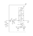
- FIG. 1 is a diagram showing a block configuration example of the transconductance amplifier 100 according to the embodiment of the present technology.
- the transconductance amplifier 100 includes a main amplifier 110, an auxiliary amplifier 120, a feedback capacitance 137, a gate capacitance 135, a load capacitance 136, a resistor 138, and an common mode feedback circuit 140. It is assumed that these are provided in the chip. An impedance matching circuit 180 is provided outside the chip.
- the main amplifier (Gm) 110 is an amplifier that converts the voltage of the input signal into a current and outputs it as an output current Iout.
- the auxiliary amplifier (Gmp) 120 is an amplifier that is branched into two from the input of the main amplifier 110 and connected in parallel.
- the gate width of the transistor of the auxiliary amplifier 120 is assumed to be, for example, about one tenth of that of the main amplifier 110. Therefore, the power consumption is about one tenth.
- the feedback capacitance (Cf) 137 is a capacitance that inverts the phase of the output of the auxiliary amplifier 120 and returns (negative feedback) to the input side.
- the gate capacitance (Cg) 135 is a capacitance that grounds the input of the auxiliary amplifier 120.
- the load capacity (Cl) 136 is a capacity for grounding the output of the auxiliary amplifier 120.
- the resistor (Rhigh) 138 is a resistor that connects the outputs of the main amplifier 110 and the auxiliary amplifier 120. The resistance value of this resistor 138 is large enough to be negligible in calculation.
- the common mode feedback circuit 140 is a common mode feedback (CMFB) circuit provided for determining the DC operating point of the outputs of the main amplifier 110 and the auxiliary amplifier 120.
- the capacitance (C6) 142 is a phase compensation capacitance for ensuring the stability of the common mode feedback loop.
- the input impedance of the common mode feedback circuit is assumed to be sufficiently high so that it can be ignored in calculation.
- the impedance matching circuit 180 is a circuit that matches the antenna impedance Rs (the signal source impedance of the input signal) with the input impedance of the auxiliary amplifier 120.
- the impedance matching circuit 180 includes a series inductor (Lm) 181 and a shunt capacitance (Cm) 182.
- a capacitor (Cdc) 193 for cutting a direct current (DC) component is provided on the input side of the impedance matching circuit 180.
- Voltage Vs is input to the transconductance amplifier 100 as an input signal. Further, here, assuming that the transconductance amplifier 100 is used in the receiving device, it is assumed that the antenna impedance Rs is, for example, 50 ⁇ .
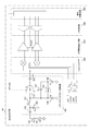
- FIG. 2 is a diagram showing a circuit configuration example of the transconductance amplifier 100 according to the embodiment of the present technology.
- the circuit configuration example shown here is basically the same as the block configuration described above. However, the bias generation circuit 150 and the electrostatic protection element 170 are not shown in the above-mentioned block configuration.
- the electrostatic protection element 170 is a circuit for protecting from a transient high voltage or high current due to electrostatic discharge (ESD: Electro-Static Discharge).
- the bias generation circuit 150 is a circuit that generates the bias voltage of the transistors of the main amplifier 110 and the auxiliary amplifier 120.
- the output of the auxiliary amplifier 120 is separated from the output of the main amplifier 110 in an alternating current (AC) by a high resistance (Rhigh) 138.
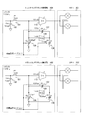
- FIG. 3 is a diagram showing a circuit configuration example of the main amplifier 110 according to the embodiment of the present technology.
- the main amplifier 110 has a configuration in which four transistors 111 to 114 are stacked in four stages.
- Transistors 111 and 114 are input transistors that receive input signals at the gate.
- HV high withstand voltage
- the bias voltages Vb1, Vb2 and Vb3 of the transistors 111, 112 and 113 are supplied from the bias generation circuit 150.
- the common mode feedback circuit 140 includes an operational amplifier 141, and feeds back the output of the main amplifier 110 to the input side of the main amplifier 110 via the resistor Rg1. Thereby, the DC potential of the output terminal is determined.
- FIG. 4 is a diagram showing a circuit configuration example of the auxiliary amplifier 120 according to the embodiment of the present technology.
- the auxiliary amplifier 120 has a configuration in which four transistors 121 to 124 are stacked in four stages.
- Transistors 121 and 124 are input transistors that receive input signals at the gate.
- Transistors 122 and 123 are output transistors that output current.
- the gate width of the transistors 121 to 124 is approximately one tenth of that of the transistors 111 to 114 of the main amplifier 110. This sets the bias current to one tenth of the main amplifier 110.
- the bias voltages Vb1, Vb2 and Vb3 of the transistors 121, 122 and 123 are common to the main amplifier 110 and are supplied from the bias generation circuit 150. Further, the common mode feedback circuit 140 that determines the DC potential of the output terminal is also shared with the main amplifier 110.
- the auxiliary amplifier 120 is loaded with a feedback capacity 137, a gate capacity 135, and a load capacity 136.
- the values of these capacitances may be variable.
- FIG. 5 is a diagram showing an example of a bias voltage generated by the bias generation circuit 150 in the embodiment of the present technology.
- This bias generation circuit 150 generates the optimum bias voltages Vb1, Vb2, Vb3 and Vref for an amplifier in which thick film transistors and thin film transistors coexist.
- the bias voltage Vb1 is supplied to the gates of the transistors 111 and 121.
- the bias voltage Vb2 is supplied to the gates of transistors 112 and 122.
- the bias voltage Vb3 is supplied to the gates of transistors 113 and 123.
- the bias voltage Vref is half the power supply voltage Vdd (Vdd / 2) and is supplied to the negative input terminal of the operational amplifier 141.
- the main amplifier 110 and the auxiliary amplifier 120 are mixed with thick-film transistors and thin film transistors stacked in four stages, but are suitable for obtaining stable characteristics even when the process, power supply voltage, and temperature fluctuate. It is necessary to apply the bias voltage. Since the variation between the thick film transistor and the thin film transistor is generally uncorrelated, it is desirable to be able to generate a bias voltage that appropriately follows the variation even when it varies independently.
- This bias generation circuit 150 is an example of realizing it.
- the transconductance amplifier 100 operates all MOSFETs in the subthreshold region.
- K is the aspect ratio (W / L) of the transistor.
- W is the gate width.
- L is the gate length.
- Vgs is the gate-source voltage.
- Vth is the threshold voltage.
- n is a subthreshold coefficient, and a typical value is about 1.7 to 1.8.
- ⁇ is the mobility.
- Cox is the gate oxide capacity.
- Vt is a thermal voltage, which is about 26 mV at room temperature of 300 K.
- the gate-source voltage Vgs is expressed by the following equation.
- Vgs n ⁇ Vt ⁇ ln (Id / (K ⁇ Is)) + Vth Therefore, the bias voltage Vb1 is given by the following equation.
- the subscript HV indicates that it is a high withstand voltage transistor.
- Vgs_MH6 n_HV ⁇ Vt ⁇ Ln ((I1 + I2) / (K_MH6 ⁇ Is_HV)) + Vth_HV
- Vgs_MH7 n_HV ⁇ Vt ⁇ ln (I2 / (K_MH7 ⁇ Is_HV)) + Vth_HV
- Vgs_MH6-Vgs_MH7 n_HV ⁇ Vt ⁇ Ln ((K_MH7 / K_MH6) (1+ (I1 / I2)))
- Vgs_ML6 n_LV ⁇ Vt ⁇ Ln (I1 / (K_ML6 ⁇ Is_LV)) + Vth_LV
- the subscript LV indicates that it is a thin film transistor.
- Vgs_MH9 n_HV ⁇ Vt ⁇ ln (I4 / (K_MH9 ⁇ Is_HV)) + Vth_HV
- Vgs_MH8 n_HV ⁇ Vt ⁇ Ln ((I4 + I5) / (K_MH8 ⁇ Is_HV)) + Vth_HV
- Vgs_ML8 n_HV ⁇ Vt ⁇ ln (I5 / (K_ML8 ⁇ Is_LV)) + Vth_LV
- the bias voltage Vref will be examined.
- the potential Vn at the connection point between the source of the transistor 156 (ML7) and the drain of the transistor 154 (ML6), and the connection point between the drain of the transistor 158 (ML8) and the source of the transistor 168 (ML9) can be expressed by the following equations.
- Vn (Vgs_MH6-Vgs_MH7) + (Vgs_ML6-Vgs_ML7)
- Vp Vdd- (Vgs_MH8-Vgs_MH9) -(Vgs_ML8-Vgs_ML9)
- Vref Vdd / 2
- bias voltages Vb1, Vb2, Vb3 and Vref By applying the bias voltages Vb1, Vb2, Vb3 and Vref in this way, stable characteristics can be obtained even when the process, power supply voltage and temperature fluctuate.
- Lm (Bp + (GpRs (Gp 2 + Bp 2 ) -Gp 2 ) 1/2 ) / ( ⁇ o (Gp 2 + Bp 2 ))
- Cm (GpRs (Gp 2 + Bp 2 ) -Gp 2 ) 1/2 / ⁇ oGpRs
- the mutual conductance Gmp of the auxiliary amplifier 120 is set to 1 mS, and the power consumption can be reduced. That is, since the auxiliary amplifier 120 does not directly generate 50 ⁇ , the power consumption is small.
- noise current of the auxiliary amplifier 120 of this embodiment goes out to the ground through the load capacitance 136. Also, peaking is applied by the impedance matching circuit 180. Therefore, the deterioration of the noise figure is small as compared with the conventional technique. Therefore, according to this embodiment, it can be seen that noise can be significantly reduced as compared with the prior art.
- the impedance matching circuit 180 since peaking is applied by the impedance matching circuit 180, it can be seen that even if an amplifier having the same transconductance (Gm) is used, the gain can be significantly improved as compared with the conventional technique.
- FIG. 6 is a diagram showing an example of a DC operating point of the transconductance amplifier 100 according to the embodiment of the present technology.
- This example shows an example in which the power supply voltage Vdd is set to 0.65V and an appropriate DC voltage is set for each part. As described above, it is assumed that each transistor stacked in four stages operates in the sub-threshold region.
- the transconductance amplifier 100 of the embodiment of the present technology includes an auxiliary amplifier 120 and an impedance matching circuit 180 which have been subjected to negative feedback by the feedback capacitance 137.
- the gain of the transconductance amplifier 100 can be improved, and power consumption and noise can be reduced.
- FIG. 7 is a diagram showing a block configuration example of the transconductance amplifier 100 in the first modification of the embodiment of the present technology.
- the transconductance amplifier 100 in this first modification divides the transconductance of the main amplifier 110 into 1: 2: 7, and is provided with a gain variable function of 0 dB, -10 dB, and -20 dB. That is, the amplifier 11 has a mutual conductance of Gm, the amplifier 12 has a mutual conductance of 2 Gm, and the amplifier 13 has a mutual conductance of 7 Gm.
- the output currents of the amplifiers 11 to 13 are added and output as the output current Iout.
- the presence or absence of operation of the amplifiers 12 and 13 is controlled by the control signals G0 and G1, respectively.
- FIG. 8 is a diagram showing an example of the relationship between the control signal and the gain of the transconductance amplifier 100 in the first modification of the embodiment of the present technology.
- G1 is “0” and G0 is “1”
- the amplifier 13 does not operate and the gain is 3 Gm ⁇ Q.
- the amplifier 12 does not operate and the gain is 8 Gm ⁇ Q.
- both G0 and G1 are "1”
- all the amplifiers 11 to 13 operate to reach 10 Gm ⁇ Q.
- the output level is based on the case where the gain is 10 Gm ⁇ Q (0 dB).
- the gain of the main amplifier 110 can be variably controlled. Even in this case, since the input impedance matching is performed by the auxiliary amplifier 120, changing the gain of the main amplifier 110 does not affect the impedance matching.
- FIG. 9 is a diagram showing a block configuration example of the transconductance amplifier 100 in the second modification of the embodiment of the present technology.
- the transconductance amplifier 100 in this second modification is obtained by dividing the mutual conductance of the main amplifier 110 by binary weighting, and has a finer gain resolution than the first modification described above.
- the gain Gain is given by the following equation.
- Gain (G0 + 2G1 + 2 2 G2 + ... + 2 N GN) ⁇ Gm ⁇ Q
- G0 to GN are gain control signals based on binary numbers of (N + 1) bits, and control the presence or absence of the corresponding amplifier operation as in the first modification described above.
- [G0 ... GN] [000 ... 0] to [111 ... 1]
- the gain of the main amplifier 110 can be variably controlled with a finer resolution.
- FIG. 10 is a diagram showing an example of a block configuration of a receiver in a third modification of the embodiment of the present technology.
- the receiver in this third modification shows an example of a GNSS receiver including the transconductance amplifier 100 of the above-described embodiment.
- a current input mixer 200, an intermediate frequency processing unit 300, an AD conversion unit 400, and a signal processing device 500 are connected to the subsequent stage of the transconductance amplifier 100.
- the signal (1720 MHz) from the LTE transmitter is close to the GPS transmission frequency (1575 MHz). Further, the transmission level from the LTE transmitter is about +25 dBm, which is higher than the GPS reception level of ⁇ 130 dBm. Therefore, the signal from the LTE transmitter can be a source of interference. In this respect, it is rather desirable that the band of the signal to be received in the GNSS receiver is narrow. Under such circumstances, it is suitable to use the transconductance amplifier 100, which can secure a wide dynamic range in the current mode operation, for the GNSS receiver.
- the current input mixer 200 multiplies the output current Iout of the transconductance amplifier 100 with the 4-phase oscillation frequency LO (Local Oscillator) to generate a low-frequency intermediate frequency (IF) signal.
- the intermediate frequency processing unit 300 includes an amplifier that amplifies the intermediate frequency signal to a predetermined level, and a filter that removes interfering waves.
- the AD conversion unit 400 converts the intermediate frequency signal processed by the intermediate frequency processing unit 300 into a digital signal.
- the signal processing device 500 uses the control signal RFAGC (Radio Frequency Automatic Gain Control) or IFAGC (Intermediate Frequency Automatic Gain Control) according to the reception level of the digital intermediate frequency signal to obtain the gain Gm of the main amplifier 110 and the intermediate frequency processing unit 300. Controls the gain of the amplifier. That is, when the reception level is higher than a predetermined threshold value, the gain of the main amplifier 110 is made relatively small. On the other hand, when the reception level is lower than the predetermined threshold value, the gain of the main amplifier 110 is relatively increased.
- the control signal RFAGC in this case can be handled according to the control signal of the first or second modification described above.
- the GNSS receiver can be configured by using the transconductance amplifier 100 of the above-described embodiment.
- the gain of the main amplifier 110 can be variably controlled by using the control signal of the first or second modification described above.
- FIG. 11 is a diagram showing a block configuration example of the transconductance amplifiers 101 and 102 in the fourth modification of the embodiment of the present technology.
- This receiver is a device that receives signals in the L1 (1.6 GHz) frequency band and the L5 (1.2 GHz) frequency band.
- the outputs of the transconductance amplifiers 101 and 102 are supplied to the current input mixers 201 and 202, respectively.
- the processing procedure described in the above-described embodiment may be regarded as a method having these series of procedures, or as a program for causing a computer to execute these series of procedures or as a recording medium for storing the program. You may catch it.
- this recording medium for example, a CD (Compact Disc), MD (MiniDisc), DVD (Digital Versatile Disc), memory card, Blu-ray Disc (Blu-ray (registered trademark) Disc) and the like can be used.
- the present technology can have the following configurations.
- a main amplifier that converts the voltage of the input signal into a current and outputs it.
- An auxiliary amplifier connected in parallel with the main amplifier, The feedback capacitance that inverts the phase of the output of the auxiliary amplifier and feeds it back to the input side, The gate capacitance for grounding the input of the auxiliary amplifier and The load capacity for grounding the output of the auxiliary amplifier and
- a transconductance amplifier including an impedance matching circuit that matches the signal source impedance of the input signal with the input impedance of the auxiliary amplifier.
- each of the main amplifier and the auxiliary amplifier includes a thick film transistor that inputs the input signal to the gate.
- each of the main amplifier and the auxiliary amplifier includes a thin film transistor having a cascode configuration in an output unit.
- the impedance matching circuit is an LC circuit including a series inductor and a shunt capacitance.
- the main amplifier that converts the voltage of the received input signal into a current and outputs it, the auxiliary amplifier connected in parallel with the main amplifier, and the output phase of the auxiliary amplifier are inverted and fed back to the input side.
- Transconductance including a feedback capacitance, a gate capacitance that grounds the input of the auxiliary amplifier, a load capacitance that grounds the output of the auxiliary amplifier, and an impedance matching circuit that matches the impedance of the input signal and the input of the auxiliary amplifier.
- a current input mixer that generates an intermediate frequency signal by multiplying the output current of the main amplifier and the output of the local oscillator.
- An intermediate frequency processing unit that amplifies the intermediate frequency signal to a predetermined level and removes interfering waves.
- An analog-to-digital converter that converts the amplified intermediate frequency signal from an analog value to a digital value
- a receiving device including a signal processing unit that performs predetermined signal processing on an intermediate frequency signal converted into a digital value. (12) The receiving device according to (11) above, which receives a signal of a global satellite positioning system as the input signal. (13) The receiving device according to (11) or (12), further comprising the plurality of transconductance amplifiers that receive signals in different frequency bands as the input signals.
Abstract
A transconductance amplifier, wherein the power consumption and noise are reduced. The transconductance amplifier is provided with a main amplifier, an auxiliary amplifier, a feedback capacitance, a gate capacitance, a load capacitance, and an impedance matching circuit. The main amplifier converts the voltage of an input signal into a current and outputs the current. The auxiliary amplifier is connected in parallel with the main amplifier. The feedback capacitance causes the output of the auxiliary amplifier to be fed back, with the phase thereof inverted, to the input side. The gate capacitance grounds the input of the auxiliary amplifier to earth. The load capacitance grounds the output of the auxiliary amplifier to earth. The impedance matching circuit causes the signal source impedance of the input signal to be matched with the input impedance of the auxiliary amplifier.
Description
本技術は、トランスコンダクタンス増幅器に関する。詳しくは、入力電圧を電流に変換するトランスコンダクタンス増幅器、および、そのトランスコンダクタンス増幅器を備える受信装置に関する。
This technology relates to a transconductance amplifier. More specifically, the present invention relates to a transconductance amplifier that converts an input voltage into an electric current, and a receiving device including the transconductance amplifier.
従来より、無線信号の受信機などにおいて、微弱な信号を増幅するために低雑音増幅器(LNA:Low Noise Amplifier)が用いられている。一方、昨今の半導体プロセス微細化の進展により、電源電圧の低下が進んでおり、増幅器の電源電圧もそれに応じて下げることが要求されている。一般に、増幅器のダイナミックレンジは、電源電圧を下げると減少する。そのため、トランスコンダクタンス増幅器を用いて、電流モードで信号処理を行う技術が知られている(例えば、非特許文献1参照。)。
Conventionally, a low noise amplifier (LNA: Low Noise Amplifier) has been used in a wireless signal receiver or the like to amplify a weak signal. On the other hand, with the recent progress in miniaturization of semiconductor processes, the power supply voltage is decreasing, and it is required to reduce the power supply voltage of the amplifier accordingly. In general, the dynamic range of an amplifier decreases as the power supply voltage decreases. Therefore, a technique for performing signal processing in a current mode using a transconductance amplifier is known (see, for example, Non-Patent Document 1).
上述の従来技術では、電流モードによる信号処理が電源電圧の制約を受けにくいことを利用して、低電源電圧におけるダイナミックレンジの改善を図っている。しかしながら、この従来技術では、帰還増幅器によるフィードバックにより入力インピーダンスが抵抗性となり、広帯域に入力整合が取れる反面、増幅器の入力に帰還増幅器のノイズが直接入力されるため、雑音指数が劣化してしまうという問題がある。また、入力整合条件を満足するために設計した場合、帰還増幅器の消費電力が著しく増加してしまうという問題がある。
In the above-mentioned conventional technology, the dynamic range at a low power supply voltage is improved by utilizing the fact that the signal processing in the current mode is not easily restricted by the power supply voltage. However, in this conventional technique, the input impedance becomes resistant due to the feedback from the feedback amplifier, and while the input can be matched over a wide band, the noise of the feedback amplifier is directly input to the input of the amplifier, so that the noise figure deteriorates. There's a problem. Further, when the design is made to satisfy the input matching condition, there is a problem that the power consumption of the feedback amplifier is remarkably increased.
本技術はこのような状況に鑑みて生み出されたものであり、トランスコンダクタンス増幅器における消費電力および雑音を低減することを目的とする。
This technology was created in view of this situation, and aims to reduce power consumption and noise in the transconductance amplifier.
本技術は、上述の問題点を解消するためになされたものであり、その第1の側面は、入力信号の電圧を電流に変換して出力する主増幅器と、上記主増幅器と並列に接続された補助増幅器と、上記補助増幅器の出力の位相を反転して入力側に帰還させる帰還容量と、上記補助増幅器の入力を接地するゲート容量と、上記補助増幅器の出力を接地する負荷容量と、上記入力信号の信号源インピーダンスと上記補助増幅器の入力インピーダンスとを整合させるインピーダンス整合回路とを具備するトランスコンダクタンス増幅器である。これにより、インピーダンス整合回路においてインピーダンスを整合させることにより、消費電力および雑音を低減させるという作用をもたらす。
This technology has been made to solve the above-mentioned problems, and the first aspect thereof is a main amplifier that converts the voltage of an input signal into a current and outputs it, and is connected in parallel with the main amplifier. The auxiliary amplifier, the feedback capacitance that inverts the phase of the output of the auxiliary amplifier and returns it to the input side, the gate capacitance that grounds the input of the auxiliary amplifier, the load capacitance that grounds the output of the auxiliary amplifier, and the above. It is a transconductance amplifier including an impedance matching circuit that matches the signal source impedance of an input signal with the input impedance of the auxiliary amplifier. This brings about the effect of reducing power consumption and noise by matching the impedance in the impedance matching circuit.
また、この第1の側面において、上記補助増幅器の出力を上記主増幅器および上記補助増幅器の入力に帰還させる同相帰還回路をさらに具備するようにしてもよい。これにより、出力端子の直流電位を定めるという作用をもたらす。
Further, in this first aspect, a common mode feedback circuit that feeds back the output of the auxiliary amplifier to the inputs of the main amplifier and the auxiliary amplifier may be further provided. This has the effect of determining the DC potential of the output terminal.
また、この第1の側面において、上記主増幅器および上記補助増幅器の各々は、上記入力信号をゲートに入力する厚膜トランジスタを備えるようにしてもよい。これにより、静電気放電によるゲート酸化膜への影響を抑制するという作用をもたらす。
Further, in this first aspect, each of the main amplifier and the auxiliary amplifier may be provided with a thick film transistor that inputs the input signal to the gate. This has the effect of suppressing the effect of electrostatic discharge on the gate oxide film.
また、この第1の側面において、上記主増幅器および上記補助増幅器の各々は、カスコード構成の薄膜トランジスタを出力部に備えるようにしてもよい。これにより、出力部の寄生容量を削減し、高周波特性を改善するという作用をもたらす。また、出力インピーダンスが高くなることにより電流出力の精度を向上させるという作用をもたらす。
Further, in this first aspect, each of the main amplifier and the auxiliary amplifier may be provided with a thin film transistor having a cascode configuration in the output unit. This has the effect of reducing the parasitic capacitance of the output section and improving the high frequency characteristics. In addition, the higher output impedance has the effect of improving the accuracy of the current output.
また、この第1の側面において、上記主増幅器および上記補助増幅器のためのバイアス電圧を生成するバイアス生成回路をさらに具備するようにしてもよい。これにより、主増幅器および補助増幅器の各部におけるバイアス電圧を適正に定めるという作用をもたらす。
Further, in this first aspect, a bias generation circuit for generating a bias voltage for the main amplifier and the auxiliary amplifier may be further provided. This has the effect of properly determining the bias voltage in each part of the main amplifier and the auxiliary amplifier.
また、この第1の側面において、上記インピーダンス整合回路は、直列インダクタおよびシャント容量を備えるLC回路であってもよい。これにより、LC回路によりインピーダンスを整合させるという作用をもたらす。
Further, in this first aspect, the impedance matching circuit may be an LC circuit having a series inductor and a shunt capacitance. This has the effect of matching the impedance with the LC circuit.
また、この第1の側面において、上記主増幅器は、並列に接続された複数の増幅器を備えるようにしてもよい。この場合において、上記複数の増幅器の少なくとも1つは、所定の制御信号に従って動作の有無を制御されるようにしてもよい。これにより、複数の増幅器の出力を組み合わせて、全体としてゲインを可変にするという作用をもたらす。また、この場合において、上記複数の増幅器の各々のゲインは、所定の固定値であってもよく、特に、他の増幅器の2倍または半分であるように設定してもよい。
Further, in this first aspect, the main amplifier may include a plurality of amplifiers connected in parallel. In this case, at least one of the plurality of amplifiers may be controlled to operate or not according to a predetermined control signal. This has the effect of combining the outputs of a plurality of amplifiers to make the gain variable as a whole. Further, in this case, the gain of each of the plurality of amplifiers may be a predetermined fixed value, and in particular, the gain may be set to be twice or half that of the other amplifiers.
また、本技術の第2の側面は、受信した入力信号の電圧を電流に変換して出力する主増幅器と、上記主増幅器と並列に接続された補助増幅器と、上記補助増幅器の出力の位相を反転して入力側に帰還させる帰還容量と、上記補助増幅器の入力を接地するゲート容量と、上記補助増幅器の出力を接地する負荷容量と、上記入力信号と上記補助増幅器の入力のインピーダンスを整合させるインピーダンス整合回路とを備えるトランスコンダクタンス増幅器と、上記主増幅器の出力電流と局部発振器の出力を乗算して中間周波数信号を生成する電流入力ミキサと、上記中間周波数信号を所定のレベルまで増幅するとともに妨害波を除去する中間周波数処理部と、上記増幅された中間周波数信号をアナログ値からデジタル値に変換するアナログデジタル変換部と、上記デジタル値に変換された中間周波数信号に所定の信号処理を施す信号処理部とを具備する受信装置である。これにより、インピーダンス整合回路においてインピーダンスを整合させたトランスコンダクタンス増幅器を用いることにより、受信装置の消費電力および雑音を低減させるという作用をもたらす。
The second aspect of the present technology is to convert the voltage of the received input signal into a current and output it, the auxiliary amplifier connected in parallel with the main amplifier, and the output phase of the auxiliary amplifier. Match the feedback capacitance that is inverted and fed back to the input side, the gate capacitance that grounds the input of the auxiliary amplifier, the load capacitance that grounds the output of the auxiliary amplifier, and the impedance of the input signal and the input of the auxiliary amplifier. A transconductance amplifier equipped with an impedance matching circuit, a current input mixer that multiplies the output current of the main amplifier by the output of the local oscillator to generate an intermediate frequency signal, and an interfering while amplifying the intermediate frequency signal to a predetermined level. An intermediate frequency processing unit that removes waves, an analog digital conversion unit that converts the amplified intermediate frequency signal from an analog value to a digital value, and a signal that performs predetermined signal processing on the intermediate frequency signal converted to the digital value. It is a receiving device including a processing unit. As a result, by using a transconductance amplifier whose impedance is matched in the impedance matching circuit, the power consumption and noise of the receiving device are reduced.
また、この第2の側面において、上記入力信号として全地球的衛星測位システム(GNSS: Global Navigation Satellite System)の信号を受信するものとしてもよい。全地球的衛星測位システムでは、高ゲイン、低雑音、低消費電力が要求される一方で、信号の帯域は狭いため、本技術のトランスコンダクタンス増幅器の適用分野として有用である。
Further, in this second aspect, a signal of a global satellite positioning system (GNSS: Global Navigation Satellite System) may be received as the above input signal. Global satellite positioning systems require high gain, low noise, and low power consumption, but have a narrow signal band, which makes them useful as applications for the transconductance amplifier of the present technology.
また、この第2の側面において、上記入力信号として互いに異なる周波数帯の信号を受ける複数の上記トランスコンダクタンス増幅器を具備してもよい。これにより、トランスコンダクタンス増幅器の各部の値の設定に応じて、異なる周波数帯の信号を同時に受信するという作用をもたらす。
Further, in the second aspect, a plurality of the transconductance amplifiers that receive signals of different frequency bands as the input signals may be provided. This brings about the effect of simultaneously receiving signals of different frequency bands according to the setting of the value of each part of the transconductance amplifier.
以下、本技術を実施するための形態(以下、実施の形態と称する)について説明する。説明は以下の順序により行う。
1.実施の形態(トランスコンダクタンス増幅器)
2.変形例 Hereinafter, embodiments for carrying out the present technology (hereinafter referred to as embodiments) will be described. The explanation will be given in the following order.
1. 1. Embodiment (transconductance amplifier)
2. Modification example
1.実施の形態(トランスコンダクタンス増幅器)
2.変形例 Hereinafter, embodiments for carrying out the present technology (hereinafter referred to as embodiments) will be described. The explanation will be given in the following order.
1. 1. Embodiment (transconductance amplifier)
2. Modification example
<1.実施の形態>
[ブロック構成]
図1は、本技術の実施の形態におけるトランスコンダクタンス増幅器100のブロック構成例を示す図である。 <1. Embodiment>
[Block configuration]
FIG. 1 is a diagram showing a block configuration example of thetransconductance amplifier 100 according to the embodiment of the present technology.
[ブロック構成]
図1は、本技術の実施の形態におけるトランスコンダクタンス増幅器100のブロック構成例を示す図である。 <1. Embodiment>
[Block configuration]
FIG. 1 is a diagram showing a block configuration example of the
このトランスコンダクタンス増幅器100は、主増幅器110と、補助増幅器120と、帰還容量137と、ゲート容量135と、負荷容量136と、抵抗138と、同相帰還回路140とを備える。これらは、チップ内に設けられることを想定する。また、チップ外には、インピーダンス整合回路180が設けられる。
The transconductance amplifier 100 includes a main amplifier 110, an auxiliary amplifier 120, a feedback capacitance 137, a gate capacitance 135, a load capacitance 136, a resistor 138, and an common mode feedback circuit 140. It is assumed that these are provided in the chip. An impedance matching circuit 180 is provided outside the chip.
主増幅器(Gm)110は、入力信号の電圧を電流に変換して、出力電流Ioutとして出力する増幅器である。
The main amplifier (Gm) 110 is an amplifier that converts the voltage of the input signal into a current and outputs it as an output current Iout.
補助増幅器(Gmp)120は、主増幅器110の入力から2分岐して並列に接続された増幅器である。この補助増幅器120のトランジスタのゲート幅は、例えば、主増幅器110の十分の一程度を想定する。したがって、消費電力も概略十分の一程度になる。
The auxiliary amplifier (Gmp) 120 is an amplifier that is branched into two from the input of the main amplifier 110 and connected in parallel. The gate width of the transistor of the auxiliary amplifier 120 is assumed to be, for example, about one tenth of that of the main amplifier 110. Therefore, the power consumption is about one tenth.
帰還容量(Cf)137は、補助増幅器120の出力の位相を反転して入力側に帰還(負帰還)させる容量である。ゲート容量(Cg)135は、補助増幅器120の入力を接地する容量である。負荷容量(Cl)136は、補助増幅器120の出力を接地する容量である。抵抗(Rhigh)138は、主増幅器110および補助増幅器120の出力を接続する抵抗である。この抵抗138の抵抗値は、計算上は無視できるほど十分大きい。
The feedback capacitance (Cf) 137 is a capacitance that inverts the phase of the output of the auxiliary amplifier 120 and returns (negative feedback) to the input side. The gate capacitance (Cg) 135 is a capacitance that grounds the input of the auxiliary amplifier 120. The load capacity (Cl) 136 is a capacity for grounding the output of the auxiliary amplifier 120. The resistor (Rhigh) 138 is a resistor that connects the outputs of the main amplifier 110 and the auxiliary amplifier 120. The resistance value of this resistor 138 is large enough to be negligible in calculation.
同相帰還回路140は、主増幅器110および補助増幅器120の出力の直流動作点を決めるために設けられたコモンモードフィードバック(Common Mode Feedback:CMFB)回路である。容量(C6)142は、同相帰還ループの安定性を確保するための位相補償容量である。なお、コモンモードフィードバック回路の入力インピーダンスは、計算上は無視できるほど十分高いものとする。
The common mode feedback circuit 140 is a common mode feedback (CMFB) circuit provided for determining the DC operating point of the outputs of the main amplifier 110 and the auxiliary amplifier 120. The capacitance (C6) 142 is a phase compensation capacitance for ensuring the stability of the common mode feedback loop. The input impedance of the common mode feedback circuit is assumed to be sufficiently high so that it can be ignored in calculation.
インピーダンス整合回路180は、アンテナインピーダンスRs(入力信号の信号源インピーダンス)と補助増幅器120の入力インピーダンスとを整合させる回路である。このインピーダンス整合回路180は、直列インダクタ(Lm)181およびシャント容量(Cm)182を備える。インピーダンス整合回路180の入力側には、直流(DC:Direct Current)成分をカットするためのコンデンサ(Cdc)193が設けられる。
The impedance matching circuit 180 is a circuit that matches the antenna impedance Rs (the signal source impedance of the input signal) with the input impedance of the auxiliary amplifier 120. The impedance matching circuit 180 includes a series inductor (Lm) 181 and a shunt capacitance (Cm) 182. A capacitor (Cdc) 193 for cutting a direct current (DC) component is provided on the input side of the impedance matching circuit 180.
トランスコンダクタンス増幅器100には、電圧Vsが入力信号として入力される。また、ここでは、トランスコンダクタンス増幅器100が受信装置に用いられることを想定して、アンテナインピーダンスRsとして例えば50Ωを想定する。
Voltage Vs is input to the transconductance amplifier 100 as an input signal. Further, here, assuming that the transconductance amplifier 100 is used in the receiving device, it is assumed that the antenna impedance Rs is, for example, 50Ω.
[回路構成]
図2は、本技術の実施の形態におけるトランスコンダクタンス増幅器100の回路構成例を示す図である。 [Circuit configuration]
FIG. 2 is a diagram showing a circuit configuration example of thetransconductance amplifier 100 according to the embodiment of the present technology.
図2は、本技術の実施の形態におけるトランスコンダクタンス増幅器100の回路構成例を示す図である。 [Circuit configuration]
FIG. 2 is a diagram showing a circuit configuration example of the
ここに示した回路構成例は、上述のブロック構成と基本的に同じものである。ただし、バイアス生成回路150および静電気保護素子170については、上述のブロック構成には示されていない。静電気保護素子170は、静電気放電(ESD:Electro-Static Discharge)による過渡的な高電圧または高電流から保護するための回路である。バイアス生成回路150は、主増幅器110および補助増幅器120のトランジスタのバイアス電圧を生成する回路である。
The circuit configuration example shown here is basically the same as the block configuration described above. However, the bias generation circuit 150 and the electrostatic protection element 170 are not shown in the above-mentioned block configuration. The electrostatic protection element 170 is a circuit for protecting from a transient high voltage or high current due to electrostatic discharge (ESD: Electro-Static Discharge). The bias generation circuit 150 is a circuit that generates the bias voltage of the transistors of the main amplifier 110 and the auxiliary amplifier 120.
また、補助増幅器120の出力は、高抵抗(Rhigh)138によって主増幅器110の出力とは交流(AC:Alternating Current)的に分離される。
Further, the output of the auxiliary amplifier 120 is separated from the output of the main amplifier 110 in an alternating current (AC) by a high resistance (Rhigh) 138.
図3は、本技術の実施の形態における主増幅器110の回路構成例を示す図である。
FIG. 3 is a diagram showing a circuit configuration example of the main amplifier 110 according to the embodiment of the present technology.
主増幅器110は、4つのトランジスタ111乃至114を4段スタックした構成を備える。トランジスタ111および114は、ゲートにおいて入力信号を受ける入力トランジスタである。これらトランジスタ111および114は、静電気放電対策のため、ゲート長の長い(例えばL=150nm)厚膜(HV:高耐圧)トランジスタ構造とする。
The main amplifier 110 has a configuration in which four transistors 111 to 114 are stacked in four stages. Transistors 111 and 114 are input transistors that receive input signals at the gate. These transistors 111 and 114 have a thick film (HV: high withstand voltage) transistor structure having a long gate length (for example, L = 150 nm) as a countermeasure against electrostatic discharge.
トランジスタ112および113は、電流を出力する出力トランジスタである。これらトランジスタ112および113は、出力部の寄生容量を削減し、さらに出力インピーダンスを高くして、電流出力の精度を向上させるため、ゲート長の短い(例えばL=40nm)薄膜(LV:低耐圧)トランジスタによるカスコード構成とする。
Transistors 112 and 113 are output transistors that output current. These transistors 112 and 113 have a short gate length (for example, L = 40 nm) thin film (LV: low withstand voltage) in order to reduce the parasitic capacitance of the output section, further increase the output impedance, and improve the accuracy of current output. It has a cascode configuration with transistors.
トランジスタ111、112および113のバイアス電圧Vb1、Vb2およびVb3は、バイアス生成回路150から供給される。
The bias voltages Vb1, Vb2 and Vb3 of the transistors 111, 112 and 113 are supplied from the bias generation circuit 150.
同相帰還回路140は、オペアンプ141を備え、主増幅器110の出力を、抵抗Rg1を介して主増幅器110の入力側にフィードバックする。これにより、出力端子の直流電位を定める。
The common mode feedback circuit 140 includes an operational amplifier 141, and feeds back the output of the main amplifier 110 to the input side of the main amplifier 110 via the resistor Rg1. Thereby, the DC potential of the output terminal is determined.
図4は、本技術の実施の形態における補助増幅器120の回路構成例を示す図である。
FIG. 4 is a diagram showing a circuit configuration example of the auxiliary amplifier 120 according to the embodiment of the present technology.
補助増幅器120は、4つのトランジスタ121乃至124を4段スタックした構成を備える。トランジスタ121および124は、ゲートにおいて入力信号を受ける入力トランジスタである。トランジスタ122および123は、電流を出力する出力トランジスタである。トランジスタ121乃至124のゲート幅は、一例として、主増幅器110のトランジスタ111乃至114の概略十分の一程度とする。これにより、バイアス電流を主増幅器110の十分の一に設定する。
The auxiliary amplifier 120 has a configuration in which four transistors 121 to 124 are stacked in four stages. Transistors 121 and 124 are input transistors that receive input signals at the gate. Transistors 122 and 123 are output transistors that output current. As an example, the gate width of the transistors 121 to 124 is approximately one tenth of that of the transistors 111 to 114 of the main amplifier 110. This sets the bias current to one tenth of the main amplifier 110.
トランジスタ121、122および123のバイアス電圧Vb1、Vb2およびVb3は、主増幅器110と共通であり、バイアス生成回路150から供給される。また、出力端子の直流電位を定める同相帰還回路140も主増幅器110と共用される。
The bias voltages Vb1, Vb2 and Vb3 of the transistors 121, 122 and 123 are common to the main amplifier 110 and are supplied from the bias generation circuit 150. Further, the common mode feedback circuit 140 that determines the DC potential of the output terminal is also shared with the main amplifier 110.
一方、主増幅器110と異なり、補助増幅器120は、帰還容量137、ゲート容量135および負荷容量136を装荷する。これらの容量の値は可変であってもよい。
On the other hand, unlike the main amplifier 110, the auxiliary amplifier 120 is loaded with a feedback capacity 137, a gate capacity 135, and a load capacity 136. The values of these capacitances may be variable.
図5は、本技術の実施の形態におけるバイアス生成回路150によって生成されるバイアス電圧の例を示す図である。
FIG. 5 is a diagram showing an example of a bias voltage generated by the bias generation circuit 150 in the embodiment of the present technology.
このバイアス生成回路150は、厚膜トランジスタと薄膜トランジスタが混在する増幅器に対し、最適なバイアス電圧Vb1、Vb2、Vb3およびVrefを生成するものである。
This bias generation circuit 150 generates the optimum bias voltages Vb1, Vb2, Vb3 and Vref for an amplifier in which thick film transistors and thin film transistors coexist.
バイアス電圧Vb1は、トランジスタ111および121のゲートに供給される。バイアス電圧Vb2は、トランジスタ112および122のゲートに供給される。バイアス電圧Vb3は、トランジスタ113および123のゲートに供給される。バイアス電圧Vrefは、後述するように、電源電圧Vddの半分(Vdd/2)であり、オペアンプ141の負入力端子に供給される。
The bias voltage Vb1 is supplied to the gates of the transistors 111 and 121. The bias voltage Vb2 is supplied to the gates of transistors 112 and 122. The bias voltage Vb3 is supplied to the gates of transistors 113 and 123. As will be described later, the bias voltage Vref is half the power supply voltage Vdd (Vdd / 2) and is supplied to the negative input terminal of the operational amplifier 141.
上述のように、主増幅器110および補助増幅器120は、厚膜トランジスタと薄膜トランジスタが4段スタックされて混在するが、プロセス、電源電圧、温度が変動した際も安定した特性を得るためには適切なバイアス電圧を印可する必要がある。厚膜トランジスタと薄膜トランジスタのばらつきは一般に相関がないため、独立にばらついた際も適切に追従するバイアス電圧が生成できることが望ましい。このバイアス生成回路150は、それを実現する一例である。
As described above, the main amplifier 110 and the auxiliary amplifier 120 are mixed with thick-film transistors and thin film transistors stacked in four stages, but are suitable for obtaining stable characteristics even when the process, power supply voltage, and temperature fluctuate. It is necessary to apply the bias voltage. Since the variation between the thick film transistor and the thin film transistor is generally uncorrelated, it is desirable to be able to generate a bias voltage that appropriately follows the variation even when it varies independently. This bias generation circuit 150 is an example of realizing it.
低消費電力化のため、トランスコンダクタンス増幅器100は全てのMOSFETをサブスレッショルド領域で動作させるものとする。MOSFETのサブスレッショルド領域における電流式は、以下の通り指数関数で表される。
Id=K・Is・exp((Vgs-Vth)/(n・Vt))
ただし、Kはトランジスタのアスペクト比(W/L)である。Wはゲート幅である。Lはゲート長である。Vgsはゲート・ソース間電圧である。Vthは閾値電圧である。 In order to reduce power consumption, thetransconductance amplifier 100 operates all MOSFETs in the subthreshold region. The current equation in the subthreshold region of the MOSFET is expressed by an exponential function as follows.
Id = K ・ Is ・ exp ((Vgs-Vth) / (n ・ Vt))
However, K is the aspect ratio (W / L) of the transistor. W is the gate width. L is the gate length. Vgs is the gate-source voltage. Vth is the threshold voltage.
Id=K・Is・exp((Vgs-Vth)/(n・Vt))
ただし、Kはトランジスタのアスペクト比(W/L)である。Wはゲート幅である。Lはゲート長である。Vgsはゲート・ソース間電圧である。Vthは閾値電圧である。 In order to reduce power consumption, the
Id = K ・ Is ・ exp ((Vgs-Vth) / (n ・ Vt))
However, K is the aspect ratio (W / L) of the transistor. W is the gate width. L is the gate length. Vgs is the gate-source voltage. Vth is the threshold voltage.
また、Isは次式により与えられる。
Is=μCox(n-1)Vt2
ここで、nはサブスレッショルド係数で、典型的な値は1.7~1.8程度である。μは移動度である。Coxはゲート酸化膜容量である。Vtは熱電圧であり、室温300Kにおいて約26mVである。 Is is also given by the following equation.
Is = μCox (n-1) Vt 2
Here, n is a subthreshold coefficient, and a typical value is about 1.7 to 1.8. μ is the mobility. Cox is the gate oxide capacity. Vt is a thermal voltage, which is about 26 mV at room temperature of 300 K.
Idの式を変形すると、ゲート・ソース間電圧Vgsは次式により表される。
Vgs=n・Vt・ln(Id/(K・Is))+Vth
したがって、バイアス電圧Vb1は次式により与えられる。
Vb1=Vgs_MH5
=n_HV・Vt・ln(I3/(K_MH5・Is_HV))+Vth_HV
ここで、添え字HVは高耐圧トランジスタであることを示す。 By modifying the equation of Id, the gate-source voltage Vgs is expressed by the following equation.
Vgs = n · Vt · ln (Id / (K · Is)) + Vth
Therefore, the bias voltage Vb1 is given by the following equation.
Vb1 = Vgs_MH5
= N_HV ・ Vt ・ ln (I3 / (K_MH5 ・ Is_HV)) + Vth_HV
Here, the subscript HV indicates that it is a high withstand voltage transistor.
次に、バイアス電圧Vb2について検討する。トランジスタ153(MH6)のゲート・ソース間電圧Vgs_MH6は次式により与えられる。
Vgs_MH6=n_HV・Vt
・ln((I1+I2)/(K_MH6・Is_HV))+Vth_HV Next, the bias voltage Vb2 will be examined. The gate-source voltage Vgs_MH6 of the transistor 153 (MH6) is given by the following equation.
Vgs_MH6 = n_HV ・ Vt
・ Ln ((I1 + I2) / (K_MH6 ・ Is_HV)) + Vth_HV
Vgs_MH6=n_HV・Vt
・ln((I1+I2)/(K_MH6・Is_HV))+Vth_HV Next, the bias voltage Vb2 will be examined. The gate-source voltage Vgs_MH6 of the transistor 153 (MH6) is given by the following equation.
Vgs_MH6 = n_HV ・ Vt
・ Ln ((I1 + I2) / (K_MH6 ・ Is_HV)) + Vth_HV
同様に、トランジスタ155(MH7)のゲート・ソース間電圧Vgs_MH7は、
Vgs_MH7=n_HV・Vt・ln(I2/(K_MH7・Is_HV))
+Vth_HV Similarly, the gate-source voltage Vgs_MH7 of the transistor 155 (MH7) is
Vgs_MH7 = n_HV ・ Vt ・ ln (I2 / (K_MH7 ・ Is_HV))
+ Vth_HV
Vgs_MH7=n_HV・Vt・ln(I2/(K_MH7・Is_HV))
+Vth_HV Similarly, the gate-source voltage Vgs_MH7 of the transistor 155 (MH7) is
Vgs_MH7 = n_HV ・ Vt ・ ln (I2 / (K_MH7 ・ Is_HV))
+ Vth_HV
上2式の差分をとると、次式が得られる。
Vgs_MH6-Vgs_MH7=n_HV・Vt
・ln((K_MH7/K_MH6)(1+(I1/I2))) By taking the difference between the above two equations, the following equation is obtained.
Vgs_MH6-Vgs_MH7 = n_HV ・ Vt
・ Ln ((K_MH7 / K_MH6) (1+ (I1 / I2)))
Vgs_MH6-Vgs_MH7=n_HV・Vt
・ln((K_MH7/K_MH6)(1+(I1/I2))) By taking the difference between the above two equations, the following equation is obtained.
Vgs_MH6-Vgs_MH7 = n_HV ・ Vt
・ Ln ((K_MH7 / K_MH6) (1+ (I1 / I2)))
また、トランジスタ154(ML6)のゲート・ソース間電圧Vgs_ML6は次式により与えられる。
Vgs_ML6=n_LV・Vt
・ln(I1/(K_ML6・Is_LV))+Vth_LV
ここで、添え字LVは薄膜トランジスタであることを示す。 Further, the gate-source voltage Vgs_ML6 of the transistor 154 (ML6) is given by the following equation.
Vgs_ML6 = n_LV ・ Vt
・ Ln (I1 / (K_ML6 ・ Is_LV)) + Vth_LV
Here, the subscript LV indicates that it is a thin film transistor.
バイアス電圧Vb2は上2式の和となるため、次式により与えられる。
Vb2=Vgs_MH6-Vgs_MH7+Vgs_ML6
=n_HV・Vt・ln((K_MH7/K_MH6)(1+(I1/I2)))
+n_LV・Vt・ln(I1/(K_ML6・Is_LV))+Vth_LV Since the bias voltage Vb2 is the sum of the above two equations, it is given by the following equation.
Vb2 = Vgs_MH6-Vgs_MH7 + Vgs_ML6
= N_HV ・ Vt ・ ln ((K_MH7 / K_MH6) (1+ (I1 / I2)))
+ N_LV ・ Vt ・ ln (I1 / (K_ML6 ・ Is_LV)) + Vth_LV
次に、バイアス電圧Vb3について検討する。トランジスタ167(MH9)のゲート・ソース間電圧Vgs_MH9は次式により与えられる。
Vgs_MH9=n_HV・Vt・ln(I4/(K_MH9・Is_HV))
+Vth_HV Next, the bias voltage Vb3 will be examined. The gate-source voltage Vgs_MH9 of the transistor 167 (MH9) is given by the following equation.
Vgs_MH9 = n_HV ・ Vt ・ ln (I4 / (K_MH9 ・ Is_HV))
+ Vth_HV
Vgs_MH9=n_HV・Vt・ln(I4/(K_MH9・Is_HV))
+Vth_HV Next, the bias voltage Vb3 will be examined. The gate-source voltage Vgs_MH9 of the transistor 167 (MH9) is given by the following equation.
Vgs_MH9 = n_HV ・ Vt ・ ln (I4 / (K_MH9 ・ Is_HV))
+ Vth_HV
また、トランジスタ157(MH8)のゲート・ソース間電圧Vgs_MH8は次式により与えられる。
Vgs_MH8=n_HV・Vt
・ln((I4+I5)/(K_MH8・Is_HV))+Vth_HV Further, the gate-source voltage Vgs_MH8 of the transistor 157 (MH8) is given by the following equation.
Vgs_MH8 = n_HV ・ Vt
・ Ln ((I4 + I5) / (K_MH8 ・ Is_HV)) + Vth_HV
Vgs_MH8=n_HV・Vt
・ln((I4+I5)/(K_MH8・Is_HV))+Vth_HV Further, the gate-source voltage Vgs_MH8 of the transistor 157 (MH8) is given by the following equation.
Vgs_MH8 = n_HV ・ Vt
・ Ln ((I4 + I5) / (K_MH8 ・ Is_HV)) + Vth_HV
また、トランジスタ158(ML8)のゲート・ソース間電圧Vgs_ML8は次式により与えられる。
Vgs_ML8=n_HV・Vt・ln(I5/(K_ML8・Is_LV))
+Vth_LV Further, the gate-source voltage Vgs_ML8 of the transistor 158 (ML8) is given by the following equation.
Vgs_ML8 = n_HV ・ Vt ・ ln (I5 / (K_ML8 ・ Is_LV))
+ Vth_LV
Vgs_ML8=n_HV・Vt・ln(I5/(K_ML8・Is_LV))
+Vth_LV Further, the gate-source voltage Vgs_ML8 of the transistor 158 (ML8) is given by the following equation.
Vgs_ML8 = n_HV ・ Vt ・ ln (I5 / (K_ML8 ・ Is_LV))
+ Vth_LV
バイアス電圧Vb3は上3式から、次式により与えられる。
Vb3=Vdd-Vgs_MH8+Vgs_MH9-Vgs_ML8
=Vdd-n_HV・Vt
・ln((K_MH8/K_MH9)(I4/(I4+I5)))
-n_LV・Vt・ln(I5/(K_ML8・Is_LV))+Vth_LV The bias voltage Vb3 is given by the following equation from the above three equations.
Vb3 = Vdd-Vgs_MH8 + Vgs_MH9-Vgs_ML8
= Vdd-n_HV · Vt
・ Ln ((K_MH8 / K_MH9) (I4 / (I4 + I5)))
-N_LV / Vt / ln (I5 / (K_ML8 / Is_LV)) + Vth_LV
次に、バイアス電圧Vrefについて検討する。バイアス生成回路150において、トランジスタ156(ML7)のソースとトランジスタ154(ML6)のドレインとの接続点の電位Vn、および、トランジスタ158(ML8)のドレインとトランジスタ168(ML9)のソースとの接続点の電位Vpの値は、それぞれ次式により表すことができる。
Vn=(Vgs_MH6-Vgs_MH7)+(Vgs_ML6-Vgs_ML7)
Vp=Vdd-(Vgs_MH8-Vgs_MH9)
-(Vgs_ML8-Vgs_ML9) Next, the bias voltage Vref will be examined. In thebias generation circuit 150, the potential Vn at the connection point between the source of the transistor 156 (ML7) and the drain of the transistor 154 (ML6), and the connection point between the drain of the transistor 158 (ML8) and the source of the transistor 168 (ML9). The value of the potential Vp of can be expressed by the following equations.
Vn = (Vgs_MH6-Vgs_MH7) + (Vgs_ML6-Vgs_ML7)
Vp = Vdd- (Vgs_MH8-Vgs_MH9)
-(Vgs_ML8-Vgs_ML9)
Vn=(Vgs_MH6-Vgs_MH7)+(Vgs_ML6-Vgs_ML7)
Vp=Vdd-(Vgs_MH8-Vgs_MH9)
-(Vgs_ML8-Vgs_ML9) Next, the bias voltage Vref will be examined. In the
Vn = (Vgs_MH6-Vgs_MH7) + (Vgs_ML6-Vgs_ML7)
Vp = Vdd- (Vgs_MH8-Vgs_MH9)
-(Vgs_ML8-Vgs_ML9)
ここで、
(Vgs_MH6-Vgs_MH7)=(Vgs_MH8-Vgs_MH9)、かつ、
(Vgs_ML6-Vgs_ML7)=(Vgs_ML8-Vgs_ML9)
となる条件を考える。 here,
(Vgs_MH6-Vgs_MH7) = (Vgs_MH8-Vgs_MH9) and
(Vgs_ML6-Vgs_ML7) = (Vgs_ML8-Vgs_ML9)
Consider the conditions that will be.
(Vgs_MH6-Vgs_MH7)=(Vgs_MH8-Vgs_MH9)、かつ、
(Vgs_ML6-Vgs_ML7)=(Vgs_ML8-Vgs_ML9)
となる条件を考える。 here,
(Vgs_MH6-Vgs_MH7) = (Vgs_MH8-Vgs_MH9) and
(Vgs_ML6-Vgs_ML7) = (Vgs_ML8-Vgs_ML9)
Consider the conditions that will be.
まず、(Vgs_MH6-Vgs_MH7)=(Vgs_MH8-Vgs_MH9)が成り立つためには、以下の条件を満たすようにトランジスタサイズおよび電流を設定する必要がある。
(K_MH7/K_MH6)(K_MH8/K_MH9)=
(I2/(I1+I2))((I4+I5)/I4) First, in order for (Vgs_MH6-Vgs_MH7) = (Vgs_MH8-Vgs_MH9) to hold, it is necessary to set the transistor size and current so as to satisfy the following conditions.
(K_MH7 / K_MH6) (K_MH8 / K_MH9) =
(I2 / (I1 + I2)) ((I4 + I5) / I4)
(K_MH7/K_MH6)(K_MH8/K_MH9)=
(I2/(I1+I2))((I4+I5)/I4) First, in order for (Vgs_MH6-Vgs_MH7) = (Vgs_MH8-Vgs_MH9) to hold, it is necessary to set the transistor size and current so as to satisfy the following conditions.
(K_MH7 / K_MH6) (K_MH8 / K_MH9) =
(I2 / (I1 + I2)) ((I4 + I5) / I4)
さらに、(Vgs_ML6-Vgs_ML7)=(Vgs_ML8-Vgs_ML9)が成り立つためには、以下の条件を満たすようにトランジスタサイズを設定する必要がある。
K_ML7/K_ML6=K_ML9/K_ML8 Further, in order for (Vgs_ML6-Vgs_ML7) = (Vgs_ML8-Vgs_ML9) to hold, it is necessary to set the transistor size so as to satisfy the following conditions.
K_ML7 / K_ML6 = K_ML9 / K_ML8
K_ML7/K_ML6=K_ML9/K_ML8 Further, in order for (Vgs_ML6-Vgs_ML7) = (Vgs_ML8-Vgs_ML9) to hold, it is necessary to set the transistor size so as to satisfy the following conditions.
K_ML7 / K_ML6 = K_ML9 / K_ML8
ここで、Rcm1=Rcm2のとき、バイアス電圧Vrefは、
Vref=(Vp+Vn)/2
で表され、Vp+Vn=Vddとなるため、バイアス電圧Vrefは、次式により与えられる。
Vref=Vdd/2 Here, when Rcm1 = Rcm2, the bias voltage Vref is
Vref = (Vp + Vn) / 2
Since it is represented by and Vp + Vn = Vdd, the bias voltage Vref is given by the following equation.
Vref = Vdd / 2
Vref=(Vp+Vn)/2
で表され、Vp+Vn=Vddとなるため、バイアス電圧Vrefは、次式により与えられる。
Vref=Vdd/2 Here, when Rcm1 = Rcm2, the bias voltage Vref is
Vref = (Vp + Vn) / 2
Since it is represented by and Vp + Vn = Vdd, the bias voltage Vref is given by the following equation.
Vref = Vdd / 2
このように各バイアス電圧Vb1、Vb2、Vb3およびVrefを印可することにより、プロセス、電源電圧、温度が変動した際も安定した特性を得ることができる。
By applying the bias voltages Vb1, Vb2, Vb3 and Vref in this way, stable characteristics can be obtained even when the process, power supply voltage and temperature fluctuate.
[入力インピーダンス]
MOSトランジスタのゲート端子における入力インピーダンスは、ほぼ容量性であるため、主増幅器110の入力アドミタンスの実部は概略ゼロである。そこで、まず、補助増幅器120の入力アドミタンスYpを求める。
Yp=(Gmp/(1+(Cl/Cf)))
+jωo(1/((1/Cf)+(1/Cl)))
ただし、ωoは、受信周波数foの角周波数である。
ωo=2πfo
ここで、実部をGpとし、虚部をBpとする。すなわち、
Yp=Gp+jBp
とする。 [Input impedance]
Since the input impedance at the gate terminal of the MOS transistor is almost capacitive, the actual part of the input admittance of themain amplifier 110 is substantially zero. Therefore, first, the input admittance Yp of the auxiliary amplifier 120 is obtained.
Yp = (Gmp / (1+ (Cl / Cf)))
+ Jωo (1 / ((1 / Cf) + (1 / Cl)))
However, ωo is an angular frequency of the reception frequency fo.
ωo = 2πfo
Here, the real part is Gp and the imaginary part is Bp. That is,
Yp = Gp + jBp
And.
MOSトランジスタのゲート端子における入力インピーダンスは、ほぼ容量性であるため、主増幅器110の入力アドミタンスの実部は概略ゼロである。そこで、まず、補助増幅器120の入力アドミタンスYpを求める。
Yp=(Gmp/(1+(Cl/Cf)))
+jωo(1/((1/Cf)+(1/Cl)))
ただし、ωoは、受信周波数foの角周波数である。
ωo=2πfo
ここで、実部をGpとし、虚部をBpとする。すなわち、
Yp=Gp+jBp
とする。 [Input impedance]
Since the input impedance at the gate terminal of the MOS transistor is almost capacitive, the actual part of the input admittance of the
Yp = (Gmp / (1+ (Cl / Cf)))
+ Jωo (1 / ((1 / Cf) + (1 / Cl)))
However, ωo is an angular frequency of the reception frequency fo.
ωo = 2πfo
Here, the real part is Gp and the imaginary part is Bp. That is,
Yp = Gp + jBp
And.
このとき、インピーダンス整合回路180の直列インダクタ181の値Lmおよびシャント容量182の値Cmは、それぞれ次式により与えられる。
Lm=(Bp+(GpRs(Gp2+Bp2)-Gp2)1/2)
/(ωo(Gp2+Bp2))
Cm=(GpRs(Gp2+Bp2)-Gp2)1/2/ωoGpRs At this time, the value Lm of theseries inductor 181 of the impedance matching circuit 180 and the value Cm of the shunt capacitance 182 are given by the following equations, respectively.
Lm = (Bp + (GpRs (Gp 2 + Bp 2 ) -Gp 2 ) 1/2 )
/ (Ωo (Gp 2 + Bp 2 ))
Cm = (GpRs (Gp 2 + Bp 2 ) -Gp 2 ) 1/2 / ωoGpRs
Lm=(Bp+(GpRs(Gp2+Bp2)-Gp2)1/2)
/(ωo(Gp2+Bp2))
Cm=(GpRs(Gp2+Bp2)-Gp2)1/2/ωoGpRs At this time, the value Lm of the
Lm = (Bp + (GpRs (Gp 2 + Bp 2 ) -Gp 2 ) 1/2 )
/ (Ωo (Gp 2 + Bp 2 ))
Cm = (GpRs (Gp 2 + Bp 2 ) -Gp 2 ) 1/2 / ωoGpRs
ここで、数値例として、
fo=1.6GHz
Gmp=1mS
Cg=0.85pF
Cf=Cl=0.2pF
とすると、
Gp=0.5mS
Bp=9.5mS
Lm=12nH
Cm=5.6pF
となる。このとき、インピーダンス整合回路180の入力から見たインピーダンスZinは、
Zin=Rs=50Ω
となり、入力インピーダンスZinをアンテナインピーダンスRsと整合させることができる。この例では、補助増幅器120の相互コンダクタンスGmpを1mSと設定しており、消費電力を低減することができる。すなわち、補助増幅器120によって直接50Ωを生成しないため、消費電力は小さい。 Here, as a numerical example,
fo = 1.6GHz
Gmp = 1mS
Cg = 0.85pF
Cf = Cl = 0.2pF
Then
Gp = 0.5mS
Bp = 9.5mS
Lm = 12nH
Cm = 5.6pF
Will be. At this time, the impedance Zin seen from the input of theimpedance matching circuit 180 is
Zin = Rs = 50Ω
Therefore, the input impedance Zin can be matched with the antenna impedance Rs. In this example, the mutual conductance Gmp of theauxiliary amplifier 120 is set to 1 mS, and the power consumption can be reduced. That is, since the auxiliary amplifier 120 does not directly generate 50Ω, the power consumption is small.
fo=1.6GHz
Gmp=1mS
Cg=0.85pF
Cf=Cl=0.2pF
とすると、
Gp=0.5mS
Bp=9.5mS
Lm=12nH
Cm=5.6pF
となる。このとき、インピーダンス整合回路180の入力から見たインピーダンスZinは、
Zin=Rs=50Ω
となり、入力インピーダンスZinをアンテナインピーダンスRsと整合させることができる。この例では、補助増幅器120の相互コンダクタンスGmpを1mSと設定しており、消費電力を低減することができる。すなわち、補助増幅器120によって直接50Ωを生成しないため、消費電力は小さい。 Here, as a numerical example,
fo = 1.6GHz
Gmp = 1mS
Cg = 0.85pF
Cf = Cl = 0.2pF
Then
Gp = 0.5mS
Bp = 9.5mS
Lm = 12nH
Cm = 5.6pF
Will be. At this time, the impedance Zin seen from the input of the
Zin = Rs = 50Ω
Therefore, the input impedance Zin can be matched with the antenna impedance Rs. In this example, the mutual conductance Gmp of the
一方、従来技術のように、帰還増幅器(Gmf)によるフィードバックを行った場合には、入力インピーダンスは「1/Gmf」となる。これを50Ωに整合させるためには、Gmfを20mSにする以外に選択の余地はなく、消費電力が増大してしまう。
On the other hand, when feedback is performed by a feedback amplifier (Gmf) as in the prior art, the input impedance is "1 / Gmf". In order to match this with 50Ω, there is no choice but to set Gmf to 20mS, and the power consumption increases.
したがって、この実施の形態によれば、従来技術よりも大幅に消費電力を低減できることがわかる。
Therefore, according to this embodiment, it can be seen that the power consumption can be significantly reduced as compared with the conventional technique.
[雑音指数]
上述のように入力インピーダンスの整合をとった場合、インピーダンス整合回路180の雑音指数NF(Noise Figure)は、次式により与えられる。なお、LmのQ値は十分大きく、損失は無視できるものと仮定する。
NF=10log10(1+(γ/(1+Cl/Cf))
(1+4Gmp/Gm))
ただし、γはMOSFETの熱雑音係数で、約「2/3」である。 [Noise figure]
When the input impedance is matched as described above, the noise figure NF (Noise Figure) of theimpedance matching circuit 180 is given by the following equation. It is assumed that the Q value of Lm is sufficiently large and the loss is negligible.
NF = 10 log 10 (1+ (γ / (1 + Cl / Cf)))
(1 + 4Gmp / Gm))
However, γ is the thermal noise coefficient of the MOSFET, which is about “2/3”.
上述のように入力インピーダンスの整合をとった場合、インピーダンス整合回路180の雑音指数NF(Noise Figure)は、次式により与えられる。なお、LmのQ値は十分大きく、損失は無視できるものと仮定する。
NF=10log10(1+(γ/(1+Cl/Cf))
(1+4Gmp/Gm))
ただし、γはMOSFETの熱雑音係数で、約「2/3」である。 [Noise figure]
When the input impedance is matched as described above, the noise figure NF (Noise Figure) of the
NF = 10 log 10 (1+ (γ / (1 + Cl / Cf)))
(1 + 4Gmp / Gm))
However, γ is the thermal noise coefficient of the MOSFET, which is about “2/3”.
ここで、数値例として、
Gm=10mS
Gmp=1mS
Cf=Cl=0.2pF
を上式に代入すると、NF=1.67dBとなる。 Here, as a numerical example,
Gm = 10mS
Gmp = 1mS
Cf = Cl = 0.2pF
Is substituted into the above equation, and NF = 1.67 dB.
Gm=10mS
Gmp=1mS
Cf=Cl=0.2pF
を上式に代入すると、NF=1.67dBとなる。 Here, as a numerical example,
Gm = 10mS
Gmp = 1mS
Cf = Cl = 0.2pF
Is substituted into the above equation, and NF = 1.67 dB.
一方、従来技術のように、帰還増幅器によるフィードバックを行った場合には、雑音指数NFは、
NF=10log10(1+γ(1+4/GmRs))
となり、上述のGmf=20mSを用いると、NF=8.45dBとなる。 On the other hand, when feedback is performed by a feedback amplifier as in the prior art, the noise figure NF is
NF = 10 log 10 (1 + γ (1 + 4 / GmRs))
Therefore, when the above-mentioned Gmf = 20 mS is used, NF = 8.45 dB.
NF=10log10(1+γ(1+4/GmRs))
となり、上述のGmf=20mSを用いると、NF=8.45dBとなる。 On the other hand, when feedback is performed by a feedback amplifier as in the prior art, the noise figure NF is
NF = 10 log 10 (1 + γ (1 + 4 / GmRs))
Therefore, when the above-mentioned Gmf = 20 mS is used, NF = 8.45 dB.
すなわち、この実施の形態の補助増幅器120のノイズ電流は、その一部が負荷容量136を通してグラウンドに抜ける。また、インピーダンス整合回路180によってピーキングがかかる。そのため、従来技術と比べて雑音指数の劣化が小さい。したがって、この実施の形態によれば、従来技術よりも大幅にノイズを低減できることがわかる。
That is, a part of the noise current of the auxiliary amplifier 120 of this embodiment goes out to the ground through the load capacitance 136. Also, peaking is applied by the impedance matching circuit 180. Therefore, the deterioration of the noise figure is small as compared with the conventional technique. Therefore, according to this embodiment, it can be seen that noise can be significantly reduced as compared with the prior art.
[トランスコンダクタンスゲイン]
上述のように入力インピーダンスの整合をとった場合、トランスコンダクタンスゲインGainは、次式により与えられる。
Gain=Iout/Vs
=(Gm/2)((1+Cl/Cf)/RsGmp)1/2 [Transconductance gain]
When the input impedance is matched as described above, the transconductance gain Gain is given by the following equation.
Gain = Iout / Vs
= (Gm / 2) ((1 + Cl / Cf) / RsGmp) 1/2
ここで、数値例として、
Rs=50Ω
Gm=10mS
Gmp=1mS
Cf=Cl=0.2pF
を上式に代入すると、Gain=31.5mA/Vとなる。 Here, as a numerical example,
Rs = 50Ω
Gm = 10mS
Gmp = 1mS
Cf = Cl = 0.2pF
Is substituted into the above equation, Gain = 31.5 mA / V.
Rs=50Ω
Gm=10mS
Gmp=1mS
Cf=Cl=0.2pF
を上式に代入すると、Gain=31.5mA/Vとなる。 Here, as a numerical example,
Rs = 50Ω
Gm = 10mS
Gmp = 1mS
Cf = Cl = 0.2pF
Is substituted into the above equation, Gain = 31.5 mA / V.
一方、従来技術のように、帰還増幅器によるフィードバックを行った場合には、トランスコンダクタンスゲインGainは、
Gain=Iout/Vs
=Gm/(1+RsGmf)
=Gm/2
となり、上述のGm=10mSを用いると、Gain=5mA/Vとなる。 On the other hand, when feedback is performed by a feedback amplifier as in the prior art, the transconductance gain Gain is
Gain = Iout / Vs
= Gm / (1 + RsGmf)
= Gm / 2
Therefore, when the above-mentioned Gm = 10 mS is used, Gain = 5 mA / V.
したがって、この実施の形態によれば、インピーダンス整合回路180によってピーキングがかかるため、相互コンダクタンス(Gm)が同じ増幅器を用いたとしても、従来技術よりも大幅にゲインを向上させることができることがわかる。
Therefore, according to this embodiment, since peaking is applied by the impedance matching circuit 180, it can be seen that even if an amplifier having the same transconductance (Gm) is used, the gain can be significantly improved as compared with the conventional technique.
[直流動作点]
図6は、本技術の実施の形態におけるトランスコンダクタンス増幅器100の直流動作点の一例を示す図である。 [DC operating point]
FIG. 6 is a diagram showing an example of a DC operating point of thetransconductance amplifier 100 according to the embodiment of the present technology.
図6は、本技術の実施の形態におけるトランスコンダクタンス増幅器100の直流動作点の一例を示す図である。 [DC operating point]
FIG. 6 is a diagram showing an example of a DC operating point of the
この例は、電源電圧Vddを0.65Vとして、各部に適切な直流電圧を設定する例を示している。上述のように、4段積みされた各トランジスタは、サブスレショルド領域で動作するものと想定している。
This example shows an example in which the power supply voltage Vdd is set to 0.65V and an appropriate DC voltage is set for each part. As described above, it is assumed that each transistor stacked in four stages operates in the sub-threshold region.
このように、本技術の実施の形態のトランスコンダクタンス増幅器100は、帰還容量137により負帰還を施した補助増幅器120およびインピーダンス整合回路180を備える。これにより、トランスコンダクタンス増幅器100のゲインを向上させるとともに、消費電力および雑音を低減することができる。
As described above, the transconductance amplifier 100 of the embodiment of the present technology includes an auxiliary amplifier 120 and an impedance matching circuit 180 which have been subjected to negative feedback by the feedback capacitance 137. As a result, the gain of the transconductance amplifier 100 can be improved, and power consumption and noise can be reduced.
<2.変形例>
[第1の変形例]
図7は、本技術の実施の形態の第1の変形例におけるトランスコンダクタンス増幅器100のブロック構成例を示す図である。 <2. Modification example>
[First modification]
FIG. 7 is a diagram showing a block configuration example of thetransconductance amplifier 100 in the first modification of the embodiment of the present technology.
[第1の変形例]
図7は、本技術の実施の形態の第1の変形例におけるトランスコンダクタンス増幅器100のブロック構成例を示す図である。 <2. Modification example>
[First modification]
FIG. 7 is a diagram showing a block configuration example of the
この第1の変形例におけるトランスコンダクタンス増幅器100は、主増幅器110の相互コンダクタンスを1:2:7に分割し、0dB、-10dB、-20dBのゲイン可変機能を設けたものである。すなわち、増幅器11はGm、増幅器12は2Gm、増幅器13は7Gmの相互コンダクタンスを有する。
The transconductance amplifier 100 in this first modification divides the transconductance of the main amplifier 110 into 1: 2: 7, and is provided with a gain variable function of 0 dB, -10 dB, and -20 dB. That is, the amplifier 11 has a mutual conductance of Gm, the amplifier 12 has a mutual conductance of 2 Gm, and the amplifier 13 has a mutual conductance of 7 Gm.
増幅器11乃至13の出力電流は加算されて、出力電流Ioutとして出力される。増幅器12および13は、それぞれ制御信号G0およびG1によって、動作の有無が制御される。
The output currents of the amplifiers 11 to 13 are added and output as the output current Iout. The presence or absence of operation of the amplifiers 12 and 13 is controlled by the control signals G0 and G1, respectively.
図8は、本技術の実施の形態の第1の変形例におけるトランスコンダクタンス増幅器100の制御信号とゲインの関係例を示す図である。
FIG. 8 is a diagram showing an example of the relationship between the control signal and the gain of the transconductance amplifier 100 in the first modification of the embodiment of the present technology.
制御信号G0およびG1は、それぞれ増幅器12および13の動作の有無を制御する信号である。G0およびG1がともに「0」であれば、増幅器12および13は動作せず、増幅器11のみが動作して、ゲインはGm・Qとなる。なお、Qは次式に与えられる。
Q=(1/2)((1+Cl/Cf)/RsGmp)1/2 The control signals G0 and G1 are signals for controlling the presence / absence of operation of the amplifiers 12 and 13, respectively. If both G0 and G1 are "0", the amplifiers 12 and 13 do not operate, only the amplifier 11 operates, and the gain becomes Gm · Q. Q is given by the following equation.
Q = (1/2) ((1 + Cl / Cf) / RsGmp) 1/2
Q=(1/2)((1+Cl/Cf)/RsGmp)1/2 The control signals G0 and G1 are signals for controlling the presence / absence of operation of the
Q = (1/2) ((1 + Cl / Cf) / RsGmp) 1/2
G1が「0」でG0が「1」であれば、増幅器13は動作せず、ゲインは3Gm・Qとなる。同様に、G1が「1」でG0が「0」であれば、増幅器12は動作せず、ゲインは8Gm・Qとなる。また、G0およびG1がともに「1」であれば、増幅器11乃至13が全て動作して10Gm・Qとなる。なお、出力レベルは、ゲインが10Gm・Qの場合を基準(0dB)としている。
If G1 is "0" and G0 is "1", the amplifier 13 does not operate and the gain is 3 Gm · Q. Similarly, if G1 is "1" and G0 is "0", the amplifier 12 does not operate and the gain is 8 Gm · Q. If both G0 and G1 are "1", all the amplifiers 11 to 13 operate to reach 10 Gm · Q. The output level is based on the case where the gain is 10 Gm · Q (0 dB).
このように、この実施の形態の第1の変形例によれば、主増幅器110のゲインを可変に制御することができる。この場合においても、入力インピーダンス整合は補助増幅器120で取っているため、主増幅器110のゲインを変えてもインピーダンスの整合に影響を及ぼさない。
As described above, according to the first modification of this embodiment, the gain of the main amplifier 110 can be variably controlled. Even in this case, since the input impedance matching is performed by the auxiliary amplifier 120, changing the gain of the main amplifier 110 does not affect the impedance matching.
[第2の変形例]
図9は、本技術の実施の形態の第2の変形例におけるトランスコンダクタンス増幅器100のブロック構成例を示す図である。 [Second variant]
FIG. 9 is a diagram showing a block configuration example of thetransconductance amplifier 100 in the second modification of the embodiment of the present technology.
図9は、本技術の実施の形態の第2の変形例におけるトランスコンダクタンス増幅器100のブロック構成例を示す図である。 [Second variant]
FIG. 9 is a diagram showing a block configuration example of the
この第2の変形例におけるトランスコンダクタンス増幅器100は、主増幅器110の相互コンダクタンスを2進数の重み付けにより分割したものであり、上述の第1の変形例よりも細かいゲイン分解能を備える。
The transconductance amplifier 100 in this second modification is obtained by dividing the mutual conductance of the main amplifier 110 by binary weighting, and has a finer gain resolution than the first modification described above.
この第2の変形例では、ゲインGainは、次式により与えられる。
Gain=(G0+2G1+22G2+…+2NGN)・Gm・Q
ここで、G0乃至GNは、(N+1)ビットの2進数によるゲイン制御信号であり、上述の第1の変形例と同様に、対応する増幅器の動作の有無を制御するものである。
[G0…GN]=[000…0]~[111…1] In this second modification, the gain Gain is given by the following equation.
Gain = (G0 + 2G1 + 2 2 G2 + ... + 2 N GN) ・ Gm ・ Q
Here, G0 to GN are gain control signals based on binary numbers of (N + 1) bits, and control the presence or absence of the corresponding amplifier operation as in the first modification described above.
[G0 ... GN] = [000 ... 0] to [111 ... 1]
このように、この実施の形態の第2の変形例によれば、主増幅器110のゲインをより細かい分解能により可変に制御することができる。
As described above, according to the second modification of this embodiment, the gain of the main amplifier 110 can be variably controlled with a finer resolution.
[第3の変形例]
図10は、本技術の実施の形態の第3の変形例における受信機のブロック構成例を示す図である。 [Third variant]
FIG. 10 is a diagram showing an example of a block configuration of a receiver in a third modification of the embodiment of the present technology.
図10は、本技術の実施の形態の第3の変形例における受信機のブロック構成例を示す図である。 [Third variant]
FIG. 10 is a diagram showing an example of a block configuration of a receiver in a third modification of the embodiment of the present technology.
この第3の変形例における受信機は、上述の実施の形態のトランスコンダクタンス増幅器100を備えるGNSS受信機の一例を示している。このGNSS受信機では、トランスコンダクタンス増幅器100の後段には、電流入力ミキサ200、中間周波数処理部300、AD変換部400、および、信号処理装置500が接続される。
The receiver in this third modification shows an example of a GNSS receiver including the transconductance amplifier 100 of the above-described embodiment. In this GNSS receiver, a current input mixer 200, an intermediate frequency processing unit 300, an AD conversion unit 400, and a signal processing device 500 are connected to the subsequent stage of the transconductance amplifier 100.
GNSS受信機とLTE(Long Term Evolution)送信機が同一筐体内に混載されるような場合、LTE送信機からの信号(1720MHz)はGPSの送信周波数(1575MHz)に近い。また、LTE送信機からの送信レベルは+25dBm程度であり、GPSの受信レベル-130dBmよりも大きい。したがって、LTE送信機からの信号は妨害源となり得る。この点、GNSS受信機において受信対象となる信号の帯域は狭い方がむしろ望ましい。このような状況下では、電流モード動作で、ダイナミックレンジを広く確保できるトランスコンダクタンス増幅器100をGNSS受信機に用いるのに適している。
When the GNSS receiver and the LTE (Long Term Evolution) transmitter are mounted together in the same housing, the signal (1720 MHz) from the LTE transmitter is close to the GPS transmission frequency (1575 MHz). Further, the transmission level from the LTE transmitter is about +25 dBm, which is higher than the GPS reception level of −130 dBm. Therefore, the signal from the LTE transmitter can be a source of interference. In this respect, it is rather desirable that the band of the signal to be received in the GNSS receiver is narrow. Under such circumstances, it is suitable to use the transconductance amplifier 100, which can secure a wide dynamic range in the current mode operation, for the GNSS receiver.
電流入力ミキサ200は、トランスコンダクタンス増幅器100の出力電流Ioutと4相の発振周波数LO(Local Oscillator)を乗算して、低周波数の中間周波数(IF:Intermediate Frequency)信号を生成するものである。中間周波数処理部300は、中間周波数信号を所定のレベルまで増幅する増幅器、および、妨害波を除去するフィルタを備える。AD変換部400は、中間周波数処理部300によって処理された中間周波数信号をデジタル信号に変換するものである。
The current input mixer 200 multiplies the output current Iout of the transconductance amplifier 100 with the 4-phase oscillation frequency LO (Local Oscillator) to generate a low-frequency intermediate frequency (IF) signal. The intermediate frequency processing unit 300 includes an amplifier that amplifies the intermediate frequency signal to a predetermined level, and a filter that removes interfering waves. The AD conversion unit 400 converts the intermediate frequency signal processed by the intermediate frequency processing unit 300 into a digital signal.
信号処理装置500は、デジタルの中間周波数信号の受信レベルに応じた制御信号RFAGC(Radio Frequency Automatic Gain Control)またはIFAGC(Intermediate Frequency Automatic Gain Control)により、主増幅器110のゲインGmおよび中間周波数処理部300の増幅器のゲインを制御する。すなわち、受信レベルが所定の閾値より高い場合には、主増幅器110のゲインを相対的に小さくする。一方、受信レベルが所定の閾値より以下の場合には、主増幅器110のゲインを相対的に大きくする。この場合の制御信号RFAGCは、上述の第1または第2の変形例の制御信号に準じて扱うことができる。
The signal processing device 500 uses the control signal RFAGC (Radio Frequency Automatic Gain Control) or IFAGC (Intermediate Frequency Automatic Gain Control) according to the reception level of the digital intermediate frequency signal to obtain the gain Gm of the main amplifier 110 and the intermediate frequency processing unit 300. Controls the gain of the amplifier. That is, when the reception level is higher than a predetermined threshold value, the gain of the main amplifier 110 is made relatively small. On the other hand, when the reception level is lower than the predetermined threshold value, the gain of the main amplifier 110 is relatively increased. The control signal RFAGC in this case can be handled according to the control signal of the first or second modification described above.
このように、この実施の形態の第3の変形例によれば、上述の実施の形態のトランスコンダクタンス増幅器100を利用してGNSS受信機を構成することができる。これにより、例えばGNSS受信機とLTE送信機が同一筐体内に混載されるような場合においても、大出力のLTE送信信号によるGNSS信号の歪みを抑制して、良好な測位精度を得ることができる。また、この場合において、上述の第1または第2の変形例の制御信号を利用して主増幅器110のゲインを可変制御することができる。
As described above, according to the third modification of this embodiment, the GNSS receiver can be configured by using the transconductance amplifier 100 of the above-described embodiment. Thereby, for example, even when the GNSS receiver and the LTE transmitter are mixedly mounted in the same housing, the distortion of the GNSS signal due to the high output LTE transmission signal can be suppressed and good positioning accuracy can be obtained. .. Further, in this case, the gain of the main amplifier 110 can be variably controlled by using the control signal of the first or second modification described above.
[第4の変形例]
図11は、本技術の実施の形態の第4の変形例におけるトランスコンダクタンス増幅器101および102のブロック構成例を示す図である。 [Fourth variant]
FIG. 11 is a diagram showing a block configuration example of thetransconductance amplifiers 101 and 102 in the fourth modification of the embodiment of the present technology.
図11は、本技術の実施の形態の第4の変形例におけるトランスコンダクタンス増幅器101および102のブロック構成例を示す図である。 [Fourth variant]
FIG. 11 is a diagram showing a block configuration example of the
ここでは、上述の実施の形態におけるトランスコンダクタンス増幅器100を2台備えるデュアルバンドGNSS受信機の一例を示している。この受信機は、L1(1.6GHz)周波数帯およびL5(1.2GHz)周波数帯の信号を受信する装置である。トランスコンダクタンス増幅器101および102の出力は、それぞれ電流入力ミキサ201および202に供給される。
Here, an example of a dual band GNSS receiver including two transformer conductance amplifiers 100 in the above-described embodiment is shown. This receiver is a device that receives signals in the L1 (1.6 GHz) frequency band and the L5 (1.2 GHz) frequency band. The outputs of the transconductance amplifiers 101 and 102 are supplied to the current input mixers 201 and 202, respectively.
このデュアルバンドGNSS受信機では、直列インダクタ181、シャント容量182、ゲート容量135、帰還容量137および負荷容量136に、周波数帯毎に最適化された異なる値を設定する。この例では、L1周波数帯では、Lm=12nH、Cm=5.6pF、Cg=0.85pF、Cf=Cl=0.2pFを設定している。また、L5周波数帯では、Lm=16nH、Cm=7.5pF、Cg=1.1pF、Cf=Cl=0.26pFを設定している。このような設定におけるSpiceシミュレーションを行った結果、L1周波数帯およびL5周波数帯のそれぞれにおいて、十分な利得が得られ、また、電圧定在波比VSWR=1.5程度の良好なインピーダンスマッチング特性が得られることを確認している。
In this dual band GNSS receiver, different values optimized for each frequency band are set for the series inductor 181, the shunt capacity 182, the gate capacity 135, the feedback capacity 137, and the load capacity 136. In this example, in the L1 frequency band, Lm = 12nH, Cm = 5.6pF, Cg = 0.85pF, and Cf = Cl = 0.2pF are set. Further, in the L5 frequency band, Lm = 16nH, Cm = 7.5pF, Cg = 1.1pF, and Cf = Cl = 0.26pF are set. As a result of performing a Spice simulation with such a setting, sufficient gain is obtained in each of the L1 frequency band and the L5 frequency band, and good impedance matching characteristics with a voltage standing wave ratio VSWR = 1.5 are obtained. I have confirmed that it can be obtained.
このように、この実施の形態の第4の変形例によれば、各部の値を適切に設定することにより、複数の周波数帯において、それぞれ十分な利得および良好なインピーダンスマッチング特性を得ることができる。
As described above, according to the fourth modification of this embodiment, by appropriately setting the values of each part, sufficient gain and good impedance matching characteristics can be obtained in each of a plurality of frequency bands. ..
なお、上述の実施の形態は本技術を具現化するための一例を示したものであり、実施の形態における事項と、特許請求の範囲における発明特定事項とはそれぞれ対応関係を有する。同様に、特許請求の範囲における発明特定事項と、これと同一名称を付した本技術の実施の形態における事項とはそれぞれ対応関係を有する。ただし、本技術は実施の形態に限定されるものではなく、その要旨を逸脱しない範囲において実施の形態に種々の変形を施すことにより具現化することができる。
Note that the above-described embodiment shows an example for embodying the present technology, and the matters in the embodiment and the matters specifying the invention in the claims have a corresponding relationship with each other. Similarly, the matters specifying the invention within the scope of claims and the matters in the embodiment of the present technology having the same name have a corresponding relationship with each other. However, the present technology is not limited to the embodiment, and can be embodied by applying various modifications to the embodiment without departing from the gist thereof.
また、上述の実施の形態において説明した処理手順は、これら一連の手順を有する方法として捉えてもよく、また、これら一連の手順をコンピュータに実行させるためのプログラム乃至そのプログラムを記憶する記録媒体として捉えてもよい。この記録媒体として、例えば、CD(Compact Disc)、MD(MiniDisc)、DVD(Digital Versatile Disc)、メモリカード、ブルーレイディスク(Blu-ray(登録商標)Disc)等を用いることができる。
Further, the processing procedure described in the above-described embodiment may be regarded as a method having these series of procedures, or as a program for causing a computer to execute these series of procedures or as a recording medium for storing the program. You may catch it. As this recording medium, for example, a CD (Compact Disc), MD (MiniDisc), DVD (Digital Versatile Disc), memory card, Blu-ray Disc (Blu-ray (registered trademark) Disc) and the like can be used.
なお、本明細書に記載された効果はあくまで例示であって、限定されるものではなく、また、他の効果があってもよい。
It should be noted that the effects described in the present specification are merely examples and are not limited, and other effects may be obtained.
なお、本技術は以下のような構成もとることができる。
(1)入力信号の電圧を電流に変換して出力する主増幅器と、
前記主増幅器と並列に接続された補助増幅器と、
前記補助増幅器の出力の位相を反転して入力側に帰還させる帰還容量と、
前記補助増幅器の入力を接地するゲート容量と、
前記補助増幅器の出力を接地する負荷容量と、
前記入力信号の信号源インピーダンスと前記補助増幅器の入力インピーダンスとを整合させるインピーダンス整合回路と
を具備するトランスコンダクタンス増幅器。
(2)前記補助増幅器の出力を前記主増幅器および前記補助増幅器の入力に帰還させる同相帰還回路をさらに具備する
前記(1)に記載のトランスコンダクタンス増幅器。
(3)前記主増幅器および前記補助増幅器の各々は、前記入力信号をゲートに入力する厚膜トランジスタを備える
前記(1)または(2)に記載のトランスコンダクタンス増幅器。
(4)前記主増幅器および前記補助増幅器の各々は、カスコード構成の薄膜トランジスタを出力部に備える
前記(1)から(3)のいずれかに記載のトランスコンダクタンス増幅器。
(5)前記主増幅器および前記補助増幅器のためのバイアス電圧を生成するバイアス生成回路をさらに具備する
前記(1)から(4)のいずれかに記載のトランスコンダクタンス増幅器。
(6)前記インピーダンス整合回路は、直列インダクタおよびシャント容量を備えるLC回路である
前記(1)から(5)のいずれかに記載のトランスコンダクタンス増幅器。
(7)前記主増幅器は、並列に接続された複数の増幅器を備える
前記(1)から(6)のいずれかに記載のトランスコンダクタンス増幅器。
(8)前記複数の増幅器の少なくとも1つは、所定の制御信号に従って動作の有無を制御される
前記(7)に記載のトランスコンダクタンス増幅器。
(9)前記複数の増幅器の各々のゲインは、所定の固定値である
前記(7)または(8)に記載のトランスコンダクタンス増幅器。
(10)前記複数の増幅器の各々のゲインは、他の増幅器の2倍または半分である
前記(7)または(8)に記載のトランスコンダクタンス増幅器。
(11)受信した入力信号の電圧を電流に変換して出力する主増幅器と、前記主増幅器と並列に接続された補助増幅器と、前記補助増幅器の出力の位相を反転して入力側に帰還させる帰還容量と、前記補助増幅器の入力を接地するゲート容量と、前記補助増幅器の出力を接地する負荷容量と、前記入力信号と前記補助増幅器の入力のインピーダンスを整合させるインピーダンス整合回路とを備えるトランスコンダクタンス増幅器と、
前記主増幅器の出力電流と局部発振器の出力を乗算して中間周波数信号を生成する電流入力ミキサと、
前記中間周波数信号を所定のレベルまで増幅するとともに妨害波を除去する中間周波数処理部と、
前記増幅された中間周波数信号をアナログ値からデジタル値に変換するアナログデジタル変換部と、
前記デジタル値に変換された中間周波数信号に所定の信号処理を施す信号処理部と
を具備する受信装置。
(12)前記入力信号として全地球的衛星測位システムの信号を受信する
前記(11)に記載の受信装置。
(13)前記入力信号として互いに異なる周波数帯の信号を受ける複数の前記トランスコンダクタンス増幅器を具備する前記(11)または(12)に記載の受信装置。 The present technology can have the following configurations.
(1) A main amplifier that converts the voltage of the input signal into a current and outputs it.
An auxiliary amplifier connected in parallel with the main amplifier,
The feedback capacitance that inverts the phase of the output of the auxiliary amplifier and feeds it back to the input side,
The gate capacitance for grounding the input of the auxiliary amplifier and
The load capacity for grounding the output of the auxiliary amplifier and
A transconductance amplifier including an impedance matching circuit that matches the signal source impedance of the input signal with the input impedance of the auxiliary amplifier.
(2) The transconductance amplifier according to (1), further comprising an in-phase feedback circuit that feeds back the output of the auxiliary amplifier to the inputs of the main amplifier and the auxiliary amplifier.
(3) The transconductance amplifier according to (1) or (2) above, wherein each of the main amplifier and the auxiliary amplifier includes a thick film transistor that inputs the input signal to the gate.
(4) The transconductance amplifier according to any one of (1) to (3) above, wherein each of the main amplifier and the auxiliary amplifier includes a thin film transistor having a cascode configuration in an output unit.
(5) The transconductance amplifier according to any one of (1) to (4), further comprising a bias generation circuit for generating a bias voltage for the main amplifier and the auxiliary amplifier.
(6) The transconductance amplifier according to any one of (1) to (5) above, wherein the impedance matching circuit is an LC circuit including a series inductor and a shunt capacitance.
(7) The transconductance amplifier according to any one of (1) to (6) above, wherein the main amplifier includes a plurality of amplifiers connected in parallel.
(8) The transconductance amplifier according to (7), wherein at least one of the plurality of amplifiers is controlled to operate or not according to a predetermined control signal.
(9) The transconductance amplifier according to (7) or (8), wherein the gain of each of the plurality of amplifiers is a predetermined fixed value.
(10) The transconductance amplifier according to (7) or (8), wherein the gain of each of the plurality of amplifiers is twice or half that of the other amplifiers.
(11) The main amplifier that converts the voltage of the received input signal into a current and outputs it, the auxiliary amplifier connected in parallel with the main amplifier, and the output phase of the auxiliary amplifier are inverted and fed back to the input side. Transconductance including a feedback capacitance, a gate capacitance that grounds the input of the auxiliary amplifier, a load capacitance that grounds the output of the auxiliary amplifier, and an impedance matching circuit that matches the impedance of the input signal and the input of the auxiliary amplifier. With an amplifier
A current input mixer that generates an intermediate frequency signal by multiplying the output current of the main amplifier and the output of the local oscillator.
An intermediate frequency processing unit that amplifies the intermediate frequency signal to a predetermined level and removes interfering waves.
An analog-to-digital converter that converts the amplified intermediate frequency signal from an analog value to a digital value,
A receiving device including a signal processing unit that performs predetermined signal processing on an intermediate frequency signal converted into a digital value.
(12) The receiving device according to (11) above, which receives a signal of a global satellite positioning system as the input signal.
(13) The receiving device according to (11) or (12), further comprising the plurality of transconductance amplifiers that receive signals in different frequency bands as the input signals.
11、12、13 増幅器
100、101、102 トランスコンダクタンス増幅器
110 主増幅器(Gm)
120 補助増幅器(Gmp)
135 ゲート容量(Cg)
136 負荷容量(Cl)
137 帰還容量(Cf)
138 抵抗(Rhigh)
140 同相帰還回路(CMFB:Common Mode Feedback)
141 オペアンプ
150 バイアス生成回路
170 静電気保護素子
180 インピーダンス整合回路
181 直列インダクタ(Lm)
182 シャント容量(Cm)
200、201、202 電流入力ミキサ
300 中間周波数処理部
400 AD変換部
500 信号処理装置 11, 12, 13 Amplifier 100, 101, 102 Transconductance Amplifier 110 Main Amplifier (Gm)
120 Auxiliary Amplifier (Gmp)
135 Gate capacity (Cg)
136 Load capacity (Cl)
137 Return capacity (Cf)
138 resistance (Rhigh)
140 Common Mode Feedback Circuit (CMFB)
141Operational amplifier 150 Bias generation circuit 170 Static electricity protection element 180 Impedance matching circuit 181 Series inductor (Lm)
182 shunt capacity (Cm)
200, 201, 202Current input mixer 300 Intermediate frequency processing unit 400 AD conversion unit 500 Signal processing device
100、101、102 トランスコンダクタンス増幅器
110 主増幅器(Gm)
120 補助増幅器(Gmp)
135 ゲート容量(Cg)
136 負荷容量(Cl)
137 帰還容量(Cf)
138 抵抗(Rhigh)
140 同相帰還回路(CMFB:Common Mode Feedback)
141 オペアンプ
150 バイアス生成回路
170 静電気保護素子
180 インピーダンス整合回路
181 直列インダクタ(Lm)
182 シャント容量(Cm)
200、201、202 電流入力ミキサ
300 中間周波数処理部
400 AD変換部
500 信号処理装置 11, 12, 13
120 Auxiliary Amplifier (Gmp)
135 Gate capacity (Cg)
136 Load capacity (Cl)
137 Return capacity (Cf)
138 resistance (Rhigh)
140 Common Mode Feedback Circuit (CMFB)
141
182 shunt capacity (Cm)
200, 201, 202
Claims (13)
- 入力信号の電圧を電流に変換して出力する主増幅器と、
前記主増幅器と並列に接続された補助増幅器と、
前記補助増幅器の出力の位相を反転して入力側に帰還させる帰還容量と、
前記補助増幅器の入力を接地するゲート容量と、
前記補助増幅器の出力を接地する負荷容量と、
前記入力信号の信号源インピーダンスと前記補助増幅器の入力インピーダンスとを整合させるインピーダンス整合回路と
を具備するトランスコンダクタンス増幅器。 The main amplifier that converts the voltage of the input signal into current and outputs it,
An auxiliary amplifier connected in parallel with the main amplifier,
The feedback capacitance that inverts the phase of the output of the auxiliary amplifier and feeds it back to the input side,
The gate capacitance for grounding the input of the auxiliary amplifier and
The load capacity for grounding the output of the auxiliary amplifier and
A transconductance amplifier including an impedance matching circuit that matches the signal source impedance of the input signal with the input impedance of the auxiliary amplifier. - 前記補助増幅器の出力を前記主増幅器および前記補助増幅器の入力に帰還させる同相帰還回路をさらに具備する
請求項1記載のトランスコンダクタンス増幅器。 The transconductance amplifier according to claim 1, further comprising an in-phase feedback circuit that feeds back the output of the auxiliary amplifier to the inputs of the main amplifier and the auxiliary amplifier. - 前記主増幅器および前記補助増幅器の各々は、前記入力信号をゲートに入力する厚膜トランジスタを備える
請求項1記載のトランスコンダクタンス増幅器。 The transconductance amplifier according to claim 1, wherein each of the main amplifier and the auxiliary amplifier includes a thick film transistor that inputs the input signal to the gate. - 前記主増幅器および前記補助増幅器の各々は、カスコード構成の薄膜トランジスタを出力部に備える
請求項1記載のトランスコンダクタンス増幅器。 The transconductance amplifier according to claim 1, wherein each of the main amplifier and the auxiliary amplifier includes a thin film transistor having a cascode configuration in an output unit. - 前記主増幅器および前記補助増幅器のためのバイアス電圧を生成するバイアス生成回路をさらに具備する
請求項1記載のトランスコンダクタンス増幅器。 The transconductance amplifier according to claim 1, further comprising a bias generation circuit for generating a bias voltage for the main amplifier and the auxiliary amplifier. - 前記インピーダンス整合回路は、直列インダクタおよびシャント容量を備えるLC回路である
請求項1記載のトランスコンダクタンス増幅器。 The transconductance amplifier according to claim 1, wherein the impedance matching circuit is an LC circuit including a series inductor and a shunt capacitance. - 前記主増幅器は、並列に接続された複数の増幅器を備える
請求項1記載のトランスコンダクタンス増幅器。 The transconductance amplifier according to claim 1, wherein the main amplifier includes a plurality of amplifiers connected in parallel. - 前記複数の増幅器の少なくとも1つは、所定の制御信号に従って動作の有無を制御される
請求項7記載のトランスコンダクタンス増幅器。 The transconductance amplifier according to claim 7, wherein at least one of the plurality of amplifiers is controlled to operate or not according to a predetermined control signal. - 前記複数の増幅器の各々のゲインは、所定の固定値である
請求項7記載のトランスコンダクタンス増幅器。 The transconductance amplifier according to claim 7, wherein the gain of each of the plurality of amplifiers is a predetermined fixed value. - 前記複数の増幅器の各々のゲインは、他の増幅器の2倍または半分である
請求項7記載のトランスコンダクタンス増幅器。 The transconductance amplifier according to claim 7, wherein the gain of each of the plurality of amplifiers is twice or half that of the other amplifiers. - 受信した入力信号の電圧を電流に変換して出力する主増幅器と、前記主増幅器と並列に接続された補助増幅器と、前記補助増幅器の出力の位相を反転して入力側に帰還させる帰還容量と、前記補助増幅器の入力を接地するゲート容量と、前記補助増幅器の出力を接地する負荷容量と、前記入力信号と前記補助増幅器の入力のインピーダンスを整合させるインピーダンス整合回路とを備えるトランスコンダクタンス増幅器と、
前記主増幅器の出力電流と局部発振器の出力を乗算して中間周波数信号を生成する電流入力ミキサと、
前記中間周波数信号を所定のレベルまで増幅するとともに妨害波を除去する中間周波数処理部と、
前記増幅された中間周波数信号をアナログ値からデジタル値に変換するアナログデジタル変換部と、
前記デジタル値に変換された中間周波数信号に所定の信号処理を施す信号処理部と
を具備する受信装置。 A main amplifier that converts the voltage of the received input signal into a current and outputs it, an auxiliary amplifier connected in parallel with the main amplifier, and a feedback capacitance that inverts the phase of the output of the auxiliary amplifier and returns it to the input side. A transmission amplifier including a gate capacitance for grounding the input of the auxiliary amplifier, a load capacitance for grounding the output of the auxiliary amplifier, and an impedance matching circuit for matching the impedance of the input signal with the input of the auxiliary amplifier.
A current input mixer that generates an intermediate frequency signal by multiplying the output current of the main amplifier and the output of the local oscillator.
An intermediate frequency processing unit that amplifies the intermediate frequency signal to a predetermined level and removes interfering waves.
An analog-to-digital converter that converts the amplified intermediate frequency signal from an analog value to a digital value,
A receiving device including a signal processing unit that performs predetermined signal processing on the intermediate frequency signal converted into the digital value. - 前記入力信号として全地球的衛星測位システムの信号を受信する
請求項11記載の受信装置。 The receiving device according to claim 11, which receives a signal of a global satellite positioning system as the input signal. - 前記入力信号として互いに異なる周波数帯の信号を受ける複数の前記トランスコンダクタンス増幅器を具備する請求項11記載の受信装置。 The receiving device according to claim 11, further comprising the plurality of transconductance amplifiers that receive signals in different frequency bands as the input signals.
Priority Applications (1)
| Application Number | Priority Date | Filing Date | Title |
|---|---|---|---|
| JP2022519901A JPWO2021225031A1 (en) | 2020-05-08 | 2021-03-11 |
Applications Claiming Priority (2)
| Application Number | Priority Date | Filing Date | Title |
|---|---|---|---|
| JP2020-082305 | 2020-05-08 | ||
| JP2020082305 | 2020-05-08 |
Publications (1)
| Publication Number | Publication Date |
|---|---|
| WO2021225031A1 true WO2021225031A1 (en) | 2021-11-11 |
Family
ID=78468008
Family Applications (1)
| Application Number | Title | Priority Date | Filing Date |
|---|---|---|---|
| PCT/JP2021/009750 WO2021225031A1 (en) | 2020-05-08 | 2021-03-11 | Transconductance amplifier and receiving device |
Country Status (2)
| Country | Link |
|---|---|
| JP (1) | JPWO2021225031A1 (en) |
| WO (1) | WO2021225031A1 (en) |
Cited By (1)
| Publication number | Priority date | Publication date | Assignee | Title |
|---|---|---|---|---|
| CN114567266A (en) * | 2022-04-28 | 2022-05-31 | 成都嘉纳海威科技有限责任公司 | Low-power-consumption low-noise broadband amplifier |
Citations (2)
| Publication number | Priority date | Publication date | Assignee | Title |
|---|---|---|---|---|
| JP2001267853A (en) * | 2000-02-29 | 2001-09-28 | Lucent Technol Inc | Feedforward compensated negative feedback circuit |
| JP2008295060A (en) * | 2007-05-17 | 2008-12-04 | Natl Semiconductor Corp <Ns> | Autozeroing current feedback instrumentation amplifier |
-
2021
- 2021-03-11 WO PCT/JP2021/009750 patent/WO2021225031A1/en active Application Filing
- 2021-03-11 JP JP2022519901A patent/JPWO2021225031A1/ja active Pending
Patent Citations (2)
| Publication number | Priority date | Publication date | Assignee | Title |
|---|---|---|---|---|
| JP2001267853A (en) * | 2000-02-29 | 2001-09-28 | Lucent Technol Inc | Feedforward compensated negative feedback circuit |
| JP2008295060A (en) * | 2007-05-17 | 2008-12-04 | Natl Semiconductor Corp <Ns> | Autozeroing current feedback instrumentation amplifier |
Cited By (1)
| Publication number | Priority date | Publication date | Assignee | Title |
|---|---|---|---|---|
| CN114567266A (en) * | 2022-04-28 | 2022-05-31 | 成都嘉纳海威科技有限责任公司 | Low-power-consumption low-noise broadband amplifier |
Also Published As
| Publication number | Publication date |
|---|---|
| JPWO2021225031A1 (en) | 2021-11-11 |
Similar Documents
| Publication | Publication Date | Title |
|---|---|---|
| US8310312B2 (en) | Amplifiers with improved linearity and noise performance | |
| EP1911154B1 (en) | Amplifier with active post-distortion linearization | |
| JP5612034B2 (en) | Differential amplifier with active post-distortion linearization | |
| KR101126052B1 (en) | Low noise and low input capacitance differential mds lna | |
| US7884673B2 (en) | Wideband low-noise amplifier | |
| KR20140011402A (en) | Positive feedback common gate low noise amplifier | |
| KR100748721B1 (en) | Push-pull amplifier and method for low noise amplification | |
| EP3272007B1 (en) | Amplifier adapted for noise suppression | |
| WO2021225031A1 (en) | Transconductance amplifier and receiving device | |
| US20170093449A1 (en) | Circuits for field-programmable receiver front ends | |
| JP2008118321A (en) | Amplifier | |
| US20080252377A1 (en) | Low noise amplifier having improved linearity | |
| US8823452B2 (en) | GM-ratioed amplifier | |
| US9413300B2 (en) | Front-end matching amplifier | |
| Luo et al. | A 2.99 dB NF 15.6 dB Gain 3-10GHz Ultra-wideband low-noise amplifier for UWB systems in 65 nm CMOS | |
| CN107579715B (en) | Broadband linear CMOS low-noise amplifier circuit | |
| US9935587B2 (en) | High linearity inductorless LNA | |
| KR102449479B1 (en) | Power Amplifier | |
| US11437965B2 (en) | Variable gain amplifier and wireless communication device | |
| CN220798224U (en) | Cascade amplifying circuit, radar equipment, radar system and electronic equipment | |
| US20220393655A1 (en) | Linearization using complementary devices | |
| Pu et al. | A 0.0081 mm 2 0.15–5.9-GHz Low Noise Amplifier with Noise Cancelling and Current Reuse Techniques | |
| Das et al. | Closed Form Expression of Input Matching of a Wideband Single-Ended to Differential LNA | |
| Shumail et al. | Fully integrated, highly linear, wideband LNA in 0.13 μm CMOS technology | |
| Mizutani et al. | An optimum inductive matched cascode LNA in 60GHz-band |
Legal Events
| Date | Code | Title | Description |
|---|---|---|---|
| 121 | Ep: the epo has been informed by wipo that ep was designated in this application |
Ref document number: 21800258 Country of ref document: EP Kind code of ref document: A1 |
|
| ENP | Entry into the national phase |
Ref document number: 2022519901 Country of ref document: JP Kind code of ref document: A |
|
| NENP | Non-entry into the national phase |
Ref country code: DE |
|
| 122 | Ep: pct application non-entry in european phase |
Ref document number: 21800258 Country of ref document: EP Kind code of ref document: A1 |