WO2021205592A1 - スイッチト・エミッタ・フォロワ回路 - Google Patents
スイッチト・エミッタ・フォロワ回路 Download PDFInfo
- Publication number
- WO2021205592A1 WO2021205592A1 PCT/JP2020/015940 JP2020015940W WO2021205592A1 WO 2021205592 A1 WO2021205592 A1 WO 2021205592A1 JP 2020015940 W JP2020015940 W JP 2020015940W WO 2021205592 A1 WO2021205592 A1 WO 2021205592A1
- Authority
- WO
- WIPO (PCT)
- Prior art keywords
- transistor
- signal
- collector
- output terminal
- input
- Prior art date
- Legal status (The legal status is an assumption and is not a legal conclusion. Google has not performed a legal analysis and makes no representation as to the accuracy of the status listed.)
- Ceased
Links
Images






Classifications
-
- H—ELECTRICITY
- H03—ELECTRONIC CIRCUITRY
- H03M—CODING; DECODING; CODE CONVERSION IN GENERAL
- H03M1/00—Analogue/digital conversion; Digital/analogue conversion
- H03M1/12—Analogue/digital converters
- H03M1/124—Sampling or signal conditioning arrangements specially adapted for A/D converters
- H03M1/1245—Details of sampling arrangements or methods
- H03M1/1255—Synchronisation of the sampling frequency or phase to the input frequency or phase
-
- H—ELECTRICITY
- H03—ELECTRONIC CIRCUITRY
- H03M—CODING; DECODING; CODE CONVERSION IN GENERAL
- H03M1/00—Analogue/digital conversion; Digital/analogue conversion
- H03M1/06—Continuously compensating for, or preventing, undesired influence of physical parameters
- H03M1/08—Continuously compensating for, or preventing, undesired influence of physical parameters of noise
- H03M1/0836—Continuously compensating for, or preventing, undesired influence of physical parameters of noise of phase error, e.g. jitter
-
- G—PHYSICS
- G11—INFORMATION STORAGE
- G11C—STATIC STORES
- G11C27/00—Electric analogue stores, e.g. for storing instantaneous values
- G11C27/02—Sample-and-hold arrangements
- G11C27/024—Sample-and-hold arrangements using a capacitive memory element
- G11C27/028—Current mode circuits, e.g. switched current memories
-
- H—ELECTRICITY
- H03—ELECTRONIC CIRCUITRY
- H03F—AMPLIFIERS
- H03F3/00—Amplifiers with only discharge tubes or only semiconductor devices as amplifying elements
- H03F3/45—Differential amplifiers
- H03F3/45071—Differential amplifiers with semiconductor devices only
- H03F3/45076—Differential amplifiers with semiconductor devices only characterised by the way of implementation of the active amplifying circuit in the differential amplifier
- H03F3/4508—Differential amplifiers with semiconductor devices only characterised by the way of implementation of the active amplifying circuit in the differential amplifier using bipolar transistors as the active amplifying circuit
-
- H—ELECTRICITY
- H03—ELECTRONIC CIRCUITRY
- H03F—AMPLIFIERS
- H03F3/00—Amplifiers with only discharge tubes or only semiconductor devices as amplifying elements
- H03F3/50—Amplifiers in which input is applied to, or output is derived from, an impedance common to input and output circuits of the amplifying element, e.g. cathode follower
-
- H—ELECTRICITY
- H03—ELECTRONIC CIRCUITRY
- H03K—PULSE TECHNIQUE
- H03K17/00—Electronic switching or gating, i.e. not by contact-making and –breaking
- H03K17/04—Modifications for accelerating switching
- H03K17/041—Modifications for accelerating switching without feedback from the output circuit to the control circuit
- H03K17/04113—Modifications for accelerating switching without feedback from the output circuit to the control circuit in bipolar transistor switches
-
- H—ELECTRICITY
- H03—ELECTRONIC CIRCUITRY
- H03K—PULSE TECHNIQUE
- H03K17/00—Electronic switching or gating, i.e. not by contact-making and –breaking
- H03K17/296—Time-programme switches providing a choice of time-intervals for executing more than one switching action and automatically terminating their operation after the programme is completed
-
- H—ELECTRICITY
- H03—ELECTRONIC CIRCUITRY
- H03M—CODING; DECODING; CODE CONVERSION IN GENERAL
- H03M1/00—Analogue/digital conversion; Digital/analogue conversion
- H03M1/12—Analogue/digital converters
- H03M1/124—Sampling or signal conditioning arrangements specially adapted for A/D converters
- H03M1/1245—Details of sampling arrangements or methods
-
- G—PHYSICS
- G11—INFORMATION STORAGE
- G11C—STATIC STORES
- G11C27/00—Electric analogue stores, e.g. for storing instantaneous values
- G11C27/02—Sample-and-hold arrangements
-
- H—ELECTRICITY
- H03—ELECTRONIC CIRCUITRY
- H03F—AMPLIFIERS
- H03F2203/00—Indexing scheme relating to amplifiers with only discharge tubes or only semiconductor devices as amplifying elements covered by H03F3/00
- H03F2203/50—Indexing scheme relating to amplifiers in which input being applied to, or output being derived from, an impedance common to input and output circuits of the amplifying element, e.g. cathode follower
- H03F2203/5003—Indexing scheme relating to amplifiers in which input being applied to, or output being derived from, an impedance common to input and output circuits of the amplifying element, e.g. cathode follower the sources of two source followers are differentially coupled
-
- H—ELECTRICITY
- H03—ELECTRONIC CIRCUITRY
- H03F—AMPLIFIERS
- H03F2203/00—Indexing scheme relating to amplifiers with only discharge tubes or only semiconductor devices as amplifying elements covered by H03F3/00
- H03F2203/50—Indexing scheme relating to amplifiers in which input being applied to, or output being derived from, an impedance common to input and output circuits of the amplifying element, e.g. cathode follower
- H03F2203/5021—Indexing scheme relating to amplifiers in which input being applied to, or output being derived from, an impedance common to input and output circuits of the amplifying element, e.g. cathode follower the source follower has a controlled source circuit
-
- H—ELECTRICITY
- H03—ELECTRONIC CIRCUITRY
- H03K—PULSE TECHNIQUE
- H03K17/00—Electronic switching or gating, i.e. not by contact-making and –breaking
- H03K17/51—Electronic switching or gating, i.e. not by contact-making and –breaking characterised by the components used
- H03K17/56—Electronic switching or gating, i.e. not by contact-making and –breaking characterised by the components used by the use, as active elements, of semiconductor devices
- H03K17/60—Electronic switching or gating, i.e. not by contact-making and –breaking characterised by the components used by the use, as active elements, of semiconductor devices the devices being bipolar transistors
- H03K17/62—Switching arrangements with several input- output-terminals, e.g. multiplexers, distributors
- H03K17/6285—Switching arrangements with several input- output-terminals, e.g. multiplexers, distributors with several outputs only combined with selecting means
-
- H—ELECTRICITY
- H03—ELECTRONIC CIRCUITRY
- H03M—CODING; DECODING; CODE CONVERSION IN GENERAL
- H03M1/00—Analogue/digital conversion; Digital/analogue conversion
- H03M1/12—Analogue/digital converters
- H03M1/124—Sampling or signal conditioning arrangements specially adapted for A/D converters
Definitions
- the present invention is a switched circuit used in a track-and-hold circuit or the like that alternately repeats a track mode in which an output signal follows an input signal and a hold mode in which the output signal is held constant at a timing synchronized with a clock signal. It relates to an emitter follower circuit.
- Analog-to-digital converter (ADC: Analog-to-Digital Converter) is a device widely used for communication, measurement, etc.
- the ADC converts the input voltage, which is an analog signal, into a quantized digital value at the timing synchronized with the clock signal, and outputs the digital code.
- the ADC has a track-and-hold circuit at the front end portion (see Non-Patent Document 1).
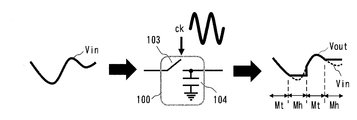
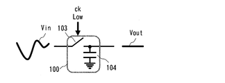
- the operation of the track-and-hold circuit 100 will be described with reference to FIGS. 8A to 8C.
- the simplest operating model of the track-and-hold circuit 100 consists of an analog switch 103 and a capacitor 104.
- the analog switch 103 switches between two states, a track mode Mt that transmits the input as it is to the output, and a hold mode Mh that electrically cuts off the input and the output, according to the High / Low of the clock signal ck.
- the capacitor 104 is used to hold the voltage of the output signal Vout cut off from the input in the hold mode at a constant value.
- the relationship between the clock signal ck and the mode of the track-and-hold circuit 100 may be arbitrarily determined, but in the examples of FIGS. 8A to 8C, when the clock signal ck is High, the track mode Mt is set and the clock signal ck is set. An example in which the hold mode Mh is set when is Low will be described.
- Another reason for using the track and hold circuit in the front end of the ADC is to reduce the effect of noise due to clock jitter. Since the timing of the clock signals is not perfectly evenly spaced, there is statistical variation in the timing of holding the input signal. When there is such clock jitter, it is observed that noise is superimposed on the output of the ADC.
- the clock jitter is within the hold time of the track-and-hold circuit. If so, it will not be affected by noise.
- analog circuits are composed of connecting switching elements called transistors, resistors, capacitors, etc.
- transistors There are several types of transistors, but bipolar transistors are often used in analog circuits that require high-speed operation.
- a switched-emitter follower As a circuit configuration of an existing track-and-hold circuit using a bipolar transistor, what is called a switched-emitter follower is well known.
- FIG. 9 shows a typical configuration of a conventional switched-emitter follower circuit using a bipolar transistor.
- VCS and VEE are power supply voltages
- Vin is an input signal
- Vout is an output signal
- ck + and ck ⁇ are clock signals.
- the clock signals ck + and ck ⁇ are differential signals. Further, (const.) In FIG. 9 indicates that the voltage or current is constant regardless of time.
- the switched emitter follower circuit is composed of bipolar transistors M1 to M3, a capacitor Hold, and a constant current source IS.
- the constant current source IS is often composed of a transistor or the like.
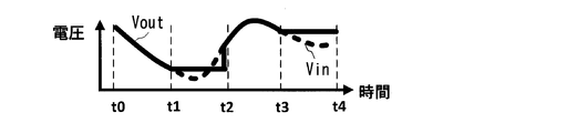
- FIGS. 10A to 10E The basic operation of the switched emitter follower circuit of FIG. 9 will be described with reference to FIGS. 10A to 10E.
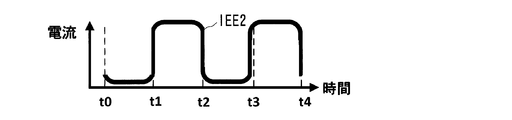
- the waveforms of the currents IEE1 and IEE2 when the differential clock signals ck + and ck ⁇ having a period of Tck shown in FIG. 10A and the input signal Vin shown in FIG. 10B are applied to the switched emitter follower circuit are shown. 10C, FIG. 10D, and the waveform of the output signal Vout is shown in FIG. 10E.
- T0, t1, t2, t3, and t4 in FIGS. 10A to 10E represent the time.
- t0 to t4 are lined up at regular intervals of Tck / 2.
- the output signal Vout is held at a constant value only while the clock signal is Low. .. That is, when the time t satisfies t1 ⁇ t ⁇ t2 or t3 ⁇ t ⁇ t4, the switched emitter follower circuit is in the hold mode.
- the basic operation of the switched-emitter follower circuit is to alternately repeat the track mode and the hold mode according to the high / low of the clock signal.
- the data rate of the switched-emitter follower circuit that is, the number of times data is acquired per unit time, depends on the clock frequency.
- there is an upper limit to the frequency of the clock signal that can be input due to the constraints of the analog circuit, specifically, the parasitic resistance and capacitance existing in the transistor and wiring.
- the upper limit of the frequency of this clock signal is the main factor that limits the speed of the switched emitter follower circuit.
- the present invention has been made to solve the above problems, and an object of the present invention is to provide a switched emitter follower circuit capable of operating at a sampling frequency twice the clock frequency.
- the base is connected to the signal input terminal, the first power supply voltage is applied to the collector, the emitter is connected to the signal output terminal, and one end is described above.
- a capacitor connected to the collector of the first transistor and the other end connected to the emitter of the first transistor, and a positive phase clock output terminal connected to the emitter of the first transistor, and a negative phase clock output terminal
- the multiplication result of the first differential clock signal connected to the base of the first transistor and input from the outside and the second differential clock signal is obtained by the positive phase clock output terminal and the negative phase clock output terminal. It is characterized by including a Gilbert cell type multiplication circuit configured to output to.
- the base is connected to the positive phase signal input terminal, the first power supply voltage is applied to the collector, and the emitter is connected to the positive phase signal output terminal.
- a second transistor in which the base is connected to the negative-phase signal input terminal, the first power supply voltage is applied to the collector, the emitter is connected to the negative-phase signal output terminal, and one end is the first transistor.
- the first capacitor is connected to the collector of the first transistor and the other end is connected to the emitter of the first transistor, and one end is connected to the collector of the second transistor and the other end is connected to the emitter of the second transistor.
- the connected second capacitor and the first positive-phase clock output terminal are connected to the emitter of the first transistor, and the first negative-phase clock output terminal is connected to the base of the first transistor to be external.
- the multiplication result of the first differential clock signal and the second differential clock signal input from is output to the first positive phase clock output terminal and the first negative phase clock output terminal.
- the first Gilbert cell type multiplication circuit and the second positive phase clock output terminal are connected to the emitter of the second transistor, and the second negative phase clock output terminal is connected to the base of the second transistor. Then, the multiplication result of the first differential clock signal and the second differential clock signal is output to the second positive phase clock output terminal and the second negative phase clock output terminal. It is characterized by including a second Gilbert cell type multiplication circuit.
- the sampling frequency of the switched emitter follower circuit is increased to twice the clock frequency while the clock frequency remains the same as before. be able to. Therefore, according to the present invention, it is possible to realize a high-speed switched-emitter follower circuit while keeping the restrictions of the analog circuit as before.
- the clock frequency remains the same as before, and the clock frequency is switched.
- the sampling frequency of the emitter follower circuit can be increased to twice the clock frequency.
- the resistance of the switched emitter follower circuit to the in-phase noise of the input signal can be enhanced by forming the first and second transistors of the input in a differential configuration.
- FIG. 1 is a circuit diagram showing a configuration of a switched emitter follower circuit according to a first embodiment of the present invention.
- FIG. 2 is a circuit diagram showing a typical configuration of a Gilbert cell type multiplication circuit.
- FIG. 3 is a circuit diagram showing a configuration of a switched emitter follower circuit according to a second embodiment of the present invention.
- FIG. 4 is a waveform diagram showing a simulation result of a switched emitter follower circuit according to a second embodiment of the present invention.
- FIG. 5 is a circuit diagram showing a configuration of a switched emitter follower circuit according to a third embodiment of the present invention.
- FIG. 6 is a circuit diagram showing a configuration of a switched emitter follower circuit according to a fourth embodiment of the present invention.
- FIG. 1 is a circuit diagram showing a configuration of a switched emitter follower circuit according to a first embodiment of the present invention.
- FIG. 2 is a circuit diagram showing a typical configuration of a Gilbert cell type multiplication circuit.
- FIG. 7 is a circuit diagram showing an example of a clock distribution circuit of a switched-emitter follower circuit according to a fourth embodiment of the present invention.
- 8A-8C are diagrams illustrating the operation of the track and hold circuit.
- FIG. 9 is a circuit diagram showing the configuration of a conventional switched emitter follower circuit.
- 10A-10E are diagrams showing signal waveforms of each part of a conventional switched emitter follower circuit.
- FIG. 1 is a circuit diagram showing a configuration of a switched emitter follower circuit according to a first embodiment of the present invention.
- the base is connected to the signal input terminal (Vin)
- the power supply voltage VCS is applied to the collector
- the emitter is connected to the signal output terminal (Vout).
- the capacitor Hold one end of which is connected to the collector of the transistor M1 and the other end of which is connected to the emitter of the transistor M1, and the positive phase clock output terminal (outp) are connected to the emitter of the transistor M1.
- the positive phase signal ccp1 of the differential clock signal ck1 is input to the base, the NPN bipolar transistor M4 whose collector is connected to the negative phase clock output terminal (outn), and the differential clock signal to the base.
- the negative phase signal ckn1 of ck1 is input, the NPN bipolar transistor M5 whose collector is connected to the positive phase clock output terminal (outp), and the negative phase signal ckn1 of the differential clock signal ck1 are input to the base, and the collector is negative phase.
- the NPN bipolar transistor M6 connected to the clock output terminal (outn) and the positive phase signal ccp1 of the differential clock signal ck1 are input to the base, and the collector is connected to the positive phase clock output terminal (outp) NPN bipolar transistor M7.
- the positive phase signal ccp2 of the differential clock signal ck2 is input to the base, the NPN bipolar transistor M8 whose collector is connected to the emitters of the transistors M4 and M5, and the negative phase signal ckn2 of the differential clock signal ck2 are input to the base.
- the collector is connected to the emitters of the transistors M6 and M7, and the NPN bipolar transistor M9 is connected to the emitters of the transistors M8 and M9. It is composed of a constant current source IT to be supplied.
- the transistors M4 and M5 form an upper differential pair in which the positive phase signal ccp1 and the negative phase signal ckn1 of the differential clock signal ck1 are input.
- the transistors M6 and M7 form an upper differential pair.
- the transistors M8 and M9 receive the positive phase signal ccp2 and the negative phase signal ckn2 of the differential clock signal ck2 as inputs, and apply a tail current to the upper differential pair composed of the transistors M4 and M5 and the upper differential pair composed of the transistors M6 and M7. Supply.
- the positive phase signal outp of the multiplication result of the differential clock signals ck1 and ck2 is output from the collectors (positive phase clock output terminals) of the transistors M5 and M7, and the difference is obtained from the collectors (negative phase clock output terminals) of the transistors M4 and M6.
- the reverse phase signal outn which is the result of multiplying the dynamic clock signals ck1 and ck2, is output.
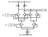
- FIG. 2 A typical configuration of the Gilbert cell type multiplication circuit is shown in FIG. In the configuration of FIG. 2, the load resistor R1 is connected to the reverse-phase clock output terminal, the load resistor R2 is connected to the positive-phase clock output terminal, and the inputs are differential signals in1 and in2, but the operation of the circuit is It is the same as the Gilbert cell type multiplication circuit 10 of FIG.
- the frequencies of the differential clock signals ck1 and ck2 are the same.
- the positive phase signal ccp1 of the differential clock signal ck1 is input to the transistors M4 and M7, and the negative phase signal ckn1 is input to the transistors M5 and M6.
- the input of the signal ckn1 may be reversed.
- the positive phase signal ccp2 of the differential clock signal ck2 is input to the transistor M8, and the negative phase signal ckn2 is input to the transistor M9. good.
- one of the positive phase signal ccp1 and the negative phase signal ckn1 may be a DC bias voltage.
- a single-phase clock signal may be input to one of the pair of transistors M4 and M7 and the set of transistors M5 and M6, and a DC bias voltage may be input to the other set.
- one of the positive phase signal ccp2 and the negative phase signal ckn2 may be a DC bias voltage.
- a single-phase clock signal may be input to one of the transistors M8 and M9, and a DC bias voltage may be input to the other.
- the differential clock signals ck1 and ck2 do not have to be in phase, and there is no problem even if the differential clock signals ck1 and ck2 have a delay (phase difference).
- the load current of the transistor M1 oscillates at the frequency obtained by multiplying the differential clock signals ck1 and ck2, that is, at a frequency twice the clock frequency. Therefore, the transistor M1 switches at a frequency twice the clock frequency.
- the sampling frequency of the switched emitter follower circuit can be doubled of the clock frequency. Therefore, according to this embodiment, the speed of the switched emitter follower circuit can be increased.
- FIG. 3 is a circuit diagram showing a configuration of a switched emitter follower circuit according to a second embodiment of the present invention.
- the base is connected to the positive phase signal input terminal (Vimp)
- the power supply voltage VCS is applied to the collector
- the emitter is connected to the positive phase signal output terminal (Voutp).
- Vinn the negative phase signal input terminal
- Voutn the negative phase signal output terminal
- the positive phase clock output terminal (outpp) of 1 is connected to the emitter of the transistor M1p
- the first negative phase clock output terminal (outnp) is connected to the base of the transistor M1p
- the differential clock signal ck1 and the differential clock signal ck2 The Gilbert cell type multiplication circuit 10p that outputs the multiplication result to the first positive phase clock output terminal and the first negative phase clock output terminal, and the second positive phase clock output terminal (outpn) is the emitter of the transistor M1n.
- the second reverse phase clock output terminal (outnn) is connected to the base of the transistor M1n, and the multiplication result of the differential clock signal ck1 and the differential clock signal ck2 is calculated as the second positive phase clock output terminal and the second positive phase clock output terminal. It is composed of a Gilbert cell type multiplication circuit 10n that outputs to the reverse phase clock output terminal of 2.
- the Gilbert cell type multiplication circuit 10p is different from the NPN bipolar transistor M4p in which the positive phase signal ccp1 of the differential clock signal ck1 is input to the base and the collector is connected to the first negative phase clock output terminal (outnp).
- the reverse phase signal ckn1 of the dynamic clock signal ck1 is input, and the NPN bipolar transistor M5p whose collector is connected to the first positive phase clock output terminal (outpp) and the reverse phase signal ckn1 of the differential clock signal ck1 are input to the base.
- the NPN bipolar transistor M6p in which the collector is connected to the first negative phase clock output terminal (outnp) and the positive phase signal ccp1 of the differential clock signal ck1 are input to the base, and the collector outputs the first positive phase clock.
- the reverse phase signal ckn2 of the differential clock signal ck2 is input, the collector is connected to the emitters of the transistors M6p and M7p, the NPN bipolar transistor M9p, and one end is connected to the emitters of the transistors M8p and M9p, and the power supply voltage VEE is connected to the other end.
- the Gilbert cell type multiplication circuit 10n is different from the NPN bipolar transistor M4n in which the positive phase signal ccp1 of the differential clock signal ck1 is input to the base and the collector is connected to the second negative phase clock output terminal (outnn) and the base.
- the reverse phase signal ckn1 of the dynamic clock signal ck1 is input, and the NPN bipolar transistor M5n whose collector is connected to the second positive phase clock output terminal (outpn) and the reverse phase signal ckn1 of the differential clock signal ck1 are input to the base.
- the NPN bipolar transistor M6n in which the collector is connected to the second negative phase clock output terminal (outnn) and the positive phase signal ccp1 of the differential clock signal ck1 are input to the base, and the collector outputs the second positive phase clock.
- the reverse phase signal ckn2 of the differential clock signal ck2 is input, the collector is connected to the emitters of the transistors M6n and M7n, the NPN bipolar transistor M9n, and one end is connected to the emitters of the transistors M8n and M9n, and the power supply voltage VEE is connected to the other end. Is applied, and is composed of a constant current source ITn that supplies a constant current to the transistors M8n and M9n.
- the operation of the Gilbert cell type multiplication circuits 10p and 10n is the same as that of the Gilbert cell type multiplication circuit 10 of the first embodiment.
- the positive phase signal outpp of the multiplication result of the differential clock signals ck1 and ck2 is output from the collectors (first positive phase clock output terminals) of the transistors M5p and M7p of the Gilbert cell type multiplication circuit 10p, and the collectors of the transistors M4p and M6p (the collectors of the transistors M4p and M6p).
- the reverse phase signal outnp as a result of multiplying the differential clock signals ck1 and ck2 is output from the first reverse phase clock output terminal).
- the positive phase signal outpn of the multiplication result of the differential clock signals ck1 and ck2 is output from the collectors (second positive phase clock output terminals) of the transistors M5n and M7n of the Gilbert cell type multiplication circuit 10n, and the transistors M4n and M6n.
- the reverse-phase signal outnn which is the result of multiplying the differential clock signals ck1 and ck2, is output from the collector (second reverse-phase clock output terminal) of.
- the input signal has a differential configuration (Vimp, Vinn), and the input transistor has a differential configuration of M1p, M1n accordingly, so that the switched emitter follower with respect to the in-phase noise of the input signal
- the resistance of the circuit can be enhanced.
- the positive phase signal Vinp and the negative phase signal Vinn of the differential input signal were set to a sine wave having a frequency of 200 Hz, and the amplitude was set to 100 mV.
- the positive phase signal ccp1 and the negative phase signal ckn1 of the differential clock signal ck1 were set to a sine wave having a frequency of 1 kHz, and the amplitude was set to 100 mV.
- the differential clock signal ck2 the same signal as the differential clock signal ck1 was used.
- the capacities of the capacitors Holdp and Holdn were set to 500 nF, and the current flowing through the constant current sources ITp and ITn was set to 1 mA.
- FIG. 4 The result of simulating the response of the switched emitter follower circuit of FIG. 3 over a time of 10 ms is shown in FIG. According to FIG. 4, it can be seen that sampling is performed at 2 kHz, which is twice that of the clock frequency of 1 kHz, as expected.
- FIG. 5 is a circuit diagram showing a configuration of a switched emitter follower circuit according to a third embodiment of the present invention.
- the switched-emitter follower circuit of this embodiment is composed of NPN bipolar transistors M1p, M1n, capacitors Choldp, and Coldn, and Gilbert cell type multiplication circuits 10p, 10n'.
- the second embodiment has a configuration in which two Gilbert cell type multiplication circuits 10p and 10n of the same type as the Gilbert cell type multiplication circuit 10 of the first embodiment are provided. Since the lower movable pair (M8p, M9p) of the Gilbert cell type multiplication circuit 10p and the lower movable pair (M8n, M9n) of the Gilbert cell type multiplication circuit 10n operate exactly the same, they are used together. It is possible to reduce the number of transistors.
- the configuration of the Gilbert cell type multiplication circuit 10p is the same as that in the second embodiment.
- the configuration of the upper differential pair composed of the transistors M4n and M5n of the Gilbert cell type multiplication circuit 10n'and the upper differential pair composed of the transistors M6n and M7n is the same as that of the Gilbert cell type multiplication circuit 10n.
- the Gilbert cell type multiplication circuit 10n' is designed to share the current source circuit with the Gilbert cell type multiplication circuit 10p. Specifically, the emitters of the transistors M4n and M5n of the Gilbert cell type multiplication circuit 10n'are connected to the collector of the transistor M8p, and the emitters of the transistors M6n and M7n are connected to the collector of the transistor M9p.
- the number of transistors can be reduced as compared with the second embodiment, so that the circuit scale can be reduced and the power consumption can be reduced.
- FIG. 6 is a circuit diagram showing a configuration of a switched emitter follower circuit according to a fourth embodiment of the present invention.
- the NPN bipolar transistor M1 the capacitor Hold
- the Gilbert cell type multiplication circuit 10 the differential clock signal ck are the differential clock signal ck1 and the differential clock signal ck2. It is composed of a clock distribution circuit 11 that branches into one.
- the differential clock signals ck1 and ck2 are input to the switched emitter follower circuit from the outside.
- the differential clock signals ck1 and ck2 are generated by branching the differential clock signal ck by the clock distribution circuit 11. Thereby, in this embodiment, the differential clock signal applied from the outside can be unified.
- FIG. 7 shows an example of a specific configuration of the clock distribution circuit 11.
- the clock distribution circuit 11 includes an NPN bipolar transistor M10 in which the positive phase signal ccp of the differential clock signal ck is input to the base, and an NPN bipolar transistor M11 in which the negative phase signal ckn of the differential clock signal ck is input to the base.
- NPN bipolar transistor M12 in which the power supply voltage VCS is applied to the base and collector and the emitter is connected to the collector of transistor M10, and NPN bipolar transistor M12 in which the power supply voltage VCS is applied to the base and collector and the emitter is connected to the collector of transistor M11.
- the transistor M13 one end is connected to the emitter of the transistor M10, and the constant current source IT10 to which the power supply voltage VEE is applied to the other end, and one end is connected to the emitter of the transistor M11 and the power supply voltage VEE is applied to the other end. It is composed of a constant current source IT11.
- the configuration of FIG. 7 uses an emitter follower circuit.
- the differential clock signal ck is output as it is as the differential clock signal ck1.
- a signal obtained by shifting the bias voltage of the positive phase signal ccp of the differential clock signal ck by the base-emitter voltage of the transistor M10 is output from the emitter of the transistor M10 as the positive phase signal ccp2 of the differential clock signal ck2.
- NS a signal obtained by shifting the bias voltage of the reverse phase signal ckn of the differential clock signal ck by the base-emitter voltage of the transistor M11 is output from the emitter of the transistor M11 as the reverse phase signal ckn2 of the differential clock signal ck2.
- the configuration of the clock distribution circuit 11 is not limited to FIG. 7, and other configurations may be used. Further, in the examples of FIGS. 6 and 7, the clock distribution circuit 11 is applied to the first embodiment, but the clock distribution circuit 11 is applied to the second and third embodiments. Needless to say, it's okay.
- the present invention can be applied to a switched emitter follower circuit.
- M1, M4 to M9, M1p, M4p to M9p, M1n, M4n to M9n NPN bipolar transistors, IT, ITp, ITn ... constant current sources, Hold, Holdp, Clockn ... capacitors, 10,10p, 10n, 10n'... Gilbert Cell type multiplication circuit, 11 ... Clock distribution circuit.
Landscapes
- Engineering & Computer Science (AREA)
- Theoretical Computer Science (AREA)
- Power Engineering (AREA)
- Amplifiers (AREA)
- Analogue/Digital Conversion (AREA)
- Electronic Switches (AREA)
Priority Applications (3)
| Application Number | Priority Date | Filing Date | Title |
|---|---|---|---|
| US17/917,185 US11764800B2 (en) | 2020-04-09 | 2020-04-09 | Switched emitter follower circuit |
| PCT/JP2020/015940 WO2021205592A1 (ja) | 2020-04-09 | 2020-04-09 | スイッチト・エミッタ・フォロワ回路 |
| JP2022513792A JP7375916B2 (ja) | 2020-04-09 | 2020-04-09 | スイッチト・エミッタ・フォロワ回路 |
Applications Claiming Priority (1)
| Application Number | Priority Date | Filing Date | Title |
|---|---|---|---|
| PCT/JP2020/015940 WO2021205592A1 (ja) | 2020-04-09 | 2020-04-09 | スイッチト・エミッタ・フォロワ回路 |
Publications (1)
| Publication Number | Publication Date |
|---|---|
| WO2021205592A1 true WO2021205592A1 (ja) | 2021-10-14 |
Family
ID=78023929
Family Applications (1)
| Application Number | Title | Priority Date | Filing Date |
|---|---|---|---|
| PCT/JP2020/015940 Ceased WO2021205592A1 (ja) | 2020-04-09 | 2020-04-09 | スイッチト・エミッタ・フォロワ回路 |
Country Status (3)
| Country | Link |
|---|---|
| US (1) | US11764800B2 (https=) |
| JP (1) | JP7375916B2 (https=) |
| WO (1) | WO2021205592A1 (https=) |
Citations (4)
| Publication number | Priority date | Publication date | Assignee | Title |
|---|---|---|---|---|
| JP2011061278A (ja) * | 2009-09-07 | 2011-03-24 | Yokogawa Electric Corp | スイッチトエミッタフォロワ回路 |
| JP2013055444A (ja) * | 2011-09-02 | 2013-03-21 | Asahi Kasei Electronics Co Ltd | 位相検出回路及び検査方法 |
| JP2018121137A (ja) * | 2017-01-24 | 2018-08-02 | アール・エフ・アーキテクチャ株式会社 | 乗算器 |
| JP2019179978A (ja) * | 2018-03-30 | 2019-10-17 | 日本電信電話株式会社 | トラック・アンド・ホールド回路 |
Family Cites Families (2)
| Publication number | Priority date | Publication date | Assignee | Title |
|---|---|---|---|---|
| US4575647A (en) * | 1983-07-08 | 1986-03-11 | International Business Machines Corporation | Reference-regulated compensated current switch emitter-follower circuit |
| US11830560B2 (en) * | 2020-01-28 | 2023-11-28 | Nippon Telegraph And Telephone Corporation | Track-and-hold circuit |
-
2020
- 2020-04-09 WO PCT/JP2020/015940 patent/WO2021205592A1/ja not_active Ceased
- 2020-04-09 JP JP2022513792A patent/JP7375916B2/ja active Active
- 2020-04-09 US US17/917,185 patent/US11764800B2/en active Active
Patent Citations (4)
| Publication number | Priority date | Publication date | Assignee | Title |
|---|---|---|---|---|
| JP2011061278A (ja) * | 2009-09-07 | 2011-03-24 | Yokogawa Electric Corp | スイッチトエミッタフォロワ回路 |
| JP2013055444A (ja) * | 2011-09-02 | 2013-03-21 | Asahi Kasei Electronics Co Ltd | 位相検出回路及び検査方法 |
| JP2018121137A (ja) * | 2017-01-24 | 2018-08-02 | アール・エフ・アーキテクチャ株式会社 | 乗算器 |
| JP2019179978A (ja) * | 2018-03-30 | 2019-10-17 | 日本電信電話株式会社 | トラック・アンド・ホールド回路 |
Also Published As
| Publication number | Publication date |
|---|---|
| JP7375916B2 (ja) | 2023-11-08 |
| JPWO2021205592A1 (https=) | 2021-10-14 |
| US11764800B2 (en) | 2023-09-19 |
| US20230141476A1 (en) | 2023-05-11 |
Similar Documents
| Publication | Publication Date | Title |
|---|---|---|
| US8089388B2 (en) | Folding analog-to-digital converter | |
| US12081178B2 (en) | Amplifier with VCO-based ADC | |
| CN105049043A (zh) | 一种带有失调校正功能的高速比较器 | |
| CN108649951A (zh) | 一种具有相位自动调节功能的两相时钟信号产生电路 | |
| TW200952325A (en) | High speed differential to single ended converting circuit | |
| CN114374388B (zh) | 一种两步式建立的自举采样开关电路及集成电路 | |
| US5157276A (en) | Low jitter clock phase adjust system | |
| CN101512906B (zh) | 折叠电路和模数转换器 | |
| WO2020057370A1 (zh) | 一种双路时钟信号转脉宽调制信号电路 | |
| JP2004312555A (ja) | コンパレータ、差動増幅器、2段増幅器及びアナログ/ディジタル変換器 | |
| Razavi et al. | A 200 MHz 15 mW BiCMOS sample-and-hold amplifier with 3 V supply | |
| US11362669B2 (en) | Track and hold circuit | |
| CN207706157U (zh) | 用于采样保持器的四相25%占空比时钟发生电路 | |
| JP7331956B2 (ja) | トラック・アンド・ホールド回路 | |
| JP7375916B2 (ja) | スイッチト・エミッタ・フォロワ回路 | |
| US7479915B1 (en) | Comparator architecture | |
| EP2323256B1 (en) | Method and system for improving limiting amplifier phase noise for low slew-rate input signals | |
| JP7444244B2 (ja) | トラック・アンド・ホールド回路 | |
| Boni et al. | 3.3-V, 200-Ms/s BiCMOS comparator for current-mode interpolation using a transconductance stage | |
| Lin et al. | A 1.8 V low-power CMOS high-speed four quadrant multiplier with rail-to-rail differential input | |
| Edwards et al. | A Laddered-Inverter Nonoverlapping Clock Generator | |
| WO2026003918A1 (ja) | トラック・アンド・ホールド回路 | |
| Hiremath et al. | A 6-bit low power folding and interpolating ADC | |
| Jain et al. | Design and Simulation of Two Stage Sample and Hold Circuit with Low Power using Current Controlled Conveyor | |
| US20210111709A1 (en) | Methods and system for a resettable flip flop |
Legal Events
| Date | Code | Title | Description |
|---|---|---|---|
| 121 | Ep: the epo has been informed by wipo that ep was designated in this application |
Ref document number: 20930359 Country of ref document: EP Kind code of ref document: A1 |
|
| ENP | Entry into the national phase |
Ref document number: 2022513792 Country of ref document: JP Kind code of ref document: A |
|
| NENP | Non-entry into the national phase |
Ref country code: DE |
|
| 122 | Ep: pct application non-entry in european phase |
Ref document number: 20930359 Country of ref document: EP Kind code of ref document: A1 |