WO2021200994A1 - 2次元フォトニック結晶レーザ - Google Patents
2次元フォトニック結晶レーザ Download PDFInfo
- Publication number
- WO2021200994A1 WO2021200994A1 PCT/JP2021/013620 JP2021013620W WO2021200994A1 WO 2021200994 A1 WO2021200994 A1 WO 2021200994A1 JP 2021013620 W JP2021013620 W JP 2021013620W WO 2021200994 A1 WO2021200994 A1 WO 2021200994A1
- Authority
- WO
- WIPO (PCT)
- Prior art keywords
- photonic crystal
- dimensional photonic
- electrode
- partial
- refractive index
- Prior art date
- Legal status (The legal status is an assumption and is not a legal conclusion. Google has not performed a legal analysis and makes no representation as to the accuracy of the status listed.)
- Ceased
Links
Images




Classifications
-
- H—ELECTRICITY
- H01—ELECTRIC ELEMENTS
- H01S—DEVICES USING THE PROCESS OF LIGHT AMPLIFICATION BY STIMULATED EMISSION OF RADIATION [LASER] TO AMPLIFY OR GENERATE LIGHT; DEVICES USING STIMULATED EMISSION OF ELECTROMAGNETIC RADIATION IN WAVE RANGES OTHER THAN OPTICAL
- H01S5/00—Semiconductor lasers
- H01S5/10—Construction or shape of the optical resonator, e.g. extended or external cavity, coupled cavities, bent-guide, varying width, thickness or composition of the active region
- H01S5/11—Comprising a photonic bandgap structure
-
- H—ELECTRICITY
- H01—ELECTRIC ELEMENTS
- H01S—DEVICES USING THE PROCESS OF LIGHT AMPLIFICATION BY STIMULATED EMISSION OF RADIATION [LASER] TO AMPLIFY OR GENERATE LIGHT; DEVICES USING STIMULATED EMISSION OF ELECTROMAGNETIC RADIATION IN WAVE RANGES OTHER THAN OPTICAL
- H01S5/00—Semiconductor lasers
- H01S5/04—Processes or apparatus for excitation, e.g. pumping, e.g. by electron beams
- H01S5/042—Electrical excitation ; Circuits therefor
- H01S5/0425—Electrodes, e.g. characterised by the structure
- H01S5/04254—Electrodes, e.g. characterised by the structure characterised by the shape
-
- H—ELECTRICITY
- H01—ELECTRIC ELEMENTS
- H01S—DEVICES USING THE PROCESS OF LIGHT AMPLIFICATION BY STIMULATED EMISSION OF RADIATION [LASER] TO AMPLIFY OR GENERATE LIGHT; DEVICES USING STIMULATED EMISSION OF ELECTROMAGNETIC RADIATION IN WAVE RANGES OTHER THAN OPTICAL
- H01S5/00—Semiconductor lasers
- H01S5/04—Processes or apparatus for excitation, e.g. pumping, e.g. by electron beams
- H01S5/042—Electrical excitation ; Circuits therefor
- H01S5/0425—Electrodes, e.g. characterised by the structure
- H01S5/04256—Electrodes, e.g. characterised by the structure characterised by the configuration
-
- H—ELECTRICITY
- H01—ELECTRIC ELEMENTS
- H01S—DEVICES USING THE PROCESS OF LIGHT AMPLIFICATION BY STIMULATED EMISSION OF RADIATION [LASER] TO AMPLIFY OR GENERATE LIGHT; DEVICES USING STIMULATED EMISSION OF ELECTROMAGNETIC RADIATION IN WAVE RANGES OTHER THAN OPTICAL
- H01S5/00—Semiconductor lasers
- H01S5/06—Arrangements for controlling the laser output parameters, e.g. by operating on the active medium
- H01S5/062—Arrangements for controlling the laser output parameters, e.g. by operating on the active medium by varying the potential of the electrodes
- H01S5/06233—Controlling other output parameters than intensity or frequency
- H01S5/06243—Controlling other output parameters than intensity or frequency controlling the position or direction of the emitted beam
-
- H—ELECTRICITY
- H01—ELECTRIC ELEMENTS
- H01S—DEVICES USING THE PROCESS OF LIGHT AMPLIFICATION BY STIMULATED EMISSION OF RADIATION [LASER] TO AMPLIFY OR GENERATE LIGHT; DEVICES USING STIMULATED EMISSION OF ELECTROMAGNETIC RADIATION IN WAVE RANGES OTHER THAN OPTICAL
- H01S5/00—Semiconductor lasers
- H01S5/10—Construction or shape of the optical resonator, e.g. extended or external cavity, coupled cavities, bent-guide, varying width, thickness or composition of the active region
- H01S5/18—Surface-emitting [SE] lasers, e.g. having both horizontal and vertical cavities
- H01S5/185—Surface-emitting [SE] lasers, e.g. having both horizontal and vertical cavities having only horizontal cavities, e.g. horizontal cavity surface-emitting lasers [HCSEL]
-
- H—ELECTRICITY
- H01—ELECTRIC ELEMENTS
- H01S—DEVICES USING THE PROCESS OF LIGHT AMPLIFICATION BY STIMULATED EMISSION OF RADIATION [LASER] TO AMPLIFY OR GENERATE LIGHT; DEVICES USING STIMULATED EMISSION OF ELECTROMAGNETIC RADIATION IN WAVE RANGES OTHER THAN OPTICAL
- H01S5/00—Semiconductor lasers
- H01S5/30—Structure or shape of the active region; Materials used for the active region
- H01S5/34—Structure or shape of the active region; Materials used for the active region comprising quantum well or superlattice structures, e.g. single quantum well [SQW] lasers, multiple quantum well [MQW] lasers or graded index separate confinement heterostructure [GRINSCH] lasers
- H01S5/343—Structure or shape of the active region; Materials used for the active region comprising quantum well or superlattice structures, e.g. single quantum well [SQW] lasers, multiple quantum well [MQW] lasers or graded index separate confinement heterostructure [GRINSCH] lasers in AIIIBV compounds, e.g. AlGaAs-laser, InP-based laser
- H01S5/34313—Structure or shape of the active region; Materials used for the active region comprising quantum well or superlattice structures, e.g. single quantum well [SQW] lasers, multiple quantum well [MQW] lasers or graded index separate confinement heterostructure [GRINSCH] lasers in AIIIBV compounds, e.g. AlGaAs-laser, InP-based laser with a well layer having only As as V-compound, e.g. AlGaAs, InGaAs
-
- H—ELECTRICITY
- H01—ELECTRIC ELEMENTS
- H01S—DEVICES USING THE PROCESS OF LIGHT AMPLIFICATION BY STIMULATED EMISSION OF RADIATION [LASER] TO AMPLIFY OR GENERATE LIGHT; DEVICES USING STIMULATED EMISSION OF ELECTROMAGNETIC RADIATION IN WAVE RANGES OTHER THAN OPTICAL
- H01S2301/00—Functional characteristics
- H01S2301/18—Semiconductor lasers with special structural design for influencing the near- or far-field
-
- H—ELECTRICITY
- H01—ELECTRIC ELEMENTS
- H01S—DEVICES USING THE PROCESS OF LIGHT AMPLIFICATION BY STIMULATED EMISSION OF RADIATION [LASER] TO AMPLIFY OR GENERATE LIGHT; DEVICES USING STIMULATED EMISSION OF ELECTROMAGNETIC RADIATION IN WAVE RANGES OTHER THAN OPTICAL
- H01S5/00—Semiconductor lasers
- H01S5/02—Structural details or components not essential to laser action
- H01S5/026—Monolithically integrated components, e.g. waveguides, monitoring photo-detectors, drivers
- H01S5/0267—Integrated focusing lens
-
- H—ELECTRICITY
- H01—ELECTRIC ELEMENTS
- H01S—DEVICES USING THE PROCESS OF LIGHT AMPLIFICATION BY STIMULATED EMISSION OF RADIATION [LASER] TO AMPLIFY OR GENERATE LIGHT; DEVICES USING STIMULATED EMISSION OF ELECTROMAGNETIC RADIATION IN WAVE RANGES OTHER THAN OPTICAL
- H01S5/00—Semiconductor lasers
- H01S5/06—Arrangements for controlling the laser output parameters, e.g. by operating on the active medium
- H01S5/062—Arrangements for controlling the laser output parameters, e.g. by operating on the active medium by varying the potential of the electrodes
- H01S5/06233—Controlling other output parameters than intensity or frequency
- H01S5/0624—Controlling other output parameters than intensity or frequency controlling the near- or far field
-
- H—ELECTRICITY
- H01—ELECTRIC ELEMENTS
- H01S—DEVICES USING THE PROCESS OF LIGHT AMPLIFICATION BY STIMULATED EMISSION OF RADIATION [LASER] TO AMPLIFY OR GENERATE LIGHT; DEVICES USING STIMULATED EMISSION OF ELECTROMAGNETIC RADIATION IN WAVE RANGES OTHER THAN OPTICAL
- H01S5/00—Semiconductor lasers
- H01S5/20—Structure or shape of the semiconductor body to guide the optical wave ; Confining structures perpendicular to the optical axis, e.g. index or gain guiding, stripe geometry, broad area lasers, gain tailoring, transverse or lateral reflectors, special cladding structures, MQW barrier reflection layers
- H01S5/2004—Confining in the direction perpendicular to the layer structure
- H01S5/2018—Optical confinement, e.g. absorbing-, reflecting- or waveguide-layers
- H01S5/2027—Reflecting region or layer, parallel to the active layer, e.g. to modify propagation of the mode in the laser or to influence transverse modes
Definitions
- the present invention relates to a two-dimensional photonic crystal laser that amplifies light using a two-dimensional photonic crystal.
- the two-dimensional photonic crystal laser includes an active layer, a two-dimensional photonic crystal layer, and a pair of electrodes provided so as to sandwich them.
- the active layer causes light emission in a specific emission wavelength band by injecting carriers (holes, electrons) from the electrodes.
- the two-dimensional photonic crystal layer has a structure in which different refractive index regions having different refractive indexes are periodically arranged two-dimensionally on a plate-shaped base material.
- the different refractive index region is composed of pores (air) formed in the base material or a member different from the material of the base material.
- first electrode one electrode
- second electrode a two-dimensional photonic crystal layer and the other electrode
- Patent Documents 1 and 2 describe a two-dimensional photonic crystal laser in which the emission direction of the laser beam is variable (hereinafter, referred to as "two-dimensional photonic crystal laser with variable emission direction").
- a variable emission direction two-dimensional photonic crystal laser is a light source that can be suitably used for forming characters and figures by scanning a laser beam in a laser printer, a laser display, or the like.
- the second electrode is the surface of the second clad layer (opposite to the two-dimensional photonic crystal layer). It is divided into a plurality of electrodes (on the side surface), and a gap is provided between each of the divided electrodes (individual electrodes are referred to as "partial electrodes"). Further, a lens is provided so as to face the surface of the second clad layer. The first electrode is provided so as to cover the entire surface of the first clad layer (the surface opposite to the active layer).
- a part of the active layer (hereinafter, "current") is formed by passing a current between one of the plurality of partial electrodes or the adjacent plurality of the first electrode and the first electrode.
- a current is injected into the "injection region"), and light is generated in the current injection region.
- the laser oscillates in the region of the two-dimensional photonic crystal layer corresponding to the current injection region, and the laser beam is emitted from the two-dimensional photonic crystal layer in the direction perpendicular to the layer.
- the laser beam emitted from the two-dimensional photonic crystal layer is emitted to the outside between the partial electrodes and through the lens.
- the traveling direction of the laser beam emitted to the outside is the position of entering the lens and the current injection that is the basis for determining the position. It depends on the position of the area. Therefore, the traveling direction of the laser beam can be changed by changing the partial electrode to which the current is supplied to change the position of the current injection region, whereby the laser beam can be scanned.
- the different refractive index region is a two-dimensional lattice such as a square lattice or a rectangular lattice. It is located at a position deviated from the grid point of. The deviation of the position of the different refractive index region from the lattice point at each lattice point is defined by a parameter called modulation phase.
- the different refractive index regions are shifted in the directions of different azimuths at the same distance at each lattice point, and the phase of these azimuths corresponds to the modulation phase.
- the two-dimensional photonic crystal layer is virtually divided into a plurality of oscillation regions, and within the same oscillation region, the phase difference of the azimuth angle (phase difference of the modulation phase) between adjacent lattice points has the same value.
- the phase difference has different values between different oscillation regions.
- the second electrode is a partial electrode provided one by one corresponding to each of the plurality of oscillation regions.
- the first electrode is a transparent electrode provided so as to cover the entire surface of the first clad layer, and a laser beam is emitted from the first electrode side. In the second conventional example, the lens is not provided.
- the second conventional example by supplying a current between one of the plurality of partial electrodes and the first electrode, a region corresponding to the one partial electrode of the active layer (current injection). Light is generated in the region), and laser oscillation is performed in the region (oscillation region) of the two-dimensional photonic crystal layer corresponding to the one partial electrode.
- the laser beam travels from a direction perpendicular to the two-dimensional photonic crystal layer in a direction inclined by an inclination angle determined by the modulation phase. Therefore, the modulation phase can be changed by changing the partial electrode to which the current is supplied to change the oscillation region, and the traveling direction of the laser beam can be changed, whereby the laser beam can be scanned.
- the laser beam is emitted to the outside only between the partial electrodes, and a part of the laser beam is blocked by the partial electrodes. Further, in the second conventional example, the laser beam passes through the transparent electrode and is emitted to the outside, but since the light transmittance of the transparent electrode is generally not 100%, the laser beam is attenuated by the transparent electrode. ..
- the problem to be solved by the present invention is to provide a two-dimensional photonic crystal laser having a variable emission direction capable of scanning the laser beam and emitting the laser beam without being attenuated by electrodes. be.
- the active layer and the plate-shaped base material have a two-dimensional periodic cycle of different refractive index regions having different refractive indexes from the base material.
- a two-dimensional photonic crystal laser in which a laminate having a two-dimensional photonic crystal layer arranged in a sword is sandwiched between a first electrode and a second electrode.
- the first electrode is divided into a plurality of partial electrodes.
- the second electrode has a frame-shaped portion made of a conductor, and the window portion, which is a space inside the frame-shaped portion, is arranged so as to face a region surrounding the plurality of partial electrodes.
- a lens provided so as to cover the window portion is provided on the side of the second electrode opposite to the laminated body or on the surface of the laminated body on the second electrode side.
- one of the plurality of partial electrodes constituting the first electrode or a plurality of adjacent electrodes (the region in which these exist is referred to as a "current supply region") and the first.
- a current is injected into the current injection region, which is a region corresponding to the current supply region in the active layer, and light is generated in the current injection region.
- the traveling direction of the laser beam emitted to the outside is the position where the laser beam enters the lens and the current supply which is the basis for determining the position. It depends on the position of the area. Therefore, by changing the position of the current injection region by changing the partial electrode to which the current is supplied, the traveling direction of the laser beam can also be changed, whereby the laser beam can be scanned.
- the lens may be provided on the side opposite to the laminated body of the second electrode, or may be provided on the surface of the laminated body on the second electrode side.
- the lens is integrally formed with the laminated body. This makes it possible to reduce the size of the two-dimensional photonic crystal laser.
- Such a lens integrated with the laminated body can be manufactured by processing the surface of the laminated body on the second electrode side by a method such as etching.
- the current injection region in the active layer is not the same size as the current supply region in the first electrode.
- the window portion of the second electrode is arranged so as to face the region surrounding the plurality of partial electrodes, the outer shape of the frame-shaped portion of the second electrode is larger than the current supply region of the first electrode. Therefore, the current flows from the first electrode to the second electrode so as to spread in the in-plane direction of the active layer. Therefore, the current injection region becomes larger than the current supply region.
- the laser beam emitted from the two-dimensional photonic crystal layer passes through the window portion of the second electrode, that is, the space inside the frame-shaped portion where no conductor exists. Therefore, the laser beam can be emitted without being attenuated.
- the partial current injection region which is a region in which a current is injected into the active layer from each of the plurality of partial electrodes, is formed from the partial electrode adjacent to the partial electrode to the active layer. It is desirable that the distance between the adjacent partial electrodes is set so as to overlap a part of the partial current injection region into which the current is injected. As a result, one undivided current injection region is formed in the active layer, and the light emission from this one current injection region is amplified by the two-dimensional photonic crystal layer to obtain a coherent laser beam. be able to.
- the distance between the first electrode (partial electrode) and the active layer and the distance between the active layer and the second electrode can be achieved so that the partial current injection regions formed by the adjacent partial electrodes overlap each other. It can be realized by setting parameters such as the distance between the two electrodes, the distance between the partial electrodes, and the area of the second electrode.
- the lens is arranged away from the two-dimensional photonic crystal layer by a distance of 0.5 to 2 times the focal length of the lens.
- the two-dimensional photonic crystal layer is The different refractive index region has two partial different refractive index regions, The coupling coefficient ⁇ 180 of the 180 ° diffracted light in which the light propagating in the two-dimensional photonic crystal layer is diffracted in the 180 ° direction by the different refraction region, and the 90 ° diffracted light diffracted in the 90 ° direction.
- the two partial different diffraction regions so that the absolute value of the difference between the coupling coefficients - ⁇ 90 (
- the coupling coefficient is a parameter indicating the intensity of diffracted light, and can be either positive or negative.
- ⁇ 180 is a one-dimensional coupling that represents the interaction between an in-plane waveguide light that is waveguide in one direction and an in-plane waveguide light that is reflected in a different refractive index region and whose traveling direction changes by 180 ° (180 ° diffraction). It is a coefficient (hermeat component).
- ⁇ 90 is a two-dimensional coupling coefficient that represents the interaction between in-plane waveguide light that is guided in one direction and light whose traveling direction is changed by 90 ° depending on the different refractive index region. These ⁇ 180 and ⁇ 90 are determined based on the shape of the different refractive index region.
- a laser beam made of an electrically insulating material is further provided between the plurality of partial electrodes (gap between adjacent partial electrodes). It is desirable to have a reflecting part that reflects. As a result, the laser beam emitted from the two-dimensional photonic crystal layer to the first electrode side is reflected by the reflecting portion and the partial electrode and emitted from the window portion of the second electrode, so that the luminous efficiency can be increased.
- an active layer and a two-dimensional photonic crystal layer in which different refractive index regions having different refractive indexes from the base material are two-dimensionally arranged on a plate-shaped base material are provided.
- the first electrode is divided into a plurality of partial electrodes.
- the second electrode has a frame-shaped portion made of a conductor, and the window portion, which is a space inside the frame-shaped portion, is arranged so as to face a region surrounding the plurality of partial electrodes.
- the two-dimensional photonic crystal layer has a period defined so that the different refractive index region forms a resonance state of a predetermined wavelength by forming a two-dimensional standing wave and does not emit light of that wavelength to the outside. It is arranged by being modulated with a predetermined modulation phase ⁇ at each lattice point of the basic two-dimensional lattice having the property.
- (sin ⁇ sin ⁇ ) / n eff ) and the position vector r ⁇ of each lattice point are used to express ⁇ r ⁇ ⁇ G' ⁇ .
- the angle ⁇ is different depending on the position in the two-dimensional photonic crystal layer.
- one of the plurality of partial electrodes constituting the first electrode or a plurality of adjacent electrodes (the region in which they exist is referred to as "current" as in the first aspect.
- a current By passing a current between the “supply region") and the second electrode, a current is injected into a current injection region, which is a part of the active layer, and light is generated in the current injection region.
- laser oscillation is generated by the light of the predetermined wavelength in the region corresponding to the current injection region (referred to as “optical amplification region”) in the two-dimensional photonic crystal layer, and a laser beam is generated.
- the predetermined wavelength may be included in the wavelength range of the light generated in the active layer.
- the laser beam generated in this way is a two-dimensional photo with an inclination angle (angle formed by the normal line with respect to the two-dimensional photonic crystal layer and the traveling direction of the laser beam) according to the modulation phase of the two-dimensional photonic crystal layer in the photoamplification region. It is emitted from the nick crystal layer, passes through the window portion of the second electrode, and is emitted to the outside of the two-dimensional photonic crystal laser. This tilt angle is determined by the modulation phase ⁇ at each lattice point in the optical amplification region. Since the angle ⁇ that defines the modulation phase differs depending on the position in the two-dimensional photonic crystal layer, the laser can be changed by changing the position of the current injection region by changing the partial electrode into which the current is injected. The traveling direction of the beam can also be changed. Therefore, the laser beam can be scanned.
- the lattice vector G' ⁇ may be defined as a function G'(x, y) ⁇ that depends on the position in the two-dimensional photonic crystal layer. In this case, as shown below, the laser beam to be emitted from the position (x, y) in the two-dimensional photonic crystal layer (strictly speaking, the "in-phase position" of the two-dimensional photonic crystal layer).
- G' ⁇ (x, y) is defined using the tilt angle ⁇ (x, y) and the azimuth angle ⁇ (x, y), and the modulation phase ⁇ (x, y) at the position (x, y) is defined. can do.
- modulation phase ⁇ (x, y) is ... (1) It is represented by.
- This modulation phase ⁇ (x, y) is defined by the inclination angle ⁇ (x, y) and the azimuth angle ⁇ (x, y) at the position (x, y).
- Optical amplification by arranging each different refractive index region in the two-dimensional photonic crystal layer at each lattice point of the basic two-dimensional lattice by modulating it with the modulation phase ⁇ (x, y) shown in Eq. (1).
- a laser beam having an inclination angle ⁇ (x, y) and an inclination angle close to the azimuth angle ⁇ (x, y) that defines the modulation phase of the two-dimensional photonic crystal layer in the region can be obtained.
- the optical amplification region can be said to be the same.
- a laser beam having an inclination angle ⁇ (x, y) and an azimuth angle ⁇ (x, y) can be obtained.
- the laser beam emitted from the two-dimensional photonic crystal layer passes through the window portion of the second electrode, that is, the space inside the frame-shaped portion where no conductor exists. Therefore, the laser beam can be emitted without being attenuated.
- the different refractive index regions are arranged at each lattice point by the same distance from the lattice points, and the angle formed by the direction of the deviation and the reference line is It is possible to take a configuration in which the modulation phase is set for each lattice point due to the difference.
- the different refractive index regions are arranged at each lattice point so as to be offset in the same direction from the lattice points, and each lattice point is displaced due to the difference in the deviation distance. It is also possible to take a configuration in which the modulation phase is set. Here, a direction that differs by 180 ° with respect to a certain direction corresponds to the "same direction" as the certain direction.
- the different refractive index regions are arranged at each lattice point, and the modulation for each lattice point due to the difference in the area of each different refractive index region. It is also possible to take the configuration that the phase is set.
- the partial current injection region which is the region in which the current is injected into the active layer from each of the plurality of partial electrodes, is the said. It is desirable that the distance between the adjacent partial electrodes is set so as to overlap a part of the partial current injection region in which the current is injected into the active layer from the partial electrode adjacent to the partial electrode.
- the two-dimensional photonic crystal laser of the second aspect as in the case of the first aspect, further, electrically between the plurality of partial electrodes (gap between adjacent partial electrodes). It is desirable that the material is made of an insulating material and has a reflecting portion that reflects the laser beam.
- a two-dimensional photonic crystal laser having a variable emission direction capable of scanning the laser beam and emitting the laser beam without being attenuated by the electrodes.
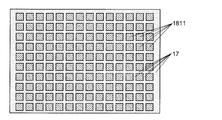
- FIG. 5 is a plan view showing an example of the shape and arrangement of the partial electrodes constituting the first electrode in the two-dimensional photonic crystal laser of the first embodiment.
- FIG. 5 is a plan view showing another example of the shape and arrangement of the partial electrodes constituting the first electrode in the two-dimensional photonic crystal laser of the first embodiment.
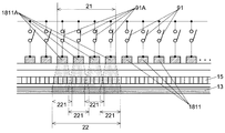
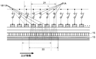
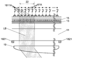
- the figure which shows the example which the current injection region moves by changing the partial electrode which injects a current in the 2D photonic crystal laser of 1st Embodiment.
- FIG. 5 is a diagram showing an example in which a plurality of current injection regions are formed when a current is injected into an active layer from a plurality of adjacent partial electrodes in the two-dimensional photonic crystal laser of the first embodiment.
- the figure for demonstrating the calculation condition for determining the spacing of partial electrodes in the 2D photonic crystal laser of 1st Embodiment In the two-dimensional photonic crystal laser of the first embodiment, the ratio of the distance w from the end of the partial electrode to the current density i 1 / i 0 for each of the cases where the depth d from the partial electrode takes a plurality of values. A graph showing the result of calculating the relationship between. In the two-dimensional photonic crystal laser of the first embodiment, the distance w e from the end of the partial electrode when the ratio of the depth d from the partial electrode to the current density i 1 / i 0 is 1 / e 2 . A graph showing the relationship.
- Graph showing. A graph showing the result of calculating the difference in the coupling coefficient representing the interference between the 180 ° diffracted light and the 90 ° diffracted light due to the difference in the filling ratio ratio between the first partial different refractive index region and the second partial different refractive index region. ..
- FIG. 5 is a plan view showing the position of the center of gravity of the different refractive index region in the two-dimensional photonic crystal layer shown in FIG. 15A.
- the figure which shows the example of the traveling direction of the laser beam generated when the electric current is injected into the active layer from a plurality of adjacent partial electrodes in the 2D photonic crystal laser of 2nd Embodiment.
- FIG. 5 is a diagram showing an example in which, in the two-dimensional photonic crystal laser of the second embodiment, the laser beam moves by changing the partial electrode into which the current is injected, and the traveling direction of the laser beam changes.
- FIG. 5 is a plan view showing the position of the center of gravity of the different refractive index region in the example of the configuration having.
- FIG. 5 is a plan view showing the position of the center of gravity of the different refractive index region in the example of the configuration in which the deviation distance in the x direction is modulated by the modulation phase, which is a modification of the second embodiment.
- FIG. 5 is a plan view showing a two-dimensional photonic crystal layer in an example of a configuration in which the area of a plane shape of a different refractive index region is modulated by a modulation phase, which is a modification of the second embodiment.
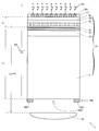
- FIGS. 1 to 19 An embodiment of a two-dimensional photonic crystal laser having a variable emission direction (hereinafter, simply referred to as a “two-dimensional photonic crystal laser”) according to the present invention will be described with reference to FIGS. 1 to 19.
- the terms “upper” and “lower” are used when explaining the relative positional relationship of each component of the two-dimensional photonic crystal laser, but these terms are two-dimensional photonic crystals. It does not limit the direction of the laser.
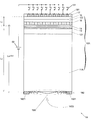
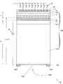
- the two-dimensional photonic crystal laser 1 of the first embodiment has a laminate 10 described later and a first electrode 181. It has a structure sandwiched between the second electrode 182 and the second electrode 182. Further, a lens 19 is provided on the side of the second electrode 182 opposite to the laminated body 10.
- the laminate 10 includes the substrate 11, the first clad layer 121, the active layer 13, the carrier block layer 14, the two-dimensional photonic crystal layer 15, and the second clad layer 122 in this order from the lower side of FIG. ,
- the contact layer 16 is laminated.
- the first electrode 181 is provided on the upper surface of the contact layer 16, and the second electrode 182 is provided on the lower surface of the substrate 11.
- the active layer 13 causes light emission in a specific emission wavelength band by injecting holes and electrons.
- a multiple-quantum well (MQW) in which a large number of thin films made of indium gallium arsenide (InGaAs) and thin films made of gallium arsenide (GaAs) are alternately laminated can be used.
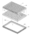
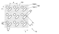
- a different refractive index region 152 having a refractive index different from that of the base material 151 is periodically formed in a plate-shaped base material 151 in a two-dimensional manner. It is arranged.
- the different refractive index region 152 typically has pores (refractive index ⁇ 1) formed in the base material 151. Instead of forming the pores, the different refractive index region 152 may be formed by embedding a member (different refractive index member) having a refractive index different from that of the base material 151 in the base material 151.
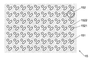
- a large number of different refractive index regions 152 are arranged in a square grid in the base material 151.
- one different refractive index region 152 is composed of a combination of two partial different refractive index regions, a first partial different refractive index region 1521 and a second partial different refractive index region 1522.
- the first partial refractive index region 1521 is elliptical, and the second partial refractive index region 1522 is circular.
- the long axis of the ellipse of the first partial refractive index region 1521 is arranged so as to face a direction inclined by 45 ° with respect to the line connecting the closest lattice points of the square lattice.
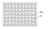
- each different refractive index region 152 may be composed of only one hole or a different refractive index member, or three. It may be composed of the above-mentioned pores or a member having a different refractive index. Further, the shape of the different refractive index region or each partial different refractive index region is not limited to the above example. For example, as shown in FIG. 4, the different refractive index region 152A composed of one pore having a plane shape of an equilateral triangle can be periodically arranged two-dimensionally.
- the different refractive index region 152 including the first partial different refractive index region 1521 and the second partial different refractive index region 1522 shown in FIGS. 2 and 3 also has a non-circular planar shape as a whole, and is therefore affected by interference. The disappearance of light can be suppressed.
- the substrate 11 and the first clad layer 121 are made of an n-type semiconductor, and the carrier block layer 14, the base material 151 of the two-dimensional photonic crystal layer 15, the second clad layer 122, and the contact layer 16 are p.
- a type semiconductor is used.
- a diode in which the p-type semiconductor is arranged on the first electrode 181 side and the n-type semiconductor is arranged on the second electrode 182 side with the active layer 13 interposed therebetween is formed, and the first electrode 181 side is formed. Holes are injected into the active layer 13 and electrons are injected into the active layer 13 from the second electrode 182 side.
- n-type GaAs is used for the substrate 11
- n-type aluminum gallium arsenide (AlGaAs) is used for the first clad layer 121
- p-type is used for the carrier block layer 14 and the second clad layer 122.
- AlGaAs can be used
- p-type GaAs can be used for the contact layer 16.
- a p-type semiconductor is used for the substrate 11 and the first clad layer 121, and an n-type semiconductor is used for the carrier block layer 14, the base material 151, the second clad layer 122, and the contact layer 16. It is also possible to use one consisting of. However, since n-type semiconductors are cheaper than p-type semiconductors, n-type semiconductors are placed on the substrate 11 which needs to be thicker than other layers as in the above example in order to reduce the cost of materials. It is preferable to use it.
- the positions of the active layer 13 and the two-dimensional photonic crystal layer 15 may be opposite to those shown in FIG. However, since each layer is sequentially produced on the substrate 11 when the two-dimensional photonic crystal laser 1 is manufactured, the two-dimensional photonic having pores (different refractive index region) is as shown in FIG. It is preferable to provide the active layer 13 on the substrate 11 side (the side to be produced first) rather than the crystal layer 15 because the active layer 13 can be precisely produced without being affected by unevenness due to the presence of pores. ..
- each layer constituting the laminate 10 is such that each layer (carrier block layer 14, two-dimensional photonic crystal layer 15, second clad layer 122, contact layer 16) located on the first electrode 181 side of the active layer 13 is used. than the thickness L 1 of the combined found the thickness L 2 of the combined layers (substrate 11 and the first cladding layer 121) in the second electrode 182 side is set to be sufficiently larger than that of the active layer 13 Is desirable. The reason will be described later together with the description of the operation of the two-dimensional photonic crystal laser 1.
- the first electrode 181 is divided into a large number of partial electrodes 1811 made of a conductor.
- the partial electrodes 1811 are arranged so as to be arranged in a row in the example of FIG. 5A, and are arranged so as to be distributed in a two-dimensional manner in the example of FIG. 5B.
- the planar shape of the partial electrode 1811 is rectangular in the example of FIG. 5A and square in the example of FIG. 5B, but is not limited to these shapes.
- Each partial electrode 1811 is connected to one electrode of the DC power supply 92 (a positive electrode when the contact layer 16 is made of a p-type semiconductor) via a switch 91 provided for each partial electrode 1811.
- the switch 91 for example, a field effect transistor can be used.
- the wiring including the switch 91 and the DC power supply 92 are not components of the two-dimensional photonic crystal laser 1.
- the distance between the partial electrodes 1811 will be described later together with the description of the operation of the two-dimensional photonic crystal laser 1.
- partial electrodes 1811 are provided than those shown in FIGS. 5A and 5B.
- FIGS. 5A and 5B more partial electrodes 1811 are provided than those shown in FIGS. 5A and 5B.
- hundreds of partial electrodes 1811 may be provided side by side in the vertical direction and the horizontal direction of the same figure.
- a layer (reflecting portion) 17 is provided.
- the partial electrode 1811 also has a role of reflecting the laser beam.
- the purpose of the reflective layer 17 is to increase the luminous efficiency by reflecting the laser beam emitted from the two-dimensional photonic crystal layer 15 toward the first electrode 181 and emitting it from the window portion 1822 of the second electrode 182. It is supposed to be.
- the second electrode 182 has a frame-shaped portion 1821 made of a conductor and a window portion 1822 which is a space inside the frame-shaped portion 1821.
- the window portion 1822 is arranged so as to face the region surrounding the plurality of partial electrodes 1811 of the first electrode 181.
- the second electrode 182 is connected to the other electrode of the DC power supply 92 (the negative electrode when the substrate 11 is made of an n-type semiconductor).
- the lens 19 uses a plano-convex lens in which one surface is a convex surface and the other surface is a flat surface.
- a lens having both surfaces convex may be used.
- a concave lens may be used as the lens 19. It is desirable that the lens 19 is arranged so as to be separated from the two-dimensional photonic crystal layer 15 by a distance L LP that is 0.5 to 2 times the focal length f of the lens 19, and is equivalent to the focal length f of the lens 19. It is more desirable that they are arranged apart by a distance. As a result, it is possible to prevent the diameter of the laser beam that has passed through the lens 19 from expanding.
- a lens such as a liquid lens (electrowetting lens) or a liquid crystal lens (Liquid crystal lens) in which one or both of the surface curvature and the focal length are variable by electrical control or the like.
- a prism in the present application, the prism is also included in the lens
- a control unit that performs electrical control or the like for changing the curvature and / or focal length of the lens surface is used.
- one or a plurality of adjacent partial electrodes 1811 (these one or a plurality of adjacent portions) among the switches 91 provided for each partial electrode 1811.
- the electrode 1811 is referred to as a "partial electrode group 1811A", and the region in which the partial electrode group 1811A exists is referred to as a "current supply region 21". See FIG. 6A).
- the switches 91 of the four partial electrodes 1811 included in the partial electrode group 1811A are turned on, but the number is not limited to this.
- a current flows between one of these or a plurality of partial electrodes 1811 and the second electrode 182 constituting the partial electrode group 1811A, holes are generated from each partial electrode 1811, and electrons are generated from the second electrode 182. , Each of which is supplied into the laminated body 10.
- the current flows so as to spread slightly in the direction parallel to the active layer 13 from each partial electrode 1811 toward the second electrode 182. Therefore, when the distance between the adjacent partial electrodes 1811 is smaller than a certain threshold value, the partial current injection region 221 which is the region where the current is injected from each partial electrode 1811 into the active layer 13 is the adjacent partial electrode 1811. It overlaps with a part of the partial current injection region 221 of the current injected from. As a result, an integrated current injection region 22 is formed in the active layer 13 (FIG. 6A).
- the active layer 13 light having a predetermined wavelength range determined by the material of the active layer 13 is generated in the current injection region 22.
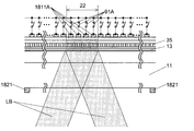
- the light having a wavelength corresponding to the period of the different refractive index region 152 in the two-dimensional photonic crystal layer 15 is a region (optical amplification region) of the two-dimensional photonic crystal layer 15 corresponding to the current injection region 22. Is amplified and laser oscillates. Then, the laser beam LB is emitted in a direction perpendicular to the two-dimensional photonic crystal layer 15, passes through the window portion 1822 of the second electrode 182, and enters the lens 19 (FIG. 7A).
- the laser beam LB is refracted in a direction corresponding to the approach position to the lens 19 and is emitted to the outside of the two-dimensional photonic crystal laser 1 in a direction inclined from a direction perpendicular to the two-dimensional photonic crystal layer 15.
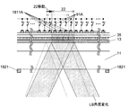
- the direction of the laser beam LB emitted to the outside of the two-dimensional photonic crystal laser 1 changes as follows by changing the partial electrode 1811 into which the current is injected.
- the switch 91 of the leftmost partial electrode 1811 in the figure is turned off, and the switch in FIG. 6A is shown.
- the switch 91 of the partial electrode 1811 on the right side where 91 was OFF is newly turned ON.
- the current supply region 21 moves to the right by one of the partial electrodes 1811, and the current injection region 22 and the optical amplification region in the active layer 13 also move to the right accordingly.
- the approach position of the laser beam LB emitted from the two-dimensional photonic crystal layer 15 to the lens 19 also moves to the right (FIG. 7B).
- the laser beam LB is refracted in a direction different from that in the case of FIG. 7A according to the difference in the approach position, and is emitted to the outside of the two-dimensional photonic crystal laser 1 in a different inclination direction.
- FIG. 8 shows how the laser beam LB moves in a one-dimensional shape, but if the partial electrodes 1811 are arranged in a two-dimensional shape as shown in FIG. 5B, the laser beam LB can be moved in a two-dimensional shape. ..
- the partial electrodes 1811 included in the partial electrode group 1811A are electrically switched and the surface of the lens is surfaced.
- the laser beam LB can also be scanned by varying the curvature and / or focal length.
- the response speed when electrically switching the partial electrodes 1811 included in the partial electrode group 1811A is faster than the response speed when changing the curvature of the lens surface or the focal length.
- the laser beam LB repeats the beam in one direction by electrically switching the partial electrodes 1811 included in the partial electrode group 1811A with respect to the partial electrodes 1811 arranged in a one-dimensional shape.
- Laser beam LB by scanning the laser beam LB in a direction different from the one direction (for example, a direction perpendicular to the one direction) by changing the curvature and / or focal distance of the surface of the lens while scanning. Can be scanned in two dimensions.
- each partial electrode 1811 Partial current injection regions 221 of the current injected from the current do not overlap each other, and a plurality of divided current injection regions 22 are formed in the active layer 13 (FIG. 9).
- the current injection region 22 divided in this way laser oscillation having low coherence (incoherent) occurs in the two-dimensional photonic crystal layer 15.
- FIGS. 6A and 6B by setting the distance between the adjacent partial electrodes 1811 so that the integrated current injection region 22 is formed, a highly coherent (coherent) laser beam is formed. Can be obtained.
- the distance between the partial electrodes 1811 can be appropriately determined by conducting a preliminary experiment or a simulation. As an example, the simulation was performed as follows under the conditions shown in FIG. 10A. In this simulation, when the distance (gap) between the partial electrodes 1811 is w p , the depth is sufficiently smaller than the distance from one partial electrode 1811 to the second electrode 182 (direction perpendicular to the active layer 13). Distance) d, with respect to the current density i 0 at the position B 0 intersecting the perpendicular h from the end of the partial electrode 1811, parallel to the active layer 13 from the position B 0 and opposite to the partial electrode 1811.
- I 1 / i 0 which is the ratio of the current densities i 1 at the position B 1 separated by the distance w, was obtained.
- the distance between the partial electrode 1811 and the second electrode 182 was (154 + d) ⁇ m
- d was calculated within the range of 3.5 to 12.5 ⁇ m
- w was calculated within the range of 0 to 65 ⁇ m.
- the width of the partial electrode 1811 was set to 30 ⁇ m, but the influence of this value on the calculation result is small.
- the calculation result is shown in FIG. 10B.
- the current density ratio i 1 / i 0 decreases as w increases, that is, as the distance from the end of the partial electrode 1811 increases.
- the distance w p between the partial electrodes 1811 is set to 2 w e or less.
- the partial current injection region 221 formed by the two partial electrodes 1811 expands in the direction parallel to the active layer 13 by a distance w e or more, so that the partial current injection regions 221 are connected to each other. Overlap. Therefore, an integral current injection region 22 can be formed, whereby a coherent laser beam can be obtained.
- each of the partial electrodes 1811 is preferable because the smaller the size, the finer the position of the current injection region 22 can be set, and thereby the inclination direction of the laser beam can be precisely controlled.
- the size of each partial electrode 1811 so that the current injection region 22 includes 10 to 50 partial electrodes 1811.
- the position of the current injection region 22 is moved by 2 to 10% of the area of the current injection region 22 by one ON / OFF operation of the switch 91.
- the partial electrodes 1811 are arranged two-dimensionally as shown in FIG. 5B, the partial electrodes 1811 are arranged so that 10 to 50 partial electrodes 1811 are arranged on one side of the rectangular current injection region 22.
- the size of each piece can be set.
- the size of the current injection region 22 and the number of switches 91 that influence it and are turned on at the same time are determined so that the required light output can be obtained according to the application of the two-dimensional photonic crystal laser 1.
- pulsed light requires an optical output of 1 W to several tens of W, and the size of the current injection region 22 is set to one side correspondingly. Is preferably within the range of a rectangle (including a square) of 10 ⁇ m to 500 ⁇ m.
- an optical output on the order of 100 W to 1000 W is required, and the size of the current injection region 22 is set within a rectangular range of 1 mm to 1 cm on each side. Is preferable.
- the light propagating in the two-dimensional photonic crystal layer is diffracted by a different refractive index region to increase the interference of light, thereby increasing the interference in the two-dimensional photonic crystal layer.
- the interference is too strong, the light is likely to be confined in the two-dimensional photonic crystal, so that the output of the light emitted to the outside of the two-dimensional photonic crystal may decrease. It has been known.
- the main different refractive index region corresponding to the first partial different refractive index region 1521 of the present embodiment
- the sub different refractive index region the same and the second partial different refractive index region
- a two-dimensional photonic crystal layer in which one different refractive index region consisting of two pores called the refractive index region 1522) or a member having a refractive index different from that of the base material is periodically arranged in a two-dimensional manner is used. ing.
- the diffracted light diffracted in the 180 ° direction by the main different refractive index region and the 180 ° direction by the sub-differential refractive index region are set so that the interference light with the diffracted diffracted light is strengthened or weakened according to the purpose.
- diffracted light (180 ° diffracted light) diffracted in the 180 ° direction by two partial different refractive index regions (first partial different refractive index region 1521 and second partial different refractive index region 1522) and 90.
- the two-dimensional photonic crystal layer is designed in consideration of the interference of diffracted light (90 ° diffracted light) diffracted in the ° direction. Specifically, as shown in FIG. 11, one of the two orthogonal directions in which the grid points of the square lattice are lined up closest to each other is the x direction, and the other is the y direction.
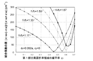
- ⁇ 180 and - ⁇ 90 are parameters that represent the intensity of diffracted light called the coupling coefficient, and can be either positive or negative.
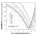
- d x was 0.262a for (b) and (c)
- f 1 / f 2 was 1.33 for (a) and (c)
- c 1 was changed in each calculation. As shown in FIG.
- It is desirable that
- the two-dimensional photonic crystal laser 1A shown in FIG. 13A is provided with a laminated body 10A instead of the laminated body 10 in the two-dimensional photonic crystal laser 1.
- the lens 19A is formed at a position facing the window portion 1822 on the surface of the second electrode 182 side. No lens is provided on the opposite side of the second electrode 182.
- the lens 19A is obtained by processing the surface of the substrate 11A into the shape of a Fresnel lens.
- a normal lens is divided into concentric regions, and the thickness of the region between the concentric circles is reduced to a predetermined value or less while maintaining the shape of the curved surface on one surface (the surface of the substrate 11A in this modification). By making it thinner, the surface is shaped like a saw blade.
- the configuration of the two-dimensional photonic crystal laser 1A other than the points described so far is the same as the configuration of the two-dimensional photonic crystal laser 1 described above.
- the two-dimensional photonic crystal laser 1B shown in FIG. 13B is provided with a laminated body 10B instead of the laminated body 10 in the two-dimensional photonic crystal laser 1.
- a lens 19B is formed at a position facing the window portion 1822 on the surface of the laminated body 10B on the second electrode 182 side. No lens is provided on the opposite side of the second electrode 182.
- the lens 19B processes the surface of the substrate 11B with an accuracy equal to or less than the wavelength of the laser beam, and appropriately forms a fine structure (metasurface) capable of controlling the phase of transmitted light in the plane. It is a lens called a metalens that has the function of a lens. The metal lens can be considered almost flat and can be thin enough.
- Other configurations of the two-dimensional photonic crystal laser 1B are the same as the configuration of the two-dimensional photonic crystal laser 1 described above.
- the size of the two-dimensional photonic crystal laser can be reduced as compared with the case where the lens 19 separate from the laminated body 10 is provided.
- a reflective layer (reflecting portion) 17 that reflects a laser beam is provided between the partial electrodes 1811 and at the end of the upper surface of the contact layer 16, but instead, the two-dimensional photonic A distributed Bragg reflector made of a conductive semiconductor material may be provided between the crystal layer 15 and the partial electrode 1811.
- the positional relationship between the distributed Bragg reflector and the second clad layer 122 and the contact layer 16 is not particularly limited.
- the laser beam emitted from the two-dimensional photonic crystal layer 15 toward the first electrode 181 can be reflected by the distributed Bragg reflector and emitted from the window portion 1822 of the second electrode 182 to increase the luminous efficiency.
- the distributed Bragg reflector can be constructed, for example, by a periodic structure in which layers made of doped GaAs and layers made of doped AlAs are alternately laminated.
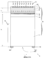
- the 2D photonic crystal laser 2 of the 2nd embodiment is the 2D photonic crystal laser of the 1st embodiment as shown in FIG.
- the two-dimensional photonic crystal of the first embodiment is provided with a laminate 30 including a two-dimensional photonic crystal layer 35 having a configuration different from that of the two-dimensional photonic crystal layer 15 in 1 and does not have a lens 19. It differs from the configuration of the laser 1.
- the two-dimensional photonic crystal laser 2 of the second embodiment has the same configuration as the two-dimensional photonic crystal laser 1 of the first embodiment. Therefore, the description of the common structure will be omitted, and the structure of the two-dimensional photonic crystal layer 35 will be described below.
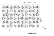
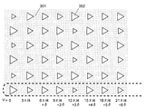
- the two-dimensional photonic crystal layer 35 has a different refractive index region 352 arranged in a plate-shaped base material 351 as follows.
- the planar shape of the different refractive index region 352 is composed of one equilateral triangle, but the shape of the different refractive index region 352 of the second embodiment is not limited to this example.
- the different refractive index region 352 actually provided in the two-dimensional photonic crystal layer 35 is shown by a solid line, and the square lattice, which is a basic two-dimensional lattice, is shown by a alternate long and short dash line, and the lattice points of the square lattice are shown.
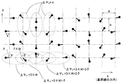
- FIG. 15B shows the positions of the square lattice (dashed line) and the center of gravity (black circle) of the actual different refractive index region 352.
- the x direction is defined as the direction of the reference line
- the design value of the inclination angle of the laser beam is defined as ⁇
- the azimuth angle ⁇ from the reference line is defined.
- the modulation phase that is, the angle formed by the deviation direction and the reference line (hereinafter referred to as “deviation azimuth angle”) ⁇ is (hereinafter referred to as “deviation azimuth angle”) ⁇ .
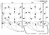
- the difference in deviation azimuth between the different refractive index regions 352 adjacent in the x direction ⁇ is (3/4) ⁇ (with respect to the explanation so far in this paragraph). See Patent Document 2 or 3).
- the shift azimuth ⁇ is set so that the values of the tilt angle ⁇ are different.
- the deviation azimuth ⁇ at each position is increased so that the difference ⁇ x of the deviation azimuth ⁇ between the different refractive index regions 352 adjacent to each other in the x direction increases by ⁇ in the x direction.
- a plurality of partial electrodes 1811 are provided so as to be arranged in the x direction.
- the active layer 13 light having a predetermined wavelength range is generated in the current injection region 22, and among this light, light having a wavelength corresponding to the period of the different refractive index region 152 in the two-dimensional photonic crystal layer 15 is emitted.
- the laser oscillates after being amplified in the region (optical amplification region) corresponding to the current injection region 22 in the two-dimensional photonic crystal layer 35.
- the laser beam LB emits to the outside of the two-dimensional photonic crystal laser 2 in a direction inclined by an inclination angle corresponding to an angle ⁇ that defines a deviation azimuth angle ⁇ in the optical amplification region of the two-dimensional photonic crystal layer 35. (Fig. 16A).
- the angle ⁇ that defines the deviation azimuth angle ⁇ differs depending on the position in one optical amplification region, so that the inclination angle of the laser beam LB is different. It is approximately the average value of the angle ⁇ in the photoamplification region.
- the position of the current injection region 22 moves, and the region where the light is amplified in the two-dimensional photonic crystal layer 35 also moves accordingly.
- the range of the deviation azimuth ⁇ and the value of the angle ⁇ that determines the azimuth angle ⁇ in the optical amplification region changes, so that the inclination angle of the laser beam LB also changes (FIG. 16B).
- the inclination angle of the laser beam LB emitted to the outside of the two-dimensional photonic crystal laser 2 changes, so that the laser beam LB can be scanned.
- the laser beam LB is emitted to the outside of the two-dimensional photonic crystal laser 2, it passes through the window portion 1822 of the second electrode 182. Therefore, the laser beam LB can be emitted without being attenuated by the second electrode 182.
- a square grid is used as the basic two-dimensional grid, but other two-dimensional grids such as a rectangular grid and a triangular grid may be used as the basic two-dimensional grid.
- a rectangular lattice of lattice constants a 1 a 1
- the modulation phase ⁇ of each grid point is ...(Five) Will be.
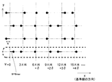
- the distance s between the lattice points and the actual center of gravity of the different refractive index region 352 is set to be the same at all the lattice points, and the direction of deviation (deviation azimuth) is modulated, as shown in FIG.
- is modulated between 0 and the maximum value s max.
- the modulation phase ⁇ can be set to a different value depending on the grid point by setting the angle ⁇ to a different value. As a result, the position of the current injection region into the active layer is moved, thereby moving the position of the optical amplification region, so that the angle of the emitted laser beam can be changed, whereby the laser beam can be scanned.
- the modulation phase ⁇ (x, y) obtained from the reciprocal lattice vector G'(x, y) ⁇ which depends on the position in the two-dimensional photonic crystal layer, is used, it is concrete.
- the modulation phase ⁇ (x, y) can be obtained as follows. For example, if the basic two-dimensional lattice is a square lattice of lattice constant a reciprocal lattice G '(x, y) components of the ⁇ g' x (x) and g 'y (y) is ...(Ten) It is represented by.
- the combination of positive and negative is arbitrary.
- the modulation phase ⁇ (x, y) can be calculated using Eq. (1). ... (11) Will be.
- ⁇ 'x (x), ⁇ ' y (y) respectively, ⁇ x (x), a first derivative of ⁇ y (y).
- ⁇ y (y) a first derivative of ⁇ y (y).
- a different inclination angle ⁇ (x, y) and / or an azimuth angle ⁇ (x, y) is set for each of the deviation azimuth setting areas 231, 232, 233, and the like.
- the same inclination angle ⁇ (x, y) and azimuth angle ⁇ (x, y) may be set in the same deviation azimuth setting area 231, 232, 233 ....
- a laser beam having y) and an azimuth angle ⁇ (x, y) can be obtained.
- the direction of the deviation of the position of the different refractive index region from the lattice point is modulated, but the same applies when the modulation is performed using other parameters such as the magnitude of the deviation and the area of the different refractive index region. Is.
- the reciprocal lattice vector G'(x, y) depends on the position in the 2D photonic crystal layer by the same calculation.
- the modulation phase ⁇ (x, y) can be obtained from ⁇ .
- a distributed Bragg reflector may be provided between the two-dimensional photonic crystal layer 15 and the partial electrode 1811 instead of the reflection layer 17. ..
- the present invention is not limited to the first embodiment, the second embodiment, and the modifications, and further modifications are possible.
Landscapes
- Physics & Mathematics (AREA)
- Condensed Matter Physics & Semiconductors (AREA)
- General Physics & Mathematics (AREA)
- Electromagnetism (AREA)
- Optics & Photonics (AREA)
- Semiconductor Lasers (AREA)
- Optical Modulation, Optical Deflection, Nonlinear Optics, Optical Demodulation, Optical Logic Elements (AREA)
Priority Applications (3)
| Application Number | Priority Date | Filing Date | Title |
|---|---|---|---|
| JP2022512568A JP7624742B2 (ja) | 2020-03-31 | 2021-03-30 | 2次元フォトニック結晶レーザ |
| EP21781520.8A EP4131675A4 (en) | 2020-03-31 | 2021-03-30 | PHOTONIC CRYSTAL LASER IN TWO DIMENSIONS |
| US17/916,116 US20230163566A1 (en) | 2020-03-31 | 2021-03-30 | Two-dimensional photonic-crystal laser |
Applications Claiming Priority (2)
| Application Number | Priority Date | Filing Date | Title |
|---|---|---|---|
| JP2020065047 | 2020-03-31 | ||
| JP2020-065047 | 2020-03-31 |
Publications (1)
| Publication Number | Publication Date |
|---|---|
| WO2021200994A1 true WO2021200994A1 (ja) | 2021-10-07 |
Family
ID=77928491
Family Applications (1)
| Application Number | Title | Priority Date | Filing Date |
|---|---|---|---|
| PCT/JP2021/013620 Ceased WO2021200994A1 (ja) | 2020-03-31 | 2021-03-30 | 2次元フォトニック結晶レーザ |
Country Status (4)
| Country | Link |
|---|---|
| US (1) | US20230163566A1 (cg-RX-API-DMAC7.html) |
| EP (1) | EP4131675A4 (cg-RX-API-DMAC7.html) |
| JP (1) | JP7624742B2 (cg-RX-API-DMAC7.html) |
| WO (1) | WO2021200994A1 (cg-RX-API-DMAC7.html) |
Families Citing this family (2)
| Publication number | Priority date | Publication date | Assignee | Title |
|---|---|---|---|---|
| CN120712700A (zh) * | 2023-02-21 | 2025-09-26 | 国立大学法人京都大学 | 二维光子晶体激光器 |
| JP2026010495A (ja) * | 2024-07-09 | 2026-01-22 | 住友電気工業株式会社 | フォトニック結晶面発光レーザおよびその製造方法 |
Citations (8)
| Publication number | Priority date | Publication date | Assignee | Title |
|---|---|---|---|---|
| US6026111A (en) * | 1997-10-28 | 2000-02-15 | Motorola, Inc. | Vertical cavity surface emitting laser device having an extended cavity |
| JP2001013306A (ja) * | 1999-06-28 | 2001-01-19 | Canon Inc | 可変焦点レンズ装置 |
| JP2005277219A (ja) | 2004-03-25 | 2005-10-06 | Kyoto Univ | フォトニック結晶レーザ |
| JP2008243962A (ja) | 2007-03-26 | 2008-10-09 | Kyoto Univ | 2次元フォトニック結晶面発光レーザ |
| JP2014082257A (ja) * | 2012-10-15 | 2014-05-08 | Kyoto Univ | 半導体レーザモジュール |
| WO2014136607A1 (ja) | 2013-03-08 | 2014-09-12 | 国立大学法人京都大学 | 2次元フォトニック結晶面発光レーザ |
| US20160248224A1 (en) | 2013-03-08 | 2016-08-25 | Japan Science And Technology Agency | Two-dimensional photonic crystal surface-emitting laser |
| JP2017123445A (ja) * | 2016-01-08 | 2017-07-13 | 浜松ホトニクス株式会社 | 分布帰還型半導体レーザ素子 |
Family Cites Families (13)
| Publication number | Priority date | Publication date | Assignee | Title |
|---|---|---|---|---|
| US5228049A (en) * | 1991-08-27 | 1993-07-13 | Xerox Corporation | Beam control in integrated diode laser and power amplifier |
| US7860141B2 (en) * | 2005-04-28 | 2010-12-28 | Kyoto University | Photonic crystal laser |
| US8379686B2 (en) * | 2005-09-02 | 2013-02-19 | Kyoto University | Two-dimensional photonic crystal surface-emitting laser light source |
| JP5070161B2 (ja) * | 2007-08-31 | 2012-11-07 | 独立行政法人科学技術振興機構 | フォトニック結晶レーザ |
| JP5627361B2 (ja) * | 2010-09-16 | 2014-11-19 | キヤノン株式会社 | 2次元フォトニック結晶面発光レーザ |
| JP6083703B2 (ja) * | 2012-02-28 | 2017-02-22 | 国立大学法人京都大学 | 2次元フォトニック結晶面発光レーザ |
| US10305248B2 (en) * | 2013-10-29 | 2019-05-28 | Hewlett Packard Enterprise Development Lp | High contrast grating optoelectronics |
| US10938177B2 (en) * | 2014-08-29 | 2021-03-02 | Kyoto University | Two-dimensional photonic crystal surface emitting laser |
| US10461501B2 (en) * | 2014-08-29 | 2019-10-29 | Kyoto University | Two-dimensional photonic crystal surface emitting laser |
| US9590389B2 (en) * | 2014-10-31 | 2017-03-07 | Nichia Corporation | Semiconductor laser element |
| WO2017150387A1 (ja) * | 2016-02-29 | 2017-09-08 | 国立大学法人京都大学 | 2次元フォトニック結晶面発光レーザ及びその製造方法 |
| JP7173478B2 (ja) * | 2017-12-22 | 2022-11-16 | 国立大学法人京都大学 | 面発光レーザ素子及び面発光レーザ素子の製造方法 |
| JP7279875B2 (ja) * | 2018-09-03 | 2023-05-23 | 国立大学法人京都大学 | 面発光レーザ素子及び面発光レーザ素子の製造方法 |
-
2021
- 2021-03-30 US US17/916,116 patent/US20230163566A1/en active Pending
- 2021-03-30 JP JP2022512568A patent/JP7624742B2/ja active Active
- 2021-03-30 EP EP21781520.8A patent/EP4131675A4/en active Pending
- 2021-03-30 WO PCT/JP2021/013620 patent/WO2021200994A1/ja not_active Ceased
Patent Citations (8)
| Publication number | Priority date | Publication date | Assignee | Title |
|---|---|---|---|---|
| US6026111A (en) * | 1997-10-28 | 2000-02-15 | Motorola, Inc. | Vertical cavity surface emitting laser device having an extended cavity |
| JP2001013306A (ja) * | 1999-06-28 | 2001-01-19 | Canon Inc | 可変焦点レンズ装置 |
| JP2005277219A (ja) | 2004-03-25 | 2005-10-06 | Kyoto Univ | フォトニック結晶レーザ |
| JP2008243962A (ja) | 2007-03-26 | 2008-10-09 | Kyoto Univ | 2次元フォトニック結晶面発光レーザ |
| JP2014082257A (ja) * | 2012-10-15 | 2014-05-08 | Kyoto Univ | 半導体レーザモジュール |
| WO2014136607A1 (ja) | 2013-03-08 | 2014-09-12 | 国立大学法人京都大学 | 2次元フォトニック結晶面発光レーザ |
| US20160248224A1 (en) | 2013-03-08 | 2016-08-25 | Japan Science And Technology Agency | Two-dimensional photonic crystal surface-emitting laser |
| JP2017123445A (ja) * | 2016-01-08 | 2017-07-13 | 浜松ホトニクス株式会社 | 分布帰還型半導体レーザ素子 |
Non-Patent Citations (1)
| Title |
|---|
| See also references of EP4131675A4 |
Also Published As
| Publication number | Publication date |
|---|---|
| EP4131675A4 (en) | 2023-09-20 |
| JP7624742B2 (ja) | 2025-01-31 |
| US20230163566A1 (en) | 2023-05-25 |
| JPWO2021200994A1 (cg-RX-API-DMAC7.html) | 2021-10-07 |
| EP4131675A1 (en) | 2023-02-08 |
Similar Documents
| Publication | Publication Date | Title |
|---|---|---|
| JP6080941B2 (ja) | 2次元フォトニック結晶面発光レーザ | |
| KR100759603B1 (ko) | 수직 공진기형 면발광 레이저 장치 | |
| US7664158B2 (en) | Two-dimensional photonic crystal surface-emitting laser | |
| CN111448725B (zh) | 发光装置及其制造方法 | |
| JP6083703B2 (ja) | 2次元フォトニック結晶面発光レーザ | |
| US20160248224A1 (en) | Two-dimensional photonic crystal surface-emitting laser | |
| TW202007031A (zh) | 發光裝置 | |
| TWI426673B (zh) | Two - dimensional photonic crystal surface emitting lasers | |
| JPWO2015008627A1 (ja) | 半導体レーザ装置 | |
| JP2003273456A (ja) | 2次元フォトニック結晶面発光レーザ | |
| JP4241905B2 (ja) | 2次元フォトニック結晶面発光レーザ | |
| JP2010245178A (ja) | 面発光レーザ | |
| JP7624742B2 (ja) | 2次元フォトニック結晶レーザ | |
| JP7103817B2 (ja) | 半導体発光素子 | |
| CN116073231B (zh) | 多波长拓扑腔面发射激光器阵列 | |
| JP5015641B2 (ja) | 2次元フォトニック結晶面発光レーザ | |
| JP6162465B2 (ja) | 半導体レーザ装置 | |
| WO2019077997A1 (ja) | 半導体発光素子 | |
| WO2021149618A1 (ja) | 光源モジュールおよび光変調モジュール | |
| JP5305423B2 (ja) | 2次元フォトニック結晶面発光レーザ光源 | |
| JPH07231138A (ja) | 面発光半導体レーザ | |
| JP2012533878A (ja) | マルチビームコヒーレントレーザ放射のダイオード光源 | |
| JP2686219B2 (ja) | 光子バンド構造のミラー | |
| JPS6257275A (ja) | 半導体レ−ザアレイ装置 | |
| US20250372944A1 (en) | Semiconductor laser element, and light source device using semiconductor laser element |
Legal Events
| Date | Code | Title | Description |
|---|---|---|---|
| 121 | Ep: the epo has been informed by wipo that ep was designated in this application |
Ref document number: 21781520 Country of ref document: EP Kind code of ref document: A1 |
|
| ENP | Entry into the national phase |
Ref document number: 2022512568 Country of ref document: JP Kind code of ref document: A |
|
| NENP | Non-entry into the national phase |
Ref country code: DE |
|
| ENP | Entry into the national phase |
Ref document number: 2021781520 Country of ref document: EP Effective date: 20221031 |