WO2021200518A1 - ストレッチャブル導電フィルム、センサ、電波吸収体およびリフレクタ - Google Patents
ストレッチャブル導電フィルム、センサ、電波吸収体およびリフレクタ Download PDFInfo
- Publication number
- WO2021200518A1 WO2021200518A1 PCT/JP2021/012436 JP2021012436W WO2021200518A1 WO 2021200518 A1 WO2021200518 A1 WO 2021200518A1 JP 2021012436 W JP2021012436 W JP 2021012436W WO 2021200518 A1 WO2021200518 A1 WO 2021200518A1
- Authority
- WO
- WIPO (PCT)
- Prior art keywords
- film
- conductive film
- base material
- metal film
- stretchable conductive
- Prior art date
- Legal status (The legal status is an assumption and is not a legal conclusion. Google has not performed a legal analysis and makes no representation as to the accuracy of the status listed.)
- Ceased
Links
Images


Classifications
-
- B—PERFORMING OPERATIONS; TRANSPORTING
- B32—LAYERED PRODUCTS
- B32B—LAYERED PRODUCTS, i.e. PRODUCTS BUILT-UP OF STRATA OF FLAT OR NON-FLAT, e.g. CELLULAR OR HONEYCOMB, FORM
- B32B15/00—Layered products comprising a layer of metal
- B32B15/04—Layered products comprising a layer of metal comprising metal as the main or only constituent of a layer, which is next to another layer of the same or of a different material
- B32B15/08—Layered products comprising a layer of metal comprising metal as the main or only constituent of a layer, which is next to another layer of the same or of a different material of synthetic resin
-
- H—ELECTRICITY
- H05—ELECTRIC TECHNIQUES NOT OTHERWISE PROVIDED FOR
- H05K—PRINTED CIRCUITS; CASINGS OR CONSTRUCTIONAL DETAILS OF ELECTRIC APPARATUS; MANUFACTURE OF ASSEMBLAGES OF ELECTRICAL COMPONENTS
- H05K9/00—Screening of apparatus or components against electric or magnetic fields
-
- H—ELECTRICITY
- H10—SEMICONDUCTOR DEVICES; ELECTRIC SOLID-STATE DEVICES NOT OTHERWISE PROVIDED FOR
- H10D—INORGANIC ELECTRIC SEMICONDUCTOR DEVICES
- H10D48/00—Individual devices not covered by groups H10D1/00 - H10D44/00
- H10D48/50—Devices controlled by mechanical forces, e.g. pressure
Definitions
- the present invention relates to a stretchable conductive film, a sensor using the film, a radio wave absorber, and a reflector.
- Patent Document 1 describes a tire pressure sensor in which a piezoelectric thin film is formed on a flexible film-like substrate.
- Patent Document 2 describes an electronic device capable of detecting strain and temperature, which comprises an electrode made of a metal nitride film on an insulating film base material such as polyimide.
- An object of the present invention is to provide a stretchable conductive film having excellent elasticity and flexibility in addition to conductivity.
- the present invention relates to the following stretchable conductive films and the like.
- a film-like base material and a metal film formed on at least one main surface of the base material are provided, and the base material has a stress of 10 N / mm 2 or less when strained by 10% at room temperature.
- ⁇ 3> The stretchable conductive film according to ⁇ 1> or ⁇ 2>, wherein the metal film has a thickness of 10 to 500 nm.
- the metal film is a film containing at least one selected from gold, silver, copper, iron, aluminum, nickel, manganese, cobalt, and an alloy containing at least one of these, ⁇ 1> to ⁇ 3>.
- the stretchable conductive film according to any one of. ⁇ 5> The stretchable conductive film according to any one of ⁇ 1> to ⁇ 4>, wherein the strain resistance increase rate A 20 represented by the following formula is 30% or less.
- a 20 100 ⁇ (R 20- R 0 ) / R 0 R 0 [ ⁇ ]: Electrical resistance when the stretchable conductive film is distorted by 0% at room temperature
- a sensor provided with the stretchable conductive film according to any one of ⁇ 5>.
- ⁇ 7> A radio wave absorber or reflector provided with the stretchable conductive film according to any one of ⁇ 1> to ⁇ 4>.
- a stretchable conductive film having excellent elasticity, flexibility, and conductivity is provided.
- FIG. 1 is a cross-sectional view showing an embodiment of the stretchable conductive film of the present invention.
- FIG. 2 is a diagram illustrating a method for measuring the strain resistance increase rate.
- the stretchable conductive film of the present invention includes a film-like base material and a metal film formed on at least one main surface of the base material.
- FIG. 1 is a cross-sectional view showing an embodiment of the stretchable conductive film 1.
- the metal film 20 may be formed on only one side of the base material 10, or may be formed on both sides, although not shown. Further, as shown in FIG. 1, the metal film 20 may be formed on the entire main surface of the base material 10, or may be formed at least partially, although not shown. Further, the metal film may be formed in the shape of various circuit patterns according to the use of the stretchable conductive film.
- the base material has a stress of 10 N / mm 2 or less when strained by 10% at room temperature.
- the stress is preferably 7 N / mm 2 or less, more preferably 5 N / mm 2 or less.
- the stress is preferably 0.1 N / mm 2 or more, more preferably 0.5 N / mm 2 or more, and further preferably 1 N / mm 2 or more.
- room temperature means 21 ° C to 25 ° C.
- the stress when strained by 10% is measured in accordance with JIS7161-1: 2014.
- the base material in the present invention is in the form of a film.
- the thickness of the base material is preferably 10 to 500 ⁇ m, more preferably 20 to 300 ⁇ m. When the thickness of the base material is 500 ⁇ m or less, the load does not become too large and the followability is good, and when it is 10 ⁇ m or more, the handleability is good.
- the base material is not particularly limited as long as it is a material that satisfies the above specific stress and has flexibility and elasticity, and examples thereof include elastomers and fibers. Elastomers are preferred from the standpoint of flexibility.
- elastomer for example, urethane rubber, silicone rubber, fluororubber, nitrile rubber, acrylic rubber, styrene rubber, chloroprene rubber, butyl rubber, ethylene rubber, propylene rubber, ethylene propylene rubber, natural rubber, and two or more of these are combined. Examples include a complex and the like.
- the stretchable conductive film of the present invention includes a metal film formed on at least one main surface of the base material.
- a ductile metal film is preferable because it easily follows the deformation of the base material.
- the ductile metal at least one selected from gold, silver, copper, iron, aluminum, nickel, manganese, cobalt and an alloy containing at least one of these is preferable.
- the oxygen atom concentration in the metal film is preferably 5.0 ⁇ 10 20 atom / cm 3 or less.
- the oxygen atom concentration in the metal film is more preferably 3.0 ⁇ 10 20 atom / cm 3 or less, and further preferably 1.0 ⁇ 10 20 atom / cm 3 or less.
- the lower limit is preferably 0 atom / cm 3 .
- the oxygen atom concentration in the metal film is measured at a depth (T 0.5 ) of 1/2 the thickness (T) of the metal film from the outermost surface of the metal film.
- the metal film can be formed by, for example, sputtering as described later.
- oxygen-containing substances are volatilized from water, oxygen, carbon dioxide, unreacted monomers and the like existing in the base material and the chamber, and are taken into the metal film. Therefore, in order to keep the oxygen atom concentration in the metal film within the above range, for example, the base material is heated before sputtering, and the inside of the chamber is degassed by degassing or the like, so that the water content and oxygen in the base material and the chamber are degassed.
- Carbon dioxide, unreacted monomer and the like can be mentioned.
- the thickness of the metal film is preferably 10 to 500 nm, more preferably 20 to 300 nm. It is preferable that the thickness of the metal film is within the range, because the stress difference with the base material is small and the followability is good. Further, the metal film may be a single-layer film or a multilayer film in which different metal layers are laminated. In the case of a multilayer film, it is preferable to satisfy the above thickness as a whole.
- the strain resistance increase rate A 20 represented by the following formula is preferably 30% or less, more preferably 20% or less.
- a 20 100 ⁇ (R 20- R 0 ) / R 0 R 0 [ ⁇ ]: Electrical resistance when the stretchable conductive film is distorted by 0% at room temperature
- strain resistance increase rate A 20 The smaller the strain resistance increase rate A 20 is, the more preferable it is because it means that the stretchable conductive film is excellent in elasticity and conductivity.
- the stretchable conductive film of the present invention can be produced by forming a metal film on at least one main surface of a film-like base material.
- a physical vapor deposition method such as a vacuum vapor deposition method, a sputtering method, an ion plating method, a chemical vapor deposition method (CVD) such as plasma CVD, optical CVD, laser CVD, electrolytic plating, chemical plating, etc.
- CVD chemical vapor deposition method
- a physical vapor deposition method is preferable, and a sputtering method is more preferable.
- the sputtering method is preferable from the viewpoint that the degree of vacuum is high, a large area can be formed, and the film thickness can be easily controlled.
- the target and the adherend are placed facing each other in the chamber of the vacuum device, and gas ions are accelerated by applying a voltage while supplying gas to irradiate the target material, and the target material is ejected from the target surface.
- the target material is laminated on the surface of the adherend.
- the target material contains a substance constituting a metal film.
- Examples of the sputtering method include a bipolar sputtering method, an ECR (electron cyclotron resonance) sputtering method, a magnetron sputtering method, and an ion beam sputtering method.
- the electrode used in the sputtering method may be a direct current (DC) power supply, an alternating current medium frequency (AC / MF) power supply, a high frequency (RF) power supply, or a high frequency power supply in which a direct current power supply is superimposed.
- DC direct current
- AC / MF alternating current medium frequency
- RF high frequency
- the temperature for heating the base material is preferably 50 to 200 ° C., preferably 80 to 180 ° C., more preferably 100 to 150 ° C., and the time for heating the base material is preferable. Is 1 to 100 minutes, more preferably 5 to 60 minutes, and more preferably 10 to 50 minutes. From the viewpoint of removing outgas, the pressure inside the chamber is preferably 1.0 ⁇ 10 -4 [Pa] or less, more preferably 5.0 ⁇ 10 -5 [Pa] or less.
- the stretchable conductive film of the present invention can be suitably used as various sensors such as a strain sensor, a temperature sensor, a heat flow sensor, and a magnetic sensor. Further, since the stretchable conductive film of the present invention is excellent in flexibility and elasticity, it can be applied to a portion accompanied by deformation. Therefore, it can be attached to curved surfaces such as pipes, electric wires, and living organisms with good followability, and the sensor sensitivity is stable. Therefore, for example, it is suitably used for various sensors installed inside tires, wearable sensors, etc., whose demand is expected to increase with the spread of automatic driving systems.
- the strain sensor of the present invention includes, for example, the stretchable conductive film of the present invention.
- the metal films themselves function as electrodes.
- the metal film is preferably an Al film.
- the strain sensor can measure the amount of strain by measuring the capacitance that changes with the deformation of the film.
- the temperature sensor of the present invention includes, for example, a Ni film as a metal film (conductive layer) of the stretchable conductive film of the present invention.
- the metal film itself functions as a sensor.
- the temperature sensor can measure the temperature by measuring the electrical resistance of the metal film that changes with the temperature change of the film.
- the heat flow sensor of the present invention includes, for example, an Fe-Pt alloy film as a metal film (conductive layer) of the stretchable conductive film of the present invention.
- the metal film itself functions as a sensor.
- the heat flow sensor can measure the heat flow by measuring the electromotive force of the metal film that changes with the temperature gradient of the film.
- the magnetic sensor of the present invention includes, for example, a magnetic thin film as a metal film (conductive layer) of the stretchable conductive film of the present invention.
- the magnetic thin film preferably contains at least one selected from the group consisting of Mn, Fe, Ni and Co.
- the metal film itself functions as a sensor.
- the magnetic sensor can measure the magnetic field strength by measuring the electrical signal that changes with the environmental magnetic field. Electrical signals include voltage, Hall voltage, current, resistance, and the like.
- the stretchable conductive film of the present invention has conductivity, it can be used as a member of a radio wave absorber or a reflector. Further, since the stretchable conductive film of the present invention is excellent in flexibility and elasticity, the radio wave absorber or reflector using the stretchable conductive film has high flexibility. Therefore, the workability is excellent, and roll molding becomes possible at the time of manufacturing.
- the radio wave absorber of the present invention is, for example, a ⁇ / 4 type radio wave absorber, in which a reflective layer, a dielectric layer, and an impedance matching layer are laminated in this order, and a stretcher of the present invention is applied to at least one of the reflective layer and the impedance matching layer.
- a bull conductive film can be used.
- the impedance matching layer may be applied to a support film such as polyethylene terephthalate by, for example, sputtering, vapor deposition, ion plating or coating (for example, bar coating). It can be produced by forming a non-porous film on one main surface of a base material by a film forming method.
- the material of the impedance matching layer may be a metal such as indium tin oxide (ITO), an alloy, an inorganic material such as a metal oxide, or an organic material such as a conductive polymer and carbon nanotubes. ..
- the impedance matching layer is preferably set to a sheet resistance in the range of 220 to 600 ⁇ / ⁇ .
- the dielectric layer in the radio wave absorber preferably has a relative permittivity of 2.0 to 20.0. With such a relative permittivity, the thickness of the dielectric layer can be easily adjusted, and the radio wave absorption performance of the radio wave absorber can be easily adjusted.
- the relative permittivity of the dielectric layer is, for example, the relative permittivity at 10 GHz measured according to the cavity resonance method.
- the dielectric layer is made of, for example, ethylene vinyl acetate copolymer, vinyl chloride resin, urethane resin, acrylic resin, acrylic urethane resin, polyethylene, polypropylene, silicone, polyethylene terephthalate, polyethylene naphthalate, polycarbonate, polyimide, and cycloolefin polymer. It is preferable to contain at least one polymer selected from the above group. Further, the dielectric layer may be formed as a single layer, or may be formed by a plurality of layers made of the same or different materials.
- the reflector of the present invention is used, for example, for controlling the reflection angle of a millimeter wave.
- a reflective layer, a dielectric layer, and a conductive pattern layer are laminated in this order, and the stretcher of the present invention is applied to at least one of the reflective layer and the conductive pattern layer.
- a bull conductive film can be used.
- the conductive pattern layer is formed on a support film such as polyethylene terephthalate by, for example, sputtering, vapor deposition, ion plating or coating (for example, bar coating). It can be produced by forming a non-porous film on one main surface of the base material by the method, and further forming a pattern on the non-porous film by laser processing, etching or the like.
- the material of the conductive pattern layer may be a metal such as indium tin oxide (ITO), an alloy, an inorganic material such as a metal oxide, or an organic material such as a conductive polymer and carbon nanotubes. ..
- the dielectric layer in the reflector preferably has a relative permittivity of 2.0 to 20.0. With such a relative permittivity, the thickness of the dielectric layer can be easily adjusted, and the radio wave absorption performance of the reflector can be easily adjusted.
- the relative permittivity of the dielectric layer is, for example, the relative permittivity at 10 GHz measured according to the cavity resonance method.
- the dielectric layer is made of, for example, ethylene vinyl acetate copolymer, vinyl chloride resin, urethane resin, acrylic resin, acrylic urethane resin, polyethylene, polypropylene, silicone, polyethylene terephthalate, polyethylene naphthalate, polycarbonate, polyimide, and cycloolefin polymer. It is preferable to contain at least one polymer selected from the above group. Further, the dielectric layer may be formed as a single layer, or may be formed by a plurality of layers made of the same or different materials.
- Example 1 ⁇ Manufacturing of stretchable conductive film (base material with metal film)>
- a base material a urethane rubber film (manufactured by Nihon Matai Co., Ltd., product number: Esmer PX98, thickness: 150 ⁇ m) having a stress of 2.9 N / mm 2 (elastic modulus 29 MPa) when strained by 10% at room temperature is used. board. After heat-treating the substrate at 140 ° C. for 30 minutes before film formation, the ultimate vacuum in the apparatus was increased to 1.5 ⁇ 10-5 [Pa]. Then, using a 3-inch Al target, DC sputtering was performed at an output of 200 W under an Ar atmosphere and a back pressure of 0.3 Pa to form a 100 nm metal film (Al layer) on the surface of the substrate.
- Example 2 As the base material, the same as in Example 1 except that a urethane rubber film (thickness: 30 ⁇ m) having a stress of 4.4 N / mm 2 (elastic modulus 44 MPa) when strained by 10% at room temperature was used. A metal film was formed on the surface of the substrate.
- Example 3 Except for using a urethane rubber film (manufactured by Kurabo Co., Ltd., product number: Cranzir, thickness: 50 ⁇ m) having a stress of 2.8 N / mm 2 (elastic modulus 28 MPa) when strained by 10% at room temperature as the base material. Made a metal film on the surface of the base material in the same manner as in Example 1.
- Example 4 A metal film was formed on the surface of the base material in the same manner as in Example 1 except that the ultimate vacuum degree in the apparatus was set to 5.0 ⁇ 10 -4 [Pa] without heat treatment of the base material.
- Example 5 A metal film was formed on the surface of the base material in the same manner as in Example 2 except that the ultimate vacuum degree in the apparatus was set to 5.0 ⁇ 10 -4 [Pa] without heat treatment of the base material.
- Example 6 A metal film was formed on the surface of the base material in the same manner as in Example 3 except that the ultimate vacuum degree in the apparatus was set to 5.0 ⁇ 10 -4 [Pa] without heat treatment of the base material.
- Example 7 A metal film was formed on the surface of the base material in the same manner as in Example 1 except that the Ni target was used instead of the Al target.
- Example 8 A metal film was formed on the surface of the base material in the same manner as in Example 1 except that the Cu target was used instead of the Al target.
- Example 1 A metal film was formed on the surface of the base material in the same manner as in Example 1 except that a polyethylene terephthalate film (thickness: 50 ⁇ m) having an elastic modulus of 3.0 GPa was used as the base material.
- the oxygen atom concentration in the metal film was measured by the following method. Using ADEPT-1010 manufactured by Albac Phi Co., Ltd., the concentration distribution of oxygen atoms in the metal film in the depth direction was investigated under the conditions of primary ion species Cs + and primary acceleration voltage of 3.0 kV. The depth was set to half the film thickness of the metal film, that is, a depth of 50 nm. The results are shown in Table 1 below.
- a x (%) 100 x (R x -R 0 ) / R 0 (Ro [ ⁇ ]: resistance value between terminals before stretching (at 0% strain), R x [ ⁇ ]: resistance value between terminals at X% strain)
- Table 1 below shows the resistance increase rates (A 20 , A 50 , A 100 ) when the strain is 20%, 50%, and 100%.
- the strain resistance increase rate (A 20 ) when the strain was 20% was evaluated based on the following criteria, and if it was 50% or less, it was passed. A: 30% or less B: 50% or less C: More than 50% D: Break
- the films of the examples are all excellent in flexibility, elasticity, and conductivity.
- the films of the examples are all excellent in flexibility, elasticity, and conductivity.
- the resistance increase due to strain is suppressed, and the flexibility, elasticity, and conductivity are further excellent. I understand.
- a reflective layer, a dielectric layer, and an impedance matching layer were laminated in this order, and a radio wave absorber using a base material with a metal film produced in Examples or Comparative Examples was produced as the reflective layer.
- Example 9 A dielectric layer having a relative permittivity of 2.6 composed of an acrylic resin layer having a thickness of 560 ⁇ m was laminated on the metal film side of the base material with a metal film produced in Example 3, and an impedance matching layer was further laminated. A ⁇ / 4 type radio wave absorber was created. The impedance matching layer was formed by forming an ITO layer on one side of a polyethylene terephthalate base material so that the sheet resistance was 377 ⁇ .
- the stretchable conductive film of the present invention can be used as a member of a radio wave absorber and is excellent in flexibility and elasticity, so that it can be installed on a curved surface.
- Example 10 A dielectric layer having a relative permittivity of 2.6 composed of an acrylic resin layer having a thickness of 500 ⁇ m was laminated on the metal film side of the base material with a metal film produced in Example 3, and a conductive pattern layer was further laminated. I created a reflector.
- the conductive pattern layer was prepared by patterning an Al film on one side of a polyethylene terephthalate base material.
- Example 3 A reflector was prepared in the same manner as in Example 10 except that the base material with a metal film prepared in Comparative Example 1 was used as the reflective layer.
- the stretchable conductive film of the present invention can be used as a member of a reflector, and also has excellent flexibility and elasticity, so that it can be installed on a curved surface.
- the stretchable conductive film of the present invention can be used as a member of various sensors such as a strain sensor, a temperature sensor, a heat flow sensor, and a magnetic sensor, and a radio wave absorber or a reflector. Further, since the stretchable conductive film of the present invention is excellent in flexibility and elasticity, it can be installed on a curved surface and can be applied to a place accompanied by deformation.
- Stretchable conductive film 10 ... Base material, 20 ... Metal film
Landscapes
- Engineering & Computer Science (AREA)
- Microelectronics & Electronic Packaging (AREA)
- Laminated Bodies (AREA)
Abstract
本発明は、フィルム状の基材と、前記基材の少なくとも一方の主面に形成された金属膜とを備え、前記基材は、室温で10%歪ませた際の応力が10N/mm2以下である、ストレッチャブル導電フィルムに関する。
Description
本発明は、ストレッチャブル導電フィルムおよび当該フィルムを用いたセンサ、電波吸収体およびリフレクタに関する。
近年、導電性を有するフィルム状の電子デバイスが開発され、その態様は多様化している。
たとえば特許文献1には、可撓性を有するフィルム状基板上に圧電体薄膜を形成したタイヤ空気圧センサが記載されている。
特許文献2には、ポリイミド等の絶縁性フィルム基材上に金属窒化膜からなる電極を備えた、歪および温度を検出可能な電子デバイスが記載されている。
たとえば特許文献1には、可撓性を有するフィルム状基板上に圧電体薄膜を形成したタイヤ空気圧センサが記載されている。
特許文献2には、ポリイミド等の絶縁性フィルム基材上に金属窒化膜からなる電極を備えた、歪および温度を検出可能な電子デバイスが記載されている。
しかしながら、従来のフィルム状電子デバイスは、伸縮性および柔軟性の点で開発の余地があった。
本発明は、導電性に加え、伸縮性および柔軟性に優れるストレッチャブル導電フィルムを提供することを目的とする。
本発明は、導電性に加え、伸縮性および柔軟性に優れるストレッチャブル導電フィルムを提供することを目的とする。
本発明は下記のストレッチャブル導電フィルム等に関する。
<1> フィルム状の基材と、前記基材の少なくとも一方の主面に形成された金属膜とを備え、前記基材は、室温で10%歪ませた際の応力が10N/mm2以下である、ストレッチャブル導電フィルム。
<2> 前記金属膜内の酸素原子濃度が5.0×10²⁰atom/cm3以下である、<1>に記載のストレッチャブル導電フィルム。
<3> 前記金属膜の厚さが10~500nmである<1>または<2>に記載のストレッチャブル導電フィルム。
<4> 前記金属膜が、金、銀、銅、鉄、アルミニウム、ニッケル、マンガン、コバルト及びこれらを少なくとも1種含む合金より選ばれる少なくとも1種を含む膜である、<1>~<3>のいずれか1に記載のストレッチャブル導電フィルム。
<5> 下記式に示される歪抵抗上昇率A20が30%以下である、<1>~<4>のいずれか1に記載のストレッチャブル導電フィルム。
A20=100×(R20-R0)/R0
R0[Ω]:ストレッチャブル導電フィルムを室温で0%歪ませた際の電気抵抗
R20[Ω]:ストレッチャブル導電フィルムを室温で20%歪ませた際の電気抵抗
<6> <1>~<5>のいずれか1に記載のストレッチャブル導電フィルムを備えたセンサ。
<7> <1>~<4>のいずれか1に記載のストレッチャブル導電フィルムを備えた電波吸収体またはリフレクタ。
<1> フィルム状の基材と、前記基材の少なくとも一方の主面に形成された金属膜とを備え、前記基材は、室温で10%歪ませた際の応力が10N/mm2以下である、ストレッチャブル導電フィルム。
<2> 前記金属膜内の酸素原子濃度が5.0×10²⁰atom/cm3以下である、<1>に記載のストレッチャブル導電フィルム。
<3> 前記金属膜の厚さが10~500nmである<1>または<2>に記載のストレッチャブル導電フィルム。
<4> 前記金属膜が、金、銀、銅、鉄、アルミニウム、ニッケル、マンガン、コバルト及びこれらを少なくとも1種含む合金より選ばれる少なくとも1種を含む膜である、<1>~<3>のいずれか1に記載のストレッチャブル導電フィルム。
<5> 下記式に示される歪抵抗上昇率A20が30%以下である、<1>~<4>のいずれか1に記載のストレッチャブル導電フィルム。
A20=100×(R20-R0)/R0
R0[Ω]:ストレッチャブル導電フィルムを室温で0%歪ませた際の電気抵抗
R20[Ω]:ストレッチャブル導電フィルムを室温で20%歪ませた際の電気抵抗
<6> <1>~<5>のいずれか1に記載のストレッチャブル導電フィルムを備えたセンサ。
<7> <1>~<4>のいずれか1に記載のストレッチャブル導電フィルムを備えた電波吸収体またはリフレクタ。
本発明によれば、伸縮性、柔軟性、導電性に優れるストレッチャブル導電フィルムが提供される。
本発明のストレッチャブル導電フィルムは、フィルム状の基材と、前記基材の少なくとも一方の主面に形成された金属膜とを備える。
図1はストレッチャブル導電フィルム1の一実施形態を示す断面図である。図1に示すように、金属膜20は基材10の片面のみに形成されていてもよく、図示しないが両面に形成されていてもよい。また、図1に示すように金属膜20は基材10の主面全面に形成されていてもよく、図示しないが少なくとも一部に形成されていてもよい。さらに、金属膜は、ストレッチャブル導電フィルムの用途に応じた種々の回路パターンの形状に形成されていてもよい。
<基材>
本発明において、基材は、室温で10%歪ませた際の応力が10N/mm2以下である。かかる応力が小さいほど基材が柔軟性・伸縮性を有することを意味する。上記応力は好ましくは7N/mm2以下、より好ましくは5N/mm2以下である。一方、基材が柔らかすぎると、基材の変形に対して金属膜の追従が追い付かなくなる。かかる観点から上記応力は好ましくは0.1N/mm2以上、より好ましくは0.5N/mm2以上、さらに好ましくは1N/mm2以上である。
ここで室温とは21℃~25℃を意味する。
また10%歪ませた際の応力とは、JIS7161-1:2014に準拠して測定される。
本発明において、基材は、室温で10%歪ませた際の応力が10N/mm2以下である。かかる応力が小さいほど基材が柔軟性・伸縮性を有することを意味する。上記応力は好ましくは7N/mm2以下、より好ましくは5N/mm2以下である。一方、基材が柔らかすぎると、基材の変形に対して金属膜の追従が追い付かなくなる。かかる観点から上記応力は好ましくは0.1N/mm2以上、より好ましくは0.5N/mm2以上、さらに好ましくは1N/mm2以上である。
ここで室温とは21℃~25℃を意味する。
また10%歪ませた際の応力とは、JIS7161-1:2014に準拠して測定される。
本発明における基材は、フィルム状である。基材の厚さは好ましくは10~500μm、より好ましくは20~300μmである。基材の厚さが500μm以下であれば、荷重が大きくなり過ぎず追従性が良好であり、10μm以上であれば、ハンドリング性が良好である。
基材は、上記特定の応力を満たし、柔軟性および伸縮性を有する材料であれば特に限定されず、エラストマー、繊維が挙げられる。柔軟性の観点からエラストマーが好ましい。
エラストマーとしては、例えば、ウレタンゴム、シリコーンゴム、フッ素ゴム、ニトリルゴム、アクリルゴム、スチレンゴム、クロロプレンゴム、ブチルゴム、エチレンゴム、プロピレンゴム、エチレンプロピレンゴム、天然ゴム、これらの2種以上を組み合わせた複合体等が挙げられる。
エラストマーとしては、例えば、ウレタンゴム、シリコーンゴム、フッ素ゴム、ニトリルゴム、アクリルゴム、スチレンゴム、クロロプレンゴム、ブチルゴム、エチレンゴム、プロピレンゴム、エチレンプロピレンゴム、天然ゴム、これらの2種以上を組み合わせた複合体等が挙げられる。
<金属膜>
本発明のストレッチャブル導電フィルムは、前記基材の少なくとも一方の主面に形成された金属膜を備える。
本発明のストレッチャブル導電フィルムは、前記基材の少なくとも一方の主面に形成された金属膜を備える。
金属膜としては基材の変形に追従しやすい点から延性金属の膜が好ましい。延性金属としては、金、銀、銅、鉄、アルミニウム、ニッケル、マンガン、コバルト及びこれらを少なくとも1種含む合金より選ばれる少なくとも1種が好ましい。
本発明のストレッチャブル導電フィルムにおいて、金属膜内の酸素原子濃度は好ましくは5.0×10²⁰atom/cm3以下である。金属膜内の酸素原子濃度はより好ましくは3.0×1020atom/cm3以下、さらに好ましくは1.0×1020atom/cm3以下である。また、不純物である酸素は金属膜内において少ないほど好ましいため、下限は0atom/cm3が好ましい。金属膜内の酸素原子濃度がかかる範囲であることで、伸縮性に優れた金属膜が得られる。これは金属膜内の酸素原子が少ないほど、金属膜の結晶性が上がり、延性に寄与する自由電子の数が増えることによると推測される。
なお金属膜内の酸素原子濃度は、金属膜の最表面から金属膜の厚さ(T)の1/2の深さ(T0.5)において測定される。
なお金属膜内の酸素原子濃度は、金属膜の最表面から金属膜の厚さ(T)の1/2の深さ(T0.5)において測定される。
金属膜は、後述するように例えばスパッタリングにより形成できる。この際に、基材中やチャンバー内に存在する水分、酸素、二酸化炭素、未反応モノマー等から酸素含有物が揮発することで金属膜内に取り込まれる。そこで金属膜内の酸素原子濃度を上記範囲とするには、例えば、スパッタリング前に、基材を加熱し、さらにチャンバー内を減圧等により脱ガスすることで、基材やチャンバー内の水分、酸素、二酸化炭素、未反応モノマー等を除去する方法が挙げられる。
金属膜の厚さは好ましくは10~500nm、より好ましくは20~300nmである。金属膜の厚さがかかる範囲であることで基材との応力差が小さくなり追従性が良好となるため好ましい。
また、金属膜は、単層膜であっても、異なる金属層を積層した多層膜であってもよい。
多層膜の場合は全体として上記厚さを満たすことが好ましい。
また、金属膜は、単層膜であっても、異なる金属層を積層した多層膜であってもよい。
多層膜の場合は全体として上記厚さを満たすことが好ましい。
上記構成を備える本発明のストレッチャブル導電フィルムは、下記式に示される歪抵抗上昇率A20が好ましくは30%以下、より好ましくは20%以下である。
A20=100×(R20-R0)/R0
R0[Ω]:ストレッチャブル導電フィルムを室温で0%歪ませた際の電気抵抗
R20[Ω]:ストレッチャブル導電フィルムを室温で20%歪ませた際の電気抵抗
A20=100×(R20-R0)/R0
R0[Ω]:ストレッチャブル導電フィルムを室温で0%歪ませた際の電気抵抗
R20[Ω]:ストレッチャブル導電フィルムを室温で20%歪ませた際の電気抵抗
歪抵抗上昇率A20が小さいほど、伸縮性と導電性に優れるストレッチャブル導電フィルムであることを意味し、好ましい。
<製造方法>
本発明のストレッチャブル導電フィルムは、フィルム状の基材の少なくとも一方の主面に金属膜を形成することで製造することができる。
本発明のストレッチャブル導電フィルムは、フィルム状の基材の少なくとも一方の主面に金属膜を形成することで製造することができる。
金属膜の形成には、例えば、真空蒸着法、スパッタリング法、イオンプレーティング法等の物理蒸着法、プラズマCVD、光CVD、レーザーCVD等の化学蒸着法(CVD)、電解めっき、化学めっき等のウェットプロセスが挙げられる。好ましくは、物理蒸着法、より好ましくは、スパッタリング法が挙げられる。なかでも、真空度が高く、大面積の形成が可能であり、膜厚を制御しやすい観点から、スパッタリング法が好ましい。
スパッタリング法では、真空装置のチャンバー内にターゲットおよび被着体を対向配置し、ガスを供給するとともに電圧を印加することによりガスイオンを加速しターゲット材料に照射させて、ターゲット表面からターゲット材料をはじき出して、ターゲット材料を被着体表面に積層させる。ここでターゲット材料は金属膜を構成する物質を含む。
スパッタリング法としては、例えば、2極スパッタリング法、ECR(電子サイクロトロン共鳴)スパッタリング法、マグネトロンスパッタリング法、イオンビームスパッタリング法などが挙げられる。
スパッタリング法に用いる電極は、直流(DC)電源、交流中周波(AC/MF)電源、高周波(RF)電源、直流電源を重畳した高周波電源の、いずれであってもよい。
スパッタリングにより金属膜を形成する際には、スパッタリング前に、基材を加熱し、さらにチャンバー内を減圧等により脱ガスすることが好ましい。これにより、基材中やチャンバー内に存在する水分、酸素、二酸化炭素、未反応モノマー等の酸素含有物が揮発し金属膜内に取り込まれることを防ぐことができる。
基材を加熱する温度は、基材の耐熱性の観点から、好ましくは50~200℃、好ましくは80~180℃、より好ましくは100~150℃であり、基材を加熱する時間は、好ましくは1~100分、より好ましくは5~60分、より好ましくは10~50分である。
チャンバー内は、アウトガス除去の観点から、好ましくは1.0×10⁻⁴[Pa]以下、より好ましくは5.0×10⁻⁵[Pa]以下に減圧することが好ましい。
チャンバー内は、アウトガス除去の観点から、好ましくは1.0×10⁻⁴[Pa]以下、より好ましくは5.0×10⁻⁵[Pa]以下に減圧することが好ましい。
<センサ>
本発明のストレッチャブル導電フィルムは、歪センサ、温度センサ、熱流センサ、磁気センサ等の各種センサとして好適に利用可能である。また、本発明のストレッチャブル導電フィルムは柔軟性、伸縮性に優れることから、変形を伴う箇所への適用が可能である。そのため配管、電線、生体等の曲面に追従性良く貼り付けられ、センサ感度が安定する。したがって、例えば、自動運転システムの普及に連れ需要が高まると考えられるタイヤ内部に設置される各種センサや、ウェアラブルセンサ等に好適に用いられる。
本発明のストレッチャブル導電フィルムは、歪センサ、温度センサ、熱流センサ、磁気センサ等の各種センサとして好適に利用可能である。また、本発明のストレッチャブル導電フィルムは柔軟性、伸縮性に優れることから、変形を伴う箇所への適用が可能である。そのため配管、電線、生体等の曲面に追従性良く貼り付けられ、センサ感度が安定する。したがって、例えば、自動運転システムの普及に連れ需要が高まると考えられるタイヤ内部に設置される各種センサや、ウェアラブルセンサ等に好適に用いられる。
本発明の歪センサは、例えば、本発明のストレッチャブル導電フィルムを備える。歪センサにおいて、金属膜は少なくとも1対設けられ、金属膜自体が電極として機能する。また歪センサにおいて、金属膜はAl膜であることが好ましい。歪センサでは、フィルムの変形に伴い変化する静電容量を計測することにより、歪量を測定できる。
本発明の温度センサは、例えば、本発明のストレッチャブル導電フィルムの金属膜(導電層)としてNi膜を備える。温度センサにおいて、金属膜自体がセンサとして機能する。温度センサでは、フィルムの温度変化に伴い変化する金属膜の電気抵抗を計測することにより、温度を測定できる。
本発明の熱流センサは、例えば、本発明のストレッチャブル導電フィルムの金属膜(導電層)としてFe-Pt合金膜を備える。熱流センサにおいて、金属膜自体がセンサとして機能する。熱流センサでは、フィルムの温度勾配に伴い変化する金属膜の起電力を計測することにより、熱流を測定できる。
本発明の磁気センサは、例えば、本発明のストレッチャブル導電フィルムの金属膜(導電層)として磁性薄膜を備える。磁性薄膜は、Mn、Fe、Ni、Coからなる群より選ばれる少なくとも1種を含むことが好ましい。磁気センサにおいて、金属膜自体がセンサとして機能する。磁気センサでは環境磁場に伴い変化する電気的シグナルを計測する事により、磁場強度を測定できる。電気的シグナルには電圧、ホール電圧、電流、抵抗等などが含まれる。
<電波吸収体、リフレクタ>
本発明のストレッチャブル導電フィルムは、導電性を有することから、電波吸収体またはリフレクタの部材として利用可能である。また、本発明のストレッチャブル導電フィルムは柔軟性、伸縮性に優れることから、これを用いた電波吸収体またはリフレクタは高い柔軟性を有する。そのため、施工性に優れ、また製造する際に、ロール成形が可能となる。
本発明のストレッチャブル導電フィルムは、導電性を有することから、電波吸収体またはリフレクタの部材として利用可能である。また、本発明のストレッチャブル導電フィルムは柔軟性、伸縮性に優れることから、これを用いた電波吸収体またはリフレクタは高い柔軟性を有する。そのため、施工性に優れ、また製造する際に、ロール成形が可能となる。
本発明の電波吸収体は、例えばλ/4型電波吸収体であり、反射層、誘電体層、インピーダンス整合層がこの順に積層され、反射層およびインピーダンス整合層の少なくとも一方に、本発明のストレッチャブル導電フィルムを用いることができる。
電波吸収体の反射層が、本発明のストレッチャブル導電フィルムである場合、インピーダンス整合層は、ポリエチレンテレフタレートなどの支持膜に、例えばスパッタリング、蒸着、イオンプレーティング又はコーティング(例えば、バーコーティング)等の成膜法によって基材の一方の主面上に無孔の膜を形成することによって作製できる。インピーダンス整合層の材料は、酸化インジウムスズ(ITO)等の金属、合金、及び金属酸化物等の無機材料であってもよいし、導電性高分子及びカーボンナノチューブ等の有機材料であってもよい。インピーダンス整合層は、シート抵抗が好ましくは220~600Ω/□の範囲に設定される。
電波吸収体における誘電体層は、好ましくは2.0~20.0の比誘電率を有する。かかる比誘電率であれば、誘電体層の厚みを調整しやすく、電波吸収体の電波吸収性能の調整が容易である。誘電体層の比誘電率は、例えば、空洞共振法に従って測定される10GHzにおける比誘電率である。誘電体層は、例えば、エチレン酢酸ビニル共重合体、塩化ビニル樹脂、ウレタン樹脂、アクリル樹脂、アクリルウレタン樹脂、ポリエチレン、ポリプロピレン、シリコーン、ポリエチレンテレフタレート、ポリエチレンナフタレート、ポリカーボネート、ポリイミド、及びシクロオレフィンポリマーからなる群より選ばれる少なくとも1つの高分子を含むことが好ましい。また、誘電体層は単一の層として形成されていてもよいし、同一又は異なる材料でできた複数の層によって形成されていてもよい。
本発明のリフレクタは、例えば、ミリ波の反射角度の制御に用いられ、反射層、誘電体層、導電パターン層がこの順に積層され、反射層および導電パターン層の少なくとも一方に、本発明のストレッチャブル導電フィルムを用いることができる。
リフレクタの反射層が、本発明のストレッチャブル導電フィルムである場合、導電パターン層は、ポリエチレンテレフタレートなどの支持膜に、例えばスパッタリング、蒸着、イオンプレーティング又はコーティング(例えば、バーコーティング)等の成膜法によって基材の一方の主面上に無孔の膜を形成し、さらに無孔の膜にレーザー加工及びエッチング等によってパターンを形成することによって作製できる。導電パターン層の材料は、酸化インジウムスズ(ITO)等の金属、合金、及び金属酸化物等の無機材料であってもよいし、導電性高分子及びカーボンナノチューブ等の有機材料であってもよい。
リフレクタにおける誘電体層は、好ましくは2.0~20.0の比誘電率を有する。かかる比誘電率であれば、誘電体層の厚みを調整しやすく、リフレクタの電波吸収性能の調整が容易である。誘電体層の比誘電率は、例えば、空洞共振法に従って測定される10GHzにおける比誘電率である。誘電体層は、例えば、エチレン酢酸ビニル共重合体、塩化ビニル樹脂、ウレタン樹脂、アクリル樹脂、アクリルウレタン樹脂、ポリエチレン、ポリプロピレン、シリコーン、ポリエチレンテレフタレート、ポリエチレンナフタレート、ポリカーボネート、ポリイミド、及びシクロオレフィンポリマーからなる群より選ばれる少なくとも1つの高分子を含むことが好ましい。また、誘電体層は単一の層として形成されていてもよいし、同一又は異なる材料でできた複数の層によって形成されていてもよい。
以下、実施例および比較例を用いて本発明をより具体的に説明する。
<ストレッチャブル導電フィルム(金属膜付き基材)の製造>
[実施例1]
基材として、室温で10%歪ませた際の応力が2.9N/mm2(弾性率29MPa)であるウレタンゴムフィルム(日本マタイ株式会社製、品番:エスマーPX98、厚さ:150μm)を用いた。製膜前に140℃で30分間の基材加熱処理を行った後、装置内の到達真空度を1.5×10-5[Pa]まで上げた。その後、3インチのAlターゲットを用いて、Ar雰囲気下、背圧0.3Pa条件下、出力200WでDCスパッタリングを行い、100nmの金属膜(Al層)を基材表面に製膜した。
[実施例1]
基材として、室温で10%歪ませた際の応力が2.9N/mm2(弾性率29MPa)であるウレタンゴムフィルム(日本マタイ株式会社製、品番:エスマーPX98、厚さ:150μm)を用いた。製膜前に140℃で30分間の基材加熱処理を行った後、装置内の到達真空度を1.5×10-5[Pa]まで上げた。その後、3インチのAlターゲットを用いて、Ar雰囲気下、背圧0.3Pa条件下、出力200WでDCスパッタリングを行い、100nmの金属膜(Al層)を基材表面に製膜した。
[実施例2]
基材として、室温で10%歪ませた際の応力が4.4N/mm2(弾性率44MPa)であるウレタンゴムフィルム(厚さ:30μm)を用いた以外は、実施例1と同様に、金属膜を基材表面に製膜した。
基材として、室温で10%歪ませた際の応力が4.4N/mm2(弾性率44MPa)であるウレタンゴムフィルム(厚さ:30μm)を用いた以外は、実施例1と同様に、金属膜を基材表面に製膜した。
[実施例3]
基材として、室温で10%歪ませた際の応力が2.8N/mm2(弾性率28MPa)であるウレタンゴムフィルム(クラボウ株式会社製、品番:クランジール、厚さ:50μm)を用いた以外は、実施例1と同様に、金属膜を基材表面に製膜した。
基材として、室温で10%歪ませた際の応力が2.8N/mm2(弾性率28MPa)であるウレタンゴムフィルム(クラボウ株式会社製、品番:クランジール、厚さ:50μm)を用いた以外は、実施例1と同様に、金属膜を基材表面に製膜した。
[実施例4]
基材加熱処理を行わず、装置内の到達真空度を5.0×10⁻⁴[Pa]としたこと以外は、実施例1と同様に、金属膜を基材表面に製膜した。
基材加熱処理を行わず、装置内の到達真空度を5.0×10⁻⁴[Pa]としたこと以外は、実施例1と同様に、金属膜を基材表面に製膜した。
[実施例5]
基材加熱処理を行わず、装置内の到達真空度を5.0×10⁻⁴[Pa]としたこと以外は、実施例2と同様に、金属膜を基材表面に製膜した。
基材加熱処理を行わず、装置内の到達真空度を5.0×10⁻⁴[Pa]としたこと以外は、実施例2と同様に、金属膜を基材表面に製膜した。
[実施例6]
基材加熱処理を行わず、装置内の到達真空度を5.0×10⁻⁴[Pa]としたこと以外は、実施例3と同様に、金属膜を基材表面に製膜した。
基材加熱処理を行わず、装置内の到達真空度を5.0×10⁻⁴[Pa]としたこと以外は、実施例3と同様に、金属膜を基材表面に製膜した。
[実施例7]
Alターゲットに替えてNiターゲットを用いたこと以外は、実施例1と同様に、金属膜を基材表面に製膜した。
Alターゲットに替えてNiターゲットを用いたこと以外は、実施例1と同様に、金属膜を基材表面に製膜した。
[実施例8]
Alターゲットに替えてCuターゲットを用いたこと以外は、実施例1と同様に、金属膜を基材表面に製膜した。
Alターゲットに替えてCuターゲットを用いたこと以外は、実施例1と同様に、金属膜を基材表面に製膜した。
[比較例1]
基材として、弾性率3.0GPaのポリエチレンテレフタレートフィルム(厚さ:50μm)を用いたこと以外は、実施例1と同様に、金属膜を基材表面に製膜した。
基材として、弾性率3.0GPaのポリエチレンテレフタレートフィルム(厚さ:50μm)を用いたこと以外は、実施例1と同様に、金属膜を基材表面に製膜した。
<金属膜内の酸素原子濃度測定>
上記実施例および比較例で作製した各金属膜付き基材について、以下の方法により金属膜内の酸素原子濃度を測定した。
アルバック・ファイ株式会社製ADEPT-1010を用い、一次イオン種Cs+、一次加速電圧3.0kV条件下で、金属膜中の酸素原子の深さ方向濃度分布を調べた。深さは、金属膜の膜厚の半分の深さ、すなわち50nmの深さとした。
結果を下記表1に示す。
上記実施例および比較例で作製した各金属膜付き基材について、以下の方法により金属膜内の酸素原子濃度を測定した。
アルバック・ファイ株式会社製ADEPT-1010を用い、一次イオン種Cs+、一次加速電圧3.0kV条件下で、金属膜中の酸素原子の深さ方向濃度分布を調べた。深さは、金属膜の膜厚の半分の深さ、すなわち50nmの深さとした。
結果を下記表1に示す。
<歪抵抗上昇率測定及び応力測定>
また、上記実施例および比較例で作製した各金属膜付き基材について、以下の方法により延伸実験を行い、歪に対する抵抗上昇率及び応力を測定した。
サンプルを巾10mm×長さ40mmに切り出し、図2に示すように卓上延伸機(リンカム社:顕微鏡用延伸ステージ)のチャック部にテスターを取り付け、室温、延伸速度50μm/sの条件下で歪に対して抵抗値及び応力を測定した。延伸前のチャック部間距離は15mmとした。
歪抵抗上昇率は以下の式で示される。
歪抵抗上昇率Ax(%)=100×(Rx-R0)/R0
(Ro[Ω]:延伸前(歪0%時)の端子間抵抗値、Rx[Ω]:歪X%時の端子間抵抗値)
また、上記実施例および比較例で作製した各金属膜付き基材について、以下の方法により延伸実験を行い、歪に対する抵抗上昇率及び応力を測定した。
サンプルを巾10mm×長さ40mmに切り出し、図2に示すように卓上延伸機(リンカム社:顕微鏡用延伸ステージ)のチャック部にテスターを取り付け、室温、延伸速度50μm/sの条件下で歪に対して抵抗値及び応力を測定した。延伸前のチャック部間距離は15mmとした。
歪抵抗上昇率は以下の式で示される。
歪抵抗上昇率Ax(%)=100×(Rx-R0)/R0
(Ro[Ω]:延伸前(歪0%時)の端子間抵抗値、Rx[Ω]:歪X%時の端子間抵抗値)
歪が20%、50%および100%の時の抵抗上昇率(A20、A50、A100)を下記表1に示す。
歪が20%の時の歪抵抗上昇率(A20)について下記基準に基づき評価し、50%以下であれば合格とした。
A:30%以下
B:50%以下
C:50%超
D:破断
歪が20%の時の歪抵抗上昇率(A20)について下記基準に基づき評価し、50%以下であれば合格とした。
A:30%以下
B:50%以下
C:50%超
D:破断

上記結果より、実施例のフィルムはいずれも柔軟性、伸縮性、導電性に優れていることが分かる。なかでも、金属膜内の酸素原子濃度を低減させた実施例1~3、7、8は、歪に伴う抵抗上昇が抑えられており、柔軟性、伸縮性、導電性にさらに優れていることが分かる。
<電波吸収体の製造>
反射層、誘電体層、インピーダンス整合層がこの順に積層され、反射層として、実施例または比較例で作製した金属膜付き基材を用いた電波吸収体を製造した。
反射層、誘電体層、インピーダンス整合層がこの順に積層され、反射層として、実施例または比較例で作製した金属膜付き基材を用いた電波吸収体を製造した。
[実施例9]
実施例3で作製した金属膜付き基材の金属膜側に、膜厚560μmのアクリル樹脂層からなる比誘電率2.6の誘電体層を積層し、さらに、インピーダンス整合層を積層して、λ/4型の電波吸収体を作成した。インピーダンス整合層は、ポリエチレンテレフタレート基材の片面に、シート抵抗が377ΩとなるようにITO層を成膜して作成した。
実施例3で作製した金属膜付き基材の金属膜側に、膜厚560μmのアクリル樹脂層からなる比誘電率2.6の誘電体層を積層し、さらに、インピーダンス整合層を積層して、λ/4型の電波吸収体を作成した。インピーダンス整合層は、ポリエチレンテレフタレート基材の片面に、シート抵抗が377ΩとなるようにITO層を成膜して作成した。
[比較例2]
反射層として、比較例1で作製した金属膜付き基材を用いたこと以外は実施例9と同様に、λ/4型の電波吸収体を作成した。
反射層として、比較例1で作製した金属膜付き基材を用いたこと以外は実施例9と同様に、λ/4型の電波吸収体を作成した。
<電波吸収体の屈曲試験>
上記実施例および比較例で得られた各電波吸収体の20mm×50mmの試験体を準備し、直径21.5mmのコルクポーラーに、インピーダンス整合層側が内側になるように試験体を巻き付けて屈曲させ、反射層におけるシワ発生有無を目視で確認した。
シワ無し:A
シワ発生:D
結果を下記表に示す。
上記実施例および比較例で得られた各電波吸収体の20mm×50mmの試験体を準備し、直径21.5mmのコルクポーラーに、インピーダンス整合層側が内側になるように試験体を巻き付けて屈曲させ、反射層におけるシワ発生有無を目視で確認した。
シワ無し:A
シワ発生:D
結果を下記表に示す。

上記結果より、本発明のストレッチャブル導電フィルムは、電波吸収体の部材として利用可能であり、また、柔軟性、伸縮性に優れることから、曲面にも設置できることが分かる。
<リフレクタの製造>
反射層、誘電体層、導電パターン層がこの順に積層され、反射層として、実施例または比較例で作製した金属膜付き基材を用いたリフレクタを製造した。
反射層、誘電体層、導電パターン層がこの順に積層され、反射層として、実施例または比較例で作製した金属膜付き基材を用いたリフレクタを製造した。
[実施例10]
実施例3で作製した金属膜付き基材の金属膜側に、膜厚500μmのアクリル樹脂層からなる比誘電率2.6の誘電体層を積層し、さらに、導電パターン層を積層して、リフレクタを作成した。導電パターン層は、ポリエチレンテレフタレート基材の片面に、Al膜をパターニングすることにより作成した。
実施例3で作製した金属膜付き基材の金属膜側に、膜厚500μmのアクリル樹脂層からなる比誘電率2.6の誘電体層を積層し、さらに、導電パターン層を積層して、リフレクタを作成した。導電パターン層は、ポリエチレンテレフタレート基材の片面に、Al膜をパターニングすることにより作成した。
[比較例3]
反射層として、比較例1で作製した金属膜付き基材を用いたこと以外は実施例10と同様に、リフレクタを作成した。
反射層として、比較例1で作製した金属膜付き基材を用いたこと以外は実施例10と同様に、リフレクタを作成した。
<リフレクタの屈曲試験>
上記実施例および比較例で得られた各リフレクタの20mm×50mmの試験体を準備し、直径21.5mmのコルクポーラーに、導電パターン層側が内側になるように試験体を巻き付けて屈曲させ、反射層におけるシワ発生有無を目視で確認した。
シワ無し:A
シワ発生:D
結果を下記表に示す。
上記実施例および比較例で得られた各リフレクタの20mm×50mmの試験体を準備し、直径21.5mmのコルクポーラーに、導電パターン層側が内側になるように試験体を巻き付けて屈曲させ、反射層におけるシワ発生有無を目視で確認した。
シワ無し:A
シワ発生:D
結果を下記表に示す。
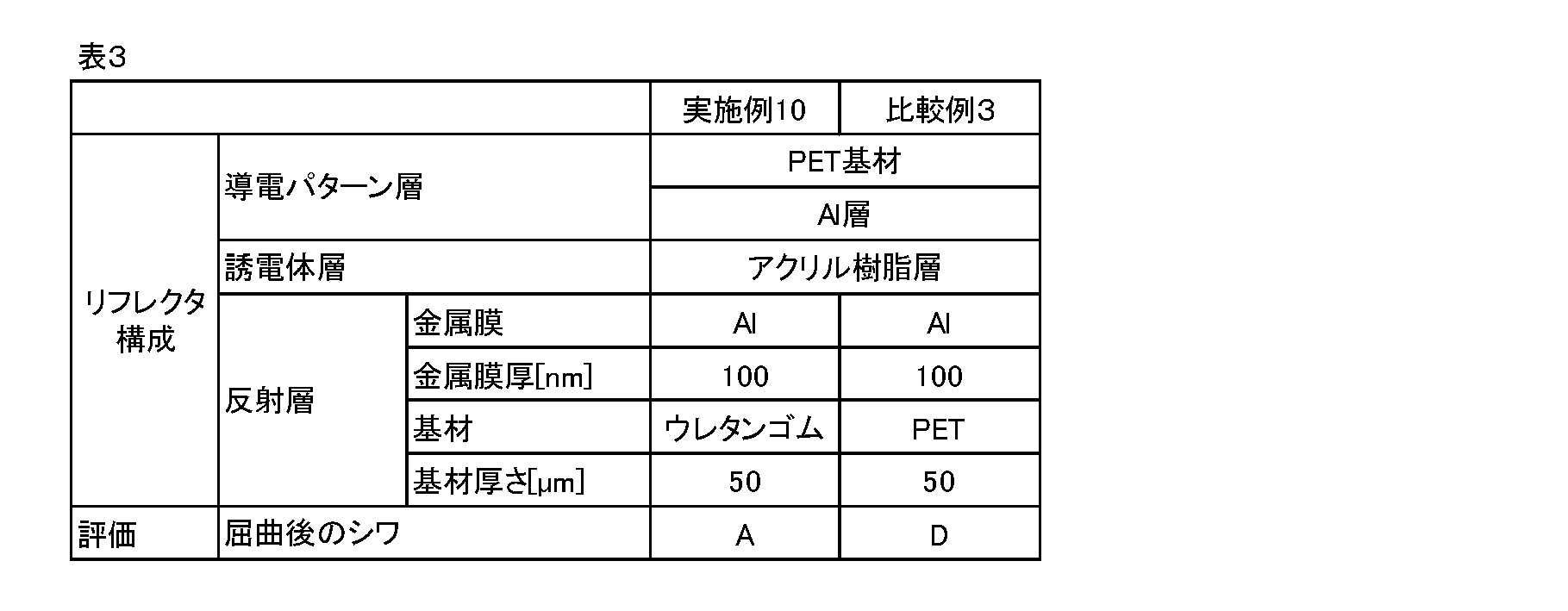
上記結果より、本発明のストレッチャブル導電フィルムは、リフレクタの部材として利用可能であり、また、柔軟性、伸縮性に優れることから、曲面にも設置できることが分かる。
本発明を詳細にまた特定の実施態様を参照して説明したが、本発明の精神と範囲を逸脱することなく様々な変更や修正を加えることができることは当業者にとって明らかである。本出願は2020年3月31日出願の日本特許出願(特願2020-064333)に基づくものであり、その内容はここに参照として取り込まれる。
本発明のストレッチャブル導電フィルムは、歪センサ、温度センサ、熱流センサ、磁気センサ等の各種センサや、電波吸収体またはリフレクタの部材として利用可能である。また、本発明のストレッチャブル導電フィルムは柔軟性、伸縮性に優れることから、曲面にも設置でき、変形を伴う箇所への適用が可能である。
1…ストレッチャブル導電フィルム、10…基材、20…金属膜
Claims (7)
- フィルム状の基材と、前記基材の少なくとも一方の主面に形成された金属膜とを備え、
前記基材は、室温で10%歪ませた際の応力が10N/mm2以下である、ストレッチャブル導電フィルム。 - 前記金属膜内の酸素原子濃度が5.0×10²⁰atom/cm3以下である、請求項1に記載のストレッチャブル導電フィルム。
- 前記金属膜の厚さが10~500nmである請求項1または2に記載のストレッチャブル導電フィルム。
- 前記金属膜が、金、銀、銅、鉄、アルミニウム、ニッケル、マンガン、コバルト及びこれらを少なくとも1種含む合金より選ばれる少なくとも1種を含む膜である、請求項1~3のいずれか1項に記載のストレッチャブル導電フィルム。
- 下記式に示される歪抵抗上昇率A20が30%以下である、請求項1~4のいずれか1項に記載のストレッチャブル導電フィルム。
A20=100×(R20-R0)/R0
R0[Ω]:ストレッチャブル導電フィルムを室温で0%歪ませた際の電気抵抗
R20[Ω]:ストレッチャブル導電フィルムを室温で20%歪ませた際の電気抵抗 - 請求項1~5のいずれか1項に記載のストレッチャブル導電フィルムを備えたセンサ。
- 請求項1~4のいずれか1項に記載のストレッチャブル導電フィルムを備えた電波吸収体またはリフレクタ。
Applications Claiming Priority (2)
| Application Number | Priority Date | Filing Date | Title |
|---|---|---|---|
| JP2020-064333 | 2020-03-31 | ||
| JP2020064333 | 2020-03-31 |
Publications (1)
| Publication Number | Publication Date |
|---|---|
| WO2021200518A1 true WO2021200518A1 (ja) | 2021-10-07 |
Family
ID=77929999
Family Applications (1)
| Application Number | Title | Priority Date | Filing Date |
|---|---|---|---|
| PCT/JP2021/012436 Ceased WO2021200518A1 (ja) | 2020-03-31 | 2021-03-24 | ストレッチャブル導電フィルム、センサ、電波吸収体およびリフレクタ |
Country Status (2)
| Country | Link |
|---|---|
| TW (1) | TW202145608A (ja) |
| WO (1) | WO2021200518A1 (ja) |
Cited By (1)
| Publication number | Priority date | Publication date | Assignee | Title |
|---|---|---|---|---|
| JP2023132076A (ja) * | 2022-03-10 | 2023-09-22 | 国立研究開発法人情報通信研究機構 | 電波吸収体 |
Citations (8)
| Publication number | Priority date | Publication date | Assignee | Title |
|---|---|---|---|---|
| JPH04131233A (ja) * | 1990-09-25 | 1992-05-01 | Bridgestone Corp | 可撓性部材のガスバリア性低下防止方法 |
| JPH10223003A (ja) * | 1997-02-12 | 1998-08-21 | Ichikoh Ind Ltd | 車両用灯具 |
| JP2001284880A (ja) * | 2000-03-31 | 2001-10-12 | Furuya Kinzoku:Kk | 電磁波遮蔽体 |
| JP2003042296A (ja) * | 2001-07-27 | 2003-02-13 | Suzutora:Kk | 帯電防止パッキン材 |
| JP2004095782A (ja) * | 2002-08-30 | 2004-03-25 | Emf:Kk | 電波吸収体及びその製造方法 |
| JP2015055615A (ja) * | 2013-09-13 | 2015-03-23 | 藤倉ゴム工業株式会社 | エラスティックフレキシブルセンサ |
| KR20170105987A (ko) * | 2016-03-11 | 2017-09-20 | (주)알킨스 | 신축성을 갖는 전기전도성 필름 및 그 제조방법 |
| WO2020067052A1 (ja) * | 2018-09-25 | 2020-04-02 | 積水化学工業株式会社 | 電波透過体 |
-
2021
- 2021-03-24 WO PCT/JP2021/012436 patent/WO2021200518A1/ja not_active Ceased
- 2021-03-30 TW TW110111546A patent/TW202145608A/zh unknown
Patent Citations (8)
| Publication number | Priority date | Publication date | Assignee | Title |
|---|---|---|---|---|
| JPH04131233A (ja) * | 1990-09-25 | 1992-05-01 | Bridgestone Corp | 可撓性部材のガスバリア性低下防止方法 |
| JPH10223003A (ja) * | 1997-02-12 | 1998-08-21 | Ichikoh Ind Ltd | 車両用灯具 |
| JP2001284880A (ja) * | 2000-03-31 | 2001-10-12 | Furuya Kinzoku:Kk | 電磁波遮蔽体 |
| JP2003042296A (ja) * | 2001-07-27 | 2003-02-13 | Suzutora:Kk | 帯電防止パッキン材 |
| JP2004095782A (ja) * | 2002-08-30 | 2004-03-25 | Emf:Kk | 電波吸収体及びその製造方法 |
| JP2015055615A (ja) * | 2013-09-13 | 2015-03-23 | 藤倉ゴム工業株式会社 | エラスティックフレキシブルセンサ |
| KR20170105987A (ko) * | 2016-03-11 | 2017-09-20 | (주)알킨스 | 신축성을 갖는 전기전도성 필름 및 그 제조방법 |
| WO2020067052A1 (ja) * | 2018-09-25 | 2020-04-02 | 積水化学工業株式会社 | 電波透過体 |
Cited By (1)
| Publication number | Priority date | Publication date | Assignee | Title |
|---|---|---|---|---|
| JP2023132076A (ja) * | 2022-03-10 | 2023-09-22 | 国立研究開発法人情報通信研究機構 | 電波吸収体 |
Also Published As
| Publication number | Publication date |
|---|---|
| TW202145608A (zh) | 2021-12-01 |
Similar Documents
| Publication | Publication Date | Title |
|---|---|---|
| US10959330B2 (en) | Metal-clad laminate, circuit board, and multilayer circuit board | |
| US11364714B2 (en) | Fluororesin base material, printed wiring board, and circuit module | |
| JP7176411B2 (ja) | フレキシブル電極及びセンサー素子 | |
| US4865711A (en) | Surface treatment of polymers | |
| JP6461532B2 (ja) | フッ素樹脂基材の製造方法及びプリント配線板の製造方法 | |
| WO2021200518A1 (ja) | ストレッチャブル導電フィルム、センサ、電波吸収体およびリフレクタ | |
| KR20130024890A (ko) | 성형체, 그 제조 방법, 전자 디바이스용 부재 및 전자 디바이스 | |
| KR20040026733A (ko) | 표면개질된 모재와의 접착력이 향상된 후막 형성 방법 및그의 장치 | |
| JP2015133256A (ja) | 透明導電積層体およびその製造方法ならびに静電容量方式タッチパネル | |
| WO1988008043A1 (en) | Surface treatment of polymers | |
| JP6262483B2 (ja) | 導電性フィルム基板およびその製造方法 | |
| JP6035679B2 (ja) | めっき積層体の製造方法、及びめっき積層体 | |
| KR102189938B1 (ko) | 신축성 전극, 이의 제조 방법 및 이를 포함하는 플렉시블 전자 소자 | |
| WO2022092204A1 (ja) | 積層フィルムおよび歪みセンサ | |
| JP3286467B2 (ja) | ポリイミドフイルム−金属薄膜の複合フイルムの製造方法 | |
| JP2008162245A (ja) | メッキ法2層銅ポリイミド積層フィルムおよびその製造方法 | |
| CN114245810A (zh) | 聚芳硫醚系树脂膜、金属层叠体、聚芳硫醚系树脂膜的制造方法、及金属层叠体的制造方法 | |
| KR20250084138A (ko) | 공중합체, 및 공중합체를 포함하는 수지 조성물 | |
| JP2007136800A (ja) | ガスバリア性積層フィルム、およびそれを用いた画像表示素子 | |
| JP2004193008A (ja) | 透明導電薄膜の成膜方法と透明導電薄膜、透明導電性フィルム及びタッチパネル | |
| WO2007013220A1 (ja) | 透明導電性フィルム、透明導電性シート、及びタッチパネル | |
| JP2022064501A (ja) | 金属層、導電性フィルム、および、金属層の製造方法 | |
| KR20170088322A (ko) | 표면 스트레인을 감소시키는 유연 기판 적층체 및 그를 포함하는 유연 전자 소자 | |
| KR20150107684A (ko) | 투명 도전성 기판의 제조방법 | |
| JP6806732B2 (ja) | 透明導電積層体の製造方法 |
Legal Events
| Date | Code | Title | Description |
|---|---|---|---|
| 121 | Ep: the epo has been informed by wipo that ep was designated in this application |
Ref document number: 21780667 Country of ref document: EP Kind code of ref document: A1 |
|
| NENP | Non-entry into the national phase |
Ref country code: DE |
|
| 122 | Ep: pct application non-entry in european phase |
Ref document number: 21780667 Country of ref document: EP Kind code of ref document: A1 |
|
| NENP | Non-entry into the national phase |
Ref country code: JP |