WO2021200415A1 - コンパレータ及びアナログ-デジタル変換器 - Google Patents
コンパレータ及びアナログ-デジタル変換器 Download PDFInfo
- Publication number
- WO2021200415A1 WO2021200415A1 PCT/JP2021/012086 JP2021012086W WO2021200415A1 WO 2021200415 A1 WO2021200415 A1 WO 2021200415A1 JP 2021012086 W JP2021012086 W JP 2021012086W WO 2021200415 A1 WO2021200415 A1 WO 2021200415A1
- Authority
- WO
- WIPO (PCT)
- Prior art keywords
- transistor
- signal
- comparator
- input
- differential
- Prior art date
- Legal status (The legal status is an assumption and is not a legal conclusion. Google has not performed a legal analysis and makes no representation as to the accuracy of the status listed.)
- Ceased
Links
Images




Classifications
-
- H—ELECTRICITY
- H03—ELECTRONIC CIRCUITRY
- H03M—CODING; DECODING; CODE CONVERSION IN GENERAL
- H03M1/00—Analogue/digital conversion; Digital/analogue conversion
- H03M1/12—Analogue/digital converters
- H03M1/34—Analogue value compared with reference values
- H03M1/38—Analogue value compared with reference values sequentially only, e.g. successive approximation type
- H03M1/46—Analogue value compared with reference values sequentially only, e.g. successive approximation type with digital/analogue converter for supplying reference values to converter
- H03M1/466—Analogue value compared with reference values sequentially only, e.g. successive approximation type with digital/analogue converter for supplying reference values to converter using switched capacitors
- H03M1/468—Analogue value compared with reference values sequentially only, e.g. successive approximation type with digital/analogue converter for supplying reference values to converter using switched capacitors in which the input S/H circuit is merged with the feedback DAC array
-
- H—ELECTRICITY
- H03—ELECTRONIC CIRCUITRY
- H03M—CODING; DECODING; CODE CONVERSION IN GENERAL
- H03M1/00—Analogue/digital conversion; Digital/analogue conversion
- H03M1/12—Analogue/digital converters
- H03M1/34—Analogue value compared with reference values
- H03M1/38—Analogue value compared with reference values sequentially only, e.g. successive approximation type
-
- H—ELECTRICITY
- H03—ELECTRONIC CIRCUITRY
- H03F—AMPLIFIERS
- H03F3/00—Amplifiers with only discharge tubes or only semiconductor devices as amplifying elements
- H03F3/45—Differential amplifiers
-
- H—ELECTRICITY
- H03—ELECTRONIC CIRCUITRY
- H03K—PULSE TECHNIQUE
- H03K5/00—Manipulating of pulses not covered by one of the other main groups of this subclass
- H03K5/01—Shaping pulses
- H03K5/08—Shaping pulses by limiting; by thresholding; by slicing, i.e. combined limiting and thresholding
-
- H—ELECTRICITY
- H03—ELECTRONIC CIRCUITRY
- H03M—CODING; DECODING; CODE CONVERSION IN GENERAL
- H03M1/00—Analogue/digital conversion; Digital/analogue conversion
- H03M1/06—Continuously compensating for, or preventing, undesired influence of physical parameters
- H03M1/0602—Continuously compensating for, or preventing, undesired influence of physical parameters of deviations from the desired transfer characteristic
- H03M1/0604—Continuously compensating for, or preventing, undesired influence of physical parameters of deviations from the desired transfer characteristic at one point, i.e. by adjusting a single reference value, e.g. bias or gain error
- H03M1/0607—Offset or drift compensation
-
- H—ELECTRICITY
- H03—ELECTRONIC CIRCUITRY
- H03M—CODING; DECODING; CODE CONVERSION IN GENERAL
- H03M1/00—Analogue/digital conversion; Digital/analogue conversion
- H03M1/06—Continuously compensating for, or preventing, undesired influence of physical parameters
- H03M1/0617—Continuously compensating for, or preventing, undesired influence of physical parameters characterised by the use of methods or means not specific to a particular type of detrimental influence
- H03M1/0626—Continuously compensating for, or preventing, undesired influence of physical parameters characterised by the use of methods or means not specific to a particular type of detrimental influence by filtering
-
- H—ELECTRICITY
- H03—ELECTRONIC CIRCUITRY
- H03M—CODING; DECODING; CODE CONVERSION IN GENERAL
- H03M1/00—Analogue/digital conversion; Digital/analogue conversion
- H03M1/06—Continuously compensating for, or preventing, undesired influence of physical parameters
- H03M1/08—Continuously compensating for, or preventing, undesired influence of physical parameters of noise
- H03M1/0854—Continuously compensating for, or preventing, undesired influence of physical parameters of noise of quantisation noise
-
- H—ELECTRICITY
- H03—ELECTRONIC CIRCUITRY
- H03M—CODING; DECODING; CODE CONVERSION IN GENERAL
- H03M1/00—Analogue/digital conversion; Digital/analogue conversion
- H03M1/12—Analogue/digital converters
- H03M1/124—Sampling or signal conditioning arrangements specially adapted for A/D converters
- H03M1/1245—Details of sampling arrangements or methods
-
- H—ELECTRICITY
- H03—ELECTRONIC CIRCUITRY
- H03M—CODING; DECODING; CODE CONVERSION IN GENERAL
- H03M1/00—Analogue/digital conversion; Digital/analogue conversion
- H03M1/66—Digital/analogue converters
- H03M1/662—Multiplexed conversion systems
Definitions
- the present disclosure relates to comparators and analog-to-digital converters.
- a double tail latch type comparator has been proposed (see Non-Patent Document 1).
- a transistor for switching on or off according to the logic of the clock signal is provided on the source side of a pair of transistors to which a differential input signal pair is input, and a latch circuit is provided on the drain side of the pair of transistors described above. Is connected, and another transistor for switching whether or not to perform the latch operation by the logic of the clock signal is provided on one end side of the latch circuit.
- ADC analog-to-digital converter
- the source side transistor of the pair of transistors in the comparator is turned off while sampling the differential input signal pair. Therefore, the potential of the source side path becomes indefinite, and the sampled differential input signal pair is affected by the parasitic capacitance of the input path, and the differential input node pair of the comparator is input voltage dependent. A certain error will occur. This error adversely affects the subsequent comparison operation of the comparator, and becomes a factor of lowering the accuracy of the ADC.
- the present disclosure provides a comparator and an analog-to-digital converter in which an error depending on the input voltage due to the input parasitic capacitance does not occur.
- two sources connected to each other, two gates to which a differential input signal pair is input, and a difference signal of the differential input signal pair are supported.
- a first transistor and a second transistor having two drains that output a differential output signal pair,
- a third transistor connected between the sources of the first transistor and the second transistor and the first reference voltage node and switched on or off according to the logic of the first signal.
- a fourth transistor connected between both sources of the first transistor and the second transistor and a second reference voltage node and switched on or off according to the logic of a second signal having a logic different from that of the first signal.
- a comparator is provided.
- the fourth transistor may be turned on during a period in which the first transistor and the second transistor are not performing the comparison operation of the difference signal of the differential input signal pair.
- the third transistor may be turned on intermittently within the period when the fourth transistor is off.
- a latch circuit for holding the differential output signal pair may be provided.
- a waveform shaping circuit for shaping the waveform of the differential output signal pair output from both drains of the first transistor and the second transistor is provided.
- a signal after waveform shaping by the waveform shaping circuit may be input to the latch circuit.
- the waveform shaping circuit may include two inverters that invert the logic of the differential output signal pair.
- a fifth transistor for switching whether or not to perform the holding operation by the latch circuit according to the logic of the first signal is provided.
- the fifth transistor may be turned on intermittently during the period when the fourth transistor is off.
- the fourth transistor may have a conductive type different from that of the third transistor.
- the first transistor, the second transistor, and the third transistor are N-type MOS transistors.
- the fourth transistor may be a P-type MOS transistor.
- the first transistor, the second transistor, and the third transistor are P-type MOS transistors.
- the fourth transistor may be an N-type MOS transistor.
- a pair of difference signals, a comparison circuit that outputs signals according to the difference, and With The comparison circuit A first comparator having sixth to ninth transistors having the same circuit configuration as the first to fourth transistors, and a first comparator.
- a comparator having a second comparator having tenth to thirteenth transistors having the same circuit configuration as the first to fourth transistors and a comparator may be provided.
- a first sampling switch that switches whether to sample one signal of a differential input signal pair and A first digital-to-analog converter that converts one of the sampled signals into a digital signal consisting of a plurality of bits in order bit by bit and outputs a signal with a voltage level corresponding to the unconverted bits.
- a second sampling switch that switches whether to sample the other signal of the differential input signal pair, and A second digital-to-analog converter that converts the other sampled signal into a digital signal consisting of a plurality of bits in order bit by bit and outputs a signal with a voltage level corresponding to the unconverted bits.
- a comparator that outputs a signal corresponding to the difference signal of the first differential input signal pair that pairs the output signal of the first digital-analog converter and the output signal of the second digital-analog converter.
- the comparator includes a control circuit for controlling the first digital-to-analog converter and the second digital-to-analog converter based on the output signal of the comparator.
- Two sources connected to each other, two gates to which the first differential input signal pair is input, and a differential output signal pair corresponding to the difference signal of the first differential input signal pair are output.
- a first transistor and a second transistor having one drain,
- a third transistor connected between the sources of the first transistor and the second transistor and the first reference voltage node and switched on or off according to the logic of the first signal.
- a fourth transistor connected between both sources of the first transistor and the second transistor and a second reference voltage node and switched on or off according to the logic of a second signal having a logic different from that of the first signal.
- an analog-to-digital converter having.
- a filter circuit for sampling and outputting the output signal of the first digital-analog converter and the output signal of the second digital-analog converter is provided.
- the comparator outputs a difference signal of a first differential input signal pair, which is a pair of an output signal of the first digital-analog converter and an output signal of the second digital-analog converter, and an output from the filter circuit. Outputs a signal corresponding to the difference signal of the second differential input signal pair.
- the comparator The first input terminal and the second input terminal to which the first differential input signal pair is input, and The third input terminal and the fourth input terminal to which the second differential input signal pair is input, and The difference signal of the first differential input signal pair input to the first input terminal and the second input terminal, and the second differential input signal input to the third input terminal and the fourth input terminal. It has a pair of difference signals and a comparison circuit that outputs signals according to the difference.
- the comparison circuit may include the first to fourth transistors.
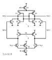
- the circuit diagram of the comparator according to the first embodiment A circuit diagram of a comparator according to a comparative example.
- the graph which shows the input voltage dependence of the input parasitic capacitance of the comparator of FIG. 1 and FIG.
- the circuit diagram of the sequential comparison type ADC4 provided with the comparator of FIG.
- the circuit diagram of the comparator according to the second embodiment The circuit diagram of the comparator according to the second embodiment.
- the circuit diagram of the comparator according to the third embodiment The circuit diagram of the comparator according to the 4th embodiment.
- the circuit diagram of the ADC provided with the filter circuit in addition to the capacitance DAC.
- the circuit diagram which shows an example of the internal structure of the comparator used in the ADC of FIG.
- FIG. 1 is a circuit diagram of the comparator 1 according to the first embodiment.
- the comparator 1 of FIG. 1 is used in, for example, a sequential comparison type ADC, but the application of the comparator 1 of FIG. 1 is not necessarily limited to the ADC.
- Differential input signal pairs Vin_p and Vin_n are input to the comparator 1 of FIG.
- the comparator 1 outputs a differential output signal pair Vout_p and Vout_n corresponding to the difference signal between the differential input signal pair Vin_p and Vin_n.
- the comparator 1 in FIG. 1 is a kind of double tail latch type comparator.
- Comparator 1 in FIG. 1 includes transistors (first to fourth transistors) Q1 to Q4.
- the sources of the transistor Q1 and the transistor Q2 are connected to each other, and the differential input signal pairs Vin_p and Vin_n are input to the gate, and the differential output signal pairs Vgm_p and Vgm_n are output from the drain.
- Transistor Q3 is connected between both sources of transistor Q1 and transistor Q2 and a first reference voltage node (for example, a ground node), and is switched on or off according to the logic of the first signal.
- the first signal is, for example, a clock signal Clk having a predetermined frequency.
- the clock signal Clk is at a high level
- the transistor Q43 is turned on, and the comparator 1 in FIG. 1 performs a comparison operation.
- the comparator 1 of FIG. 1 is in a stopped state without performing a comparison operation.
- the transistor Q4 is connected between both the sources of the transistor Q1 and the transistor Q2 and the second reference voltage node (for example, the power supply voltage node), and is turned on or off by the logic of the second signal having a logic different from that of the first signal.
- the second signal is, for example, the enable signal En.
- the enable signal En is turned on during the period when the comparator 1 of FIG. 1 is not performing the comparison operation.
- the transistor Q4 is turned on, the path connecting both sources of the transistor Q1 and the transistor Q2 (hereinafter, also referred to as a Tail node) is set to the power supply potential. That is, during the period when the comparator 1 of FIG.
- the Tail node connecting both sources of the transistor Q1 and the transistor Q2 is set to the power supply potential instead of floating.
- the voltage level of the Tail node connecting both sources of the transistor Q1 and the transistor Q2 is fixed to the power supply potential, and the input parasitic capacitance of the differential input node pair of the comparator 1 is fixed.
- the voltage dependence of Cin_p and Cin_n can be made sufficiently small.
- the transistors Q1 to Q3 in the comparator 1 of FIG. 1 are N-type MOS transistors, and the transistor Q4 is a P-type MOS transistor. As will be described later, it is also possible to reverse the conductive type of the transistors Q1 to Q4 from that in FIG.
- the comparator 1 of FIG. 1 includes a pull-up circuit 2 and a latch circuit 3 in addition to the transistors Q1 to Q4 described above.
- the pull-up circuit 2 has a transistor (fifth transistor) Q5 and a transistor (sixth transistor) Q6.
- the transistor Q5 and the transistor Q6 are, for example, P-type MOS transistors.
- a clock signal Clk is input to both the gates of the transistor Q5 and the transistor Q6.
- a power supply voltage node is connected to both sources of transistor Q5 and transistor Q6.
- Differential output signal pairs Vout_p and Vout_n are output from the drains of the transistor Q5 and the transistor Q6.
- the latch circuit 3 has transistors (7th to 13th transistors) Q7 to Q13.
- Transistors Q7 to Q10 are, for example, N-type MOS transistors, and transistors Q11 to Q13 are, for example, P-type MOS transistors.
- Differential output signal pairs Vgm_p and Vgm_n are input to the gates of the transistor Q7 and the transistor Q9.
- the first output node n1 is connected to each gate of the transistor Q10 and the transistor Q12 and each drain of the transistor Q7, the transistor Q8 and the transistor Q11, and Vout_p is output.
- a second output node n2 is connected to each gate of the transistor Q8 and the transistor Q11 and each drain of the transistor Q9, the transistor Q10 and the transistor Q12, and Vout_n is output.
- a power supply voltage node is connected to the source of the transistor Q13, and each source of the transistor Q11 and the transistor Q12 is connected to the drain of the transistor Q13.
- An inverted signal xClk of the clock signal Clk is input to the gate of the transistor Q13.
- Comparator 1 in FIG. 1 starts a comparison operation when the clock signal Clk transitions from the ground level (low level) to the power supply voltage level (high level). Before the comparator 1 of FIG. 1 starts the comparison operation, the clock signal Clk is low level, and the differential output signal pairs Vgm_p and Vgm_n are pulled up to the power supply level.
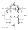
- FIG. 2 is a circuit diagram of the comparator 1a according to a comparative example.
- the same components as those in FIG. 1 are designated by the same reference numerals, and the differences will be mainly described below.
- the transistor Q4 of FIG. 1 is omitted.
- Other circuit configurations are the same as in FIG.
- the source potentials of the transistors Q1 and Q2 are in a floating state during the period when the comparison operation is not performed. Therefore, an input voltage-dependent error occurs in the voltage level of the differential input node pair due to the input parasitic capacitance of the differential input signal pair Vin_p and Vin_n input nodes of the comparator 1a.
- FIG. 3 is a graph showing the input voltage dependence of the input parasitic capacitances of the comparators 1 and 1a of FIGS. 1 and 2.
- FIG. 3 shows the simulation results.
- the horizontal axis of FIG. 3 is the input voltage [V]
- the vertical axis is the input parasitic capacitance [fF].
- the broken line waveform w1 in FIG. 3 shows the input voltage dependence of the comparator 1 in FIG. 1
- the solid line waveform w2 shows the input voltage dependence of the comparator 1a in FIG.
- the broken line waveform w1 in FIG. 3 is a result of simulating a state in which the enable signal En in the comparator 1 of FIG.
- the input parasitic capacitance fluctuates greatly according to the input voltage, but in the comparator 1 of FIG. 1, even if the input voltage changes, the fluctuation amount of the input parasitic capacitance is significantly suppressed. There is.
- FIG. 4 is a circuit diagram of a sequential comparison type ADC 4 provided with the comparator 1 of FIG.
- the sequential comparison type ADC4 of FIG. 4 shows an example of converting a differential input signal pair Vin_p and Vin_n into a 5-bit digital signal.
- the number of bits of the sequential comparison type ADC4 is arbitrary. Further, the circuit configuration of the sequential comparison type ADC4 is not limited to that shown in FIG.
- the sequential comparison type ADC 4 of FIG. 4 includes a first sampling switch 5, a second sampling switch 6, a first digital-analog converter (hereinafter, first DAC) 7, and a second digital-analog converter (second DAC). It includes 8, a comparator 1, and a control circuit (SAR logic) 10.
- first DAC7 and the second DAC8 are collectively referred to as a capacitance DAC20.
- the first sampling switch 5 switches whether or not to sample one of the differential input signal pair Vin_p and Vin_n signal Vin_p.
- the second sampling switch 6 switches whether or not to sample the other signal Vin_n of the differential input signal pair Vin_p and Vin_n.
- the first DAC7 converts one of the sampled signals Vin_p into a digital signal consisting of a plurality of bits in order bit by bit, and outputs a signal of a voltage level corresponding to the unconverted bits.
- the first DAC7 has five capacitors C1 to C5 having different capacities by a power of 2 and three switches (first to third switches) SW1 to SW3 connected to the capacitors C1 to C5.
- the first switch SW1 switches whether or not one end of the corresponding capacitors C1 to C5 is set to 0V.
- the second switch SW2 switches whether or not one end of the corresponding capacitors C1 to C5 is set to the common voltage Vcom.
- the third switch SW3 switches whether or not one end of the corresponding capacitors C1 to C5 is set to the reference voltage Vref.
- the common voltage Vcom is, for example, a voltage level of 1/2 of the reference voltage Vref.
- the first to third switches SW1 to SW3 are switched on or off based on the control signal from the control circuit 10.
- the control circuit 10 turns on the second switch SW2 at the start of the comparison operation. After that, the control circuit 10 turns on the first switch SW1 when it wants to lower the output node voltage Vin_p of the first DAC7, and turns on the third switch SW3 when it wants to raise the output node voltage Vin_p of the first DAC7.
- the second DAC8 converts the other sampled signal into a digital signal composed of a plurality of bits in order bit by bit, and outputs a signal of a voltage level corresponding to the unconverted bits.
- the second DAC 8 is configured in the same manner as the first DAC 7, and switches the first to third switches SW1 to SW3 based on the control signal from the control circuit 10 in the same manner as the first DAC 7.
- Comparator 1 has the configuration shown in FIG.
- a differential input signal pair Vin_p and Vin_n which is a pair of the output signal of the first DAC 7 and the output signal of the second DAC 8, is input to the comparator 1.
- the comparator 1 outputs a signal corresponding to the difference signal between the differential input signal vs. Vin_p and Vin_n.
- the control circuit 10 performs switching control of the first to third switches SW1 to SW3 in the first DAC7 and the second DAC8 based on the output signal of the comparator 1.
- the control signal Clk_adc is input to the ADC4.
- the control signal Clk_adc is inverted by the inverter 9a to generate the enable signal En.
- This enable signal En is input to the gate of the transistor Q4 in the comparator 1 of FIG.
- the enable signal En becomes a low level, and the transistor Q4 pulls up the Tail node connecting the sources of the transistors Q1 and Q2.
- the inverting signal of the control signal Clk_adc by the inverter 9b is input to the AND gate 11.
- the comparator 1 performs a comparison operation.
- the differential output signal pairs Vout_p and Vout_n output from the comparator 1 are input to the control circuit 10 and also to the NOR gate 12.
- the output of the NOR gate 12 becomes low level.
- the output of the AND gate 13 becomes low level, and the clock signal Clk is fixed at low level. Therefore, the comparator 1 is reset.
- the AND gate 11 calculates the logical product of the signal obtained by inverting the control signal Clk_adc by the inverter 9b and the output signal of the NOR gate 12. The output of the AND gate 11 becomes high level when the control signal Clk_adc is low level and both the differential output signals of the comparator 1 Vout_p and Vout_n are low level.
- the AND gate 13 calculates the logical product of the output signal of the AND gate 11 and the signal obtained by inverting the flag signal comp_end of the control circuit 10 with the inverter 14.
- the output of the AND gate 13 becomes high level when the flag signal comp_end of the control circuit 10 is low level and the output of the AND gate 11 becomes high level.
- the control circuit 10 raises the flag signal comp_end to a high level when all control with the capacitance DAC 20 is completed.
- the first sampling switch 5 and the second sampling switch 6 are turned on, and the differential input signal pairs Vin_p and Vin_n are sampled in the capacitance DAC20.
- the logic of the control signal Clk_adc is high level, and the clock signal Clk input to the comparator 1 is low level.
- the control circuit 10 turns on any of the first to third switches SW1 to SW3 connected to the capacitor of the most significant bit of the capacitance DAC20, and turns on the output voltage of the capacitance DAC20 ( Vin_p-Vin_n) is controlled.
- the control circuit 10 switches on or off the first to third switches SW1 to SW3 connected to the capacitors C1 to C5 one bit at a time in order from the upper bit of the capacitance DAC 20.
- the output voltage (Vin_p-Vin_n) of the capacitance DA gradually approaches zero.
- the output of the NOR gate 12 is transitioned to a low level after each comparison operation is completed.
- the clock signal Clk which is the output of the AND gate 13 becomes low level
- the transistor Q3 in the comparator 1 is turned off.
- the comparator 1 is reset after each comparison operation is completed.
- the output voltage of the capacitance DAC20 gradually approaches zero. Since the capacitance DAC20 in FIG. 4 has 5 bits, charge / discharge control of the capacitors C1 to c5 in the capacitance DAC20 is performed five times. When the charge / discharge control is completed, the control circuit 10 outputs a flag signal comp_end, the Clk becomes Low, and the comparator 1 is in the reset state. After that, when the control signal Clk_adc transitions from Low to High, sampling of the differential input signal pair Vin_p and Vin_n is performed again.
- Input parasitic capacitances Cin_p and Cin_n exist in the differential input node pairs n1 and n2 of the comparator 1 in FIG.
- the Tail node connecting the sources of the transistors Q1 and Q2 is pulled up to the power supply voltage by the transistor Q4 within the period when the comparator 1 does not perform the comparison operation, so that the differential input nodes are paired with n1 and n2. Even if there is an input parasitic capacitance, the input voltage dependence of the parasitic capacitance can be suppressed.
- control amount when controlling the capacitance DAC20 is not affected by the input voltage-dependent error of the differential input node pairs n1 and n2, and deterioration of various characteristics such as distortion of the ADC4 can be suppressed.
- FIG. 5 is a waveform diagram of the control signal Clk_adc, the enable signal En, and the clock signal Clk of the comparator 1 of FIG. As shown, the logic of the control signal Clk_adc and the enable signal En are opposite.
- the clock signal Clk intermittently goes high level multiple times within the period when the enable signal En is high level.
- the comparator 1 performs a comparison operation.
- the capacitance DAC 20 has five capacitors C1 to C5
- the comparator 1 performs a comparison operation in five times, and the first to third switches SW1 to SW3 connected to one end of the capacitors in order from the upper capacitor. Turn on either to control the charge and discharge to the capacitor.
- FIG. 6 is a circuit diagram of a sequential comparison type ADC 4a according to a comparative example provided with the comparator 1a of FIG.
- the ADC 4a of FIG. 6 has a configuration in which the inverter 9b is omitted from the ADC 4 of FIG.
- the enable signal En is not input to the comparator 1a in the ADC 4a of FIG.
- the logic of the control signal Clk_adc during the sampling period of the differential input signal vs. Vin_p and Vin_n is high level, and the clock signal Clk input to the comparator 1a is low level. That is, during the sampling period, the Tail node connecting the sources of the transistors Q1 and Q2 in the comparator 1 of FIG. 2 is floating, and the potential is indefinite.
- the input parasitic capacitances Cin_p and Cin_n of the comparator 1 exist in the output signal paths n1 and n2 of the capacitance DAC20 in the ADC 4a of FIG.
- the input parasitic capacitances Cin_p and Cin_n have input voltage dependence. More specifically, when the first sampling switch 5 and the second sampling switch 6 are turned on to sample the differential input signal pairs Vin_p and Vin_n, the differential input signal pairs Vin_p and Vin_n also have the input parasitic capacitances Cin_p and Cin_n. Is sampled.
- the charge sampled by the input parasitic capacitances Cin_p and Cin_n is determined by the capacitance values of the input parasitic capacitances Cin_p and Cin_n.
- the electric charge also has an input voltage dependence. This charge dependence gives an input voltage-dependent error to the control amount when controlling the capacitance DAC 20, and also gives an input voltage-dependent error to the conversion result of the ADC 4a. As a result, various characteristics such as distortion of ADC4a may be deteriorated.
- the Tail node connecting the sources of the transistors Q1 and Q2 in the comparator 1 is pulled to the power supply voltage by the transistor Q4. Therefore, there is no possibility that the input parasitic capacitances Cin_p and Cin_n have an input voltage dependence, and the capacitance DAC20 can be controlled accurately.
- the comparator 1 compares the tail nodes connecting the sources of the transistors Q1 and Q2 that generate signals corresponding to the difference signals between the differential input signals vs. Vin_p and Vin_n. Since the power supply voltage level is pulled up before starting the above, the input parasitic capacitances Cin_p and Cin_n of the comparator 1 do not have the input voltage dependence, and the comparison operation by the comparator 1 can be performed accurately. Therefore, the AD conversion accuracy of the ADC 4 having the comparator 1 built-in can be improved.
- FIG. 7 is a circuit diagram of the comparator 1b according to the second embodiment.
- the comparator 1b of FIG. 7 includes transistors Q21 to Q24.
- the transistors Q21 to Q23 are P-type MOS transistors, and the transistors Q24 are N-type MOS transistors.
- the inverted signal xEn of the enable signal En of FIG. 1 is input to the gate of the transistor Q24.
- the inverted signal of the clock signal Clk of FIG. 1 is input to the gate of the transistor Q23.
- the comparator 1b of FIG. 7 includes a pull-down circuit 15 and a latch circuit 3a.
- the pull-down circuit 15 includes a transistor Q45 and a transistor Q46 connected between the drains of the first and transistor Q2 and the ground terminal.
- An inversion signal xClk of the clock signal Clk is input to each gate of the transistor Q45 and the transistor Q46.
- the transistor Q45 and the transistor Q46 are N-type MOS transistors.
- the latch circuit 3a has transistors Q27 to Q33.
- the transistors Q27 to Q30 are P-type MOS transistors
- the transistors Q31 to Q33 are N-type MOS transistors.
- the comparator 1b of FIG. 7 has the opposite conductive type of each transistor to the comparator 1 of FIG. 1, and the connection order of the transistors connected between the power supply voltage node and the ground node is opposite to each other, but the comparison operation is performed. It is the same.
- Vgm_p charging speed ⁇ Vgm_n charging speed
- Vgm_p charging speed> Vgm_n charging speed Low
- Transistor Q24 is provided at the Tail node that connects the sources of transistors Q1 and Q2 in the comparator 1b of FIG. 7.
- the transistor Q24 is controlled by the inverting signal xEn of the enable signal En. While the ADC 4 is sampling, the transistor Q24 is turned on and pulled down to the ground level. In this state, the input parasitic capacitances Cin_p and Cin_n of the comparator 1b can sufficiently reduce the voltage dependence. This makes it possible to prevent deterioration of various characteristics such as distortion of the ADC4.
- FIG. 8 is a circuit diagram of the comparator 1c according to the third embodiment.
- the comparator 1c of FIG. 8 has N-type MOS transistors Q1 to Q4, Q14 to Q15, and P-type MOS transistors Q16 to Q19.
- Transistors Q16 and Q17 form a pull-up circuit 2a.
- the pull-up circuit 2 is connected to the drains of the transistors Q1 and Q2, but in FIG. 8, the pull-up circuit 2a is connected to the first output node and the second output nodes Vout_p and Vout_n.
- the latch circuit 3b of FIG. 8 has transistors Q14, Q15, Q18, and Q19.
- the gates of the transistors Q14 and Q18 and the drains of the transistors Q15 and Q19 are connected to the first output node Vout_p.
- the gates of the transistors Q15 and Q19 and the drains of the transistors Q14 and Q18 are connected to the second output node Vout_n.
- the drains of the transistors Q3 and Q4 are connected to the Tail node connecting the sources of the transistors Q1 and Q2, and when the enable signal En is low level, the transistor Q4 is turned on and the tail is turned on. Pull up the node to the power supply voltage level.
- the input parasitic capacitances Cin_p and Cin_n of the comparator 1c can sufficiently reduce the voltage dependence, and deterioration of various characteristics such as distortion of the ADC 4 can be prevented.
- the differential signal output pairs output from the drains of the transistors Q1 and Q2 are waveform-shaped and then input to the latch circuit 3.
- FIG. 9 is a circuit diagram of the comparator 1d according to the fourth embodiment.
- the comparator 1d of FIG. 9 includes inverters 16 and 17 connected to the drains of transistors Q1 and Q2.
- the output signals of the inverters 16 and 17 are input to the latch circuit 3c.
- the latch circuit 3c includes N-type MOS transistors Q14 to Q17, Q34, and Q35, and P-type MOS transistors Q18, Q19.
- the latch circuit 3c of FIG. 9 has a configuration in which transistors Q34 and Q35 are added to the latch circuit 3b of FIG.
- the transistor Q34 is connected between the drains of the transistors Q14 and Q18.
- the transistor Q35 is connected between the drains of the transistors Q15 and Q19.
- the output signals of the inverters 16 and 17 are input to each gate of the transistors Q34 and Q35.
- the inverters 16 and 17 perform waveform shaping to make the waveforms of the differential output signals vs. Vout_p and Vout_n output from the drains of the transistors Q1 and Q2 steep. By inputting the differential output signal pairs Vout_p and Vout_n to the latch circuit 3c via the inverters 16 and 17, the latch operation of the latch circuit 3c can be speeded up.
- the drains of the transistors Q3 and Q4 are connected to the Tail node connecting the sources of the transistors Q1 and Q2, and when the enable signal En is low level, the transistor Q4 is turned on and the tail is turned on. Pull up the node to the power supply voltage level.
- the input parasitic capacitances Cin_p and Cin_n of the comparator 1 can sufficiently reduce the voltage dependence, and deterioration of various characteristics such as distortion of the ADC 4 can be prevented.
- the comparators 1 to 1d of FIGS. 1 and 7 to 9 described above can be used in the ADC 4 of FIG. 4, but can also be applied to other types of ADCs, and the comparators 1 to 1 to be adapted to the ADC configuration. It may be necessary to partially change the internal configuration of 1d.
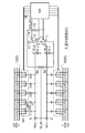
- FIG. 10 is a circuit diagram of an ADC 4b provided with a filter circuit 21 in addition to the capacitance DAC 20.
- the filter circuit 21 of FIG. 10 samples the differential output signal pairs Vin_p and Vin_n output from the capacitance DAC 20.
- the first differential output signal pairs Vin_p and Vin_n output from the capacitance DAC 20 and the second differential output signal pairs Vns_p and Vns_n output from the filter circuit 21 are input to the comparator 1e in the ADC 4b of FIG. NS. As described above, the comparator 1e of FIG.
- Vns_n Outputs a signal corresponding to the difference signal.
- the ADC 4b in FIG. 10 includes a filter circuit 21, the portion of the differential output signal of the capacitance DAC 20 that does not become zero is sampled by the filter circuit 21 and input to the comparator 1e. As a result, the accuracy of analog-to-digital conversion can be further improved.
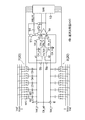
- FIG. 11 is a circuit diagram showing an example of the internal configuration of the comparator 1e used in the ADC 4b of FIG.
- the first input terminal TL1 and the second input terminal TL2 to which the first differential input signal pairs Vin_p and Vin_n are input and the third input terminal TL2 to which the second differential input signal pairs Vns_p and Vns_n are input. It includes an input terminal TL3, a fourth input terminal TL4, and a comparison circuit 22.
- the comparison circuit 22 is input to the first differential input signal pair Vin_p and Vin_n difference signals input to the first input terminal TL1 and the second input terminal TL2, and to the third input terminal TL3 and the fourth input terminal TL4.
- a signal corresponding to the difference signal between the second differential input signal vs. Vns_p and Vns_n is output.
- the comparison circuit 22 is a first differential input signal pair generated by connecting the first input terminal TL1 to the positive side and connecting the second input terminal TL2 to the negative side according to the difference signal between Vin_p and Vin_n.
- One differential output signal pair is output to the first output node n1 and the second output node n2.
- the voltage fluctuation amount of the third input terminal TL3 generated in response to the voltage fluctuation of the first output node n1 is equal to the voltage fluctuation amount of the fourth input terminal TL4 generated in response to the voltage fluctuation of the second output node n2.
- the comparison circuit 22 has a first comparator 24 and a second comparator 25.
- the first comparator 24 responds to the difference signal between the first differential input signal pair Vin_p and Vin_n generated by connecting the first input terminal TL1 to the positive side and the second input terminal TL2 to the negative side.
- the first differential output signal pair is output to the first output node n1 and the second output node n2.
- the second comparator 25 is a second comparator corresponding to a difference signal of a second differential input signal pair generated by connecting the third input terminal TL3 to the positive side and connecting the fourth input terminal TL4 to the negative side.
- the differential output signal pair is output from the first output node n1 and the first output node n2.
- the first comparator 24 has N-type MOS transistors Q41 and Q42.
- the first differential input signal Vin_p is input to the gate of the transistor Q41.
- the gate of transistor Q41 is on the positive side.
- the first differential input signal Vin_n is input to the gate of the transistor Q42.
- the gate of transistor Q42 is on the negative side.
- An N-type MOS transistor Q43 is connected between each source of the transistors Q41 and Q42 and the ground node.
- a clock signal Clk is input to the gate of the transistor Q43.
- the transistors Q41 and Q42 perform a comparison operation between the first differential input signal vs. Vin_p and Vin_n, and when the clock signal Clk is at a low level, the comparison operation is stopped.
- the drain of the transistor Q41 is connected to the first output node n1, and the drain of the transistor Q42 is connected to the second output node n2.
- a P-type MOS transistor Q68 is connected between the source of the transistors Q41 and Q42 and the power supply voltage node (second reference voltage node).
- An enable signal En is input to the gate of the transistor Q68.
- This transistor Q68 performs the same operation as the transistor Q4 of FIG.
- the second comparator 25 has N-type MOS transistors Q44 and Q45.
- the first differential input signal Vns_p is input to the gate of the transistor Q44.
- the gate of Transis Q44 is on the positive side.
- the second differential input signal Vns_n is input to the gate of the transistor Q45.
- the gate of transistor Q45 is on the negative side.
- An N-type MOS transistor Q46 is connected between the source of the transistors Q44 and Q45 and the ground node.
- a clock signal Clk is input to the gate of the transistor Q46.
- the transistors Q41 and Q42 perform a comparison operation between the first differential input signal vs. Vin_p and Vin_n, and when the clock signal Clk is at a low level, the comparison operation is stopped.
- the drains of the transistors Q44 and Q45 are connected to the first output node n1 and the second output node n2.
- a P-type MOS transistor Q69 is connected between the source of the transistors Q44 and Q45 and the power supply voltage node (second reference voltage node).
- An enable signal En is input to the gate of the transistor Q69. This transistor Q69 performs the same operation as the transistor Q4 of FIG.
- a pull-up circuit (first voltage setting circuit) 26 is connected to the first output node n1 and the second output node n2.
- the pull-up circuit 26 pulls up the first output node n1 and the second output node n2 to a high level when the clock signal Clk is at a low level, that is, within a period during which the comparison circuit 22 does not perform the comparison operation.
- the pull-up circuit 26 has a P-type MOS transistor Q47 connected to the first output node n1 and a P-type MOS transistor Q48 connected to the second output node n2.
- a clock signal Clk is input to the gates of the transistors Q47 and Q48.
- the latch circuit 30 includes P-type MOS transistors Q57 to Q60 and N-type MOS transistors Q61 to Q66.
- the first output node n1 is connected to each gate of the transistors Q57, Q61 and Q62.
- the second output node n2 is connected to each gate of the transistors Q58, Q64 and Q65.
- the gates of the transistors Q60 and Q66 and the drains of the transistors Q59 and Q63 are connected to the output terminal TL5 that outputs the differential output voltage Vout_p of the comparator 1e.
- the gates of the transistors Q59 and Q63 and the drains of the transistors Q65 and Q66 are connected to the output terminal TL6 that outputs the differential output voltage Vout_n of the comparator 1e.
- the comparator 1e in FIG. 11 pulls up the Tail node in each comparator within a period in which the comparator 1e does not perform the comparison operation, similarly to the comparators 1 to 1d according to the first to fourth embodiments described above.
- the input parasitic capacitances Cin_p and Cin_n of the comparator 1e can sufficiently reduce the voltage dependence and prevent deterioration of various characteristics such as distortion of the ADC 4b.
- the present technology can have the following configurations. (1) Two sources connected to each other, two gates to which a differential input signal pair is input, and two drains to output a differential output signal pair corresponding to a difference signal of the differential input signal pair.
- the first transistor and the second transistor having A third transistor connected between the sources of the first transistor and the second transistor and the first reference voltage node and switched on or off according to the logic of the first signal.
- a fourth transistor connected between both sources of the first transistor and the second transistor and a second reference voltage node and switched on or off according to the logic of a second signal having a logic different from that of the first signal. And, with a comparator.
- a fifth transistor for switching whether or not to perform the holding operation by the latch circuit according to the logic of the first signal is provided.
- the comparator according to any one of (4) to (6), wherein the fifth transistor is intermittently turned on within a period in which the fourth transistor is off.
- the first transistor, the second transistor, and the third transistor are N-type MOS transistors.
- the comparator according to any one of (1) to (8), wherein the fourth transistor is a P-type MOS transistor.
- the first transistor, the second transistor, and the third transistor are P-type MOS transistors.
- the comparator according to any one of (1) to (8), wherein the fourth transistor is an N-type MOS transistor.
- (11) The first input terminal and the second input terminal to which the first differential input signal pair is input, and The third input terminal and the fourth input terminal to which the second differential input signal pair is input, and The difference signal of the first differential input signal pair input to the first input terminal and the second input terminal, and the second differential input signal input to the third input terminal and the fourth input terminal.
- a pair of difference signals, a comparison circuit that outputs signals according to the difference, and With The comparison circuit A first comparator having sixth to ninth transistors having the same circuit configuration as the first to fourth transistors, and a first comparator.
- the comparator according to any one of (1) to (10), comprising a second comparator having tenth to thirteenth transistors having the same circuit configuration as the first to fourth transistors. (12) A first sampling switch that switches whether to sample one signal of the differential input signal pair, and A first digital-to-analog converter that converts one of the sampled signals into a digital signal consisting of a plurality of bits in order bit by bit and outputs a signal with a voltage level corresponding to the unconverted bits.
- a second sampling switch that switches whether to sample the other signal of the differential input signal pair
- a second digital-to-analog converter that converts the other sampled signal into a digital signal consisting of a plurality of bits in order bit by bit and outputs a signal with a voltage level corresponding to the unconverted bits.
- a comparator that outputs a signal corresponding to the difference signal of the first differential input signal pair that pairs the output signal of the first digital-analog converter and the output signal of the second digital-analog converter.
- the comparator includes a control circuit for controlling the first digital-to-analog converter and the second digital-to-analog converter based on the output signal of the comparator.
- a first transistor and a second transistor having one drain
- a third transistor connected between the sources of the first transistor and the second transistor and the first reference voltage node and switched on or off according to the logic of the first signal.
- a fourth transistor connected between both sources of the first transistor and the second transistor and a second reference voltage node and switched on or off according to the logic of a second signal having a logic different from that of the first signal. And, with an analog-to-digital converter.
- a filter circuit for sampling and outputting the output signal of the first digital-analog converter and the output signal of the second digital-analog converter is provided.
- the comparator outputs a difference signal of a first differential input signal pair, which is a pair of an output signal of the first digital-analog converter and an output signal of the second digital-analog converter, and an output from the filter circuit. Outputs a signal corresponding to the difference signal of the second differential input signal pair.
- the comparator The first input terminal and the second input terminal to which the first differential input signal pair is input, and The third input terminal and the fourth input terminal to which the second differential input signal pair is input, and The difference signal of the first differential input signal pair input to the first input terminal and the second input terminal, and the second differential input signal input to the third input terminal and the fourth input terminal. It has a pair of difference signals and a comparison circuit that outputs signals according to the difference.
Landscapes
- Engineering & Computer Science (AREA)
- Theoretical Computer Science (AREA)
- Power Engineering (AREA)
- Physics & Mathematics (AREA)
- Nonlinear Science (AREA)
- Analogue/Digital Conversion (AREA)
- Manipulation Of Pulses (AREA)
Priority Applications (2)
| Application Number | Priority Date | Filing Date | Title |
|---|---|---|---|
| US17/906,549 US12199631B2 (en) | 2020-03-30 | 2021-03-23 | Comparator and analog to digital converter |
| JP2022511995A JPWO2021200415A1 (https=) | 2020-03-30 | 2021-03-23 |
Applications Claiming Priority (2)
| Application Number | Priority Date | Filing Date | Title |
|---|---|---|---|
| JP2020-061390 | 2020-03-30 | ||
| JP2020061390 | 2020-03-30 |
Publications (1)
| Publication Number | Publication Date |
|---|---|
| WO2021200415A1 true WO2021200415A1 (ja) | 2021-10-07 |
Family
ID=77928666
Family Applications (1)
| Application Number | Title | Priority Date | Filing Date |
|---|---|---|---|
| PCT/JP2021/012086 Ceased WO2021200415A1 (ja) | 2020-03-30 | 2021-03-23 | コンパレータ及びアナログ-デジタル変換器 |
Country Status (3)
| Country | Link |
|---|---|
| US (1) | US12199631B2 (https=) |
| JP (1) | JPWO2021200415A1 (https=) |
| WO (1) | WO2021200415A1 (https=) |
Families Citing this family (2)
| Publication number | Priority date | Publication date | Assignee | Title |
|---|---|---|---|---|
| JP7729170B2 (ja) * | 2021-10-21 | 2025-08-26 | サンケン電気株式会社 | アナログデジタル変換器 |
| US12451901B2 (en) * | 2023-02-21 | 2025-10-21 | Microchip Technology Incorporated | Circuitry for converting a digital signal to an analog signal |
Citations (5)
| Publication number | Priority date | Publication date | Assignee | Title |
|---|---|---|---|---|
| US7250813B1 (en) * | 2005-10-21 | 2007-07-31 | National Semiconductor Corporation | Split amplifier architecture for cross talk cancellation |
| WO2012176250A1 (ja) * | 2011-06-23 | 2012-12-27 | パナソニック株式会社 | 差動スイッチ駆動回路及び電流ステアリング型デジタル・アナログ変換器 |
| JP2013187695A (ja) * | 2012-03-07 | 2013-09-19 | Sony Corp | コンパレータおよびad変換器 |
| JP2017163547A (ja) * | 2016-03-11 | 2017-09-14 | 株式会社ソシオネクスト | コンパレータで用いる回路 |
| WO2018216677A1 (ja) * | 2017-05-23 | 2018-11-29 | 株式会社村田製作所 | 比較回路 |
Family Cites Families (8)
| Publication number | Priority date | Publication date | Assignee | Title |
|---|---|---|---|---|
| JPS5938670B2 (ja) * | 1976-10-15 | 1984-09-18 | 日本電気株式会社 | 差信号増巾回路 |
| US4611130A (en) * | 1984-02-13 | 1986-09-09 | At&T Bell Laboratories | Floating input comparator with precharging of input parasitic capacitors |
| DE3736735A1 (de) * | 1986-11-12 | 1988-06-01 | Crystal Semiconductor Corp | Verfahren und schaltungsanordnung zum vermindern der erholzeit eines mos-differenz-spannungs-vergleichers |
| AU1094599A (en) * | 1997-10-17 | 1999-05-10 | Photobit Corporation | Low-voltage comparator with wide input voltage swing |
| US7088191B2 (en) * | 2004-09-29 | 2006-08-08 | Intel Corporation | Delay interpolation in a ring oscillator delay stage |
| US8471749B2 (en) * | 2011-07-18 | 2013-06-25 | Freescale Semiconductor, Inc. | Comparator |
| JP5942798B2 (ja) * | 2012-11-12 | 2016-06-29 | 富士通株式会社 | 比較回路およびa/d変換回路 |
| US9755655B1 (en) * | 2017-03-08 | 2017-09-05 | Xilinx, Inc. | Dynamic quantizers having multiple reset levels |
-
2021
- 2021-03-23 JP JP2022511995A patent/JPWO2021200415A1/ja active Pending
- 2021-03-23 US US17/906,549 patent/US12199631B2/en active Active
- 2021-03-23 WO PCT/JP2021/012086 patent/WO2021200415A1/ja not_active Ceased
Patent Citations (5)
| Publication number | Priority date | Publication date | Assignee | Title |
|---|---|---|---|---|
| US7250813B1 (en) * | 2005-10-21 | 2007-07-31 | National Semiconductor Corporation | Split amplifier architecture for cross talk cancellation |
| WO2012176250A1 (ja) * | 2011-06-23 | 2012-12-27 | パナソニック株式会社 | 差動スイッチ駆動回路及び電流ステアリング型デジタル・アナログ変換器 |
| JP2013187695A (ja) * | 2012-03-07 | 2013-09-19 | Sony Corp | コンパレータおよびad変換器 |
| JP2017163547A (ja) * | 2016-03-11 | 2017-09-14 | 株式会社ソシオネクスト | コンパレータで用いる回路 |
| WO2018216677A1 (ja) * | 2017-05-23 | 2018-11-29 | 株式会社村田製作所 | 比較回路 |
Also Published As
| Publication number | Publication date |
|---|---|
| JPWO2021200415A1 (https=) | 2021-10-07 |
| US12199631B2 (en) | 2025-01-14 |
| US20230163777A1 (en) | 2023-05-25 |
Similar Documents
| Publication | Publication Date | Title |
|---|---|---|
| US8421664B2 (en) | Analog-to-digital converter | |
| US8289198B2 (en) | Low power bit switches and method for high-voltage input SAR ADC | |
| CN1526202B (zh) | 具有单端输入的高速、高分辨率和低功耗的模/数转换器 | |
| US10447290B2 (en) | Reduced noise dynamic comparator for a successive approximation register analog-to-digital converter | |
| CN110235372B (zh) | 一种具有降低回扫噪声的双倍数据速率时间内插量化器 | |
| US8497795B2 (en) | Differential successive approximation analog to digital converter | |
| US10715167B2 (en) | Control circuit and control method of successive approximation register analog-to-digital converter | |
| US10148277B1 (en) | Current steering digital to analog converter with decoder free quad switching | |
| WO2021200415A1 (ja) | コンパレータ及びアナログ-デジタル変換器 | |
| JP4234543B2 (ja) | Ad変換器 | |
| JP7762141B2 (ja) | コンパレータ及びアナログ-デジタル変換器 | |
| KR101746064B1 (ko) | 축차 근사형 ad 변환기 | |
| CN114759911A (zh) | 一种低回踢噪声的可综合动态电压比较器 | |
| CN112994699B (zh) | 失调校准装置、逐次逼近型模数转换装置及失调校准方法 | |
| CN212435679U (zh) | 一种基于Vcm的超低功耗SAR ADC开关切换结构 | |
| JP3907633B2 (ja) | Nic回路及びadc回路 | |
| CN119401994A (zh) | 一种栅压自举开关电路 | |
| JP7622063B2 (ja) | コンパレータ及びアナログ-デジタル変換器 | |
| CN110048720B (zh) | 两步式快闪模/数转换器的参考电压控制电路 | |
| JP2019186841A (ja) | Ad変換器 | |
| WO2022085324A1 (ja) | 逐次比較型アナログ/デジタル変換器 | |
| WO2021106544A1 (ja) | コンパレータ回路およびadコンバータ | |
| WO2017081890A1 (ja) | 電圧変換回路、および、電子装置 | |
| CN104852741B (zh) | 非同步逐渐逼近式模拟至数字转换器 | |
| US20230155603A1 (en) | Ad converter |
Legal Events
| Date | Code | Title | Description |
|---|---|---|---|
| 121 | Ep: the epo has been informed by wipo that ep was designated in this application |
Ref document number: 21779258 Country of ref document: EP Kind code of ref document: A1 |
|
| ENP | Entry into the national phase |
Ref document number: 2022511995 Country of ref document: JP Kind code of ref document: A |
|
| NENP | Non-entry into the national phase |
Ref country code: DE |
|
| 122 | Ep: pct application non-entry in european phase |
Ref document number: 21779258 Country of ref document: EP Kind code of ref document: A1 |