WO2021200154A1 - 電子部品、リード部の接続構造及びリード部の接続方法 - Google Patents
電子部品、リード部の接続構造及びリード部の接続方法 Download PDFInfo
- Publication number
- WO2021200154A1 WO2021200154A1 PCT/JP2021/010810 JP2021010810W WO2021200154A1 WO 2021200154 A1 WO2021200154 A1 WO 2021200154A1 JP 2021010810 W JP2021010810 W JP 2021010810W WO 2021200154 A1 WO2021200154 A1 WO 2021200154A1
- Authority
- WO
- WIPO (PCT)
- Prior art keywords
- lead portion
- conductive wire
- lead
- wire
- connection structure
- Prior art date
- Legal status (The legal status is an assumption and is not a legal conclusion. Google has not performed a legal analysis and makes no representation as to the accuracy of the status listed.)
- Ceased
Links
Images


Classifications
-
- G—PHYSICS
- G01—MEASURING; TESTING
- G01K—MEASURING TEMPERATURE; MEASURING QUANTITY OF HEAT; THERMALLY-SENSITIVE ELEMENTS NOT OTHERWISE PROVIDED FOR
- G01K7/00—Measuring temperature based on the use of electric or magnetic elements directly sensitive to heat ; Power supply therefor, e.g. using thermoelectric elements
- G01K7/16—Measuring temperature based on the use of electric or magnetic elements directly sensitive to heat ; Power supply therefor, e.g. using thermoelectric elements using resistive elements
- G01K7/22—Measuring temperature based on the use of electric or magnetic elements directly sensitive to heat ; Power supply therefor, e.g. using thermoelectric elements using resistive elements the element being a non-linear resistance, e.g. thermistor
-
- B—PERFORMING OPERATIONS; TRANSPORTING
- B23—MACHINE TOOLS; METAL-WORKING NOT OTHERWISE PROVIDED FOR
- B23K—SOLDERING OR UNSOLDERING; WELDING; CLADDING OR PLATING BY SOLDERING OR WELDING; CUTTING BY APPLYING HEAT LOCALLY, e.g. FLAME CUTTING; WORKING BY LASER BEAM
- B23K11/00—Resistance welding; Severing by resistance heating
- B23K11/002—Resistance welding; Severing by resistance heating specially adapted for particular articles or work
-
- B—PERFORMING OPERATIONS; TRANSPORTING
- B23—MACHINE TOOLS; METAL-WORKING NOT OTHERWISE PROVIDED FOR
- B23K—SOLDERING OR UNSOLDERING; WELDING; CLADDING OR PLATING BY SOLDERING OR WELDING; CUTTING BY APPLYING HEAT LOCALLY, e.g. FLAME CUTTING; WORKING BY LASER BEAM
- B23K11/00—Resistance welding; Severing by resistance heating
- B23K11/10—Spot welding; Stitch welding
- B23K11/11—Spot welding
- B23K11/115—Spot welding by means of two electrodes placed opposite one another on both sides of the welded parts
-
- B—PERFORMING OPERATIONS; TRANSPORTING
- B23—MACHINE TOOLS; METAL-WORKING NOT OTHERWISE PROVIDED FOR
- B23K—SOLDERING OR UNSOLDERING; WELDING; CLADDING OR PLATING BY SOLDERING OR WELDING; CUTTING BY APPLYING HEAT LOCALLY, e.g. FLAME CUTTING; WORKING BY LASER BEAM
- B23K11/00—Resistance welding; Severing by resistance heating
- B23K11/16—Resistance welding; Severing by resistance heating taking account of the properties of the material to be welded
- B23K11/18—Resistance welding; Severing by resistance heating taking account of the properties of the material to be welded of non-ferrous metals
-
- H—ELECTRICITY
- H01—ELECTRIC ELEMENTS
- H01C—RESISTORS
- H01C7/00—Non-adjustable resistors formed as one or more layers or coatings; Non-adjustable resistors made from powdered conducting material or powdered semi-conducting material with or without insulating material
- H01C7/04—Non-adjustable resistors formed as one or more layers or coatings; Non-adjustable resistors made from powdered conducting material or powdered semi-conducting material with or without insulating material having negative temperature coefficient
-
- H—ELECTRICITY
- H01—ELECTRIC ELEMENTS
- H01R—ELECTRICALLY-CONDUCTIVE CONNECTIONS; STRUCTURAL ASSOCIATIONS OF A PLURALITY OF MUTUALLY-INSULATED ELECTRICAL CONNECTING ELEMENTS; COUPLING DEVICES; CURRENT COLLECTORS
- H01R4/00—Electrically-conductive connections between two or more conductive members in direct contact, i.e. touching one another; Means for effecting or maintaining such contact; Electrically-conductive connections having two or more spaced connecting locations for conductors and using contact members penetrating insulation
- H01R4/02—Soldered or welded connections
- H01R4/023—Soldered or welded connections between cables or wires and terminals
-
- B—PERFORMING OPERATIONS; TRANSPORTING
- B23—MACHINE TOOLS; METAL-WORKING NOT OTHERWISE PROVIDED FOR
- B23K—SOLDERING OR UNSOLDERING; WELDING; CLADDING OR PLATING BY SOLDERING OR WELDING; CUTTING BY APPLYING HEAT LOCALLY, e.g. FLAME CUTTING; WORKING BY LASER BEAM
- B23K2101/00—Articles made by soldering, welding or cutting
- B23K2101/36—Electric or electronic devices
- B23K2101/38—Conductors
-
- B—PERFORMING OPERATIONS; TRANSPORTING
- B23—MACHINE TOOLS; METAL-WORKING NOT OTHERWISE PROVIDED FOR
- B23K—SOLDERING OR UNSOLDERING; WELDING; CLADDING OR PLATING BY SOLDERING OR WELDING; CUTTING BY APPLYING HEAT LOCALLY, e.g. FLAME CUTTING; WORKING BY LASER BEAM
- B23K2103/00—Materials to be soldered, welded or cut
- B23K2103/02—Iron or ferrous alloys
- B23K2103/04—Steel or steel alloys
-
- B—PERFORMING OPERATIONS; TRANSPORTING
- B23—MACHINE TOOLS; METAL-WORKING NOT OTHERWISE PROVIDED FOR
- B23K—SOLDERING OR UNSOLDERING; WELDING; CLADDING OR PLATING BY SOLDERING OR WELDING; CUTTING BY APPLYING HEAT LOCALLY, e.g. FLAME CUTTING; WORKING BY LASER BEAM
- B23K2103/00—Materials to be soldered, welded or cut
- B23K2103/08—Non-ferrous metals or alloys
-
- B—PERFORMING OPERATIONS; TRANSPORTING
- B23—MACHINE TOOLS; METAL-WORKING NOT OTHERWISE PROVIDED FOR
- B23K—SOLDERING OR UNSOLDERING; WELDING; CLADDING OR PLATING BY SOLDERING OR WELDING; CUTTING BY APPLYING HEAT LOCALLY, e.g. FLAME CUTTING; WORKING BY LASER BEAM
- B23K2103/00—Materials to be soldered, welded or cut
- B23K2103/18—Dissimilar materials
- B23K2103/26—Alloys of Nickel and Cobalt and Chromium
-
- G—PHYSICS
- G01—MEASURING; TESTING
- G01K—MEASURING TEMPERATURE; MEASURING QUANTITY OF HEAT; THERMALLY-SENSITIVE ELEMENTS NOT OTHERWISE PROVIDED FOR
- G01K7/00—Measuring temperature based on the use of electric or magnetic elements directly sensitive to heat ; Power supply therefor, e.g. using thermoelectric elements
- G01K7/16—Measuring temperature based on the use of electric or magnetic elements directly sensitive to heat ; Power supply therefor, e.g. using thermoelectric elements using resistive elements
- G01K2007/163—Measuring temperature based on the use of electric or magnetic elements directly sensitive to heat ; Power supply therefor, e.g. using thermoelectric elements using resistive elements provided with specially adapted connectors
-
- H—ELECTRICITY
- H01—ELECTRIC ELEMENTS
- H01R—ELECTRICALLY-CONDUCTIVE CONNECTIONS; STRUCTURAL ASSOCIATIONS OF A PLURALITY OF MUTUALLY-INSULATED ELECTRICAL CONNECTING ELEMENTS; COUPLING DEVICES; CURRENT COLLECTORS
- H01R4/00—Electrically-conductive connections between two or more conductive members in direct contact, i.e. touching one another; Means for effecting or maintaining such contact; Electrically-conductive connections having two or more spaced connecting locations for conductors and using contact members penetrating insulation
- H01R4/70—Insulation of connections
Definitions
- the present invention relates to an electronic component, a lead portion connection structure, and a lead portion connection method.
- a lead portion (lead wire) connected to a thermistor element and derived from the thermistor element is connected to a conductive wire (stranded wire) composed of a plurality of core wires by welding.
- a conductive wire (stranded wire) composed of a plurality of core wires by welding.
- a plurality of core wires in the stranded wire are compacted in advance by welding, and the plurality of core wires are solidified and integrated by pressurization and heat molding. After this compacting, the lead wire and the stranded wire are joined by resistance welding (see, for example, Patent Document 1).
- thermoelectric measurement there is also a sensor for surface temperature measurement in which the thermistor element is covered with a coating layer made of a pair of sheet-shaped resin materials.
- This sensor is suitable for measuring the surface temperature of the object to be measured, but there is a problem that the temperature measurement accuracy and response speed decrease as the thickness of the joint between the lead wire and the conductive wire increases. ..
- Japanese Unexamined Patent Publication No. 2013-68610 Japanese Unexamined Patent Publication No. 2015-232552 International release WO2018 / 173264 Japanese Unexamined Patent Publication No. 2016-83761 European Patent No. 2337650
- An embodiment of the present invention has been made in view of the above, and an object of the present invention is to provide an electronic component capable of reducing damage to a lead portion and improving joint strength, a connection structure of the lead portion, and a method of connecting the lead portion. ..
- connection structure of the lead portion is a connection structure of a lead portion for connecting a lead portion composed of a conductor and a conductive wire composed of a plurality of core wires by welding. It is characterized in that the lead portion and the conductive wire are connected by welding in a state where the lead portion is inserted into a plurality of core wires of the conductive wire.
- damage to the lead portion can be reduced and joint strength can be improved. Further, since the thickness of the joint portion by welding the lead portion and the conductive wire can be reduced, for example, when the connection structure of the lead portion of the embodiment is applied to the temperature sensor, the temperature measurement accuracy and the response performance can be improved. .. Furthermore, joining by welding has a feature that the heat resistant temperature is higher than that of soldering.
- the electronic component according to the embodiment of the present invention is an electronic component element and an electronic component including the lead portion connected to the electronic component element, and has a connection structure of the lead portion. ..
- the method of connecting the lead portion according to the embodiment of the present invention includes a lower electrode and an upper electrode, a space for placing the material to be welded is formed on the lower electrode side, and the material to be welded is composed of a conductor. It is a conductive wire composed of a lead portion and a plurality of core wires, and the core wires are not integrated with each other by welding in advance.
- the lead portion is placed on or in the conductive wire and the conductive wire in the above-mentioned storage space. In this state, the lead portion and the conductive wire are pressurized and heated by the lower electrode and the upper electrode to be joined by welding.
- an electronic component capable of reducing damage to the lead portion and improving the bonding strength, a connection structure of the lead portion, and a method of connecting the lead portion.
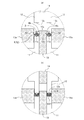
- a temperature sensor according to the first embodiment of the present invention is shown, (a) is a plan view, and (b) is a cross-sectional view taken along the YY line.
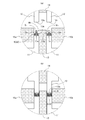
- the connection state between the lead portion and the conductive wire in the temperature sensor is shown, (a) is a side view before welding, (b) is a cross-sectional view along the YY line, and (c) is a side view after welding.
- d) is a cross-sectional view taken along the YY line. It is a block diagram which shows the outline of the resistance welding machine. It is explanatory drawing which shows the connection method of the lead part in the same temperature sensor.
- connection method and connection structure of the lead part (a) shows the state before welding of a lead part, and (b) shows the state after welding of a lead part.
- the relationship between the thickness dimension of the lead portion and the breaking strength is shown, (a) is a photograph showing the joint portion of the lead portion, and (b) shows the relationship between the thickness dimension of the lead portion and the breaking strength. It is a graph.
- a temperature sensor according to a second embodiment of the present invention is shown, (a) is a plan view, and (b) is a cross-sectional view taken along the YY line.
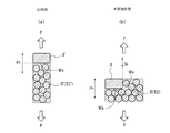
- connection structure of the lead portion of the embodiment is shown in comparison with the comparative example, (a) is an explanatory diagram of the comparative example, and (b) is an explanatory diagram of the embodiment.
- a temperature sensor as an electronic component having a connection structure of a lead portion is shown, (a) is a perspective view, and (b) is a cross-sectional view taken along the YY line.
- FIG. 1 shows a temperature sensor as an electronic component
- FIG. 2 shows a connection state between a lead portion and a conductive wire.
- the temperature sensor 1 as an electronic component includes a thermistor element 2 which is an electronic component element and a lead wire 3 which is a lead portion connected to the thermistor element 2.
- the thermistor element 2 is a temperature-sensitive sintering of a thermistor sintered body, and is manganese (Mn), nickel (Ni), cobalt (Co), iron (Fe), yttrium (Y), chromium (Cr), copper (Cu). ), Zinc (Zn) and other transition metal elements selected from two or more elements, and is composed of an oxide thermistor material containing a composite metal oxide having a crystal structure as a main component. Further, an auxiliary component may be contained for improving the characteristics and the like. The composition and content of the main component and the sub-component can be appropriately determined according to the desired characteristics.
- the thermistor element 2 is covered with a sealing material 4 such as glass. Thereby, the thermistor element 2 can be effectively protected even when the temperature sensor 1 is used in a high temperature environment.
- the lead wire 3 is a pair of conductive round wires having a circular cross section (see FIG. 1B), and is used for electrodes of gold, silver, copper, platinum, etc. formed on the surface of the thermistor element 2. It is electrically connected by welding, soldering, or the like, and is derived from a sealing material 4 such as glass.
- a jumet wire composed of a single conducting wire is preferably used.
- the material of the lead wire 3 is 42 alloy, copper (Cu), iron (Fe), chromium (Cr), nickel (Ni), aluminum (Al), zinc (Zn), titanium (Ti), or at least one of them. Seed-containing alloys can be used.
- the lead wire 3 is electrically connected to the conductive wire 5.
- the conductive wire 5 is an electric wire made of stranded wires coated with an insulating coating 51, and is composed of a plurality of core wires 52, and each core wire 52 is electrically connected to the lead wire 3 by welding.
- FIG. 2A shows a state in which the lead wire 3 is arranged on the line of the conductive wire 5 before the lead wire 3 and the conductive wire 5 are welded. In this state, each core wire 52 of the conductive wire 5 is not welded in advance, and a plurality of core wires 52 that are not integrated are scattered and can be separated.
- FIG. 2B shows a cross section of the lead wire 3 and the conductive wire 5 before being welded.
- FIG. 2C shows a state after the lead wire 3 and the conductive wire 5 are welded by pressurization and heating. The rear end side of the lead wire 3 and the front end side of the conductive wire 5 are welded and joined to form a joint portion 6.
- FIG. 2D schematically shows a cross section of the joint portion 6.
- the lead wire 3 is welded in a state of being inserted into the plurality of core wires 52 of the conductive wire 5.
- a part of the outer circumference in the cross section of the lead wire 3 that is, a state in which the bottom side and both side surfaces excluding the upper part in the cross section of the lead wire 3 are embedded in a plurality of welded core wires 52. It has become.
- the entire peripheral portion of the cross section of the lead wire 3 may be welded in a state of being inserted into the plurality of core wires 52 of the conductive wire 5.
- connection structure of the lead wire 3 as such a lead portion since the lead wire 3 is embedded in the plurality of core wires 52 of the conductive wire 5, the strength of the joint portion 6 against thermal shock and external force is increased. Can be improved.
- the electronic component is not limited to the temperature sensor, and various semiconductor components and the like can be used.
- FIG. 3 is a configuration diagram showing an outline of a resistance welder
- FIG. 4 is an explanatory diagram showing a method of connecting lead portions.
- FIG. 5 is an explanatory view showing the connection method of the lead portion and the connection structure of the lead portion of the present embodiment
- FIG. 6 is a photograph of a sample showing the connection structure of the lead portion of the present embodiment.
- the resistance welder 10 joins a pair of lead wires 3 to a conductive wire 5 by pressurization and heating, and has a lower electrode 11, an upper electrode 12, an insulating member 13 of the lower electrode, and an upper electrode. Insulation member 14, side guide members 15a and 15b are provided.
- the lower electrode 11 is a tungsten electrode, and a flat mounting surface 11a on which the conductive wire 5 is mounted along the axial direction is formed on the upper side.
- the insulating member 13 of the lower electrode is made of a ceramic material, and secures the insulating property of the pair of lower electrodes 11.
- the pair of lower electrodes 11 and the insulating member 13 are integrated to form a fixed side.
- the side guide members 15a and 15b are made of an insulating ceramic material, are arranged on both sides of the lower electrode 11, and can be driven in the lateral direction, that is, in the left-right direction.
- the mounting space Ms is a space for mounting the conductive wire 5 as the material to be welded and the lead wire 3 arranged on the conductive wire 5.
- the mounting space Ms is formed by a flat mounting surface 11a which is a bottom wall, and both side walls Sw and 13a which stand upright from the bottom wall. Therefore, the width dimension of the bottom wall in the mounting space Ms is substantially the same up to the upper side.
- the lower electrode 11, the insulating member 13, and the side guide members 15a and 15b form the mounting space Ms, and the lower form on the fixed side is formed.
- the mounting space Ms is formed in the lower form on the lower electrode 11 side.
- the upper electrode 12 is an anode electrode on the driving side, and is driven in the vertical direction, that is, in the vertical direction.
- the upper electrode 12 is made of tungsten like the lower electrode 11, the insulating member 14 of the upper electrode is made of a ceramic material, and the pair of upper electrodes 12 and the insulating member 14 are integrated.
- a pressure portion having a flat pressure surface 12a is formed on the lower side of the upper electrode 12.
- the width dimension of the pressurizing portion is formed to be slightly smaller than the width dimension of the mounting space Ms, and the pressurizing portion can be inserted into the mounting space Ms.
- the upper electrode 12 and the insulating member 14 form the upper formwork on the drive side.
- FIG. 4 is an enlarged explanatory view showing a main part A of the connection structure of the lead wire 3 in FIG.
- the conductive wire 5 and the lead wire 3 are arranged on the lower electrode 11 side forming the lower form, and pressure is applied on the upper electrode 12 side forming the upper form for welding.
- a conductive wire 5 composed of a plurality of core wires 52 is arranged on the mounting surface 11a of the lower electrode 11.
- each of the core wires 52 of the conductive wire 5 is not welded in advance and is not integrated, so that the plurality of core wires 52 can be separated.
- the side guide members 15a and 15b are located apart from the lower electrode 11.
- the lead wire 3 is placed on the wires of the plurality of core wires 52.
- the side guide members 15a and 15b are driven and moved inward, that is, toward the lower electrode 11.
- the mounting space Ms is formed, and the plurality of core wires 52 of the conductive wire 5 can be separated, but the lateral spread is restricted by the width dimension of the mounting space Ms. Further, of course, the width dimension of the mounting space Ms is wider than the width dimension (diameter dimension) of the cross section of the lead wire 3.
- the upper electrode 12 is driven to descend, and the lead is led by the pressure surface 12a of the upper electrode 12. Pressurize the wire 3 and the conductive wire 5.
- the upper electrode 12 and the lower electrode 11 are energized, and the lead wire 3 and the conductive wire 5 are heated and connected by welding.
- the upper electrode 12 is driven ascending, the side guide members 15a and 15b are driven outward, that is, in the direction away from the lower electrode 11, and the upper electrode 12, the side guide members 15a and 15b are initially driven, respectively. Return to the position of, and take out the welded lead wire 3 and the conductive wire 5.
- the insulating member 13 of the lower electrode, the side guide members 15a and 15b, and the insulating member 14 of the upper electrode are made of a ceramic material. Since the ceramic material has high insulation, pressure resistance, and heat resistance, it can be suitably used for connecting the lead wire 3 as in the present embodiment.
- the lead wire 3 is welded so as to enter into the plurality of core wires 52 of the conductive wire 5.
- each of the core wires 52 of the conductive wire 5 is not welded in advance and the plurality of core wires 52 can be separated from each other, and the spread of the plurality of core wires 52 in the lateral direction is regulated by the mounting space Ms. That is, the relationship between the width dimension of the lead wire 3 (dimension in the radial direction in the cross section) Lw and the width dimension Cw in the cross section of the conductive wire 5 is that the width dimension Lw of the lead wire 3 is larger than the width dimension Cw of the conductive wire 5. This is because the condition of being small and having a relationship of Lw ⁇ Cw (see FIG. 2B) is mainly satisfied.
- the method of connecting the lead portion of the present embodiment includes a lower electrode 11 and an upper electrode 12, a space Ms for placing the material to be welded is formed on the lower electrode 11 side, and the material to be welded is a conductor.
- the lead wire 3 and the conductive wire 5 are pressurized and heated by the lower electrode 11 and the upper electrode 12, and are joined by welding.
- the method of connecting the lead portion of the present embodiment includes an arrangement step of arranging the conductive wire 5 in which the plurality of core wires 52 are not integrated in advance on the lower electrode 11 on the lower mold side, and the plurality of said.
- a mounting step for mounting the lead wire 3 on the core wire 52 a mounting space forming step for driving the side guide members 15a and 15b toward the lower electrode 11 side to form a mounting space Ms, and a mounting space.
- the lead wire 3 placed on the conductive wire 5 and the conductive wire 5 on Ms these are pressurized and heated by the upper electrode 12 on the upper mold side, and the lead wire 3 and the conductive wire 5 are welded together.
- It includes a connection step for connecting by joining, and a take-out step for driving the upper electrode 12 and the side guide members 15a and 15b to open the mounting space Ms and taking out the welded lead wire 3 and the conductive wire 5. ..
- FIG. 5 schematically shows a connection method of the lead portion and a connection structure of the lead portion.
- a conductive wire 5 in which each core wire 52 is not welded in advance is arranged on the lower electrode 11 side, and a lead wire 3 is placed on the conductive wire 5.
- the upper electrode 12 pressurizes and heats the lead wire 3 and the conductive wire 5 by welding. Therefore, the welding process is one time.
- a plurality of core wires in the conductive wire are compacted in advance by welding, and the plurality of core wires are pressed and heat-molded to be solidified and integrated on the lower electrode side. Arrange and place the lead wire on the conductive wire. Next, the lead and the conductive wire are joined by welding by pressurizing and heating with the upper electrode. Therefore, it has undergone two welding steps.
- the plurality of core wires 52 are not compacted by welding in advance and can be separated from each other, and the lead wire 3 is welded on the core wires 52. Therefore, when the lead wire 3 is welded, the lead wire 3 easily enters into the plurality of core wires 52 by pressurization, so that the stress is not concentrated on the lead wire 3 and the plurality of core wires 52 and the lead wire 3 are not concentrated. It can be stressed on a wide surface. Therefore, the amount of deformation of the lead wire 3 becomes small, and the damage can be reduced.
- the damage of the lead wire 3 is small and the lead wire 3 is embedded and welded into the plurality of core wires 52 of the conductive wire 5, the tensile strength of the joint between the conductive wire 5 and the lead wire 3 is increased. Can be increased to improve the joint strength. In addition, it can be expected that the energy of pressurization and heating can be reduced during welding.
- FIG. 6 shows the relationship between the thickness dimension of the lead wire (jumet wire) and the breaking strength
- FIG. 6 (a) shows the joint portion of the lead wire of the present embodiment corresponding to FIG. 5 (b).
- 6 (b) is a graph showing the relationship between the thickness dimension of the lead wire and the breaking strength.
- the lead wire has a wire diameter of ⁇ 0.2. As shown in FIG. 6A, the amount of deformation of the lead wire 3 is small and the damage is small, so that the lead wire 3 enters the plurality of core wires 52 of the conductive wire 5.
- the amount of deformation of the lead wire 3 is small, the thickness dimension t is about 0.15 mm, and as a result of measuring the tensile strength (breaking strength), a breaking strength of 18.1N is obtained. ..
- FIG. 6B shows the results of preparing a plurality of lead wire samples having different thickness dimensions t and measuring the breaking strength thereof.
- the lead wire samples were pressed and crushed to change the thickness dimension t, and the breaking strength of each sample was confirmed by a tensile tester.
- the horizontal axis shows the thickness dimension (mm) of the lead wire
- the vertical axis shows the breaking strength (N).
- the breaking strength of the joint tends to increase as the thickness dimension of the lead wire increases.
- the predetermined breaking strength can be secured if the thickness dimension t is 50% or less as the amount of deformation of the lead wire due to welding.
- the wire diameter (thickness dimension t) of the lead wire material is ⁇ 0.2
- the thickness dimension t after welding is 0.1 mm or more (the amount of deformation of the thickness dimension t is 0.1 mm or less). If so, the breaking strength can be secured. It should be noted that such a confirmation result is the same when the lead portion in the second embodiment described later is a terminal.
- FIG. 7 schematically shows a cross section of a state in which the lead wire 3 at the joint is inserted into the plurality of core wires 52 of the conductive wire 5.
- FIG. 7 (a) to 7 (d) show that a part of the outer periphery of the cross section of the lead wire 3 is the core wire 52, including the case where the lead wire 3 is placed offset from the conductive wire 5. It shows an example of the state of being embedded inside.
- FIG. 7 (a) shows a state in which the lead wire 3 is inserted into the upper corner of the conductive wire 5
- FIG. 7 (b) is a state in which the lead wire 3 is inserted into the side portion of the conductive wire 5
- FIG. 7 (c) is a state in which the lead wire 3 is inserted.
- About half of the lead wire 3 is inserted in the upper part of the wire 5
- FIG. 7D shows a state in which about half of the lead wire 3 is inserted in the upper corner of the conductive wire 5.
- FIG. 7E shows an example of a state in which the entire peripheral portion of the cross section of the lead wire 3 is inserted into the plurality of core wires 52.
- the lead wire 3 is set in advance in the wires of the plurality of core wires 52, specifically in the substantially central portion, and this is arranged on the mounting surface 11a of the lower electrode 11 and joined.
- the same effect as that of the above-described embodiment can be obtained by such a connection structure of the lead wires 3.
- FIGS. 8 to 10 show the same or corresponding parts as those in the first embodiment, and duplicate description will be omitted. Further, in each figure, the scale of each member may be changed as appropriate for the sake of explanation.
- FIG. 8 shows a temperature sensor as an electronic component
- FIG. 9 shows a method of connecting a lead portion.
- FIG. 10 schematically shows a cross section at a joint portion between the lead portion and the conductive wire.
- This embodiment has basically the same configuration as the first embodiment, and a different configuration is the configuration of the lead portion of the temperature sensor.
- the lead portion of the present embodiment is a lead frame-shaped terminal.
- the terminal 3 is a pair of square lines having a conductive cross section and a quadrangular cross section.
- 42 alloy is preferably used as the material of the terminal 3.
- jumet copper (Cu), iron (Fe), chromium (Cr), nickel (Ni), aluminum (Al), zinc (Zn), titanium (Ti) or at least one of them is used.
- the containing alloy can be used.
- an insulating resin such as an epoxy resin having a high heat resistant temperature is used.
- the thermistor element 2 can be effectively protected even when used in a high temperature environment.
- the conductive wire 5 and the terminal 3 are arranged on the lower electrode 11 side forming the lower formwork, and the upper part forming the upper formwork is formed. Welding is performed by applying pressure on the electrode 12 side.
- the conductive wire 5 to which the core wires 52 are not welded in advance is arranged on the mounting surface 11a of the lower electrode 11. Subsequently, the terminal 3 is placed on the plurality of core wires 52. Next, the side guide members 15a and 15b and the upper electrode 12 are driven, the terminal 3 and the conductive wire 5 are pressurized and heated by the upper electrode 12, and the terminal 3 and the conductive wire 5 are joined by welding. In this case, the plurality of core wires 52 of the conductive wires 5 arranged in the mounting space Ms are in a state where they can be separated, but the lateral spread is restricted by the width dimension of the mounting space Ms. Further, of course, the width dimension of the mounting space Ms is wider than the width dimension of the cross section of the terminal 3.
- the terminal 3 is welded in a state of being inserted into the plurality of core wires 52 of the conductive wire 5.
- each of the core wires 52 of the conductive wire 5 is not pre-welded and the plurality of core wires 52 can be separated from each other, and the spread of the plurality of core wires 52 in the lateral direction is regulated by the mounting space Ms. That is, the relationship between the width dimension of the terminal 3 and the width dimension of the conductive wire 5 is mainly due to the fact that the various conditions that the width dimension of the terminal 3 is smaller than the width dimension of the conductive wire 5 are satisfied.
- the same effect as that of the first embodiment can be obtained. That is, the plurality of core wires 52 are not compacted by welding in advance and can be separated from each other, and the terminal 3 is welded on the core wires 52. Therefore, since the terminal 3 easily enters into the plurality of core wires 52 so as to be buried in the plurality of core wires 52, the damage to the terminal 3 can be reduced without the stress being concentrated on the terminal 3. Further, since the terminal 3 is embedded and welded into the plurality of core wires 52 of the conductive wire 5, the tensile strength of the joint portion between the conductive wire 5 and the terminal 3 is increased to improve the joint strength. Can be done.
- FIG. 11 schematically shows a cross section of a state in which the terminal 3 at the joint portion is inserted into the plurality of core wires 52 of the conductive wire 5, and FIG. 12 shows the lead portion of the present embodiment in comparison with the comparative example.
- FIG. 11 (a) to 11 (e) show an example of a state in which a part of the outer circumference of the cross section of the terminal 3 is embedded in the core wire 52.
- FIG. 11A shows a state in which the terminal 3 is inserted into the upper corner of the conductive wire 5
- FIG. 11B shows a state in which the terminal 3 is sandwiched between the conductive wires 5 arranged above and below.
- 11 (c) shows a state in which about half of the terminal 3 is inserted in the upper part of the conductive wire 5
- FIG. 11 (d) shows a state in which more than half of the terminal 3 is inserted in the upper corner of the conductive wire 5.
- FIG. 7 (f) shows an example of a state in which the entire peripheral portion in the cross section of the terminal 3 is inserted into the plurality of core wires 52.
- the terminals 3 are set in advance in the wires of the plurality of core wires 52, and these are arranged on the mounting surface 11a of the lower electrode 11 and joined.
- a plurality of surfaces that is, a plurality of core wires 52 having at least two or more surfaces in the conductive wire 5 It is the welded surface Ws with.
- the conductive wire 5'and the terminal 3' are formed to have the same width dimension. Therefore, the welded surface Ws is one surface.
- FIG. 12 (b) an example (type shown in FIG. 11 (a)) will be taken up and described.
- the two surfaces, the bottom surface side and the one side surface side, are welded surfaces Ws.
- the external force is applied F in the direction perpendicular to the junction of the terminal 3, a problem that in the comparative example is vulnerable to weak peeling the peeling force P F at the weld surface Ws occurs.
- the external force F in the vertical direction in the present embodiment is dispersed to a force S F of the peeling force P F and shear direction, it is possible to obtain the effect of improving the peeling resistance.
- the cross-sectional areas of the conductive wires 5 and 5'of the present embodiment and the comparative example are constant, the height dimension can be made lower in the present embodiment than in the comparative example.
- the temperature sensor 1 can be made low in height.
- the temperature sensor 100 as an electronic component having a lead portion connection structure according to the first embodiment described above will be described with reference to FIG.
- the thermistor element 2 and the lead wire 3 are covered with the coating layer 7, including the joint portion 6 between the lead wire 3 and the conductive wire 5.
- the coating layer 7 covers the portion of the connection structure of the thermistor element 2 and the lead portion. Specifically, the coating layer 7 has an insulating property and has a function of covering the lead wire 3 and the joint portion 6 between the lead wire 3 and the conductive wire 5 and protecting them from the surrounding environment.
- the coating layer 7 is made of a resin material, for example, a fluororesin, and is composed of an inner layer 8 and an outer layer 9.
- the inner layer 8 is formed of a fluororesin FEP (a fluororesin in which tetrafluoroethylene and hexafluoropropylene are jointly combined), and the thermistor element 2 and the like are coated in a state where the FEP is melted and solidified. ..
- FEP fluororesin in which tetrafluoroethylene and hexafluoropropylene are jointly combined
- the inner layer 8 is formed by heating and melting and solidifying a pair of sheet-shaped resin materials (first inner layer material 81 and second inner layer material 82), and is originally a pair (two sheets) of sheet-like material.
- the resin material of No. 1 is melted and integrated into a single layer.
- the thickness dimension of the inner layer 8 is about 1 mm to 1.25 mm.
- the outer layer 9 is formed of a pair of sheet-shaped resin materials, for example, a fluororesin PTFE (ethylene tetrafluoride), and has a first outer layer material 91 and a second outer layer material 92.
- the first outer layer material 91 and the second outer layer material 92 are formed to have a substantially rectangular shape and a flat surface, and have a length dimension of about 22 mm, a width dimension of about 6.6 mm, and a thickness dimension of about 0. It is .25 mm.
- the thickness dimension of the inner layer 8 is about 1 mm to 1.25 mm
- the thickness dimension of the inner layer 8 is larger.
- the thermistor element 2, the lead wire 3, and the joint portion 6 between the lead wire 3 and the conductive wire 5 coated on the inner layer 8 are further coated on the outer layer 9.
- the lead wire 3 and the conductive wire 5 are connected by welding to form the joint portion 6, so that the thickness of the joint portion 6 is increased. Can be thinned. As a result, the thickness dimension of the temperature sensor 100 covered with the coating layer 7 can be reduced, and the temperature measurement accuracy and response performance of the temperature sensor 100 can be improved.
- the conductive wire 5 is connected to a temperature measurement circuit (not shown), it is exposed from one end side of the coating layer 7 and is derived. Therefore, the temperature of the object to be measured can be detected by the temperature measuring circuit based on the change in the resistance value of the thermistor element 2.
- Such a temperature sensor 100 is attached to the object to be measured to detect the temperature.
- the object to be measured is a heat source, and the temperature is detected by bringing the surface of the temperature sensor 100 into contact with the flat plate-shaped portion of the heat source.
- the surfaces of the first outer layer material 91 and the second outer layer material 92 are flat, and the first outer layer material 91 side or the second outer layer material 92 side is used as a temperature detection surface and is brought into contact with the object to be measured. Perform temperature detection.
- the temperature sensor 100 is thinned, the temperature detection surface is flat, and it can be brought into contact with the temperatureed object in a wide contact area, and the heat from the temperatureed object is satisfactorily transferred to the temperature sensor 100, and the thermal response It is fast and can be expected to improve measurement accuracy.
- the covering layer 7 may be provided for the connection structure of the lead portion according to the second embodiment.
Landscapes
- Engineering & Computer Science (AREA)
- Physics & Mathematics (AREA)
- Mechanical Engineering (AREA)
- Nonlinear Science (AREA)
- General Physics & Mathematics (AREA)
- Microelectronics & Electronic Packaging (AREA)
- Electromagnetism (AREA)
- Details Of Resistors (AREA)
- Thermistors And Varistors (AREA)
- Measuring Temperature Or Quantity Of Heat (AREA)
- Manufacturing Of Electrical Connectors (AREA)
- Connections Effected By Soldering, Adhesion, Or Permanent Deformation (AREA)
Priority Applications (4)
| Application Number | Priority Date | Filing Date | Title |
|---|---|---|---|
| JP2022500122A JP7128381B2 (ja) | 2020-03-31 | 2021-03-17 | 電子部品、リード部の接続構造及びリード部の接続方法 |
| CN202180019264.XA CN115315617A (zh) | 2020-03-31 | 2021-03-17 | 电子零件、引线部的连接结构以及引线部的连接方法 |
| US17/909,758 US12510421B2 (en) | 2020-03-31 | 2021-03-17 | Electronic component, lead part connection structure, and lead part connection method |
| DE112021000628.2T DE112021000628T5 (de) | 2020-03-31 | 2021-03-17 | Elektronisches bauteil, leitungsteil-verbindungsstruktur und leitungsteil-verbindungsverfahren |
Applications Claiming Priority (2)
| Application Number | Priority Date | Filing Date | Title |
|---|---|---|---|
| JP2020064180 | 2020-03-31 | ||
| JP2020-064180 | 2020-03-31 |
Publications (1)
| Publication Number | Publication Date |
|---|---|
| WO2021200154A1 true WO2021200154A1 (ja) | 2021-10-07 |
Family
ID=77927853
Family Applications (1)
| Application Number | Title | Priority Date | Filing Date |
|---|---|---|---|
| PCT/JP2021/010810 Ceased WO2021200154A1 (ja) | 2020-03-31 | 2021-03-17 | 電子部品、リード部の接続構造及びリード部の接続方法 |
Country Status (5)
| Country | Link |
|---|---|
| US (1) | US12510421B2 (https=) |
| JP (1) | JP7128381B2 (https=) |
| CN (1) | CN115315617A (https=) |
| DE (1) | DE112021000628T5 (https=) |
| WO (1) | WO2021200154A1 (https=) |
Families Citing this family (1)
| Publication number | Priority date | Publication date | Assignee | Title |
|---|---|---|---|---|
| GB201804622D0 (en) * | 2018-03-22 | 2018-05-09 | Central Glass Co Ltd | Method of producing a vehicle glass assembly |
Citations (3)
| Publication number | Priority date | Publication date | Assignee | Title |
|---|---|---|---|---|
| JPS62265703A (ja) * | 1986-05-14 | 1987-11-18 | 三井金属鉱業株式会社 | サ−ミスタ−とリ−ド線の結合装置 |
| JPH06215851A (ja) * | 1993-01-20 | 1994-08-05 | Toshiba Home Technol Corp | 温度ヒューズの接続方法 |
| WO2019087755A1 (ja) * | 2017-10-30 | 2019-05-09 | Semitec株式会社 | 温度センサ及び温度センサを備えた装置 |
Family Cites Families (7)
| Publication number | Priority date | Publication date | Assignee | Title |
|---|---|---|---|---|
| JP4921425B2 (ja) * | 2008-06-18 | 2012-04-25 | 日立オートモティブシステムズ株式会社 | 導線接続法ならびに接続端子、固定子および回転電機 |
| DE102008045751B4 (de) | 2008-09-04 | 2020-01-30 | Te Connectivity Germany Gmbh | Vorrichtung und Verfahren zum Kompaktierschweißen |
| JP5813599B2 (ja) | 2011-09-07 | 2015-11-17 | 日本特殊陶業株式会社 | センサ及びその製造方法 |
| JP2015232552A (ja) | 2014-05-12 | 2015-12-24 | 日本特殊陶業株式会社 | センサ及びその製造方法 |
| JP2016083671A (ja) | 2014-10-23 | 2016-05-19 | オムロン株式会社 | リード線の接合方法、リード線の接合装置、及び加圧型枠 |
| JP6352557B1 (ja) | 2017-03-24 | 2018-07-04 | 株式会社芝浦電子 | センサ素子、及び、センサ素子の製造方法 |
| JP2018190617A (ja) * | 2017-05-09 | 2018-11-29 | Smk株式会社 | 端子付き電線 |
-
2021
- 2021-03-17 DE DE112021000628.2T patent/DE112021000628T5/de active Pending
- 2021-03-17 US US17/909,758 patent/US12510421B2/en active Active
- 2021-03-17 CN CN202180019264.XA patent/CN115315617A/zh active Pending
- 2021-03-17 WO PCT/JP2021/010810 patent/WO2021200154A1/ja not_active Ceased
- 2021-03-17 JP JP2022500122A patent/JP7128381B2/ja active Active
Patent Citations (3)
| Publication number | Priority date | Publication date | Assignee | Title |
|---|---|---|---|---|
| JPS62265703A (ja) * | 1986-05-14 | 1987-11-18 | 三井金属鉱業株式会社 | サ−ミスタ−とリ−ド線の結合装置 |
| JPH06215851A (ja) * | 1993-01-20 | 1994-08-05 | Toshiba Home Technol Corp | 温度ヒューズの接続方法 |
| WO2019087755A1 (ja) * | 2017-10-30 | 2019-05-09 | Semitec株式会社 | 温度センサ及び温度センサを備えた装置 |
Also Published As
| Publication number | Publication date |
|---|---|
| DE112021000628T5 (de) | 2022-11-24 |
| US12510421B2 (en) | 2025-12-30 |
| JP7128381B2 (ja) | 2022-08-30 |
| US20230093829A1 (en) | 2023-03-30 |
| JPWO2021200154A1 (https=) | 2021-10-07 |
| CN115315617A (zh) | 2022-11-08 |
Similar Documents
| Publication | Publication Date | Title |
|---|---|---|
| US7705265B2 (en) | Method of connecting and structure of connecting electric wire and connection terminal | |
| US10438730B2 (en) | Current sensing resistor and fabrication method thereof | |
| JP6576467B2 (ja) | 電気接続エレメントおよびこれに取り付けられた結合エレメントを備えたガラス板 | |
| JP6352557B1 (ja) | センサ素子、及び、センサ素子の製造方法 | |
| JP7128381B2 (ja) | 電子部品、リード部の接続構造及びリード部の接続方法 | |
| KR101650964B1 (ko) | Ptc 디바이스 및 그것을 갖는 전기 장치 | |
| US10014189B2 (en) | Ceramic package with brazing material near seal member | |
| CN107995775A (zh) | 自带过流保护柔性电路及制造工艺 | |
| JP3454055B2 (ja) | 絶縁電線の接続構造及び接続方法 | |
| JP2814985B2 (ja) | 固体電解コンデンサの製造方法 | |
| US12233491B2 (en) | Welding method for connecting a first connector to a second connector, the use of the welding method, and a welded connection | |
| JP2535489B2 (ja) | 固体電解コンデンサ― | |
| JP3558998B2 (ja) | サーマルヘッド及びその製造法 | |
| KR102527714B1 (ko) | 탄탈륨 캐패시터 및 그의 제조 방법 | |
| JP2013182750A (ja) | 温度ヒューズおよびその製造方法 | |
| JP3459277B2 (ja) | 固体電解コンデンサー | |
| JP4083471B2 (ja) | 薄型ヒュ−ズ及びその製造方法 | |
| TW201003869A (en) | Wire bonding structure, method for bonding a wire and method for manufacturing a semiconductor package | |
| JP3168830B2 (ja) | 半導体型圧力センサ | |
| WO2025040368A1 (en) | Electrical device and method for producing an electrical device | |
| JP5433455B2 (ja) | 抵抗付き温度ヒューズの製造方法 | |
| JP2010140672A (ja) | 接合部構造 | |
| JP2009158624A (ja) | 光半導体装置用パッケージおよびその製造方法 | |
| JPH07254532A (ja) | 半田ワイヤを使用した電子部品 | |
| JPH08102433A (ja) | 固体電解コンデンサー |
Legal Events
| Date | Code | Title | Description |
|---|---|---|---|
| 121 | Ep: the epo has been informed by wipo that ep was designated in this application |
Ref document number: 21779249 Country of ref document: EP Kind code of ref document: A1 |
|
| ENP | Entry into the national phase |
Ref document number: 2022500122 Country of ref document: JP Kind code of ref document: A |
|
| 122 | Ep: pct application non-entry in european phase |
Ref document number: 21779249 Country of ref document: EP Kind code of ref document: A1 |
|
| WWG | Wipo information: grant in national office |
Ref document number: 17909758 Country of ref document: US |