WO2021199477A1 - 電磁波シールド材料およびその製造方法 - Google Patents
電磁波シールド材料およびその製造方法 Download PDFInfo
- Publication number
- WO2021199477A1 WO2021199477A1 PCT/JP2020/041450 JP2020041450W WO2021199477A1 WO 2021199477 A1 WO2021199477 A1 WO 2021199477A1 JP 2020041450 W JP2020041450 W JP 2020041450W WO 2021199477 A1 WO2021199477 A1 WO 2021199477A1
- Authority
- WO
- WIPO (PCT)
- Prior art keywords
- electromagnetic wave
- wave shielding
- shielding material
- carbon nanotubes
- resin
- Prior art date
- Legal status (The legal status is an assumption and is not a legal conclusion. Google has not performed a legal analysis and makes no representation as to the accuracy of the status listed.)
- Ceased
Links
Images


Classifications
-
- C—CHEMISTRY; METALLURGY
- C08—ORGANIC MACROMOLECULAR COMPOUNDS; THEIR PREPARATION OR CHEMICAL WORKING-UP; COMPOSITIONS BASED THEREON
- C08K—Use of inorganic or non-macromolecular organic substances as compounding ingredients
- C08K3/00—Use of inorganic substances as compounding ingredients
- C08K3/02—Elements
- C08K3/04—Carbon
- C08K3/041—Carbon nanotubes
-
- C—CHEMISTRY; METALLURGY
- C01—INORGANIC CHEMISTRY
- C01B—NON-METALLIC ELEMENTS; COMPOUNDS THEREOF; METALLOIDS OR COMPOUNDS THEREOF NOT COVERED BY SUBCLASS C01C
- C01B32/00—Carbon; Compounds thereof
- C01B32/15—Nano-sized carbon materials
- C01B32/158—Carbon nanotubes
- C01B32/168—After-treatment
- C01B32/174—Derivatisation; Solubilisation; Dispersion in solvents
-
- C—CHEMISTRY; METALLURGY
- C08—ORGANIC MACROMOLECULAR COMPOUNDS; THEIR PREPARATION OR CHEMICAL WORKING-UP; COMPOSITIONS BASED THEREON
- C08K—Use of inorganic or non-macromolecular organic substances as compounding ingredients
- C08K3/00—Use of inorganic substances as compounding ingredients
- C08K3/01—Use of inorganic substances as compounding ingredients characterized by their specific function
- C08K3/017—Antistatic agents
-
- C—CHEMISTRY; METALLURGY
- C08—ORGANIC MACROMOLECULAR COMPOUNDS; THEIR PREPARATION OR CHEMICAL WORKING-UP; COMPOSITIONS BASED THEREON
- C08K—Use of inorganic or non-macromolecular organic substances as compounding ingredients
- C08K3/00—Use of inorganic substances as compounding ingredients
- C08K3/02—Elements
- C08K3/04—Carbon
-
- C—CHEMISTRY; METALLURGY
- C08—ORGANIC MACROMOLECULAR COMPOUNDS; THEIR PREPARATION OR CHEMICAL WORKING-UP; COMPOSITIONS BASED THEREON
- C08K—Use of inorganic or non-macromolecular organic substances as compounding ingredients
- C08K7/00—Use of ingredients characterised by shape
- C08K7/02—Fibres or whiskers
-
- C—CHEMISTRY; METALLURGY
- C08—ORGANIC MACROMOLECULAR COMPOUNDS; THEIR PREPARATION OR CHEMICAL WORKING-UP; COMPOSITIONS BASED THEREON
- C08L—COMPOSITIONS OF MACROMOLECULAR COMPOUNDS
- C08L1/00—Compositions of cellulose, modified cellulose or cellulose derivatives
- C08L1/02—Cellulose; Modified cellulose
-
- C—CHEMISTRY; METALLURGY
- C08—ORGANIC MACROMOLECULAR COMPOUNDS; THEIR PREPARATION OR CHEMICAL WORKING-UP; COMPOSITIONS BASED THEREON
- C08L—COMPOSITIONS OF MACROMOLECULAR COMPOUNDS
- C08L1/00—Compositions of cellulose, modified cellulose or cellulose derivatives
- C08L1/08—Cellulose derivatives
-
- C—CHEMISTRY; METALLURGY
- C08—ORGANIC MACROMOLECULAR COMPOUNDS; THEIR PREPARATION OR CHEMICAL WORKING-UP; COMPOSITIONS BASED THEREON
- C08L—COMPOSITIONS OF MACROMOLECULAR COMPOUNDS
- C08L101/00—Compositions of unspecified macromolecular compounds
-
- H—ELECTRICITY
- H05—ELECTRIC TECHNIQUES NOT OTHERWISE PROVIDED FOR
- H05K—PRINTED CIRCUITS; CASINGS OR CONSTRUCTIONAL DETAILS OF ELECTRIC APPARATUS; MANUFACTURE OF ASSEMBLAGES OF ELECTRICAL COMPONENTS
- H05K9/00—Screening of apparatus or components against electric or magnetic fields
-
- H—ELECTRICITY
- H05—ELECTRIC TECHNIQUES NOT OTHERWISE PROVIDED FOR
- H05K—PRINTED CIRCUITS; CASINGS OR CONSTRUCTIONAL DETAILS OF ELECTRIC APPARATUS; MANUFACTURE OF ASSEMBLAGES OF ELECTRICAL COMPONENTS
- H05K9/00—Screening of apparatus or components against electric or magnetic fields
- H05K9/0073—Shielding materials
- H05K9/0081—Electromagnetic shielding materials, e.g. EMI, RFI shielding
Definitions
- the present invention relates to an electromagnetic wave shielding material and a method for manufacturing the same.
- Patent Document 1 describes an electromagnetic wave shielding carbon nanotube polymer composite material containing carbon nanotubes and an elastomer or a polymer.
- the present invention has been made in view of the above problems, and an object of the present invention is to provide an electromagnetic wave shielding material having excellent electromagnetic wave shielding characteristics.
- one aspect of the present invention includes the following configurations.
- ⁇ 4> The electromagnetic wave shielding material according to ⁇ 3>, wherein the transmittance of light having a wavelength of 535 nm is 10% or more.
- ⁇ 5> The electromagnetic wave shielding material according to any one of ⁇ 1> to ⁇ 4>, wherein the resin contains a cellulose derivative.
- ⁇ 6> The electromagnetic wave shielding material according to any one of ⁇ 1> to ⁇ 5>, which further contains a dopant.
- ⁇ 7> A method for producing an electromagnetic wave shielding material, which comprises a step of incinerating the resin by heating a composition containing the resin and carbon nanotubes.
- ⁇ 8> The method for producing an electromagnetic wave shielding material according to ⁇ 7>, wherein the resin contains a cellulose derivative.
- ⁇ 9> The method for producing an electromagnetic wave shielding material according to ⁇ 7> or ⁇ 8>, wherein the composition further contains a dopant.
- an electromagnetic wave shielding material having excellent electromagnetic wave shielding characteristics.
- the electromagnetic wave shielding material according to the embodiment of the present invention contains a resin and carbon nanotubes, and contains 60% by weight or more of the carbon nanotubes.
- the weight ratio of the resin that inhibits conductivity is high, so that sufficient electromagnetic wave shielding characteristics could not be obtained.
- the present inventor has found that a material containing carbon nanotubes in a high weight ratio can be formed to improve the electromagnetic wave shielding property. Further, the present inventor has found that such a material can be realized by heating a composition containing a resin and carbon nanotubes at a high temperature to incinerate the resin as described later. It is surprising that carbon nanotubes can be filled in a high weight ratio as described above even in the form of a thin sheet as described later.
- the "electromagnetic wave shielding material” is obtained by heating a composition containing a resin and carbon nanotubes as described later to incinerate the resin. Therefore, the electromagnetic wave shielding material contains carbon nanotubes in a high weight ratio. That is, the above-mentioned “electromagnetic wave shielding material” does not mean a mere composition, dispersion liquid or coating film before incineration. In other words, the “electromagnetic wave shielding material” is a cured product. Further, it can be said that the "electromagnetic wave shielding material” is a fired body.
- the shape of the electromagnetic wave shielding material is not particularly limited, but it may be in the form of a sheet because it is easy to use for precision equipment and the like.
- the electromagnetic wave shielding material may contain components other than the resin and carbon nanotubes, for example, highly heat-resistant fibers.
- the thickness of the sheet-shaped electromagnetic wave shielding material is preferably 100 nm or more and 100 ⁇ m or less. If the thickness is 100 nm or more, sufficient electromagnetic wave shielding characteristics can be obtained. Further, if the thickness is 100 ⁇ m or less, it is easy to use for precision equipment and the like. When a thin sheet-shaped electromagnetic wave shielding material is obtained from the viewpoint of miniaturization of equipment, the thickness may be 100 nm or more and 2000 nm or less, or 200 nm or more and 1000 nm or less. When a thick sheet-shaped electromagnetic wave shielding material is obtained, the thickness may be 10 ⁇ m or more and 100 ⁇ m or less, or 10 ⁇ m or more and 50 ⁇ m or less. When the thickness is 10 ⁇ m or more, the electromagnetic wave shielding characteristics can be further improved.
- the electromagnetic wave shielding material may be translucent.
- the electromagnetic wave shielding material when it is in the form of a thin sheet, it can be translucent.
- the term "semi-transparent" means that the electromagnetic wave shielding material has a transmittance of light having a wavelength of 535 nm of 10% or more.
- the transmittance of the electromagnetic wave shielding material may be 30% or more, or 50% or more.
- the "electromagnetic wave shielding characteristic” means the effect of shielding or attenuating an electric field wave, a magnetic field wave, or an electromagnetic wave.
- the amount of electromagnetic wave attenuation by the electromagnetic wave shielding material is preferably 5 dB or more, more preferably 10 dB or more, further preferably 15 dB or more, and particularly preferably 20 dB or more.
- the attenuation amount of the electromagnetic wave may be, for example, the attenuation amount measured by the KEC method described in Examples described later when an electric field wave or a magnetic field wave of 1 GHz is applied to the electromagnetic wave shielding material.
- the amount of attenuation of the electromagnetic wave may be the amount of attenuation measured by the waveguide method described in Examples described later when an electromagnetic wave of 40 GHz is applied to the electromagnetic wave shielding material.
- the electromagnetic wave shielding material includes carbon nanotubes.
- the content of carbon nanotubes in 100% by weight of the electromagnetic wave shielding material is preferably 60% by weight or more, more preferably 70% by weight or more, further preferably 80% by weight or more, and 90% by weight. The above is particularly preferable. When the content of carbon nanotubes is in the above range, the electromagnetic wave shielding characteristics are further improved.
- the weight ratio of carbon nanotubes means a value obtained by thermogravimetric analysis shown in Examples described later. The larger the content of carbon nanotubes, the more preferable, but in reality, it may be 99% or less.
- the carbon nanotubes may be single-walled or multi-walled (for example, two-walled, three-walled, four-walled or more multi-walled). Single-walled carbon nanotubes are preferred from the standpoint of good dispersibility.
- the diameter of the carbon nanotubes is preferably 0.5 to 250 nm, more preferably 0.5 to 10 nm, and even more preferably 0.5 to 5 nm.
- the electromagnetic wave shielding material may contain impurities such as iron.
- impurities such as iron.
- commercially available carbon nanotubes and the like may contain such impurities. According to thermogravimetric analysis, it is possible to distinguish between the content of such impurities and the content of carbon nanotubes. Therefore, the above-mentioned content of carbon nanotubes represents the content of carbon nanotubes excluding impurities in the electromagnetic wave shielding material which may contain impurities.
- the amount of impurities contained in the electromagnetic wave shielding material is preferably 20% by weight or less, more preferably 10% by weight or less, and further preferably 5% by weight or less. Most preferably, the electromagnetic wave shielding material does not contain impurities. When the impurities of the electromagnetic wave shielding material are 20% by weight or less, the carbon nanotube content of the electromagnetic wave shielding material increases, and the electromagnetic wave shielding characteristics are improved.
- the resin can act as a dispersant and binder that promotes the dispersion of carbon nanotubes.
- the resin include cellulose derivatives.
- the cellulose derivative include a cellulose derivative having a structure represented by the following formula (1).
- R is independently an H (hydrogen atom), an alkyl group, a hydroxyalkyl group, or an acyl group, except that at least one of R in the formula is an alkyl group or a hydroxy group. It is an alkyl group or an acyl group.
- Examples of the cellulose derivative having an alkyl group include methyl cellulose, ethyl cellulose, propyl cellulose, methyl ethyl cellulose, methyl propyl cellulose, ethyl propyl cellulose and the like.
- the alkyl chain may be a straight chain or a branched chain.
- Examples of the cellulose derivative having a hydroxyalkyl group include hydroxyethyl cellulose, hydroxypropyl cellulose, hydroxypropyl methyl cellulose and the like.
- Examples of cellulose having an acyl group include acetyl cellulose and propionyl cellulose. Since these cellulose derivatives have a hydrophobic group, carbon nanotubes can be dispersed well.
- the cellulose derivative is preferably at least one selected from the group consisting of ethyl cellulose, hydroxypropyl cellulose and acetyl cellulose.
- Ethyl cellulose has a structure in which R is H or C 2 H 5 in the formula (1), and at least one of R is C 2 H 5.
- Hydroxypropyl cellulose has a structure in which R is H or CH 2 CH (OH) CH 3 in the formula (1), and at least one of R is CH 2 CH (OH) CH 3 .
- Acetyl cellulose has a structure in which R is H or COCH 3 in the formula (1), and at least one of R is COCH 3.
- the electromagnetic wave shielding material according to the embodiment of the present invention may further contain a dopant in order to control the electromagnetic wave shielding property.
- the electromagnetic wave shielding property can be controlled by changing the surface resistance of the electromagnetic wave shielding material with the dopant.
- the method for producing an electromagnetic wave shielding material according to an embodiment of the present invention includes a step of ashing a resin by heating a composition containing a resin and carbon nanotubes (a ashing step). As a result, as described above, a material containing carbon nanotubes in a high weight ratio and having excellent electromagnetic wave shielding properties can be obtained. [1. Items already explained in [Electromagnetic wave shield material] will be omitted below.
- the ashing step is a step of ashing the resin by heating the composition containing the resin and carbon nanotubes.
- the ashing step can also be said to be a step of firing the above composition.
- the content of the carbon nanotubes in the composition before incineration is not particularly limited, but it is preferable that the carbon nanotubes are contained in an amount of 0.5% by weight or more in 100% by weight of the composition. It is more preferable that the content is 20% by weight or more.
- the content of the carbon nanotubes may be 50% by weight or less.
- the composition may be, for example, a dispersion liquid or a coating film described later.
- the composition may contain a dopant.
- the heating temperature is not particularly limited as long as it can incinerate the resin, but is, for example, 200 to 1000 ° C, preferably 200 ° C to 800 ° C, and more preferably 200 to 500 ° C.
- the time for heating is also not particularly limited, but is, for example, 1 to 3 hours.
- the method for producing the electromagnetic wave shielding material may include the following dispersion step and / or drying step before the ashing step.
- the dispersion step is a step of dispersing the resin and carbon nanotubes in a dispersion medium to obtain a dispersion liquid.
- Examples of the method for dispersing the resin and carbon nanotubes in the dispersion medium include a method using a homogenizing device.
- Examples of the homogenizer include a stirring homogenizer and an ultrasonic homogenizer. From the viewpoint of more uniform dispersion, it is preferable to use an ultrasonic homogenizer.
- the time for dispersion is not particularly limited, but is, for example, 5 to 60 minutes, preferably 10 to 30 minutes.
- the temperature at which dispersion is performed is also not particularly limited, but is, for example, 5 ° C.
- dispersion medium examples include water and an organic solvent, preferably an organic solvent, and more preferably ether, ester, ketone, alcohol, amine, amide, nitrile and the like.
- ether examples include tetrahydrofuran, 1,4-dioxane, diethyl ether, diethylene glycol dimethyl ether, ethyl carbitol acetate, butyl carbitol acetate, dibenzyl ether, anisole and the like.
- ester examples include ethyl acetate, butyl acetate, dimethyl carbonate, ethyl lactate, butyl lactate, dimethyl phthalate, ⁇ -butyrolactone and the like.
- ketone examples include cyclohexanone, methyl ethyl ketone, acetone, methyl isobutyl ketone, 3-pentanone, acetophenone and the like.
- alcohol examples include methanol, ethanol, isopropanol, 1-butanol, benzyl alcohol, phenol, 2-ethoxyethanol, ethylene glycol and the like.
- dispersion media examples include toluene and a dispersion medium containing a nitrogen atom (1-methyl-2-pyrrolidone, 1-cyclohexyl-2-pyrrolidone, dimethylformamide, N, N'-dimethylpropyleneurea, benzonitrile, acetonitrile).
- Etc. dispersion media containing a sulfur atom (dimethylsulfoxide, etc.) can be mentioned.
- the dispersion medium may be a non-aromatic dispersion medium or a non-amide dispersion medium. Further, the dispersion medium may be a dispersion medium excluding a dispersion medium containing a nitrogen atom and a dispersion medium containing a sulfur atom, or a dispersion medium excluding an aprotic polar solvent.
- the type of the carbon nanotube is not particularly limited, and may be one synthesized based on a known technique or a commercially available one.
- the above-mentioned dopant may be added to the dispersion medium together with the resin and carbon nanotubes.
- the concentration of the dopant in the dispersion is preferably 10 ⁇ g / mL or more and 10000 ⁇ g / mL or less, more preferably 50 ⁇ g / mL or more and 5000 ⁇ g / mL or less, still more preferably 100 ⁇ g / mL or more and 2000 ⁇ g / mL or less.
- the doping amount is 10 ⁇ g / mL or more, the electromagnetic wave shielding property of the electromagnetic wave shielding material is further improved.
- a drying step may be performed after the dispersion step.
- the drying step is a step of removing the dispersion medium from the dispersion liquid.
- the drying method is not particularly limited, and the dispersion may be left at room temperature.
- the dispersion liquid may be applied onto the base material. Then, by drying the applied dispersion liquid, a coating film can be formed on the base material. A sheet-shaped electromagnetic wave shielding material may be obtained by heating this coating film to incinerate the resin. The thickness of the coating film and the sheet-like electromagnetic wave shielding material can be adjusted by applying the dispersion liquid a plurality of times.
- a base material such as glass, transparent ceramics, metal, or plastic film can be used.
- the thickness of the base material is not particularly limited, but is preferably 1 ⁇ m to 1000 ⁇ m.
- the method of applying the dispersion liquid onto the substrate is not particularly limited, but is limited to spin coating, extrusion die coating, blade coating, bar coating, screen printing, stencil printing, roll coating, curtain coating, spray coating, dip coating, and inkjet.
- Known coating methods such as printing and spraying can be used.
- various devices suitable for applying the dispersion liquid can be used, and the present invention is not particularly limited.
- thermogravimetric analysis The amount of carbon nanotubes contained in the sheet was measured by thermogravimetric analysis using a thermogravimetric / differential thermal analyzer TG-DTA2000SE (manufactured by NETZSCH / JAPAN). First, about 10 mg of the sheets prepared in Examples and Comparative Examples were placed on an alumina pan (J156801 manufactured by NETZSCH / JAPAN) and placed in a sample holder of a thermogravimetric / differential thermal analyzer. First, the temperature was raised from room temperature to 600 ° C. under a nitrogen atmosphere, and 600 ° C. was maintained for 10 minutes. Next, the temperature was lowered from 600 ° C. to 300 ° C.
- Transmittance measurement method The transmittance of the sheets of Examples and Comparative Examples was measured using an ultraviolet spectrophotometer UV-2600 (manufactured by Shimadzu Corporation) and an integrating sphere unit ISR-2600 (manufactured by Shimadzu Corporation). The sheet processed to 2.5 cm ⁇ 3 cm was set in the holder of the ultraviolet spectrophotometer. The type of measurement was set to transmittance absorption measurement, and the measurement module was set to spectrum. The measurement conditions are: wavelength range is 185 nm to 900 nm, transmittance measurement wavelength is 535 nm, scan speed is medium speed, sampling pitch is auto sampling pitch, measurement mode is single, photometric value type is transmittance, S / R switching. Was set to standard. The background measurement was performed with air or a coating base material (transparent polyimide film), and then the transmittance was measured.
- the electric field wave shield characteristic and the magnetic field wave shield characteristic of the sheet were measured by the KEC method using an electromagnetic wave shield characteristic measuring device (manufactured by KEC Kansai Electronics Industry Promotion Center).
- the electromagnetic wave shield characteristic measuring device is a device including an electric field wave shield characteristic measuring device 11a and a magnetic field wave shield characteristic measuring device 11b.
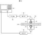
- FIGS. 1 and 2 are diagrams showing the configuration of the system used in the KEC method.
- the system used in the KEC method includes the above-mentioned electromagnetic wave shield characteristic measuring device, a spectrum analyzer 21, an attenuator 22 for attenuating 10 dB, an attenuator 23 for attenuating 3 dB, and a preamplifier 24.
- the electric field wave shield characteristic measuring device 11a is provided with two measuring jigs 13 facing each other. Then, the measurement sample 101 (that is, the sheet) was sandwiched and installed between the two measurement jigs 13.
- the measuring jig 13 is formed to have the same dimensions as the TEM cell (Transverse Electro Magnetic Cell), and the measuring jig 13 has a structure divided into a line-symmetrical shape on a plane perpendicular to the central conductor 14. It has become. However, in order to prevent a short-circuit circuit from being formed by inserting the measurement sample 101, the flat plate-shaped center conductor 14 is arranged with a gap inside each measurement jig 13.
- the magnetic field wave shield characteristic measuring device 11b is provided with two measuring jigs 15 facing each other. Then, the measurement sample 101 was sandwiched and installed between the two measurement jigs 15.
- the magnetic field wave shield characteristic measuring device 11b uses a shielded circular loop antenna 16 as a measuring jig 15 in order to generate an electromagnetic field having a large magnetic field wave component, and combines it with a 90-degree angle metal plate to form a loop antenna.
- the structure is such that the 1/4 part is exposed to the outside.
- the signal output from the spectrum analyzer 21 is input to the measuring jig 13 or the measuring jig 15 on the transmitting side via the attenuator 22. Then, the signal level is measured by the spectrum analyzer 21 after being received by the measuring jig 13 or the measuring jig 15 on the receiving side and amplifying the signal via the attenuator 23 by the preamplifier 24.
- the spectrum analyzer 21 outputs the amount of attenuation when the sample is installed in the electromagnetic wave shield characteristic measuring device, based on the state where the sample is not installed in the electromagnetic wave shield characteristic measuring device.
- the electric field wave shield characteristic and the magnetic field wave shield characteristic of the prepared sample were measured.
- the prepared sample was cut into 15 cm squares and used as a measurement sample. Further, the measurement was carried out in an atmosphere where the frequencies of the electric field wave and the magnetic field wave were 1 GHz, the temperature was 25 ° C., and the relative humidity was 30 to 50%.
- FIG. 3 is a diagram showing a configuration of a system used in the waveguide method.
- the system used in the waveguide method includes a network analyzer 41, a coaxial waveguide adapter 31, and a waveguide sample holder 32.
- An E8631A manufactured by KEYSIGHT was used as the network analyzer 41.
- the above system is provided with two coaxial waveguide adapters 31 facing each other.
- a waveguide sample holder 32 having a thickness of 3 mm and a measurement sample 101 were installed inside the waveguide sample holder 32.
- R-281A (manufactured by KEY SIGHT) was used for the coaxial waveguide adapter 31, and WR-28 (manufactured by Kanto Electronics Applied Development Co., Ltd.) was used for the waveguide sample holder 32.
- the signal output from the network analyzer 41 is input to the coaxial waveguide adapter 31 on the transmitting side. Then, it is received by the coaxial waveguide adapter 31 on the receiving side, and the signal level is measured by the network analyzer 41.
- the network analyzer 41 outputs the amount of attenuation when the sample is installed in the system based on the state in which the sample is not installed in the system.
- the electromagnetic wave shield characteristics were measured using this system.
- the measurement was performed in an atmosphere where the frequency of the electromagnetic wave was 40 GHz, the temperature was 25 ° C., and the relative humidity was 30 to 50%.
- Example 1 A dispersion was obtained by adding 200 mg of carbon nanotubes (TUBALL manufactured by OCSiAl) to a solution prepared by adding 800 mg of ethyl cellulose to 200 mL of tetrahydrofuran and dispersing by an ultrasonic dispersion device. Using UP200Ht (manufactured by Hielscher) as an ultrasonic disperser, dispersion was performed at a dispersion time of 375 seconds, an output of 200 W, and a frequency of 26 kHz.
- UP200Ht manufactured by Hielscher
- the obtained dispersion liquid was applied onto a substrate using an automatic film applicator BEVS1818 (manufactured by BEVS) to obtain a coating film.
- BEVS1818 manufactured by BEVS
- a polyimide film was used as the base material.
- the coating film was repeatedly coated 5 times with a 20 MIL applicator to prepare a coating film having a thickness of 30 ⁇ m. Drying after coating was carried out at room temperature for 1 day.
- the dried coating film was fired using a high-performance muffle furnace HPM-ON (manufactured by AS ONE) to obtain the sheet (electromagnetic wave shielding material) of Example 1.
- the firing time was 60 minutes and the temperature was 300 ° C.
- Example 2 A dispersion was prepared in the same manner as in Example 1 except that 200 mg of KTFSI was added as a dopant to the dispersion.
- Example 2 Using the obtained dispersion liquid, the coating film of Example 2 was obtained in the same manner as in Example 1 except that the number of recoating was 4 times and the drying time was 300 minutes.
- the coating film was heated from room temperature to 300 ° C. for 120 minutes using the same apparatus as in Example 1, and further fired at 300 ° C. for 60 minutes to obtain a sheet of Example 2.
- Example 3 A dispersion was prepared in the same manner as in Example 1 except that the dispersion was 100 mL of tetrahydrofuran, 20.2 mg of carbon nanotubes, and 2 g of ethyl cellulose, and the dispersion time was 388 seconds.
- Example 2 Using the obtained dispersion liquid, a coating film was obtained in the same manner as in Example 1 except that the applicator was 0.5 MIL and the drying time was 10 minutes.
- the coating film was heated from room temperature to 260 ° C. for 60 minutes using the same apparatus as in Example 1, and further fired at 260 ° C. for 90 minutes to obtain a sheet of Example 3.
- Example 4 As carbon nanotubes, eDIPS (EC1.5-P) (manufactured by Meijo Nanocarbon Co., Ltd.) was used to obtain a dispersion liquid in the same manner as in Example 3 except that the dispersion time was 401 seconds. A coating film was obtained in the same manner as in Example 3 except that the obtained dispersion liquid was used. The coating film was fired in the same manner as in Example 3 to obtain a sheet of Example 4.
- Example 1 A dispersion liquid was prepared in the same manner as in Example 1 by adding 4 mg of the same carbon nanotubes as in Example 1 to a solution in which 400 mg of ethyl cellulose was added to 20 mL of tetrahydrofuran.
- the dispersion device was changed to an ultrasonic homogenizer Q125 (manufactured by QSONICA), and dispersion was performed at a dispersion time of 600 seconds, an output of 125 W, and a frequency of 20 kHz.
- Example 1 Using the obtained dispersion liquid, a sheet of Comparative Example 1 was obtained in the same manner as in Example 1 except that it was repeatedly coated 7 times with a 0.5 MIL applicator. No firing was performed.
- Examples 1 to 4 having a carbon nanotube content of 60% by weight or more were subjected to any of 1 GHz electric field wave, 1 GHz magnetic field wave, and 40 GHz electromagnetic wave as compared with Comparative Example 1. It can be seen that it shows a high shielding effect.
- Examples 3 and 4 have transparency to light having a wavelength of 535 nm because the thickness is 1 ⁇ m or less.
- the present invention can be suitably used as an electromagnetic wave shielding material.
Landscapes
- Chemical & Material Sciences (AREA)
- Organic Chemistry (AREA)
- Health & Medical Sciences (AREA)
- Chemical Kinetics & Catalysis (AREA)
- Medicinal Chemistry (AREA)
- Polymers & Plastics (AREA)
- Engineering & Computer Science (AREA)
- Materials Engineering (AREA)
- Nanotechnology (AREA)
- Microelectronics & Electronic Packaging (AREA)
- Physics & Mathematics (AREA)
- Electromagnetism (AREA)
- Inorganic Chemistry (AREA)
- Shielding Devices Or Components To Electric Or Magnetic Fields (AREA)
Abstract
電磁波シールド特性に優れた電磁波シールド材料を提供する。本発明の一実施形態に係る電磁波シールド材料は、樹脂およびカーボンナノチューブを含み、当該カーボンナノチューブを60重量%以上含む。
Description
本発明は電磁波シールド材料およびその製造方法に関する。
近年、スマートフォンおよびタブレット型情報端末には、大容量のデータを高速に伝送する性能が求められている。また、大容量のデータを高速伝送するためには高周波信号を用いる必要がある。しかし、高周波信号を用いると、プリント配線板に設けられた信号回路から電磁波ノイズが発生し、周辺機器が誤動作しやすくなる。そこで、このような誤動作を防止するために、プリント配線板を電磁波からシールドすることが重要となる。
例えば、特許文献1にはカーボンナノチューブとエラストマーもしくは高分子とを含む電磁波遮蔽カーボンナノチューブ高分子複合材料が記載されている。
しかしながら、上述のような従来技術は、電磁波シールド特性の観点から未だ改善の余地があった。本発明は上記問題点を鑑みなされたものであり、その目的は電磁波シールド特性に優れた電磁波シールド材料を提供することにある。
上記の課題を解決するために、本発明者らは鋭意検討した結果、カーボンナノチューブの含有量を高めることにより、従来の電磁波シールド材料よりも電磁波シールド特性を向上できることを見出し、本発明を完成させるに至った。すなわち、本発明の一態様は以下の構成を含む。
<1>樹脂およびカーボンナノチューブを含み、当該カーボンナノチューブを60重量%以上含む、電磁波シールド材料。
<2>シート状である、<1>に記載の電磁波シールド材料。
<3>厚みが100nm以上、100μm以下である、<2>に記載の電磁波シールド材料。
<4>535nmの波長の光の透過率が10%以上である、<3>に記載の電磁波シールド材料。
<5>上記樹脂はセルロース誘導体を含む、<1>~<4>のいずれか1つに記載の電磁波シールド材料。
<6>ドーパントをさらに含むことを特徴とする、<1>~<5>のいずれか1つに記載の電磁波シールド材料。
<7>樹脂およびカーボンナノチューブを含む組成物を加熱することにより樹脂を灰化させる工程を含む、電磁波シールド材料の製造方法。
<8>上記樹脂はセルロース誘導体を含む、<7>に記載の電磁波シールド材料の製造方法。
<9>上記組成物はドーパントをさらに含む、<7>または<8>に記載の電磁波シールド材料の製造方法。
<1>樹脂およびカーボンナノチューブを含み、当該カーボンナノチューブを60重量%以上含む、電磁波シールド材料。
<2>シート状である、<1>に記載の電磁波シールド材料。
<3>厚みが100nm以上、100μm以下である、<2>に記載の電磁波シールド材料。
<4>535nmの波長の光の透過率が10%以上である、<3>に記載の電磁波シールド材料。
<5>上記樹脂はセルロース誘導体を含む、<1>~<4>のいずれか1つに記載の電磁波シールド材料。
<6>ドーパントをさらに含むことを特徴とする、<1>~<5>のいずれか1つに記載の電磁波シールド材料。
<7>樹脂およびカーボンナノチューブを含む組成物を加熱することにより樹脂を灰化させる工程を含む、電磁波シールド材料の製造方法。
<8>上記樹脂はセルロース誘導体を含む、<7>に記載の電磁波シールド材料の製造方法。
<9>上記組成物はドーパントをさらに含む、<7>または<8>に記載の電磁波シールド材料の製造方法。
本発明の一態様によれば、電磁波シールド特性に優れる電磁波シールド材料を提供できる。
〔1.電磁波シールド材料〕
本発明の一実施形態に係る電磁波シールド材料は、樹脂およびカーボンナノチューブを含み、当該カーボンナノチューブを60重量%以上含む。
本発明の一実施形態に係る電磁波シールド材料は、樹脂およびカーボンナノチューブを含み、当該カーボンナノチューブを60重量%以上含む。
従来技術では導電性を阻害する樹脂の重量比が高いため、十分な電磁波シールド特性を得ることができなかった。これに対し、本発明者は、カーボンナノチューブを高い重量比で含有する材料を形成し、電磁波シールド特性を向上できることを見出した。また、本発明者は、後述のように樹脂およびカーボンナノチューブを含む組成物を高温で加熱して樹脂を灰化することにより、このような材料を実現できることを見出した。なお、後述のような薄いシート状であっても、上述のようにカーボンナノチューブを高い重量比で充填できることは、驚くべきことである。
なお、本明細書において、「電磁波シールド材料」は、後述のように樹脂とカーボンナノチューブとを含む組成物を加熱し、樹脂を灰化することにより得られる。それゆえに当該電磁波シールド材料は、高い重量比でカーボンナノチューブを含有している。つまり、上記「電磁波シールド材料」は、灰化する前の単なる組成物、分散液または塗膜を意味するわけではない。換言すれば、「電磁波シールド材料」は硬化物である。また、「電磁波シールド材料」は、焼成体であるとも言える。
電磁波シールド材料の形状は、特に限定されないが、精密機器等に用いやすいことから、例えば、シート状であってもよい。なお、電磁波シールド材料は、樹脂およびカーボンナノチューブ以外の成分、例えば高耐熱繊維を含んでいてもよい。
シート状の電磁波シールド材料の厚みは、100nm以上、100μm以下であることが好ましい。厚みが100nm以上であれば十分な電磁波シールド特性が得られる。また、厚みが100μm以下であれば、精密機器等に用いやすい。機器の小型化の観点から薄いシート状の電磁波シールド材料を得る場合は、厚みは100nm以上、2000nm以下であってもよく、200nm以上、1000nm以下であってもよい。厚いシート状の電磁波シールド材料を得る場合は、厚みは10μm以上、100μm以下でもあってもよく、10μm以上、50μm以下であってもよい。厚みが10μm以上であれば、電磁波シールド特性をより向上させることができる。
電磁波シールド材料は、半透明であってもよい。例えば、電磁波シールド材料が薄いシート状である場合、半透明になり得る。本明細書中において、「半透明」とは、電磁波シールド材料の、波長535nmの光の透過率が10%以上であることを意味する。電磁波シールド材料の透過率は30%以上であってもよく、50%以上であってもよい。
本明細書において「電磁波シールド特性」とは、電界波、磁界波または電磁波を遮蔽または減衰させる効果を意味する。上記電磁波シールド材料による電磁波の減衰量は、好ましくは5dB以上であり、より好ましくは10dB以上であり、さらに好ましくは15dB以上であり、特に好ましくは20dB以上である。上記電磁波の減衰量は、例えば、1GHzの電界波または磁界波を当該電磁波シールド材料に与えた場合に、後述の実施例に記載のKEC法で測定した減衰量であってもよい。または、上記電磁波の減衰量は、40GHzの電磁波を当該電磁波シールド材料に与えた場合に、後述の実施例に記載の導波管法で測定した減衰量であってもよい。電磁波の減衰量は大きいほど好ましい。
<1-1.カーボンナノチューブ>
上記電磁波シールド材料はカーボンナノチューブを含む。電磁波シールド材料100重量%中のカーボンナノチューブの含有量は、60重量%以上であることが好ましく、70重量%以上であることがより好ましく、80重量%以上であることがさらに好ましく、90重量%以上であることが特に好ましい。カーボンナノチューブの含有量が上記範囲であれば、電磁波シールド特性がより向上する。本明細書において、カーボンナノチューブの重量比は、後述の実施例に示す熱重量分析によって得られた値を意味する。カーボンナノチューブの含有量は大きければ大きい程好ましいが、現実的には99%以下であってもよい。
上記電磁波シールド材料はカーボンナノチューブを含む。電磁波シールド材料100重量%中のカーボンナノチューブの含有量は、60重量%以上であることが好ましく、70重量%以上であることがより好ましく、80重量%以上であることがさらに好ましく、90重量%以上であることが特に好ましい。カーボンナノチューブの含有量が上記範囲であれば、電磁波シールド特性がより向上する。本明細書において、カーボンナノチューブの重量比は、後述の実施例に示す熱重量分析によって得られた値を意味する。カーボンナノチューブの含有量は大きければ大きい程好ましいが、現実的には99%以下であってもよい。
カーボンナノチューブは、単層であってもよく、多層(例えば、2層、3層、4層またはそれよりも多層)であってもよい。良好な分散性の観点から、単層カーボンナノチューブが好ましい。
カーボンナノチューブの直径は、分散性の観点から、0.5~250nmであることが好ましく、0.5~10nmであることがより好ましく、0.5~5nmであることがさらに好ましい。
電磁波シールド材料は、鉄等の不純物を含んでいてもよい。例えば市販のカーボンナノチューブ等にはこのような不純物が含まれている場合がある。なお、熱重量分析によればこのような不純物の含有量とカーボンナノチューブの含有量とを区別可能である。従って、上述のカーボンナノチューブの含有量は、不純物を含み得る電磁波シールド材料中の、不純物を除いたカーボンナノチューブの含有量を表す。
電磁波シールド材料に含有される不純物は20重量%以下であることが好ましく、10重量%以下であることがより好ましく、5重量%以下であることがさらに好ましい。電磁波シールド材料は、不純物を含有しないことが最も好ましい。電磁波シールド材料の不純物が20重量%以下であれば、電磁波シールド材料のカーボンナノチューブ含有量が増加し、電磁波シールド特性が向上する。
<1-2.樹脂>
樹脂は、カーボンナノチューブの分散を促進する分散剤およびバインダとして作用し得る。樹脂としては、セルロース誘導体等が挙げられる。セルロース誘導体としては、下記式(1)で表される構造を有するセルロース誘導体が挙げられる。
樹脂は、カーボンナノチューブの分散を促進する分散剤およびバインダとして作用し得る。樹脂としては、セルロース誘導体等が挙げられる。セルロース誘導体としては、下記式(1)で表される構造を有するセルロース誘導体が挙げられる。

上記式(1)中、nは繰り返し数を表す。n=5~5000であり、好ましくは10~1000であり、より好ましくは50~500である。
上記式(1)中、Rはそれぞれ独立して、H(水素原子)、アルキル基、ヒドロキシアルキル基、またはアシル基であり、ただし、式中のRの少なくともいずれか1つはアルキル基、ヒドロキシアルキル基、またはアシル基である。
アルキル基を有するセルロース誘導体としては、メチルセルロース、エチルセルロース、プロピルセルロース、メチルエチルセルロース、メチルプロピルセルロース、エチルプロピルセルロース等が挙げられる。アルキル鎖は直鎖でもよく、分岐鎖でもよい。ヒドロキシアルキル基を有するセルロース誘導体としては、ヒドロキシエチルセルロース、ヒドロキシプロピルセルロース、ヒドロキシプロピルメチルセルロース等が挙げられる。アシル基を有するセルロースとしては、アセチルセルロース、プロピオニルセルロース等が挙げられる。これらのセルロース誘導体は、疎水基を有するため、カーボンナノチューブを良好に分散させることができる。
中でも、上記セルロース誘導体は、エチルセルロース、ヒドロキシプロピルセルロースおよびアセチルセルロースからなる群より選択される少なくとも1種であることが好ましい。エチルセルロースは、式(1)中、RがHまたはC2H5であり、Rの少なくとも1つはC2H5である構造を有する。ヒドロキシプロピルセルロースは、式(1)中、RがHまたはCH2CH(OH)CH3であり、Rの少なくとも1つはCH2CH(OH)CH3である構造を有する。アセチルセルロースは、式(1)中、RがHまたはCOCH3であり、Rの少なくとも1つはCOCH3である構造を有する。
また、上記樹脂は1種類のみを用いてもよく、2種類以上の樹脂を任意に組み合わせた混合物を用いてもよい。
<1-3.ドーパント>
本発明の一実施形態に係る電磁波シールド材料は、電磁波シールド特性を制御するためにさらにドーパントを含んでいてもよい。ドーパントによって、電磁波シールド材料の表面抵抗を変化させることで、電磁波シールド特性を制御することができる。
本発明の一実施形態に係る電磁波シールド材料は、電磁波シールド特性を制御するためにさらにドーパントを含んでいてもよい。ドーパントによって、電磁波シールド材料の表面抵抗を変化させることで、電磁波シールド特性を制御することができる。
ドーパントとしては例えば、ビス(トリフルオロメタンスルホニル)アミンアニオン(TFSI-)、例えば、チオシアン酸イオン(SCN-)、過塩素酸イオン(ClO4
-)、過マンガン酸イオン(MnO4
-)、テトラフルオロホウ酸イオン(BF4
-)、ヨウ素酸イオン(IO3
-)、ヘキサフルオロリン酸イオン(PF6
-)、トリフルオロメタンスルホナートアニオン(TfO-)、ヨウ化物イオン(I-)、臭化物イオン(Br-)、塩化物イオン(Cl-)、硝酸イオン(NO3
-)またはトシラートイオン(Tos-)の水素酸および塩が挙げられる。塩としては、銀塩、銅塩、カリウム塩が挙げられる。
〔2.電磁波シールド材料の製造方法〕
本発明の一実施形態に係る電磁波シールド材料の製造方法は、樹脂およびカーボンナノチューブを含む組成物を加熱することにより樹脂を灰化させる工程(灰化工程)を含む。これにより、上述のようにカーボンナノチューブを高い重量比で含有し、優れた電磁波シールド特性を有する材料を得ることができる。〔1.電磁波シールド材料〕で既に説明した事項については、以下では説明を省略する。
本発明の一実施形態に係る電磁波シールド材料の製造方法は、樹脂およびカーボンナノチューブを含む組成物を加熱することにより樹脂を灰化させる工程(灰化工程)を含む。これにより、上述のようにカーボンナノチューブを高い重量比で含有し、優れた電磁波シールド特性を有する材料を得ることができる。〔1.電磁波シールド材料〕で既に説明した事項については、以下では説明を省略する。
<2-1.灰化工程>
灰化工程は、樹脂およびカーボンナノチューブを含む組成物を加熱することにより樹脂を灰化させる工程である。灰化工程は、上記組成物を焼成する工程とも言える。これにより、樹脂の大部分を揮発させることができるため、カーボンナノチューブを高い重量比で含有する材料を得ることができる。それゆえ、灰化前の組成物のカーボンナノチューブの含有量は特に限定されないが、上記組成物100重量%中、上記カーボンナノチューブは0.5重量%以上含まれることが好ましく、5重量%以上含まれることがより好ましく、20重量%以上含まれることがさらに好ましい。上記カーボンナノチューブの含有量は50重量%以下であってもよい。上記組成物は、例えば、後述の分散液または塗膜であってもよい。上記組成物は、ドーパントを含んでいてもよい。
灰化工程は、樹脂およびカーボンナノチューブを含む組成物を加熱することにより樹脂を灰化させる工程である。灰化工程は、上記組成物を焼成する工程とも言える。これにより、樹脂の大部分を揮発させることができるため、カーボンナノチューブを高い重量比で含有する材料を得ることができる。それゆえ、灰化前の組成物のカーボンナノチューブの含有量は特に限定されないが、上記組成物100重量%中、上記カーボンナノチューブは0.5重量%以上含まれることが好ましく、5重量%以上含まれることがより好ましく、20重量%以上含まれることがさらに好ましい。上記カーボンナノチューブの含有量は50重量%以下であってもよい。上記組成物は、例えば、後述の分散液または塗膜であってもよい。上記組成物は、ドーパントを含んでいてもよい。
加熱を行う温度は上記樹脂を灰化させることができる温度であれば特に限定されないが、例えば200~1000℃、好ましくは200℃~800℃、より好ましくは200~500℃である。加熱を行う時間も特に限定されないが、例えば1~3時間である。
なお、上記電磁波シールド材料の製造方法は、灰化工程の前に下記の分散工程および/または乾燥工程を含んでいてもよい。
<2-2.分散工程>
分散工程は、樹脂およびカーボンナノチューブを分散媒中に分散させて分散液を得る工程である。樹脂およびカーボンナノチューブを分散媒中に分散させる方法としては、例えば、均質化装置を用いる方法が挙げられる。均質化装置としては、例えば、撹拌ホモジナイザーおよび超音波ホモジナイザーなどが挙げられる。より均一に分散させる観点から、超音波ホモジナイザーを用いることが好ましい。
分散工程は、樹脂およびカーボンナノチューブを分散媒中に分散させて分散液を得る工程である。樹脂およびカーボンナノチューブを分散媒中に分散させる方法としては、例えば、均質化装置を用いる方法が挙げられる。均質化装置としては、例えば、撹拌ホモジナイザーおよび超音波ホモジナイザーなどが挙げられる。より均一に分散させる観点から、超音波ホモジナイザーを用いることが好ましい。
分散を行う時間は特に限定されないが、例えば5~60分間、好ましくは10~30分間である。分散を行う温度も特に限定されないが、例えば5℃である。
分散媒としては例えば、水および有機溶媒が挙げられ、好ましくは有機溶媒であり、より好ましくはエーテル、エステル、ケトン、アルコール、アミン、アミド、ニトリル等である。
エーテルとしては、例えば、テトラヒドロフラン、1,4-ジオキサン、ジエチルエーテル、ジエチレングリコールジメチルエーテル、エチルカルビトールアセテート、ブチルカルビトールアセテート、ジベンジルエーテル、アニソール等が挙げられる。
エステルとしては、例えば、酢酸エチル、酢酸ブチル、炭酸ジメチル、乳酸エチル、乳酸ブチル、フタル酸ジメチル、γ-ブチロラクトン等が挙げられる。
ケトンとしては、例えば、シクロヘキサノン、メチルエチルケトン、アセトン、メチルイソブチルケトン、3-ペンタノン、アセトフェノン等が挙げられる。
アルコールとしては、メタノール、エタノール、イソプロパノール、1-ブタノール、ベンジルアルコール、フェノール、2-エトキシエタノール、エチレングリコール等が挙げられる。
その他の分散媒としては、例えば、トルエン、窒素原子を含む分散媒(1-メチル-2-ピロリドン、1-シクロヘキシル-2-ピロリドン、ジメチルホルムアミド、N,N’-ジメチルプロピレン尿素、ベンゾニトリル、アセトニトリル等)、硫黄原子を含む分散媒(ジメチルスルホキシド等)が挙げられる。
分散媒は、非芳香族系分散媒または非アミド系分散媒であってもよい。また、分散媒は、窒素原子を含む分散媒および硫黄原子を含む分散媒を除く分散媒、あるいは非プロトン性極性溶媒を除く分散媒であってもよい。
なお、上記カーボンナノチューブの種類は、特に限定されず、公知の技術に基づいて合成されたものであってもよく、市販されているものであってもよい。
上述のドーパントは、樹脂およびカーボンナノチューブとともに分散媒中に添加されてもよい。分散液中のドーパントの濃度は、好ましくは10μg/mL以上、10000μg/mL以下、より好ましくは50μg/mL以上、5000μg/mL以下、さらに好ましくは100μg/mL以上、2000μg/mL以下である。ドーピング量が10μg/mL以上であれば、電磁波シールド材料の電磁波シールド特性がより向上する。
<2-3.乾燥工程>
分散工程の後に乾燥工程を行ってもよい。乾燥工程は、上記分散液から分散媒を除去する工程である。乾燥方法は特に限定されず、分散液を室温で放置してもよい。
分散工程の後に乾燥工程を行ってもよい。乾燥工程は、上記分散液から分散媒を除去する工程である。乾燥方法は特に限定されず、分散液を室温で放置してもよい。
ここで、分散液を基材上に塗布してもよい。その後、塗布した分散液を乾燥させることで、基材上に塗膜を形成することができる。この塗膜を加熱して樹脂を灰化することにより、シート状の電磁波シールド材料を得てもよい。なお、分散液を複数回塗布することにより、塗膜およびシート状の電磁波シールド材料の厚みを調整することもできる。
基材としては、ガラス、透明セラミックス、金属、プラスチックフィルム等の基材を用いることができる。基材の厚さは、特に限定されないが、1μm~1000μmが好ましい。
分散液を基材上に塗布する方法としては、特に限定されないが、スピンコート、エクストルージョンダイコート、ブレードコート、バーコート、スクリーン印刷、ステンシル印刷、ロールコート、カーテンコート、スプレーコート、ディップコート、インクジェット印刷、ディスペンス等の公知の塗布方法を用いることができる。また、分散液の塗布に適した各種装置を用いることができ、特に限定されない。
本発明は上述した各実施形態に限定されるものではなく、請求項に示した範囲で種々の変更が可能であり、異なる実施形態にそれぞれ開示された技術的手段を適宜組み合わせて得られる実施形態についても本発明の技術的範囲に含まれる。
以下、実施例に基づいて本発明をより詳細に説明するが、本発明は以下の実施例に限定されるものではない。
〔熱重量分析〕
熱重量・示差熱分析装置TG-DTA2000SE(NETZSCH・JAPAN製)を用いた熱重量分析によってシートに含まれるカーボンナノチューブの量を測定した。まず実施例および比較例で作製したシートを10mg程度、アルミナパン(NETZSCH・JAPAN製 J1560181)に載せ、熱重量・示差熱分析装置の試料ホルダ内に設置した。最初に窒素雰囲気下、室温から600℃に昇温して、600℃を10分維持した。次に窒素雰囲気下で600℃から300℃に降温して、300℃を10分維持した。最後に空気雰囲気下、300℃から1000℃に昇温して、1000℃を10分維持した。なお、温度の変更速度は10℃/分であり、使用した窒素および空気の流量は150mL/分に設定した。その後、得られた結果を解析ソフトウェア(NETZSCH・JAPAN製)によって解析することでシート中のカーボンナノチューブの含有量のデータを得た。
熱重量・示差熱分析装置TG-DTA2000SE(NETZSCH・JAPAN製)を用いた熱重量分析によってシートに含まれるカーボンナノチューブの量を測定した。まず実施例および比較例で作製したシートを10mg程度、アルミナパン(NETZSCH・JAPAN製 J1560181)に載せ、熱重量・示差熱分析装置の試料ホルダ内に設置した。最初に窒素雰囲気下、室温から600℃に昇温して、600℃を10分維持した。次に窒素雰囲気下で600℃から300℃に降温して、300℃を10分維持した。最後に空気雰囲気下、300℃から1000℃に昇温して、1000℃を10分維持した。なお、温度の変更速度は10℃/分であり、使用した窒素および空気の流量は150mL/分に設定した。その後、得られた結果を解析ソフトウェア(NETZSCH・JAPAN製)によって解析することでシート中のカーボンナノチューブの含有量のデータを得た。
〔透過率測定方法〕
紫外分光光度計UV-2600(島津製作所製)および積分球ユニットISR-2600(島津製作所製)を用いて実施例および比較例のシートの透過率を測定した。2.5cm×3cmに加工したシートを、紫外分光光度計のホルダにセットした。測定の種類を透過率吸収測定、測定モジュールをスペクトルに設定した。また、測定条件は、波長範囲は185nm~900nm、透過率測定波長は535nm、スキャンスピードは中速、サンプリングピッチはオートサンプリングピッチ、測定モードはシングル、測光値の種類は透過率、S/R切替は標準に設定した。なお、バックグラウンド測定を空気またはコーティング基材(透明ポリイミドフィルム)で行ってから、透過率の測定を行った。
紫外分光光度計UV-2600(島津製作所製)および積分球ユニットISR-2600(島津製作所製)を用いて実施例および比較例のシートの透過率を測定した。2.5cm×3cmに加工したシートを、紫外分光光度計のホルダにセットした。測定の種類を透過率吸収測定、測定モジュールをスペクトルに設定した。また、測定条件は、波長範囲は185nm~900nm、透過率測定波長は535nm、スキャンスピードは中速、サンプリングピッチはオートサンプリングピッチ、測定モードはシングル、測光値の種類は透過率、S/R切替は標準に設定した。なお、バックグラウンド測定を空気またはコーティング基材(透明ポリイミドフィルム)で行ってから、透過率の測定を行った。
〔KEC法による電磁波シールド特性の測定〕
シートの電界波シールド特性および磁界波シールド特性について、電磁波シールド特性測定装置(一般社団法人KEC関西電子工業振興センター製)を用いたKEC法により測定した。上記電磁波シールド特性測定装置は、電界波シールド特性測定装置11aと磁界波シールド特性測定装置11bからなる装置である。
シートの電界波シールド特性および磁界波シールド特性について、電磁波シールド特性測定装置(一般社団法人KEC関西電子工業振興センター製)を用いたKEC法により測定した。上記電磁波シールド特性測定装置は、電界波シールド特性測定装置11aと磁界波シールド特性測定装置11bからなる装置である。
図1~図2は、KEC法で用いられるシステムの構成を示す図である。KEC法で用いられるシステムは、上述の電磁波シールド特性測定装置と、スペクトラムアナライザ21と、10dBの減衰を行うアッテネータ22と、3dBの減衰を行うアッテネータ23と、プリアンプ24とを備える。
なお、スペクトラムアナライザ21には、U3741(株式会社アドバンテスト社製)、または、HP8447F(アジレントテクノロジーズ社製)を用いた。また、図1~図2に示すように、電界波シールド特性および磁界波シールド特性の測定で用いる治具は、異なるもの(測定治具13、15)を使用した。
電界波シールド特性測定装置11aには、2つの測定治具13が対向して設けられている。そして、この2つの測定治具13の間に、測定試料101(すなわちシート)を挟持して設置した。測定治具13は、TEMセル(Transverse Electro Magnetic Cell)と同じ寸法で形成されており、測定治具13は、中心導体14に対して垂直な面で、線対称となる形に分割した構造になっている。ただし、測定試料101の挿入によって短絡回路が形成されることを防止するために、平板状の中心導体14は各測定治具13の内側に隙間を設けて配置した。
また、磁界波シールド特性測定装置11bには、2つの測定治具15が対向して設けられている。そして、この2つの測定治具15間に、測定試料101を挟持して設置した。磁界波シールド特性測定装置11bは、磁界波成分の大きな電磁界を発生させるために、測定治具15にシールド型円形ループアンテナ16を使用し、90度角の金属板と組み合わせて、ループアンテナの1/4の部分が外部に出ている構造になっている。
KEC法では、まず、スペクトラムアナライザ21から出力した信号を、アッテネータ22を介して送信側の測定治具13または測定治具15に入力する。そして、受信側の測定治具13または測定治具15で受けてアッテネータ23を介した信号をプリアンプ24で増幅してから、スペクトラムアナライザ21により信号レベルを測定する。なお、スペクトラムアナライザ21は、試料を電磁波シールド特性測定装置に設置していない状態を基準として、試料を電磁波シールド特性測定装置に設置した場合の減衰量を出力する。
そして、この電磁波シールド特性測定装置を使用して、作製した試料の電界波シールド特性と磁界波シールド特性を測定した。なお、作製した試料を15cm四方に裁断したものを測定試料として使用した。また、電界波および磁界波の周波数が1GHz、温度25℃、相対湿度30~50%の雰囲気で測定を行った。
〔導波管法による電磁波シールド特性の測定〕
図3は、導波管法で用いられるシステムの構成を示す図である。導波管法で用いられるシステムは、ネットワークアナライザ41と、同軸導波管アダプタ31と、導波管サンプルホルダ32とで構成される。なお、ネットワークアナライザ41にはE8361A(KEYSIGHT製)を用いた。
図3は、導波管法で用いられるシステムの構成を示す図である。導波管法で用いられるシステムは、ネットワークアナライザ41と、同軸導波管アダプタ31と、導波管サンプルホルダ32とで構成される。なお、ネットワークアナライザ41にはE8361A(KEYSIGHT製)を用いた。
上記システムには、2つの同軸導波管アダプタ31が対向して設けられている。その内側に厚みが3mmである導波管サンプルホルダ32と、測定試料101とを設置した。
なお、同軸導波管アダプタ31にはR-281A(KEY SIGHT社製)、導波管サンプルホルダ32にはWR-28(関東電子応用開発製)を用いた。
導波管法では、まず、ネットワークアナライザ41から出力した信号を、送信側の同軸導波管アダプタ31に入力する。そして、受信側の同軸導波管アダプタ31で受けて、ネットワークアナライザ41により信号レベルを測定する。なお、ネットワークアナライザ41は、試料を上記システムに設置していない状態を基準として、試料を上記システムに設置した場合の減衰量を出力する。
そして、このシステムを用いて電磁波シールド特性測定を行った。なお、測定は、電磁波の周波数が40GHz、温度25℃、相対湿度30~50%の雰囲気で測定を行った。
〔実施例1〕
テトラヒドロフラン200mLにエチルセルロースを800mg加えた溶液に、カーボンナノチューブ(OCSiAl社製 TUBALL)を200mg添加して、超音波分散装置により分散することにより分散液を得た。超音波分散装置としてUP200Ht(Hielscher社製)を用いて、分散時間は375秒、出力200W、周波数26kHzで分散を行った。
テトラヒドロフラン200mLにエチルセルロースを800mg加えた溶液に、カーボンナノチューブ(OCSiAl社製 TUBALL)を200mg添加して、超音波分散装置により分散することにより分散液を得た。超音波分散装置としてUP200Ht(Hielscher社製)を用いて、分散時間は375秒、出力200W、周波数26kHzで分散を行った。
得られた上記分散液を、自動フィルムアプリケーターBEVS1818(BEVS社製)を用いて、基材上に塗布して塗膜を得た。基材としては、ポリイミドフィルムを用いた。また、20MILのアプリケータで5回重ね塗りを行い、厚さ30μmの塗膜を作製した。コーティング後の乾燥は室温で1日行った。
乾燥後の塗膜を高性能マッフル炉HPM-ON(ASONE社製)を用いて焼成して、実施例1のシート(電磁波シールド材料)を得た。焼成の時間は60分、温度は300℃で行った。
〔実施例2〕
分散液にドーパントとしてKTFSIを200mg添加したこと以外は実施例1と同様に分散液を作製した。
分散液にドーパントとしてKTFSIを200mg添加したこと以外は実施例1と同様に分散液を作製した。
得られた上記分散液を用い、重ね塗り回数を4回、乾燥時間を300分としたこと以外は実施例1と同様にして、実施例2の塗膜を得た。
上記塗膜を実施例1と同様の装置を用いて、室温から300℃まで120分かけて昇温し、さらに300℃で60分の焼成を行って、実施例2のシートを得た。
〔実施例3〕
分散液のテトラヒドロフランを100mL、カーボンナノチューブを20.2mg、エチルセルロースを2gとし、分散時間を388秒としたこと以外は実施例1と同様に分散液を作製した。
分散液のテトラヒドロフランを100mL、カーボンナノチューブを20.2mg、エチルセルロースを2gとし、分散時間を388秒としたこと以外は実施例1と同様に分散液を作製した。
得られた上記分散液を用い、アプリケータを0.5MIL、乾燥時間を10分としたこと以外は実施例1と同様にして、塗膜を得た。
上記塗膜を実施例1と同様の装置を用いて、室温から260℃まで60分かけて昇温し、さらに260℃で90分の焼成を行って、実施例3のシートを得た。
〔実施例4〕
カーボンナノチューブとして、eDIPS(EC1.5-P)(名城ナノカーボン社製)を用いて、分散時間を401秒としたこと以外は実施例3と同様に、分散液を得た。得られた上記分散液を用いたこと以外は実施例3と同様にして、塗膜を得た。上記塗膜を実施例3と同様に焼成して、実施例4のシートを得た。
カーボンナノチューブとして、eDIPS(EC1.5-P)(名城ナノカーボン社製)を用いて、分散時間を401秒としたこと以外は実施例3と同様に、分散液を得た。得られた上記分散液を用いたこと以外は実施例3と同様にして、塗膜を得た。上記塗膜を実施例3と同様に焼成して、実施例4のシートを得た。
〔比較例1〕
テトラヒドロフラン20mLにエチルセルロースを400mg加えた溶液に、実施例1と同じカーボンナノチューブを4mg添加して、実施例1と同様に分散液を作製した。なお、分散装置を超音波ホモジナイザーQ125(QSONICA社製)に変更し、分散時間は600秒、出力125W、周波数20kHzで分散を行った。
テトラヒドロフラン20mLにエチルセルロースを400mg加えた溶液に、実施例1と同じカーボンナノチューブを4mg添加して、実施例1と同様に分散液を作製した。なお、分散装置を超音波ホモジナイザーQ125(QSONICA社製)に変更し、分散時間は600秒、出力125W、周波数20kHzで分散を行った。
得られた分散液を用い、0.5MILのアプリケータで7回重ね塗りを行ったこと以外は、実施例1と同様にして、比較例1のシートを得た。なお、焼成は行わなかった。
〔結果〕
実施例1~4および比較例1について、分散液の製造条件を表1、塗膜形成の条件および焼成条件を表2、各測定結果を表3に示す。表中、「CNT」はカーボンナノチューブを表す。また、「w/v%」は分散液100mL中の樹脂の重量(g)の割合を百分率で表した値である。
実施例1~4および比較例1について、分散液の製造条件を表1、塗膜形成の条件および焼成条件を表2、各測定結果を表3に示す。表中、「CNT」はカーボンナノチューブを表す。また、「w/v%」は分散液100mL中の樹脂の重量(g)の割合を百分率で表した値である。
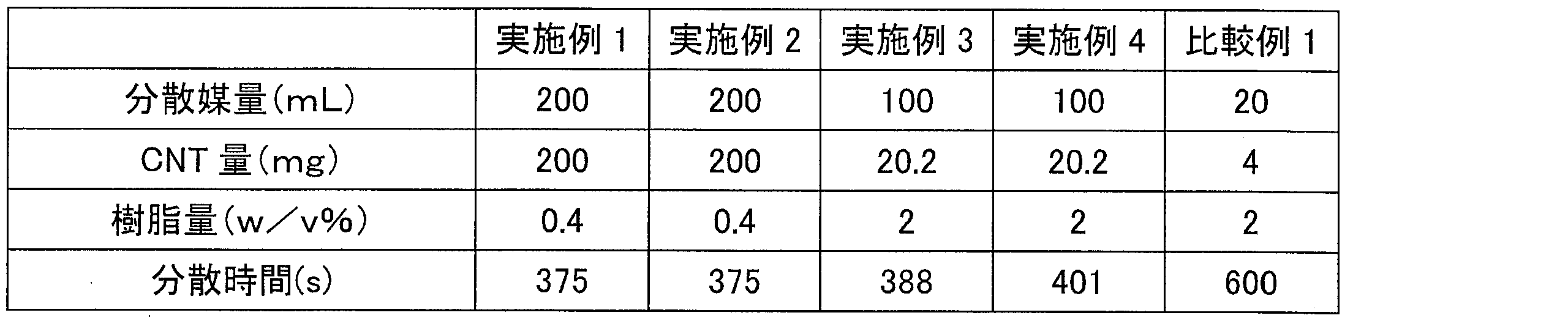

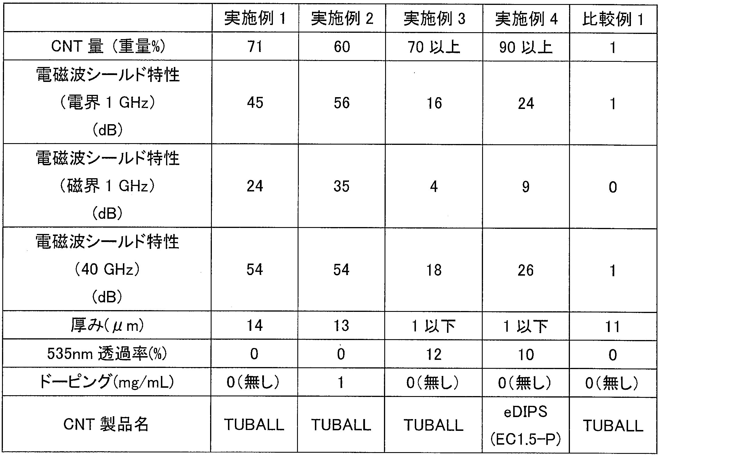
表3より、カーボンナノチューブの含有量が60重量%以上である実施例1~4は、比較例1と比較して、1GHzの電界波、1GHzの磁界波、40GHzの電磁波のいずれに対しても高い遮蔽効果を示していることが分かる。
また、実施例3および4は、厚みが1μm以下であるため、波長535nmの光に対して透過性を有することも分かる。
本発明は、電磁波シールド材料として好適に利用することができる。
11a 電界波シールド特性測定装置
11b 磁界波シールド特性測定装置
13 測定治具
14 中心導体
15 測定治具
16 ループアンテナ
21 スペクトラムアナライザ
22 アッテネータ
23 アッテネータ
24 プリアンプ
31 同軸導波管アダプタ
32 導波管サンプルホルダ
41 ネットワークアナライザ
101 測定試料
11b 磁界波シールド特性測定装置
13 測定治具
14 中心導体
15 測定治具
16 ループアンテナ
21 スペクトラムアナライザ
22 アッテネータ
23 アッテネータ
24 プリアンプ
31 同軸導波管アダプタ
32 導波管サンプルホルダ
41 ネットワークアナライザ
101 測定試料
Claims (9)
- 樹脂およびカーボンナノチューブを含み、当該カーボンナノチューブを60重量%以上含む、電磁波シールド材料。
- シート状である、請求項1に記載の電磁波シールド材料。
- 厚みが100nm以上、100μm以下である、請求項2に記載の電磁波シールド材料。
- 535nmの波長の光の透過率が10%以上である、請求項3に記載の電磁波シールド材料。
- 上記樹脂はセルロース誘導体を含む、請求項1~4のいずれか1項に記載の電磁波シールド材料。
- ドーパントをさらに含むことを特徴とする、請求項1~5のいずれか1項に記載の電磁波シールド材料。
- 樹脂およびカーボンナノチューブを含む組成物を加熱することにより樹脂を灰化させる工程を含む、電磁波シールド材料の製造方法。
- 上記樹脂はセルロース誘導体を含む、請求項7に記載の電磁波シールド材料の製造方法。
- 上記組成物はドーパントをさらに含む、請求項7または8に記載の電磁波シールド材料の製造方法。
Priority Applications (3)
| Application Number | Priority Date | Filing Date | Title |
|---|---|---|---|
| CN202080099342.7A CN115399085A (zh) | 2020-03-30 | 2020-11-06 | 电磁波屏蔽材料及其制造方法 |
| KR1020227028336A KR20220161266A (ko) | 2020-03-30 | 2020-11-06 | 전자파 차폐 재료 및 그 제조 방법 |
| JP2022511508A JPWO2021199477A1 (ja) | 2020-03-30 | 2020-11-06 |
Applications Claiming Priority (2)
| Application Number | Priority Date | Filing Date | Title |
|---|---|---|---|
| JP2020-060977 | 2020-03-30 | ||
| JP2020060977 | 2020-03-30 |
Publications (1)
| Publication Number | Publication Date |
|---|---|
| WO2021199477A1 true WO2021199477A1 (ja) | 2021-10-07 |
Family
ID=77928039
Family Applications (1)
| Application Number | Title | Priority Date | Filing Date |
|---|---|---|---|
| PCT/JP2020/041450 Ceased WO2021199477A1 (ja) | 2020-03-30 | 2020-11-06 | 電磁波シールド材料およびその製造方法 |
Country Status (4)
| Country | Link |
|---|---|
| JP (1) | JPWO2021199477A1 (ja) |
| KR (1) | KR20220161266A (ja) |
| CN (1) | CN115399085A (ja) |
| WO (1) | WO2021199477A1 (ja) |
Citations (1)
| Publication number | Priority date | Publication date | Assignee | Title |
|---|---|---|---|---|
| JP2011014650A (ja) * | 2009-06-30 | 2011-01-20 | Panasonic Electric Works Co Ltd | 電磁シールド性成形材料、電子部品用電磁シールド性成形品、建材用電磁シールド性成形品、及び電磁シールド性成形材料の製造方法 |
Family Cites Families (5)
| Publication number | Priority date | Publication date | Assignee | Title |
|---|---|---|---|---|
| JP2002290094A (ja) * | 2001-03-27 | 2002-10-04 | Toray Ind Inc | 電磁波シールド性材料およびその成形体 |
| JP6246089B2 (ja) * | 2014-07-17 | 2017-12-13 | 富士フイルム株式会社 | 導電性フィルム、タッチパネル付き表示装置 |
| JP6278922B2 (ja) * | 2015-03-30 | 2018-02-14 | Jx金属株式会社 | 電磁波シールド材 |
| JP6613319B2 (ja) | 2015-12-25 | 2019-11-27 | 国立研究開発法人産業技術総合研究所 | 電磁波遮蔽カーボンナノチューブ高分子複合材料、電磁波遮蔽材料、及び電磁波遮蔽カーボンナノチューブ高分子複合材料の製造方法 |
| WO2018066574A1 (ja) * | 2016-10-04 | 2018-04-12 | 日本ゼオン株式会社 | 電磁波シールド構造体およびその製造方法 |
-
2020
- 2020-11-06 JP JP2022511508A patent/JPWO2021199477A1/ja active Pending
- 2020-11-06 WO PCT/JP2020/041450 patent/WO2021199477A1/ja not_active Ceased
- 2020-11-06 CN CN202080099342.7A patent/CN115399085A/zh not_active Withdrawn
- 2020-11-06 KR KR1020227028336A patent/KR20220161266A/ko not_active Withdrawn
Patent Citations (1)
| Publication number | Priority date | Publication date | Assignee | Title |
|---|---|---|---|---|
| JP2011014650A (ja) * | 2009-06-30 | 2011-01-20 | Panasonic Electric Works Co Ltd | 電磁シールド性成形材料、電子部品用電磁シールド性成形品、建材用電磁シールド性成形品、及び電磁シールド性成形材料の製造方法 |
Also Published As
| Publication number | Publication date |
|---|---|
| CN115399085A (zh) | 2022-11-25 |
| JPWO2021199477A1 (ja) | 2021-10-07 |
| KR20220161266A (ko) | 2022-12-06 |
Similar Documents
| Publication | Publication Date | Title |
|---|---|---|
| JP7120973B2 (ja) | 融着ネットワークを有する透明導電性フィルムの形成のための金属ナノワイヤーインク | |
| JP6274309B2 (ja) | カーボンナノチューブ分散液および導電性フィルムの製造方法 | |
| EP2547735B1 (en) | Anti-corrosion agents for transparent conductive film | |
| Huang et al. | Experimental demonstration of printed graphene nano-flakes enabled flexible and conformable wideband radar absorbers | |
| US11104813B2 (en) | Dispersion | |
| JP2022068877A (ja) | 金属ナノワイヤおよびポリマーバインダーを主成分とする透明導電性コーティング、その溶液処理、およびパターン化方法 | |
| JP5596609B2 (ja) | 金属コロイド溶液及びそれを用いた塗料 | |
| KR102023374B1 (ko) | 인쇄용 구리 페이스트 조성물 및 이를 이용한 금속패턴의 형성방법 | |
| EP2154108A1 (en) | Single-walled carbon nanotube dispersion liquid and method for producing single-walled carbon nanotube dispersion liquid | |
| JP6859083B2 (ja) | 導電性フィルム、及び導電性フィルムの製造方法 | |
| KR20150134728A (ko) | 전도성 조성물 | |
| CN104010752A (zh) | 银微粒及其制造方法、以及含有该银微粒的导电性糊、导电性膜和电子器件 | |
| EP2738776A1 (en) | Transparent conductor and method for producing same | |
| EP0182744A2 (de) | Photohärtbare gefüllte Expoxidharz-Zusammensetzungen und deren Verwendung | |
| WO2014061556A1 (ja) | 導電性基板用金属粒子分散体及びその製造方法、並びに導電性基板の製造方法 | |
| WO2021199477A1 (ja) | 電磁波シールド材料およびその製造方法 | |
| JP6080233B2 (ja) | 機能性光透過材およびその製造方法 | |
| JP2009512970A (ja) | 導電線パターン形成のための銀オルガノゾルインク | |
| JP2014196427A (ja) | 導電膜形成用組成物およびこれを用いる導電膜の製造方法 | |
| WO2019026829A1 (ja) | 導電フィルムの製造方法、導電フィルム及び金属ナノワイヤインク | |
| WO2013175965A1 (ja) | 導電性組成物及びそれにより導電膜が形成された回路基板 | |
| KR101232835B1 (ko) | 전도성 박막 형성 방법 | |
| JP5151229B2 (ja) | 太陽電池の電極形成用組成物及び該電極の形成方法並びに該形成方法により得られた電極を用いた太陽電池の製造方法 | |
| CN114216949B (zh) | 一种丝网印刷电极、及其制作方法和检测方法 | |
| JP2002338850A (ja) | 金属コロイド溶液及びその製造方法並びに金属コロイド溶液から得られる皮膜 |
Legal Events
| Date | Code | Title | Description |
|---|---|---|---|
| 121 | Ep: the epo has been informed by wipo that ep was designated in this application |
Ref document number: 20929557 Country of ref document: EP Kind code of ref document: A1 |
|
| ENP | Entry into the national phase |
Ref document number: 2022511508 Country of ref document: JP Kind code of ref document: A |
|
| NENP | Non-entry into the national phase |
Ref country code: DE |
|
| 122 | Ep: pct application non-entry in european phase |
Ref document number: 20929557 Country of ref document: EP Kind code of ref document: A1 |