WO2021192042A1 - ノイズ低減装置 - Google Patents
ノイズ低減装置 Download PDFInfo
- Publication number
- WO2021192042A1 WO2021192042A1 PCT/JP2020/013042 JP2020013042W WO2021192042A1 WO 2021192042 A1 WO2021192042 A1 WO 2021192042A1 JP 2020013042 W JP2020013042 W JP 2020013042W WO 2021192042 A1 WO2021192042 A1 WO 2021192042A1
- Authority
- WO
- WIPO (PCT)
- Prior art keywords
- compensation signal
- noise
- frequency component
- unit
- phase
- Prior art date
- Legal status (The legal status is an assumption and is not a legal conclusion. Google has not performed a legal analysis and makes no representation as to the accuracy of the status listed.)
- Ceased
Links
Images




Classifications
-
- H—ELECTRICITY
- H03—ELECTRONIC CIRCUITRY
- H03K—PULSE TECHNIQUE
- H03K5/00—Manipulating of pulses not covered by one of the other main groups of this subclass
- H03K5/125—Discriminating pulses
- H03K5/1252—Suppression or limitation of noise or interference
-
- G—PHYSICS
- G05—CONTROLLING; REGULATING
- G05F—SYSTEMS FOR REGULATING ELECTRIC OR MAGNETIC VARIABLES
- G05F1/00—Automatic systems in which deviations of an electric quantity from one or more predetermined values are detected at the output of the system and fed back to a device within the system to restore the detected quantity to its predetermined value or values, i.e. retroactive systems
- G05F1/10—Regulating voltage or current
-
- H—ELECTRICITY
- H02—GENERATION; CONVERSION OR DISTRIBUTION OF ELECTRIC POWER
- H02J—ELECTRIC POWER NETWORKS; CIRCUIT ARRANGEMENTS OR SYSTEMS FOR SUPPLYING OR DISTRIBUTING ELECTRIC POWER; SYSTEMS FOR STORING ELECTRIC ENERGY
- H02J1/00—Circuit arrangements for DC mains or DC distribution networks
- H02J1/02—Arrangements for reducing harmonics or ripples
-
- H—ELECTRICITY
- H02—GENERATION; CONVERSION OR DISTRIBUTION OF ELECTRIC POWER
- H02M—APPARATUS FOR CONVERSION BETWEEN AC AND AC, BETWEEN AC AND DC, OR BETWEEN DC AND DC, AND FOR USE WITH MAINS OR SIMILAR POWER SUPPLY SYSTEMS; CONVERSION OF DC OR AC INPUT POWER INTO SURGE OUTPUT POWER; CONTROL OR REGULATION THEREOF
- H02M1/00—Details of apparatus for conversion
- H02M1/12—Arrangements for reducing harmonics from AC input or output
-
- H—ELECTRICITY
- H02—GENERATION; CONVERSION OR DISTRIBUTION OF ELECTRIC POWER
- H02M—APPARATUS FOR CONVERSION BETWEEN AC AND AC, BETWEEN AC AND DC, OR BETWEEN DC AND DC, AND FOR USE WITH MAINS OR SIMILAR POWER SUPPLY SYSTEMS; CONVERSION OF DC OR AC INPUT POWER INTO SURGE OUTPUT POWER; CONTROL OR REGULATION THEREOF
- H02M7/00—Conversion of AC power input into DC power output; Conversion of DC power input into AC power output
- H02M7/42—Conversion of DC power input into AC power output without possibility of reversal
- H02M7/44—Conversion of DC power input into AC power output without possibility of reversal by static converters
- H02M7/48—Conversion of DC power input into AC power output without possibility of reversal by static converters using discharge tubes with control electrode or semiconductor devices with control electrode
-
- H—ELECTRICITY
- H03—ELECTRONIC CIRCUITRY
- H03K—PULSE TECHNIQUE
- H03K5/00—Manipulating of pulses not covered by one of the other main groups of this subclass
- H03K2005/00286—Phase shifter, i.e. the delay between the output and input pulse is dependent on the frequency, and such that a phase difference is obtained independent of the frequency
Definitions
- This disclosure relates to a noise reduction device.
- noise electromagnetic noise generated from power electronics equipment
- a noise reduction device such as a transistor and an operational amplifier
- the basic configuration of an active filter is usually a function of detecting noise to be reduced existing in the main circuit, a function of generating a compensation voltage or a compensation current for reducing the detected noise by an active element, and a function of generating a compensation current or a compensation current by the active element.
- the ability to inject the generated compensating voltage or compensating current into the main circuit is required.
- an active filter for reducing the common mode current an active filter including a buffer amplifier in which the output of a current transformer that monitors the common mode current is input is used. , A configuration for generating a compensating current is disclosed.
- Patent Document 1 does not mention a method of suppressing a signal that amplifies noise due to a phase delay generated in a compensation current. Further, as described in Patent Document 1, there are a feedback control method and a feedforward control method as control methods related to noise reduction of an active filter.
- the noise amplification signal caused by the phase delay only amplifies the noise existing in the main circuit as it is.
- the noise amplification signal caused by the phase delay brings about positive feedback of noise and oscillates the active filter to destabilize the operation. Therefore, in the feedback control method, it is particularly desired to suppress the noise amplification signal due to the phase lag.
- the feedback control type active filter it is required to increase the gain of the feedback loop in order to enhance the noise reduction effect, but the increase of the gain may also increase the noise amplification signal due to the phase lag. There is. Therefore, in the feedback control type active filter, it tends to be difficult to obtain a high noise reduction effect while suppressing oscillation.
- the present disclosure has focused on the above problems, and an object of the present disclosure is to provide a feedback control type noise reduction device having high stability and a high noise reduction effect.
- the noise reduction device includes a noise detection unit, a compensation signal generation unit, a compensation signal injection unit, a compensation signal detection unit, a low frequency component subtraction unit, and an intermediate frequency component addition unit.
- the noise detection unit detects electromagnetic noise on the connecting line.
- the compensation signal generation unit generates a compensation signal for canceling electromagnetic noise based on the detection signal of the noise detection unit.
- the compensation signal injection unit injects the compensation signal into the connecting line.
- the compensation signal detection unit detects the compensation signal.
- the low frequency component subtraction unit amplifies the first frequency component of the first frequency region lower than the predetermined first frequency among the detection signals by the compensation signal detection unit, and negatively affects the compensation signal generation unit.
- the intermediate frequency component addition unit positively feeds back the component of the predetermined second frequency higher than the first frequency of the detection signals by the compensation signal detection unit to the compensation signal generation unit.
- the noise reduction effect of the second frequency is enhanced, and the effect of reducing the noise of the second frequency is enhanced.
- a feedback control type noise reduction device with high stability can be realized.
- FIG. 2 It is a control block diagram of the noise reduction apparatus which concerns on Embodiment 1.
- FIG. 2 is a control block diagram of the noise reduction apparatus which concerns on Embodiment 2.
- FIG. 2 is an electric circuit diagram for realizing the control block diagram of FIG. 2 by hardware. It is an electric circuit diagram for evaluating the one-circle transfer function of the major feedback loop of the noise reduction apparatus shown in FIG. It is an electric circuit diagram for evaluating the one-circle transfer function of the minor feedback loop of the noise reduction apparatus shown in FIG. It is a graph which shows the analysis result of the one-circle transfer function of the major feedback loop of the noise reduction apparatus which concerns on Embodiment 2.
- FIG. 2 It is a graph which shows the analysis result of the one-circle transfer function of the minor feedback loop of the noise reduction apparatus which concerns on Embodiment 2.
- FIG. It is a graph which shows the analysis result of the one-circle transfer function of the minor feedback loop of the noise reduction apparatus which concerns on Embodiment 3.
- FIG. It is a graph which shows the analysis result of the one-circle transfer function of the major feedback loop of the noise reduction apparatus which concerns on Embodiment 3.
- FIG. It is a graph which shows the analysis result of the one-circle transfer function of the minor feedback loop of the noise reduction apparatus which concerns on Embodiment 4.
- FIG. It is a graph which shows the analysis result of the one-circle transfer function of the major feedback loop of the noise reduction apparatus which concerns on Embodiment 4.
- FIG. It is a graph which shows the actual measurement result of the noise reduction effect by the noise reduction apparatus which concerns on Embodiment 4. This is an example of an actually measured waveform of a compensation signal in the noise reduction device according to
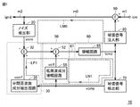
- FIG. 1 is a control block diagram of the noise reduction device according to the first embodiment.
- the noise reduction device 10 includes a noise detection unit 20, an intermediate frequency component addition unit 30, a low frequency component subtraction unit 50, a compensation signal generation unit 60, and a compensation signal detection unit 70.
- a compensation signal injection unit 80 and a connection line m0 are provided.
- connection line m0 is connected to the noise source current input line m1 for inputting the noise source current icm via the subtractor type operator 90.
- the compensation signal injection unit 80 is connected to the connection line m0 via a subtractor type operator 90.
- the noise detection unit 20 is connected to the connection line m0 in a manner of sandwiching the connection line m0 together with the subtractor type operator 90. As will be described later, the noise detection unit 20 can be configured by a current transformer or a capacitor. Further, the noise detection unit 20 is connected to the leakage noise current output line m2 that outputs the leakage noise current ignd on the opposite side of the connection side from the connection line m0. The noise detection unit 20 outputs a detection voltage vsns that changes according to the current of the connection line m0. Therefore, the detected voltage vsns contains an electromagnetic noise component.
- the intermediate frequency component addition unit 30 includes an adder type operator 32 and an intermediate frequency component extraction circuit 35.
- the intermediate frequency component addition unit 30 is connected to the input line 61 of the compensation signal generation unit via a subtractor type operator 52 in the low frequency component subtraction unit 50.
- the low frequency component subtraction unit 50 includes a subtractor type operator 52 and a low frequency component amplifier circuit 55.
- the low-frequency component amplifier circuit 55 is connected to the input line 61 of the compensation signal generation unit via a subtractor type operator 52.
- the compensation signal generation unit 60 includes an amplifier circuit 65.
- the amplifier circuit 65 amplifies the voltage of the input line 61 to generate a compensation signal ICMP corresponding to the compensation current.
- the compensation signal detection unit 70 outputs a compensation signal detection voltage vcmp according to the compensation signal icmp.
- the intermediate frequency component addition unit 30 generates an output signal vcmf obtained by extracting a predetermined intermediate frequency component from the compensation signal detection voltage vcmp.
- the low-frequency component amplifier circuit 55 generates an output signal vclf from which a low-frequency component having a compensation signal detection voltage vcmp is extracted.
- the noise reduction device 10 forms a feedback loop LM0 via a connection line m0, a noise detection unit 20, a compensation signal generation unit 60, a compensation signal injection unit 80, and a subtractor type operator 90.
- this feedback loop is defined as a “major feedback loop”.
- the compensation signal icmp injected by the subtractor type operator 90 is generated so as to cancel the electromagnetic noise component.
- electromagnetic noise remains on the connection line m0 as a residual deviation depending on the magnitude of the gain of the major feedback loop.
- the compensation signal detection voltage vcmp from the compensation signal detection unit 70 is input to the low frequency component amplifier circuit 55.
- the low frequency component subtraction unit 50 forms a feedback loop LN1 via the low frequency component amplifier circuit 55, the subtractor type operator 52, the compensation signal generation unit 60, and the compensation signal detection unit 70.
- negative feedback is formed by the subtractor type operator 52, so the feedback loop is defined below as a "negative minor feedback loop”.
- the negative minor feedback loop LN1 feedback control is performed so that the low frequency component in the compensation signal ICMP corresponding to the one-round transfer function (frequency characteristic) of the negative minor feedback loop is set to 0 by forming the negative feedback. It is said.
- the low frequency component in the compensation signal icmp causes unnecessary power consumption or narrows the amplitude of the voltage and current output in the compensation signal generation unit 60. Furthermore, there is a concern that forming positive feedback in the major feedback loop may cause closed-loop oscillation.
- the compensation signal detection voltage vcmp from the compensation signal detection unit 70 is input to the intermediate frequency component extraction circuit 35.
- the intermediate frequency component addition unit 30 forms the feedback loop LP1 via the intermediate frequency component extraction circuit 35, the adder type operator 32, the compensation signal generation unit 60, and the compensation signal detection unit 70.
- the feedback loop LP1 positive feedback is formed by the adder type operator 32. Therefore, the feedback loop is defined below as a “positive minor feedback loop”.
- feedback control is performed so as to amplify the intermediate frequency component in the compensation signal imp according to the one-round transfer function (frequency characteristic) of the positive minor feedback loop by forming the positive feedback. It is said.
- the intermediate frequency can be variably set by adjusting the one-round transfer function (frequency characteristic) of the positive minor feedback loop LP1. Therefore, by adjusting the circular transfer function of the positive minor feedback loop LP1 so that the intermediate frequency is set to an arbitrary frequency to be noise-reduced, the noise reduction device 10 has a high noise reduction effect at an arbitrary frequency. Can be demonstrated.
- the gain of the positive minor feedback loop LP1 generally needs to be less than 1.
- the positive minor feedback loop LP1 causes closed-loop oscillation, so that a signal equal to or larger than the input limit value is input to the compensation signal generation unit 60 or the like, and a desired noise reduction operation is performed. This is because there is a risk that
- the major feedback loop LM0 under the action of the positive minor feedback loop LP1 and the negative minor feedback loop LN1, the major feedback loop LM0 generates a compensation signal imp that acts as a noise canceling component.
- the compensation signal icmp the component of the frequency (intermediate frequency) to be reduced by the noise is amplified by the positive minor feedback loop LP1, and the low frequency component is reduced by the negative minor feedback loop LN1. It will be generated.
- the low frequency component (including the offset component) of the compensation signal impp is suppressed to reduce the power consumption and stabilize the operation, and then the intermediate frequency component is used. A high noise reduction effect due to amplification can be obtained.
- FIG. 2 is a control block diagram of the noise reduction device 10x according to the second embodiment.
- the noise reduction device 10x according to the second embodiment corresponds to a device in which the control block of the noise reduction device 10 shown in FIG. 1 is modified into a configuration suitable for mounting.
- the noise reduction device 10x according to the second embodiment is different from the noise reduction device 10 shown in FIG. 1 in the following points.
- the compensation signal generation unit 60 further has a reverse phase conversion element 66 in addition to the amplifier circuit 65. Therefore, in FIG. 2, the phase of the compensation signal icmp output from the compensation signal generation unit 60 is inverted from that of the compensation signal icmp in FIG.
- An adder type operator 90x is arranged on the connection line m0 instead of the subtractor type operator 90 in FIG. Therefore, the compensation signal icmp from the compensation signal generation unit 60 is injected into the connection line m0 via the adder type operator 90x.
- the intermediate frequency component addition unit 30 further includes a phase inversion element 33 and a reverse phase conversion element 34 in addition to the intermediate frequency component extraction circuit 35. Further, instead of the adder type operator 32, the subtractor type operator 32x is arranged. The output signal vcmf of the intermediate frequency component extraction circuit 35 is input to the ⁇ side of the operator 32x after the antiphase conversion and the phase inversion.
- the low frequency component subtraction unit 50 further includes a reverse phase conversion element 53 in addition to the subtractor type operator 52 and the low frequency component amplifier circuit 55.
- the output signal vclf of the low-frequency component amplifier circuit 55 is input to the ⁇ side of the operator 52 after the reverse phase conversion.
- the reverse phase conversion elements 34, 53, 66 can be configured by using, for example, an inverting amplifier circuit composed of an operational amplifier or a transistor. Further, the phase inversion element 33 can be configured by utilizing the phase inversion that occurs as a result of adjusting the phase lag at a high frequency of the operational amplifier or the transistor.
- the phase of the compensation signal icmp from the compensation signal generation unit 60 is inverted as compared with the control configuration of FIG.
- the compensation signal ICMP is injected into the connection line m0 via the adder type operator 90x instead of the subtractor type operator 90 in FIG. Therefore, it is understood that the compensation signal ICMP injected into the connection line m0 has the same phase between FIGS. 1 and 2.
- the phase of the compensation signal detection voltage vcmp from the compensation signal detection unit 70 is also inverted from that of FIG.
- the output signal vclf of the low frequency component amplifier circuit 55 is input to the subtractor type operator 52 (-side) after the reverse phase conversion. Therefore, it is understood that the sign (positive / negative) of the compensation signal detection voltage vcmp acting on the calculation by the operator 52 is the same in FIGS. 1 and 2.
- the output signal vcmf generated by the intermediate frequency component extraction circuit 35 from the compensation signal detection voltage vcmp whose phase is inverted from FIG. 1 is further phase inverted after reverse phase conversion, and is a subtractor type. It is input to the operator 32x (-side) of. Therefore, the sign (positive / negative) of the compensation signal detection voltage vcmp acting on the calculation is the same between the operator 32 (adder type) in FIG. 1 and the operator 32x (subtractor type) in FIG. Is understood to be.
- the symbols of the signal vcmf and the output signal vclf related to the low frequency are the same. Therefore, it is understood that the noise reduction device 10x of FIG. 2 and the noise reduction device 10 of FIG. 1 realize the same control contents.
- the operator 52 in the low frequency component subtraction unit 50 and the operator 32x in the intermediate frequency component addition unit 30 can both be configured by the subtractor type, so that they are hardware. It is possible to combine them into a common circuit at the time of mounting.
- the adder type operator 90x to the connection line m0, the options of the hardware constituting the compensation signal injection unit 80 are increased.
- FIG. 3 is an electric circuit diagram for realizing the control block diagram of the noise reduction device 10x shown in FIG. 2 by hardware.
- the noise reduction device 10x includes a connection line m0, a noise detection unit 20, a compensation signal generation unit 60, a compensation signal injection unit 80, a compensation signal detection unit 70, and an intermediate frequency.
- a dual-purpose circuit 100 having the functions of the component addition unit 30 and the low frequency component subtraction unit 50 is provided.
- the noise source circuit 11 that generates the noise source current icm shown in FIG. 1 is connected to the noise source current input line m1.
- the noise source circuit 11 is, for example, an inverter circuit, and generates a noise source current by switching semiconductor elements for power conversion.
- a noise leakage circuit 12 is connected to the leakage noise current output line m2.
- the noise leakage circuit 12 is a general term for a group of circuits that may malfunction due to the inflow of noise, and is, for example, an IC (Integrated Circuit), a system power supply that constitutes a power supply path to the IC, or the like.
- the voltage of the system power supply is AC / DC converted by a rectifying circuit, and then DC / AC conversion is performed from an inverter circuit to a motor or the like.
- the inverter circuit of the one electric device becomes the noise source circuit 11, and the noise generated by the inverter circuit passes through the rectifier circuit and the system power supply and is a component of the other electric device.
- the leakage circuit 12 for example, IC or the like.
- connection line m0 the noise source current input line m1
- leakage noise current output line m2 the leakage noise current output line m2
- the noise detection unit 20 is composed of a current transformer 21.
- the current transformer 21 has primary windings 21y and 21z inserted in the connection line m0 and secondary windings 21x.
- the primary windings 21y and 21z and the secondary winding 21x are magnetically coupled, and the voltage that changes according to the current flowing through the connection line m0 is the secondary winding as the detection voltage vsns shown in FIG. Occurs at 21x.
- the detected voltage vsns includes a voltage component that reflects an electromagnetic noise component in the current of the connection line m0.
- the compensation signal injection unit 80 is composed of a current transformer having a primary winding 81x and secondary windings 81y and 81z that are magnetically coupled to each other.
- the secondary windings 81y and 81z are inserted in the connecting line m0.
- the compensation signal icmp which is the output current of the compensation signal generation unit 60, flows through the primary winding 81x.
- the noise detection unit 20 can be configured by a capacitor as is known. Further, the signal injection unit 80 can also be applied with a capacitor by adopting the control configuration of FIG. 2 using the adder type operator 90x.
- the compensation signal generation unit 60 includes a differential inverting amplifier circuit 150 and an emitter follower 180.
- the differential inverting amplifier circuit 150 includes an operational amplifier 170 and a phase adjusting circuit 160 of the operational amplifier 170.
- the phase adjusting circuit 160 has a negative input resistor 161 and a feedback resistor 163, and a feedback capacitance 164. Further, a positive input resistor 162 is connected to the input terminal (+ side) of the operational amplifier 170.
- the phase adjustment circuit 160 is connected between the input terminal (-side) of the operational amplifier 170 and the output terminal.
- the phase adjustment circuit 160 can adjust the phase difference between the input and output of the differential inverting amplifier circuit 150.
- a low-pass filter is composed of a negative input resistor 161, a feedback resistor 163, and a feedback capacitance 164.
- the emitter follower 180 has transistors 181 and 182 having control electrodes connected to the output terminal of the operational amplifier 170. Transistors 181 and 182 are connected in series between a positive power supply node (V +) and a negative power supply node (V ⁇ ). Compensation signal icmp, which is the output of the compensation signal generation unit 60, is generated at the connection node of the transistors 181 and 182. By connecting the primary winding 81x of the current transformer 81 between the connection nodes of the transistors 181 and 182 and the ground (GND), as shown in FIG. 2, the connection line is passed through the signal injection unit 80. The compensation signal icmp can be injected into m0.
- the arrangement of the emitter follower 180 can be omitted.
- the differential inverting amplifier circuit 150 can be configured by using transistors without using operational amplifiers.
- a detection resistor 71 constituting the compensation signal detection unit 70 is connected between the primary winding 81x of the current transformer 81 and the ground (GND). As a result, a compensation signal detection voltage vcmp proportional to the current value of the compensation signal icmp is generated in the detection resistor 71.
- the dual-purpose circuit 100 having the functions of the intermediate frequency component addition unit 30 and the low frequency component subtraction unit 50 is composed of an inverting amplifier circuit 110.
- the inverting amplifier circuit 110 includes an operational amplifier 115 and a phase adjusting circuit 120 of the operational amplifier 115.
- the phase adjusting circuit 120 has a negative input resistor 121, a feedback resistor 122, and a feedback capacitance 123.
- the phase adjustment circuit 120 can adjust the phase difference between the input and output of the inverting amplifier circuit 110.
- a low-pass filter is composed of a negative input resistor 121, a feedback resistor 122, and a feedback capacitance 123.
- a negative input resistor 121 and a detection resistor 71 are input between the input terminals of the operational amplifier 115.
- the input voltage of the operational amplifier 115 is set to the compensation signal detection voltage vcmp, and as shown in FIG. 2, the compensation signal detection voltage vcmp is the intermediate frequency component addition unit 30 and the low frequency component subtraction unit 50. Will be entered in.
- the output terminal of the inverting amplifier circuit 110 is connected to the input terminal (+ side) of the operational amplifier 170 of the compensation signal generation unit 60. Therefore, the differential inverting amplifier circuit 150 amplifies the voltage difference between the detection voltage vsns from the noise detection unit 20 and the output signal of the inverting amplifier circuit 110 to generate a compensation signal icmp. This constitutes a minor loop of the compensation signal icmp.
- the inverting amplifier circuit 110 can also be configured by using a transistor without using an operational amplifier.
- the operational amplifiers 115 and 170 and the transistors 181, 182 operate by receiving the supply of the power supply voltage V + (positive voltage) and V- (negative voltage).
- the power supply voltages V + and V- can be supplied by a positive direct current power supply PS + and a negative direct current power supply PS- connected in series via ground (GND).
- Each of the DC power supplies PS + and PS- can be configured by a DC stabilized power supply that outputs a positive voltage.
- a DC power supply can be obtained by rectifying the AC current flowing through the noise leakage circuit 12 and supplying it to a switching power supply circuit (not shown).
- both functions of the antiphase conversion elements 34 and 53 in FIG. 2 are realized.
- the function of the reverse phase conversion element 66 in FIG. 2 is realized by the inverting amplification of the differential inverting amplifier circuit 150.
- the function of the phase inversion element 33 in FIG. 2 is realized by adjusting the phase delay of the inverting amplifier circuit 110 by adjusting the circuit constant of the phase adjustment circuit 120. Specifically, it can be realized by adding a phase delay of ⁇ 180 ° to the frequency component corresponding to the intermediate frequency.
- the noise reduction device 10x forms a major feedback loop LM0 via the connection line m0, the noise detection unit 20, the compensation signal generation unit 60, and the compensation signal injection unit 80.
- the major feedback loop LM0 since the differential inverting amplifier circuit 150 forms negative feedback, feedback control is executed so as to eliminate the electromagnetic noise existing in the connection line m0.
- electromagnetic noise remains on the connection line m0 as a residual deviation according to the magnitude of the gain of the major feedback loop LM0.
- the gain of the major feedback loop LM0 is determined by setting the turns ratio between the primary windings 21y and 21z and the secondary winding 21x in the noise detection unit 20 or adjusting the gain of the differential inverting amplifier circuit 150 in the compensation signal generation unit 60. , Can be made larger.
- a minor feedback loop is formed via an inverting amplifier circuit 110 that integrally constitutes an intermediate frequency component addition unit 30 and a low frequency component subtraction unit 50, a compensation signal generation unit 60, and a compensation signal detection unit 70.
- the minor feedback loop forms negative feedback
- feedback control is performed so that the low frequency component in the compensation signal ICMP corresponding to the one-round transfer function (frequency characteristic) of the minor feedback loop is set to zero.
- the minor feedback loop forms positive feedback by generating a signal whose phase is inverted at a certain frequency or higher according to the circular transfer function (frequency characteristic) of the minor feedback loop.
- feedback control can be performed so as to amplify the intermediate frequency component in the compensation signal imp according to the one-round transfer function (frequency characteristic) of the minor feedback loop.
- the frequency regions of the one-round transmission function (frequency characteristics) of the minor feedback loop are different from each other. It is possible to equivalently form the positive minor feedback loop LP1 for the intermediate frequency and the negative minor feedback loop LN1 for the low frequency component in FIGS. 1 and 2.
- the round transfer function (frequency characteristics) of the minor feedback loop should be adjusted so that the frequency domain (intermediate frequency) in which the equivalently positive minor feedback loop is formed corresponds to an arbitrary frequency to be noise-reduced. Therefore, a high noise reduction effect can be exhibited at any frequency.
- the gain of the positive minor feedback loop needs to be less than 1. This is because when the gain is 1 or more, closed-loop oscillation occurs in the positive feedback.
- the one-round transfer function (frequency characteristic) of the minor feedback loop can be adjusted so that a negative minor feedback loop is formed equivalently. This can bring about the effects of suppressing unnecessary power consumption in the major feedback loop LM0, securing the amplitudes of the voltage and current outputs, and stabilizing the operation by suppressing the closed loop oscillation.
- the circular transmission function (frequency characteristic) of the minor feedback loop, the gain of the positive minor feedback loop, and the intermediate frequency in FIG. 3 are the compensation signal generation unit 60, the compensation signal detection unit 70, and the intermediate frequency component addition unit 30. And, by adjusting the circuit constant in the low frequency component subtraction unit 50 (inverting amplifier circuit 110), it can be changed to an arbitrary characteristic.
- FIG. 4 is an electric circuit diagram for evaluating the one-round transfer function of the major feedback loop of the noise reduction device 10x shown in FIG.
- the wiring between the noise detection unit 20 and the negative input resistor 161 in the compensation signal generation unit 60 is opened to input a voltage.
- a terminal 201 and a voltage measurement terminal 202 are provided.
- a circuit transfer function of a major feedback loop was obtained by circuit simulation using such a circuit as an analysis target.
- the voltage input terminal 201 is provided on the negative input resistor 161 side
- the voltage measurement terminal 202 is provided on the noise detection unit 20 side.
- the minor feedback loop by the inverting amplifier circuit 110 was set as a closed loop.
- a voltage corresponding to the current of the connection line m0 into which the compensation signal imp is injected which is provided with the minor feedback loop by the inverting amplifier circuit 110 and is generated by the compensation signal generation unit 60, is generated.
- the main circuit was in a non-powered state.
- the major feedback loop to be analyzed in FIG. 4 corresponds to an embodiment of the “first feedback loop”.
- FIG. 5 is an electric circuit diagram for evaluating the one-round transfer function of the minor feedback loop of the noise reduction device 10x shown in FIG.
- the wiring between the noise detection unit 20 and the negative input resistor 161 in the compensation signal generation unit 60 is opened as in FIG. A point 300 is provided. Further, a circuit provided with a voltage input terminal 301 and a voltage measurement terminal 302 by opening the wiring between the compensation signal injection unit 80 (primary winding 81x) and the output node of the compensation signal generation unit 60 is simulated. Was the subject of analysis.
- the compensation signal injection unit 80 (primary winding 81x) is provided with a voltage input terminal 301, and the compensation signal generation unit 60 side is provided with a voltage measurement terminal 302.
- both the major feedback loop and the minor feedback loop are open loops.
- the main circuit was also in a non-powered state.
- the minor feedback loop analyzed in FIG. 5 corresponds to an embodiment of the “second feedback loop”.
- FIG. 6 is a graph showing the analysis result of the one-round transfer function of the major feedback loop of the noise reduction device according to the second embodiment.
- FIG. 6A shows the analysis result only for the major feedback loop by the compensation signal generation unit 60 in which the intermediate frequency component addition unit 30 and the low frequency component subtraction unit 50 are removed in the control block diagram of FIG.
- This analysis target corresponds to a configuration in which the inverting amplifier circuit 110 is removed from the configuration of FIG.
- the characteristic line G-AFa shows the gain characteristic with respect to the frequency
- the characteristic line P-AFa shows the phase characteristic with respect to the frequency.
- the configuration to which the intermediate frequency component addition unit 30 and the low frequency component subtraction unit 50 in FIG. 6A and the like are not applied is also referred to as a configuration “before application of the present embodiment”.
- FIG. 6B shows an analysis result for the circuit configuration of FIG. 4, including the intermediate frequency component addition unit 30 and the low frequency component subtraction unit 50.
- the characteristic line G-AFb shows the gain characteristic with respect to the frequency of the major feedback loop
- the characteristic line P-AFb shows the phase characteristic with respect to the frequency of the major feedback loop.
- the gain on the characteristic line related to the major feedback loop is defined by the decibel display value of the value obtained by dividing the measured voltage at the voltage measuring terminal 202 in FIG. 4 by the input voltage to the voltage input terminal 201.
- the phase in which the measured voltage at the voltage measuring terminal 202 is completely out of phase with the input voltage to the voltage input terminal 201 is defined as 0 °.
- a state in which the phase of the measured voltage at the voltage measuring terminal 202 is ahead of the phase of the input voltage to the voltage input terminal 201 is “positive in phase”, and a state in which the phase of the measured voltage is behind the phase of the input voltage. Is defined as "phase is negative".
- the major feedback loop forms negative feedback to reduce the electromagnetic noise present at the connection line m0 to zero. Feedback control is feasible.
- the major feedback loop when the phase is below ⁇ 180 ° or above 180 °, the major feedback loop will form positive feedback. It is generally known that when the gain of the major feedback loop exceeds 0 (dB) in the frequency band forming positive feedback, the major feedback loop causes closed loop oscillation.
- the frequency range of about 25 (kHz) to 20 (MHz) corresponds to the phase range of ⁇ 180 ° to 180 ° of the characteristic line P—AFa, which is the negative feedback band. ..
- the frequency range of 25 (kHz) or less and 20 (MHz) or more is a positive feedback band.
- the gain of the positive feedback band exceeds 0 (dB) in the vicinity of 25 (kHz). Includes the frequency domain. Therefore, it can be read that the major feedback loop causes closed loop oscillation in the frequency domain. Therefore, it is understood that it is not easy to obtain a high gain at a desired frequency while suppressing closed-loop oscillation in the configuration before the application of the present embodiment.
- the positive feedback band and the negative feedback band are determined from the characteristic line P-AFb in the same manner as described with reference to FIG. 6 (a).
- the gain is reduced by about 20 (dB) in the vicinity of 25 (kHz) corresponding to the gain peak in FIG. 6 (a), and as a result, the gain peak is reduced. Is made lower than 0 (dB). As a result, it is understood that the closed loop oscillation in the major feedback loop is suppressed in the configuration of the present embodiment.
- the gain around 150 kHz is selectively selected by the effects of the intermediate frequency component adding section 30 and the low frequency component subtracting section 50. It is increased by about 5.0 (dB) at the maximum.
- the frequency component around 150 (kHz) corresponding to the intermediate frequency is enhanced.
- it can be expected that the noise reduction effect of the frequency component corresponding to the intermediate frequency is enhanced.
- the intermediate frequency (around 150 (kHz) above) that selectively increases the gain is arbitrary by adjusting the one-round transfer function (frequency characteristic) of the minor feedback loop by adjusting the constant of the circuit element, as will be described later. It is possible to design at the frequency of. That is, it is also possible to design a noise reduction device by specializing in a frequency region other than around 150 (kHz).
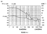
- FIG. 7 is a graph showing the analysis result of the one-round transfer function of the minor feedback loop of the noise reduction device according to the second embodiment.
- the characteristic line G-LM2 shows the gain characteristic with respect to the frequency of the minor feedback loop
- the characteristic line P-LM2 shows the phase characteristic with respect to the frequency of the minor feedback loop.
- the gain on the characteristic line related to the minor feedback loop is defined by the decibel display value of the value measured by the voltage measuring terminal 302 in FIG. 5 divided by the input voltage to the voltage input terminal 301.
- the phase in which the measured voltage at the voltage measuring terminal 302 is completely out of phase with the input voltage to the voltage input terminal 301 is defined as 0 °.
- a state in which the phase of the measured voltage is advanced with respect to the phase of the input voltage is defined as "phase is positive”
- a state in which the phase of the measured voltage is delayed with respect to the phase of the input voltage is defined as "phase is negative”. do.
- the minor feedback loop forms positive feedback. Therefore, it is generally known that when the gain of the minor feedback loop exceeds 0 (dB) in the frequency band forming positive feedback, the minor feedback loop causes closed loop oscillation.
- the feedback control in general negative feedback is as described above, but as will be described later, the inventor has described that even if the phase is in the range of -180 ° to 180 °, it is near -180 ° or 180 °. It has been confirmed that in the vicinity, feedback control is not performed so as to set the control target to 0, and conversely, feedback control is performed so as to increase the control target.
- feedback control is not performed so as to set the control target to 0, and conversely, feedback control is performed so as to increase the control target.
- the function of the intermediate frequency component addition unit 30 shown in FIGS. 1 and 2 is realized.
- the frequency range of 1 (Hz) to 25 (MHz) whose phase is above ⁇ 180 ° and below 180 ° is the negative feedback band, and the phase is ⁇ 180.
- the frequency range higher than 25 (MHz) below ° is the positive feedback band.
- the gain exceeds 0 (dB), so the compensation signal icmp is set to 0. It is understood that feedback control is performed so as to. This is because, in the characteristic line G-AFb of FIG. 6 (b), the gain of the major feedback loop is reduced in the frequency region of 100 (kHz) or less as compared with the characteristic line G-AFa of FIG. 6 (a). It also matches that there is. As described above, due to the action of the inverting amplifier circuit 110, a negative minor feedback loop is formed equivalently for the low frequency signal with respect to the major feedback loop for generating the compensation signal ICMP. As a result, the function of the low frequency component subtraction unit 50 of FIGS. 1 and 2 is realized.
- the gain of 150 (kHz) in the minor feedback loop is about -3.9 (dB), and the phase is about -150 °.
- the characteristic line G-AFb shown in FIG. 6 (b) is around 150 (kHz) as described above. Gain is selectively increased, increasing by up to 5.0 (dB).
- the low frequency component (100 (kHz) or less in the example of FIG. 6) or less is formed by the minor feedback loop by the intermediate frequency component addition unit 30 and the low frequency component subtraction unit 50.
- the intermediate frequency component around 150 (kHz) in the example of FIG. 6
- 100 (kHz) defined as the boundary of the low frequency component corresponds to one embodiment of the "first frequency”
- 150 (kHz) corresponding to the intermediate frequency is the "second frequency”.
- the inverting amplifier circuit 110 corresponds to an embodiment of the "inverting amplifier circuit” common to the intermediate frequency component addition unit 30 and the low frequency component subtraction unit 50.
- the phase adjustment circuit 160 provided in the differential inverting amplifier circuit 150 corresponds to one embodiment of the "first phase adjustment circuit”
- the phase adjustment circuit 120 provided in the inverting amplifier circuit 110 is a "second phase adjustment circuit”.
- the phase adjustment circuit corresponds to one embodiment of the "phase adjustment circuit”.
- Embodiment 3 In the following embodiments, an example of adjusting the frequency characteristics of the minor feedback loop will be described. In the third embodiment, the adjustment for advancing the phase of the minor feedback loop as compared with the second embodiment will be described.
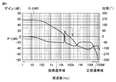
- FIG. 8 is a graph showing the analysis result of the one-round transfer function of the minor feedback loop of the noise reduction device according to the third embodiment.
- the phase adjustment circuit 160 of the differential inverting amplifier circuit 150 in the compensation signal generation unit 60 and the phase adjustment circuit 160 in the compensation signal generation unit 60 are based on the electric circuit of the noise reduction device 10x according to the second embodiment shown in FIG.
- the circuit element constants constituting the phase adjustment circuit 120 of the inverting amplifier circuit 110 intermediate frequency component addition unit 30 and low frequency component subtraction unit 50
- the phase of the minor feedback loop is advanced beyond the characteristics of FIG. There is.
- the characteristic line G-LM3 shows the gain characteristic in the third embodiment
- the characteristic line P-LM3 shows the phase characteristic in the third embodiment. From the characteristic lines G-LM3 and P-LM3, in the third embodiment, the gain at 150 (kHz) is ⁇ 9.8 (dB), and the phase is about -138 °.
- the gain at 150 (kHz) is -3.9 (dB) and the phase is ⁇ 150 °, but in the third embodiment, the gain is lower. And it is understood that the phase is far from ⁇ 180 °.
- the amplification of the intermediate frequency here, around 150 (kHz)
- the function of the intermediate frequency component addition unit 30 is not exhibited.
- FIG. 9 is a graph showing the analysis result of the one-round transfer function of the major feedback loop of the noise reduction device according to the third embodiment.
- FIG. 9A shows an analysis of only the major feedback loop before the application of the present embodiment, that is, with the intermediate frequency component adding section 30 and the low frequency component subtracting section 50 removed, as in FIG. 6A.
- the results are shown.
- the circuit from which the inverting amplifier circuit 110 has been removed is targeted for analysis, thereby performing the above analysis. You can get the result.
- FIG. 9B shows the analysis result at the time of application of the present embodiment, which targets the electric circuit of FIG. 4 in which the circuit constants according to the third embodiment have been adjusted. ..
- the characteristic line G-AF3a shows the gain characteristic with respect to the frequency
- the characteristic line P-AF3a shows the phase characteristic with respect to the frequency
- the characteristic line G-AF3b shows the gain characteristic with respect to the frequency of the major feedback loop
- the characteristic line P-AF3b shows the phase characteristic with respect to the frequency of the major feedback loop.
- a negative feedback band (generally 25 (kHz) to 20 (MHz)) and a positive feedback band are associated with the phases of the characteristic lines P-AF3a and P-AF3b. (Approximately 25 (kHz) or less, or 20 (MHz) or more) exists.
- the inverting amplifier circuit 110 (intermediate frequency component addition unit 30 and low frequency component subtraction unit 50) is arranged.
- the gain is increased by about 2.2 (dB) at the maximum.
- This gain increase is smaller than the increase between the characteristic lines G-AFa and G-AFb in the second embodiment (up to about 5.0 (dB)). That is, as compared with the second embodiment, the function of the intermediate frequency component addition unit 30 is weakened.
- the second embodiment and the third embodiment are equivalent in terms of the effect of reducing the low frequency component (for example, the frequency region of 100 (kHz) or less) by the low frequency component subtracting unit 50.
- the effect of reducing the low frequency component is maintained by adjusting the phase of the minor feedback loop, and the circuit operation is stabilized by suppressing the oscillation by suppressing the gain.
- the second embodiment has a higher noise reduction effect of the frequency component around the intermediate frequency (150 (kHz)).
- Embodiment 4 contrary to the third embodiment, the adjustment for delaying the phase of the minor feedback loop as compared with the second embodiment will be described.
- phase adjustment circuit 160 (inside the differential inverting amplifier circuit 150) and the phase adjustment circuit 120 are based on the electric circuit of the noise reduction device 10x according to the second embodiment shown in FIG.
- the phase of the minor feedback loop is delayed from the characteristics of FIG. 7 by adjusting the circuit element constants (inside the inverting amplifier circuit 110).
- FIG. 10 is a graph showing the analysis result of the one-round transfer function of the minor feedback loop of the noise reduction device according to the fourth embodiment.
- the characteristic line G-LM4 shows the gain characteristic in the fourth embodiment
- the characteristic line P-LM4 shows the phase characteristic in the fourth embodiment.
- the gain at 150 (kHz) is 1.0 (dB)
- the phase is about -171 °. Therefore, in the second embodiment (FIG. 7), the gain is increased in the third embodiment as compared with the case where the gain at 150 (kHz) is -3.9 (dB) and the phase is ⁇ 150 °. And it is understood that the phase is approaching ⁇ 180 °.
- the phase at 150 (kHz) is brought close to -180 ° by phase adjustment so that the frequency region of 200 to 400 (kHz) becomes the positive feedback band.
- the gain is also set slightly higher than 0 (dB).
- the amplification effect of the frequency component around the intermediate frequency (150 (kHz)) corresponding to the function of the intermediate frequency component adding unit 30 is enhanced.
- the phase around 150 (kHz), in which the gain is set slightly higher than 0 (dB) is close to ⁇ 180 ° but not less than ⁇ 180 °, so that oscillation does not occur.
- FIG. 11 is a graph showing the analysis result of the one-round transfer function of the major feedback loop of the noise reduction device according to the fourth embodiment.
- FIG. 11 (a) similarly to FIGS. 6 (a) and 9 (a), before the application of the present embodiment, that is, the intermediate frequency component addition unit 30 and the low frequency component subtraction unit 50 are removed.
- the analysis results for only the major feedback loop are shown. Specifically, in the electric circuit of FIG. 4 in which the circuit constants according to the fourth embodiment described in FIG. 10 have been adjusted, the circuit from which the inverting amplifier circuit 110 has been removed is targeted for analysis, thereby performing the above analysis. You can get the result.
- FIG. 11B shows an analysis result for the electric circuit of FIG. 4 in which the circuit constants according to the fourth embodiment have been adjusted.
- the characteristic line G-AF4a shows the gain characteristic with respect to the frequency
- the characteristic line P-AF4a shows the phase characteristic with respect to the frequency
- the characteristic line G-AF4b shows the gain characteristic with respect to the frequency of the major feedback loop
- the characteristic line P-AF4b shows the phase characteristic with respect to the frequency of the major feedback loop.
- the negative feedback band (generally 25 (kHz) or 50 (kHz) to 20 (MHz)) is associated with the phase on the characteristic lines P-AF4a and P-AF4b. And there is a positive feedback band (25 (kHz) or less, 50 (kHz) or less, or 20 (MHz) or more).
- the inverting amplifier circuit 110 (intermediate frequency component addition unit 30 and low frequency component subtraction unit 50) is arranged.
- the gain is increased by about 18.2 (dB) at the maximum. This gain increase is larger than the gain increase between the characteristic lines G-AFa and G-AFb in the second embodiment (up to about 5.0 (dB)).
- the gain peak around 25 (kHz) is included as compared with the characteristic line G-AF4a of FIG. 11A. It can be read that the gain in the frequency region of 100 (kHz) or less is reduced. Therefore, it is understood that the second embodiment and the fourth embodiment are equivalent in terms of the effect of reducing the low frequency component (for example, the frequency region of 100 (kHz) or less) by the low frequency component subtracting unit 50.
- the effect of reducing the low frequency component is maintained by adjusting the phase of the minor feedback loop, and the frequency component around the intermediate frequency (for example, 150 (kHz)) is maintained.
- a desired characteristic can be obtained by adjusting the one-round transfer function (frequency characteristic) of the minor feedback loop. Specifically, by adjusting the circuit constants of at least one of the phase adjustment circuits 120 and 160, the frequency domain (low frequency) in which the negative minor feedback loop operates and the intermediate frequency in which the positive minor feedback loop operates can be arbitrarily selected. It is possible to set to.
- the fourth embodiment a configuration example capable of maintaining the reduction effect of the low frequency component and enhancing the noise reduction effect of the intermediate frequency component (for example, 150 (kHz)) is shown.
- the measurement results of an actual machine experiment to which the noise reduction device according to the fourth embodiment is applied will be illustrated.
- FIG. 12 is a graph showing the actual measurement result of the noise reduction effect by the noise reduction device according to the fourth embodiment.
- the vertical axis of FIG. 12 shows the noise terminal voltage (dB ⁇ V) measured in the experiment, and the horizontal axis shows the frequency (Hz).
- the noise terminal voltage was measured by quasi-peak detection.
- the characteristic line CEa is a case where the compensation signal generation unit 60 (differential inverting amplifier circuit 150 and emitter follower 180), the intermediate frequency component addition unit 30 and the low frequency component subtraction unit 50 (inverting amplifier circuit 110) are stopped. The noise terminal voltage measurement result is shown.
- the characteristic line CEb operates a compensation signal generation unit 60 (differential inverting amplifier circuit 150 and emitter follower 180), an intermediate frequency component addition unit 30 and a low frequency component subtraction unit 50 (inverting amplifier circuit 110). Further, the noise terminal voltage measurement result during the operation of the noise reduction device according to the fourth embodiment is shown.
- the noise terminal voltage is from 150 (kHz) to 2 (MHz) due to the operation of the compensation signal generation unit 60, the low frequency component subtraction unit 50, and the intermediate frequency component addition unit 30. It is understood that the frequency range is reduced by up to 20 (dB).
- the measurement result of FIG. 12 also corresponds to the one-round transfer function (specifically, the characteristic line G-AF4b) of the major feedback loop shown in FIG. 11 (b). Further, in the frequency band over 2 (MHz) where the gain is 0 (dB) or less on the characteristic line G-AF4b, a significant change in the noise terminal voltage (that is, implementation) is performed from the comparison of the characteristic lines CEa and CEb in FIG. It can be confirmed that the influence of the operation of the noise reduction device according to the fourth embodiment) has not occurred.
- FIG. 13 is an example of an actually measured waveform of the compensation signal icmp in the noise reduction device according to the fourth embodiment.
- the compensation signal icmp was measured in a configuration in which the noise reduction device according to the fourth embodiment was connected to the noise source circuit 11 and the noise leakage circuit 12 similar to those connected in FIG.
- the horizontal axis is the time axis and the vertical axis is the current value of the compensation signal ICMP.
- FIG. 13A similarly to the simulation conditions in FIG. 11A, the intermediate frequency component addition unit 30 and the low frequency component subtraction unit 50 are removed, and then the major feedback loop is formed so that oscillation does not occur.
- FIG. 13 (b) when the intermediate frequency component addition unit 30 and the low frequency component subtraction unit 50 are operated in the same manner as in the simulation conditions in FIG. 11 (b), that is, in the present embodiment.
- the waveform of the compensation signal icmp at the time of application of the form is shown.
- the current waveform of FIG. 13 (b) corresponds to the actual measurement result under the characteristic lines G-AF4b and P-AF4b of FIG. 11 (a).
- an offset current If from the zero point is generated in the compensation signal (current) ICMP.
- the measured value of Iof in the actual machine experiment by the inventor was about -400 (mA).
- Such an offset current If is generated because the offset voltage generated by the operational amplifier 170, the transistors 181 and 182, and the like is applied to the compensation signal injection unit 80.
- the offset current If is a relatively large value even if the applied offset voltage is small. It is easily inferred that
- FIG. 13B it can be confirmed that almost no offset current is generated in the compensation signal icmp. This is because the low frequency offset voltage is compensated by the inverting amplifier circuit 110 (intermediate frequency component addition unit 30 and low frequency component subtraction unit 50). As described above, by reducing the offset, unnecessary power consumption and narrowing of the range of the output current and voltage amplitude of the compensation signal generation unit 60 can be suppressed.
- the intermediate frequency to be noise-reduced can be designed to any frequency by adjusting the one-round transfer function (frequency characteristics) of the minor feedback loop by adjusting the constants of the circuit elements.
- connection line m0, the noise source current input line m1, and the leakage noise current output line m2 are described as two lines, but in application to three-phase alternating current, these m0 ⁇ M2 is 3 lines.
- m0 to m2 may be 4 or more lines.
- the noise reduction device can be connected to any part of the current path between the noise source circuit 11 and the noise leakage circuit 12.
- the noise source circuit 11 and the noise leakage circuit 12 are not particularly limited, and the circular transfer function of the minor feedback loop described above is used so that the intermediate frequency is appropriately set according to the frequency component to be reduced. By adjusting (frequency characteristics), it is possible to suppress the offset signal and oscillation, and reduce the noise of the frequency component.
- the operational amplifier 115 , 170 (the transistor when the differential inverting amplifier circuit 150 or the inverting amplifier circuit 110 is composed of a transistor instead of an operational amplifier) can be further combined with the adjustment of the gain bandwidth product to obtain a desired frequency. be.
- the gain bandwidth product (GB product) of the operational amplifier and / or the transistor it is possible to omit the arrangement of the low-pass filter and configure the phase adjustment circuits 120 and 160.
- 10,10x noise reduction device 11 noise source circuit, 12 noise leakage circuit, 20 noise detector, 21,81 current transformer, 21x, 81y, 81z secondary winding, 21y, 21z, 81x primary winding, 30 intermediate frequency Component adder, 32, 32x, 52, 90, 90x operator, 35 intermediate frequency component extraction circuit, 50 low frequency component subtraction section, 55 low frequency component amplifier circuit, 60 compensation signal generator, 61 input line, 65 amplifier circuit , 70 Compensation signal detection unit, 71 detection resistance, 80 compensation signal injection unit, 100 combined circuit, 110 inverting amplifier circuit, 115, 170 operational amplifier, 120, 160 phase adjustment circuit, 121, 161 negative input resistance, 122, 163 feedback resistance , 123,164 feedback capacitance, 150 differential inverting amplifier circuit, 162 positive input resistance, 180 emitter follower, 181,182 transistor, 201,301 voltage input terminal, 202,302 voltage measurement terminal, 300 open point, LM0 major feedback loop , LN1, LP1 minor feedback loop, amplifier compensation signal, ignd leak
Landscapes
- Engineering & Computer Science (AREA)
- Physics & Mathematics (AREA)
- Power Engineering (AREA)
- Nonlinear Science (AREA)
- Electromagnetism (AREA)
- General Physics & Mathematics (AREA)
- Radar, Positioning & Navigation (AREA)
- Automation & Control Theory (AREA)
- Amplifiers (AREA)
Priority Applications (5)
| Application Number | Priority Date | Filing Date | Title |
|---|---|---|---|
| EP20926528.9A EP4131755B1 (en) | 2020-03-24 | 2020-03-24 | Noise reduction device |
| US17/794,992 US11843384B2 (en) | 2020-03-24 | 2020-03-24 | Noise reduction device |
| CN202080098633.4A CN115298944A (zh) | 2020-03-24 | 2020-03-24 | 噪声降低装置 |
| PCT/JP2020/013042 WO2021192042A1 (ja) | 2020-03-24 | 2020-03-24 | ノイズ低減装置 |
| JP2020541822A JP6811904B1 (ja) | 2020-03-24 | 2020-03-24 | ノイズ低減装置 |
Applications Claiming Priority (1)
| Application Number | Priority Date | Filing Date | Title |
|---|---|---|---|
| PCT/JP2020/013042 WO2021192042A1 (ja) | 2020-03-24 | 2020-03-24 | ノイズ低減装置 |
Publications (1)
| Publication Number | Publication Date |
|---|---|
| WO2021192042A1 true WO2021192042A1 (ja) | 2021-09-30 |
Family
ID=74096343
Family Applications (1)
| Application Number | Title | Priority Date | Filing Date |
|---|---|---|---|
| PCT/JP2020/013042 Ceased WO2021192042A1 (ja) | 2020-03-24 | 2020-03-24 | ノイズ低減装置 |
Country Status (5)
| Country | Link |
|---|---|
| US (1) | US11843384B2 (https=) |
| EP (1) | EP4131755B1 (https=) |
| JP (1) | JP6811904B1 (https=) |
| CN (1) | CN115298944A (https=) |
| WO (1) | WO2021192042A1 (https=) |
Cited By (3)
| Publication number | Priority date | Publication date | Assignee | Title |
|---|---|---|---|---|
| EP4350965A1 (en) * | 2022-10-03 | 2024-04-10 | Toshiba Carrier Corporation | Current injection type active filter and circuit |
| EP4447317A4 (en) * | 2021-12-08 | 2025-01-29 | Mitsubishi Electric Corporation | NOISE FILTER |
| EP4510434A4 (en) * | 2022-04-15 | 2025-07-09 | Em Coretech Inc | ACTIVE VOLTAGE VARIATION COMPENSATION DEVICE |
Families Citing this family (2)
| Publication number | Priority date | Publication date | Assignee | Title |
|---|---|---|---|---|
| JP7288206B2 (ja) * | 2021-09-30 | 2023-06-07 | ダイキン工業株式会社 | ノイズ低減回路、電力変換装置及び冷凍装置 |
| WO2024009489A1 (ja) * | 2022-07-08 | 2024-01-11 | 三菱電機株式会社 | ノイズフィルタ |
Citations (3)
| Publication number | Priority date | Publication date | Assignee | Title |
|---|---|---|---|---|
| JP2002010650A (ja) | 2000-03-28 | 2002-01-11 | Internatl Rectifier Corp | コモンモード電流を低減するための能動フィルタ |
| JP2010057268A (ja) * | 2008-08-28 | 2010-03-11 | Fuji Electric Systems Co Ltd | 伝導性ノイズフィルタ |
| JP2019080469A (ja) * | 2017-10-27 | 2019-05-23 | 三菱電機株式会社 | ノイズ低減装置 |
Family Cites Families (9)
| Publication number | Priority date | Publication date | Assignee | Title |
|---|---|---|---|---|
| US8265769B2 (en) * | 2007-01-31 | 2012-09-11 | Medtronic, Inc. | Chopper-stabilized instrumentation amplifier for wireless telemetry |
| JP2011097186A (ja) * | 2009-10-27 | 2011-05-12 | Panasonic Corp | 負帰還型歪補償装置及び負帰還型歪補償方法 |
| CN102412724B (zh) * | 2011-12-07 | 2013-11-06 | 西安启芯微电子有限公司 | 具有片内频率补偿的电压模dc/dc电路 |
| US20150003124A1 (en) * | 2012-01-27 | 2015-01-01 | Mitsubishi Electric Corporation | High-frequency current reduction device |
| CN105099171B (zh) * | 2014-05-16 | 2018-10-26 | 深圳市中兴微电子技术有限公司 | 一种补偿网络、开关电源电路及电路补偿方法 |
| US10063130B2 (en) * | 2014-09-19 | 2018-08-28 | Intersil Americas LLC | Multi-stage amplifier |
| EP3109987B1 (en) | 2015-06-26 | 2021-04-28 | Mitsubishi Electric R&D Centre Europe B.V. | Active common mode filter device |
| JP6180600B1 (ja) * | 2016-09-02 | 2017-08-16 | 三菱電機株式会社 | 車載エンジン制御装置 |
| US10374510B2 (en) * | 2017-04-07 | 2019-08-06 | Texas Instruments Incorporated | Compensated active electro-magnetic interference filters |
-
2020
- 2020-03-24 JP JP2020541822A patent/JP6811904B1/ja active Active
- 2020-03-24 WO PCT/JP2020/013042 patent/WO2021192042A1/ja not_active Ceased
- 2020-03-24 EP EP20926528.9A patent/EP4131755B1/en active Active
- 2020-03-24 CN CN202080098633.4A patent/CN115298944A/zh active Pending
- 2020-03-24 US US17/794,992 patent/US11843384B2/en active Active
Patent Citations (3)
| Publication number | Priority date | Publication date | Assignee | Title |
|---|---|---|---|---|
| JP2002010650A (ja) | 2000-03-28 | 2002-01-11 | Internatl Rectifier Corp | コモンモード電流を低減するための能動フィルタ |
| JP2010057268A (ja) * | 2008-08-28 | 2010-03-11 | Fuji Electric Systems Co Ltd | 伝導性ノイズフィルタ |
| JP2019080469A (ja) * | 2017-10-27 | 2019-05-23 | 三菱電機株式会社 | ノイズ低減装置 |
Non-Patent Citations (1)
| Title |
|---|
| See also references of EP4131755A4 |
Cited By (4)
| Publication number | Priority date | Publication date | Assignee | Title |
|---|---|---|---|---|
| EP4447317A4 (en) * | 2021-12-08 | 2025-01-29 | Mitsubishi Electric Corporation | NOISE FILTER |
| EP4510434A4 (en) * | 2022-04-15 | 2025-07-09 | Em Coretech Inc | ACTIVE VOLTAGE VARIATION COMPENSATION DEVICE |
| EP4350965A1 (en) * | 2022-10-03 | 2024-04-10 | Toshiba Carrier Corporation | Current injection type active filter and circuit |
| JP2024053311A (ja) * | 2022-10-03 | 2024-04-15 | 株式会社東芝 | 電流注入型アクティブフィルタ及び回路 |
Also Published As
| Publication number | Publication date |
|---|---|
| CN115298944A (zh) | 2022-11-04 |
| JP6811904B1 (ja) | 2021-01-13 |
| EP4131755A1 (en) | 2023-02-08 |
| US20220376684A1 (en) | 2022-11-24 |
| EP4131755A4 (en) | 2023-05-24 |
| EP4131755B1 (en) | 2024-07-17 |
| JPWO2021192042A1 (https=) | 2021-09-30 |
| US11843384B2 (en) | 2023-12-12 |
Similar Documents
| Publication | Publication Date | Title |
|---|---|---|
| JP6811904B1 (ja) | ノイズ低減装置 | |
| JP6491349B2 (ja) | 電力変換装置 | |
| Wang et al. | Investigation of hybrid EMI filters for common-mode EMI suppression in a motor drive system | |
| JP3428588B2 (ja) | コモンモード電流を低減するための能動フィルタ | |
| Di Piazza et al. | An improved active common-mode voltage compensation device for induction motor drives | |
| US9722484B2 (en) | Noise filtering | |
| JP2005532027A (ja) | 能動emiフィルタ | |
| US9231464B2 (en) | Method for reducing the common mode current | |
| JP6803478B1 (ja) | 電力変換装置 | |
| CN102984630A (zh) | 用于音频放大系统中减少失真的系统和方法 | |
| Chang et al. | Research and realization of a novel active common-mode EMI filter | |
| US20170271996A1 (en) | Prevention of switching discontinuity in a hybrid switched mode amplifier | |
| US9496829B2 (en) | Amplifier arrangement comprising a low-pass filter device | |
| JP5810765B2 (ja) | ノイズ低減装置およびこれを備えた電力変換装置 | |
| US20150326180A1 (en) | Control of cross-over point | |
| US20150365059A1 (en) | Class-d amplifier and electronic apparatus | |
| JP2009212902A (ja) | 増幅器 | |
| US20230163681A1 (en) | Electromagnetic interference suppression circuit | |
| JP2009296856A (ja) | 電力変換装置のノイズ低減装置 | |
| WO2021234760A1 (ja) | 電力変換装置 | |
| KR102526738B1 (ko) | 보상 회로를 포함하는 증폭 디바이스 | |
| Jiang et al. | Circuit techniques to overcome class-D audio amplifier limitations in mobile devices | |
| Gunaratnam | Design and simulation of class D amplifier using “ON Semiconductor's” power sense 5 processes | |
| JPH0661753A (ja) | 高効率化低障害電力増幅器 | |
| Ni et al. | Study on EMI of power amplifiers in active magnetic bearing systems |
Legal Events
| Date | Code | Title | Description |
|---|---|---|---|
| ENP | Entry into the national phase |
Ref document number: 2020541822 Country of ref document: JP Kind code of ref document: A |
|
| 121 | Ep: the epo has been informed by wipo that ep was designated in this application |
Ref document number: 20926528 Country of ref document: EP Kind code of ref document: A1 |
|
| NENP | Non-entry into the national phase |
Ref country code: DE |
|
| ENP | Entry into the national phase |
Ref document number: 2020926528 Country of ref document: EP Effective date: 20221024 |