WO2021192042A1 - Noise reduction device - Google Patents
Noise reduction device Download PDFInfo
- Publication number
- WO2021192042A1 WO2021192042A1 PCT/JP2020/013042 JP2020013042W WO2021192042A1 WO 2021192042 A1 WO2021192042 A1 WO 2021192042A1 JP 2020013042 W JP2020013042 W JP 2020013042W WO 2021192042 A1 WO2021192042 A1 WO 2021192042A1
- Authority
- WO
- WIPO (PCT)
- Prior art keywords
- compensation signal
- noise
- frequency component
- unit
- phase
- Prior art date
Links
Images


Classifications
-
- H—ELECTRICITY
- H03—ELECTRONIC CIRCUITRY
- H03K—PULSE TECHNIQUE
- H03K5/00—Manipulating of pulses not covered by one of the other main groups of this subclass
- H03K5/125—Discriminating pulses
- H03K5/1252—Suppression or limitation of noise or interference
-
- G—PHYSICS
- G05—CONTROLLING; REGULATING
- G05F—SYSTEMS FOR REGULATING ELECTRIC OR MAGNETIC VARIABLES
- G05F1/00—Automatic systems in which deviations of an electric quantity from one or more predetermined values are detected at the output of the system and fed back to a device within the system to restore the detected quantity to its predetermined value or values, i.e. retroactive systems
- G05F1/10—Regulating voltage or current
-
- H—ELECTRICITY
- H02—GENERATION; CONVERSION OR DISTRIBUTION OF ELECTRIC POWER
- H02J—CIRCUIT ARRANGEMENTS OR SYSTEMS FOR SUPPLYING OR DISTRIBUTING ELECTRIC POWER; SYSTEMS FOR STORING ELECTRIC ENERGY
- H02J1/00—Circuit arrangements for dc mains or dc distribution networks
- H02J1/02—Arrangements for reducing harmonics or ripples
-
- H—ELECTRICITY
- H02—GENERATION; CONVERSION OR DISTRIBUTION OF ELECTRIC POWER
- H02M—APPARATUS FOR CONVERSION BETWEEN AC AND AC, BETWEEN AC AND DC, OR BETWEEN DC AND DC, AND FOR USE WITH MAINS OR SIMILAR POWER SUPPLY SYSTEMS; CONVERSION OF DC OR AC INPUT POWER INTO SURGE OUTPUT POWER; CONTROL OR REGULATION THEREOF
- H02M1/00—Details of apparatus for conversion
- H02M1/12—Arrangements for reducing harmonics from ac input or output
-
- H—ELECTRICITY
- H02—GENERATION; CONVERSION OR DISTRIBUTION OF ELECTRIC POWER
- H02M—APPARATUS FOR CONVERSION BETWEEN AC AND AC, BETWEEN AC AND DC, OR BETWEEN DC AND DC, AND FOR USE WITH MAINS OR SIMILAR POWER SUPPLY SYSTEMS; CONVERSION OF DC OR AC INPUT POWER INTO SURGE OUTPUT POWER; CONTROL OR REGULATION THEREOF
- H02M7/00—Conversion of ac power input into dc power output; Conversion of dc power input into ac power output
- H02M7/42—Conversion of dc power input into ac power output without possibility of reversal
- H02M7/44—Conversion of dc power input into ac power output without possibility of reversal by static converters
- H02M7/48—Conversion of dc power input into ac power output without possibility of reversal by static converters using discharge tubes with control electrode or semiconductor devices with control electrode
-
- H—ELECTRICITY
- H03—ELECTRONIC CIRCUITRY
- H03K—PULSE TECHNIQUE
- H03K5/00—Manipulating of pulses not covered by one of the other main groups of this subclass
- H03K2005/00286—Phase shifter, i.e. the delay between the output and input pulse is dependent on the frequency, and such that a phase difference is obtained independent of the frequency
Definitions
- This disclosure relates to a noise reduction device.
- noise electromagnetic noise generated from power electronics equipment
- a noise reduction device such as a transistor and an operational amplifier
- the basic configuration of an active filter is usually a function of detecting noise to be reduced existing in the main circuit, a function of generating a compensation voltage or a compensation current for reducing the detected noise by an active element, and a function of generating a compensation current or a compensation current by the active element.
- the ability to inject the generated compensating voltage or compensating current into the main circuit is required.
- an active filter for reducing the common mode current an active filter including a buffer amplifier in which the output of a current transformer that monitors the common mode current is input is used. , A configuration for generating a compensating current is disclosed.
- Patent Document 1 does not mention a method of suppressing a signal that amplifies noise due to a phase delay generated in a compensation current. Further, as described in Patent Document 1, there are a feedback control method and a feedforward control method as control methods related to noise reduction of an active filter.
- the noise amplification signal caused by the phase delay only amplifies the noise existing in the main circuit as it is.
- the noise amplification signal caused by the phase delay brings about positive feedback of noise and oscillates the active filter to destabilize the operation. Therefore, in the feedback control method, it is particularly desired to suppress the noise amplification signal due to the phase lag.
- the feedback control type active filter it is required to increase the gain of the feedback loop in order to enhance the noise reduction effect, but the increase of the gain may also increase the noise amplification signal due to the phase lag. There is. Therefore, in the feedback control type active filter, it tends to be difficult to obtain a high noise reduction effect while suppressing oscillation.
- the present disclosure has focused on the above problems, and an object of the present disclosure is to provide a feedback control type noise reduction device having high stability and a high noise reduction effect.
- the noise reduction device includes a noise detection unit, a compensation signal generation unit, a compensation signal injection unit, a compensation signal detection unit, a low frequency component subtraction unit, and an intermediate frequency component addition unit.
- the noise detection unit detects electromagnetic noise on the connecting line.
- the compensation signal generation unit generates a compensation signal for canceling electromagnetic noise based on the detection signal of the noise detection unit.
- the compensation signal injection unit injects the compensation signal into the connecting line.
- the compensation signal detection unit detects the compensation signal.
- the low frequency component subtraction unit amplifies the first frequency component of the first frequency region lower than the predetermined first frequency among the detection signals by the compensation signal detection unit, and negatively affects the compensation signal generation unit.
- the intermediate frequency component addition unit positively feeds back the component of the predetermined second frequency higher than the first frequency of the detection signals by the compensation signal detection unit to the compensation signal generation unit.
- the noise reduction effect of the second frequency is enhanced, and the effect of reducing the noise of the second frequency is enhanced.
- a feedback control type noise reduction device with high stability can be realized.
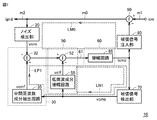
- FIG. 2 It is a control block diagram of the noise reduction apparatus which concerns on Embodiment 1.
- FIG. 2 is a control block diagram of the noise reduction apparatus which concerns on Embodiment 2.
- FIG. 2 is an electric circuit diagram for realizing the control block diagram of FIG. 2 by hardware. It is an electric circuit diagram for evaluating the one-circle transfer function of the major feedback loop of the noise reduction apparatus shown in FIG. It is an electric circuit diagram for evaluating the one-circle transfer function of the minor feedback loop of the noise reduction apparatus shown in FIG. It is a graph which shows the analysis result of the one-circle transfer function of the major feedback loop of the noise reduction apparatus which concerns on Embodiment 2.
- FIG. 2 It is a graph which shows the analysis result of the one-circle transfer function of the minor feedback loop of the noise reduction apparatus which concerns on Embodiment 2.
- FIG. It is a graph which shows the analysis result of the one-circle transfer function of the minor feedback loop of the noise reduction apparatus which concerns on Embodiment 3.
- FIG. It is a graph which shows the analysis result of the one-circle transfer function of the major feedback loop of the noise reduction apparatus which concerns on Embodiment 3.
- FIG. It is a graph which shows the analysis result of the one-circle transfer function of the minor feedback loop of the noise reduction apparatus which concerns on Embodiment 4.
- FIG. It is a graph which shows the analysis result of the one-circle transfer function of the major feedback loop of the noise reduction apparatus which concerns on Embodiment 4.
- FIG. It is a graph which shows the actual measurement result of the noise reduction effect by the noise reduction apparatus which concerns on Embodiment 4. This is an example of an actually measured waveform of a compensation signal in the noise reduction device according to
- FIG. 1 is a control block diagram of the noise reduction device according to the first embodiment.
- the noise reduction device 10 includes a noise detection unit 20, an intermediate frequency component addition unit 30, a low frequency component subtraction unit 50, a compensation signal generation unit 60, and a compensation signal detection unit 70.
- a compensation signal injection unit 80 and a connection line m0 are provided.
- connection line m0 is connected to the noise source current input line m1 for inputting the noise source current icm via the subtractor type operator 90.
- the compensation signal injection unit 80 is connected to the connection line m0 via a subtractor type operator 90.
- the noise detection unit 20 is connected to the connection line m0 in a manner of sandwiching the connection line m0 together with the subtractor type operator 90. As will be described later, the noise detection unit 20 can be configured by a current transformer or a capacitor. Further, the noise detection unit 20 is connected to the leakage noise current output line m2 that outputs the leakage noise current ignd on the opposite side of the connection side from the connection line m0. The noise detection unit 20 outputs a detection voltage vsns that changes according to the current of the connection line m0. Therefore, the detected voltage vsns contains an electromagnetic noise component.
- the intermediate frequency component addition unit 30 includes an adder type operator 32 and an intermediate frequency component extraction circuit 35.
- the intermediate frequency component addition unit 30 is connected to the input line 61 of the compensation signal generation unit via a subtractor type operator 52 in the low frequency component subtraction unit 50.
- the low frequency component subtraction unit 50 includes a subtractor type operator 52 and a low frequency component amplifier circuit 55.
- the low-frequency component amplifier circuit 55 is connected to the input line 61 of the compensation signal generation unit via a subtractor type operator 52.
- the compensation signal generation unit 60 includes an amplifier circuit 65.
- the amplifier circuit 65 amplifies the voltage of the input line 61 to generate a compensation signal ICMP corresponding to the compensation current.
- the compensation signal detection unit 70 outputs a compensation signal detection voltage vcmp according to the compensation signal icmp.
- the intermediate frequency component addition unit 30 generates an output signal vcmf obtained by extracting a predetermined intermediate frequency component from the compensation signal detection voltage vcmp.
- the low-frequency component amplifier circuit 55 generates an output signal vclf from which a low-frequency component having a compensation signal detection voltage vcmp is extracted.
- the noise reduction device 10 forms a feedback loop LM0 via a connection line m0, a noise detection unit 20, a compensation signal generation unit 60, a compensation signal injection unit 80, and a subtractor type operator 90.
- this feedback loop is defined as a “major feedback loop”.
- the compensation signal icmp injected by the subtractor type operator 90 is generated so as to cancel the electromagnetic noise component.
- electromagnetic noise remains on the connection line m0 as a residual deviation depending on the magnitude of the gain of the major feedback loop.
- the compensation signal detection voltage vcmp from the compensation signal detection unit 70 is input to the low frequency component amplifier circuit 55.
- the low frequency component subtraction unit 50 forms a feedback loop LN1 via the low frequency component amplifier circuit 55, the subtractor type operator 52, the compensation signal generation unit 60, and the compensation signal detection unit 70.
- negative feedback is formed by the subtractor type operator 52, so the feedback loop is defined below as a "negative minor feedback loop”.
- the negative minor feedback loop LN1 feedback control is performed so that the low frequency component in the compensation signal ICMP corresponding to the one-round transfer function (frequency characteristic) of the negative minor feedback loop is set to 0 by forming the negative feedback. It is said.
- the low frequency component in the compensation signal icmp causes unnecessary power consumption or narrows the amplitude of the voltage and current output in the compensation signal generation unit 60. Furthermore, there is a concern that forming positive feedback in the major feedback loop may cause closed-loop oscillation.
- the compensation signal detection voltage vcmp from the compensation signal detection unit 70 is input to the intermediate frequency component extraction circuit 35.
- the intermediate frequency component addition unit 30 forms the feedback loop LP1 via the intermediate frequency component extraction circuit 35, the adder type operator 32, the compensation signal generation unit 60, and the compensation signal detection unit 70.
- the feedback loop LP1 positive feedback is formed by the adder type operator 32. Therefore, the feedback loop is defined below as a “positive minor feedback loop”.
- feedback control is performed so as to amplify the intermediate frequency component in the compensation signal imp according to the one-round transfer function (frequency characteristic) of the positive minor feedback loop by forming the positive feedback. It is said.
- the intermediate frequency can be variably set by adjusting the one-round transfer function (frequency characteristic) of the positive minor feedback loop LP1. Therefore, by adjusting the circular transfer function of the positive minor feedback loop LP1 so that the intermediate frequency is set to an arbitrary frequency to be noise-reduced, the noise reduction device 10 has a high noise reduction effect at an arbitrary frequency. Can be demonstrated.
- the gain of the positive minor feedback loop LP1 generally needs to be less than 1.
- the positive minor feedback loop LP1 causes closed-loop oscillation, so that a signal equal to or larger than the input limit value is input to the compensation signal generation unit 60 or the like, and a desired noise reduction operation is performed. This is because there is a risk that
- the major feedback loop LM0 under the action of the positive minor feedback loop LP1 and the negative minor feedback loop LN1, the major feedback loop LM0 generates a compensation signal imp that acts as a noise canceling component.
- the compensation signal icmp the component of the frequency (intermediate frequency) to be reduced by the noise is amplified by the positive minor feedback loop LP1, and the low frequency component is reduced by the negative minor feedback loop LN1. It will be generated.
- the low frequency component (including the offset component) of the compensation signal impp is suppressed to reduce the power consumption and stabilize the operation, and then the intermediate frequency component is used. A high noise reduction effect due to amplification can be obtained.
- FIG. 2 is a control block diagram of the noise reduction device 10x according to the second embodiment.
- the noise reduction device 10x according to the second embodiment corresponds to a device in which the control block of the noise reduction device 10 shown in FIG. 1 is modified into a configuration suitable for mounting.
- the noise reduction device 10x according to the second embodiment is different from the noise reduction device 10 shown in FIG. 1 in the following points.
- the compensation signal generation unit 60 further has a reverse phase conversion element 66 in addition to the amplifier circuit 65. Therefore, in FIG. 2, the phase of the compensation signal icmp output from the compensation signal generation unit 60 is inverted from that of the compensation signal icmp in FIG.
- An adder type operator 90x is arranged on the connection line m0 instead of the subtractor type operator 90 in FIG. Therefore, the compensation signal icmp from the compensation signal generation unit 60 is injected into the connection line m0 via the adder type operator 90x.
- the intermediate frequency component addition unit 30 further includes a phase inversion element 33 and a reverse phase conversion element 34 in addition to the intermediate frequency component extraction circuit 35. Further, instead of the adder type operator 32, the subtractor type operator 32x is arranged. The output signal vcmf of the intermediate frequency component extraction circuit 35 is input to the ⁇ side of the operator 32x after the antiphase conversion and the phase inversion.
- the low frequency component subtraction unit 50 further includes a reverse phase conversion element 53 in addition to the subtractor type operator 52 and the low frequency component amplifier circuit 55.
- the output signal vclf of the low-frequency component amplifier circuit 55 is input to the ⁇ side of the operator 52 after the reverse phase conversion.
- the reverse phase conversion elements 34, 53, 66 can be configured by using, for example, an inverting amplifier circuit composed of an operational amplifier or a transistor. Further, the phase inversion element 33 can be configured by utilizing the phase inversion that occurs as a result of adjusting the phase lag at a high frequency of the operational amplifier or the transistor.
- the phase of the compensation signal icmp from the compensation signal generation unit 60 is inverted as compared with the control configuration of FIG.
- the compensation signal ICMP is injected into the connection line m0 via the adder type operator 90x instead of the subtractor type operator 90 in FIG. Therefore, it is understood that the compensation signal ICMP injected into the connection line m0 has the same phase between FIGS. 1 and 2.
- the phase of the compensation signal detection voltage vcmp from the compensation signal detection unit 70 is also inverted from that of FIG.
- the output signal vclf of the low frequency component amplifier circuit 55 is input to the subtractor type operator 52 (-side) after the reverse phase conversion. Therefore, it is understood that the sign (positive / negative) of the compensation signal detection voltage vcmp acting on the calculation by the operator 52 is the same in FIGS. 1 and 2.
- the output signal vcmf generated by the intermediate frequency component extraction circuit 35 from the compensation signal detection voltage vcmp whose phase is inverted from FIG. 1 is further phase inverted after reverse phase conversion, and is a subtractor type. It is input to the operator 32x (-side) of. Therefore, the sign (positive / negative) of the compensation signal detection voltage vcmp acting on the calculation is the same between the operator 32 (adder type) in FIG. 1 and the operator 32x (subtractor type) in FIG. Is understood to be.
- the symbols of the signal vcmf and the output signal vclf related to the low frequency are the same. Therefore, it is understood that the noise reduction device 10x of FIG. 2 and the noise reduction device 10 of FIG. 1 realize the same control contents.
- the operator 52 in the low frequency component subtraction unit 50 and the operator 32x in the intermediate frequency component addition unit 30 can both be configured by the subtractor type, so that they are hardware. It is possible to combine them into a common circuit at the time of mounting.
- the adder type operator 90x to the connection line m0, the options of the hardware constituting the compensation signal injection unit 80 are increased.
- FIG. 3 is an electric circuit diagram for realizing the control block diagram of the noise reduction device 10x shown in FIG. 2 by hardware.
- the noise reduction device 10x includes a connection line m0, a noise detection unit 20, a compensation signal generation unit 60, a compensation signal injection unit 80, a compensation signal detection unit 70, and an intermediate frequency.
- a dual-purpose circuit 100 having the functions of the component addition unit 30 and the low frequency component subtraction unit 50 is provided.
- the noise source circuit 11 that generates the noise source current icm shown in FIG. 1 is connected to the noise source current input line m1.
- the noise source circuit 11 is, for example, an inverter circuit, and generates a noise source current by switching semiconductor elements for power conversion.
- a noise leakage circuit 12 is connected to the leakage noise current output line m2.
- the noise leakage circuit 12 is a general term for a group of circuits that may malfunction due to the inflow of noise, and is, for example, an IC (Integrated Circuit), a system power supply that constitutes a power supply path to the IC, or the like.
- the voltage of the system power supply is AC / DC converted by a rectifying circuit, and then DC / AC conversion is performed from an inverter circuit to a motor or the like.
- the inverter circuit of the one electric device becomes the noise source circuit 11, and the noise generated by the inverter circuit passes through the rectifier circuit and the system power supply and is a component of the other electric device.
- the leakage circuit 12 for example, IC or the like.
- connection line m0 the noise source current input line m1
- leakage noise current output line m2 the leakage noise current output line m2
- the noise detection unit 20 is composed of a current transformer 21.
- the current transformer 21 has primary windings 21y and 21z inserted in the connection line m0 and secondary windings 21x.
- the primary windings 21y and 21z and the secondary winding 21x are magnetically coupled, and the voltage that changes according to the current flowing through the connection line m0 is the secondary winding as the detection voltage vsns shown in FIG. Occurs at 21x.
- the detected voltage vsns includes a voltage component that reflects an electromagnetic noise component in the current of the connection line m0.
- the compensation signal injection unit 80 is composed of a current transformer having a primary winding 81x and secondary windings 81y and 81z that are magnetically coupled to each other.
- the secondary windings 81y and 81z are inserted in the connecting line m0.
- the compensation signal icmp which is the output current of the compensation signal generation unit 60, flows through the primary winding 81x.
- the noise detection unit 20 can be configured by a capacitor as is known. Further, the signal injection unit 80 can also be applied with a capacitor by adopting the control configuration of FIG. 2 using the adder type operator 90x.
- the compensation signal generation unit 60 includes a differential inverting amplifier circuit 150 and an emitter follower 180.
- the differential inverting amplifier circuit 150 includes an operational amplifier 170 and a phase adjusting circuit 160 of the operational amplifier 170.
- the phase adjusting circuit 160 has a negative input resistor 161 and a feedback resistor 163, and a feedback capacitance 164. Further, a positive input resistor 162 is connected to the input terminal (+ side) of the operational amplifier 170.
- the phase adjustment circuit 160 is connected between the input terminal (-side) of the operational amplifier 170 and the output terminal.
- the phase adjustment circuit 160 can adjust the phase difference between the input and output of the differential inverting amplifier circuit 150.
- a low-pass filter is composed of a negative input resistor 161, a feedback resistor 163, and a feedback capacitance 164.
- the emitter follower 180 has transistors 181 and 182 having control electrodes connected to the output terminal of the operational amplifier 170. Transistors 181 and 182 are connected in series between a positive power supply node (V +) and a negative power supply node (V ⁇ ). Compensation signal icmp, which is the output of the compensation signal generation unit 60, is generated at the connection node of the transistors 181 and 182. By connecting the primary winding 81x of the current transformer 81 between the connection nodes of the transistors 181 and 182 and the ground (GND), as shown in FIG. 2, the connection line is passed through the signal injection unit 80. The compensation signal icmp can be injected into m0.
- the arrangement of the emitter follower 180 can be omitted.
- the differential inverting amplifier circuit 150 can be configured by using transistors without using operational amplifiers.
- a detection resistor 71 constituting the compensation signal detection unit 70 is connected between the primary winding 81x of the current transformer 81 and the ground (GND). As a result, a compensation signal detection voltage vcmp proportional to the current value of the compensation signal icmp is generated in the detection resistor 71.
- the dual-purpose circuit 100 having the functions of the intermediate frequency component addition unit 30 and the low frequency component subtraction unit 50 is composed of an inverting amplifier circuit 110.
- the inverting amplifier circuit 110 includes an operational amplifier 115 and a phase adjusting circuit 120 of the operational amplifier 115.
- the phase adjusting circuit 120 has a negative input resistor 121, a feedback resistor 122, and a feedback capacitance 123.
- the phase adjustment circuit 120 can adjust the phase difference between the input and output of the inverting amplifier circuit 110.
- a low-pass filter is composed of a negative input resistor 121, a feedback resistor 122, and a feedback capacitance 123.
- a negative input resistor 121 and a detection resistor 71 are input between the input terminals of the operational amplifier 115.
- the input voltage of the operational amplifier 115 is set to the compensation signal detection voltage vcmp, and as shown in FIG. 2, the compensation signal detection voltage vcmp is the intermediate frequency component addition unit 30 and the low frequency component subtraction unit 50. Will be entered in.
- the output terminal of the inverting amplifier circuit 110 is connected to the input terminal (+ side) of the operational amplifier 170 of the compensation signal generation unit 60. Therefore, the differential inverting amplifier circuit 150 amplifies the voltage difference between the detection voltage vsns from the noise detection unit 20 and the output signal of the inverting amplifier circuit 110 to generate a compensation signal icmp. This constitutes a minor loop of the compensation signal icmp.
- the inverting amplifier circuit 110 can also be configured by using a transistor without using an operational amplifier.
- the operational amplifiers 115 and 170 and the transistors 181, 182 operate by receiving the supply of the power supply voltage V + (positive voltage) and V- (negative voltage).
- the power supply voltages V + and V- can be supplied by a positive direct current power supply PS + and a negative direct current power supply PS- connected in series via ground (GND).
- Each of the DC power supplies PS + and PS- can be configured by a DC stabilized power supply that outputs a positive voltage.
- a DC power supply can be obtained by rectifying the AC current flowing through the noise leakage circuit 12 and supplying it to a switching power supply circuit (not shown).
- both functions of the antiphase conversion elements 34 and 53 in FIG. 2 are realized.
- the function of the reverse phase conversion element 66 in FIG. 2 is realized by the inverting amplification of the differential inverting amplifier circuit 150.
- the function of the phase inversion element 33 in FIG. 2 is realized by adjusting the phase delay of the inverting amplifier circuit 110 by adjusting the circuit constant of the phase adjustment circuit 120. Specifically, it can be realized by adding a phase delay of ⁇ 180 ° to the frequency component corresponding to the intermediate frequency.
- the noise reduction device 10x forms a major feedback loop LM0 via the connection line m0, the noise detection unit 20, the compensation signal generation unit 60, and the compensation signal injection unit 80.
- the major feedback loop LM0 since the differential inverting amplifier circuit 150 forms negative feedback, feedback control is executed so as to eliminate the electromagnetic noise existing in the connection line m0.
- electromagnetic noise remains on the connection line m0 as a residual deviation according to the magnitude of the gain of the major feedback loop LM0.
- the gain of the major feedback loop LM0 is determined by setting the turns ratio between the primary windings 21y and 21z and the secondary winding 21x in the noise detection unit 20 or adjusting the gain of the differential inverting amplifier circuit 150 in the compensation signal generation unit 60. , Can be made larger.
- a minor feedback loop is formed via an inverting amplifier circuit 110 that integrally constitutes an intermediate frequency component addition unit 30 and a low frequency component subtraction unit 50, a compensation signal generation unit 60, and a compensation signal detection unit 70.
- the minor feedback loop forms negative feedback
- feedback control is performed so that the low frequency component in the compensation signal ICMP corresponding to the one-round transfer function (frequency characteristic) of the minor feedback loop is set to zero.
- the minor feedback loop forms positive feedback by generating a signal whose phase is inverted at a certain frequency or higher according to the circular transfer function (frequency characteristic) of the minor feedback loop.
- feedback control can be performed so as to amplify the intermediate frequency component in the compensation signal imp according to the one-round transfer function (frequency characteristic) of the minor feedback loop.
- the frequency regions of the one-round transmission function (frequency characteristics) of the minor feedback loop are different from each other. It is possible to equivalently form the positive minor feedback loop LP1 for the intermediate frequency and the negative minor feedback loop LN1 for the low frequency component in FIGS. 1 and 2.
- the round transfer function (frequency characteristics) of the minor feedback loop should be adjusted so that the frequency domain (intermediate frequency) in which the equivalently positive minor feedback loop is formed corresponds to an arbitrary frequency to be noise-reduced. Therefore, a high noise reduction effect can be exhibited at any frequency.
- the gain of the positive minor feedback loop needs to be less than 1. This is because when the gain is 1 or more, closed-loop oscillation occurs in the positive feedback.
- the one-round transfer function (frequency characteristic) of the minor feedback loop can be adjusted so that a negative minor feedback loop is formed equivalently. This can bring about the effects of suppressing unnecessary power consumption in the major feedback loop LM0, securing the amplitudes of the voltage and current outputs, and stabilizing the operation by suppressing the closed loop oscillation.
- the circular transmission function (frequency characteristic) of the minor feedback loop, the gain of the positive minor feedback loop, and the intermediate frequency in FIG. 3 are the compensation signal generation unit 60, the compensation signal detection unit 70, and the intermediate frequency component addition unit 30. And, by adjusting the circuit constant in the low frequency component subtraction unit 50 (inverting amplifier circuit 110), it can be changed to an arbitrary characteristic.
- FIG. 4 is an electric circuit diagram for evaluating the one-round transfer function of the major feedback loop of the noise reduction device 10x shown in FIG.
- the wiring between the noise detection unit 20 and the negative input resistor 161 in the compensation signal generation unit 60 is opened to input a voltage.
- a terminal 201 and a voltage measurement terminal 202 are provided.
- a circuit transfer function of a major feedback loop was obtained by circuit simulation using such a circuit as an analysis target.
- the voltage input terminal 201 is provided on the negative input resistor 161 side
- the voltage measurement terminal 202 is provided on the noise detection unit 20 side.
- the minor feedback loop by the inverting amplifier circuit 110 was set as a closed loop.
- a voltage corresponding to the current of the connection line m0 into which the compensation signal imp is injected which is provided with the minor feedback loop by the inverting amplifier circuit 110 and is generated by the compensation signal generation unit 60, is generated.
- the main circuit was in a non-powered state.
- the major feedback loop to be analyzed in FIG. 4 corresponds to an embodiment of the “first feedback loop”.
- FIG. 5 is an electric circuit diagram for evaluating the one-round transfer function of the minor feedback loop of the noise reduction device 10x shown in FIG.
- the wiring between the noise detection unit 20 and the negative input resistor 161 in the compensation signal generation unit 60 is opened as in FIG. A point 300 is provided. Further, a circuit provided with a voltage input terminal 301 and a voltage measurement terminal 302 by opening the wiring between the compensation signal injection unit 80 (primary winding 81x) and the output node of the compensation signal generation unit 60 is simulated. Was the subject of analysis.
- the compensation signal injection unit 80 (primary winding 81x) is provided with a voltage input terminal 301, and the compensation signal generation unit 60 side is provided with a voltage measurement terminal 302.
- both the major feedback loop and the minor feedback loop are open loops.
- the main circuit was also in a non-powered state.
- the minor feedback loop analyzed in FIG. 5 corresponds to an embodiment of the “second feedback loop”.
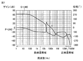
- FIG. 6 is a graph showing the analysis result of the one-round transfer function of the major feedback loop of the noise reduction device according to the second embodiment.
- FIG. 6A shows the analysis result only for the major feedback loop by the compensation signal generation unit 60 in which the intermediate frequency component addition unit 30 and the low frequency component subtraction unit 50 are removed in the control block diagram of FIG.
- This analysis target corresponds to a configuration in which the inverting amplifier circuit 110 is removed from the configuration of FIG.
- the characteristic line G-AFa shows the gain characteristic with respect to the frequency
- the characteristic line P-AFa shows the phase characteristic with respect to the frequency.
- the configuration to which the intermediate frequency component addition unit 30 and the low frequency component subtraction unit 50 in FIG. 6A and the like are not applied is also referred to as a configuration “before application of the present embodiment”.
- FIG. 6B shows an analysis result for the circuit configuration of FIG. 4, including the intermediate frequency component addition unit 30 and the low frequency component subtraction unit 50.
- the characteristic line G-AFb shows the gain characteristic with respect to the frequency of the major feedback loop
- the characteristic line P-AFb shows the phase characteristic with respect to the frequency of the major feedback loop.
- the gain on the characteristic line related to the major feedback loop is defined by the decibel display value of the value obtained by dividing the measured voltage at the voltage measuring terminal 202 in FIG. 4 by the input voltage to the voltage input terminal 201.
- the phase in which the measured voltage at the voltage measuring terminal 202 is completely out of phase with the input voltage to the voltage input terminal 201 is defined as 0 °.
- a state in which the phase of the measured voltage at the voltage measuring terminal 202 is ahead of the phase of the input voltage to the voltage input terminal 201 is “positive in phase”, and a state in which the phase of the measured voltage is behind the phase of the input voltage. Is defined as "phase is negative".
- the major feedback loop forms negative feedback to reduce the electromagnetic noise present at the connection line m0 to zero. Feedback control is feasible.
- the major feedback loop when the phase is below ⁇ 180 ° or above 180 °, the major feedback loop will form positive feedback. It is generally known that when the gain of the major feedback loop exceeds 0 (dB) in the frequency band forming positive feedback, the major feedback loop causes closed loop oscillation.
- the frequency range of about 25 (kHz) to 20 (MHz) corresponds to the phase range of ⁇ 180 ° to 180 ° of the characteristic line P—AFa, which is the negative feedback band. ..
- the frequency range of 25 (kHz) or less and 20 (MHz) or more is a positive feedback band.
- the gain of the positive feedback band exceeds 0 (dB) in the vicinity of 25 (kHz). Includes the frequency domain. Therefore, it can be read that the major feedback loop causes closed loop oscillation in the frequency domain. Therefore, it is understood that it is not easy to obtain a high gain at a desired frequency while suppressing closed-loop oscillation in the configuration before the application of the present embodiment.
- the positive feedback band and the negative feedback band are determined from the characteristic line P-AFb in the same manner as described with reference to FIG. 6 (a).
- the gain is reduced by about 20 (dB) in the vicinity of 25 (kHz) corresponding to the gain peak in FIG. 6 (a), and as a result, the gain peak is reduced. Is made lower than 0 (dB). As a result, it is understood that the closed loop oscillation in the major feedback loop is suppressed in the configuration of the present embodiment.
- the gain around 150 kHz is selectively selected by the effects of the intermediate frequency component adding section 30 and the low frequency component subtracting section 50. It is increased by about 5.0 (dB) at the maximum.
- the frequency component around 150 (kHz) corresponding to the intermediate frequency is enhanced.
- it can be expected that the noise reduction effect of the frequency component corresponding to the intermediate frequency is enhanced.
- the intermediate frequency (around 150 (kHz) above) that selectively increases the gain is arbitrary by adjusting the one-round transfer function (frequency characteristic) of the minor feedback loop by adjusting the constant of the circuit element, as will be described later. It is possible to design at the frequency of. That is, it is also possible to design a noise reduction device by specializing in a frequency region other than around 150 (kHz).
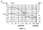
- FIG. 7 is a graph showing the analysis result of the one-round transfer function of the minor feedback loop of the noise reduction device according to the second embodiment.
- the characteristic line G-LM2 shows the gain characteristic with respect to the frequency of the minor feedback loop
- the characteristic line P-LM2 shows the phase characteristic with respect to the frequency of the minor feedback loop.
- the gain on the characteristic line related to the minor feedback loop is defined by the decibel display value of the value measured by the voltage measuring terminal 302 in FIG. 5 divided by the input voltage to the voltage input terminal 301.
- the phase in which the measured voltage at the voltage measuring terminal 302 is completely out of phase with the input voltage to the voltage input terminal 301 is defined as 0 °.
- a state in which the phase of the measured voltage is advanced with respect to the phase of the input voltage is defined as "phase is positive”
- a state in which the phase of the measured voltage is delayed with respect to the phase of the input voltage is defined as "phase is negative”. do.
- the minor feedback loop forms positive feedback. Therefore, it is generally known that when the gain of the minor feedback loop exceeds 0 (dB) in the frequency band forming positive feedback, the minor feedback loop causes closed loop oscillation.
- the feedback control in general negative feedback is as described above, but as will be described later, the inventor has described that even if the phase is in the range of -180 ° to 180 °, it is near -180 ° or 180 °. It has been confirmed that in the vicinity, feedback control is not performed so as to set the control target to 0, and conversely, feedback control is performed so as to increase the control target.
- feedback control is not performed so as to set the control target to 0, and conversely, feedback control is performed so as to increase the control target.
- the function of the intermediate frequency component addition unit 30 shown in FIGS. 1 and 2 is realized.
- the frequency range of 1 (Hz) to 25 (MHz) whose phase is above ⁇ 180 ° and below 180 ° is the negative feedback band, and the phase is ⁇ 180.
- the frequency range higher than 25 (MHz) below ° is the positive feedback band.
- the gain exceeds 0 (dB), so the compensation signal icmp is set to 0. It is understood that feedback control is performed so as to. This is because, in the characteristic line G-AFb of FIG. 6 (b), the gain of the major feedback loop is reduced in the frequency region of 100 (kHz) or less as compared with the characteristic line G-AFa of FIG. 6 (a). It also matches that there is. As described above, due to the action of the inverting amplifier circuit 110, a negative minor feedback loop is formed equivalently for the low frequency signal with respect to the major feedback loop for generating the compensation signal ICMP. As a result, the function of the low frequency component subtraction unit 50 of FIGS. 1 and 2 is realized.
- the gain of 150 (kHz) in the minor feedback loop is about -3.9 (dB), and the phase is about -150 °.
- the characteristic line G-AFb shown in FIG. 6 (b) is around 150 (kHz) as described above. Gain is selectively increased, increasing by up to 5.0 (dB).
- the low frequency component (100 (kHz) or less in the example of FIG. 6) or less is formed by the minor feedback loop by the intermediate frequency component addition unit 30 and the low frequency component subtraction unit 50.
- the intermediate frequency component around 150 (kHz) in the example of FIG. 6
- 100 (kHz) defined as the boundary of the low frequency component corresponds to one embodiment of the "first frequency”
- 150 (kHz) corresponding to the intermediate frequency is the "second frequency”.
- the inverting amplifier circuit 110 corresponds to an embodiment of the "inverting amplifier circuit” common to the intermediate frequency component addition unit 30 and the low frequency component subtraction unit 50.
- the phase adjustment circuit 160 provided in the differential inverting amplifier circuit 150 corresponds to one embodiment of the "first phase adjustment circuit”
- the phase adjustment circuit 120 provided in the inverting amplifier circuit 110 is a "second phase adjustment circuit”.
- the phase adjustment circuit corresponds to one embodiment of the "phase adjustment circuit”.
- Embodiment 3 In the following embodiments, an example of adjusting the frequency characteristics of the minor feedback loop will be described. In the third embodiment, the adjustment for advancing the phase of the minor feedback loop as compared with the second embodiment will be described.
- FIG. 8 is a graph showing the analysis result of the one-round transfer function of the minor feedback loop of the noise reduction device according to the third embodiment.
- the phase adjustment circuit 160 of the differential inverting amplifier circuit 150 in the compensation signal generation unit 60 and the phase adjustment circuit 160 in the compensation signal generation unit 60 are based on the electric circuit of the noise reduction device 10x according to the second embodiment shown in FIG.
- the circuit element constants constituting the phase adjustment circuit 120 of the inverting amplifier circuit 110 intermediate frequency component addition unit 30 and low frequency component subtraction unit 50
- the phase of the minor feedback loop is advanced beyond the characteristics of FIG. There is.
- the characteristic line G-LM3 shows the gain characteristic in the third embodiment
- the characteristic line P-LM3 shows the phase characteristic in the third embodiment. From the characteristic lines G-LM3 and P-LM3, in the third embodiment, the gain at 150 (kHz) is ⁇ 9.8 (dB), and the phase is about -138 °.
- the gain at 150 (kHz) is -3.9 (dB) and the phase is ⁇ 150 °, but in the third embodiment, the gain is lower. And it is understood that the phase is far from ⁇ 180 °.
- the amplification of the intermediate frequency here, around 150 (kHz)
- the function of the intermediate frequency component addition unit 30 is not exhibited.
- FIG. 9 is a graph showing the analysis result of the one-round transfer function of the major feedback loop of the noise reduction device according to the third embodiment.
- FIG. 9A shows an analysis of only the major feedback loop before the application of the present embodiment, that is, with the intermediate frequency component adding section 30 and the low frequency component subtracting section 50 removed, as in FIG. 6A.
- the results are shown.
- the circuit from which the inverting amplifier circuit 110 has been removed is targeted for analysis, thereby performing the above analysis. You can get the result.
- FIG. 9B shows the analysis result at the time of application of the present embodiment, which targets the electric circuit of FIG. 4 in which the circuit constants according to the third embodiment have been adjusted. ..
- the characteristic line G-AF3a shows the gain characteristic with respect to the frequency
- the characteristic line P-AF3a shows the phase characteristic with respect to the frequency
- the characteristic line G-AF3b shows the gain characteristic with respect to the frequency of the major feedback loop
- the characteristic line P-AF3b shows the phase characteristic with respect to the frequency of the major feedback loop.
- a negative feedback band (generally 25 (kHz) to 20 (MHz)) and a positive feedback band are associated with the phases of the characteristic lines P-AF3a and P-AF3b. (Approximately 25 (kHz) or less, or 20 (MHz) or more) exists.
- the inverting amplifier circuit 110 (intermediate frequency component addition unit 30 and low frequency component subtraction unit 50) is arranged.
- the gain is increased by about 2.2 (dB) at the maximum.
- This gain increase is smaller than the increase between the characteristic lines G-AFa and G-AFb in the second embodiment (up to about 5.0 (dB)). That is, as compared with the second embodiment, the function of the intermediate frequency component addition unit 30 is weakened.
- the second embodiment and the third embodiment are equivalent in terms of the effect of reducing the low frequency component (for example, the frequency region of 100 (kHz) or less) by the low frequency component subtracting unit 50.
- the effect of reducing the low frequency component is maintained by adjusting the phase of the minor feedback loop, and the circuit operation is stabilized by suppressing the oscillation by suppressing the gain.
- the second embodiment has a higher noise reduction effect of the frequency component around the intermediate frequency (150 (kHz)).
- Embodiment 4 contrary to the third embodiment, the adjustment for delaying the phase of the minor feedback loop as compared with the second embodiment will be described.
- phase adjustment circuit 160 (inside the differential inverting amplifier circuit 150) and the phase adjustment circuit 120 are based on the electric circuit of the noise reduction device 10x according to the second embodiment shown in FIG.
- the phase of the minor feedback loop is delayed from the characteristics of FIG. 7 by adjusting the circuit element constants (inside the inverting amplifier circuit 110).
- FIG. 10 is a graph showing the analysis result of the one-round transfer function of the minor feedback loop of the noise reduction device according to the fourth embodiment.
- the characteristic line G-LM4 shows the gain characteristic in the fourth embodiment
- the characteristic line P-LM4 shows the phase characteristic in the fourth embodiment.
- the gain at 150 (kHz) is 1.0 (dB)
- the phase is about -171 °. Therefore, in the second embodiment (FIG. 7), the gain is increased in the third embodiment as compared with the case where the gain at 150 (kHz) is -3.9 (dB) and the phase is ⁇ 150 °. And it is understood that the phase is approaching ⁇ 180 °.
- the phase at 150 (kHz) is brought close to -180 ° by phase adjustment so that the frequency region of 200 to 400 (kHz) becomes the positive feedback band.
- the gain is also set slightly higher than 0 (dB).
- the amplification effect of the frequency component around the intermediate frequency (150 (kHz)) corresponding to the function of the intermediate frequency component adding unit 30 is enhanced.
- the phase around 150 (kHz), in which the gain is set slightly higher than 0 (dB) is close to ⁇ 180 ° but not less than ⁇ 180 °, so that oscillation does not occur.
- FIG. 11 is a graph showing the analysis result of the one-round transfer function of the major feedback loop of the noise reduction device according to the fourth embodiment.
- FIG. 11 (a) similarly to FIGS. 6 (a) and 9 (a), before the application of the present embodiment, that is, the intermediate frequency component addition unit 30 and the low frequency component subtraction unit 50 are removed.
- the analysis results for only the major feedback loop are shown. Specifically, in the electric circuit of FIG. 4 in which the circuit constants according to the fourth embodiment described in FIG. 10 have been adjusted, the circuit from which the inverting amplifier circuit 110 has been removed is targeted for analysis, thereby performing the above analysis. You can get the result.
- FIG. 11B shows an analysis result for the electric circuit of FIG. 4 in which the circuit constants according to the fourth embodiment have been adjusted.
- the characteristic line G-AF4a shows the gain characteristic with respect to the frequency
- the characteristic line P-AF4a shows the phase characteristic with respect to the frequency
- the characteristic line G-AF4b shows the gain characteristic with respect to the frequency of the major feedback loop
- the characteristic line P-AF4b shows the phase characteristic with respect to the frequency of the major feedback loop.
- the negative feedback band (generally 25 (kHz) or 50 (kHz) to 20 (MHz)) is associated with the phase on the characteristic lines P-AF4a and P-AF4b. And there is a positive feedback band (25 (kHz) or less, 50 (kHz) or less, or 20 (MHz) or more).
- the inverting amplifier circuit 110 (intermediate frequency component addition unit 30 and low frequency component subtraction unit 50) is arranged.
- the gain is increased by about 18.2 (dB) at the maximum. This gain increase is larger than the gain increase between the characteristic lines G-AFa and G-AFb in the second embodiment (up to about 5.0 (dB)).
- the gain peak around 25 (kHz) is included as compared with the characteristic line G-AF4a of FIG. 11A. It can be read that the gain in the frequency region of 100 (kHz) or less is reduced. Therefore, it is understood that the second embodiment and the fourth embodiment are equivalent in terms of the effect of reducing the low frequency component (for example, the frequency region of 100 (kHz) or less) by the low frequency component subtracting unit 50.
- the effect of reducing the low frequency component is maintained by adjusting the phase of the minor feedback loop, and the frequency component around the intermediate frequency (for example, 150 (kHz)) is maintained.
- a desired characteristic can be obtained by adjusting the one-round transfer function (frequency characteristic) of the minor feedback loop. Specifically, by adjusting the circuit constants of at least one of the phase adjustment circuits 120 and 160, the frequency domain (low frequency) in which the negative minor feedback loop operates and the intermediate frequency in which the positive minor feedback loop operates can be arbitrarily selected. It is possible to set to.
- the fourth embodiment a configuration example capable of maintaining the reduction effect of the low frequency component and enhancing the noise reduction effect of the intermediate frequency component (for example, 150 (kHz)) is shown.
- the measurement results of an actual machine experiment to which the noise reduction device according to the fourth embodiment is applied will be illustrated.
- FIG. 12 is a graph showing the actual measurement result of the noise reduction effect by the noise reduction device according to the fourth embodiment.
- the vertical axis of FIG. 12 shows the noise terminal voltage (dB ⁇ V) measured in the experiment, and the horizontal axis shows the frequency (Hz).
- the noise terminal voltage was measured by quasi-peak detection.
- the characteristic line CEa is a case where the compensation signal generation unit 60 (differential inverting amplifier circuit 150 and emitter follower 180), the intermediate frequency component addition unit 30 and the low frequency component subtraction unit 50 (inverting amplifier circuit 110) are stopped. The noise terminal voltage measurement result is shown.
- the characteristic line CEb operates a compensation signal generation unit 60 (differential inverting amplifier circuit 150 and emitter follower 180), an intermediate frequency component addition unit 30 and a low frequency component subtraction unit 50 (inverting amplifier circuit 110). Further, the noise terminal voltage measurement result during the operation of the noise reduction device according to the fourth embodiment is shown.
- the noise terminal voltage is from 150 (kHz) to 2 (MHz) due to the operation of the compensation signal generation unit 60, the low frequency component subtraction unit 50, and the intermediate frequency component addition unit 30. It is understood that the frequency range is reduced by up to 20 (dB).
- the measurement result of FIG. 12 also corresponds to the one-round transfer function (specifically, the characteristic line G-AF4b) of the major feedback loop shown in FIG. 11 (b). Further, in the frequency band over 2 (MHz) where the gain is 0 (dB) or less on the characteristic line G-AF4b, a significant change in the noise terminal voltage (that is, implementation) is performed from the comparison of the characteristic lines CEa and CEb in FIG. It can be confirmed that the influence of the operation of the noise reduction device according to the fourth embodiment) has not occurred.
- FIG. 13 is an example of an actually measured waveform of the compensation signal icmp in the noise reduction device according to the fourth embodiment.
- the compensation signal icmp was measured in a configuration in which the noise reduction device according to the fourth embodiment was connected to the noise source circuit 11 and the noise leakage circuit 12 similar to those connected in FIG.
- the horizontal axis is the time axis and the vertical axis is the current value of the compensation signal ICMP.
- FIG. 13A similarly to the simulation conditions in FIG. 11A, the intermediate frequency component addition unit 30 and the low frequency component subtraction unit 50 are removed, and then the major feedback loop is formed so that oscillation does not occur.
- FIG. 13 (b) when the intermediate frequency component addition unit 30 and the low frequency component subtraction unit 50 are operated in the same manner as in the simulation conditions in FIG. 11 (b), that is, in the present embodiment.
- the waveform of the compensation signal icmp at the time of application of the form is shown.
- the current waveform of FIG. 13 (b) corresponds to the actual measurement result under the characteristic lines G-AF4b and P-AF4b of FIG. 11 (a).
- an offset current If from the zero point is generated in the compensation signal (current) ICMP.
- the measured value of Iof in the actual machine experiment by the inventor was about -400 (mA).
- Such an offset current If is generated because the offset voltage generated by the operational amplifier 170, the transistors 181 and 182, and the like is applied to the compensation signal injection unit 80.
- the offset current If is a relatively large value even if the applied offset voltage is small. It is easily inferred that
- FIG. 13B it can be confirmed that almost no offset current is generated in the compensation signal icmp. This is because the low frequency offset voltage is compensated by the inverting amplifier circuit 110 (intermediate frequency component addition unit 30 and low frequency component subtraction unit 50). As described above, by reducing the offset, unnecessary power consumption and narrowing of the range of the output current and voltage amplitude of the compensation signal generation unit 60 can be suppressed.
- the intermediate frequency to be noise-reduced can be designed to any frequency by adjusting the one-round transfer function (frequency characteristics) of the minor feedback loop by adjusting the constants of the circuit elements.
- connection line m0, the noise source current input line m1, and the leakage noise current output line m2 are described as two lines, but in application to three-phase alternating current, these m0 ⁇ M2 is 3 lines.
- m0 to m2 may be 4 or more lines.
- the noise reduction device can be connected to any part of the current path between the noise source circuit 11 and the noise leakage circuit 12.
- the noise source circuit 11 and the noise leakage circuit 12 are not particularly limited, and the circular transfer function of the minor feedback loop described above is used so that the intermediate frequency is appropriately set according to the frequency component to be reduced. By adjusting (frequency characteristics), it is possible to suppress the offset signal and oscillation, and reduce the noise of the frequency component.
- the operational amplifier 115 , 170 (the transistor when the differential inverting amplifier circuit 150 or the inverting amplifier circuit 110 is composed of a transistor instead of an operational amplifier) can be further combined with the adjustment of the gain bandwidth product to obtain a desired frequency. be.
- the gain bandwidth product (GB product) of the operational amplifier and / or the transistor it is possible to omit the arrangement of the low-pass filter and configure the phase adjustment circuits 120 and 160.
- 10,10x noise reduction device 11 noise source circuit, 12 noise leakage circuit, 20 noise detector, 21,81 current transformer, 21x, 81y, 81z secondary winding, 21y, 21z, 81x primary winding, 30 intermediate frequency Component adder, 32, 32x, 52, 90, 90x operator, 35 intermediate frequency component extraction circuit, 50 low frequency component subtraction section, 55 low frequency component amplifier circuit, 60 compensation signal generator, 61 input line, 65 amplifier circuit , 70 Compensation signal detection unit, 71 detection resistance, 80 compensation signal injection unit, 100 combined circuit, 110 inverting amplifier circuit, 115, 170 operational amplifier, 120, 160 phase adjustment circuit, 121, 161 negative input resistance, 122, 163 feedback resistance , 123,164 feedback capacitance, 150 differential inverting amplifier circuit, 162 positive input resistance, 180 emitter follower, 181,182 transistor, 201,301 voltage input terminal, 202,302 voltage measurement terminal, 300 open point, LM0 major feedback loop , LN1, LP1 minor feedback loop, amplifier compensation signal, ignd leak
Landscapes
- Engineering & Computer Science (AREA)
- Physics & Mathematics (AREA)
- Power Engineering (AREA)
- Nonlinear Science (AREA)
- Electromagnetism (AREA)
- General Physics & Mathematics (AREA)
- Radar, Positioning & Navigation (AREA)
- Automation & Control Theory (AREA)
- Amplifiers (AREA)
Abstract
A compensation signal generation unit (60) generates, on the basis of a detection signal (vsns) of a noise detection unit (20), a compensation signal (icmp) for compensating electromagnetic noise on a connection line (m0). A compensation signal injection unit (80) injects the compensation signal (icmp) to the connection line (m0). A compensation signal detection unit (70) outputs the detected signal (vcmp) of the compensation signal (icmp). A low frequency component subtraction unit (50) amplifies a predetermined first frequency region component of the detected signal (vcmp) and negatively feeds back the amplified first frequency region component to the compensation signal generation unit (60). An intermediate frequency component adding unit (30) positively feeds back a predetermined second frequency component of the detection signal (vsns), which is higher than the first frequency region, to the compensation signal generation unit (60).
Description
本開示は、ノイズ低減装置に関する。
This disclosure relates to a noise reduction device.
パワーエレクトロニクス機器の広範な普及に伴い、パワーエレクトロニクス機器から発生する電磁ノイズ(以下、単にノイズとも表記)に起因する障害が増加している。ノイズの法規制は国際的に広がってきており、これまで以上に十分にノイズを低減することが求められている。
With the widespread use of power electronics equipment, obstacles caused by electromagnetic noise generated from power electronics equipment (hereinafter, also simply referred to as noise) are increasing. Noise laws and regulations are spreading internationally, and it is required to reduce noise more sufficiently than ever before.
ノイズ低減手法の従来例として、トランジスタ及びオペアンプ等の能動素子を用いたノイズ低減装置(いわゆる、能動フィルタ)が公知である。能動フィルタの基本的な構成としては、通常、主回路に存在する低減対象のノイズを検出する機能、検出されたノイズを低減するための補償電圧又は補償電流を能動素子により生成する機能、及び、生成された補償電圧又は補償電流を主回路に注入する機能が必要である。
As a conventional example of a noise reduction method, a noise reduction device (so-called active filter) using an active element such as a transistor and an operational amplifier is known. The basic configuration of an active filter is usually a function of detecting noise to be reduced existing in the main circuit, a function of generating a compensation voltage or a compensation current for reducing the detected noise by an active element, and a function of generating a compensation current or a compensation current by the active element. The ability to inject the generated compensating voltage or compensating current into the main circuit is required.
特開2002-10650号公報(特許文献1参照)には、コモンモード電流を低減するための能動フィルタとして、コモンモード電流をモニタする変流器の出力が入力される緩衝増幅器を含む能動フィルタによって、補償電流を発生させる構成が開示される。
In Japanese Patent Application Laid-Open No. 2002-10650 (see Patent Document 1), as an active filter for reducing the common mode current, an active filter including a buffer amplifier in which the output of a current transformer that monitors the common mode current is input is used. , A configuration for generating a compensating current is disclosed.
特許文献1に記載の構成では、能動素子(オペアンプ)の入力バイアス電流を調整する手法が提案されており、これにより能動素子のオフセット信号を補償できる。
In the configuration described in Patent Document 1, a method of adjusting the input bias current of the active element (op amp) is proposed, and the offset signal of the active element can be compensated by this method.
しかしながら、特許文献1では、補償電流に生じる位相遅れによってノイズを増幅する信号の抑制方法については言及されていない。又、特許文献1にも記載されるように、能動フィルタのノイズ低減に係る制御方式には、フィードバック制御方式と、フィードフォワード制御方式とが存在する。
However, Patent Document 1 does not mention a method of suppressing a signal that amplifies noise due to a phase delay generated in a compensation current. Further, as described in Patent Document 1, there are a feedback control method and a feedforward control method as control methods related to noise reduction of an active filter.
各制御方式に対する位相遅れの影響を考えると、フィードフォワード制御方式では、位相遅れに起因するノイズ増幅信号は、そのまま主回路に存在するノイズを増幅させるに留まる。これに対して、フィードバック制御方式では、位相遅れに起因するノイズ増幅信号は、ノイズの正帰還をもたらし、能動フィルタを発振させて動作を不安定にさせることが懸念される。このため、フィードバック制御方式では、特に、位相遅れに起因するノイズ増幅信号の抑制が望まれる。
Considering the influence of the phase delay on each control method, in the feedforward control method, the noise amplification signal caused by the phase delay only amplifies the noise existing in the main circuit as it is. On the other hand, in the feedback control method, there is a concern that the noise amplification signal caused by the phase delay brings about positive feedback of noise and oscillates the active filter to destabilize the operation. Therefore, in the feedback control method, it is particularly desired to suppress the noise amplification signal due to the phase lag.
又、フィードバック制御方式の能動フィルタでは、ノイズ低減効果を高めるためにはフィードバックループのゲインを大きくすることが求められるが、当該ゲインの増大は、位相遅れに起因するノイズ増幅信号についても増大させる虞がある。このため、フィードバック制御方式の能動フィルタでは、発振を抑制しつつ、高いノイズ低減効果を得ることが困難な傾向にある。
Further, in the feedback control type active filter, it is required to increase the gain of the feedback loop in order to enhance the noise reduction effect, but the increase of the gain may also increase the noise amplification signal due to the phase lag. There is. Therefore, in the feedback control type active filter, it tends to be difficult to obtain a high noise reduction effect while suppressing oscillation.
本開示は、上記課題に着目してなされたものであり、本開示の目的は、安定度が高く、かつ、高いノイズ低減効果を備えたフィードバック制御方式のノイズ低減装置を提供することである。
The present disclosure has focused on the above problems, and an object of the present disclosure is to provide a feedback control type noise reduction device having high stability and a high noise reduction effect.
本開示のある局面によれば、ノイズ低減装置は、ノイズ検出部と、補償信号生成部と、補償信号注入部と、補償信号検出部と、低周波成分減算部と、中間周波数成分加算部とを備える。ノイズ検出部は、接続線上の電磁ノイズを検出する。補償信号生成部は、ノイズ検出部の検出信号に基づいて、電磁ノイズを相殺するための補償信号を生成する。補償信号注入部は、補償信号を接続線に注入する。補償信号検出部は、補償信号を検出する。低周波成分減算部は、補償信号検出部による検出信号のうちの、予め定められた第1の周波数よりも低い第1の周波数領域の第1の周波数成分を増幅して補償信号生成部に負帰還する。中間周波数成分加算部は、補償信号検出部による検出信号のうちの、第1の周波数よりも高い予め定められた第2の周波数の成分を補償信号生成部に正帰還する。
According to a certain aspect of the present disclosure, the noise reduction device includes a noise detection unit, a compensation signal generation unit, a compensation signal injection unit, a compensation signal detection unit, a low frequency component subtraction unit, and an intermediate frequency component addition unit. To be equipped. The noise detection unit detects electromagnetic noise on the connecting line. The compensation signal generation unit generates a compensation signal for canceling electromagnetic noise based on the detection signal of the noise detection unit. The compensation signal injection unit injects the compensation signal into the connecting line. The compensation signal detection unit detects the compensation signal. The low frequency component subtraction unit amplifies the first frequency component of the first frequency region lower than the predetermined first frequency among the detection signals by the compensation signal detection unit, and negatively affects the compensation signal generation unit. Return. The intermediate frequency component addition unit positively feeds back the component of the predetermined second frequency higher than the first frequency of the detection signals by the compensation signal detection unit to the compensation signal generation unit.
本開示によれば、ノイズ検出部によって検出された電磁ノイズを相殺するための補償信号を生成するフィードバック制御ループに対して、補償信号の低周波数の成分(第1の周波数成分)を抑制するための負のマイナー帰還ループと、補償信号の第2の周波数の成分を増幅するための正のマイナー帰還ループとが作用することにより、当該第2の周波数のノイズの低減効果が高められ、かつ、安定度が高いフィードバック制御方式のノイズ低減装置を実現することができる。
According to the present disclosure, in order to suppress a low frequency component (first frequency component) of the compensation signal with respect to a feedback control loop that generates a compensation signal for canceling the electromagnetic noise detected by the noise detection unit. By the action of the negative minor feedback loop of the above and the positive minor feedback loop for amplifying the component of the second frequency of the compensation signal, the noise reduction effect of the second frequency is enhanced, and the effect of reducing the noise of the second frequency is enhanced. A feedback control type noise reduction device with high stability can be realized.
以下に、本開示の実施の形態について、図面を参照して詳細に説明する。なお、以下では、図中の同一又は相当部分には同一符号を付して、その説明は原則的に繰返さないものとする。
Hereinafter, embodiments of the present disclosure will be described in detail with reference to the drawings. In the following, the same or corresponding parts in the drawings will be designated by the same reference numerals, and the explanations will not be repeated in principle.
又、以下に示す実施の形態は、本開示の技術的思想を具体化するための装置や方法を例示するものであって、本開示の技術的思想は、構成部品の材質、形状、構造、配置等を下記のものに特定するものでない。本開示の技術的思想は、特許請求の範囲に記載された請求項が規定する技術的範囲において、種々の変更を加えることができる。
Further, the embodiments shown below exemplify devices and methods for embodying the technical idea of the present disclosure, and the technical idea of the present disclosure includes the material, shape, structure, and the like of the component parts. The arrangement etc. is not specified as the following. The technical idea of the present disclosure may be modified in various ways within the technical scope specified by the claims described in the claims.
実施の形態1.
図1は、実施の形態1に係るノイズ低減装置の制御ブロック図である。Embodiment 1.
FIG. 1 is a control block diagram of the noise reduction device according to the first embodiment.
図1は、実施の形態1に係るノイズ低減装置の制御ブロック図である。
FIG. 1 is a control block diagram of the noise reduction device according to the first embodiment.
図1を参照して、実施の形態1に係るノイズ低減装置10は、ノイズ検出部20、中間周波数成分加算部30、低周波成分減算部50、補償信号生成部60、補償信号検出部70、補償信号注入部80、及び、接続線m0を備える。
With reference to FIG. 1, the noise reduction device 10 according to the first embodiment includes a noise detection unit 20, an intermediate frequency component addition unit 30, a low frequency component subtraction unit 50, a compensation signal generation unit 60, and a compensation signal detection unit 70. A compensation signal injection unit 80 and a connection line m0 are provided.
接続線m0は、減算器タイプの演算子90を介して、ノイズ源電流icmを入力するノイズ源電流入力線m1と接続される。補償信号注入部80は、減算器タイプの演算子90を介して接続線m0と接続される。
The connection line m0 is connected to the noise source current input line m1 for inputting the noise source current icm via the subtractor type operator 90. The compensation signal injection unit 80 is connected to the connection line m0 via a subtractor type operator 90.
ノイズ検出部20は、減算器タイプの演算子90とともに接続線m0を挟み込む態様で、接続線m0と接続される。後述するように、ノイズ検出部20は、カレントトランス又はコンデンサによって構成することができる。更に、ノイズ検出部20は、接続線m0との接続側の反対側にて、漏洩ノイズ電流igndを出力する漏洩ノイズ電流出力線m2と接続される。ノイズ検出部20は、接続線m0の電流に応じて変化する検出電圧vsnsを出力する。従って、検出電圧vsnsには、電磁ノイズ成分が含まれている。
The noise detection unit 20 is connected to the connection line m0 in a manner of sandwiching the connection line m0 together with the subtractor type operator 90. As will be described later, the noise detection unit 20 can be configured by a current transformer or a capacitor. Further, the noise detection unit 20 is connected to the leakage noise current output line m2 that outputs the leakage noise current ignd on the opposite side of the connection side from the connection line m0. The noise detection unit 20 outputs a detection voltage vsns that changes according to the current of the connection line m0. Therefore, the detected voltage vsns contains an electromagnetic noise component.
中間周波数成分加算部30は、加算器タイプの演算子32と、中間周波数成分抽出回路35とを含む。中間周波数成分加算部30は、低周波成分減算部50内の減算器タイプの演算子52を介して、補償信号生成部の入力線61と接続される。
The intermediate frequency component addition unit 30 includes an adder type operator 32 and an intermediate frequency component extraction circuit 35. The intermediate frequency component addition unit 30 is connected to the input line 61 of the compensation signal generation unit via a subtractor type operator 52 in the low frequency component subtraction unit 50.
低周波成分減算部50は、減算器タイプの演算子52と、低周波成分増幅回路55とを含む。低周波成分増幅回路55は、減算器タイプの演算子52を介して、補償信号生成部の入力線61と接続される。補償信号生成部60は、増幅回路65を含む。増幅回路65は、入力線61の電圧を増幅して、補償電流に相当する補償信号icmpを生成する。
The low frequency component subtraction unit 50 includes a subtractor type operator 52 and a low frequency component amplifier circuit 55. The low-frequency component amplifier circuit 55 is connected to the input line 61 of the compensation signal generation unit via a subtractor type operator 52. The compensation signal generation unit 60 includes an amplifier circuit 65. The amplifier circuit 65 amplifies the voltage of the input line 61 to generate a compensation signal ICMP corresponding to the compensation current.
補償信号検出部70は、補償信号icmpに応じた補償信号検出電圧vcmpを出力する。中間周波数成分加算部30は、補償信号検出電圧vcmpのうちの予め定められた中間周波数の成分を抽出した出力信号vcmfを生成する。同様に、低周波成分増幅回路55は、補償信号検出電圧vcmpの低周波成分を抽出した出力信号vclfを生成する。
The compensation signal detection unit 70 outputs a compensation signal detection voltage vcmp according to the compensation signal icmp. The intermediate frequency component addition unit 30 generates an output signal vcmf obtained by extracting a predetermined intermediate frequency component from the compensation signal detection voltage vcmp. Similarly, the low-frequency component amplifier circuit 55 generates an output signal vclf from which a low-frequency component having a compensation signal detection voltage vcmp is extracted.
ノイズ低減装置10は、接続線m0、ノイズ検出部20、補償信号生成部60、補償信号注入部80、及び、減算器タイプの演算子90を経由する帰還ループLM0を形成する。以下では、この帰還ループを「メジャー帰還ループ」と定義する。
The noise reduction device 10 forms a feedback loop LM0 via a connection line m0, a noise detection unit 20, a compensation signal generation unit 60, a compensation signal injection unit 80, and a subtractor type operator 90. In the following, this feedback loop is defined as a “major feedback loop”.
当該メジャー帰還ループLM0では、減算器タイプの演算子90により負帰還が形成されるため、接続線m0に存在する電磁ノイズをゼロにするように、フィードバック制御がなされる。具体的には、ノイズ検出部20による検出電圧vsnsに基づいて、電磁ノイズ成分を相殺するように、減算器タイプの演算子90によって注入される補償信号icmpが生成される。しかしながら、実際には、上記メジャー帰還ループのゲインの大きさに応じて、残留偏差として電磁ノイズが接続線m0に残存する。
In the major feedback loop LM0, since negative feedback is formed by the subtractor type operator 90, feedback control is performed so as to make the electromagnetic noise existing in the connection line m0 zero. Specifically, based on the detection voltage vsns by the noise detection unit 20, the compensation signal icmp injected by the subtractor type operator 90 is generated so as to cancel the electromagnetic noise component. However, in reality, electromagnetic noise remains on the connection line m0 as a residual deviation depending on the magnitude of the gain of the major feedback loop.
補償信号検出部70からの補償信号検出電圧vcmpは、低周波成分増幅回路55に入力される。これにより、低周波成分減算部50は、低周波成分増幅回路55、減算器タイプの演算子52、補償信号生成部60、及び、補償信号検出部70を経由する帰還ループLN1を形成する。
The compensation signal detection voltage vcmp from the compensation signal detection unit 70 is input to the low frequency component amplifier circuit 55. As a result, the low frequency component subtraction unit 50 forms a feedback loop LN1 via the low frequency component amplifier circuit 55, the subtractor type operator 52, the compensation signal generation unit 60, and the compensation signal detection unit 70.
帰還ループLN1では、減算器タイプの演算子52により負帰還が形成されるため、以下では、当該帰還ループを「負のマイナー帰還ループ」と定義する。
In the feedback loop LN1, negative feedback is formed by the subtractor type operator 52, so the feedback loop is defined below as a "negative minor feedback loop".
負のマイナー帰還ループLN1では、負帰還の形成により、当該負のマイナー帰還ループの一巡伝達関数(周波数特性)に応じた補償信号icmp中の低周波成分を0にするように、フィードバック制御が行われる。
In the negative minor feedback loop LN1, feedback control is performed so that the low frequency component in the compensation signal ICMP corresponding to the one-round transfer function (frequency characteristic) of the negative minor feedback loop is set to 0 by forming the negative feedback. It is said.
当該補償信号icmp中の低周波成分は、補償信号生成部60において、不要な電力消費の原因、或いは、電圧及び電流出力の振幅を狭める原因となる。更には、上記メジャー帰還ループにおいて正帰還を形成することで、閉ループ発振の原因となることも懸念される。
The low frequency component in the compensation signal icmp causes unnecessary power consumption or narrows the amplitude of the voltage and current output in the compensation signal generation unit 60. Furthermore, there is a concern that forming positive feedback in the major feedback loop may cause closed-loop oscillation.
従って、負のマイナー帰還ループLN1によって、補償信号icmp中の低周波成分を低減することは、上記メジャー帰還ループLM0において、不要な電力消費の抑制、並びに、電圧及び電流出力の振幅の確保、及び、閉ループ発振の抑制による動作安定度の向上という効果をもたらすことができる。
Therefore, reducing the low frequency component in the compensation signal icmp by the negative minor feedback loop LN1 suppresses unnecessary power consumption and secures the amplitude of the voltage and current output in the major feedback loop LM0. , It is possible to bring about the effect of improving the operation stability by suppressing the closed loop oscillation.
補償信号検出部70からの補償信号検出電圧vcmpは、中間周波数成分抽出回路35に入力される。これにより、中間周波数成分加算部30は、中間周波数成分抽出回路35、加算器タイプの演算子32、補償信号生成部60、及び、補償信号検出部70を経由する、帰還ループLP1を形成する。
The compensation signal detection voltage vcmp from the compensation signal detection unit 70 is input to the intermediate frequency component extraction circuit 35. As a result, the intermediate frequency component addition unit 30 forms the feedback loop LP1 via the intermediate frequency component extraction circuit 35, the adder type operator 32, the compensation signal generation unit 60, and the compensation signal detection unit 70.
帰還ループLP1では、加算器タイプの演算子32により正帰還が形成されるため、以下では、当該帰還ループを「正のマイナー帰還ループ」と定義する。正のマイナー帰還ループLP1では、正帰還の形成により、当該正のマイナー帰還ループの一巡伝達関数(周波数特性)に応じた上記補償信号icmp中の中間周波数成分を増幅するように、フィードバック制御が行われる。
In the feedback loop LP1, positive feedback is formed by the adder type operator 32. Therefore, the feedback loop is defined below as a “positive minor feedback loop”. In the positive minor feedback loop LP1, feedback control is performed so as to amplify the intermediate frequency component in the compensation signal imp according to the one-round transfer function (frequency characteristic) of the positive minor feedback loop by forming the positive feedback. It is said.
当該中間周波数は、正のマイナー帰還ループLP1の一巡伝達関数(周波数特性)の調整により、可変に設定することができる。従って、中間周波数が、ノイズ低減対象の任意の周波数に設定されるように、正のマイナー帰還ループLP1の一巡伝達関数を調整することで、ノイズ低減装置10は、任意の周波数で高いノイズ低減効果を発揮することができる。
The intermediate frequency can be variably set by adjusting the one-round transfer function (frequency characteristic) of the positive minor feedback loop LP1. Therefore, by adjusting the circular transfer function of the positive minor feedback loop LP1 so that the intermediate frequency is set to an arbitrary frequency to be noise-reduced, the noise reduction device 10 has a high noise reduction effect at an arbitrary frequency. Can be demonstrated.
但し、正のマイナー帰還ループLP1の利得は、一般的には、1未満とする必要があることが知られている。当該利得が1以上の場合には、正のマイナー帰還ループLP1が閉ループ発振を生じることにより、補償信号生成部60等に入力限界値以上の信号が入力されることになり、所望のノイズ低減動作が実現できなくなる虞があるからである。
However, it is known that the gain of the positive minor feedback loop LP1 generally needs to be less than 1. When the gain is 1 or more, the positive minor feedback loop LP1 causes closed-loop oscillation, so that a signal equal to or larger than the input limit value is input to the compensation signal generation unit 60 or the like, and a desired noise reduction operation is performed. This is because there is a risk that
このように、ノイズ低減装置10では、正のマイナー帰還ループLP1及び負のマイナー帰還ループLN1が作用する下で、メジャー帰還ループLM0によってノイズ相殺成分として作用する補償信号icmpが生成される。これにより、補償信号icmpは、正のマイナー帰還ループLP1によって、ノイズ低減対象の周波数(中間周波数)の成分が増幅され、かつ、負のマイナー帰還ループLN1によって、低周波成分が低減されるように生成されることになる。
As described above, in the noise reduction device 10, under the action of the positive minor feedback loop LP1 and the negative minor feedback loop LN1, the major feedback loop LM0 generates a compensation signal imp that acts as a noise canceling component. As a result, in the compensation signal icmp, the component of the frequency (intermediate frequency) to be reduced by the noise is amplified by the positive minor feedback loop LP1, and the low frequency component is reduced by the negative minor feedback loop LN1. It will be generated.
従って、実施の形態1に係るノイズ低減装置では、補償信号icmpの低周波成分(オフセット成分を含む)の抑制によって、低電力消費化、及び、動作安定化を図った上で、中間周波数成分の増幅による高いノイズ低減効果を得ることができる。
Therefore, in the noise reduction device according to the first embodiment, the low frequency component (including the offset component) of the compensation signal impp is suppressed to reduce the power consumption and stabilize the operation, and then the intermediate frequency component is used. A high noise reduction effect due to amplification can be obtained.
実施の形態2.
図2は、実施の形態2に係るノイズ低減装置10xの制御ブロック図である。実施の形態2に係るノイズ低減装置10xは、図1に示されたノイズ低減装置10の制御ブロックを、実装に適した構成に変形したものに相当する。 Embodiment 2.
FIG. 2 is a control block diagram of thenoise reduction device 10x according to the second embodiment. The noise reduction device 10x according to the second embodiment corresponds to a device in which the control block of the noise reduction device 10 shown in FIG. 1 is modified into a configuration suitable for mounting.
図2は、実施の形態2に係るノイズ低減装置10xの制御ブロック図である。実施の形態2に係るノイズ低減装置10xは、図1に示されたノイズ低減装置10の制御ブロックを、実装に適した構成に変形したものに相当する。 Embodiment 2.
FIG. 2 is a control block diagram of the
図2を参照して、実施の形態2に係るノイズ低減装置10xは、図1に示されたノイズ低減装置10と比較して、以下の点で異なる。
With reference to FIG. 2, the noise reduction device 10x according to the second embodiment is different from the noise reduction device 10 shown in FIG. 1 in the following points.
補償信号生成部60は、増幅回路65に加えて、逆相変換要素66を更に有する。従って、図2において、補償信号生成部60から出力される補償信号icmpは、図1での補償信号icmpから位相が反転されている。
The compensation signal generation unit 60 further has a reverse phase conversion element 66 in addition to the amplifier circuit 65. Therefore, in FIG. 2, the phase of the compensation signal icmp output from the compensation signal generation unit 60 is inverted from that of the compensation signal icmp in FIG.
接続線m0には、図1での減算器タイプの演算子90に代えて、加算器タイプの演算子90xが配置される。従って、補償信号生成部60からの補償信号icmpは、加算器タイプの演算子90xを介して、接続線m0に注入される。
An adder type operator 90x is arranged on the connection line m0 instead of the subtractor type operator 90 in FIG. Therefore, the compensation signal icmp from the compensation signal generation unit 60 is injected into the connection line m0 via the adder type operator 90x.
中間周波数成分加算部30は、中間周波数成分抽出回路35に加えて、位相反転要素33及び逆相変換要素34を更に含む。又、加算器タイプの演算子32に代えて、減算器タイプの演算子32xが配置される。中間周波数成分抽出回路35の出力信号vcmfは、逆相変換及び位相反転の後に、演算子32xの-側に入力される。
The intermediate frequency component addition unit 30 further includes a phase inversion element 33 and a reverse phase conversion element 34 in addition to the intermediate frequency component extraction circuit 35. Further, instead of the adder type operator 32, the subtractor type operator 32x is arranged. The output signal vcmf of the intermediate frequency component extraction circuit 35 is input to the − side of the operator 32x after the antiphase conversion and the phase inversion.
低周波成分減算部50は、減算器タイプの演算子52及び低周波成分増幅回路55に加えて、逆相変換要素53を更に含む。低周波成分増幅回路55の出力信号vclfは、逆相変換後に、演算子52の-側に入力される。
The low frequency component subtraction unit 50 further includes a reverse phase conversion element 53 in addition to the subtractor type operator 52 and the low frequency component amplifier circuit 55. The output signal vclf of the low-frequency component amplifier circuit 55 is input to the − side of the operator 52 after the reverse phase conversion.
逆相変換要素34,53,66は、例えば、オペアンプやトランジスタにより構成された反転増幅回路を用いて構成することができる。又、位相反転要素33は、オペアンプやトランジスタの高周波における位相遅れの調整結果として生じる位相反転を利用して、構成することができる。
The reverse phase conversion elements 34, 53, 66 can be configured by using, for example, an inverting amplifier circuit composed of an operational amplifier or a transistor. Further, the phase inversion element 33 can be configured by utilizing the phase inversion that occurs as a result of adjusting the phase lag at a high frequency of the operational amplifier or the transistor.
実施の形態2に係るノイズ低減装置10xの上記の点以外の構成は、図1に示されたノイズ低減装置10と同様であるので、詳細な説明は繰り返さない。
Since the configuration of the noise reduction device 10x according to the second embodiment other than the above points is the same as that of the noise reduction device 10 shown in FIG. 1, detailed description will not be repeated.
実施の形態2に係るノイズ低減装置10xでは、図1の制御構成と比較して、補償信号生成部60からの補償信号icmpの位相が反転されている。しかしながら、補償信号icmpは、接続線m0に対して、図1での減算器タイプの演算子90に代えて、加算器タイプの演算子90xを介して注入される。このため、接続線m0に注入される補償信号icmpは、図1及び図2の間で同じ位相であることが理解される。
In the noise reduction device 10x according to the second embodiment, the phase of the compensation signal icmp from the compensation signal generation unit 60 is inverted as compared with the control configuration of FIG. However, the compensation signal ICMP is injected into the connection line m0 via the adder type operator 90x instead of the subtractor type operator 90 in FIG. Therefore, it is understood that the compensation signal ICMP injected into the connection line m0 has the same phase between FIGS. 1 and 2.
一方、図2では、補償信号検出部70からの補償信号検出電圧vcmpについても、図1から位相が反転されている。しかしながら、低周波成分減算部50では、低周波成分増幅回路55の出力信号vclfは、逆相変換後に減算器タイプの演算子52(-側)に入力される。従って、演算子52での演算に作用する補償信号検出電圧vcmpの符号(正/負)は、図1及び図2で同じであることが理解される。
On the other hand, in FIG. 2, the phase of the compensation signal detection voltage vcmp from the compensation signal detection unit 70 is also inverted from that of FIG. However, in the low frequency component subtraction unit 50, the output signal vclf of the low frequency component amplifier circuit 55 is input to the subtractor type operator 52 (-side) after the reverse phase conversion. Therefore, it is understood that the sign (positive / negative) of the compensation signal detection voltage vcmp acting on the calculation by the operator 52 is the same in FIGS. 1 and 2.
中間周波数成分加算部30では、図1から位相が反転された補償信号検出電圧vcmpから中間周波数成分抽出回路35が生成した出力信号vcmfは、逆相変換後、更に位相反転されて、減算器タイプの演算子32x(-側)に入力される。このため、図1の演算子32(加算器タイプ)と、図2の演算子32x(減算器タイプ)との間で、演算に作用する補償信号検出電圧vcmpの符号(正/負)は同じであることが理解される。
In the intermediate frequency component addition unit 30, the output signal vcmf generated by the intermediate frequency component extraction circuit 35 from the compensation signal detection voltage vcmp whose phase is inverted from FIG. 1 is further phase inverted after reverse phase conversion, and is a subtractor type. It is input to the operator 32x (-side) of. Therefore, the sign (positive / negative) of the compensation signal detection voltage vcmp acting on the calculation is the same between the operator 32 (adder type) in FIG. 1 and the operator 32x (subtractor type) in FIG. Is understood to be.
このように、図2と、図1との間で、演算子90,90x、演算子52、及び、演算子32,32xのそれぞれでの演算で作用する、補償信号icmp、中間周波数に係る出力信号vcmf、及び、低周波に係る出力信号vclfの符号は同じである。従って、図2のノイズ低減装置10xと、図1のノイズ低減装置10とでは、同一の制御内容が実現されることが理解される。
In this way, the compensation signal impp and the output related to the intermediate frequency that operate in the operations of the operators 90 and 90x, the operators 52, and the operators 32 and 32x between FIG. 2 and FIG. The symbols of the signal vcmf and the output signal vclf related to the low frequency are the same. Therefore, it is understood that the noise reduction device 10x of FIG. 2 and the noise reduction device 10 of FIG. 1 realize the same control contents.
実施の形態2に係るノイズ低減装置10xでは、低周波成分減算部50内の演算子52、及び、中間周波数成分加算部30内の演算子32xを、共に減算器タイプで構成できるので、ハードウェア実装時に共通の回路にまとめることが可能となる。
In the noise reduction device 10x according to the second embodiment, the operator 52 in the low frequency component subtraction unit 50 and the operator 32x in the intermediate frequency component addition unit 30 can both be configured by the subtractor type, so that they are hardware. It is possible to combine them into a common circuit at the time of mounting.
又、後述するように、接続線m0に対して加算器タイプの演算子90xを適用することで、補償信号注入部80を構成するハードウェアの選択肢が増加する。
Further, as will be described later, by applying the adder type operator 90x to the connection line m0, the options of the hardware constituting the compensation signal injection unit 80 are increased.
図3は、図2に示されたノイズ低減装置10xの制御ブロック図をハードウェアで実現するための電気回路図である。
FIG. 3 is an electric circuit diagram for realizing the control block diagram of the noise reduction device 10x shown in FIG. 2 by hardware.
図3を参照して、実施の形態2に係るノイズ低減装置10xは、接続線m0、ノイズ検出部20、補償信号生成部60、補償信号注入部80、補償信号検出部70、及び、中間周波数成分加算部30及び低周波成分減算部50の機能を有する兼用回路100を備える。
With reference to FIG. 3, the noise reduction device 10x according to the second embodiment includes a connection line m0, a noise detection unit 20, a compensation signal generation unit 60, a compensation signal injection unit 80, a compensation signal detection unit 70, and an intermediate frequency. A dual-purpose circuit 100 having the functions of the component addition unit 30 and the low frequency component subtraction unit 50 is provided.
ノイズ源電流入力線m1には、図1に示したノイズ源電流icmを発生するノイズ源回路11が接続される。ノイズ源回路11は、例えば、インバータ回路であり、電力変換のための半導体素子のスイッチングによってノイズ源電流を発生させてしまう。
The noise source circuit 11 that generates the noise source current icm shown in FIG. 1 is connected to the noise source current input line m1. The noise source circuit 11 is, for example, an inverter circuit, and generates a noise source current by switching semiconductor elements for power conversion.
漏洩ノイズ電流出力線m2には、ノイズ漏洩回路12が接続される。ノイズ漏洩回路12は、ノイズの流入による誤動作が懸念される回路群を総称するものであり、例えば、IC(Integrated Circuit)、或いは、当該ICへの給電経路を構成する系統電源等である。
A noise leakage circuit 12 is connected to the leakage noise current output line m2. The noise leakage circuit 12 is a general term for a group of circuits that may malfunction due to the inflow of noise, and is, for example, an IC (Integrated Circuit), a system power supply that constitutes a power supply path to the IC, or the like.
例えば、同一の系統電源に接続された2個の電気機器の間で、一方の電気機器において、系統電源の電圧を整流回路でAC/DC変換した後に、DC/AC変換するインバータ回路からモータ等の負荷に電力か供給される構成を想定する。このような構成では、当該一方の電気機器のインバータ回路がノイズ源回路11となり、当該インバータ回路が発生したノイズが、整流回路及び系統電源を経由して、他方の電気機器の構成要素であるノイズ漏洩回路12(例えば、IC等)に流入することで誤動作等が発生することが懸念されることになる。
For example, between two electric devices connected to the same system power supply, in one electric device, the voltage of the system power supply is AC / DC converted by a rectifying circuit, and then DC / AC conversion is performed from an inverter circuit to a motor or the like. Assume a configuration in which power is supplied to the load of. In such a configuration, the inverter circuit of the one electric device becomes the noise source circuit 11, and the noise generated by the inverter circuit passes through the rectifier circuit and the system power supply and is a component of the other electric device. There is a concern that malfunction or the like may occur due to the inflow into the leakage circuit 12 (for example, IC or the like).
以下、本実施の形態では、ノイズ低減装置が単相交流系統に接続される場面を想定して、接続線m0、ノイズ源電流入力線m1、及び、漏洩ノイズ電流出力線m2を2線として表記する。
Hereinafter, in the present embodiment, assuming a situation where the noise reduction device is connected to the single-phase AC system, the connection line m0, the noise source current input line m1, and the leakage noise current output line m2 are described as two lines. do.
ノイズ検出部20は、カレントトランス21で構成される。カレントトランス21は、接続線m0に介挿された一次巻線21y、21zと、二次巻線21xとを有する。一次巻線21y、21zと、二次巻線21xとの間は磁気結合されており、接続線m0に流れる電流に従って変化する電圧が、図1に示された検出電圧vsnsとして、二次巻線21xに生じる。検出電圧vsnsには、接続線m0の電流中の電磁ノイズ成分を反映した電圧成分が含まれることになる。
The noise detection unit 20 is composed of a current transformer 21. The current transformer 21 has primary windings 21y and 21z inserted in the connection line m0 and secondary windings 21x. The primary windings 21y and 21z and the secondary winding 21x are magnetically coupled, and the voltage that changes according to the current flowing through the connection line m0 is the secondary winding as the detection voltage vsns shown in FIG. Occurs at 21x. The detected voltage vsns includes a voltage component that reflects an electromagnetic noise component in the current of the connection line m0.
補償信号注入部80は、互いに磁気結合する、一次巻線81x及び二次巻線81y,81zを有するカレントトランスで構成される。二次巻線81y及び81zは、接続線m0に介挿される。一次巻線81xには、補償信号生成部60の出力電流である、補償信号icmpが流れる。
The compensation signal injection unit 80 is composed of a current transformer having a primary winding 81x and secondary windings 81y and 81z that are magnetically coupled to each other. The secondary windings 81y and 81z are inserted in the connecting line m0. The compensation signal icmp, which is the output current of the compensation signal generation unit 60, flows through the primary winding 81x.
これにより、補償信号(電流)icmpに応じた交流電圧を、二次巻線81y,81zに発生させることで、図1及び図2で説明した、接続線m0に対する補償信号icmpの注入が実現される。尚、図1及び図2の信号注入部80と接続された演算子90又は90xの符号(正/負)は、一次巻線81xと、二次巻線81y,81zとの間の磁気結合の極性によって作り分けることができる。
As a result, by generating an AC voltage corresponding to the compensation signal (current) ICMP in the secondary windings 81y and 81z, the injection of the compensation signal inmp for the connection line m0 described with reference to FIGS. 1 and 2 is realized. NS. The sign (positive / negative) of the operator 90 or 90x connected to the signal injection unit 80 of FIGS. 1 and 2 is the magnetic coupling between the primary winding 81x and the secondary windings 81y and 81z. It can be made separately according to the polarity.
尚、図示による説明は省略するが、ノイズ検出部20は、公知のように、コンデンサによって構成することも可能である。又、信号注入部80についても、加算器タイプの演算子90xを用いる図2の制御構成とすることで、コンデンサを適用することが可能となる。
Although the description by illustration is omitted, the noise detection unit 20 can be configured by a capacitor as is known. Further, the signal injection unit 80 can also be applied with a capacitor by adopting the control configuration of FIG. 2 using the adder type operator 90x.
補償信号生成部60は、差動反転増幅回路150と、エミッタフォロワ180とを含む。差動反転増幅回路150は、オペアンプ170と、オペアンプ170の位相調整回路160とを有する。位相調整回路160は、負入力抵抗161、帰還抵抗163、及び、帰還容量164を有する。更に、オペアンプ170の入力端子(+側)には、正入力抵抗162が接続される。位相調整回路160は、オペアンプ170の入力端子(-側)と出力端子との間に接続される。位相調整回路160によって、差動反転増幅回路150の入出力間の位相差を調整することができる。負入力抵抗161、帰還抵抗163、及び、帰還容量164によってローパスフィルタが構成される。
The compensation signal generation unit 60 includes a differential inverting amplifier circuit 150 and an emitter follower 180. The differential inverting amplifier circuit 150 includes an operational amplifier 170 and a phase adjusting circuit 160 of the operational amplifier 170. The phase adjusting circuit 160 has a negative input resistor 161 and a feedback resistor 163, and a feedback capacitance 164. Further, a positive input resistor 162 is connected to the input terminal (+ side) of the operational amplifier 170. The phase adjustment circuit 160 is connected between the input terminal (-side) of the operational amplifier 170 and the output terminal. The phase adjustment circuit 160 can adjust the phase difference between the input and output of the differential inverting amplifier circuit 150. A low-pass filter is composed of a negative input resistor 161, a feedback resistor 163, and a feedback capacitance 164.
エミッタフォロワ180は、オペアンプ170の出力端子と接続された制御電極を有するトランジスタ181及び182を有する。トランジスタ181及び182は、正の電源ノード(V+)及び負の電源ノード(V-)間に直列接続される。トランジスタ181及び182の接続ノードには、補償信号生成部60の出力である補償信号icmpが生成される。トランジスタ181及び182の接続ノードと、グラウンド(GND)との間に、カレントトランス81の一次巻線81xを接続することで、図2に示したように、信号注入部80を介して、接続線m0に補償信号icmpを注入することができる。
The emitter follower 180 has transistors 181 and 182 having control electrodes connected to the output terminal of the operational amplifier 170. Transistors 181 and 182 are connected in series between a positive power supply node (V +) and a negative power supply node (V−). Compensation signal icmp, which is the output of the compensation signal generation unit 60, is generated at the connection node of the transistors 181 and 182. By connecting the primary winding 81x of the current transformer 81 between the connection nodes of the transistors 181 and 182 and the ground (GND), as shown in FIG. 2, the connection line is passed through the signal injection unit 80. The compensation signal icmp can be injected into m0.
尚、オペアンプ170として、電流駆動能力が高いパワーオペアンプを用いる場合には、エミッタフォロワ180の配置を省略することも可能である。或いは、差動反転増幅回路150について、オペアンプを用いずに、トランジスタを用いて構成することも可能である。
When a power operational amplifier having a high current driving ability is used as the operational amplifier 170, the arrangement of the emitter follower 180 can be omitted. Alternatively, the differential inverting amplifier circuit 150 can be configured by using transistors without using operational amplifiers.
カレントトランス81の一次巻線81xとグランド(GND)との間には、補償信号検出部70を構成する検出抵抗71が接続される。これにより、検出抵抗71には、補償信号icmpの電流値に比例する補償信号検出電圧vcmpが発生する。
A detection resistor 71 constituting the compensation signal detection unit 70 is connected between the primary winding 81x of the current transformer 81 and the ground (GND). As a result, a compensation signal detection voltage vcmp proportional to the current value of the compensation signal icmp is generated in the detection resistor 71.
中間周波数成分加算部30及び低周波成分減算部50の機能を有する兼用回路100は、反転増幅回路110によって構成される。反転増幅回路110は、オペアンプ115と、オペアンプ115の位相調整回路120とを含む。位相調整回路120は、負入力抵抗121、帰還抵抗122、及び、帰還容量123を有する。位相調整回路120によって、反転増幅回路110の入出力間の位相差を調整することができる。負入力抵抗121、帰還抵抗122、及び、帰還容量123によってローパスフィルタが構成される。
The dual-purpose circuit 100 having the functions of the intermediate frequency component addition unit 30 and the low frequency component subtraction unit 50 is composed of an inverting amplifier circuit 110. The inverting amplifier circuit 110 includes an operational amplifier 115 and a phase adjusting circuit 120 of the operational amplifier 115. The phase adjusting circuit 120 has a negative input resistor 121, a feedback resistor 122, and a feedback capacitance 123. The phase adjustment circuit 120 can adjust the phase difference between the input and output of the inverting amplifier circuit 110. A low-pass filter is composed of a negative input resistor 121, a feedback resistor 122, and a feedback capacitance 123.
オペアンプ115の入力端子間には、負入力抵抗121及び検出抵抗71が入力される。これにより、オペアンプ115の入力電圧が、補償信号検出電圧vcmpとされることで、図2に示されたように、補償信号検出電圧vcmpが、中間周波数成分加算部30及び低周波成分減算部50に入力されることになる。
A negative input resistor 121 and a detection resistor 71 are input between the input terminals of the operational amplifier 115. As a result, the input voltage of the operational amplifier 115 is set to the compensation signal detection voltage vcmp, and as shown in FIG. 2, the compensation signal detection voltage vcmp is the intermediate frequency component addition unit 30 and the low frequency component subtraction unit 50. Will be entered in.
又、反転増幅回路110の出力端子は、補償信号生成部60のオペアンプ170の入力端子(+側)に接続される。従って、差動反転増幅回路150は、ノイズ検出部20からの検出電圧vsnsと、反転増幅回路110の出力信号との電圧差を増幅して、補償信号icmpを生成する。これにより、補償信号icmpのマイナーループが構成される。尚、図示は省略するが、反転増幅回路110についても、オペアンプを用いずに、トランジスタを用いて構成することも可能である。
Further, the output terminal of the inverting amplifier circuit 110 is connected to the input terminal (+ side) of the operational amplifier 170 of the compensation signal generation unit 60. Therefore, the differential inverting amplifier circuit 150 amplifies the voltage difference between the detection voltage vsns from the noise detection unit 20 and the output signal of the inverting amplifier circuit 110 to generate a compensation signal icmp. This constitutes a minor loop of the compensation signal icmp. Although not shown, the inverting amplifier circuit 110 can also be configured by using a transistor without using an operational amplifier.
オペアンプ115,170及びトランジスタ181,182は、電源電圧V+(正電圧)、及び、V-(負電圧)の供給を受けて動作する。例えば、電源電圧V+及びV-は、グランド(GND)を介して直列接続される、正の直流電源PS+、及び、負の直流電源PS-によって供給することができる。直流電源PS+,PS-の各々は、正電圧を出力する直流安定化電源によって構成することが可能である。或いは、ノイズ漏洩回路12に流れる交流電流を整流して、図示しないスイッチング電源回路に供給することで、直流電源を得ることも可能である。
The operational amplifiers 115 and 170 and the transistors 181, 182 operate by receiving the supply of the power supply voltage V + (positive voltage) and V- (negative voltage). For example, the power supply voltages V + and V- can be supplied by a positive direct current power supply PS + and a negative direct current power supply PS- connected in series via ground (GND). Each of the DC power supplies PS + and PS- can be configured by a DC stabilized power supply that outputs a positive voltage. Alternatively, a DC power supply can be obtained by rectifying the AC current flowing through the noise leakage circuit 12 and supplying it to a switching power supply circuit (not shown).
反転増幅回路110の反転増幅によって、図2中の逆相変換要素34,53の両方の機能が実現される。同様に、差動反転増幅回路150の反転増幅によって、図2中の逆相変換要素66の機能が実現される。又、図2中の位相反転要素33の機能は、位相調整回路120の回路定数調整によって、反転増幅回路110の位相遅れを調整することで実現される。具体的には、中間周波数に対応する周波数成分に対して、-180°の位相遅れを付与することで実現できる。
By inverting amplification of the inverting amplifier circuit 110, both functions of the antiphase conversion elements 34 and 53 in FIG. 2 are realized. Similarly, the function of the reverse phase conversion element 66 in FIG. 2 is realized by the inverting amplification of the differential inverting amplifier circuit 150. Further, the function of the phase inversion element 33 in FIG. 2 is realized by adjusting the phase delay of the inverting amplifier circuit 110 by adjusting the circuit constant of the phase adjustment circuit 120. Specifically, it can be realized by adding a phase delay of −180 ° to the frequency component corresponding to the intermediate frequency.
図3の構成においても、ノイズ低減装置10xは、接続線m0、ノイズ検出部20、補償信号生成部60、補償信号注入部80を介して、メジャー帰還ループLM0を形成する。当該メジャー帰還ループLM0では、差動反転増幅回路150により負帰還を形成するため、接続線m0に存在する電磁ノイズをゼロにするように、フィードバック制御が実行される。いかしながら、上述の様に、実際の制御動作では、メジャー帰還ループLM0のゲインの大きさに応じて、残留偏差として電磁ノイズが接続線m0に残存する。
Also in the configuration of FIG. 3, the noise reduction device 10x forms a major feedback loop LM0 via the connection line m0, the noise detection unit 20, the compensation signal generation unit 60, and the compensation signal injection unit 80. In the major feedback loop LM0, since the differential inverting amplifier circuit 150 forms negative feedback, feedback control is executed so as to eliminate the electromagnetic noise existing in the connection line m0. However, as described above, in the actual control operation, electromagnetic noise remains on the connection line m0 as a residual deviation according to the magnitude of the gain of the major feedback loop LM0.
メジャー帰還ループLM0のゲインは、ノイズ検出部20における一次巻線21y,21zと二次巻線21xとの巻数比の設定、又は、補償信号生成部60における差動反転増幅回路150のゲイン調整によって、大きくすることができる。
The gain of the major feedback loop LM0 is determined by setting the turns ratio between the primary windings 21y and 21z and the secondary winding 21x in the noise detection unit 20 or adjusting the gain of the differential inverting amplifier circuit 150 in the compensation signal generation unit 60. , Can be made larger.
中間周波数成分加算部30及び低周波成分減算部50を一体的に構成する反転増幅回路110と、補償信号生成部60と、補償信号検出部70とを介して、マイナー帰還ループを形成する。
A minor feedback loop is formed via an inverting amplifier circuit 110 that integrally constitutes an intermediate frequency component addition unit 30 and a low frequency component subtraction unit 50, a compensation signal generation unit 60, and a compensation signal detection unit 70.
上記マイナー帰還ループは負帰還を形成するため、当該マイナー帰還ループの一巡伝達関数(周波数特性)に応じた補償信号icmp中の低周波成分をゼロにするように、フィードバック制御が行われる。
Since the minor feedback loop forms negative feedback, feedback control is performed so that the low frequency component in the compensation signal ICMP corresponding to the one-round transfer function (frequency characteristic) of the minor feedback loop is set to zero.
更に、上記マイナー帰還ループは、上記マイナー帰還ループの一巡伝達関数(周波数特性)に応じて、ある周波数以上で位相反転した信号を生成することで正帰還を形成する。この正帰還により、上記マイナー帰還ループの一巡伝達関数(周波数特性)に応じた補償信号icmp中の中間周波数成分を増幅するように、フィードバック制御を行うことができる。
Further, the minor feedback loop forms positive feedback by generating a signal whose phase is inverted at a certain frequency or higher according to the circular transfer function (frequency characteristic) of the minor feedback loop. By this positive feedback, feedback control can be performed so as to amplify the intermediate frequency component in the compensation signal imp according to the one-round transfer function (frequency characteristic) of the minor feedback loop.
即ち、図3における、反転増幅回路110、補償信号生成部60、及び、補償信号検出部70を経由する上記マイナー帰還ループでは、当該マイナー帰還ループの一巡伝達関数(周波数特性)のそれぞれ異なる周波数領域を用いて、図1及び図2での、中間周波数に対する正のマイナー帰還ループLP1、及び、低周波成分に対する負のマイナー帰還ループLN1を等価的に形成することが可能となる。
That is, in the minor feedback loop that passes through the inverting amplifier circuit 110, the compensation signal generation unit 60, and the compensation signal detection unit 70 in FIG. 3, the frequency regions of the one-round transmission function (frequency characteristics) of the minor feedback loop are different from each other. It is possible to equivalently form the positive minor feedback loop LP1 for the intermediate frequency and the negative minor feedback loop LN1 for the low frequency component in FIGS. 1 and 2.
従って、等価的に正のマイナー帰還ループが形成される周波数領域(中間周波数)が、ノイズ低減対象の任意の周波数と対応するように、マイナー帰還ループの一巡伝達関数(周波数特性)を調整することで、任意の周波数で高いノイズ低減効果を発揮することができる。但し、実施の形態1でも説明した様に、正のマイナー帰還ループのゲインは1未満とする必要がある。上記ゲインが1以上の場合には、上記正帰還に閉ループ発振が生じるためである。
Therefore, the round transfer function (frequency characteristics) of the minor feedback loop should be adjusted so that the frequency domain (intermediate frequency) in which the equivalently positive minor feedback loop is formed corresponds to an arbitrary frequency to be noise-reduced. Therefore, a high noise reduction effect can be exhibited at any frequency. However, as described in the first embodiment, the gain of the positive minor feedback loop needs to be less than 1. This is because when the gain is 1 or more, closed-loop oscillation occurs in the positive feedback.
又、補償信号icmp中の低周波成分の周波数では、等価的に負のマイナー帰還ループが形成されるように、マイナー帰還ループの一巡伝達関数(周波数特性)を調整することができる。これにより、メジャー帰還ループLM0における、不要な電力消費の抑制、並びに、電圧及び電流出力の振幅の確保、及び、閉ループ発振の抑制による動作安定化という効果をもたらすことができる。
Further, at the frequency of the low frequency component in the compensation signal icmp, the one-round transfer function (frequency characteristic) of the minor feedback loop can be adjusted so that a negative minor feedback loop is formed equivalently. This can bring about the effects of suppressing unnecessary power consumption in the major feedback loop LM0, securing the amplitudes of the voltage and current outputs, and stabilizing the operation by suppressing the closed loop oscillation.
図3における上記マイナー帰還ループの一巡伝達関数(周波数特性)、正のマイナー帰還ループのゲイン、及び、中間周波数は、補償信号生成部60、補償信号検出部70、並びに、中間周波数成分加算部30及び低周波成分減算部50(反転増幅回路110)での回路定数の調整により、任意の特性に変更することができる。
The circular transmission function (frequency characteristic) of the minor feedback loop, the gain of the positive minor feedback loop, and the intermediate frequency in FIG. 3 are the compensation signal generation unit 60, the compensation signal detection unit 70, and the intermediate frequency component addition unit 30. And, by adjusting the circuit constant in the low frequency component subtraction unit 50 (inverting amplifier circuit 110), it can be changed to an arbitrary characteristic.
図4は、図3に示されたノイズ低減装置10xのメジャー帰還ループの一巡伝達関数を評価するための電気回路図である。
FIG. 4 is an electric circuit diagram for evaluating the one-round transfer function of the major feedback loop of the noise reduction device 10x shown in FIG.
図4を参照して、メジャー帰還ループLM0の一巡伝達関数を評価するために、ノイズ検出部20と、補償信号生成部60中の負入力抵抗161との間の配線を開放して、電圧入力端子201及び電圧測定端子202とが設けられる。このような回路を解析対象とする回路シミュレーションによって、メジャー帰還ループの一巡伝達関数を求めた。
With reference to FIG. 4, in order to evaluate the one-round transfer function of the major feedback loop LM0, the wiring between the noise detection unit 20 and the negative input resistor 161 in the compensation signal generation unit 60 is opened to input a voltage. A terminal 201 and a voltage measurement terminal 202 are provided. A circuit transfer function of a major feedback loop was obtained by circuit simulation using such a circuit as an analysis target.
具体的には、負入力抵抗161側に電圧入力端子201が設けられるとともに、ノイズ検出部20側に電圧測定端子202が設けられる。又、メジャー帰還ループの一巡伝達関数の評価時には、反転増幅回路110によるマイナー帰還ループは閉ループとした。電圧測定端子202には、反転増幅回路110によるマイナー帰還ループが付与された、補償信号生成部60によって生成される補償信号icmpが注入された接続線m0の電流に応じた電圧が発生する。なお、本解析時には、主回路は非給電状態とした。図4で解析対象とされる上記メジャー帰還ループは「第1の帰還ループ」の一実施例に対応する。
Specifically, the voltage input terminal 201 is provided on the negative input resistor 161 side, and the voltage measurement terminal 202 is provided on the noise detection unit 20 side. Further, when evaluating the one-round transfer function of the major feedback loop, the minor feedback loop by the inverting amplifier circuit 110 was set as a closed loop. At the voltage measurement terminal 202, a voltage corresponding to the current of the connection line m0 into which the compensation signal imp is injected, which is provided with the minor feedback loop by the inverting amplifier circuit 110 and is generated by the compensation signal generation unit 60, is generated. At the time of this analysis, the main circuit was in a non-powered state. The major feedback loop to be analyzed in FIG. 4 corresponds to an embodiment of the “first feedback loop”.
図5は、図3に示されたノイズ低減装置10xのマイナー帰還ループの一巡伝達関数を評価するための電気回路図である。
FIG. 5 is an electric circuit diagram for evaluating the one-round transfer function of the minor feedback loop of the noise reduction device 10x shown in FIG.
図5を参照して、マイナー帰還ループの一巡伝達関数を評価するために、図4と同様に、ノイズ検出部20と、補償信号生成部60中の負入力抵抗161との間の配線に開放点300が設けられる。更に、補償信号注入部80(一次巻線81x)と、補償信号生成部60の出力ノードとの間の配線を開放して、電圧入力端子301及び電圧測定端子302とを設けた回路を、シミュレーションの解析対象とした。
With reference to FIG. 5, in order to evaluate the one-round transfer function of the minor feedback loop, the wiring between the noise detection unit 20 and the negative input resistor 161 in the compensation signal generation unit 60 is opened as in FIG. A point 300 is provided. Further, a circuit provided with a voltage input terminal 301 and a voltage measurement terminal 302 by opening the wiring between the compensation signal injection unit 80 (primary winding 81x) and the output node of the compensation signal generation unit 60 is simulated. Was the subject of analysis.
具体的には、補償信号注入部80(一次巻線81x)に電圧入力端子301が設けられるとともに、補償信号生成部60側に電圧測定端子302が設けられる。この様に、マイナー帰還ループの一巡伝達関数の評価時には、メジャー帰還ループ及びマイナー帰還ループの両方を開ループとしている。なお、本解析時にも、主回路は非給電状態とした。図5で解析対象とされる上記マイナー帰還ループは「第2の帰還ループ」の一実施例に対応する。
Specifically, the compensation signal injection unit 80 (primary winding 81x) is provided with a voltage input terminal 301, and the compensation signal generation unit 60 side is provided with a voltage measurement terminal 302. In this way, when evaluating the one-round transfer function of the minor feedback loop, both the major feedback loop and the minor feedback loop are open loops. At the time of this analysis, the main circuit was also in a non-powered state. The minor feedback loop analyzed in FIG. 5 corresponds to an embodiment of the “second feedback loop”.
図6は、実施の形態2に係るノイズ低減装置のメジャー帰還ループの一巡伝達関数の解析結果を示すグラフである。
FIG. 6 is a graph showing the analysis result of the one-round transfer function of the major feedback loop of the noise reduction device according to the second embodiment.
図6(a)には、図2の制御ブロック図において、中間周波数成分加算部30及び低周波成分減算部50を取り去った、補償信号生成部60によるメジャー帰還ループのみに対する解析結果が示される。この解析対象は、図4の構成から反転増幅回路110を取り去った構成に相当する。図6(a)中において、特性線G-AFaは、周波数に対するゲイン特性を示し、特性線P-AFaは、周波数に対する位相特性を示す。以下では、図6(a)等での中間周波数成分加算部30及び低周波成分減算部50が適用されない構成を、「本実施の形態の適用前」の構成とも称する。
FIG. 6A shows the analysis result only for the major feedback loop by the compensation signal generation unit 60 in which the intermediate frequency component addition unit 30 and the low frequency component subtraction unit 50 are removed in the control block diagram of FIG. This analysis target corresponds to a configuration in which the inverting amplifier circuit 110 is removed from the configuration of FIG. In FIG. 6A, the characteristic line G-AFa shows the gain characteristic with respect to the frequency, and the characteristic line P-AFa shows the phase characteristic with respect to the frequency. Hereinafter, the configuration to which the intermediate frequency component addition unit 30 and the low frequency component subtraction unit 50 in FIG. 6A and the like are not applied is also referred to as a configuration “before application of the present embodiment”.
これに対して、図6(b)には、中間周波数成分加算部30及び低周波成分減算部50を含む、図4の回路構成を解析対象とする解析結果が示される。図6(b)中において、特性線G-AFbは、メジャー帰還ループの周波数に対するゲイン特性を示し、特性線P-AFbは、メジャー帰還ループの周波数に対する位相特性を示す。
On the other hand, FIG. 6B shows an analysis result for the circuit configuration of FIG. 4, including the intermediate frequency component addition unit 30 and the low frequency component subtraction unit 50. In FIG. 6B, the characteristic line G-AFb shows the gain characteristic with respect to the frequency of the major feedback loop, and the characteristic line P-AFb shows the phase characteristic with respect to the frequency of the major feedback loop.
以下、メジャー帰還ループに係る特性線でのゲインは、図4の電圧測定端子202での測定電圧を、電圧入力端子201への入力電圧で除算した値のデシベル表示値で定義される。又、位相については、電圧測定端子202での測定電圧が、電圧入力端子201への入力電圧と完全に逆相となっている状態の位相を0°と定義する。更に、電圧測定端子202での測定電圧の位相が、電圧入力端子201への入力電圧の位相より進んでいる状態を「位相が正」、測定電圧の位相が入力電圧の位相より遅れている状態を「位相が負」と定義する。
Hereinafter, the gain on the characteristic line related to the major feedback loop is defined by the decibel display value of the value obtained by dividing the measured voltage at the voltage measuring terminal 202 in FIG. 4 by the input voltage to the voltage input terminal 201. Regarding the phase, the phase in which the measured voltage at the voltage measuring terminal 202 is completely out of phase with the input voltage to the voltage input terminal 201 is defined as 0 °. Further, a state in which the phase of the measured voltage at the voltage measuring terminal 202 is ahead of the phase of the input voltage to the voltage input terminal 201 is “positive in phase”, and a state in which the phase of the measured voltage is behind the phase of the input voltage. Is defined as "phase is negative".
この定義より、一般的には、位相が-180°を上回り、かつ、180°を下回るとききには、メジャー帰還ループが負帰還を形成することで接続線m0に存在する電磁ノイズを0にするような、フィードバック制御が実行可能である。
From this definition, in general, when the phase is above -180 ° and below 180 °, the major feedback loop forms negative feedback to reduce the electromagnetic noise present at the connection line m0 to zero. Feedback control is feasible.
一方で、上記位相が-180°を下回るとき、又は、180°を上回るときには、メジャー帰還ループは正帰還を形成することになる。正帰還を形成する周波数帯域にてメジャー帰還ループのゲインが0(dB)を上回るとき、メジャー帰還ループが閉ループ発振を生じることが一般的に知られている。
On the other hand, when the phase is below −180 ° or above 180 °, the major feedback loop will form positive feedback. It is generally known that when the gain of the major feedback loop exceeds 0 (dB) in the frequency band forming positive feedback, the major feedback loop causes closed loop oscillation.
図6(a)を参照して、特性線P-AFaの-180°~180°の位相範囲に対応して、約25(kHz)~20(MHz)の周波数範囲が、負帰還帯域となる。一方で、25(kHz)以下、及び、20(MHz)以上の周波数範囲は、正帰還帯域となる。
With reference to FIG. 6A, the frequency range of about 25 (kHz) to 20 (MHz) corresponds to the phase range of −180 ° to 180 ° of the characteristic line P—AFa, which is the negative feedback band. .. On the other hand, the frequency range of 25 (kHz) or less and 20 (MHz) or more is a positive feedback band.
特性線G-AFaから、本実施の適用前の解析結果では、図中に点線で囲んで表記する様に、25(kHz)近傍において、正帰還帯域は、ゲインが0(dB)を上回っている周波数領域を含んでいる。従って、当該周波数領域では、メジャー帰還ループが閉ループ発振を生じることが読み取れる。このため、本実施の形態の適用前の構成では、閉ループ発振を抑制しつつ、所望の周波数にて高いゲインを得ることは容易でないことが理解される。
From the characteristic line G-AFa, in the analysis result before application of this implementation, as shown by the dotted line in the figure, the gain of the positive feedback band exceeds 0 (dB) in the vicinity of 25 (kHz). Includes the frequency domain. Therefore, it can be read that the major feedback loop causes closed loop oscillation in the frequency domain. Therefore, it is understood that it is not easy to obtain a high gain at a desired frequency while suppressing closed-loop oscillation in the configuration before the application of the present embodiment.
図6(b)を参照して、特性線P-AFbから、図6(a)で説明したのと同様に、正帰還帯域、及び、負帰還帯域が定められる。
With reference to FIG. 6 (b), the positive feedback band and the negative feedback band are determined from the characteristic line P-AFb in the same manner as described with reference to FIG. 6 (a).
特性線G-Afbから、本実施の形態の構成では、反転増幅回路110(中間周波数成分加算部30及び低周波成分減算部50)を配置することにより、図6(a)と比較して、25(kHz)周辺のゲインピークを含む100(kHz)以下の周波数領域でのゲインが低下していることが読み取れる。
From the characteristic line G-Afb, in the configuration of the present embodiment, by arranging the inverting amplifier circuit 110 (intermediate frequency component addition unit 30 and low frequency component subtraction unit 50), as compared with FIG. 6A, It can be read that the gain in the frequency region of 100 (kHz) or less including the gain peak around 25 (kHz) is reduced.
特に、図中に点線で囲んで表記する様に、図6(a)でのゲインピークに対応する25(kHz)近傍では、ゲインが約20(dB)低減しており、この結果、ゲインピークを0(dB)よりも低くできている。この結果、本実施の形態の構成では、メジャー帰還ループ中の閉ループ発振が抑制されていることが理解される。
In particular, as shown by the dotted line in the figure, the gain is reduced by about 20 (dB) in the vicinity of 25 (kHz) corresponding to the gain peak in FIG. 6 (a), and as a result, the gain peak is reduced. Is made lower than 0 (dB). As a result, it is understood that the closed loop oscillation in the major feedback loop is suppressed in the configuration of the present embodiment.
又、特性線G-AFbでは、図6(a)の特性線G-AFaと比較すると、中間周波数成分加算部30及び低周波成分減算部50の効果により、150kHz周辺のゲインが選択的に、最大で5.0(dB)程度増大されている。これにより、補償信号icmp中では、中間周波数に相当する150(kHz)周辺の周波数成分が高められる。この結果、中間周波数に対応する周波数成分のノイズ低減効果を高めることが期待できる。
Further, in the characteristic line G-AFb, as compared with the characteristic line G-AFa of FIG. 6A, the gain around 150 kHz is selectively selected by the effects of the intermediate frequency component adding section 30 and the low frequency component subtracting section 50. It is increased by about 5.0 (dB) at the maximum. As a result, in the compensation signal impp, the frequency component around 150 (kHz) corresponding to the intermediate frequency is enhanced. As a result, it can be expected that the noise reduction effect of the frequency component corresponding to the intermediate frequency is enhanced.
尚、選択的にゲインを高める中間周波数(上記150(kHz)周辺)は、後述するように、回路素子の定数調整によって、マイナー帰還ループの一巡伝達関数(周波数特性)を調整することで、任意の周波数に設計することが可能である。即ち、150(kHz)周辺以外の周波数領域に特化させて、ノイズ低減装置を設計することも可能である。
The intermediate frequency (around 150 (kHz) above) that selectively increases the gain is arbitrary by adjusting the one-round transfer function (frequency characteristic) of the minor feedback loop by adjusting the constant of the circuit element, as will be described later. It is possible to design at the frequency of. That is, it is also possible to design a noise reduction device by specializing in a frequency region other than around 150 (kHz).
図7は、実施の形態2に係るノイズ低減装置のマイナー帰還ループの一巡伝達関数の解析結果を示すグラフである。図7中において、特性線G-LM2は、マイナー帰還ループの周波数に対するゲイン特性を示し、特性線P-LM2は、マイナー帰還ループの周波数に対する位相特性を示す。
FIG. 7 is a graph showing the analysis result of the one-round transfer function of the minor feedback loop of the noise reduction device according to the second embodiment. In FIG. 7, the characteristic line G-LM2 shows the gain characteristic with respect to the frequency of the minor feedback loop, and the characteristic line P-LM2 shows the phase characteristic with respect to the frequency of the minor feedback loop.
マイナー帰還ループに係る特性線でのゲインは、図5の電圧測定端子302での測定電圧を、電圧入力端子301への入力電圧で除算した値のデシベル表示値で定義される。又、位相については、メジャー帰還ループと同様に、電圧測定端子302での測定電圧が、電圧入力端子301への入力電圧と完全に逆相となっている状態の位相を0°と定義する。同様に、入力電圧の位相に対して測定電圧の位相が進んでいる状態を「位相が正」、入力電圧の位相に対して測定電圧の位相が遅れている状態を「位相が負」と定義する。
The gain on the characteristic line related to the minor feedback loop is defined by the decibel display value of the value measured by the voltage measuring terminal 302 in FIG. 5 divided by the input voltage to the voltage input terminal 301. As for the phase, similarly to the major feedback loop, the phase in which the measured voltage at the voltage measuring terminal 302 is completely out of phase with the input voltage to the voltage input terminal 301 is defined as 0 °. Similarly, a state in which the phase of the measured voltage is advanced with respect to the phase of the input voltage is defined as "phase is positive", and a state in which the phase of the measured voltage is delayed with respect to the phase of the input voltage is defined as "phase is negative". do.
一般的には、位相が-180°を上回り、かつ、180°を下回る範囲内であるとき、マイナー帰還ループは負帰還を形成し、ゲインに応じて補償信号icmp=0にするようにフィードバック制御が行われる。従って、位相が-180°~180°となる周波数範囲の選択的な設定により、補償信号icmpの任意の周波数帯域の成分を0にするようにフィードバック制御を行うことが可能である。
In general, when the phase is above -180 ° and within the range below 180 °, the minor feedback loop forms negative feedback and feedback control is made so that the compensation signal imp = 0 depending on the gain. Is done. Therefore, by selectively setting the frequency range in which the phase is −180 ° to 180 °, it is possible to perform feedback control so as to set the component of an arbitrary frequency band of the compensation signal icmp to 0.
一方で、位相が-180°を下回るとき、又は、180°を上回るときには、マイナー帰還ループは正帰還を形成する。従って、正帰還を形成する周波数帯域にて、マイナー帰還ループのゲインが0(dB)を上回るとき、マイナー帰還ループが閉ループ発振を生じることが一般的に知られている。
On the other hand, when the phase is below -180 ° or above 180 °, the minor feedback loop forms positive feedback. Therefore, it is generally known that when the gain of the minor feedback loop exceeds 0 (dB) in the frequency band forming positive feedback, the minor feedback loop causes closed loop oscillation.
一般的な負帰還におけるフィードバック制御は上述の通りであるが、発明者は、後述するように、位相が-180°~180°の範囲内であっても、-180°近傍、或いは、180°近傍では、制御対象を0にするようにフィードバック制御が行われず、反対に制御対象を増加させるようにフィードバック制御がなされることを確認している。本実施の形態では、ノイズ低減対象としたい中間周波数のゲイン及び位相をこのように設定することで、図1及び図2に示された中間周波数成分加算部30の機能が実現される。
The feedback control in general negative feedback is as described above, but as will be described later, the inventor has described that even if the phase is in the range of -180 ° to 180 °, it is near -180 ° or 180 °. It has been confirmed that in the vicinity, feedback control is not performed so as to set the control target to 0, and conversely, feedback control is performed so as to increase the control target. In the present embodiment, by setting the gain and phase of the intermediate frequency to be noise-reduced in this way, the function of the intermediate frequency component addition unit 30 shown in FIGS. 1 and 2 is realized.
図7を参照して、特性線P-LM2において、位相が-180°を上回り、かつ、180°を下回る1(Hz)~25(MHz)の周波数範囲が負帰還帯域となり、位相が-180°を下回る25(MHz)よりも高い周波数範囲が正帰還帯域となる。
With reference to FIG. 7, in the characteristic line P-LM2, the frequency range of 1 (Hz) to 25 (MHz) whose phase is above −180 ° and below 180 ° is the negative feedback band, and the phase is −180. The frequency range higher than 25 (MHz) below ° is the positive feedback band.
特性線G-LM2から、負帰還帯域のうち、特に、1(Hz)~100(kHz)の帯域(低周波領域)では、ゲインが0(dB)を上回っているので、補償信号icmpを0にするようにフィードバック制御が行われることが理解される。これは、図6(b)の特性線G-AFbにおいて、図6(a)の特性線G-AFaと比較して、メジャー帰還ループのゲインが100(kHz)以下の周波数領域で低下していることとも一致する。このように、反転増幅回路110の作用により、補償信号icmpを生成するメジャー帰還ループに対して、低周波信号に対しては、等価的に負のマイナー帰還ループが形成されることになる。これにより、図1及び図2の低周波成分減算部50の機能が実現される。
From the characteristic line G-LM2, in the negative feedback band, especially in the band (low frequency region) of 1 (Hz) to 100 (kHz), the gain exceeds 0 (dB), so the compensation signal icmp is set to 0. It is understood that feedback control is performed so as to. This is because, in the characteristic line G-AFb of FIG. 6 (b), the gain of the major feedback loop is reduced in the frequency region of 100 (kHz) or less as compared with the characteristic line G-AFa of FIG. 6 (a). It also matches that there is. As described above, due to the action of the inverting amplifier circuit 110, a negative minor feedback loop is formed equivalently for the low frequency signal with respect to the major feedback loop for generating the compensation signal ICMP. As a result, the function of the low frequency component subtraction unit 50 of FIGS. 1 and 2 is realized.
図7の特性線G-LM2及びP-LM2では、マイナー帰還ループにおける150(kHz)のゲインは約-3.9(dB)であり、位相は約-150°である。このように、中間周波数(150(kHz))での位相を-180°に近づけた影響で、図6(b)に示した特性線G-AFbでは、上述したように、150(kHz)周辺のゲインが選択的に高められて、最大5.0(dB)増加している。
In the characteristic lines G-LM2 and P-LM2 of FIG. 7, the gain of 150 (kHz) in the minor feedback loop is about -3.9 (dB), and the phase is about -150 °. In this way, due to the effect of bringing the phase at the intermediate frequency (150 (kHz)) closer to −180 °, the characteristic line G-AFb shown in FIG. 6 (b) is around 150 (kHz) as described above. Gain is selectively increased, increasing by up to 5.0 (dB).
このように、反転増幅回路110の作用により、補償信号icmpを生成するメジャー帰還ループに対して、中間周波数の成分について等価的に正のマイナー帰還ループが構成される。これにより、中間周波数成分加算部30の機能が実現されることで、当該150(kHz)周辺の周波数領域にて、高いノイズ低減効果を発揮することが期待できる。又、中間周波数(150(kHz))での位相を-180°に近づけることで、図2の位相反転要素33の機能が実現される。
In this way, due to the action of the inverting amplifier circuit 110, a minor feedback loop that is equivalently positive for the intermediate frequency component is configured with respect to the major feedback loop that generates the compensation signal ICMP. As a result, by realizing the function of the intermediate frequency component addition unit 30, it can be expected that a high noise reduction effect will be exhibited in the frequency region around 150 (kHz). Further, by bringing the phase at the intermediate frequency (150 (kHz)) close to −180 °, the function of the phase inversion element 33 of FIG. 2 is realized.
このように、実施の形態2に係るノイズ低減装置では、中間周波数成分加算部30及び低周波成分減算部50によるマイナー帰還ループによって、低周波成分(図6の例では、100(kHz)以下の周波数領域)の低減と、中間周波数成分(図6の例では、150(kHz)周辺)の増幅とを行って、上述した効果を発揮することが可能となる。
As described above, in the noise reduction device according to the second embodiment, the low frequency component (100 (kHz) or less in the example of FIG. 6) or less is formed by the minor feedback loop by the intermediate frequency component addition unit 30 and the low frequency component subtraction unit 50. By reducing the frequency domain) and amplifying the intermediate frequency component (around 150 (kHz) in the example of FIG. 6), the above-mentioned effect can be exhibited.
尚、本実施の形態では、上記低周波成分の境界とされた100(kHz)が「第1の周波数」の一実施例に対応し、中間周波数に相当する150(kHz)が「第2の周波数」の一実施例に対応する。又、図3の回路構成例において、反転増幅回路110は、中間周波数成分加算部30及び低周波成分減算部50に共通の「反転増幅回路」の一実施例に対応する。更に、差動反転増幅回路150に設けられた位相調整回路160は「第1の位相調整回路」の一実施例に対応し、反転増幅回路110に設けられた位相調整回路120は「第2の位相調整回路」の一実施例に対応する。
In the present embodiment, 100 (kHz) defined as the boundary of the low frequency component corresponds to one embodiment of the "first frequency", and 150 (kHz) corresponding to the intermediate frequency is the "second frequency". Corresponds to one embodiment of "frequency". Further, in the circuit configuration example of FIG. 3, the inverting amplifier circuit 110 corresponds to an embodiment of the "inverting amplifier circuit" common to the intermediate frequency component addition unit 30 and the low frequency component subtraction unit 50. Further, the phase adjustment circuit 160 provided in the differential inverting amplifier circuit 150 corresponds to one embodiment of the "first phase adjustment circuit", and the phase adjustment circuit 120 provided in the inverting amplifier circuit 110 is a "second phase adjustment circuit". Corresponds to one embodiment of the "phase adjustment circuit".
実施の形態3.
以降の実施の形態では、マイナー帰還ループの周波数特性の調整例を説明する。実施の形態3では、実施の形態2よりもマイナー帰還ループの位相を進める調整について説明する。 Embodiment 3.
In the following embodiments, an example of adjusting the frequency characteristics of the minor feedback loop will be described. In the third embodiment, the adjustment for advancing the phase of the minor feedback loop as compared with the second embodiment will be described.
図8は、実施の形態3に係るノイズ低減装置のマイナー帰還ループの一巡伝達関数の解析結果を示すグラフである。
FIG. 8 is a graph showing the analysis result of the one-round transfer function of the minor feedback loop of the noise reduction device according to the third embodiment.
実施の形態3では、図3に示された実施の形態2に係るノイズ低減装置10xの電気回路を基に、補償信号生成部60中の差動反転増幅回路150の位相調整回路160、及び、反転増幅回路110(中間周波数成分加算部30及び低周波成分減算部50)の位相調整回路120を構成する回路素子定数の調整によって、マイナー帰還ループの位相が、図7の特性よりも進められている。
In the third embodiment, the phase adjustment circuit 160 of the differential inverting amplifier circuit 150 in the compensation signal generation unit 60 and the phase adjustment circuit 160 in the compensation signal generation unit 60 are based on the electric circuit of the noise reduction device 10x according to the second embodiment shown in FIG. By adjusting the circuit element constants constituting the phase adjustment circuit 120 of the inverting amplifier circuit 110 (intermediate frequency component addition unit 30 and low frequency component subtraction unit 50), the phase of the minor feedback loop is advanced beyond the characteristics of FIG. There is.
図8を参照して、特性線G-LM3は、実施の形態3でのゲイン特性を示し、特性線P-LM3は、実施の形態3での位相特性を示す。特性線G-LM3及びP-LM3から、実施の形態3では、150(kHz)におけるゲインは-9.8(dB)であり、位相は-138°程度である。
With reference to FIG. 8, the characteristic line G-LM3 shows the gain characteristic in the third embodiment, and the characteristic line P-LM3 shows the phase characteristic in the third embodiment. From the characteristic lines G-LM3 and P-LM3, in the third embodiment, the gain at 150 (kHz) is −9.8 (dB), and the phase is about -138 °.
従って、実施の形態2(図7)では、150(kHz)におけるゲインが-3.9(dB)、位相が-150°であったのと比較すると、実施の形態3では、ゲインが低下し、かつ、位相が-180°から離れていることが理解される。これにより、上述した、位相が-180°近傍とされた周波数成分を増加させることによる、中間周波数(ここでは、150(kHz)周辺)の増幅が殆ど行われなくなる。従って、実施の形態2とは異なり、中間周波数成分加算部30の機能が発揮されなくなる。
Therefore, in the second embodiment (FIG. 7), the gain at 150 (kHz) is -3.9 (dB) and the phase is −150 °, but in the third embodiment, the gain is lower. And it is understood that the phase is far from −180 °. As a result, the amplification of the intermediate frequency (here, around 150 (kHz)) is hardly performed by increasing the frequency component whose phase is in the vicinity of −180 ° as described above. Therefore, unlike the second embodiment, the function of the intermediate frequency component addition unit 30 is not exhibited.
図9は、実施の形態3に係るノイズ低減装置のメジャー帰還ループの一巡伝達関数の解析結果を示すグラフである。
FIG. 9 is a graph showing the analysis result of the one-round transfer function of the major feedback loop of the noise reduction device according to the third embodiment.
図9(a)には、図6(a)と同様に、本実施の形態の適用前、即ち、中間周波数成分加算部30及び低周波成分減算部50を取り去った、メジャー帰還ループのみに対する解析結果が示される。具体的には、図8で説明した、実施の形態3に係る回路定数の調整が行われた図4の電気回路において、反転増幅回路110を取り去った回路を解析対象とすることで、上記解析結果を得ることができる。
FIG. 9A shows an analysis of only the major feedback loop before the application of the present embodiment, that is, with the intermediate frequency component adding section 30 and the low frequency component subtracting section 50 removed, as in FIG. 6A. The results are shown. Specifically, in the electric circuit of FIG. 4 in which the circuit constants according to the third embodiment described in FIG. 8 have been adjusted, the circuit from which the inverting amplifier circuit 110 has been removed is targeted for analysis, thereby performing the above analysis. You can get the result.
これに対して、図9(b)では、実施の形態3に係る回路定数の調整が行われた図4の電気回路を解析対象とする、本実施の形態の適用時の解析結果が示される。
On the other hand, FIG. 9B shows the analysis result at the time of application of the present embodiment, which targets the electric circuit of FIG. 4 in which the circuit constants according to the third embodiment have been adjusted. ..
図9(a)中において、特性線G-AF3aは、周波数に対するゲイン特性を示し、特性線P-AF3aは、周波数に対する位相特性を示す。同様に、図9(b)中において、特性線G-AF3bは、メジャー帰還ループの周波数に対するゲイン特性を示し、特性線P-AF3bは、メジャー帰還ループの周波数に対する位相特性を示す。
In FIG. 9A, the characteristic line G-AF3a shows the gain characteristic with respect to the frequency, and the characteristic line P-AF3a shows the phase characteristic with respect to the frequency. Similarly, in FIG. 9B, the characteristic line G-AF3b shows the gain characteristic with respect to the frequency of the major feedback loop, and the characteristic line P-AF3b shows the phase characteristic with respect to the frequency of the major feedback loop.
図9(a),(b)においても、特性線P-AF3a,P-AF3bでの位相と対応させて、負帰還帯域(概ね、25(kHz)~20(MHz))と、正帰還帯域(概ね25(kHz)以下、又は、20(MHz)以上)が存在する。
Also in FIGS. 9A and 9B, a negative feedback band (generally 25 (kHz) to 20 (MHz)) and a positive feedback band are associated with the phases of the characteristic lines P-AF3a and P-AF3b. (Approximately 25 (kHz) or less, or 20 (MHz) or more) exists.
特性線G-AF3a及びG-AF3bの比較から、150(kHz)を中心とする周辺の周波数領域では、反転増幅回路110(中間周波数成分加算部30及び低周波成分減算部50)の配置により、ゲインが最大で2.2(dB)程度増加している。このゲインの増加分は、実施の形態2での特性線G-AFa及びG-AFbの間での増加分(最大で5.0(dB)程度)に比較すると小さい。即ち、実施の形態2と比較すると、中間周波数成分加算部30の機能が弱められている。
From the comparison of the characteristic lines G-AF3a and G-AF3b, in the peripheral frequency region centered on 150 (kHz), the inverting amplifier circuit 110 (intermediate frequency component addition unit 30 and low frequency component subtraction unit 50) is arranged. The gain is increased by about 2.2 (dB) at the maximum. This gain increase is smaller than the increase between the characteristic lines G-AFa and G-AFb in the second embodiment (up to about 5.0 (dB)). That is, as compared with the second embodiment, the function of the intermediate frequency component addition unit 30 is weakened.
これは、上述した、マイナー帰還ループでの150(kHz)におけるゲイン及び位相についての、実施の形態2及び3の間での違いに関係がある。即ち、実施の形態2及び3の間で150(kHz)における位相を比較すると、実施の形態3の位相(-138°)の方が、実施の形態2の位相(-150°)よりも、-180°に対する余裕量が大きい。このため、実施の形態2では、150(kHz)周辺の周波数でのゲインが大きく増加した一方で、実施の形態3ではゲインの増加が抑えられたものと推定される。
This is related to the difference between embodiments 2 and 3 regarding the gain and phase at 150 (kHz) in the minor feedback loop described above. That is, when comparing the phases at 150 (kHz) between the second and third embodiments, the phase of the third embodiment (-138 °) is larger than the phase of the second embodiment (-150 °). There is a large margin for -180 °. Therefore, it is presumed that in the second embodiment, the gain at frequencies around 150 (kHz) was greatly increased, while in the third embodiment, the increase in the gain was suppressed.
尚、図9(b)の特性線G-AF3bからは、実施の形態3においても、実施の形態2と同様に、図9(a)の特性線G-AF3aと比較して、25(kHz)周辺のゲインピークを含む約100(kHz)以下の周波数領域でのゲインが低減していることが読み取れる。従って、低周波成分減算部50による低周波成分(例えば、100(kHz)以下の周波数領域)の低減効果については、実施の形態2及び実施の形態3は同等であることが理解される。
From the characteristic line G-AF3b of FIG. 9 (b), in the third embodiment as well as in the second embodiment, 25 (kHz) as compared with the characteristic line G-AF3a of FIG. 9 (a). ) It can be read that the gain in the frequency region of about 100 (kHz) or less including the peripheral gain peak is reduced. Therefore, it is understood that the second embodiment and the third embodiment are equivalent in terms of the effect of reducing the low frequency component (for example, the frequency region of 100 (kHz) or less) by the low frequency component subtracting unit 50.
このように、実施の形態3に係るノイズ低減装置では、マイナー帰還ループの位相を進める調整により、低周波成分の低減効果を維持した上で、ゲイン抑制によって発振の抑制による回路動作の安定化を図ることができる。但し、中間周波数(150(kHz))周辺の周波数成分のノイズ低減効果については、実施の形態2の方が高いことが理解される。
As described above, in the noise reduction device according to the third embodiment, the effect of reducing the low frequency component is maintained by adjusting the phase of the minor feedback loop, and the circuit operation is stabilized by suppressing the oscillation by suppressing the gain. Can be planned. However, it is understood that the second embodiment has a higher noise reduction effect of the frequency component around the intermediate frequency (150 (kHz)).
実施の形態4.
実施の形態4では、実施の形態3とは反対に、実施の形態2よりもマイナー帰還ループの位相を遅らせる調整について説明する。 Embodiment 4.
In the fourth embodiment, contrary to the third embodiment, the adjustment for delaying the phase of the minor feedback loop as compared with the second embodiment will be described.
実施の形態4では、実施の形態3とは反対に、実施の形態2よりもマイナー帰還ループの位相を遅らせる調整について説明する。 Embodiment 4.
In the fourth embodiment, contrary to the third embodiment, the adjustment for delaying the phase of the minor feedback loop as compared with the second embodiment will be described.
実施の形態4においても、図3に示された実施の形態2に係るノイズ低減装置10xの電気回路を基に、位相調整回路160(差動反転増幅回路150内)、及び、位相調整回路120(反転増幅回路110内)を構成する回路素子定数の調整によって、マイナー帰還ループの位相が、図7の特性よりも遅延されている。
Also in the fourth embodiment, the phase adjustment circuit 160 (inside the differential inverting amplifier circuit 150) and the phase adjustment circuit 120 are based on the electric circuit of the noise reduction device 10x according to the second embodiment shown in FIG. The phase of the minor feedback loop is delayed from the characteristics of FIG. 7 by adjusting the circuit element constants (inside the inverting amplifier circuit 110).
図10は、実施の形態4に係るノイズ低減装置のマイナー帰還ループの一巡伝達関数の解析結果を示すグラフである。
FIG. 10 is a graph showing the analysis result of the one-round transfer function of the minor feedback loop of the noise reduction device according to the fourth embodiment.
図10を参照して、特性線G-LM4は、実施の形態4でのゲイン特性を示し、特性線P-LM4は、実施の形態4での位相特性を示す。特性線G-LM4及びP-LM4から、実施の形態4では、150(kHz)におけるゲインは1.0(dB)であり、位相は-171°程度である。従って、実施の形態2(図7)では、150(kHz)におけるゲインが-3.9(dB)、位相が-150°であったのと比較すると、実施の形態3では、ゲインが上昇し、かつ、位相が-180°に近づいていることが理解される。
With reference to FIG. 10, the characteristic line G-LM4 shows the gain characteristic in the fourth embodiment, and the characteristic line P-LM4 shows the phase characteristic in the fourth embodiment. From the characteristic lines G-LM4 and P-LM4, in the fourth embodiment, the gain at 150 (kHz) is 1.0 (dB), and the phase is about -171 °. Therefore, in the second embodiment (FIG. 7), the gain is increased in the third embodiment as compared with the case where the gain at 150 (kHz) is -3.9 (dB) and the phase is −150 °. And it is understood that the phase is approaching −180 °.
特に、200~400(kHz)の周波数領域が正帰還帯域となるような位相調整により、150(kHz)での位相を-180°に近接させている。更に、ゲインについても、僅かであるが0(dB)よりも高く設定されている。この結果、実施の形態4では、実施の形態3とは反対に、中間周波数成分加算部30の機能に対応する、中間周波数(150(kHz))周辺の周波数成分の増幅効果が高められる。尚、実施の形態4では、ゲインが0(dB)よりも僅かに高く設定された150(kHz)付近の位相が-180°に近いが-180°を下回っていないため、発振が生じない。
In particular, the phase at 150 (kHz) is brought close to -180 ° by phase adjustment so that the frequency region of 200 to 400 (kHz) becomes the positive feedback band. Further, the gain is also set slightly higher than 0 (dB). As a result, in the fourth embodiment, contrary to the third embodiment, the amplification effect of the frequency component around the intermediate frequency (150 (kHz)) corresponding to the function of the intermediate frequency component adding unit 30 is enhanced. In the fourth embodiment, the phase around 150 (kHz), in which the gain is set slightly higher than 0 (dB), is close to −180 ° but not less than −180 °, so that oscillation does not occur.
図11は、実施の形態4に係るノイズ低減装置のメジャー帰還ループの一巡伝達関数の解析結果を示すグラフである。
FIG. 11 is a graph showing the analysis result of the one-round transfer function of the major feedback loop of the noise reduction device according to the fourth embodiment.
図11(a)には、図6(a)及び図9(a)と同様に、本実施の形態の適用前、即ち、中間周波数成分加算部30及び低周波成分減算部50を取り去った、メジャー帰還ループのみに対する解析結果が示される。具体的には、図10で説明した、実施の形態4に係る回路定数の調整が行われた図4の電気回路において、反転増幅回路110を取り去った回路を解析対象とすることで、上記解析結果を得ることができる。
In FIG. 11 (a), similarly to FIGS. 6 (a) and 9 (a), before the application of the present embodiment, that is, the intermediate frequency component addition unit 30 and the low frequency component subtraction unit 50 are removed. The analysis results for only the major feedback loop are shown. Specifically, in the electric circuit of FIG. 4 in which the circuit constants according to the fourth embodiment described in FIG. 10 have been adjusted, the circuit from which the inverting amplifier circuit 110 has been removed is targeted for analysis, thereby performing the above analysis. You can get the result.
これに対して、図11(b)では、実施の形態4に係る回路定数の調整が行われた図4の電気回路を解析対象とする解析結果が示される。
On the other hand, FIG. 11B shows an analysis result for the electric circuit of FIG. 4 in which the circuit constants according to the fourth embodiment have been adjusted.
図11(a)中において、特性線G-AF4aは、周波数に対するゲイン特性を示し、特性線P-AF4aは、周波数に対する位相特性を示す。同様に、図11(b)中において、特性線G-AF4bは、メジャー帰還ループの周波数に対するゲイン特性を示し、特性線P-AF4bは、メジャー帰還ループの周波数に対する位相特性を示す。
In FIG. 11A, the characteristic line G-AF4a shows the gain characteristic with respect to the frequency, and the characteristic line P-AF4a shows the phase characteristic with respect to the frequency. Similarly, in FIG. 11B, the characteristic line G-AF4b shows the gain characteristic with respect to the frequency of the major feedback loop, and the characteristic line P-AF4b shows the phase characteristic with respect to the frequency of the major feedback loop.
図11(a),(b)においても、特性線P-AF4a,P-AF4bでの位相と対応させて、負帰還帯域(概ね、25(kHz)又は50(kHz)~20(MHz))と、正帰還帯域(25(kHz)以下、或いは、50(kHz)以下、又は、20(MHz)以上)が存在する。
Also in FIGS. 11 (a) and 11 (b), the negative feedback band (generally 25 (kHz) or 50 (kHz) to 20 (MHz)) is associated with the phase on the characteristic lines P-AF4a and P-AF4b. And there is a positive feedback band (25 (kHz) or less, 50 (kHz) or less, or 20 (MHz) or more).
特性線G-AF4a及びG-AF4bの比較から、150(kHz)を中心とする周辺の周波数領域では、反転増幅回路110(中間周波数成分加算部30及び低周波成分減算部50)の配置により、ゲインが最大で18.2(dB)程度増加している。このゲイン増加分は、実施の形態2での特性線G-AFa及びG-AFbの間でのゲイン増加分(最大で5.0(dB程度)よりも大きい。
From the comparison of the characteristic lines G-AF4a and G-AF4b, in the peripheral frequency region centered on 150 (kHz), the inverting amplifier circuit 110 (intermediate frequency component addition unit 30 and low frequency component subtraction unit 50) is arranged. The gain is increased by about 18.2 (dB) at the maximum. This gain increase is larger than the gain increase between the characteristic lines G-AFa and G-AFb in the second embodiment (up to about 5.0 (dB)).
これは、上述した、マイナー帰還ループでの150(kHz)におけるゲイン及び位相についての、実施の形態2及び4の間での違いに関係がある。即ち、上述のように、150(kHz)における位相を比較すると、実施の形態4の位相(-171°)の方が、実施の形態2の位相(-150°)よりも、-180°に対する余裕量が小さい。このため、実施の形態4では、150(kHz)周辺の周波数でのゲインの増加作用が高められたものと推定される。
This is related to the difference between embodiments 2 and 4 regarding the gain and phase at 150 (kHz) in the minor feedback loop described above. That is, as described above, when comparing the phases at 150 (kHz), the phase of the fourth embodiment (-171 °) is relative to −180 ° of the phase of the second embodiment (−150 °). The margin is small. Therefore, in the fourth embodiment, it is presumed that the gain increasing effect at frequencies around 150 (kHz) is enhanced.
尚、図11(b)の特性線G-AF4bからは、実施の形態4においても、図11(a)の特性線G-AF4aと比較して、25(kHz)周辺のゲインピークを含む約100(kHz)以下の周波数領域でのゲインが低減していることが読み取れる。従って、低周波成分減算部50による低周波成分(例えば、100(kHz)以下の周波数領域)の低減効果については、実施の形態2及び実施の形態4は同等であることが理解される。
From the characteristic line G-AF4b of FIG. 11B, even in the fourth embodiment, the gain peak around 25 (kHz) is included as compared with the characteristic line G-AF4a of FIG. 11A. It can be read that the gain in the frequency region of 100 (kHz) or less is reduced. Therefore, it is understood that the second embodiment and the fourth embodiment are equivalent in terms of the effect of reducing the low frequency component (for example, the frequency region of 100 (kHz) or less) by the low frequency component subtracting unit 50.
このように、実施の形態4に係るノイズ低減装置では、マイナー帰還ループの位相を遅らせる調整により、低周波成分の低減効果を維持するとともに、中間周波数(例えば、150(kHz))周辺の周波数成分のノイズ低減効果を高めることができる。
As described above, in the noise reduction device according to the fourth embodiment, the effect of reducing the low frequency component is maintained by adjusting the phase of the minor feedback loop, and the frequency component around the intermediate frequency (for example, 150 (kHz)) is maintained. The noise reduction effect of
実施の形態2~4で説明したように、本実施の形態に係るノイズ低減装置では、マイナー帰還ループの一巡伝達関数(周波数特性)の調整によって所望の特性を得ることができる。具体的には、位相調整回路120及び160の少なくとも一方での回路定数調整により、負のマイナー帰還ループが作用する周波数領域(低周波)、及び、正のマイナー帰還ループが作用する中間周波数を任意に設定することが可能である。
As described in the second to fourth embodiments, in the noise reduction device according to the present embodiment, a desired characteristic can be obtained by adjusting the one-round transfer function (frequency characteristic) of the minor feedback loop. Specifically, by adjusting the circuit constants of at least one of the phase adjustment circuits 120 and 160, the frequency domain (low frequency) in which the negative minor feedback loop operates and the intermediate frequency in which the positive minor feedback loop operates can be arbitrarily selected. It is possible to set to.
特に、実施の形態4では、低周波成分の低減効果を維持するとともに、中間周波数成分(例えば、150(kHz))のノイズ低減効果を高めることが可能な構成例が示された。以下では、実施の形態4に係るノイズ低減装置を適用した実機実験の測定結果を例示する。
In particular, in the fourth embodiment, a configuration example capable of maintaining the reduction effect of the low frequency component and enhancing the noise reduction effect of the intermediate frequency component (for example, 150 (kHz)) is shown. In the following, the measurement results of an actual machine experiment to which the noise reduction device according to the fourth embodiment is applied will be illustrated.
図12は、実施の形態4に係るノイズ低減装置によるノイズ低減効果の実測結果を示すグラフである。
FIG. 12 is a graph showing the actual measurement result of the noise reduction effect by the noise reduction device according to the fourth embodiment.
図12の実機実験では、ノイズ源回路11(図3)として、図示しない、整流回路、インバータ回路、及び、モータを組み合わせたモータ駆動回路を適用した。更に、ノイズ漏洩回路12(図3)としては、ラインインピーダンス安定化回路網(LISN:Line Impedance Stabilization Network)を適用した。上記のようなノイズ源回路11及びノイズ漏洩回路12に対して、実施の形態4に係るノイズ低減装置を接続した構成において、ノイズ低減効果の実測実験を行った。
In the actual machine experiment of FIG. 12, as the noise source circuit 11 (FIG. 3), a rectifier circuit, an inverter circuit, and a motor drive circuit combining a motor, which are not shown, were applied. Further, as the noise leakage circuit 12 (FIG. 3), a line impedance stabilization network (LISN: Line Impedance Stabilization Network) was applied. An actual measurement experiment of the noise reduction effect was carried out in a configuration in which the noise reduction device according to the fourth embodiment was connected to the noise source circuit 11 and the noise leakage circuit 12 as described above.
図12の縦軸には、当該実験で測定された雑音端子電圧(dBμV)、横軸には、周波数(Hz)が示される。尚、雑音端子電圧は、準尖頭値検波にて測定した。
The vertical axis of FIG. 12 shows the noise terminal voltage (dBμV) measured in the experiment, and the horizontal axis shows the frequency (Hz). The noise terminal voltage was measured by quasi-peak detection.
特性線CEaは、補償信号生成部60(差動反転増幅回路150及びエミッタフォロワ180)、並びに、中間周波数成分加算部30及び低周波成分減算部50(反転増幅回路110)を停止させた場合の雑音端子電圧測定結果を示す。
The characteristic line CEa is a case where the compensation signal generation unit 60 (differential inverting amplifier circuit 150 and emitter follower 180), the intermediate frequency component addition unit 30 and the low frequency component subtraction unit 50 (inverting amplifier circuit 110) are stopped. The noise terminal voltage measurement result is shown.
一方で、特性線CEbは、補償信号生成部60(差動反転増幅回路150及びエミッタフォロワ180)、並びに、中間周波数成分加算部30及び低周波成分減算部50(反転増幅回路110)を動作させた、実施の形態4に係るノイズ低減装置の動作時における雑音端子電圧測定結果を示す。
On the other hand, the characteristic line CEb operates a compensation signal generation unit 60 (differential inverting amplifier circuit 150 and emitter follower 180), an intermediate frequency component addition unit 30 and a low frequency component subtraction unit 50 (inverting amplifier circuit 110). Further, the noise terminal voltage measurement result during the operation of the noise reduction device according to the fourth embodiment is shown.
特性線CEa及びCEbの比較から、補償信号生成部60、低周波成分減算部50、及び、中間周波数成分加算部30の動作に伴い、雑音端子電圧は、150(kHz)から2(MHz)までの周波数範囲で最大20(dB)低減していることが理解される。
From the comparison of the characteristic lines CEa and CEb, the noise terminal voltage is from 150 (kHz) to 2 (MHz) due to the operation of the compensation signal generation unit 60, the low frequency component subtraction unit 50, and the intermediate frequency component addition unit 30. It is understood that the frequency range is reduced by up to 20 (dB).
図12の測定結果は、図11(b)に示されたメジャー帰還ループの一巡伝達関数(具体的には、特性線G-AF4b)とも対応している。又、特性線G-AF4bにおいてゲインが0(dB)以下となる2(MHz)超の周波数帯域では、図12の特性線CEa及びCEbの比較から、雑音端子電圧に有意な変化(即ち、実施の形態4に係るノイズ低減装置の動作による影響)は生じていないことが確認できる。
The measurement result of FIG. 12 also corresponds to the one-round transfer function (specifically, the characteristic line G-AF4b) of the major feedback loop shown in FIG. 11 (b). Further, in the frequency band over 2 (MHz) where the gain is 0 (dB) or less on the characteristic line G-AF4b, a significant change in the noise terminal voltage (that is, implementation) is performed from the comparison of the characteristic lines CEa and CEb in FIG. It can be confirmed that the influence of the operation of the noise reduction device according to the fourth embodiment) has not occurred.
図13は、実施の形態4に係るノイズ低減装置での補償信号icmpの実測波形例である。
FIG. 13 is an example of an actually measured waveform of the compensation signal icmp in the noise reduction device according to the fourth embodiment.
図13においても、図12で接続したのと同様のノイズ源回路11及びノイズ漏洩回路12に対して、実施の形態4に係るノイズ低減装置を接続した構成において、補償信号icmpを測定した。図13(a)及び(b)の各々において、横軸は時間軸であり、縦軸は、補償信号icmpの電流値である。
Also in FIG. 13, the compensation signal icmp was measured in a configuration in which the noise reduction device according to the fourth embodiment was connected to the noise source circuit 11 and the noise leakage circuit 12 similar to those connected in FIG. In each of FIGS. 13 (a) and 13 (b), the horizontal axis is the time axis and the vertical axis is the current value of the compensation signal ICMP.
図13(a)には、図11(a)でのシミュレーション条件と同様に、中間周波数成分加算部30及び低周波成分減算部50を除去した上で、発振が起こらないようにメジャー帰還ループの一巡伝達関数を調整したとき、即ち、本実施の形態の適用前での補償信号icmpの波形が示される。
In FIG. 13A, similarly to the simulation conditions in FIG. 11A, the intermediate frequency component addition unit 30 and the low frequency component subtraction unit 50 are removed, and then the major feedback loop is formed so that oscillation does not occur. The waveform of the compensation signal impp when the one-round transfer function is adjusted, that is, before the application of the present embodiment is shown.
これに対して、図13(b)には、図11(b)でのシミュレーション条件と同様に、中間周波数成分加算部30及び低周波成分減算部50を動作させたとき、即ち、本実施の形態の適用時での補償信号icmpの波形が示される。図13(b)の電流波形は、図11(a)の特性線G-AF4b及びP-AF4bの下での実測結果に相当する。
On the other hand, in FIG. 13 (b), when the intermediate frequency component addition unit 30 and the low frequency component subtraction unit 50 are operated in the same manner as in the simulation conditions in FIG. 11 (b), that is, in the present embodiment. The waveform of the compensation signal icmp at the time of application of the form is shown. The current waveform of FIG. 13 (b) corresponds to the actual measurement result under the characteristic lines G-AF4b and P-AF4b of FIG. 11 (a).
図13(a)には、補償信号(電流)icmpに、ゼロ点からのオフセット電流Iofが発生している。発明者による実機実験でのIofの測定値は、-400(mA)程度であった。このようなオフセット電流Iofは、オペアンプ170、又は、トランジスタ181,182等で発生したオフセット電圧が、補償信号注入部80に印加されることに起因して発生する。特に、補償信号注入部80として、カレントトランスのような、低周波数において低インピーダンスの素子を使用した場合には、印加されるオフセット電圧が微小であっても、オフセット電流Iofが比較的な大きな値となることが容易に推察される。
In FIG. 13A, an offset current If from the zero point is generated in the compensation signal (current) ICMP. The measured value of Iof in the actual machine experiment by the inventor was about -400 (mA). Such an offset current If is generated because the offset voltage generated by the operational amplifier 170, the transistors 181 and 182, and the like is applied to the compensation signal injection unit 80. In particular, when a low-impedance element such as a current transformer is used as the compensation signal injection unit 80, the offset current If is a relatively large value even if the applied offset voltage is small. It is easily inferred that
これに対して、図13(b)では、補償信号icmpに、オフセット電流がほぼ発生していないことが確認できる。これは、反転増幅回路110(中間周波数成分加算部30及び低周波成分減算部50)によって、低周波のオフセット電圧が補償されたことに起因する。上述のように、オフセットの低減により、不要な電力消費、及び、補償信号生成部60の出力電流及び電圧振幅の範囲の狭小化を抑制することができる。
On the other hand, in FIG. 13B, it can be confirmed that almost no offset current is generated in the compensation signal icmp. This is because the low frequency offset voltage is compensated by the inverting amplifier circuit 110 (intermediate frequency component addition unit 30 and low frequency component subtraction unit 50). As described above, by reducing the offset, unnecessary power consumption and narrowing of the range of the output current and voltage amplitude of the compensation signal generation unit 60 can be suppressed.
このように、実施の形態4に係るノイズ低減装置による、オフセット信号の抑制及びノイズ低減の効果が、実機実験からも確認された。以上より、本実施の形態によれば、簡易な構成にて、オフセット信号及び発振を抑制しつつ、高いノイズ低減効果を備えたフィードバック制御方式のノイズ低減装置を実現することができる。
In this way, the effects of offset signal suppression and noise reduction by the noise reduction device according to the fourth embodiment were confirmed from the actual machine experiment. From the above, according to the present embodiment, it is possible to realize a feedback control type noise reduction device having a high noise reduction effect while suppressing an offset signal and oscillation with a simple configuration.
尚、繰り返しになるが、ノイズ低減の対象となる中間周波数は、回路素子の定数調整によるマイナー帰還ループの一巡伝達関数(周波数特性)の調整によって、任意の周波数に設計することが可能である。
Again, the intermediate frequency to be noise-reduced can be designed to any frequency by adjusting the one-round transfer function (frequency characteristics) of the minor feedback loop by adjusting the constants of the circuit elements.
又、本実施の形態(図3)では、接続線m0、ノイズ源電流入力線m1、及び、漏洩ノイズ電流出力線m2を2線として表記したが、三相交流への適用では、これらのm0~m2は3線となる。或いは、電力線ではなく、信号線に対してノイズ低減装置を適用する場合等には、m0~m2は4線以上となる可能性もある。
Further, in the present embodiment (FIG. 3), the connection line m0, the noise source current input line m1, and the leakage noise current output line m2 are described as two lines, but in application to three-phase alternating current, these m0 ~ M2 is 3 lines. Alternatively, when the noise reduction device is applied to the signal line instead of the power line, m0 to m2 may be 4 or more lines.
更に、本実施の形態に係るノイズ低減装置は、ノイズ源回路11及びノイズ漏洩回路12の間の電流経路の任意の箇所に接続することができる。又、ノイズ源回路11、及び、ノイズ漏洩回路12を特に限定することなく、低減対象とする周波数成分に対応させて中間周波数が適切に設定されるように、上述したマイナー帰還ループの一巡伝達関数(周波数特性)を調整することにより、オフセット信号及び発振の抑制とともに、当該周波数成分のノイズを低減することができる。
Further, the noise reduction device according to the present embodiment can be connected to any part of the current path between the noise source circuit 11 and the noise leakage circuit 12. Further, the noise source circuit 11 and the noise leakage circuit 12 are not particularly limited, and the circular transfer function of the minor feedback loop described above is used so that the intermediate frequency is appropriately set according to the frequency component to be reduced. By adjusting (frequency characteristics), it is possible to suppress the offset signal and oscillation, and reduce the noise of the frequency component.
尚、上述した各実施の形態では、位相調整回路120及び160の各々について、抵抗及び容量を組み合わせたローパスフィルタによる構成例を示したが、当該ローパスフィルタの回路定数の調整に加えて、オペアンプ115,170(差動反転増幅回路150又は反転増幅回路110をオペアンプではなくトランジスタで構成した場合には当該トランジスタ)の利得帯域幅積の調整を更に組み合わせることで、所望の周波数を得ることも可能である。或いは、上記オペアンプ及び/又はトランジスタの利得帯域幅積(GB積)を最適に選定することで、ローパスフィルタの配置を省略して、位相調整回路120,160を構成することも可能である。
In each of the above-described embodiments, a configuration example using a low-pass filter that combines resistance and capacitance is shown for each of the phase adjustment circuits 120 and 160. However, in addition to adjusting the circuit constants of the low-pass filter, the operational amplifier 115 , 170 (the transistor when the differential inverting amplifier circuit 150 or the inverting amplifier circuit 110 is composed of a transistor instead of an operational amplifier) can be further combined with the adjustment of the gain bandwidth product to obtain a desired frequency. be. Alternatively, by optimally selecting the gain bandwidth product (GB product) of the operational amplifier and / or the transistor, it is possible to omit the arrangement of the low-pass filter and configure the phase adjustment circuits 120 and 160.
今回開示された実施の形態はすべての点で例示であって制限的なものではないと考えられるべきである。本開示による技術的範囲は上記した説明ではなくて請求の範囲によって示され、請求の範囲と均等の意味及び範囲内でのすべての変更が含まれることが意図される。
The embodiments disclosed this time should be considered to be exemplary in all respects and not restrictive. The technical scope of the present disclosure is indicated by the scope of claims rather than the above description, and is intended to include all modifications within the meaning and scope equivalent to the scope of claims.
10,10x ノイズ低減装置、11 ノイズ源回路、12 ノイズ漏洩回路、20 ノイズ検出部、21,81 カレントトランス、21x,81y,81z 二次巻線、21y,21z,81x 一次巻線、30 中間周波数成分加算部、32,32x,52,90,90x 演算子、35 中間周波数成分抽出回路、50 低周波成分減算部、55 低周波成分増幅回路、60 補償信号生成部、61 入力線、65 増幅回路、70 補償信号検出部、71 検出抵抗、80 補償信号注入部、100 兼用回路、110 反転増幅回路、115,170 オペアンプ、120,160 位相調整回路、121,161 負入力抵抗、122,163 帰還抵抗、123,164 帰還容量、150 差動反転増幅回路、162 正入力抵抗、180 エミッタフォロワ、181,182 トランジスタ、201,301 電圧入力端子、202,302 電圧測定端子、300 開放点、LM0 メジャー帰還ループ、LN1,LP1 マイナー帰還ループ、icmp 補償信号、ignd 漏洩ノイズ電流、m0 接続線、m1 ノイズ源電流入力線、m2 漏洩ノイズ電流出力線、vcmp 補償信号検出電圧、vsns 検出電圧(ノイズ検出部)。
10,10x noise reduction device, 11 noise source circuit, 12 noise leakage circuit, 20 noise detector, 21,81 current transformer, 21x, 81y, 81z secondary winding, 21y, 21z, 81x primary winding, 30 intermediate frequency Component adder, 32, 32x, 52, 90, 90x operator, 35 intermediate frequency component extraction circuit, 50 low frequency component subtraction section, 55 low frequency component amplifier circuit, 60 compensation signal generator, 61 input line, 65 amplifier circuit , 70 Compensation signal detection unit, 71 detection resistance, 80 compensation signal injection unit, 100 combined circuit, 110 inverting amplifier circuit, 115, 170 operational amplifier, 120, 160 phase adjustment circuit, 121, 161 negative input resistance, 122, 163 feedback resistance , 123,164 feedback capacitance, 150 differential inverting amplifier circuit, 162 positive input resistance, 180 emitter follower, 181,182 transistor, 201,301 voltage input terminal, 202,302 voltage measurement terminal, 300 open point, LM0 major feedback loop , LN1, LP1 minor feedback loop, amplifier compensation signal, ignd leakage noise current, m0 connection line, m1 noise source current input line, m2 leakage noise current output line, vcmp compensation signal detection voltage, vsns detection voltage (noise detection unit).
Claims (7)
- 接続線上の電磁ノイズを検出するノイズ検出部と、
前記ノイズ検出部の検出信号に基づいて、前記電磁ノイズを相殺するための補償信号を生成する補償信号生成部と、
前記補償信号を前記接続線に注入する補償信号注入部と、
前記補償信号を検出する補償信号検出部と、
前記補償信号検出部による検出信号のうちの、予め定められた第1の周波数よりも低い第1の周波数領域の周波数成分を増幅して前記補償信号生成部に負帰還する低周波成分減算部と、
前記補償信号検出部による検出信号のうちの、前記第1の周波数よりも高い予め定められた第2の周波数の成分を前記補償信号生成部に正帰還する中間周波数成分加算部とを備える、ノイズ低減装置。 A noise detector that detects electromagnetic noise on the connection line,
A compensation signal generation unit that generates a compensation signal for canceling the electromagnetic noise based on the detection signal of the noise detection unit, and a compensation signal generation unit.
A compensation signal injection unit that injects the compensation signal into the connection line,
Compensation signal detection unit that detects the compensation signal and
A low frequency component subtraction unit that amplifies the frequency component of the first frequency region lower than the predetermined first frequency of the detection signal by the compensation signal detection unit and negatively feeds back to the compensation signal generation unit. ,
Noise including an intermediate frequency component addition unit that positively feeds back a predetermined second frequency component higher than the first frequency of the detection signal by the compensation signal detection unit to the compensation signal generation unit. Reduction device. - 前記ノイズ検出部は、カレントトランス、又は、コンデンサを含み、
前記補償信号注入部は、カレントトランスを含む、請求項1記載のノイズ低減装置。 The noise detection unit includes a current transformer or a capacitor, and includes a current transformer or a capacitor.
The noise reduction device according to claim 1, wherein the compensation signal injection unit includes a current transformer. - 前記ノイズ検出部は、カレントトランス、又は、コンデンサを含み、
前記補償信号生成部は、前記ノイズ検出部の検出信号に基づく入力信号を増幅した信号を逆相変換して前記補償信号を出力するように構成され、
前記補償信号注入部は、カレントトランス、又は、コンデンサを含む、請求項1記載のノイズ低減装置。 The noise detection unit includes a current transformer or a capacitor, and includes a current transformer or a capacitor.
The compensation signal generation unit is configured to output the compensation signal by reverse-phase converting a signal obtained by amplifying an input signal based on the detection signal of the noise detection unit.
The noise reduction device according to claim 1, wherein the compensation signal injection unit includes a current transformer or a capacitor. - 前記低周波成分減算部は、前記補償信号検出部の前記検出信号のうちの前記第1の周波数領域の周波数成分を増幅した信号を、逆相変換後に前記補償信号生成部の入力に帰還するように構成され、
前記中間周波数成分加算部は、前記補償信号検出部の前記検出信号のうちの前記第2の周波数の成分を抽出した信号を、逆相変換し、更に位相反転した後に前記補償信号生成部の入力に帰還するように構成される、請求項1記載のノイズ低減装置。 The low frequency component subtraction unit returns the signal obtained by amplifying the frequency component of the first frequency region of the detection signals of the compensation signal detection unit to the input of the compensation signal generation unit after reverse phase conversion. Consists of
The intermediate frequency component addition unit performs reverse phase conversion of the signal extracted from the detection signal of the compensation signal detection unit and the component of the second frequency, and further phase inverts the signal, and then inputs the compensation signal generation unit. The noise reduction device according to claim 1, which is configured to return to. - 前記補償信号生成部は、
前記補償信号を出力する差動反転増幅回路と、
前記差動反転増幅回路の入出力間の位相差を調整する第1の位相調整回路とを含み、
前記低周波成分減算部、及び、前記中間周波数成分加算部は、
前記補償信号検出部の前記検出信号を入力とし、前記差動反転増幅回路に入力される出力信号を生成する、共通の反転増幅回路と、
前記反転増幅回路の入出力間の位相差を調整する第2の位相調整回路とを含み、
前記差動反転増幅回路は、前記反転増幅回路の出力信号と、前記ノイズ検出部の検出信号との電圧差を増幅して前記補償信号を生成するように構成され、
前記差動反転増幅回路の入力と前記ノイズ検出部との間を開放した状態での、前記補償信号生成部、前記補償信号注入部、及び、前記ノイズ検出部による第1の帰還ループの一巡伝達関数のゲイン特性は、前記第1及び第2の位相調整回路の少なくとも一方によって、前記低周波成分減算部及び前記中間周波数成分加算部が配置されない場合と比較して、前記第1の周波数領域のゲインが減少するとともに、前記第2の周波数におけるゲインが増加するように調整される、請求項1又は4に記載のノイズ低減装置。 The compensation signal generator
A differential inverting amplifier circuit that outputs the compensation signal and
The first phase adjusting circuit for adjusting the phase difference between the input and output of the differential inverting amplifier circuit is included.
The low frequency component subtraction section and the intermediate frequency component addition section
A common inverting amplifier circuit that receives the detection signal of the compensation signal detection unit as an input and generates an output signal input to the differential inverting amplifier circuit.
A second phase adjusting circuit for adjusting the phase difference between the input and output of the inverting amplifier circuit is included.
The differential inverting amplifier circuit is configured to amplify the voltage difference between the output signal of the inverting amplifier circuit and the detection signal of the noise detection unit to generate the compensation signal.
A round transmission of the first feedback loop by the compensation signal generation unit, the compensation signal injection unit, and the noise detection unit in a state where the input of the differential inverting amplifier circuit and the noise detection unit are open. The gain characteristic of the function is in the first frequency domain as compared with the case where the low frequency component subtracting section and the intermediate frequency component adding section are not arranged by at least one of the first and second phase adjusting circuits. The noise reducing device according to claim 1 or 4, wherein the gain is adjusted so as to decrease and increase the gain at the second frequency. - 前記第1の帰還ループの一巡伝達関数のゲイン特性は、正帰還帯域のゲインピークが0デシベルを下回るように調整される、請求項5記載のノイズ低減装置。 The noise reduction device according to claim 5, wherein the gain characteristic of the one-circle transfer function of the first feedback loop is adjusted so that the gain peak in the positive feedback band is less than 0 decibel.
- 前記第1及び第2の位相調整回路の各々は、抵抗素子及び容量素子の組み合わせによるローパスフィルタと、前記差動反転増幅回路又は前記反転増幅回路を構成するオペアンプ又はトランジスタの利得帯域幅積との少なくとも一方によって構成される、請求項5記載のノイズ低減装置。 Each of the first and second phase adjusting circuits comprises a low-pass filter formed by a combination of a resistance element and a capacitive element, and a gain bandwidth product of the differential inverting amplifier circuit or the operational amplifier or transistor constituting the inverting amplifier circuit. The noise reduction device according to claim 5, which is composed of at least one of them.
Priority Applications (5)
| Application Number | Priority Date | Filing Date | Title |
|---|---|---|---|
| PCT/JP2020/013042 WO2021192042A1 (en) | 2020-03-24 | 2020-03-24 | Noise reduction device |
| CN202080098633.4A CN115298944A (en) | 2020-03-24 | 2020-03-24 | Noise reduction device |
| JP2020541822A JP6811904B1 (en) | 2020-03-24 | 2020-03-24 | Noise reduction device |
| EP20926528.9A EP4131755B1 (en) | 2020-03-24 | 2020-03-24 | Noise reduction device |
| US17/794,992 US11843384B2 (en) | 2020-03-24 | 2020-03-24 | Noise reduction device |
Applications Claiming Priority (1)
| Application Number | Priority Date | Filing Date | Title |
|---|---|---|---|
| PCT/JP2020/013042 WO2021192042A1 (en) | 2020-03-24 | 2020-03-24 | Noise reduction device |
Publications (1)
| Publication Number | Publication Date |
|---|---|
| WO2021192042A1 true WO2021192042A1 (en) | 2021-09-30 |
Family
ID=74096343
Family Applications (1)
| Application Number | Title | Priority Date | Filing Date |
|---|---|---|---|
| PCT/JP2020/013042 WO2021192042A1 (en) | 2020-03-24 | 2020-03-24 | Noise reduction device |
Country Status (5)
| Country | Link |
|---|---|
| US (1) | US11843384B2 (en) |
| EP (1) | EP4131755B1 (en) |
| JP (1) | JP6811904B1 (en) |
| CN (1) | CN115298944A (en) |
| WO (1) | WO2021192042A1 (en) |
Cited By (1)
| Publication number | Priority date | Publication date | Assignee | Title |
|---|---|---|---|---|
| EP4350965A1 (en) * | 2022-10-03 | 2024-04-10 | Toshiba Carrier Corporation | Current injection type active filter and circuit |
Families Citing this family (1)
| Publication number | Priority date | Publication date | Assignee | Title |
|---|---|---|---|---|
| WO2024009489A1 (en) * | 2022-07-08 | 2024-01-11 | 三菱電機株式会社 | Noise filter |
Citations (3)
| Publication number | Priority date | Publication date | Assignee | Title |
|---|---|---|---|---|
| JP2002010650A (en) | 2000-03-28 | 2002-01-11 | Internatl Rectifier Corp | Active filter for reducing common-mode current |
| JP2010057268A (en) * | 2008-08-28 | 2010-03-11 | Fuji Electric Systems Co Ltd | Conductive noise filter |
| JP2019080469A (en) * | 2017-10-27 | 2019-05-23 | 三菱電機株式会社 | Noise reduction device |
Family Cites Families (3)
| Publication number | Priority date | Publication date | Assignee | Title |
|---|---|---|---|---|
| US8265769B2 (en) * | 2007-01-31 | 2012-09-11 | Medtronic, Inc. | Chopper-stabilized instrumentation amplifier for wireless telemetry |
| DE112012005768T5 (en) * | 2012-01-27 | 2014-12-04 | Mitsubishi Electric Corporation | High-frequency current reduction device |
| EP3109987B1 (en) | 2015-06-26 | 2021-04-28 | Mitsubishi Electric R&D Centre Europe B.V. | Active common mode filter device |
-
2020
- 2020-03-24 CN CN202080098633.4A patent/CN115298944A/en active Pending
- 2020-03-24 JP JP2020541822A patent/JP6811904B1/en active Active
- 2020-03-24 EP EP20926528.9A patent/EP4131755B1/en active Active
- 2020-03-24 WO PCT/JP2020/013042 patent/WO2021192042A1/en unknown
- 2020-03-24 US US17/794,992 patent/US11843384B2/en active Active
Patent Citations (3)
| Publication number | Priority date | Publication date | Assignee | Title |
|---|---|---|---|---|
| JP2002010650A (en) | 2000-03-28 | 2002-01-11 | Internatl Rectifier Corp | Active filter for reducing common-mode current |
| JP2010057268A (en) * | 2008-08-28 | 2010-03-11 | Fuji Electric Systems Co Ltd | Conductive noise filter |
| JP2019080469A (en) * | 2017-10-27 | 2019-05-23 | 三菱電機株式会社 | Noise reduction device |
Non-Patent Citations (1)
| Title |
|---|
| See also references of EP4131755A4 |
Cited By (1)
| Publication number | Priority date | Publication date | Assignee | Title |
|---|---|---|---|---|
| EP4350965A1 (en) * | 2022-10-03 | 2024-04-10 | Toshiba Carrier Corporation | Current injection type active filter and circuit |
Also Published As
| Publication number | Publication date |
|---|---|
| JPWO2021192042A1 (en) | 2021-09-30 |
| US20220376684A1 (en) | 2022-11-24 |
| US11843384B2 (en) | 2023-12-12 |
| EP4131755A1 (en) | 2023-02-08 |
| EP4131755A4 (en) | 2023-05-24 |
| EP4131755B1 (en) | 2024-07-17 |
| CN115298944A (en) | 2022-11-04 |
| JP6811904B1 (en) | 2021-01-13 |
Similar Documents
| Publication | Publication Date | Title |
|---|---|---|
| JP6491349B2 (en) | Power converter | |
| JP6811904B1 (en) | Noise reduction device | |
| Wang et al. | Investigation of hybrid EMI filters for common-mode EMI suppression in a motor drive system | |
| JP3428588B2 (en) | Active filter to reduce common mode current | |
| JP2863833B2 (en) | Active common mode canceller | |
| TWI547080B (en) | Noise filter | |
| JP2005532027A (en) | Active EMI filter | |
| US9231464B2 (en) | Method for reducing the common mode current | |
| US11218069B2 (en) | Power conversion device | |
| US9973156B2 (en) | Generation of voltage reference signals in a hybrid switched mode amplifier | |
| GB2548443A (en) | Removal of switching discontinuity in a hybrid switched mode amplifier | |
| US20150326180A1 (en) | Control of cross-over point | |
| JP2013055797A (en) | Noise reduction device and power conversion device having the same | |
| US9496829B2 (en) | Amplifier arrangement comprising a low-pass filter device | |
| WO2021234760A1 (en) | Power conversion device | |
| US20150365059A1 (en) | Class-d amplifier and electronic apparatus | |
| JP5283060B2 (en) | amplifier | |
| US7948308B2 (en) | Filter compensation for switching amplifiers | |
| KR102526738B1 (en) | Amplification device with compensation circuit | |
| US20230163681A1 (en) | Electromagnetic interference suppression circuit | |
| Jiang et al. | Circuit techniques to overcome class-D audio amplifier limitations in mobile devices | |
| CN110385503B (en) | Distortion-free arc welding voltage measurement | |
| TW200402182A (en) | Active EMI filter |
Legal Events
| Date | Code | Title | Description |
|---|---|---|---|
| ENP | Entry into the national phase |
Ref document number: 2020541822 Country of ref document: JP Kind code of ref document: A |
|
| 121 | Ep: the epo has been informed by wipo that ep was designated in this application |
Ref document number: 20926528 Country of ref document: EP Kind code of ref document: A1 |
|
| NENP | Non-entry into the national phase |
Ref country code: DE |
|
| ENP | Entry into the national phase |
Ref document number: 2020926528 Country of ref document: EP Effective date: 20221024 |