WO2021190332A1 - Substrat d'affichage et son procédé de fabrication, et dispositif d'affichage - Google Patents
Substrat d'affichage et son procédé de fabrication, et dispositif d'affichage Download PDFInfo
- Publication number
- WO2021190332A1 WO2021190332A1 PCT/CN2021/080747 CN2021080747W WO2021190332A1 WO 2021190332 A1 WO2021190332 A1 WO 2021190332A1 CN 2021080747 W CN2021080747 W CN 2021080747W WO 2021190332 A1 WO2021190332 A1 WO 2021190332A1
- Authority
- WO
- WIPO (PCT)
- Prior art keywords
- electrode
- pixel
- sub
- layer
- area
- Prior art date
- Legal status (The legal status is an assumption and is not a legal conclusion. Google has not performed a legal analysis and makes no representation as to the accuracy of the status listed.)
- Ceased
Links
Images


Classifications
-
- H—ELECTRICITY
- H10—SEMICONDUCTOR DEVICES; ELECTRIC SOLID-STATE DEVICES NOT OTHERWISE PROVIDED FOR
- H10K—ORGANIC ELECTRIC SOLID-STATE DEVICES
- H10K59/00—Integrated devices, or assemblies of multiple devices, comprising at least one organic light-emitting element covered by group H10K50/00
- H10K59/30—Devices specially adapted for multicolour light emission
- H10K59/35—Devices specially adapted for multicolour light emission comprising red-green-blue [RGB] subpixels
- H10K59/352—Devices specially adapted for multicolour light emission comprising red-green-blue [RGB] subpixels the areas of the RGB subpixels being different
-
- H—ELECTRICITY
- H10—SEMICONDUCTOR DEVICES; ELECTRIC SOLID-STATE DEVICES NOT OTHERWISE PROVIDED FOR
- H10D—INORGANIC ELECTRIC SEMICONDUCTOR DEVICES
- H10D84/00—Integrated devices formed in or on semiconductor substrates that comprise only semiconducting layers, e.g. on Si wafers or on GaAs-on-Si wafers
- H10D84/01—Manufacture or treatment
-
- H—ELECTRICITY
- H10—SEMICONDUCTOR DEVICES; ELECTRIC SOLID-STATE DEVICES NOT OTHERWISE PROVIDED FOR
- H10K—ORGANIC ELECTRIC SOLID-STATE DEVICES
- H10K50/00—Organic light-emitting devices
- H10K50/80—Constructional details
-
- H—ELECTRICITY
- H10—SEMICONDUCTOR DEVICES; ELECTRIC SOLID-STATE DEVICES NOT OTHERWISE PROVIDED FOR
- H10K—ORGANIC ELECTRIC SOLID-STATE DEVICES
- H10K59/00—Integrated devices, or assemblies of multiple devices, comprising at least one organic light-emitting element covered by group H10K50/00
- H10K59/10—OLED displays
- H10K59/12—Active-matrix OLED [AMOLED] displays
- H10K59/122—Pixel-defining structures or layers, e.g. banks
-
- H—ELECTRICITY
- H10—SEMICONDUCTOR DEVICES; ELECTRIC SOLID-STATE DEVICES NOT OTHERWISE PROVIDED FOR
- H10K—ORGANIC ELECTRIC SOLID-STATE DEVICES
- H10K59/00—Integrated devices, or assemblies of multiple devices, comprising at least one organic light-emitting element covered by group H10K50/00
- H10K59/10—OLED displays
- H10K59/12—Active-matrix OLED [AMOLED] displays
- H10K59/131—Interconnections, e.g. wiring lines or terminals
- H10K59/1315—Interconnections, e.g. wiring lines or terminals comprising structures specially adapted for lowering the resistance
-
- H—ELECTRICITY
- H10—SEMICONDUCTOR DEVICES; ELECTRIC SOLID-STATE DEVICES NOT OTHERWISE PROVIDED FOR
- H10K—ORGANIC ELECTRIC SOLID-STATE DEVICES
- H10K59/00—Integrated devices, or assemblies of multiple devices, comprising at least one organic light-emitting element covered by group H10K50/00
- H10K59/10—OLED displays
- H10K59/17—Passive-matrix OLED displays
- H10K59/179—Interconnections, e.g. wiring lines or terminals
- H10K59/1795—Interconnections, e.g. wiring lines or terminals comprising structures specially adapted for lowering the resistance
-
- H—ELECTRICITY
- H10—SEMICONDUCTOR DEVICES; ELECTRIC SOLID-STATE DEVICES NOT OTHERWISE PROVIDED FOR
- H10K—ORGANIC ELECTRIC SOLID-STATE DEVICES
- H10K59/00—Integrated devices, or assemblies of multiple devices, comprising at least one organic light-emitting element covered by group H10K50/00
- H10K59/30—Devices specially adapted for multicolour light emission
- H10K59/35—Devices specially adapted for multicolour light emission comprising red-green-blue [RGB] subpixels
- H10K59/353—Devices specially adapted for multicolour light emission comprising red-green-blue [RGB] subpixels characterised by the geometrical arrangement of the RGB subpixels
-
- H—ELECTRICITY
- H10—SEMICONDUCTOR DEVICES; ELECTRIC SOLID-STATE DEVICES NOT OTHERWISE PROVIDED FOR
- H10K—ORGANIC ELECTRIC SOLID-STATE DEVICES
- H10K59/00—Integrated devices, or assemblies of multiple devices, comprising at least one organic light-emitting element covered by group H10K50/00
- H10K59/80—Constructional details
- H10K59/805—Electrodes
- H10K59/8051—Anodes
- H10K59/80515—Anodes characterised by their shape
-
- H—ELECTRICITY
- H10—SEMICONDUCTOR DEVICES; ELECTRIC SOLID-STATE DEVICES NOT OTHERWISE PROVIDED FOR
- H10K—ORGANIC ELECTRIC SOLID-STATE DEVICES
- H10K59/00—Integrated devices, or assemblies of multiple devices, comprising at least one organic light-emitting element covered by group H10K50/00
- H10K59/80—Constructional details
- H10K59/805—Electrodes
- H10K59/8051—Anodes
- H10K59/80516—Anodes combined with auxiliary electrodes, e.g. ITO layer combined with metal lines
-
- H—ELECTRICITY
- H10—SEMICONDUCTOR DEVICES; ELECTRIC SOLID-STATE DEVICES NOT OTHERWISE PROVIDED FOR
- H10K—ORGANIC ELECTRIC SOLID-STATE DEVICES
- H10K59/00—Integrated devices, or assemblies of multiple devices, comprising at least one organic light-emitting element covered by group H10K50/00
- H10K59/80—Constructional details
- H10K59/805—Electrodes
- H10K59/8052—Cathodes
- H10K59/80522—Cathodes combined with auxiliary electrodes
-
- H—ELECTRICITY
- H10—SEMICONDUCTOR DEVICES; ELECTRIC SOLID-STATE DEVICES NOT OTHERWISE PROVIDED FOR
- H10K—ORGANIC ELECTRIC SOLID-STATE DEVICES
- H10K71/00—Manufacture or treatment specially adapted for the organic devices covered by this subclass
-
- H—ELECTRICITY
- H10—SEMICONDUCTOR DEVICES; ELECTRIC SOLID-STATE DEVICES NOT OTHERWISE PROVIDED FOR
- H10K—ORGANIC ELECTRIC SOLID-STATE DEVICES
- H10K59/00—Integrated devices, or assemblies of multiple devices, comprising at least one organic light-emitting element covered by group H10K50/00
- H10K59/10—OLED displays
- H10K59/12—Active-matrix OLED [AMOLED] displays
- H10K59/1201—Manufacture or treatment
Definitions
- the present disclosure relates to the field of display technology, and in particular to a display substrate, a manufacturing method thereof, and a display device.
- a first aspect of the present disclosure provides a display substrate including: a display area and a non-display area located at the periphery of the display area, the display area including a plurality of pixel opening areas and a display area between the plurality of pixel opening areas. Pixel spacer area; the display substrate further includes:
- the first electrode at least part of the first electrode is located in the pixel spacer area, and the orthographic projection of the first electrode on the base of the display substrate is different from the orthographic projection of the pixel opening area on the base. Overlap; and,
- a second electrode electrically connected to the first electrode, and the second electrode is located in the non-display area.
- the first electrode is formed in a mesh structure.
- the display substrate further includes:
- a plurality of anode patterns corresponding to the plurality of pixel opening areas one-to-one, and the orthographic projection of the pixel opening area on the substrate is located inside the corresponding orthographic projection of the anode pattern on the substrate;
- the first electrode and the anode pattern are arranged in the same layer and the same material, and are insulated from the anode pattern.
- the second electrode and the first electrode are provided in the same layer and the same material.
- the second electrode includes a first conductive pattern and a second conductive pattern that are stacked, and the first conductive pattern is located between the base of the display substrate and the second conductive pattern;
- the first conductive pattern includes:
- An annular portion surrounding the display area and having an opening, the opening of the annular portion has a first end and a second end;
- a first wire-in portion electrically connected to the first end portion
- the second conductive pattern is ring-shaped, and the orthographic projection of the second conductive pattern on the base of the display substrate and the orthographic projection of the ring-shaped portion on the base have a first overlapping area. In the first overlapping area, the second conductive pattern is electrically connected to the ring portion;
- the second conductive pattern is provided in the same layer and the same material as the first electrode, and is directly electrically connected to the first electrode.
- the first electrode further includes a portion located in the non-display area, and the first electrode is electrically connected to the second electrode through the portion.
- the display substrate further includes:
- the third electrode there is a second overlapping area between the orthographic projection of the second part of the third electrode on the substrate and the orthographic projection of the first electrode on the substrate of the display substrate, and the third electrode
- the second part of is electrically connected to the first electrode through a second via hole provided in the second overlap area.
- the orthographic projection of the third portion of the third electrode on the substrate is electrically connected to the second conductive pattern through a third via hole provided in the third overlapping area.
- the second electrode includes a negative power signal line surrounding the display area
- the third electrode includes a cathode
- the display substrate further includes:
- each repeating unit includes at least three sub-pixels arranged at intervals, each sub-pixel includes a pixel opening area, and an area between adjacent pixel opening areas forms the pixel interval area.
- the mesh structure includes a mesh body, the mesh body defines a plurality of first enclosed areas, the first enclosed areas correspond to the repeating units one-to-one, and the first enclosed areas are
- the orthographic projection on the base of the display substrate corresponds to the orthographic projection on the base surrounding the opening area in the repeating unit, and the opening area includes the pixel opening area included in each sub-pixel in the repeating unit.
- the mesh structure includes a mesh main body, and the mesh main body defines a plurality of second enclosed areas;
- All the sub-pixels included in the multiple repeating units may be divided into multiple groups of sub-pixel groups, and each group of sub-pixel groups includes at least one of the sub-pixels;
- the orthographic projection of the second enclosed area on the base of the display substrate encloses the orthographic projection of the sub-pixel group on the base in a one-to-one correspondence.
- the sub-pixel group includes at least one sub-pixel of the same color; and/or,
- the sub-pixel group includes at least two sub-pixels of different colors.
- each repeating unit includes one red sub-pixel, one blue sub-pixel and two green sub-pixels;
- the orthographic projection of at least part of the grid body on the base of the display substrate is located between the orthographic projections of the two green sub-pixels on the base.
- the multiple repeating units are arranged in an array, in each of the repeating units, the two green sub-pixels are arranged along a first direction, and the red sub-pixel is located in the second of the two green sub-pixels.
- the blue sub-pixel is located on the second side of the two green sub-pixels, the first side and the second side are opposite in a second direction, and the second direction is the same as the first direction vertical.
- the center line of two green sub-pixels in each repeating unit is located between the centers of two adjacent red and blue sub-pixels in adjacent repeating units.
- the size of the red and blue sub-pixels along the first direction is greater than the size of the blue sub-pixel along the second direction.
- the multiple repeating units are arranged along the second direction to form a repeating unit group, and the multiple repeating unit groups are arranged along the first direction to form the pixel arrangement structure of the display substrate.
- adjacent repeating unit groups are staggered from each other along the second direction.
- each repeating unit includes one red sub-pixel, one blue sub-pixel and one green sub-pixel;
- the multiple repeating units are arranged in an array, the multiple repeating units are divided into multiple columns of repeating units, each column of repeating units includes a plurality of repeating units arranged along a first direction, and each column of repeating units is divided into two columns of sub-pixels ,
- One column of sub-pixels includes a plurality of the red sub-pixels and a plurality of the blue sub-pixels, the red sub-pixels and the blue sub-pixels are alternately arranged along the first direction, and the other column of sub-pixels includes a plurality of sub-pixels along the first direction.
- Multiple green sub-pixels arranged in one direction.
- a second aspect of the present disclosure provides a display device including the above display substrate.
- a third aspect of the present disclosure provides a method for manufacturing a display substrate.
- the display substrate includes a display area and a non-display area located at the periphery of the display area.
- the display area includes a plurality of pixels.
- An opening area and a pixel spacer area located at the periphery of the pixel opening area; the manufacturing method includes:
- a first electrode with a mesh structure is made, at least part of the first electrode is located in the pixel spacer area, the orthographic projection of the first electrode on the base of the display substrate and the pixel opening area are on the base The orthographic projections on do not overlap;
- a second electrode electrically connected to the first electrode is made, and the second electrode is located in the non-display area.
- the step of manufacturing the first electrode specifically includes:
- the first electrode and the anode pattern in the display substrate are formed at the same time, the first electrode is insulated from the anode pattern, and the anode pattern corresponds to the plurality of pixel opening regions one-to-one
- the orthographic projection of the pixel opening area on the substrate is located inside the orthographic projection of the corresponding anode pattern on the substrate.
- the step of manufacturing the first electrode and the second electrode specifically includes:
- the first conductive pattern of the second electrode is made in the non-display area; the first conductive pattern includes: an annular portion that surrounds the display area and has an opening, and the opening of the annular portion has a first end Part and a second end part; a first incoming line part electrically connected to the first end part; and a second incoming line part electrically connected to the second end part;
- the second conductive pattern of the second electrode, the first electrode and the anode pattern in the display substrate are simultaneously formed through a patterning process; wherein The two conductive patterns are electrically connected to the annular portion exposed by the flat layer, and are directly electrically connected to the first electrode, and the first electrode is insulated from the anode pattern.
- the manufacturing method further includes:
- a pixel defining layer is fabricated on the side of the anode pattern facing away from the base of the display substrate, and the pixel defining layer includes a third via hole, a plurality of first openings and a plurality of second via holes, the first opening One-to-one correspondence with the anode pattern, the first opening exposes at least part of the corresponding anode pattern, the second via hole exposes a portion of the first electrode, and the third via hole exposes in the second electrode Part of the second conductive pattern;
- An organic light-emitting material layer is formed, the organic light-emitting material layer includes a fourth part and a fifth part, the fourth part covers at least the anode pattern and the pixel isolation structure in the pixel defining layer, and the fifth part covers In the sacrifice pattern, the fourth part and the fifth part are independent of each other;
- a third electrode is fabricated on the side of the organic light-emitting material layer facing away from the substrate, and the third electrode is respectively connected to the exposed second conductive pattern and part of the first electrode.
- a fourth aspect of the present disclosure provides a display substrate, including: a base, and an auxiliary cathode layer, a first insulating layer, an anode layer, a second insulating layer, and an auxiliary cathode layer, a first insulating layer, an anode layer, and a Cathode layer;
- the anode layer includes a plurality of anode patterns arranged at intervals, and an anode interval area is formed between adjacent anode patterns;
- the area where the orthographic projection of the auxiliary cathode layer on the substrate overlaps the orthographic projection of the cathode layer on the substrate is an auxiliary overlap area, and the auxiliary cathode layer and the cathode layer are arranged between The connection vias in the auxiliary overlapping area are electrically connected; the orthographic projection of the connection vias on the substrate is located inside the orthographic projection of the anode spacing area on the substrate.
- the auxiliary cathode layer is formed in a mesh structure, and the orthographic projection of the auxiliary cathode layer on the substrate is located inside the orthographic projection of the anode spacing area on the substrate.
- the auxiliary overlapping area includes a strip-shaped area extending in a first direction, and the orthographic projection of the connecting via on the substrate is a strip-shaped pattern extending in the first direction.
- the auxiliary cathode layer is formed in a mesh structure, the orthographic projection of the first part of the auxiliary cathode layer on the substrate is located inside the orthographic projection of the anode spacing area on the substrate, and the The orthographic projection of the second part of the auxiliary cathode layer on the substrate is located inside the orthographic projection of the anode pattern on the substrate.
- the anode pattern includes a main body part and a connecting part of an integral structure, the main body part has at least one axis of symmetry, and the orthographic projection of the target part in the second part of the auxiliary cathode layer on the substrate is At least one axis of symmetry is axisymmetric, and the orthographic projection of the target portion on the base is located inside the orthographic projection of the main body on the base.
- the display substrate further includes a second electrode located in a non-display area of the display substrate, and the second electrode is electrically connected to the auxiliary cathode layer and the cathode layer, respectively.
- the second electrode includes a first conductive pattern and a second conductive pattern that are stacked, and the first conductive pattern is located between the base of the display substrate and the second conductive pattern;
- the first conductive pattern includes:
- An annular portion surrounding the display area and having an opening, the opening of the annular portion has a first end and a second end;
- a first wire-in portion electrically connected to the first end portion
- the second conductive pattern is ring-shaped, and the orthographic projection of the second conductive pattern on the base of the display substrate and the orthographic projection of the ring-shaped portion on the base have a first overlapping area. In the first overlapping area, the second conductive pattern is electrically connected to the ring portion.
- the display substrate further includes: a first conductive connection portion made of the same layer and the same material as the second conductive pattern, and the second conductive pattern is connected to the auxiliary cathode layer through the first conductive connection portion connect;
- the orthographic projection of the second conductive pattern on the substrate and the orthographic projection of the cathode layer on the substrate have a third overlapping area. In the third overlapping area, the second conductive pattern and the The cathode layer is electrically connected.
- the display substrate further includes:
- a second conductive connection layer located between the substrate and the anode layer, the auxiliary cathode layer and the second conductive connection layer are arranged in the same layer and the same material, and the auxiliary cathode layer is connected to the second conductive connection
- the layers are insulated from each other.
- the display substrate further includes:
- a driving circuit layer located between the substrate and the anode layer, the driving circuit layer including a pixel driving circuit corresponding to the anode pattern one-to-one;
- the second conductive connection layer includes a plurality of second conductive connection patterns, the second conductive connection patterns correspond to the anode patterns in a one-to-one manner, and the pixel driving circuit communicates with the corresponding second conductive connection patterns through the corresponding second conductive connection patterns The anode pattern is electrically connected.
- the minimum distance between the orthographic projection of the second conductive connection pattern on the substrate and the orthographic projection of the auxiliary cathode layer on the substrate is greater than a threshold.
- the driving circuit layer includes a first source-drain metal layer and a second source-drain metal layer, and the auxiliary cathode layer, the second conductive connection layer and the second source-drain metal layer are of the same layer and the same material set up.
- the display substrate further includes:
- each repeating unit includes at least three sub-pixels arranged at intervals, each sub-pixel includes one anode pattern, and the area between the anode patterns in adjacent sub-pixels forms the anode spacing area .
- the auxiliary cathode layer is formed in a net-like structure, the net-like structure includes a mesh main body, the mesh main body defines a plurality of third enclosed areas, the third enclosed areas and the repeating unit One-to-one correspondence, the orthographic projection of the third enclosed area on the base of the display substrate corresponds to the orthographic projection of the anode area in the repeating unit on the base, and the anode area includes the repeating unit The anode pattern included in each sub-pixel.
- the auxiliary cathode layer is formed in a mesh structure, and the mesh structure includes a mesh main body, and the mesh main body defines a plurality of fourth enclosed regions;
- All the sub-pixels included in the multiple repeating units may be divided into multiple groups of sub-pixel groups, and each group of sub-pixel groups includes at least one of the sub-pixels;
- the orthographic projection of the fourth enclosed area on the base of the display substrate encloses the orthographic projection of the anode region in the sub-pixel group on the base in a one-to-one correspondence, and the anode area includes each of the sub-pixel groups.
- the anode pattern included in the sub-pixel included in the sub-pixel.
- the sub-pixel group includes at least one sub-pixel of the same color; and/or,
- the sub-pixel group includes at least two sub-pixels of different colors.
- each repeating unit includes one red sub-pixel, one blue sub-pixel and two green sub-pixels;
- the orthographic projection of at least a part of the grid body on the base of the display substrate is located between the orthographic projections of the anode patterns in the two green sub-pixels on the base.
- each repeating unit includes a plurality of sub-pixels, and the plurality of sub-pixels includes one red sub-pixel, one blue sub-pixel, and two green sub-pixels;
- the two green sub-pixels are arranged along a first direction, the red sub-pixel is located on the first side of the two green sub-pixels, and the blue sub-pixel is located on the two On the second side of the green sub-pixel, the first side and the second side are opposite along a second direction, and the second direction is perpendicular to the first direction.
- the center line of two green sub-pixels in each repeating unit is located between the centers of two adjacent red and blue sub-pixels in adjacent repeating units.
- the size of the red and blue sub-pixels along the first direction is greater than the size of the blue sub-pixel along the second direction.
- the multiple repeating units are arranged along the second direction to form a repeating unit group, and the multiple repeating unit groups are arranged along the first direction to form the pixel arrangement structure of the display substrate.
- adjacent repeating unit groups are staggered from each other along the second direction.
- each repeating unit includes a plurality of sub-pixels, and the plurality of sub-pixels includes a red sub-pixel, a blue sub-pixel, and a green sub-pixel;
- the green sub-pixels, the red sub-pixels, and the blue sub-pixels are sequentially arranged along the second direction.
- a fifth aspect of the present disclosure provides a display device including the above-mentioned display substrate.
- a sixth aspect of the present disclosure provides a manufacturing method of a display substrate, including:
- anode layer on the side of the first insulating layer facing away from the substrate, the anode layer including a plurality of anode patterns arranged at intervals, and an anode spacing area is formed between adjacent anode patterns;
- a cathode layer is fabricated on the side of the second insulating layer facing away from the substrate, and the orthographic projection of the auxiliary cathode layer on the substrate and the orthographic projection of the cathode layer on the substrate form an auxiliary overlapping area ,
- the auxiliary cathode layer and the cathode layer are electrically connected through the connection vias arranged in the auxiliary overlap area; the orthographic projection of the connection vias on the substrate is located in the anode spacing area.
- the interior of the orthographic projection on the substrate is fabricated on the side of the second insulating layer facing away from the substrate, and the orthographic projection of the auxiliary cathode layer on the substrate and the orthographic projection of the cathode layer on the substrate form an auxiliary overlapping area ,
- the auxiliary cathode layer and the cathode layer are electrically connected through the connection vias arranged in the auxiliary overlap area; the orthographic projection of the connection vias on the substrate is located in the anode spacing area.
- the step of making the auxiliary cathode layer specifically includes:
- the auxiliary cathode layer and the second conductive connection layer between the base and the anode layer in the display substrate are formed at the same time, the auxiliary cathode layer and the second conductive connection layer Insulate each other.
- the first insulating layer is a flat layer, and forming the first insulating layer on the side of the auxiliary cathode layer facing away from the substrate includes:
- the forming an anode layer on the side of the first insulating layer facing away from the substrate includes:
- the second insulating layer includes a pixel defining layer and an organic light-emitting material layer, and forming the second insulating layer on the side of the anode layer facing away from the substrate includes:
- a pixel defining layer is fabricated on the side of the anode layer facing away from the substrate, and the pixel defining layer is provided with a defining layer auxiliary opening and a pixel opening; wherein, the orthographic projection of the defining layer auxiliary opening on the substrate Surrounded by the orthographic projection of the auxiliary opening of the planarization layer on the substrate, the auxiliary opening of the defining layer exposes at least part of the auxiliary cathode layer; the pixel opening corresponds to the anode pattern one to one, and the pixel opening Exposing at least part of the corresponding anode pattern;
- the organic light-emitting material layer includes at least a portion covering the anode pattern and a portion covering the sacrificial pattern.
- the portion covering at least the anode pattern and the portion covering the sacrificial pattern are mutually Independence;
- the fabricating the cathode layer on the side of the second insulating layer facing away from the substrate includes:
- the cathode layer is fabricated on the side of the organic light-emitting material layer facing away from the substrate, and the cathode layer is electrically connected to the auxiliary cathode layer through the connection via hole.
- the second electrode is arranged in the non-display area
- the first electrode of the mesh structure is arranged in the pixel spacer area in the display area
- the first electrode and the second electrode are arranged to be electrically connected
- the width of the second electrode located in the non-display area can be appropriately reduced, and the The width of the positive power signal line VDD included in the display substrate is appropriately increased, so that the local heating phenomenon caused by the large current on VDD can be effectively improved.
- the first electrode since the first electrode is disposed in the pixel spacer area, it will not affect the pixel aperture ratio of the display substrate.
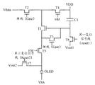
- FIG. 1a is a schematic diagram of a part of a pixel driving circuit provided by an embodiment of the disclosure
- FIG. 1b is a schematic diagram of a first basic structure of a display substrate provided by an embodiment of the disclosure
- FIG. 1c is a schematic structural diagram of a first conductive pattern provided by an embodiment of the disclosure.
- FIG. 2 is a schematic diagram of a first structure in a display area of a display substrate provided by an embodiment of the disclosure
- FIG. 3 is a schematic structural diagram of a pixel driving circuit provided by an embodiment of the disclosure.
- FIG. 4 is a schematic diagram of a second structure in a display area of a display substrate provided by an embodiment of the disclosure.
- Fig. 5 is a schematic cross-sectional view along the direction D1D2 in Fig. 4;
- FIG. 6 is a schematic structural diagram of a corner area in a display substrate provided by an embodiment of the disclosure.
- Fig. 7 is a schematic cross-sectional view taken along the direction E1E2 in Fig. 6;
- Figure 8 is a schematic diagram of the fourth metal process flow
- FIG. 9 is a schematic diagram of a third structure in the display area of the display substrate provided by an embodiment of the disclosure.
- FIG. 10 is a schematic diagram of a fourth structure in a display area of a display substrate provided by an embodiment of the present disclosure.
- 11a to 11e are the first flowcharts of the lift-off process at the M1M2 section in FIG. 2;
- FIG. 12a is a schematic diagram of a fifth structure in a display area of a display substrate provided by an embodiment of the disclosure.
- FIG. 12b is a schematic diagram of a sixth structure in the display area of the display substrate provided by an embodiment of the disclosure.
- FIG. 13a is a schematic diagram of a seventh structure in a display area of a display substrate provided by an embodiment of the disclosure.
- FIG. 13b is a schematic diagram of an eighth structure in a display area of a display substrate provided by an embodiment of the disclosure.
- FIG. 14a is a schematic diagram of a second basic structure of a display substrate provided by an embodiment of the disclosure.
- 14b is a schematic diagram of a fifth structure in the display area of the display substrate provided by an embodiment of the disclosure.
- Figure 14c is a schematic cross-sectional view along the F1F2 direction in Figure 14b;
- FIG. 15 is a schematic diagram of a sixth structure in a display area of a display substrate provided by an embodiment of the disclosure.
- Fig. 16 is a schematic cross-sectional view along the G1G2 direction in Fig. 15;
- FIG. 17 is a schematic structural diagram of a display substrate extending from a display area to a non-display area in a display substrate provided by an embodiment of the disclosure.
- FIG. 18 is a schematic cross-sectional view along the K1K2 direction in FIG. 17;
- 19 is a schematic diagram of the layout position of the auxiliary cathode layer and the second conductive connection pattern in the display area provided by an embodiment of the present disclosure
- FIG. 20 is a schematic diagram of a seventh structure in a display area of a display substrate provided by an embodiment of the present disclosure
- FIG. 21 is a schematic diagram of an eighth structure in a display area of a display substrate provided by an embodiment of the disclosure.
- Figures 22a to 22e are the second process diagrams of the lift-off process at the P1P2 section in Figure 21.
- the power consumption of the display device mainly includes the logic power consumption of the chip (IC) and the EL (Electroluminescence) power consumption.
- the EL power consumption P U ⁇ I.
- EL power consumption is mainly determined by the voltage difference between the positive power supply signal line VDD and the negative power supply signal line VSS.
- OLED Organic Light-Emitting Diode
- VDD is generally interconnected with the Gate2 pattern (made of the second gate metal layer) in the display panel to reduce the VDD voltage drop.
- the sheet resistance of the Gate2 pattern is 0.5 About ⁇ /sq.
- VSS is the edge wiring of the display panel.
- VSS is generally made of a metal layer of magnesium silver and surrounds the display area of the display panel.
- the voltage drop generated by the VSS is large, which is the main factor that affects the power consumption of the screen.
- the factors that cause the high power consumption of the display device include: the large voltage drop (IR-Drop) generated on the VSS in the display device; therefore, the ineffective voltage of the VSS can be reduced by reducing the IR-Drop generated on the VSS. Therefore, the voltage difference between VSS and VDD can be reduced, and the power consumption of the display device can be reduced.
- the large voltage drop (IR-Drop) generated on the VSS in the display device therefore, the ineffective voltage of the VSS can be reduced by reducing the IR-Drop generated on the VSS. Therefore, the voltage difference between VSS and VDD can be reduced, and the power consumption of the display device can be reduced.
- an embodiment of the present disclosure provides a display substrate, including: a display area and a non-display area located at the periphery of the display area, the display area includes a plurality of pixel opening areas and located at the The pixel spacer region between the pixel opening regions; the display substrate further includes: a first electrode 2, at least part of the first electrode 2 is located in the pixel spacer region, the first electrode 2 is on the display substrate The orthographic projection on the substrate and the orthographic projection of the pixel opening area on the substrate do not overlap; and, the second electrode 3 electrically connected to the first electrode 2, and the second electrode 3 is located in the Non-display area.
- the first electrode 2 is formed as a mesh structure.
- the display substrate may include a display area and a non-display area, wherein a plurality of repeating units are provided in the display area, each repeating unit includes a plurality of sub-pixels, and each sub-pixel includes a corresponding pixel opening area,
- the area located at the periphery of each pixel opening area forms a pixel spacer area.
- the orthographic projection of the pixel spacer region on the base of the display substrate and the projection of the pixel opening region on the substrate are adjacent to but not overlapping, and each pixel opening region and the pixel spacer region form a complete display area , For example, a rectangular area or a rounded rectangular area.
- the non-display area surrounds the display area.
- the non-display area includes four areas located above, below, left, and right of the display area.
- a fan-out line located in the fan-out area 72
- a test circuit 70 may be provided in an area below the display area in the non-display area.
- the left and right areas are respectively provided with gate drive circuits 75.
- the display area includes gate lines and data lines that are arranged crosswise, and both the gate lines and the data lines can be coupled to a driving chip through a corresponding fan-out line to receive a driving signal provided by the driving chip.
- the gate line and the data line may also be coupled to the test circuit through a corresponding fan-out line, and receive the test signal provided by the test circuit.
- the gate line and the data line may be electrically connected to a driving circuit formed on the display substrate, and further connected to a driving chip or a power supply.
- the specific structure of the first electrode 2 included in the display substrate is various.
- the first electrode 2 is formed as a mesh structure, and at least a part of the first electrode 2 can be located in pixels in the display area. In the spacer area, the orthographic projection of the first electrode 2 of the mesh structure on the substrate and the orthographic projection of each pixel opening area on the substrate do not overlap.
- the first electrode 2 shown in FIG. 1b is represented by a horizontal and vertical cross-shaped pattern, the first electrode 2 in FIG. 1b is actually formed as an integral structure, that is, the first electrode 2 included in the display substrate
- the electrode 2 is formed by a patterning process on the same layer of conductive material.
- the second electrode 3 electrically connected to the first electrode 2 may also be provided in the non-display area.
- the second electrode 3 may extend along the frame of the display substrate, the second electrode 3 surrounds the display area and can be electrically connected to a flexible circuit board in the display substrate, and the first electrode 2 can be electrically connected to the portions of the second electrode 3 located on the upper, lower, left, and right frames of the display substrate, respectively.
- the second electrode 3 is provided in the non-display area, the first electrode 2 of the mesh structure is provided in the pixel spacer area in the display area, and the display substrate is provided.
- the first electrode 2 and the second electrode 3 are electrically connected, so that when the first electrode 2 and the second electrode 3 are used together as the VSS in the display substrate, the resistance of the VSS can be greatly reduced Therefore, the voltage drop of the VSS is reduced, thereby reducing the voltage difference between the VSS and the power signal line VDD in the display substrate, and better reducing the power consumption of the display substrate. It is worth noting that according to the IR-Drop simulation results, the VSS voltage drop can be reduced by about 0.5V.
- the local heating phenomenon caused by the large current on the VSS is well improved.
- the width of the second electrode 3 located in the non-display area can be appropriately reduced, The width of the positive power signal line VDD included in the display substrate can be appropriately increased, so that the local heating phenomenon caused by the large current on VDD can be effectively improved.
- the first electrode 2 is disposed in the pixel spacer area, and the orthographic projection of the first electrode 2 on the base of the display substrate is different from the orthographic projection of the pixel opening area on the base. Therefore, the first electrode 2 will not affect the pixel aperture ratio of the display substrate.
- the display substrate further includes: a plurality of anode patterns 4 corresponding to the plurality of pixel opening regions one-to-one, and the orthographic projection of the pixel opening regions on the substrate It is located inside the orthographic projection of the corresponding anode pattern 4 on the substrate; the first electrode 2 and the anode pattern 4 are arranged in the same layer and the same material, and are insulated from the anode pattern 4.
- the display substrate includes a driving circuit layer
- the driving circuit layer includes a plurality of pixel driving circuits
- the specific structure of the pixel driving circuit can be set according to actual needs.
- the pixel driving circuit selects a 7T1C circuit, which includes 7 transistors and a capacitor.
- the 7T1C pixel circuit includes: a first transistor T1, a second transistor T2, a third transistor T3, The fourth transistor T4, the fifth transistor T5, the sixth transistor T6, the seventh transistor T7 and the first capacitor C1.
- the gate of the sixth transistor T6 is electrically connected to the first reset signal line reset1
- the first electrode of the sixth transistor T6 is electrically connected to the first initialization signal line Vinit1
- the second electrode of the sixth transistor T6 is electrically connected to The gate of the first transistor T1 is electrically connected.
- the gate of the third transistor T3 is electrically connected to the gate line gate, the first electrode of the third transistor T3 is electrically connected to the second electrode of the first transistor T1, and the second electrode of the third transistor T3 is electrically connected to the second electrode of the first transistor T1.
- the gate of a transistor T1 is electrically connected.
- the first electrode of the first transistor T1 is electrically connected to the second electrode of the second transistor T2
- the gate of the second transistor T2 is electrically connected to the gate line gate
- the second electrode of the second transistor T2 is electrically connected.
- One pole is electrically connected to the data line Vdata.
- the gate of the fourth transistor T4 is electrically connected to the light emission control signal line EM, the first electrode of the fourth transistor T4 is electrically connected to the positive power signal line VDD, and the second electrode of the fourth transistor T4 is electrically connected to the The first electrode of the first transistor T1 is electrically connected.
- the gate of the fifth transistor T5 is electrically connected to the light emission control signal line EM, the first electrode of the fifth transistor T5 is electrically connected to the second electrode of the first transistor T1, and the fifth transistor T5 The second pole of is electrically connected to the anode pattern 4 of the OLED in the corresponding sub-pixel.
- the gate of the seventh transistor T7 is electrically connected to the second reset signal line reset2, the first electrode of the seventh transistor T7 is electrically connected to the second initialization signal line Vinit2, and the second electrode of the seventh transistor T7 is electrically connected to The anode pattern 4 of the OLED in the corresponding sub-pixel is electrically connected. It should be noted that the timing of the second reset signal transmitted on the second reset signal line reset2 may be the same as or different from the timing of the scan signal transmitted on the gate line gate.
- the display substrate includes a plurality of repeating units, each repeating unit includes a plurality of sub-pixels, and the OLED in each sub-pixel includes anode patterns 4, organic Luminescent material layer and cathode.
- the anode pattern 4 is located on the side of the corresponding pixel driving circuit facing away from the substrate, and is electrically connected to the corresponding pixel driving circuit, and can receive the driving signal provided by the corresponding pixel driving circuit.
- the organic light-emitting material layer emits light under the action of the corresponding anode pattern 4 and the cathode.
- the display substrate may also include some spare sub-pixels (dummy sub-pixels) arranged at the periphery of the display area.
- dummy sub-pixels may include structures such as light-emitting layers and pixel openings according to actual needs, or may not include anode patterns and Structures such as pixel openings, or dummy sub-pixels can be set to have exactly the same structure as the sub-pixels included in the display area, but the dummy sub-pixels are not used for display. It can be seen that, in some cases, the anode patterns and pixel openings of these dummy sub-pixels may not correspond one-to-one.
- the specific layout of the anode pattern 4 is various.
- the orthographic projection of the pixel opening area on the substrate can be set to be located inside the corresponding orthographic projection of the anode pattern 4 on the substrate.
- it may specifically include: the orthographic projection of the anode pattern 4 on the base of the display substrate, and the orthographic projection of the pixel opening area surrounding its corresponding sub-pixel on the base.
- the first electrode 2 can be Set the same layer and the same material as the anode pattern 4, and arrange the first electrode 2 in the gap by setting a suitable electrode shape and width, so that the first electrode 2 is formed into a mesh structure as a whole, And make the orthographic projection of the first electrode 2 on the substrate and the orthographic projection of the anode pattern 4 on the substrate do not overlap, so as to ensure that there is a gap between the first electrode 2 and the anode pattern 4 insulation.
- the first electrode 2 and the anode pattern 4 are arranged in the same layer and the same material, so that the first electrode 2 and the anode pattern 4 can be patterned in the same time. It is formed at the same time, which greatly simplifies the manufacturing process of the display substrate and saves the manufacturing cost.
- the first electrode 2 and the anode pattern 4 are arranged in the same layer, so that the positive power signal line (VDD) in the display substrate has a larger layout space, so that a larger area of positive power signal can be laid out. Line to reduce the voltage drop generated on the positive power signal line.
- VDD positive power signal line
- both the anode pattern 4 and the first electrode 2 are made of indium tin oxide (ITO), silver (Ag), oxide Indium tin (ITO) laminated structure.
- ITO indium tin oxide
- Ag silver
- ITO oxide Indium tin
- the second electrode 3 and the first electrode 2 may be arranged in the same layer and the same material.
- the first electrode 2 and the second electrode 3 when the first electrode 2 and the second electrode 3 are laid out, the first electrode 2 and the second electrode 3 can be arranged in the same layer and the same material, so that the first electrode 2 and the second electrode 3 are arranged in the same layer and the same material.
- the second electrode 3 can be formed at the same time in a patterning process, and the first electrode 2 and the second electrode 3 can be directly electrically connected during production, without the need to add an additional via process, and the process is feasible High sex.
- first electrode 2, the second electrode 3 and the anode pattern 4 can be arranged in the same layer and the same material, so that the first electrode 2, the second electrode 3 and the anode
- the patterns 4 can all be formed in the same patterning process, which simplifies the manufacturing process of the display substrate and saves the manufacturing cost of the display substrate.
- the second electrode 3 may include a first conductive pattern 31 and a second conductive pattern 32 that are stacked, and the first conductive pattern 31 is located on the base of the display substrate.
- the first conductive pattern 31 includes: a ring portion 310, a first wire inlet portion 311, and a second wire portion 312;
- the ring portion 310 surrounds the display area, and There is an opening, and the opening of the ring portion 310 has a first end and a second end;
- the first inlet portion 311 is electrically connected to the first end;
- the second inlet portion 312 is electrically connected to the second end Portion is electrically connected;
- the second conductive pattern 32 is in a ring shape, the orthographic projection of the second conductive pattern 32 on the base of the display substrate and the orthographic projection of the ring portion 310 on the base have a first Overlapping area.
- the second conductive pattern 32 is electrically connected to the ring portion;
- the first conductive pattern 31 may be made of a source-drain metal layer, that is, made of the same layer and the same material as the first electrode and the second electrode of each transistor in the pixel driving circuit.
- the first conductive pattern 31 can be made of the same layer and the same material as the source and drain metal layers.
- the first conductive pattern 31 can be made of the same layer and the same material as the first source/drain metal layer or the second source/drain metal layer.
- the second conductive pattern 32 can be made of the same layer and the same material as the first electrode 2. Further, the second conductive pattern 32 can be made of the same layer and the same material as the first electrode 2 and the anode pattern 4.
- the specific shapes of the first conductive pattern 31 are various.
- the first conductive pattern 31 includes the ring portion 310 (as shown in FIG. 6 with H2 width), the first wire entry portion 311 and the second wire entry portion 312, the ring portion 310 surrounds the display area, and the opening of the ring portion 310 faces the binding of the driving chip in the display substrate Set location.
- the display area is approximately a rectangular area, and the opening of the ring portion 310 and the binding position of the driving chip in the display substrate are located on the same side of the display area, for example, the rectangular area.
- the first wire inlet 311 and the second wire inlet 312 may be electrically connected to the flexible circuit board for receiving signals provided by the flexible circuit board.
- annular portion 310, the first wire inlet portion 311, and the second wire inlet portion 312 may be formed as an integral structure, but are not limited to this.
- the specific shapes of the second conductive pattern 32 are various.
- the second conductive pattern 32 has a ring shape (as shown in FIG. 6 with a width of H1).
- the second conductive pattern 32 includes two sub-graphics arranged oppositely, one of the sub-graphics is located on the left side of the display area, and the other sub-graphic is located on the right side of the display area.
- the second conductive pattern 32 may be U-shaped, that is, the second conductive pattern 32 includes parts located on the left, right, and lower sides of the display area.
- the width H1 and the width H2 in FIG. 6 only exemplarily show the width of the ring portion 310 and the second conductive pattern 32 on the display panel.
- the ring portion 310 and the second conductive pattern 32 The conductive pattern 32 can be set to have the same width or different widths at different positions of the display panel, and the width refers to the width along the extending direction perpendicular to itself.
- the part of the ring part 310 on the left side and the part on the right side of the display panel can be set to have the same width, and the part of the ring part 310 on the upper side and the lower side of the display panel can also be set to have the same width;
- the two conductive patterns 32 can also be arranged in the same way, which will not be repeated here.
- the orthographic projection of the second conductive pattern 32 on the substrate and the orthographic projection of the annular portion 310 on the substrate may be provided in the first overlapping area .
- the orthographic projection of the first overlapping area on the substrate is a ring with an opening, and the first overlapping area can be covered by a portion of the ring portion 310 that does not overlap the second conductive pattern 32 Surrounded by an orthographic projection on the substrate.
- the second conductive pattern 32 also includes a portion that does not overlap the ring portion 310.
- the orthographic projection of the portion on the substrate a part of it can be covered by the first intersection.
- the overlapping area is surrounded by the orthographic projection on the substrate, and the other part is located at the opening of the orthographic projection of the first overlapping area on the substrate.
- the specific electrical connection manners of the second conductive pattern 32 and the ring portion 310 are various.
- the second conductive pattern 32 is electrically connected to the ring portion 310 through the first via hole.
- the orthographic projection of the first via hole on the substrate may be a ring shape with an opening, and the ring shape opening overlaps the opening of the ring portion 310
- the extension direction of other parts of the ring is substantially the same as the extension direction of the ring portion 310.
- X1 represents the width of this portion perpendicular to its extending direction. It should be noted that the width of the ring-shaped first via in the direction perpendicular to its own extension can be set according to actual needs, and the width can be the same or different in different parts of the ring-shaped first via.
- the first via may also be configured to include a plurality of sub-vias independent of each other, and the specific distribution modes of the plurality of sub-vias are various.
- the plurality of sub-vias are evenly distributed in the first overlapping area; or the plurality of sub-vias are sequentially spaced along the extension direction of the first overlapping area; or the plurality of sub-vias It is divided into multiple groups of sub-vias, and the multiple groups of sub-vias are correspondingly distributed at different positions of the first overlapping area.
- the size of the plurality of sub-vias can be set according to actual needs, as long as the orthographic projections of the plurality of sub-vias on the substrate are located in the first overlapping area.
- the annular portion 310 and the second conductive pattern 32 are arranged in different layers, and an insulating layer is arranged between the annular portion 310 and the second conductive pattern 32.
- the insulating layer includes a flat layer 81, and the first via X1 is formed on the flat layer 81 and penetrates the flat layer 81.
- the following solution is also included: located at the first conductive pattern 31 and the second conductive pattern 31 In the insulating layer between the two conductive patterns 32, the part where the orthographic projection on the substrate can overlap with the first overlapping area is removed, and the second conductive pattern in the groove is located on the first conductive pattern 31
- the ring portion 310 faces away from the surface of the substrate and is completely attached to the surface of the ring portion 310 away from the substrate.
- connection modes of the first electrode 2 and the second conductive pattern 32 are various.
- the first electrode 2 and the ring-shaped second conductive pattern 32 are connected in multiple directions, as shown in FIG. 1b, FIG. 6 and FIG. 7, and the first electrode 2 includes FIGS. 6 and
- the X4 part located in the non-display area in FIG. 7 can be connected to the ring-shaped second conductive pattern 32 in four directions: up, down, left, and right. It is worth noting that the direction from left to right in FIG. 7 is the direction from the non-display area to the display area.
- the direct electrical connection between the first electrode 2 and the second conductive pattern 32 includes: the first electrode 2 and the second conductive pattern 32 are an integral structure; or the first electrode 2 is separated from the display area Extend to the non-display area, and continue to extend away from the display area to form a ring-shaped second conductive pattern 32; Two conductive patterns 32.
- the second electrode 3 includes the first conductive pattern 31 and the second conductive pattern 32, and the second conductive pattern 32 and the first electrode 2 are in the same layer.
- the same material settings can achieve the following technical effects:
- the second conductive pattern 32 can be formed in the same patterning process as the first electrode 2, and at the junction of the first electrode 2 and the second conductive pattern 32, the first electrode 2 and The second conductive pattern 32 can realize a direct electrical connection, and no additional via design is required, that is, no cross-line-transfer layer is required.
- the manufacturing process flow of the display substrate may include: in a direction away from the substrate, on the substrate substrate (which may include a first polyimide layer, a first barrier layer, and a second layer that are stacked in sequence).
- the two polyimide layer and the second barrier layer are sequentially formed on the layered buffer layer Buffer, barrier layer Barrier, active layer Active, first insulating layer GI1, first gate metal layer Gate1, second insulating layer GI2, The second gate metal layer Gate2, the third insulating layer ILD, the source and drain metal layer SD, the planarization layer 81 (PLN), the anode layer Anode, the pixel defining layer 80 (PDL) and the spacer 82 (ie PS) layer, wherein The first gate metal layer Gate1, the second gate metal layer Gate2, the source/drain metal layer SD and the anode layer Anode are all conductive layers made of at least one of metal, alloy or metal oxide, namely 4-step patterning process.
- the first electrode 2 is electrically connected to the ring-shaped second conductive pattern 32 from multiple directions, so that the current on the second electrode 3 is no longer solely on the display substrate.
- the fixed position of the PNL such as the corner 33 of the display substrate, flows into the chip of the display substrate, but is dispersed into the grid-shaped first electrode 2, the ring-shaped second conductive pattern 32 and the first conductive pattern 31 Therefore, the problem of local heating generated at the corner 33 of the display substrate is well improved.
- the first electrode 2 and the second electrode 3 are applied to VSS signal transmission, the current on the VSS trace in the peripheral area is reduced, and the excessive current on the VSS trace near the chip is improved. The resulting heat problem.
- the first electrode 2 further includes a portion (X4 in FIG. 6) located in the non-display area, which is electrically connected to the second electrode 3 and also That is, the first electrode 2 is electrically connected to the second electrode 3 through this portion.
- the first electrode 2 has a mesh structure, the display area of the mesh structure is partially located in the pixel interval of the display area, and the non-display area of the mesh structure is located in the non-display area.
- the display area portion may be extended from the display area portion located in the pixel spacing area, that is, the non-display area portion and the display area portion located in the pixel spacing area are formed as an integral structure.
- the wiring pattern of the non-display area portion may be consistent with the wiring pattern of the display area portion, for example, the wiring pattern of the non-display area portion located in the middle area of each side of the display area, and the display area portion directly connected to it.
- the shape of the trace pattern is roughly the same.
- the wiring pattern of the non-display area portion may be inconsistent with the wiring pattern of the display area portion, for example, it is located at each corner of the display area, and each wiring pattern may be reasonably distributed according to the distance between the wiring lines and the size of the space.
- the direction of the line pattern for example, try to be evenly distributed, the zigzag pattern and the direction of the line are roughly the same, and the spacing between the lines is roughly the same.
- the pattern of the part connected to the second electrode 3 and The way can be the same.
- the same intersects the part of the second electrode 3 close to the side of the display area.
- the part where the non-display area part is connected to the second electrode 3 is perpendicular or parallel.
- the above-mentioned arrangement of the first electrode 2 also includes a part located in the non-display area, and is electrically connected to the second electrode 3 through this part, so that the first electrode 2 can be connected to the second electrode 3 through a plurality of branches.
- the two electrodes 3 are connected, which is more conducive to the dispersion of current on the second electrode 3 and more effectively improves the heat dissipation problem of the second electrode 3.
- the display substrate further includes:
- the third electrode 5 is electrically connected to the first electrode 2.
- the third electrode 5 includes a first part, a second part, and a third part.
- the first part is inside the orthographic projection on the substrate, the second part is located in the pixel spacer area, and the third part is located in the non-display area.
- the display substrate may further include a third electrode 5.
- the third electrode 5 is a cathode in the display substrate, and the cathode is located on the side of the first electrode 2 facing away from the substrate. One side.
- first part, the second part, and the third part may be formed as an integral structure, that is, as a whole layer; or may be electrically connected to each other through a conductive connection part, the third electrode
- the area of 5 is larger than the area of the display area.
- X2 in FIG. 6 represents the boundary of the third electrode 5.
- connection position between the non-display area part of the mesh structure and the third electrode 5 is approximately evenly distributed along the boundary of the display area (except the side where the IC is bound) to ensure that the contact resistance of each position is approximately equal , To ensure the uniformity of the signal.
- connection positions of the non-display area portion and the third electrode 5 are roughly evenly distributed along two opposite sides of the display area that are adjacent to one side where the IC is bound.
- the dummy sub-pixels may not be covered by the third electrode 5, but it is not limited to this.
- the light-emitting side electrode of the display substrate is a cathode, which is generally a Mg/Ag alloy.
- the Mg/Ag metal is made very thin; on the other hand, the negative power signal line (VSS) electrically connected to the cathode in the related art is only a trace located at the edge of the display substrate. Therefore, the resistance of the cathode is relatively large (when the cathode is made of Mg/Ag alloy, the square resistance of the cathode is between 10 ⁇ /sq ⁇ 15 ⁇ /sq).
- the IR drop problem caused by the cathode leads to uneven display of the display substrate and the display substrate The power consumption becomes larger.
- the orthographic projection of the second part of the third electrode 5 on the substrate can be set to be in line with the first electrode 2
- the orthographic projection on the substrate has a second overlapping area, and the second part of the third electrode 5 is electrically connected to the first electrode 2 through a second via 84 provided in the second overlapping area.
- the third part of the electrode 5 is electrically connected to the second conductive pattern 32 through a third via hole (via X3 in FIG. 6) provided in the third overlapping area.
- the second via hole 84 penetrates the pixel defining layer 80 located in the pixel interval, or the pixel defining layer 80 and the organic light emitting material layer 83, and the third via hole penetrates the pixel defining layer located in the non-display area. 80.
- the specific positions, number and size of the second via 84 and the third via can be set according to actual needs, for example, according to the structure of the pixel defining layer, the spatial layout of the first electrode, contact resistance, and aperture ratio And other factors to design.
- the orthographic projection of the third via on the substrate may be ring-shaped; or the third via includes a plurality of independent sub-vias, and these independent sub-vias are distributed at intervals in the The third overlap area.
- the lift-off process (a lift-off process) can be used to fabricate the second via hole 84, and the specific process steps are as follows:
- the anode pattern 4 and the first electrode 2 are formed on the side of the driver circuit layer facing away from the substrate, and then the pixel defining layer 80 and the spacer are formed. ⁇ 82.
- the driving circuit layer 85 refers to a structure that realizes the driving circuit shown in FIG. 3, and may include an active layer, a gate insulating layer, a gate metal layer, an interlayer insulating layer, a source-drain metal layer, and other structures.
- the pixel defining layer 80 is generally a mesh structure, in which a plurality of first openings 86 and a pixel isolation structure (located in the pixel spacer area) surrounding the plurality of first openings 86 are formed, and a plurality of second via holes 84 and A plurality of third via holes (via X3 in FIG. 6) are formed in the pixel isolation structure.
- the first opening 86 corresponds to the anode pattern 4 one-to-one
- the pixel isolation structure covers the edge of the anode pattern 4, and the first opening 86 can expose the corresponding anode pattern 4 At least partly.
- the first electrode 2 can be arranged in the same layer and the same material as the anode pattern 4.
- the first electrode 2 is located on the side of the pixel isolation structure close to the substrate.
- the pixel isolation structure covers the first electrode 2 and the second via 84 in the pixel isolation structure can expose a part of the first electrode 2.
- the second conductive pattern 32 can be arranged in the same layer and the same material as the anode pattern 4.
- the second conductive pattern 32 is located on the side of the pixel isolation structure close to the substrate, and the third via hole can expose a part of the second conductive pattern 32 in the second electrode 3.
- the spacer 82 and the pixel defining layer 80 can be formed at the same time in a patterning process. Specifically, a halftone mask can be used.
- a sacrificial material layer is deposited on the substrate on which the spacer 82 is formed, a photoresist is formed on the surface of the sacrificial material layer facing away from the substrate, and a sacrificial pattern located in the second via 84 is formed through processes such as exposure, development, and etching.
- the process flow of making the sacrificial layer 9 is as follows: an organic material is used to form a sacrificial material layer, a negative photoresist layer is formed on the side of the sacrificial material layer facing away from the substrate, and the negative photoresist layer is formed using a mask.
- the photoresist layer is exposed to form a negative photoresist retention area and a negative photoresist removal area.
- the negative photoresist retention area corresponds to the area where the sacrificial pattern 9 is located, and the negative photoresist
- the resist removal area corresponds to other areas except the area where the sacrificial pattern 9 is located, the negative photoresist layer located in the negative photoresist removal area is removed, and the remaining negative photoresist layer is used as a mask,
- the sacrificial material layer is wet-etched to form the sacrificial pattern 9 with an inverted trapezoidal cross-section.
- the film layer immediately below the sacrificial pattern 9 should be as flat as possible, which is more conducive to the stripping process.
- the specific formation position of the sacrificial pattern 9 is related to the contact position between the first electrode 1 and the third electrode 5, that is, the specific formation position of the sacrificial pattern 9 is related to the second via 84
- the sacrificial pattern 9 is located in the pixel interval area
- the sacrificial pattern 9 is located in the non-display area. Display area.
- the sacrificial pattern 9 is formed in the second via 84.
- the vapor deposition is continued to form an organic light-emitting material layer 83.
- the organic light-emitting material layer 83 may cover the portion of the anode pattern 4 exposed by the first opening 86, or cover the second via 84 and the spacer 82.
- the organic light-emitting material layer 83 also includes a fourth portion and a fifth portion, the fourth portion covering the pixel isolation structure and a portion of the first electrode 2 exposed by the second via hole 84, and the fifth portion covering the pixel isolation structure.
- the sacrificial pattern 9 in the second via 84, the fourth part and the fifth part are disconnected at the edge of the sacrificial pattern 9 in the second via 84, so that the fourth part and the The fifth part is independent of each other.
- the organic light-emitting material layer 83 of the above structure can emit white light, and in this case, as shown in FIG. 11c and FIG. Resistance pattern R, green color resistance pattern G, blue color resistance pattern B, etc.). Moreover, when the white organic light-emitting material layer 83 is formed, the white organic light-emitting material layer 83 may be formed on both the upper and lower layers of the color group pattern. In addition, it is also possible to form a colored organic light-emitting material layer only in the first opening 86, for example, a red organic light-emitting material layer is formed in some of the first openings, and a green organic light-emitting material layer is formed in other first openings. A blue organic light-emitting material layer is formed in the remaining first openings.
- the substrate on which the organic light-emitting material layer 83 is formed is immersed in a peeling solution, and then taken out after standing for 0.5 min to 2 min, and then the substrate is appropriately tilted to facilitate the sacrificial pattern 9 to fall off.
- the photoresist on the sacrificial surface and the fifth part of the organic light-emitting material layer 83 are simultaneously taken away.
- the stripping liquid can be a fluoroether solvent that can dissolve the material of the sacrificial layer and does not damage the organic light-emitting material layer 83.
- the third electrode 5 is continuously evaporated, and the first part of the third electrode 5 covers the plurality of pixel opening regions (that is, the first opening 86).
- the second part of the third electrode 5 is located in the pixel spacer area and can be electrically connected to the first electrode 2 through the second via hole 84, and the third part of the third electrode 5 can pass through the third The via hole is connected to the second conductive pattern 32 of the second electrode 3.
- the first electrode 2 is the metal film closest to the cathode. In the process, the interconnection between the first electrode 2 and the cathode is less difficult to achieve.
- the gap space between the anode patterns 4 or the position of the anode pattern 4 are used to realize the rational layout of the first electrode 2 and interconnect with the upper cathode, which is equivalent to introducing and An auxiliary electrode connected in parallel with the cathode can effectively reduce the resistance of the cathode, thereby improving the IR drop problem of the cathode.
- the VSS is The current path is changed from two-dimensional to three-dimensional distribution, that is, the VSS current can not only converge from the cathode to the periphery to the second electrode 3, and then flow into the chip, but also can converge to the chip through the first electrode 2, that is, the display area
- the internal cathode current has two layers of current paths.
- the third portion of the third electrode 5 is electrically connected to the second conductive pattern 32 of the second electrode 3 through the third via hole provided in the third overlapping area, the third electrode 5 is not connected to the second conductive pattern 32 in the display area.
- the overlapping area of the second electrode 3 can be completely compatible with the manufacturing process in the related technology, and no additional process flow is required.
- the resolution of the display substrate is Full High Definition (FHD) level, and the pixels are arranged in a GGRB manner.
- FHD Full High Definition
- the VSS resistance is reduced by about 40%.
- the layout of the first anode is shown in FIG. 9, FIG. 11a and FIG.
- the trace width of the first electrode 2 can be about 4 ⁇ m, and the distance from the anode pattern 4 is at least 3 ⁇ m (depending on the process capability).
- the perforated area where the first electrode 2 is connected to the cathode avoids the anode pattern 4 and the spacer 82.
- the position of the perforated area is determined according to the gap between adjacent anode patterns 4.
- the perforated area is evenly distributed.
- the size of the first electrode 2 exposed by the second via hole 84 in the perforated area may be 11 ⁇ m ⁇ 11 ⁇ m.
- the orthographic projection of the second via 84 on the substrate may be located inside the orthographic projection of the first electrode 2 on the substrate.
- the orthographic projection of the first opening 86 of the pixel defining layer 80 on the substrate may be located inside the orthographic projection of the corresponding anode pattern 4 on the substrate, and the area of the orthographic projection of the first opening 86 on the substrate It is smaller than the area of the orthographic projection of the corresponding anode pattern 4 on the substrate.
- the minimum distance between the boundary of the orthographic projection of the second via 84 on the substrate and the boundary of the orthographic projection of the first electrode 2 on the substrate is at least 1.5 ⁇ m.
- the sacrificial pattern 9 is located inside the second via 84 of the pixel defining layer 80, and the orthographic projection of the sacrificial pattern 9 on the substrate is corresponding to the orthographic projection of the second via 84 on the substrate.
- the projection surrounds, and the minimum distance between the boundary of the orthographic projection of the first sacrificial pattern 9 on the substrate and the boundary of the orthographic projection of the second via 84 on the substrate is at least 1.5 ⁇ m.
- the resolution of the display substrate is at the FHD level, and the pixels are arranged in a strip (strip) manner.
- the VSS resistance is reduced by about 40%.
- the layout of the first anode is shown in FIG. 10, the first electrode 2 avoids the anode pattern 4, and is interconnected to form a mesh structure in the entire display area.
- the trace width of the first electrode 2 can be selected to be about 3 ⁇ m, and the distance from the anode pattern 4 is at least 3 ⁇ m (depending on the process capability).
- the perforated area where the first electrode 2 overlaps with the cathode that is, the second via 84) avoids the anode pattern 4 and the spacer 82.
- the position of the perforated area is determined according to the gap between adjacent anode patterns 4, as far as possible
- the first electrodes 2 are evenly distributed.
- the size of the first electrode 2 exposed by the second via hole 84 in the perforated area may be 11 ⁇ m ⁇ 11 ⁇ m.
- the orthographic projection of the second via 84 on the substrate may be located inside the orthographic projection of the first electrode 2 on the substrate.
- the orthographic projection of the first opening 86 of the pixel defining layer 80 on the substrate may be located inside the orthographic projection of the corresponding anode pattern 4 on the substrate, and the area of the orthographic projection of the first opening 86 on the substrate Smaller than the area of the orthographic projection of the corresponding anode pattern 4 on the substrate, the boundary of the orthographic projection of the second via 84 on the substrate, and the boundary of the orthographic projection of the first electrode 2 on the substrate The minimum distance between them is at least 1.5 ⁇ m.
- the sacrificial pattern 9 is located inside the second via 84 of the pixel defining layer 80, and the orthographic projection of the first sacrificial pattern 9 on the substrate is formed on the substrate by the corresponding second via 84 Surrounded by the orthographic projection of the first sacrificial pattern 9 on the substrate, the minimum distance between the boundary of the orthographic projection of the first sacrificial pattern 9 on the substrate and the boundary of the orthographic projection of the second via 84 on the substrate is at least 1.5 ⁇ m .
- the second electrode 3 includes a negative power supply signal line (VSS) surrounding the display area, and the third electrode 5 includes a cathode.
- the second electrode 3 includes a reference signal line in the display substrate.
- the display substrate further includes: a plurality of repeating units, each repeating unit includes at least three sub-pixels arranged at intervals, and each sub-pixel includes a pixel opening area located between adjacent pixel opening areas. The area between the two forms the pixel spacer area.
- the display substrate may include a plurality of repeating units, the plurality of repeating units are arranged in an array, each repeating unit may include at least three sub-pixels arranged at intervals, and each of the sub-pixels included in the repeating unit It includes an organic light-emitting material layer 83, which can emit white light or colored light. When white light is emitted, each sub-pixel needs to be provided with a corresponding color resist pattern.
- the specific structures of the first electrode 2 are various. As shown in FIG. 10, in some embodiments, the first electrode 2 of the mesh structure may include a mesh body that defines a plurality of The first enclosed area 21 corresponds to the repeating unit one-to-one.
- the orthographic projection of the first enclosed area 21 on the base of the display substrate covers the corresponding repeating unit.
- An orthographic projection of an opening area on the substrate, and the opening area includes a pixel opening area included in each sub-pixel in the repeating unit.
- the orthographic projection of the first electrode 2 forming a closed area 21 on the substrate surrounds the orthographic projection of the opening area in the repeating unit located in the closed area 21 on the substrate.
- the grid body can define a plurality of first enclosed areas 21.
- the first enclosed area 21 means that the main body of the grid in the grid structure includes a plurality of line segments, which are connected end to end to the enclosed area, and there is no break in the area.
- the mesh structure includes a mesh body that defines a plurality of second enclosed areas 22; all of the plurality of repeating units includes The sub-pixels can be divided into multiple sub-pixel groups, and each group of sub-pixel groups includes at least one of the sub-pixels; the orthographic projection of the second enclosed area 22 on the base of the display substrate encloses the sub-pixels in a one-to-one correspondence The orthographic projection of the group on the substrate.
- the grid body can define a plurality of second enclosed areas 22, and the orthographic projection of the second enclosed areas 22 on the base of the display substrate encloses the sub-pixel groups in the one-to-one correspondence. Orthographic projection on the substrate.
- each sub-pixel group may include at least one sub-pixel, and each sub-pixel can only belong to one sub-pixel group.
- the grid body may be specifically located directly under the pixel defining layer 80 and covered by the pixel defining layer 80.
- the sub-pixel group may include at least one sub-pixel of the same color; and/or, the sub-pixel group may include at least two sub-pixels of different colors.
- each repeating unit includes one red sub-pixel, one blue sub-pixel, and two green sub-pixels;
- the orthographic projection of at least part of the grid body on the substrate is located between the orthographic projections of the first openings of the two green sub-pixels on the substrate.
- the minimum distance between the anode patterns 4 corresponding to adjacent green sub-pixels is generally about 15 ⁇ m. Therefore, at least part of the grid body can be set to be square on the substrate.
- the projection is located between the orthographic projections of the two green sub-pixels on the substrate, and the width of the grid body in the direction perpendicular to its own extension direction is set to be about 5 ⁇ m, which can ensure that the The good shunting effect of the first electrode 2 can also prevent a short circuit between the first electrode 2 and the anode pattern 4.
- the multiple repeating units are arranged in an array.
- the two green sub-pixels are arranged along a first direction, and the red sub-pixels are located at all the repeating units.
- the first side of the two green sub-pixels, the blue sub-pixel is located on the second side of the two green sub-pixels, the first side and the second side are opposite in a second direction, the first The two directions are perpendicular to the first direction.
- the first direction includes the Y direction
- the second direction includes the X direction.
- the repeating unit adopts the above structure, it is formed as a GGRB pixel arrangement.
- the anode connection via 1 corresponding to the blue sub-pixel can be specifically arranged between the anode connection via 1 corresponding to the adjacent green sub-pixel, and there is no
- the first electrode 2 is not limited to this.
- anode connection holes corresponding to each anode pattern 4 included in the display substrate are all arranged in a row and column direction, and the via holes in the same row are approximately in a straight line, and the spacing is approximately equal.
- green sub-pixels 103 are arranged in pairs adjacent to each other; a red sub-pixel 101 and a blue sub-pixel are arranged between two pairs of green sub-pixels 103 that are arbitrarily close. 102.
- all the green sub-pixels 103 in the first direction are paired as a pair, and the green sub-pixels 103 in each pair are arranged adjacent to each other.
- a red sub-pixel 101 and a blue sub-pixel 102 between two pairs of green sub-pixels 103 that are arbitrarily close are arranged oppositely in the second direction.
- the red sub-pixel 101 and the blue sub-pixel 102 are both arranged between two pairs of adjacent green sub-pixels 103, the requirement that the sub-pixel density is 1.5 times the pixel density can be satisfied.
- the ratio of the numbers of the red sub-pixels 101, the green sub-pixels 103, and the blue sub-pixels 102 is 1:2:1.
- the green sub-pixels 103 are arranged in pairs adjacent to each other; a red sub-pixel 101 and a blue sub-pixel 102 are arranged between two pairs of green sub-pixels 103 that are arbitrarily close.
- the sub-pixel density is 1.5 times the pixel density and the virtual pixel array is evenly distributed.
- green sub-pixels arranged in pairs adjacent to each other form a plurality of green sub-pixel pairs arranged in the second direction.
- two green sub-pixels in each pair of green sub-pixels are arranged along the first direction.
- all the green sub-pixels 103 located in the second direction are arranged in pairs as a pair adjacent to each other.
- the center of each pair can be The color layers of the two green sub-pixels 103 are connected together, and the green light-emitting layers of the two green sub-pixels 103 in each pair are formed through an evaporation hole of the FMM, thereby reducing the color of the green sub-pixel 103 to a certain extent. Difficulty of layer process.
- the adjacent green sub-pixels 103 can be arranged side by side in the first direction, and the position of the green sub-pixels 103 can be fine-tuned to realize the uniform distribution of the virtual pixel array, and the two nearest neighbors A certain distance is set between the green sub-pixels 103, which reduces the difficulty of the process and ensures the smoothness and continuity of the horizontal and vertical lines in the center of the bright spot to the greatest extent in the case of high resolution (as shown by the dashed lines in Figure 13a and Figure 13b). Show).
- the shapes of the red sub-pixel 101 and the blue sub-pixel 102 are both hexagons, and the three opposite sides of the hexagon are all parallel.
- each green sub-pixel 103 is a pentagon.
- the pentagon includes a set of parallel opposite sides and a vertical side, and the vertical side is perpendicular to the set of parallel opposite sides; wherein, in each pair of green sub-pixels 103 The vertical sides of the are arranged next to each other.
- a set of longer parallel opposite sides in the red sub-pixel 101 and a set of longer parallel opposite sides in the blue sub-pixel 102 are parallel to a set of parallel opposite sides in the green sub-pixel 103.
- the positions of the red sub-pixel 101, the blue sub-pixel 102, and the green sub-pixel 103 in each repeating unit can be adjusted arbitrarily, as long as the sub-pixel density is in the first direction and the second direction of the pixel array. Just 1.5 times the pixel density. For example, it can be as shown in Fig. 13a or as shown in Fig. 13b.
- each FMM can be designed to be close to a regular hexagon, which is conducive to FMM design; on the other hand, when the FMM evaporation process is used to evaporate sub-pixels, the FMM netting force can be mainly applied to the long side. Therefore, damage to the FMM can be avoided, which is beneficial to ensure the yield rate of the network.
- the red and blue sub-pixels in each repeating unit group are arranged along the second direction, and a pair of green sub-pixels are arranged along the first direction.
- the pair of red and blue sub-pixels and the green sub-pixel may be arranged along the second direction, or the pair of green sub-pixels may be arranged between one red sub-pixel and one blue sub-pixel.
- a plurality of repeating units are arranged along the second direction to form a repeating unit group (row).
- the dotted line along the second direction in the figure represents, for example, the center line of the repeating unit group.
- the multiple repeating unit groups are arranged along the first direction, thereby forming the entire pixel arrangement structure.
- adjacent repeating unit groups are staggered from each other in the second direction, that is, adjacent repeating unit groups have a certain offset along the second direction. Therefore, adjacent repeating units The sub-pixels of the same color in the group are not aligned in the first direction.
- the offset of the adjacent repeating unit group in the second direction is half of the size of the repeating unit in the second direction.
- the size of the repeating unit in the second direction is the pitch of the repeating unit in the second direction.
- the arrangement of pixels in the odd-numbered row repeating unit group is the same, and the pixels in the even-numbered row repeating unit group are arranged in the same manner.
- the center line of two green sub-pixels in each repeating unit is located between the centers of two adjacent red and blue sub-pixels in adjacent repeating units.
- the edges of the two green sub-pixels are inside the outer edges of the two adjacent red and blue sub-pixels, and the outer edge here refers to the edges of the two sub-pixels opposite to each other in the second direction. That is, the extension range of one green sub-pixel pair in the second direction is not greater than the extension range of the two adjacent red and blue sub-pixels in the second direction.
- the ratio of the number of pixels of red, blue, and green is 1:1:2.
- One red and one green sub-pixel constitute one pixel
- one blue and one green sub-pixel constitute one pixel.
- the embodiments of the present disclosure have no specific limitations on specific combinations. For example, one red-green sub-pixel and one green sub-pixel in a repeating unit form one pixel, and one blue sub-pixel and another green sub-pixel form another pixel. Or, for a pair of green sub-pixels in the same repeating unit, one of the green sub-pixels and one red sub-pixel in the repeating unit form a pixel, and the other green sub-pixel is connected to a blue sub-pixel in the adjacent repeating unit.
- the color sub-pixels form one pixel.
- the green sub-pixels are arranged in a first direction, and the sizes of the red and blue sub-pixels in the first direction are larger than their sizes in the second direction.
- the size of the red and blue sub-pixels in the first direction is larger than the size of the blue sub-pixels in the second direction.
- each repeating unit includes a red sub-pixel, a blue sub-pixel, and a green sub-pixel; the plurality of repeating units are arranged in an array, and the plurality of repeating units It can be divided into multiple columns of repeating units, each column of repeating units includes a plurality of repeating units arranged in a first direction (such as Y direction), and each column of repeating units can be divided into two columns of sub-pixels, and one column of sub-pixels includes a plurality of sub-pixels.
- the red sub-pixels and the plurality of blue sub-pixels, the red sub-pixels and the blue sub-pixels are alternately arranged along the first direction, and the other column of sub-pixels includes a plurality of green sub-pixels arranged along the first direction Pixels.
- the repeating unit when it adopts the above structure, it is formed into a strip-shaped pixel arrangement.
- the area of the body electrode of a green sub-pixel anode pattern is larger than the area of the body electrode of a blue sub-pixel anode pattern, and is larger than the area of the body electrode of a red sub-pixel anode pattern.
- the area of the body electrode of a red sub-pixel anode pattern is larger than the area of the body electrode of a blue sub-pixel anode pattern.
- the size of the body electrode of a green sub-pixel anode pattern in the Y direction is larger than the size of the body electrode of a blue sub-pixel anode pattern in the Y direction, and larger than the size of the body electrode of a red sub-pixel anode pattern in the Y direction .
- the size of the body electrode of a green sub-pixel anode pattern in the Y direction does not exceed the span of the body electrode of a blue sub-pixel anode pattern and the body electrode of a red sub-pixel anode pattern in the Y direction, that is, the green sub-pixel anode pattern
- the body electrode of the blue sub-pixel anode pattern, the body electrode of the red sub-pixel anode pattern and the body electrode of the red sub-pixel anode pattern are respectively projected on a straight line along the Y direction, the projection of the body electrode of the green sub-pixel anode pattern is located on the blue sub-pixel anode pattern Between the two most distant points of the projection of the main electrode of the red sub-pixel anode pattern and the main electrode of the red sub-pixel anode pattern.
- the size of the main electrode of a green sub-pixel anode pattern in the X direction, the size of the main electrode of the blue sub-pixel anode pattern in the X direction, and the size of the main electrode of the red sub-pixel anode pattern in the X direction are approximately the same.
- the size of the body electrode of the blue sub-pixel anode pattern in the X direction and the size of the body electrode of the red sub-pixel anode pattern in the X direction are approximately the same, and are approximately equal to the size of the body electrode of a green sub-pixel anode pattern in the X direction.
- the ratio is 0.8 to 1.2.
- connection electrode of the anode pattern of the blue sub-pixel, the connection electrode of the anode pattern of the red sub-pixel, and the connection electrode of the green sub-pixel are located on a straight line parallel to the X direction.
- the connecting electrode of the anode pattern of the red sub-pixel is located between the sub-pixels formed by the blue sub-pixel and the green sub-pixel, and is closer to the anode pattern of the blue sub-pixel, and away from the side of the anode pattern of the green sub-pixel.
- the drawings schematically show the shape, size and position of the anode pattern of each sub-pixel.
- the actual light-emitting area is defined by the first opening of the pixel defining layer.
- the pixel defining layer has a grid-like structure, covering the edge of the anode pattern (for example, the anode) of each sub-pixel, and the pixel defining layer includes a plurality of first openings, and each first opening exposes an anode pattern of a sub-pixel.
- the light-emitting layer is formed at least in the plurality of first openings, and a cathode is also formed on the side of the light-emitting layer away from the substrate, and the cathode and anode patterns in the first openings of each sub-pixel drive the light-emitting layer to emit light.
- the projection of the first opening of the pixel defining layer of each sub-pixel on the substrate is located in the projection of the anode pattern of the sub-pixel on the substrate, so the arrangement of each sub-pixel is consistent with the arrangement of the pixel defining layer openings and the arrangement of anode patterns.
- the locations are in one-to-one correspondence.
- the pixel drive circuits of each sub-pixel are arrayed in multiple rows and multiple columns in the X and Y directions, and the pixel drive circuit structure of each sub-pixel can be roughly the same except for the size of the drive transistor and the structure of the connecting electrode, such as data lines. , Power cord, capacitor electrode, etc.
- the pixel drive circuit of each sub-pixel is arranged in the order of the pixel drive circuit of the green sub-pixel, the pixel drive circuit of the blue sub-pixel, and the pixel drive circuit of the red sub-pixel.
- the pixel drive circuits of the pixels are repeatedly arranged.
- the pixel driving circuits of the first color sub-pixel 110, the second color sub-pixel 120, and the third color sub-pixel 130 are sequentially along the first direction (X direction). In the direction indicated by the arrow). For example, a column of sub-pixels arranged along the Y direction are sub-pixels of the same color.
- the anode pattern of each color sub-pixel includes a main body electrode and a connecting electrode, and the shape of the main body electrode of each color sub-pixel is a hexagon.
- the anode pattern 113 of the first color sub-pixel 110 includes a first body electrode 1131 and a first connection electrode 1132.
- the first body electrode 1131 and the first connection electrode 1132 may be an integral structure, and the first The connecting electrode 1132 is connected to the driving signal output terminal of the corresponding pixel driving circuit through the connecting hole 1133.
- the anode pattern 123 of the second color sub-pixel 120 includes a second body electrode 1231 and a second connection electrode 1232.
- the second body electrode 1231 and the second connection electrode 1232 may be an integral structure, and the second connection electrode 1232 is connected through the connection hole 1233 To the drive signal output terminal of the corresponding pixel drive circuit.
- the anode pattern 133 of the third color sub-pixel 130 includes a third body electrode 1331 and a third connection electrode 1332.
- the third body electrode 1331 and the third connection electrode 1332 may be an integral structure, and the third connection electrode 1332 is connected through the connection hole 1333 To the drive signal output terminal of the corresponding pixel drive circuit.
- the first connection electrode 1132 of the first color sub-pixel 110 is located on the side of the first body electrode 1131 that is far from the data line of the sub-pixel pixel driving circuit in the X direction, and is located on the first body electrode in the Y direction.
- the center of 1131 is away from the side of the light-emitting control signal line of the sub-pixel pixel driving circuit.
- the first connection electrode 1132 and the first body electrode 1131 of the first color sub-pixel 110 are arranged in the Y direction, and the first connection electrode 1132 is located at the lower right corner of the first body electrode 1131.
- the second connecting electrode 1232 of the second color sub-pixel 120 is located on the side of the second main body electrode 1231 away from the data line of the sub-pixel pixel driving circuit in the X direction, and located on the second main electrode 1231 in the Y direction The center is close to one side of the light-emitting control signal line of the sub-pixel pixel driving circuit.
- the second connection electrode 1232 and the second body electrode 1231 of the second color sub-pixel 120 are arranged in the Y direction, and the second connection electrode 1232 is located at the lower right corner of the first body electrode 1231.
- the third connection electrode 1332 and the third main body electrode 1331 of the third color sub-pixel 130 are arranged in the X direction, and the third connection electrode 1332 is located on the right side of the third main body electrode 1331, that is, close to VDD in the sub-pixel driving circuit. On the side.
- a pixel defining layer is further provided between adjacent sub-pixels, and the pixel defining layer includes a first opening for defining the light-emitting area of each color sub-pixel.
- the orthographic projection of the first opening of the pixel defining layer on the substrate is within the orthographic projection of the body electrode of the corresponding anode pattern on the substrate.
- each color sub-pixel further includes an organic light-emitting layer, and the organic light-emitting layer is located on the side of the anode pattern away from the substrate.
- the anode pattern of each color sub-pixel is in contact with the organic light-emitting layer at the first opening of the pixel defining layer, and the first opening of the pixel defining layer defines the shape of the light-emitting area of the sub-pixel.
- the anode pattern of the organic light-emitting element can be arranged under the pixel defining layer, the pixel defining layer includes an opening for defining sub-pixels, the opening exposing a part of the anode pattern, when the organic light-emitting layer is formed in the opening in the pixel defining layer In the middle, the organic light-emitting layer is in contact with the anode pattern, so that this part can drive the organic light-emitting layer to emit light.
- the orthographic projection of the first opening of the pixel defining layer on the substrate is within the orthographic projection of the corresponding organic light emitting layer on the substrate, that is, the organic light emitting layer covers the first opening of the pixel defining layer.
- the area of the organic light-emitting layer is larger than the area of the first opening of the corresponding pixel defining layer, that is, the organic light-emitting layer includes at least the part located inside the first opening of the pixel defining layer, and at least the part covering the physical structure of the pixel defining layer.
- the physical structure of the pixel defining layer at each boundary of the first opening of the pixel defining layer covers the organic light emitting layer.
- the above description of the organic light-emitting layer pattern is based on, for example, the patterned organic light-emitting layer of each sub-pixel formed by the FMM process.
- the FMM manufacturing process there are also some organic light-emitting layers that use the open mask process to display the entire display.
- the area forms a whole film layer, and the orthographic projection of its shape on the substrate is continuous, so there must be a part located in the first opening of the pixel defining layer and a part located on the physical structure of the pixel defining layer.
- FIG. 12b is a schematic diagram of the arrangement structure of the pixels shown in FIG. 12a.
- the shape of the body electrode of the anode pattern of the organic light-emitting element of each color sub-pixel is a hexagon.
- the plurality of sub-pixels may be divided into a plurality of pixel unit groups 10 arranged in an array along the X direction and the Y direction.
- Each pixel unit group 10 includes two columns of sub-pixels arranged along the X direction, and each column of sub-pixels includes a first-color sub-pixel 110, a second-color sub-pixel 120, and a third-color sub-pixel 130.
- the two columns of sub-pixels in each pixel unit group 10 are offset by less than one sub-pixel pitch.
- the two columns of sub-pixels in each pixel unit group 10 are offset from each other by about half a sub-pixel pitch.
- the sides of two adjacent sub-pixels facing each other are substantially parallel.
- the sequence of the first color sub-pixels, the second color sub-pixels, and the third color sub-pixels in adjacent columns is the same.
- the first color sub-pixel is located between the second color sub-pixel and the third color sub-pixel in the adjacent column
- the second color sub-pixel is located in the first color sub-pixel in the adjacent column.
- the sub-pixels of the third color are located between the first color sub-pixels and the second color sub-pixels in adjacent columns.
- one first-color sub-pixel in the first column and one second-color sub-pixel and one third-color sub-pixel adjacent to the one first-color sub-pixel in the second column Pixels constitute a pixel unit, which can realize a pixel point display.
- the first column of sub-pixels and the second column of sub-pixels in the first pixel unit can be swapped with the first column and second column of the second pixel unit .
- the first color sub-pixel in the first pixel unit is located in the first column
- the second color sub-pixel and the third color sub-pixel are located in the second column
- the first color sub-pixel in the second pixel unit is located in the second column.
- the two-color sub-pixel and the third-color sub-pixel are located in the first column.
- the first color sub-pixel is a blue sub-pixel
- the second color sub-pixel is a red sub-pixel
- the third color sub-pixel is a green sub-pixel.
- Each pixel unit includes a blue sub-pixel in a column and a One red sub-pixel and one green sub-pixel adjacent to the blue sub-pixel in the adjacent column.
- the area of the light-emitting area of a blue sub-pixel is larger than the area of the light-emitting area of a red sub-pixel or a green sub-pixel.
- the area of the anode pattern of a blue sub-pixel is larger than the area of the anode pattern of a red sub-pixel or a green sub-pixel.
- the shape of the body electrode of the anode of the first color sub-pixel and the third color sub-pixel is approximately a regular hexagon
- the shape of the body electrode of the anode of the second color sub-pixel is a non-regular hexagon and includes two symmetry axes .
- the size of the axis of symmetry in the X direction is greater than the size of the axis of symmetry in the Y direction.
- the first body electrode 1131 of the anode pattern 113 of the first color sub-pixel 110 covers the driving transistor of the first color sub-pixel 110, and the second body electrode of the anode pattern 123 of the second color sub-pixel 120
- the driving transistors of 1231 and the second color sub-pixel 120 basically do not overlap or partially overlap, and the third body electrode 1331 of the anode pattern 133 of the third color sub-image 130 does not overlap the driving transistors of the third color sub-pixel 130 .
- the first body electrode 1131 of the first color sub-pixel 110 overlaps the scan line and the light-emitting control signal line
- the second color sub-pixel 120 for example, the red sub-pixel
- the second body electrode 1231 overlaps the scan line and the reset control signal line
- the third body electrode 1331 of the third color sub-pixel 130 for example, the green sub-pixel
- the light-emitting control signal line the reset of the next row of pixel drive circuit
- the control signal line and the reset power signal line of the pixel driving circuit of the next row overlap.
- the third body electrode 1331 of the third color sub-pixel 130 overlaps the pixel driving circuit area of the first color sub-pixel (for example, the blue sub-pixel) adjacent to it in the next row.
- the first body electrode 1131 of the first color sub-pixel 110 overlaps with a portion of the driving transistor of the adjacent third color sub-pixel 130, and the first body electrode 1131 of the first color sub-pixel 110 is in its pixel driving circuit.
- the data lines, the shielding lines and the data lines in the pixel driving circuit of the adjacent second color sub-pixel 120 all overlap.
- the second body electrode 1231 of the second color sub-pixel 120 does not overlap with the data line in its pixel driving circuit, and the first power signal line in its pixel driving circuit and the pixel driving circuit of the adjacent third color sub-pixel 130 The first power supply signal line and the data line in the two overlap.
- the third body electrode 1331 of the third color sub-pixel 130 overlaps with the data line and the first power signal line in the pixel driving circuit thereof, and overlaps with the first power source in the pixel driving circuit of the adjacent second color sub-pixel 120
- the signal lines are overlapped.
- the side of the first body electrode 1131 of the first color sub-pixel 110 close to the reset control signal line of the next row is provided with a first connection electrode 1132 connected to it.
- the second color sub-pixel 120 The side of the main body electrode 1231 close to the reset control signal line of the next row is provided with a second connection electrode 1232 connected to it.
- the third main body electrode 1331 of the third color sub-pixel 130 is provided with a side close to its second light-emitting control transistor to be connected to it.
- the third connection electrode 1332 is provided with a side close to its second light-emitting control transistor to be connected to it.
- the first electrode 2 when the first electrode 2 is provided, there are multiple layout modes for the first electrode 2.
- the first electrode 2 can be provided on the adjacent sub- Between the corresponding anode patterns of the pixels; but not limited to this.
- the embodiments of the present disclosure also provide a display device, including the display substrate provided in the above-mentioned embodiments.
- the second electrode 3 is provided in the non-display area, the first electrode 2 with a mesh structure is provided in the pixel spacer area in the display area, and the first electrode 2 and the second electrode 2 are provided.
- the two electrodes 3 are electrically connected, so that when the first electrode 2 and the second electrode 3 are used together as the VSS in the display substrate, the resistance of the VSS can be greatly reduced, and the voltage drop of the VSS can be reduced, thereby The voltage difference between the VSS and the power signal line VDD in the display substrate is reduced, and the power consumption of the display substrate is better reduced. It is worth noting that according to the IR-Drop simulation results, the VSS voltage drop can be reduced by about 0.5V.
- the local heating phenomenon caused by the large current on the VSS is well improved.
- the width of the second electrode 3 located in the non-display area can be appropriately reduced, The width of the positive power signal line VDD included in the display substrate can be appropriately increased, so that the local heating phenomenon caused by the large current on VDD can be effectively improved.
- the first electrode 2 is disposed in the pixel spacer area, and the orthographic projection of the first electrode 2 on the base of the display substrate is different from the orthographic projection of the pixel opening area on the base. Therefore, the first electrode 2 will not affect the pixel aperture ratio of the display substrate.
- the display device provided by the embodiment of the present disclosure includes the above-mentioned display substrate, it also has the above-mentioned beneficial effects, which will not be repeated here.
- the display device may be any product or component with a display function, such as a TV, a monitor, a digital photo frame, a mobile phone, a tablet computer, and so on.
- the embodiment of the present disclosure also provides a method for manufacturing a display substrate.
- the display substrate includes a display area and a non-display area located at the periphery of the display area.
- the display area includes a plurality of pixel opening areas and The pixel spacer area around the area; the manufacturing method includes:
- the orthographic projections on the base do not overlap;
- a second electrode 3 electrically connected to the first electrode 2 is fabricated, and the second electrode 3 is located in the non-display area.
- the second electrode 3 is provided in the non-display area, the first electrode 2 of the mesh structure is provided in the pixel spacer area in the display area, and the first electrode 2 is provided It is electrically connected to the second electrode 3, so that when the first electrode 2 and the second electrode 3 are used together as the VSS in the display substrate, the resistance of the VSS can be greatly reduced, and the voltage of the VSS can be greatly reduced.
- the voltage drop is reduced, thereby reducing the voltage difference between the VSS and the power signal line VDD in the display substrate, and better reducing the power consumption of the display substrate. It is worth noting that according to the IR-Drop simulation results, the VSS voltage drop can be reduced by about 0.5V.
- the display substrate manufactured by the manufacturing method provided by the embodiment of the present disclosure since the first electrode 2 and the second electrode 3 are used as VSS together, the width of the second electrode 3 located in the non-display area can be reduced The width of the positive power signal line VDD included in the display substrate can be appropriately reduced, so as to effectively improve the local heating phenomenon caused by the large current on VDD.
- the first electrode 2 is disposed in the pixel spacer area, and the orthographic projection of the first electrode 2 on the base of the display substrate is different from the orthographic projection of the pixel opening area on the base. Therefore, the first electrode 2 will not affect the pixel aperture ratio of the display substrate.
- the step of manufacturing the first electrode 2 specifically includes:
- the first electrode 2 and the anode pattern 4 in the display substrate are formed at the same time, the first electrode 2 is insulated from the anode pattern, and the anode pattern is connected to the plurality of pixel opening regions.
- the orthographic projection of the pixel opening area on the substrate is located inside the orthographic projection of the corresponding anode pattern on the substrate.
- a conductive material may be used to form a conductive material film first, and then a photoresist may be formed on the conductive material film, and then a series of processes such as exposure, development, and etching may be used to simultaneously form the first electrode 2 and The anode pattern 4 in the display substrate.
- the first electrode 2 and the anode pattern 4 can be simultaneously formed in the same patterning process, which greatly simplifies the manufacturing process of the display substrate and saves the manufacturing cost.
- the steps of manufacturing the first electrode 2 and the second electrode 3 specifically include:
- the first conductive pattern 31 of the second electrode 3 is made in the non-display area; the first conductive pattern 31 includes: a ring portion 310 that surrounds the display area and has an opening, and the ring portion 310 has an opening It has a first end and a second end; a first inlet 311 electrically connected to the first end; and a second inlet 312 electrically connected to the second end;
- the second conductive pattern 32 of the second electrode 3, the first electrode 2 and the anode pattern 4 in the display substrate are simultaneously formed through a patterning process.
- the second conductive pattern 32 is electrically connected to the annular portion 310 exposed by the flat layer 81, and is directly electrically connected to the first electrode 2; the first electrode 2 and the anode pattern 4Insulation.
- the first conductive pattern 31 can be made of a source and drain metal layer, that is, made of the same layer and the same material as the first electrode and the second electrode of each transistor in the pixel driving circuit; the second conductive pattern 32 can be made with the same material as the The first electrode 2 is made of the same layer and the same material. Further, the second conductive pattern 32 can be made of the same layer and the same material as the first electrode 2 and the anode pattern 4.
- the specific shapes of the first conductive pattern 31 are various.
- the first conductive pattern 31 includes the ring portion 310 (as shown in FIG. 6 with H2 width), the first wire entry portion 311 and the second wire entry portion 312, the ring portion 310 surrounds the display area, and the opening of the ring portion 310 faces the binding of the driving chip in the display substrate Set location.
- the display area is approximately a rectangular area, and the opening of the ring portion 310 and the binding position of the driving chip in the display substrate are located on the same side of the display area, for example, the rectangular area.
- the first wire inlet 311 and the second wire inlet 312 may be electrically connected to the flexible circuit board for receiving signals provided by the flexible circuit board.
- annular portion 310, the first wire inlet portion 311, and the second wire inlet portion 312 may be formed as an integral structure, but are not limited to this.
- the specific shape of the second conductive pattern 32 is varied, exemplary, the second conductive pattern 32 is in the form of a ring (as shown in Figure 6, having a width of H1). Or it can be set that the second conductive pattern 32 includes two sub-graphics arranged oppositely, one of the sub-graphics is located on the left side of the display area, and the other sub-graphic is located on the right side of the display area. Or the second conductive pattern can also be set 32 is U-shaped, that is, the second conductive pattern 32 includes parts located on the left, right, and lower sides of the display area.
- the width H1 and the width H2 in FIG. 6 only exemplarily show the width of the ring portion 310 and the second conductive pattern 32 on the display panel.
- the ring portion 310 and the second conductive pattern 32 The conductive pattern 32 can be set to have the same width or different widths at different positions of the display panel, and the width refers to the width along the extending direction perpendicular to itself.
- the part of the ring part 310 on the left side and the part on the right side of the display panel can be set to have the same width, and the part of the ring part 310 on the upper side and the lower side of the display panel can also be set to have the same width;
- the two conductive patterns 32 can also be arranged in the same way, which will not be repeated here.
- the orthographic projection of the second conductive pattern 32 on the substrate and the orthographic projection of the annular portion 310 on the substrate may be provided in the first overlapping area
- the orthographic projection of the first overlapping area on the substrate is in a ring shape with an opening, and the first overlapping area can be covered by the ring portion 310 that does not overlap the second conductive pattern 32 Partially surrounded by an orthographic projection on the substrate.
- the second conductive pattern 32 also includes a portion that does not overlap the ring portion 310.
- the orthographic projection of the portion on the substrate a part of it can be covered by the first intersection.
- the overlapping area is surrounded by the orthographic projection on the substrate, and the other part is located at the opening of the orthographic projection of the first overlapping area on the substrate.
- the specific electrical connection manners of the second conductive pattern 32 and the ring portion 310 are various.
- the second conductive pattern 32 is electrically connected to the ring portion 310 through the first via hole.
- the orthographic projection of the first via hole on the substrate may be a ring shape with an opening, and the ring shape opening overlaps the opening of the ring portion 310
- the extension direction of other parts of the ring is substantially the same as the extension direction of the ring portion 310.
- X1 represents the width of this portion perpendicular to its own extension direction. It should be noted that the width of the ring-shaped first via hole perpendicular to its extending direction can be set according to actual needs, and the width can be the same or different in different parts of the ring-shaped first via hole.
- the first via may also be configured to include a plurality of sub-vias independent of each other, and the specific distribution modes of the plurality of sub-vias are various.
- the plurality of sub-vias are evenly distributed in the first overlapping area; or the plurality of sub-vias are sequentially spaced along the extension direction of the first overlapping area; or the plurality of sub-vias It is divided into multiple groups of sub-vias, and the multiple groups of sub-vias are correspondingly distributed at different positions of the first overlapping area.
- the size of the plurality of sub-vias can be set according to actual needs, as long as the orthographic projections of the plurality of sub-vias on the substrate are located in the first overlapping area.
- the annular portion 310 and the second conductive pattern 32 are arranged in different layers, and an insulating layer is arranged between the annular portion 310 and the second conductive pattern 32.
- the insulating layer includes a flat layer 81, and the first via X1 is formed on the flat layer 81 and penetrates the flat layer 81.
- connection modes of the first electrode 2 and the second conductive pattern 32 are various.
- the first electrode 2 and the ring-shaped second conductive pattern 32 are connected in multiple directions, as shown in FIG. 1b, FIG. 6 and FIG. 7, and the first electrode 2 includes FIGS. 6 and The X4 part located in the non-display area in FIG. 7 can be connected to the ring-shaped second conductive pattern 32 in four directions: up, down, left, and right.
- the direct electrical connection between the first electrode 2 and the second conductive pattern 32 includes: the first electrode 2 and the second conductive pattern 32 are an integral structure; or the first electrode 2 is separated from the display area Extend to the non-display area, and continue to extend away from the display area to form a ring-shaped second conductive pattern 32; Two conductive patterns 32.
- the second electrode 3 includes the first conductive pattern 31 and the second conductive pattern 32, and the second conductive pattern 32 and the first electrode 2 are in the same layer.
- the same material settings can achieve the following technical effects:
- the second conductive pattern 32 can be formed in the same patterning process as the first electrode 2, and at the junction of the first electrode 2 and the second conductive pattern 32, the first electrode 2 and The second conductive pattern 32 can realize a direct electrical connection, and no additional via design is required, that is, no cross-line-transfer layer is required.
- the manufacturing process flow of the display substrate may include: in a direction away from the substrate, on the substrate substrate (which may include a first polyimide layer, a barrier layer, and a second polyimide layer stacked in sequence).
- a layered buffer layer Buffer, barrier layer Barrier, active layer Active On the imide layer) are sequentially formed a layered buffer layer Buffer, barrier layer Barrier, active layer Active, first insulating layer GI1, first gate metal layer Gate1, second insulating layer GI2, second gate metal layer Gate2, The third insulating layer ILD, the source and drain metal layer SD, the planarization layer 81 (PLN), the anode layer Anode, the pixel defining layer 80 (PDL) and the spacer 82 (ie PS) layer, wherein the first gate metal layer Gate1 , The second gate metal layer Gate2, the source and drain metal layers SD and the anode layer Anode are all conductive layers made of at least one of metal, alloy or metal oxide, that is, a 4-step patterning process.
- the first electrode 2 is electrically connected to the ring-shaped second conductive pattern 32 from multiple directions, so that the current on the second electrode 3 is no longer solely on the display substrate.
- the fixed position of the PNL such as the corner 33 of the display substrate, flows into the chip of the display substrate, but is dispersed into the grid-shaped first electrode 2, the ring-shaped second conductive pattern 32 and the first conductive pattern 31 Therefore, the problem of local heating generated at the corner 33 of the display substrate is well improved.
- the first electrode 2 and the second electrode 3 are applied to VSS signal transmission, the current on the VSS trace in the peripheral area is reduced, and the excessive current on the VSS trace near the chip is improved. The resulting heat problem.
- the manufacturing method further includes:
- a pixel defining layer 80 is fabricated on the side of the anode pattern 4 facing away from the base of the display substrate.
- the pixel defining layer 80 includes a third via hole, a plurality of first openings 86 and a plurality of second via holes 84,
- the first opening 86 corresponds to the anode pattern 4 one-to-one, the first opening 86 can expose at least part of the corresponding anode pattern 4, and the second via 84 can expose part of the first electrode 2,
- the third via hole can expose a part of the second conductive pattern 32 in the second electrode 3;
- the organic light-emitting material layer 83 includes a fourth portion and a fifth portion.
- the fourth portion covers at least the anode pattern 4 and the pixel isolation structure in the pixel defining layer 80.
- the fifth part covers the sacrificial figure 9, and the fourth part and the fifth part are independent of each other;
- a third electrode 5 is fabricated on the side of the organic light-emitting material layer 83 facing away from the substrate, and the third electrode 5 is respectively connected to the exposed second conductive pattern 32 and part of the first electrode 2.
- the second via hole 84 penetrates the pixel defining layer 80 located in the pixel interval, or the pixel defining layer 80 and the organic light-emitting material layer 83.
- the third via hole penetrates the pixel defining layer 80 located in the non-display area.
- the specific positions, number and size of the second via 84 and the third via can be set according to actual needs, for example, according to the structure of the pixel defining layer, the spatial layout of the first electrode, contact resistance, aperture ratio and other factors Design.
- the lift-off process (a lift-off process) can be used to fabricate the second via hole 84, and the specific process steps are as follows:
- the anode pattern 4 and the first electrode 2 are formed on the side of the driver circuit layer facing away from the substrate, and then the pixel defining layer 80 and the spacer are formed. ⁇ 82.
- the driving circuit layer 85 refers to a structure that realizes the driving circuit shown in FIG. 3, and may include an active layer, a gate insulating layer, a gate metal layer, an interlayer insulating layer, a source-drain metal layer, and other structures.
- the pixel defining layer 80 is generally a mesh structure, in which a plurality of first openings 86 and a pixel isolation structure (located in the pixel spacer area) surrounding the plurality of first openings 86 are formed, and a plurality of second via holes 84 and A plurality of third via holes (via X3 in FIG. 6) are formed in the pixel isolation structure.
- the first opening 86 corresponds to the anode pattern 4 one-to-one
- the pixel isolation structure covers the edge of the anode pattern 4, and the first opening 86 can expose the corresponding anode pattern 4 At least partly.
- the first electrode 2 can be arranged in the same layer and the same material as the anode pattern 4.
- the first electrode 2 is located on the side of the pixel isolation structure close to the substrate.
- the pixel isolation structure covers the first electrode 2 and the second via 84 in the pixel isolation structure can expose a part of the first electrode 2.
- the second conductive pattern 32 can be arranged in the same layer and the same material as the anode pattern 4.
- the second conductive pattern 32 is located on the side of the pixel isolation structure close to the substrate, and the third via hole can expose a part of the second conductive pattern 32 in the second electrode 3.
- the spacer 82 and the pixel defining layer 80 can be formed at the same time in a patterning process. Specifically, a halftone mask can be used.
- a sacrificial material layer is deposited on the substrate on which the spacer 82 is formed, a photoresist is formed on the surface of the sacrificial material layer facing away from the substrate, and a sacrificial pattern located in the second via 84 is formed through processes such as exposure, development, and etching.
- the process flow for making the sacrificial layer 9 is as follows: an organic material is used to form a sacrificial material layer, a negative photoresist layer is formed on the side of the sacrificial material layer facing away from the substrate, and the negative photoresist layer is formed by using a mask.
- the photoresist layer is exposed to form a negative photoresist retention area and a negative photoresist removal area.
- the negative photoresist retention area corresponds to the area where the sacrificial pattern 9 is located, and the negative photoresist
- the resist removal area corresponds to other areas except the area where the sacrificial pattern 9 is located, the negative photoresist layer located in the negative photoresist removal area is removed, and the remaining negative photoresist layer is used as a mask,
- the sacrificial material layer is wet-etched to form the sacrificial pattern 9 with an inverted trapezoidal cross-section.
- the film layer immediately below the sacrificial pattern 9 should be as flat as possible, which is more conducive to the stripping process.
- the specific formation position of the sacrificial pattern 9 is related to the contact position between the first electrode 1 and the third electrode 5, that is, the specific formation position of the sacrificial pattern 9 is related to the second via 84
- the sacrificial pattern 9 is located in the pixel interval area
- the sacrificial pattern 9 is located in the non-display area. Display area.
- the vapor deposition is continued to form an organic light-emitting material layer 83.
- the organic light-emitting material layer 83 may cover the portion of the anode pattern 4 exposed by the first opening 86, or cover the second via 84 and the spacer 82.
- the organic light-emitting material layer 83 also includes a fourth portion and a fifth portion, the fourth portion covering the pixel isolation structure and a portion of the first electrode 2 exposed by the second via hole 84, and the fifth portion covering the pixel isolation structure.
- the sacrificial pattern 9 in the second via 84, the fourth part and the fifth part are disconnected at the edge of the sacrificial pattern 9 in the second via 84, so that the fourth part and the The fifth part is independent of each other.
- the organic light-emitting material layer 83 of the above structure can emit white light, and in this case, as shown in FIG. 11c and FIG. Resistance pattern R, green color resistance pattern G, blue color resistance pattern B, etc.). Furthermore, when the white organic light emitting material layer 83 is formed, the white organic light emitting material layer 83 may be formed on both the upper and lower layers of the color set pattern. In addition, it is also possible to form a colored organic light-emitting material layer only in the first opening 86, for example, a red organic light-emitting material layer is formed in some of the first openings, and a green organic light-emitting material layer is formed in other first openings. A blue organic light-emitting material layer is formed in the remaining first openings.
- the substrate on which the organic light-emitting material layer 83 is formed is immersed in a peeling solution, and then taken out after standing for 0.5 min to 2 min, and then the substrate is appropriately tilted to facilitate the sacrificial pattern 9 to fall off.
- the photoresist on the sacrificial surface and the fifth part of the organic light-emitting material layer 83 are simultaneously taken away.
- the stripping liquid can be a fluoroether solvent that can dissolve the material of the sacrificial layer and does not damage the organic light-emitting material layer 83.
- the first part of the third electrode 5 covers the plurality of pixel opening regions (that is, the first opening 86); the second part of the third electrode 5 is located in the
- the pixel spacer area can be electrically connected to the first electrode 2 through the second via hole 84, and the third portion of the third electrode 5 can be electrically connected to the second electrode 3 through the third via hole.
- the first electrode 2 is the metal film closest to the cathode. In the process, the interconnection between the first electrode 2 and the cathode is less difficult to achieve.
- the void space between the anode patterns 4 or the position of the anode pattern 4 is adjusted reasonably to realize the rational layout of the first electrode 2 and the interconnection with the upper cathode, which is equivalent to displaying
- the introduction of an auxiliary electrode in parallel with the cathode in the substrate can effectively reduce the resistance of the cathode, thereby improving the IR drop problem of the cathode.
- the VSS is The current path is changed from two-dimensional to three-dimensional distribution, that is, the VSS current can not only converge from the cathode to the periphery to the second electrode 3, and then flow into the chip, but also can converge to the chip through the first electrode 2, that is, the display area
- the internal cathode current has two layers of current paths.
- the third portion of the third electrode 5 is electrically connected to the second conductive pattern 32 of the second electrode 3 through the third via hole provided in the third overlapping area, the third electrode 5 is not connected to the second conductive pattern 32 in the display area.
- the overlapping area of the second electrode 3 can be completely compatible with the manufacturing process in the related technology, and no additional process flow is required.
- an embodiment of the present disclosure provides a display substrate, including: a base, and an auxiliary cathode layer 6 and a first cathode layer that are sequentially stacked on the base along a direction away from the base.
- the area where the orthographic projection on the substrate overlaps the orthographic projection of the cathode layer 51 on the substrate is an auxiliary overlap area, and the auxiliary cathode layer 6 and the cathode layer 51 are arranged between
- the connection via Via3 of the auxiliary overlapping area is electrically connected.
- the orthographic projection of the connection via Via3 on the substrate is located inside the orthographic projection of the anode spacing area on the substrate.
- the anode layer and the cathode layer 51 in the display substrate are at least partially laminated, and an organic light-emitting material layer is arranged between the anode layer and the cathode layer 51.
- the second insulating layer is an organic layer. Luminescent material layer.
- a voltage is applied to the anode layer and the cathode layer 51 to drive the organic light-emitting material layer to emit light.
- the non-display area of the display substrate is also provided with a VSS wire, which is electrically connected to the cathode layer 51 and used to provide the cathode layer 51 with a first voltage signal, such as a negative voltage signal.
- the first insulating layer such as an insulating layer, is provided between the auxiliary cathode layer 6 and the anode layer.
- the insulating layer may include a flat layer 81.
- the orthographic projection of the auxiliary cathode layer 6 on the substrate and the orthographic projection of the cathode layer 51 on the substrate form an auxiliary overlapping area, and the auxiliary cathode layer 6 and the cathode layer 51 are connected through Via3 is electrically connected, the connection via Via3 penetrates the film layer between the auxiliary cathode layer 6 and the cathode layer 51, and the orthographic projection of the connection via Via3 on the substrate is located in the auxiliary overlap area.
- the orthographic projection of the connection via Via3 on the substrate may be located inside the orthographic projection of the anode spacing area on the substrate, so that the orthographic projection of the connection via Via3 on the substrate is The projection does not overlap with the orthographic projection of the anode pattern 4 on the substrate, which prevents the cathode layer 51 from being short-circuited with the anode pattern 4 when the cathode layer 51 is electrically connected to the auxiliary cathode layer 6 through the connection via Via3. The problem.
- the auxiliary cathode layer 6 in the display substrate provided by the embodiment of the present disclosure, by arranging the auxiliary cathode layer 6 in parallel with the cathode layer 51, the resistance of the cathode layer 51 is well reduced, and at the same time, Since the cathode layer 51 is electrically connected to the VSS in the display substrate, the resistance of the VSS is greatly reduced, and the voltage drop of the VSS is reduced, thereby reducing the voltage difference between the VSS and the power signal line VDD in the display substrate. , which better reduces the power consumption of the display screen when the display substrate is applied to the display screen. It is worth noting that according to the IR-Drop simulation results, the VSS voltage drop can be reduced by 30% to 50% of the original voltage drop.
- VDD and the auxiliary cathode layer 6 are overlapped in FIG. 14a, since VDD can be made of a first source and drain metal layer, the auxiliary cathode layer 6 can be made of a second source and drain metal layer, so that VDD and the The auxiliary cathode layer 6 is arranged in different layers to avoid short circuit between the two.
- the display substrate further includes a driving circuit layer located between the base and the anode layer, the driving circuit layer includes a second source/drain metal layer, and the auxiliary cathode layer is connected to the second cathode layer.
- the two source and drain metal layers are arranged in the same layer and the same material.
- the auxiliary cathode layer 6 and the second source-drain metal layer can be formed simultaneously in the same patterning process, thereby It simplifies the manufacturing process of the display substrate and saves the manufacturing cost.
- the auxiliary cathode layer 6 and the second source-drain metal layer are arranged in the same layer, so that the positive power supply signal line (VDD) in the display substrate has a larger layout space, so that a larger area can be laid out. A positive power signal line to reduce the voltage drop generated on the positive power signal line.
- the auxiliary cathode layer 6 is formed in a mesh structure, and the orthographic projection of the auxiliary cathode layer 6 on the substrate is located in the anode spacing area in the The interior of the orthographic projection on the base.
- the specific structure of the auxiliary cathode layer 6 is various.
- the auxiliary cathode layer 6 is arranged to form a plurality of lateral wiring structures, a plurality of longitudinal wiring structures or a mesh structure.
- the auxiliary cathode layer 6 is formed into a mesh structure, the specific layout position and extension direction of the mesh body included in the mesh structure are more flexible. Therefore, the auxiliary cathode layer 6 of this structure is more conducive to avoiding The auxiliary cathode is short-circuited with other conductive patterns arranged on the same layer.
- the auxiliary cathode layer 6 when the auxiliary cathode layer 6 is arranged in a mesh structure, the auxiliary cathode layer 6 has a larger layout space, which is more conducive to reducing the The difficulty of the layout of the auxiliary cathode is described.
- the orthographic projection of the auxiliary cathode layer 6 on the substrate is located inside the orthographic projection of the anode spacing area on the substrate, so that the orthographic projection of the auxiliary cathode layer 6 on the substrate is the same as the orthographic projection of the auxiliary cathode layer 6 on the substrate.
- the orthographic projection of the anode pattern 4 on the substrate does not overlap, so that the step formed by the auxiliary cathode layer 6 does not affect the anode pattern 4, which ensures the flatness of the anode pattern 4 and improves
- the display substrate is prone to color separation during display.
- the orthographic projection of the auxiliary cathode layer 6 on the substrate and the orthographic projection of the anode pattern 4 on the substrate may also be allowed.
- the area of the overlapping area is less than 10% of the area of the anode pattern 4; or the overlapping area formed between an anode pattern 4 and the auxiliary cathode layer 6 can be located opposite to the anode pattern 4 Both sides, and can be formed into a symmetrical structure.
- the auxiliary overlapping area includes a strip-shaped area extending in a first direction, and the orthographic projection of the connecting via Via3 on the substrate is extending in the first direction Bar graph.
- connection vias Via3 are various.
- the orthographic projection of the connecting vias Via3 on the substrate is a stripe pattern extending along the first direction; the structure of this structure
- the connection vias Via3 can expose more of the auxiliary cathode layer 6, so that there is a larger contact area between the cathode layer 51 and the auxiliary cathode layer 6, thereby minimizing the amount of the cathode layer 51 resistance.
- the first direction may optionally be the same extension direction as the extension direction of the data line in the display substrate, but it is not limited to this.
- the auxiliary cathode layer 6 is formed in a mesh structure, and the orthographic projection of the first part of the auxiliary cathode layer 6 on the substrate is located in the anode spacing area Inside the orthographic projection on the substrate, the orthographic projection of the second part of the auxiliary cathode layer 6 on the substrate is located inside the orthographic projection of the anode pattern 4 on the substrate.
- the auxiliary cathode layer 6 includes a first portion located in the anode spacing region, the auxiliary cathode layer 6 further includes a second portion, and the second portion of the auxiliary cathode layer 6 is located in the
- the orthographic projection on the substrate is located inside the orthographic projection of the anode pattern 4 on the substrate, so that the auxiliary cathode layer 6 has a larger layout space, can achieve a larger area, and thus better reduces the total area.
- the resistance of the cathode layer 51 is described.
- the anode pattern 4 includes a main body portion 41 and a connecting portion 42 of an integral structure, the main body portion 41 has at least one axis of symmetry, and the target portion in the second portion of the auxiliary cathode layer 6 is on the substrate.
- the orthographic projection of is axially symmetrical along at least one axis of symmetry, and the orthographic projection of the target portion on the substrate is located inside the orthographic projection of the main body 41 on the substrate.
- the anode pattern 4 may include a main body portion 41 and a connecting portion 42 of an integral structure, wherein the main body portion 41 corresponds to the pixel opening area in the display substrate in a one-to-one relationship, and the pixel opening area is located on the substrate.
- the orthographic projection on the above is located inside the orthographic projection of the corresponding main body 41 on the substrate; the connecting portion 42 is electrically connected to the pixel driving circuit in the display substrate for providing driving signals for the anode pattern 4 to The received driving signal is transmitted to the main body 41.
- the orthographic projection of the second part of the auxiliary cathode layer 6 on the substrate is located inside the orthographic projection of the anode pattern 4 on the substrate, the specific positions of the second part are varied.
- the orthographic projection of the target part in the second part of the auxiliary cathode layer 6 on the substrate is axially symmetrical along at least one symmetry axis of the corresponding main body part, and the target part is located at the
- the orthographic projection on the base is located inside the orthographic projection of the main body on the base.
- the main body 41 may have a first symmetry axis extending in a first direction (such as the Y direction), and the main body 41 is at the base
- the target portions overlapped by the orthographic projections may be arranged substantially axisymmetrically along the first symmetry axis.
- the main body 41 may have a second axis of symmetry extending in a second direction (such as the X direction), and the target portion that overlaps the orthographic projection of the main body 41 on the base may be substantially along the second axis of symmetry.
- Axisymmetric setting In this way, at least the central area of the main body 41 (the opening area pointed to by RGB in FIG.
- the areas of the main body 41 on both sides of the first symmetry axis are symmetrically arranged and/or the main bodies on both sides of the second symmetry axis.
- the area of the portion 41 is symmetrically arranged, so that the asymmetry of the main body portion 41 can be reduced. Thereby, the asymmetry of light emission in the effective light-emitting area can be improved, and even the asymmetry of light emission in the effective light-emitting area can be eliminated, so that the color shift phenomenon of the display panel can be improved or even eliminated.
- the display substrate further includes a second electrode 3 located in a non-display area of the display substrate, and the second electrode 3 is connected to the auxiliary electrode 3 respectively.
- the cathode layer 6 and the cathode layer 51 are electrically connected.
- the display substrate may further include a second electrode 3 located in a non-display area of the display substrate, and the second electrode 3 may extend along the frame of the display substrate.
- the second electrode 3 can be arranged to surround the display area of the display substrate, and can be electrically connected to the flexible circuit board in the display substrate.
- the auxiliary cathode layer 6 includes a portion distributed in the display area of the display substrate, and distributed in the upper, lower, left, and right directions of the display substrate. The part of the non-display area.
- the auxiliary cathode layer 6 includes a portion distributed in the display area of the display substrate, and a portion distributed in the non-display area in the upper and lower directions of the display substrate.
- the auxiliary cathode layer 6 includes a portion distributed in the display area of the display substrate, and a portion distributed in the non-display area located in the left and right directions of the display substrate.
- the second electrode 3 can be located on the display substrate with the auxiliary cathode layer 6
- the parts in the non-display area in the four directions of up, down, left, and right are electrically connected respectively.
- the second electrode 3 can also be electrically connected to the parts of the cathode layer 51 located on the upper, lower, left, and right of the display substrate, but it is not limited to this.
- the mark X2 in FIG. 17 represents the boundary of the cathode layer 51 away from the display area.
- from left to right in FIG. 18 is the direction from the non-display area to the display area.
- the resistance of the VSS can be greatly reduced, and the voltage drop of the VSS can be reduced, thereby reducing the gap between the VSS and the power signal line VDD in the display substrate.
- the pressure difference is better to reduce the power consumption of the display substrate.
- the current on the VSS can be dispersed on the auxiliary cathode layer 6 and the cathode layer 51, the local heating phenomenon caused by the large current on the VSS is well improved.
- the width of the VSS can also be appropriately reduced, and the width of the positive power signal line VDD included in the display substrate can be appropriately increased, so that the local heating phenomenon caused by the large current on the VDD can be effectively improved.
- the width of VSS and VDD in the direction perpendicular to their extension can be set between 100 ⁇ m and 900 ⁇ m.
- the width of VSS and VDD in the direction perpendicular to their extension can be set between 200 ⁇ m and 300 ⁇ m. ;
- the widths of VSS and VDD at the corners and straight sides of the display substrate can be adjusted.
- the second electrode 3 includes a first conductive pattern 31 and a second conductive pattern 32 that are stacked, and the first conductive pattern 31 is located on the base and the bottom of the display substrate. Between the second conductive patterns 32;
- the first conductive pattern 31 includes:
- An annular portion 310 that surrounds the display area and has an opening, and the opening of the annular portion 310 has a first end and a second end;
- a first wire-in portion 311 electrically connected to the first end portion
- the second conductive pattern 32 has a ring shape, and the orthographic projection of the second conductive pattern 32 on the base of the display substrate and the orthographic projection of the ring portion 310 on the base have a first overlapping area, In the first overlapping area, the second conductive pattern 32 is electrically connected to the ring portion.
- the display substrate further includes: a first conductive connection portion 10 provided on the same layer and the same material as the second conductive pattern 32, and the second conductive pattern 32 passes through the first conductive pattern 32.
- the connecting portion 10 is connected to the auxiliary cathode layer 6.
- the orthographic projection of the second conductive pattern 32 on the substrate and the orthographic projection of the cathode layer 51 on the substrate have a third overlapping area.
- the second conductive The pattern 32 is electrically connected to the cathode layer 51.
- the first conductive pattern 31 may be made of a first source and drain metal layer, that is, made of the same layer and the same material as the first electrode and the second electrode of each transistor in the pixel driving circuit.
- the second conductive pattern 32 can be made of the same layer and the same material as the anode pattern 4.
- the first conductive pattern 31 can also be made of the same layer and the same material as the second source and drain metal layer.
- the second conductive pattern 32 and the anode pattern 4 may both adopt a three-layer laminated structure of ITO, Ag, and ITO.
- the second conductive pattern 32 and the anode pattern 4 may be deposited first Three layers of ITO, Ag, and ITO are formed, and then the three layers are patterned to form the second conductive pattern 32 and the anode pattern 4.
- the specific shape of the first conductive pattern 31 is various, for example, the first conductive pattern 31 includes the ring portion 310 (as shown in FIG. 17, having H2 width), the first wire entry portion 311 and the second wire entry portion 312, the ring portion 310 surrounds the display area, and the opening of the ring portion 310 faces the binding of the driving chip in the display substrate Set location.
- the display area is approximately a rectangular area, and the opening of the ring portion 310 and the binding position of the driving chip in the display substrate are located on the same side of the display area, for example, the rectangular area.
- the first wire inlet 311 and the second wire inlet 312 may be electrically connected to the flexible circuit board for receiving signals provided by the flexible circuit board.
- annular portion 310, the first wire inlet portion 311, and the second wire inlet portion 312 may be formed as an integral structure, but are not limited to this.
- the specific shapes of the second conductive pattern 32 are various.
- the second conductive pattern 32 has a ring shape (as shown in FIG. 17, with a width of H1).
- the second conductive pattern 32 includes two sub-graphics arranged oppositely, one of the sub-graphics is located on the left side of the display area, and the other sub-graphic is located on the right side of the display area.
- the second conductive pattern 32 may be U-shaped, that is, the second conductive pattern 32 includes parts located on the left, right, and lower sides of the display area.
- the width H1 and the width H2 in FIG. 17 only exemplarily show the width of the ring portion 310 and the second conductive pattern 32 on the left part of the display panel.
- the ring portion 310 and the second conductive pattern 32 have widths.
- the two conductive patterns 32 can be set to have the same width or different widths at different positions of the display panel, and the width refers to the width along the extending direction perpendicular to itself.
- the part of the ring part 310 on the left side and the part on the right side of the display panel can be set to have the same width, and the part of the ring part 310 on the upper side and the lower side of the display panel can also be set to have the same width;
- the two conductive patterns 32 can also be arranged in the same way, which will not be repeated here.
- the orthographic projection of the second conductive pattern 32 on the substrate and the orthographic projection of the annular portion 310 on the substrate may be provided in the first overlapping area (X6 in Figure 17).
- the first overlapping area has a ring shape with an opening, and the first overlapping area can be orthographically projected on the substrate by the portion of the ring portion 310 that does not overlap with the second conductive pattern 32 Surrounded.
- the second conductive pattern 32 also includes a portion that does not overlap the ring portion 310.
- the overlapping area is surrounded by the orthographic projection on the substrate, and the other part is located at the opening of the orthographic projection of the first overlapping area on the substrate.
- the specific electrical connection manners of the second conductive pattern 32 and the ring portion 310 are various.
- the second conductive pattern 32 is electrically connected to the ring portion 310 through the first via hole.
- the orthographic projection of the first via hole on the substrate may be a ring shape with an opening, and the ring shape opening overlaps the opening of the ring portion 310
- the extension direction of other parts of the ring is substantially the same as the extension direction of the ring portion 310.
- X1 represents the width of the portion perpendicular to its own extension direction. It should be noted that the width of the ring-shaped first via in the direction perpendicular to its own extension can be set according to actual needs, and the width can be the same or different in different parts of the ring-shaped first via.
- the first via may also be configured to include a plurality of sub-vias independent of each other, and the specific distribution modes of the plurality of sub-vias are various.
- the plurality of sub-vias are evenly distributed in the first overlapping area; or the plurality of sub-vias are sequentially spaced along the extension direction of the first overlapping area; or the plurality of sub-vias It is divided into multiple groups of sub-vias, and the multiple groups of sub-vias are correspondingly distributed at different positions of the first overlapping area.
- the size of the plurality of sub-vias can be set according to actual needs, as long as the orthographic projections of the plurality of sub-vias on the substrate are located in the first overlapping area.
- the ring portion 310 and the second conductive pattern 32 are arranged in different layers, and there is provided between the ring portion 310 and the second conductive pattern 32
- the insulating layer for example, the insulating layer includes a flat layer 81, and the first via X1 is formed on the flat layer 81 and penetrates the flat layer 81.
- the annular portion 310 can be provided in the same layer and the same material as the auxiliary cathode layer 6, and can be provided in the same layer and the same material as the second source/drain metal layer.
- the signal line 11 includes an initialization signal line, and the signal line 11 may The same layer and the same material as the auxiliary cathode layer 6 are arranged, so the auxiliary cathode layer 6 cannot be directly electrically connected to the second conductive pattern 32 across the signal line 11 in the layer.
- a first conductive connecting portion 10 of the same layer and the same material as the second conductive pattern 32 may be provided in the display substrate.
- the first conductive connecting portion 10 may be connected to the second conductive pattern 32.
- the second conductive connection portion 32 is integrally formed. Since the first conductive connecting portion 10 is generally made of the same material as the anode pattern 4 and arranged in a different layer from the signal line 11, the first conductive connecting portion 10 can cross the signal line 11 and then pass through the via hole. Via4 is electrically connected to the auxiliary cathode layer 6.
- the second conductive pattern 32 is located in the peripheral area outside the display area, and is farther from the display area than the boundary of the auxiliary cathode layer 6.
- the first conductive connection portion 10 extends from the second conductive pattern 32 in a direction close to the display area, and overlaps with the auxiliary cathode layer 6.
- a via hole Via4 is provided at the overlapping position, and the first conductive connecting portion 10 and the auxiliary cathode layer 6 can be electrically connected through the via hole Via4.
- the auxiliary cathode layer 6 includes a portion inside the display area and a plurality of auxiliary cathode connection parts extending from the display area to the peripheral area.
- the first conductive connection portion 10 includes a plurality of extending from the second conductive pattern 32.
- the plurality of auxiliary cathode connecting portions and the plurality of first conductive connecting portions 10 are connected in a one-to-one correspondence.
- the auxiliary cathode connection portion and the first conductive connection portion 10 corresponding to each other are located on a straight line extending along the second direction.
- the auxiliary cathode connecting portion is a part of the auxiliary cathode layer 6 located in the display area that extends in a one-to-one correspondence with the wiring in the second direction.
- the connecting parts of the auxiliary cathodes on the same side of the display area are parallel to each other, and the distances are equal.
- the cathode layer 51 in the display substrate is located on the side of the anode layer facing away from the base.
- the orthographic projection of the second conductive pattern 32 on the substrate and the orthographic projection of the cathode layer 51 on the substrate have a third overlapping area X7, so that the second conductive pattern 32 and the The cathode layer 51 may be electrically connected through a via X3 provided in the third overlapping area.
- extension direction of the via hole X3 may be substantially the same as the extension direction of the third overlapping area.
- the display substrate further includes: a second conductive connection layer located between the base and the anode layer, and the auxiliary cathode layer 6 is connected to the second conductive connection.
- the layers are arranged in the same layer and the same material, and the auxiliary cathode layer 6 and the second conductive connection layer are insulated from each other.
- the second conductive connection layer can be used to connect the first functional pattern between the second conductive connection layer and the substrate, and on the side of the second conductive connection layer facing away from the substrate The second function graph of the graph, so that the electrical connection between the first functional graph and the second functional graph is realized.
- the first functional pattern includes a driving signal output terminal in a pixel driving circuit
- the second functional pattern includes an anode pattern 4.
- the auxiliary cathode layer 6 and the second conductive connection layer are arranged in the same layer and the same material, and the auxiliary cathode layer 6 and the second conductive connection layer are arranged to be insulated from each other, so that the auxiliary cathode layer 6 can be
- the second conductive connection layer is formed in the same patterning process, which avoids adding an additional patterning process for manufacturing the auxiliary cathode layer 6, thereby effectively simplifying the manufacturing process of the display substrate.
- auxiliary cathode layer 6 and the second conductive connection layer to be insulated from each other, a short circuit between the auxiliary cathode layer 6 and the second conductive connection layer is avoided, and the good quality of the display substrate is ensured. Rate.
- the display substrate further includes:
- a driving circuit layer located between the substrate and the anode layer, and the driving circuit layer includes pixel driving circuits corresponding to the anode patterns 4 one-to-one.
- the second conductive connection layer includes a plurality of second conductive connection patterns 12, and the second conductive connection patterns 12 correspond to the anode patterns 4 one-to-one, and the pixel driving circuit passes through the corresponding second conductive connection patterns. It is electrically connected with the corresponding anode pattern.
- the second conductive connection pattern 12 and the corresponding anode pattern 4 have an overlap area, and a via is provided in the overlap area, so that the second conductive connection pattern 12 and the corresponding anode pattern 4 can be electrically connected, and the pixel driving circuit is electrically connected to the corresponding anode pattern 4 through the corresponding second conductive connection pattern 12.
- the minimum distance between the orthographic projection of the second conductive connection pattern 12 on the substrate and the orthographic projection of the auxiliary cathode layer 6 on the substrate is greater than a threshold. It should be noted that the threshold may be between 2.5 ⁇ m and 3 ⁇ m, but it is not limited to this.
- the driving circuit layer refers to a structure that implements the driving circuit shown in FIG. 3, which may include an active layer, a gate insulating layer, a gate metal layer, an interlayer insulating layer, a first source drain metal layer, and a second source Drain metal layer and other structures.
- a second conductive connection pattern can be provided between the correspondingly connected pixel driving circuit and the anode pattern 4 12.
- the drive signal output end of the pixel drive circuit (which can be specifically made by using the first source and drain metal layer) to be electrically connected to the corresponding anode pattern 4 through the corresponding second conductive connection pattern 12, this connection
- the method not only reduces the difficulty of connecting the pixel driving circuit and the anode pattern 4, but also improves the reliability of the connection between the pixel driving circuit and the anode pattern 4.
- the orthographic projection of the second conductive connection pattern 12 on the substrate and the auxiliary cathode layer 6 can be further arranged.
- the minimum distance between the orthographic projections on the substrate is greater than the threshold value, so as to better avoid a short circuit between the second conductive connection pattern 12 and the auxiliary cathode layer 6.
- auxiliary cathode layer 6 and the second conductive connection layer can both be made of the second source/drain metal layer included in the display substrate, but it is not limited thereto.
- the driving circuit layer includes a first source-drain metal layer and a second source-drain metal layer, and the positive power signal line in the display substrate and the first source-drain metal layer are made of the same layer and the same material.
- the auxiliary cathode layer, the second conductive connection layer and the second source-drain metal layer are provided in the same layer and the same material.
- the auxiliary cathode layer 6, the second conductive connection layer and the second source-drain metal layer By arranging the auxiliary cathode layer 6, the second conductive connection layer and the second source-drain metal layer in the same layer and the same material, the auxiliary cathode layer 6, the second conductive connection layer and the first The two source and drain metal layers can be formed simultaneously in the same patterning process, which greatly simplifies the manufacturing process of the display substrate and saves the manufacturing cost.
- the auxiliary cathode layer 6 and the second source-drain metal layer are arranged in the same layer, so that the positive power supply signal line (VDD) in the display substrate has a larger layout space, so that a larger area can be laid out. A positive power signal line to reduce the voltage drop generated on the positive power signal line.
- VDD positive power supply signal line
- the display substrate further includes:
- each repeating unit includes at least three sub-pixels arranged at intervals, each sub-pixel includes one anode pattern 4, and the area between the anode patterns 4 in adjacent sub-pixels forms the anode Interval area.
- the display substrate may include a plurality of repeating units, the plurality of repeating units are arranged in an array, each repeating unit may include at least three sub-pixels arranged at intervals, and each of the sub-pixels included in the repeating unit It includes an organic light-emitting material layer 83, which can emit white light or colored light. When white light is emitted, each sub-pixel needs to be provided with a corresponding color resist pattern.
- the anode patterns 4 correspond to the sub-pixels one-to-one, and each sub-pixel includes the corresponding anode pattern 4, and the area between the anode patterns 4 in the adjacent sub-pixels forms the anode spacing area.
- the auxiliary cathode layer 6 is formed as a mesh structure.
- the grid main body defines a plurality of third enclosed areas 23, the third enclosed areas 23 correspond to the repeating units one-to-one, and the orthographic projections of the third enclosed areas 23 on the base of the display substrate enclose in a one-to-one correspondence
- the orthographic projection of the anode region in the repeating unit on the substrate, and the anode region includes the anode pattern 4 included in each sub-pixel in the repeating unit.
- the grid body can define a plurality of third enclosed areas 23, and the third enclosed areas 23 may be arranged on the display substrate.
- the orthographic projection on the substrate corresponds to the orthographic projection on the substrate surrounding the anode region in the repeating unit.
- each repeating unit includes a red sub-pixel, a blue sub-pixel, and a green sub-pixel; the multiple repeating units are arranged in an array, and the multiple repeating units are divided into multiple columns of repeating units.
- Each column of repeating units includes a plurality of repeating units arranged along a first direction, and each column of repeating units is divided into two columns of sub-pixels, wherein one column of sub-pixels includes a plurality of the red sub-pixels and a plurality of the blue sub-pixels
- the red sub-pixels and the blue sub-pixels are alternately arranged along the first direction, and the other column of sub-pixels includes a plurality of green sub-pixels arranged along the first direction.
- the third enclosed area 23 means that the main body of the grid in the grid structure includes a plurality of line segments, which are connected end to end to the enclosed area, and there is no break in the area.
- the auxiliary cathode layer 6 is formed as a mesh structure, the mesh structure includes a mesh main body, and the mesh main body defines a plurality of fourth enclosed regions 24;
- All the sub-pixels included in the multiple repeating units may be divided into multiple groups of sub-pixel groups, and each group of sub-pixel groups includes at least one of the sub-pixels;
- the orthographic projection of the fourth enclosed area 24 on the base of the display substrate corresponds to the orthographic projection of the anode area in the sub-pixel group on the base, and the anode area includes the sub-pixel group.
- the grid body can define a plurality of fourth enclosed areas 24, and the orthographic projection of the fourth enclosed areas 24 on the base of the display substrate encloses the sub-pixel groups in a one-to-one correspondence.
- the orthographic projection of the anode area on the substrate can be set.
- each sub-pixel group may include at least one sub-pixel, and each sub-pixel can only belong to one sub-pixel group.
- the sub-pixel group may include at least one sub-pixel of the same color; and/or, the sub-pixel group may include at least two sub-pixels of different colors.
- each repeating unit includes one red sub-pixel, one blue sub-pixel, and two green sub-pixels; the grid The orthographic projection of at least part of the main body on the base of the display substrate is located between the orthographic projections of the anode pattern 4 in the two green sub-pixels on the base.
- the minimum distance between the anode patterns 4 corresponding to adjacent green sub-pixels is generally about 15 ⁇ m. Therefore, at least part of the grid body can be set to be square on the substrate.
- the projection is located between the orthographic projection of the anode pattern 4 on the substrate in the two green sub-pixels, and the width of the grid body in the direction perpendicular to its own extension direction is set to be about 5 ⁇ m, so that both A good shunting effect of the auxiliary cathode layer 6 can be ensured, and a short circuit between the auxiliary cathode layer 6 and the anode pattern 4 can also be avoided.
- the plurality of repeating units are arranged in an array, each repeating unit includes a plurality of sub-pixels, and the plurality of sub-pixels includes one red sub-pixel, one blue sub-pixel, and two sub-pixels.
- Green sub-pixels in each repeating unit, the two green sub-pixels are arranged along a first direction, the red sub-pixel is located on the first side of the two green sub-pixels, and the blue sub-pixel Located on the second side of the two green sub-pixels, the first side and the second side are opposite along a second direction, and the second direction is perpendicular to the first direction.
- each of the multiple repeating units may include: one red sub-pixel, one green sub-pixel pair, and one blue sub-pixel arranged along the X direction.
- the pair of green sub-pixels may include two green sub-pixels arranged along the Y direction.
- the adjacent repeating unit in the adjacent repeating unit group has a certain offset along the X direction. Therefore, the sub-pixels of the same color in adjacent repeating unit groups are not aligned in the X direction.
- the offset of the same color sub-pixels in the adjacent repeating unit group in the X direction may be half of the size of the repeating unit in the X direction.
- the size of the repeating unit in the X direction may be the pitch of the repeating unit in the X direction.
- the green sub-pixel pair can include two green sub-pixels arranged along the Y direction, when the light-emitting layer is prepared by the FMM evaporation process, the light-emitting layers of the two green sub-pixels in each green sub-pixel pair can be connected.
- the light-emitting layers of the two green sub-pixels in each pair of green sub-pixels are formed through one evaporation hole of the FMM.
- the shape of the main body of each sub-pixel in the drawings includes strictly a corner formed by two line segments
- the shape of the effective light-emitting area of each sub-pixel may be a rounded corner pattern. That is to say, on the basis of the above-mentioned various graphic shapes, the corners of the effective light-emitting area of each sub-pixel are rounded. For example, when the light-emitting layer is vapor-deposited through a mask, the corner portion of the light-emitting layer may naturally form a rounded shape.
- the shapes of the body portions of the red sub-pixel and the blue sub-pixel may both be hexagons, and the three sets of opposite sides of the hexagon are all parallel.
- the shape of the main body of each green sub-pixel may be a pentagon, which includes two non-right-angled crossing sides, a set of parallel opposite sides and a vertical side, and the vertical side is perpendicular to a set of parallel opposite sides. , The two non-right-angled crossing sides are connected between a set of parallel opposite sides; wherein, the vertical sides in the green sub-pixels in each pair of green sub-pixels are arranged adjacently.
- a set of longer parallel opposite sides in the main body of the red sub-pixel and a set of longer parallel opposite sides in the main body of the blue sub-pixel correspond to those in the green sub-pixel.
- a set of parallel opposite sides of the main body are parallel.
- the area of the red sub-pixel is larger than the area of one green sub-pixel, and the area of the blue sub-pixel is larger than the area of one green sub-pixel.
- the area of the sub-pixel may include the area of the orthographic projection of the pixel opening corresponding to the sub-pixel on the substrate.
- the interleaving distance of two adjacent repeating units in the Y direction in the X direction is greater than the maximum span from the red sub-pixel, the maximum span of the green sub-pixel, and the maximum span of the blue sub-pixel.
- the farthest distance in the Y direction of the two green sub-pixels in the pair of green sub-pixels is greater than the farthest distance of any two points of the red sub-pixel in the Y direction. Long distance.
- the farthest distance in the Y direction of the two green sub-pixels in the pair of green sub-pixels is greater than the distance between any two points of the blue sub-pixel in the Y direction. The farthest distance.
- the adjacent sub-pixels of the red sub-pixel do not include the red sub-pixel
- the adjacent sub-pixels of the green sub-pixel pair do not include the green sub-pixel
- the adjacent sub-pixels of the blue sub-pixel do not Includes blue sub-pixels.
- the two red sub-pixels are divided by other sub-pixels except the red sub-pixel, and the two blue sub-pixels are divided by the other sub-pixels except the blue sub-pixel.
- the other sub-pixels are divided, and the two green sub-pixel pairs are divided by other sub-pixels except the green sub-pixel.
- two adjacent repeating units in the X direction are arranged as a repeating group.
- a pair of green sub-pixels in one repeating unit is between the maximum span of a red sub-pixel and a blue sub-pixel in the other repeating unit in the X direction.
- two adjacent repeating units in the Y direction are arranged as a repeating group.
- a red sub-pixel in one repeating unit is between a pair of green sub-pixels in another repeating unit and a maximum span of a blue sub-pixel in the X direction.
- two adjacent repeating units in the X direction are arranged as a repeating group.
- a blue sub-pixel in one repeating unit is between a pair of green sub-pixels in another repeating unit and a maximum span of a red sub-pixel in the X direction.
- the minimum distance in the Y direction between two green sub-pixels in the same green sub-pixel pair is smaller than the maximum span of one red sub-pixel in the Y direction.
- the minimum distance in the Y direction between two green sub-pixels in the same green sub-pixel pair is smaller than the maximum span in the Y direction of one blue sub-pixel.
- the arrangement of the sub-pixels in the repeating unit in the repeating unit group of odd-numbered columns is the same, and the arrangement of the sub-pixels in the repeating unit in the repeating unit group of even-numbered columns is the same.
- the center line of two green sub-pixels in each repeating unit is located between the centers of two adjacent red and blue sub-pixels in adjacent repeating unit groups. between.
- the edges of the two green sub-pixels are inside the outer edges of the two adjacent red and blue sub-pixels, and the outer edge here refers to the edges of the two sub-pixels opposite to each other in the Y direction.
- the extension range of a pair of green sub-pixels in the Y direction is not greater than the extension range of the two adjacent red and blue sub-pixels in the Y direction.
- the “center” of the sub-pixel refers to the geometric center of the shape of the sub-pixel.
- the sub-pixels are generally designed in a regular shape, such as a hexagon, a pentagon, a trapezoid, or other shapes.
- the center of the sub-pixel may be the geometric center of the aforementioned regular shape.
- the shape of the formed sub-pixels generally has a certain deviation from the regular shape designed above. For example, the corners of the aforementioned regular shape may become rounded corners, and therefore, the shape of the sub-pixels may be rounded corners.
- the shape of the actually manufactured sub-pixel may have other changes from the designed shape. For example, the shape of a sub-pixel designed as a hexagon may become approximately elliptical in actual manufacturing.
- the center of the sub-pixel may not be the strict geometric center of the irregular shape of the sub-pixel formed by fabrication.
- the center of the sub-pixel may have a certain offset from the geometric center of the shape of the sub-pixel.
- the center of a sub-pixel refers to any point in the area enclosed by a specific point on the radial line segment starting from the geometric center of the sub-pixel to each point of the edge of the sub-pixel, and the specific point on the radial line segment is 1 distance from the geometric center. /3 at the length of the radial line segment.
- the definition of the center of the sub-pixel is applicable to the center of a regular-shaped sub-pixel, and it is also applicable to the center of an irregular-shaped sub-pixel.
- the three adjacent columns include the first row, the second row, and the third row in sequence along the column direction (ie, the Y direction), and the second row
- the shortest distance in the row direction between the centers of the two green sub-pixels in the pair of green sub-pixels is smaller than the smallest distance in the row direction between the center of the red sub-pixel in the first row and the center of the red sub-pixel in the third row.
- the sides of the red sub-pixels in the X direction and the sides of the blue sub-pixels in the X direction are arranged in parallel.
- the red sub-pixel, the green sub-pixel pair, and the blue sub-pixel are arranged in the same order.
- a plurality of repeating units are arranged along the X direction to form a repeating unit group, the repeating unit group is arranged along the Y direction, and the repeating units in two adjacent repeating unit groups are arranged in a staggered manner.
- the repeating units in two adjacent repeating unit groups differ by 1/2 the size of the repeating unit.
- the size of one repeating unit mentioned above may be the distance between the centers of the same color sub-pixels in two adjacent repeating units in the X direction.
- the size of one repeating unit mentioned above may be: the distance between the centers of the red sub-pixels in two adjacent repeating units in the X direction.
- the auxiliary cathode layer 6 when the auxiliary cathode layer 6 is provided, the auxiliary cathode layer 6 can be arranged in a grid-like structure that crosses vertically and horizontally.
- the auxiliary cathode layer 6 is laid out, The following layout methods can be included:
- the grid-like structure includes a horizontal and vertical intersection, and the orthographic projection of the intersection on the substrate coincides with the orthographic projection of the center point of the main body 41 of the anode pattern 4 on the substrate.
- the grid-like structure includes horizontal and vertical intersections, and the orthographic projection of the intersection on the substrate is in the orthographic projection of the area between two green sub-pixels in a pair of green sub-pixels on the substrate.
- the grid-like structure includes horizontal and vertical intersections, and the orthographic projection of the intersection on the substrate and the orthographic projection of the anode pattern 4 on the substrate do not overlap.
- the second conductive connection pattern 12 when the display substrate adopts the above-mentioned pixel arrangement, when the second conductive connection pattern 12 is arranged, the second conductive connection pattern 12 corresponds to the anode pattern 4 included in each sub-pixel in a one-to-one correspondence.
- the second conductive connection pattern 12 and the corresponding anode pattern 4 have an overlap area, and a via hole is provided in the overlap area, so that the second conductive connection pattern 12 and the corresponding anode pattern 4 can be electrically connected. connect.
- the minimum distance between the orthographic projection of the second conductive connection pattern 12 on the substrate and the orthographic projection of the auxiliary cathode layer 6 on the substrate is greater than a threshold.
- the above-mentioned specific positions of the via holes for connecting the second conductive connection pattern 12 and the anode pattern 4 are various.
- the orthographic projection of the main body 41 on the substrate and the orthographic projection of the via on the substrate may not overlap.
- the orthographic projection of the effective portion of the main body 41 (that is, the portion forming the light-emitting layer) on the substrate and the orthographic projection of the via on the substrate may not overlap, and the orthographic projection of the peripheral area of the main body portion on the substrate and The through hole overlaps the orthographic projection of the substrate, and the area of the overlap area may be 30% of the area of the main body.
- the via holes corresponding to all the anode patterns included in the repeating units in the same row may be located on a straight line extending along the X direction to reduce the design difficulty of the mask used when preparing these.
- the first direction includes the Y direction
- the second direction includes the X direction.
- the repeating unit is formed as a sub-pixel rendering (SPR) pixel arrangement.
- SPR sub-pixel rendering
- this GGRB pixel arrangement for a display substrate with FHD resolution, in the pixel opening formed by the pixel defining layer 80, the minimum width of the gap formed between adjacent pixel opening areas is 6 ⁇ m ⁇ 13 ⁇ m, when the orthographic projection of the auxiliary cathode layer 6 on the substrate is located below the pixel opening area of each sub-pixel, the width of the grid body in the auxiliary cathode layer 6 with a mesh structure can be set to 3 ⁇ m ⁇ 10 ⁇ m
- the grid body can be arranged directly below the middle part of the anode pattern 4 in each sub-pixel to avoid the color separation phenomenon of the display device when the display substrate is applied to the display device.
- connection via Via3 for connecting the cathode layer 51 and the auxiliary cathode layer 6 should avoid the anode pattern 4, and the connection via Via3
- the number of the sub-pixels may correspond to the number of the sub-pixels, and the connecting vias Via3 may be formed in the area where the corresponding sub-pixels are located; or the connecting vias Via3 and some of the sub-pixels may be arranged one by one.
- connection vias Via3 are punched in the area where the corresponding sub-pixels are located; in the GGRB pixel arrangement, the auxiliary cathode layer 6 can be arranged rationally, so that the VSS voltage drop can reduce the original voltage drop 30% of it.
- the plurality of repeating units are arranged in an array, each repeating unit includes a plurality of sub-pixels, and the plurality of sub-pixels includes one red sub-pixel, one blue sub-pixel and one The green sub-pixel; the green sub-pixel, the red sub-pixel, and the blue sub-pixel are sequentially arranged along the second direction.
- the repeating unit when it adopts the above structure, it is formed as a strip arrangement in a real RGB pixel arrangement.
- this strip arrangement for a display substrate with FHD resolution, the pixel opening formed by the pixel defining layer 80
- the minimum width of the gap formed between adjacent pixel opening areas is between 6 ⁇ m and 13 ⁇ m, when the orthographic projection of the auxiliary cathode layer 6 on the substrate is in the orthographic projection of the gap on the substrate.
- the width of the grid body in the auxiliary cathode layer 6 of the mesh structure is related to the minimum width of the gap.
- the width of the grid body can be set between 5 ⁇ m and 12 ⁇ m.
- the VSS voltage drop can be reduced by 40% of the original voltage drop.
- the embodiments of the present disclosure also provide a display device, including the display substrate provided in the above-mentioned embodiments.
- the display substrate provided by the above embodiment because in the display substrate provided by the above embodiment, by arranging the auxiliary cathode layer 6 in parallel with the cathode layer 51, the resistance of the cathode layer 51 is well reduced, and at the same time, since the cathode layer 51 is connected to the cathode layer 51
- the VSS in the display substrate is electrically connected, so that the resistance of the VSS is greatly reduced, and the voltage drop of the VSS is reduced, thereby reducing the voltage difference between the VSS and the power signal line VDD in the display substrate, and better reducing the display substrate When applied to the display, the power consumption of the display. Therefore, when the display device provided by the embodiment of the present disclosure includes the above-mentioned display substrate, it also has the above-mentioned beneficial effects, which will not be repeated here.
- the display device may be any product or component with a display function, such as a TV, a monitor, a digital photo frame, a mobile phone, a tablet computer, and so on.
- the embodiment of the present disclosure also provides a manufacturing method of a display substrate, including:
- An anode layer is fabricated on the side of the first insulating layer facing away from the substrate, the anode layer includes a plurality of anode patterns 4 spaced apart from each other, and an anode spacing area is formed between adjacent anode patterns 4;
- a cathode layer 51 is fabricated on the side of the second insulating layer facing away from the substrate.
- the orthographic projection of the auxiliary cathode layer 6 on the substrate and the orthographic projection of the cathode layer 51 on the substrate form an auxiliary In the overlap area, the auxiliary cathode layer 6 and the cathode layer 51 are electrically connected through the connection via Via3 provided in the auxiliary overlap area; the orthographic projection of the connection via Via3 on the substrate is located
- the anode spacing area is inside the orthographic projection on the substrate.
- the auxiliary cathode layer 6 is arranged in parallel with the cathode layer 51, which greatly reduces the resistance of the cathode layer 51.
- the cathode layer 51 It is electrically connected to the VSS in the display substrate, so that the resistance of the VSS is greatly reduced, and the voltage drop of the VSS is reduced, thereby reducing the voltage difference between the VSS and the power signal line VDD in the display substrate, and better reducing The power consumption of the display screen when the display substrate is applied to the display screen. It is worth noting that according to the IR-Drop simulation results, the VSS voltage drop can be reduced by 30% to 50% of the original voltage drop.
- the step of making the auxiliary cathode layer 6 specifically includes:
- the auxiliary cathode layer 6 and the second conductive connection layer between the base and the anode layer in the display substrate are formed at the same time, and the auxiliary cathode layer 6 is connected to the second conductive layer.
- the connection layers are insulated from each other.
- the second conductive connection layer can be used to connect the first functional pattern between the second conductive connection layer and the substrate, and on the side of the second conductive connection layer facing away from the substrate The second function graph of the graph, so that the electrical connection between the first functional graph and the second functional graph is realized.
- the auxiliary cathode layer 6 and the second conductive connection layer are arranged in the same layer and the same material, and the auxiliary cathode layer 6 and the second conductive connection layer are arranged to be insulated from each other, so that the auxiliary cathode layer 6 can be
- the second conductive connection layer is formed in the same patterning process to avoid adding additional patterning processes for the production of the auxiliary cathode layer 6, thereby effectively simplifying the production process flow of the display substrate; moreover, by setting the auxiliary cathode layer 6
- the cathode layer 6 and the second conductive connection layer are insulated from each other, which prevents a short circuit between the auxiliary cathode layer 6 and the second conductive connection layer, and ensures the yield of the display substrate.
- the first insulating layer is a flat layer, and forming the first insulating layer on the side of the auxiliary cathode layer 6 facing away from the substrate includes:
- the forming an anode layer on the side of the first insulating layer facing away from the substrate includes:
- the anode layer is fabricated on the side of the flat layer 81 facing away from the substrate, and the orthographic projection of each anode pattern 4 included in the anode layer on the substrate does not cross the auxiliary opening of the flat layer 81 Stack
- the second insulating layer includes a pixel defining layer and an organic light-emitting material layer, and forming the second insulating layer on the side of the anode layer facing away from the substrate includes:
- a pixel defining layer 80 is fabricated on the side of the anode layer facing away from the substrate.
- the pixel defining layer 80 is provided with a defining layer auxiliary opening 15 and a pixel opening 14; wherein, the defining layer auxiliary opening 15 is formed in the
- the orthographic projection on the substrate is surrounded by the orthographic projection of the auxiliary opening of the flat layer 81 on the substrate, and the auxiliary opening 15 of the defining layer can expose at least part of the auxiliary cathode layer 6;
- the anode patterns 4 have a one-to-one correspondence, and the pixel openings 14 can expose at least part of the corresponding anode patterns 4;
- the organic light-emitting material layer includes at least a portion covering the anode pattern 4 and a portion covering the sacrificial pattern, the portion covering at least the anode pattern 4 and the portion covering the sacrificial pattern The parts are independent of each other;
- the forming the cathode layer 51 on the side of the second insulating layer facing away from the substrate includes:
- a cathode layer 51 is fabricated on the side of the organic light-emitting material layer facing away from the substrate, and the cathode layer 51 is electrically connected to the auxiliary cathode layer 6 through the connection via Via3.
- a flat layer 81 is fabricated on the side of the auxiliary cathode layer 6 facing away from the substrate, and at least the flat layer 81 capable of exposing the auxiliary cathode layer 6 is formed on the flat layer 81
- Part of the flat layer 81 has an auxiliary opening
- the orthographic projection of the flat layer 81 auxiliary opening on the substrate is located inside the orthographic projection of the auxiliary cathode layer 6 on the substrate
- the flat layer 81 has auxiliary openings on the substrate.
- the minimum distance between the boundary of the orthographic projection on the substrate and the boundary of the orthographic projection of the auxiliary cathode layer 6 on the substrate is greater than or equal to 1 ⁇ m.
- each anode pattern 4 included in the anode layer is on the substrate.
- the above orthographic projections do not overlap with the auxiliary opening of the flat layer 81 to avoid short circuit between the anode pattern 4 and the auxiliary cathode layer 6 exposed by the auxiliary opening of the flat layer 81.
- a pixel defining layer 80 and spacers on the side of the anode layer facing away from the substrate and pattern the pixel defining layer 80 to form a defining layer auxiliary opening 15 and a pixel opening 14.
- the auxiliary openings of the defining layer correspond to the auxiliary openings of the flat layer 81 one-to-one, and the auxiliary openings of the defining layer and the auxiliary openings corresponding to the flat layer 81 are nested.
- the auxiliary openings of the defining layer may be arranged in the substrate.
- the upper orthographic projection is surrounded by the corresponding orthographic projection of the auxiliary opening of the flat layer 81 on the substrate, and the auxiliary opening of the defining layer can continue to expose at least part of the auxiliary cathode layer 6; further, it may be provided
- the minimum distance between the boundary of the orthographic projection of the flat layer 81 auxiliary opening on the substrate and the boundary of the corresponding orthographic projection of the auxiliary opening of the defined layer on the substrate is greater than or equal to 2 ⁇ m.
- a sacrificial material layer is deposited on the substrate on which the spacer 82 is formed, a photoresist is formed on the surface of the sacrificial material layer facing away from the substrate, and the sacrificial pattern 9 located in the auxiliary opening of the defined layer is formed after exposure, development, and etching.
- the sacrificial pattern is located on the surface of the auxiliary cathode layer 6 exposed by the auxiliary opening of the defining layer; it is worth noting that the sacrificial pattern 9 can be formed by etching with a wet etching process, so that the cross-section of the sacrificial pattern 9 can be formed as an inverted Trapezoid; It should be noted that the lower layer of the sacrificial pattern 9 should be as flat as possible, which is more conducive to the stripping process.
- the organic light-emitting material layer 83 includes: a sixth portion covering the anode pattern 44, the auxiliary opening of the defining layer, the spacer 82 and at least part of the pixel defining layer 80 , And the seventh part covering the sacrificial pattern, the sixth part and the seventh part are broken at the edge of the sacrificial pattern 9 in the auxiliary opening of the defining layer, that is, the sixth part and the first
- the seven parts are independent of each other; it is worth noting that the organic light-emitting material layer 83 of the above structure can emit white light, and in this case, a color resist pattern (such as a red color resist pattern, a green color resist pattern) can be formed at the position corresponding to the pixel opening.
- the white organic light-emitting material layer 83 may be formed on both the upper and lower layers of the color group pattern.
- the substrate on which the organic light-emitting material layer 83 is formed is immersed in a peeling solution, and then taken out after standing for 0.5 min to 2 min, and then the substrate is appropriately tilted to facilitate the sacrificial pattern 9 to fall off.
- the photoresist on the sacrificial surface and the fifth part of the organic light-emitting material layer 83 are simultaneously taken away, forming the connection via Via3 that can expose a part of the auxiliary cathode layer 6.
- the liquid glass may be a fluoroether solvent that does not damage the organic light-emitting material layer 83;
- the cathode layer 51 is then vapor deposited.
- the first part of the cathode layer 51 covers the plurality of pixel openings; the other part of the cathode layer 51 is located in the anode spacing area, which can be
- the auxiliary cathode layer 6 is electrically connected through the connecting via hole Via3, and the third portion of the cathode layer 51 can be connected to the second conductive pattern 32 of the second electrode 3 via the third via hole.
- the resistance of the cathode layer 51 can be effectively reduced, thereby improving the IR drop problem of the cathode layer 51.
- the current path of VSS is changed from two-dimensional to three-dimensional distribution, that is, the VSS current can not only converge from the cathode to the periphery to the second electrode 3, and then flow into the chip, but also can converge to the chip through the auxiliary cathode layer 6 , That is, the cathode current in the display area has two layers of current paths.
Landscapes
- Engineering & Computer Science (AREA)
- Microelectronics & Electronic Packaging (AREA)
- Manufacturing & Machinery (AREA)
- Physics & Mathematics (AREA)
- Optics & Photonics (AREA)
- Electroluminescent Light Sources (AREA)
- Devices For Indicating Variable Information By Combining Individual Elements (AREA)
Abstract
L'invention concerne un substrat d'affichage et son procédé de fabrication, et un dispositif d'affichage. Le substrat d'affichage comprend : une zone d'affichage et une zone de non-affichage située sur la périphérie de la zone d'affichage, la zone d'affichage comprenant une pluralité de zones d'ouverture de pixel et des zones d'espacement de pixel situées sur les périphéries des zones d'ouverture de pixel ; le substrat d'affichage comprend en outre : une première électrode (2) au moins une partie de la première électrode (2) étant située dans les zones d'espacement de pixel, et la projection orthographique de la première électrode (2) sur une base du substrat d'affichage ne chevauche pas les projections orthographiques des zones d'ouverture de pixel sur la base ; et une seconde électrode (3) connectée électriquement à la première électrode (2), la seconde électrode (3) étant située dans la zone de non-affichage.
Priority Applications (4)
| Application Number | Priority Date | Filing Date | Title |
|---|---|---|---|
| EP21755344.5A EP4131452A4 (fr) | 2020-03-23 | 2021-03-15 | Substrat d'affichage et son procédé de fabrication, et dispositif d'affichage |
| US17/310,325 US12052901B2 (en) | 2020-03-23 | 2021-03-15 | Display substrate with pixel opening areas, method for manufacturing the same, and display device |
| US18/677,617 US12396348B2 (en) | 2020-03-23 | 2024-05-29 | Display substrate with pixel opening areas, method for manufacturing the same, and display device |
| US19/282,751 US20250359454A1 (en) | 2020-03-23 | 2025-07-28 | Display substrate, method for manufacturing the same, and display device |
Applications Claiming Priority (2)
| Application Number | Priority Date | Filing Date | Title |
|---|---|---|---|
| CN202010207687.1 | 2020-03-23 | ||
| CN202010207687.1A CN113437233B (zh) | 2020-03-23 | 2020-03-23 | 一种显示基板及其制作方法、显示装置 |
Related Child Applications (2)
| Application Number | Title | Priority Date | Filing Date |
|---|---|---|---|
| US17/310,325 A-371-Of-International US12052901B2 (en) | 2020-03-23 | 2021-03-15 | Display substrate with pixel opening areas, method for manufacturing the same, and display device |
| US18/677,617 Continuation US12396348B2 (en) | 2020-03-23 | 2024-05-29 | Display substrate with pixel opening areas, method for manufacturing the same, and display device |
Publications (1)
| Publication Number | Publication Date |
|---|---|
| WO2021190332A1 true WO2021190332A1 (fr) | 2021-09-30 |
Family
ID=77753260
Family Applications (1)
| Application Number | Title | Priority Date | Filing Date |
|---|---|---|---|
| PCT/CN2021/080747 Ceased WO2021190332A1 (fr) | 2020-03-23 | 2021-03-15 | Substrat d'affichage et son procédé de fabrication, et dispositif d'affichage |
Country Status (4)
| Country | Link |
|---|---|
| US (3) | US12052901B2 (fr) |
| EP (1) | EP4131452A4 (fr) |
| CN (1) | CN113437233B (fr) |
| WO (1) | WO2021190332A1 (fr) |
Cited By (1)
| Publication number | Priority date | Publication date | Assignee | Title |
|---|---|---|---|---|
| CN114784042A (zh) * | 2022-04-14 | 2022-07-22 | 武汉天马微电子有限公司 | 一种显示面板及显示装置 |
Families Citing this family (28)
| Publication number | Priority date | Publication date | Assignee | Title |
|---|---|---|---|---|
| MX2019015386A (es) | 2019-07-31 | 2021-02-18 | Boe Technology Group Co Ltd | Panel electroluminiscente de visualizacion y dispositivo de visualizacion. |
| US11423840B2 (en) | 2019-07-31 | 2022-08-23 | Chengdu Boe Optoelectronics Technology Co., Ltd. | Display substrate and display device |
| KR20210055524A (ko) * | 2019-11-07 | 2021-05-17 | 엘지디스플레이 주식회사 | 유기발광표시장치 |
| CN110707141B (zh) * | 2019-11-13 | 2021-09-28 | 京东方科技集团股份有限公司 | 有机发光显示基板及显示装置 |
| US11910654B1 (en) * | 2020-08-18 | 2024-02-20 | Apple Inc. | Organic light-emitting diode display with active leakage-reducing structures |
| KR20220030361A (ko) * | 2020-08-28 | 2022-03-11 | 삼성디스플레이 주식회사 | 유기발광 표시장치 및 이의 제조 방법 |
| CN115000123A (zh) * | 2021-10-12 | 2022-09-02 | 荣耀终端有限公司 | 一种显示面板及电子设备 |
| CN114335097A (zh) * | 2021-12-27 | 2022-04-12 | 北京京东方技术开发有限公司 | 一种显示基板及其制作方法、显示装置 |
| CN114497154B (zh) * | 2022-01-26 | 2025-03-21 | 京东方科技集团股份有限公司 | 显示面板及其制作方法、显示装置 |
| KR20230134073A (ko) * | 2022-03-11 | 2023-09-20 | 삼성디스플레이 주식회사 | 표시 장치 및 표시 장치의 제조 방법 |
| CN114649390A (zh) * | 2022-03-11 | 2022-06-21 | Tcl华星光电技术有限公司 | 显示面板及显示装置 |
| WO2023206157A1 (fr) * | 2022-04-27 | 2023-11-02 | 京东方科技集团股份有限公司 | Panneau d'affichage et appareil d'affichage |
| CN114937683B (zh) * | 2022-05-30 | 2025-10-21 | 云谷(固安)科技有限公司 | 显示面板和显示装置 |
| EP4421556A4 (fr) | 2022-05-31 | 2025-01-15 | BOE Technology Group Co., Ltd. | Écran d'affichage et appareil d'affichage |
| US12322337B2 (en) | 2022-05-31 | 2025-06-03 | Chengdu Boe Optoelectronics Technology Co., Ltd. | Display panel and display device |
| CN117652227B (zh) * | 2022-06-24 | 2026-01-23 | 京东方科技集团股份有限公司 | 显示基板和显示装置 |
| CN115413370B (zh) * | 2022-07-25 | 2023-09-22 | 京东方科技集团股份有限公司 | 显示基板及显示装置 |
| CN115273741A (zh) * | 2022-08-03 | 2022-11-01 | 合肥京东方卓印科技有限公司 | 显示面板、显示装置、以及像素驱动方法 |
| US20240057429A1 (en) * | 2022-08-11 | 2024-02-15 | Electronics And Telecommunications Research Institute | Display device |
| CN115835719A (zh) * | 2022-08-24 | 2023-03-21 | 京东方科技集团股份有限公司 | 发光面板、照明装置及汽车 |
| CN115458573A (zh) * | 2022-10-18 | 2022-12-09 | 京东方科技集团股份有限公司 | 一种显示面板、显示装置 |
| DE112022007920T5 (de) * | 2022-10-18 | 2025-08-28 | Boe Technology Group Co., Ltd. | Anzeigefeld, anzeigevorrichtung und tragbares gerät |
| CN118414704A (zh) * | 2022-11-28 | 2024-07-30 | 京东方科技集团股份有限公司 | 显示基板和显示装置 |
| US20250133936A1 (en) * | 2023-02-28 | 2025-04-24 | Chengdu Boe Optoelectronics Technology Co., Ltd. | Displaying base board and displaying device |
| CN115988905B (zh) * | 2023-03-21 | 2023-06-09 | 惠科股份有限公司 | 像素结构和显示面板 |
| CN116482906A (zh) * | 2023-04-19 | 2023-07-25 | 上海中航光电子有限公司 | 显示面板及具有其的显示装置 |
| CN116685162B (zh) * | 2023-06-21 | 2026-01-30 | 京东方科技集团股份有限公司 | 显示基板及显示装置 |
| CN118660537A (zh) * | 2023-07-24 | 2024-09-17 | 合肥维信诺科技有限公司 | 显示面板和显示装置 |
Citations (5)
| Publication number | Priority date | Publication date | Assignee | Title |
|---|---|---|---|---|
| US20020018278A1 (en) * | 2000-08-11 | 2002-02-14 | Seiko Epson Corporation | System and methods for providing an electro-optical device having light resistance |
| CN107579099A (zh) * | 2017-08-28 | 2018-01-12 | 上海天马微电子有限公司 | 一种显示面板、其制备方法及显示装置 |
| CN109950284A (zh) * | 2019-03-27 | 2019-06-28 | 京东方科技集团股份有限公司 | 一种显示面板及显示装置 |
| CN110752243A (zh) * | 2019-10-31 | 2020-02-04 | 上海天马有机发光显示技术有限公司 | 一种显示面板、其制作方法及显示装置 |
| CN211150599U (zh) * | 2020-03-23 | 2020-07-31 | 京东方科技集团股份有限公司 | 一种显示基板、显示装置 |
Family Cites Families (5)
| Publication number | Priority date | Publication date | Assignee | Title |
|---|---|---|---|---|
| KR102646658B1 (ko) | 2015-06-30 | 2024-03-12 | 엘지디스플레이 주식회사 | 유기발광표시장치와 그 제조방법 |
| KR102614612B1 (ko) * | 2016-10-25 | 2023-12-19 | 엘지디스플레이 주식회사 | 관통홀을 통해 기판의 앞면과 배면을 연결한 평판 표시장치 |
| CN107179636B (zh) * | 2017-05-26 | 2020-09-04 | 厦门天马微电子有限公司 | 一种显示面板及显示装置 |
| CN107731883A (zh) * | 2017-11-17 | 2018-02-23 | 深圳市华星光电半导体显示技术有限公司 | Oled显示器及其制作方法 |
| KR102480092B1 (ko) * | 2018-04-30 | 2022-12-23 | 삼성디스플레이 주식회사 | 디스플레이 장치 |
-
2020
- 2020-03-23 CN CN202010207687.1A patent/CN113437233B/zh active Active
-
2021
- 2021-03-15 WO PCT/CN2021/080747 patent/WO2021190332A1/fr not_active Ceased
- 2021-03-15 EP EP21755344.5A patent/EP4131452A4/fr active Pending
- 2021-03-15 US US17/310,325 patent/US12052901B2/en active Active
-
2024
- 2024-05-29 US US18/677,617 patent/US12396348B2/en active Active
-
2025
- 2025-07-28 US US19/282,751 patent/US20250359454A1/en active Pending
Patent Citations (5)
| Publication number | Priority date | Publication date | Assignee | Title |
|---|---|---|---|---|
| US20020018278A1 (en) * | 2000-08-11 | 2002-02-14 | Seiko Epson Corporation | System and methods for providing an electro-optical device having light resistance |
| CN107579099A (zh) * | 2017-08-28 | 2018-01-12 | 上海天马微电子有限公司 | 一种显示面板、其制备方法及显示装置 |
| CN109950284A (zh) * | 2019-03-27 | 2019-06-28 | 京东方科技集团股份有限公司 | 一种显示面板及显示装置 |
| CN110752243A (zh) * | 2019-10-31 | 2020-02-04 | 上海天马有机发光显示技术有限公司 | 一种显示面板、其制作方法及显示装置 |
| CN211150599U (zh) * | 2020-03-23 | 2020-07-31 | 京东方科技集团股份有限公司 | 一种显示基板、显示装置 |
Cited By (1)
| Publication number | Priority date | Publication date | Assignee | Title |
|---|---|---|---|---|
| CN114784042A (zh) * | 2022-04-14 | 2022-07-22 | 武汉天马微电子有限公司 | 一种显示面板及显示装置 |
Also Published As
| Publication number | Publication date |
|---|---|
| US20240324384A1 (en) | 2024-09-26 |
| US20250359454A1 (en) | 2025-11-20 |
| US12052901B2 (en) | 2024-07-30 |
| US20220020827A1 (en) | 2022-01-20 |
| EP4131452A1 (fr) | 2023-02-08 |
| CN113437233B (zh) | 2024-11-26 |
| EP4131452A4 (fr) | 2023-07-26 |
| US12396348B2 (en) | 2025-08-19 |
| CN113437233A (zh) | 2021-09-24 |
Similar Documents
| Publication | Publication Date | Title |
|---|---|---|
| WO2021190332A1 (fr) | Substrat d'affichage et son procédé de fabrication, et dispositif d'affichage | |
| CN211150599U (zh) | 一种显示基板、显示装置 | |
| WO2021190334A1 (fr) | Substrat d'affichage, son procédé de fabrication et dispositif d'affichage | |
| US12245451B2 (en) | Light-transmitting display panel and method for manufacturing the same, and display panel | |
| CN112673477B (zh) | 电致发光显示面板及显示装置 | |
| CN113921585B (zh) | 显示面板及其制备方法 | |
| CN111837238B (zh) | 显示面板及其制造方法、显示装置 | |
| JP6760936B2 (ja) | タッチスクリーンとその製造方法及び表示装置 | |
| CN110783391B (zh) | 电子设备、显示装置、显示基板及其制造方法 | |
| TWM602273U (zh) | 透明顯示基板、透明顯示面板及顯示裝置 | |
| WO2023280099A1 (fr) | Substrat d'affichage et dispositif d'affichage à commande tactile | |
| CN113241417B (zh) | 一种显示面板及显示装置 | |
| WO2023279374A1 (fr) | Substrat d'affichage et dispositif d'affichage | |
| CN114175133B (zh) | 一种显示面板及其制作方法、显示装置 | |
| CN115268708A (zh) | 一种触控面板及触控显示装置 | |
| US12490611B2 (en) | Display substrate and display device | |
| KR100581927B1 (ko) | 유기 전계 발광 디스플레이 장치 | |
| US20240107844A1 (en) | Display panel and display device | |
| KR100311140B1 (ko) | 유기 전기 발광 소자의 제조 방법 | |
| CN120322114A (zh) | 一种显示面板及其制备方法、显示装置 | |
| CN118870915A (zh) | 显示面板及其制造方法、显示装置 | |
| WO2023150902A1 (fr) | Panneau d'affichage et dispositif d'affichage | |
| CN116794893A (zh) | 显示基板及其制作方法、显示装置 | |
| CN121128345A (zh) | 显示面板和显示装置 |
Legal Events
| Date | Code | Title | Description |
|---|---|---|---|
| 121 | Ep: the epo has been informed by wipo that ep was designated in this application |
Ref document number: 21755344 Country of ref document: EP Kind code of ref document: A1 |
|
| NENP | Non-entry into the national phase |
Ref country code: DE |
|
| ENP | Entry into the national phase |
Ref document number: 2021755344 Country of ref document: EP Effective date: 20221024 |