WO2021182082A1 - クランプ式交流電圧プローブ - Google Patents
クランプ式交流電圧プローブ Download PDFInfo
- Publication number
- WO2021182082A1 WO2021182082A1 PCT/JP2021/006518 JP2021006518W WO2021182082A1 WO 2021182082 A1 WO2021182082 A1 WO 2021182082A1 JP 2021006518 W JP2021006518 W JP 2021006518W WO 2021182082 A1 WO2021182082 A1 WO 2021182082A1
- Authority
- WO
- WIPO (PCT)
- Prior art keywords
- clamp
- voltage
- cable
- amplifier
- capacitor
- Prior art date
- Legal status (The legal status is an assumption and is not a legal conclusion. Google has not performed a legal analysis and makes no representation as to the accuracy of the status listed.)
- Ceased
Links
Images



Classifications
-
- G—PHYSICS
- G01—MEASURING; TESTING
- G01R—MEASURING ELECTRIC VARIABLES; MEASURING MAGNETIC VARIABLES
- G01R15/00—Details of measuring arrangements of the types provided for in groups G01R17/00 - G01R29/00, G01R33/00 - G01R33/26 or G01R35/00
- G01R15/04—Voltage dividers
-
- G—PHYSICS
- G01—MEASURING; TESTING
- G01R—MEASURING ELECTRIC VARIABLES; MEASURING MAGNETIC VARIABLES
- G01R15/00—Details of measuring arrangements of the types provided for in groups G01R17/00 - G01R29/00, G01R33/00 - G01R33/26 or G01R35/00
- G01R15/14—Adaptations providing voltage or current isolation, e.g. for high-voltage or high-current networks
- G01R15/16—Adaptations providing voltage or current isolation, e.g. for high-voltage or high-current networks using capacitive devices
-
- G—PHYSICS
- G01—MEASURING; TESTING
- G01R—MEASURING ELECTRIC VARIABLES; MEASURING MAGNETIC VARIABLES
- G01R1/00—Details of instruments or arrangements of the types included in groups G01R5/00 - G01R13/00 and G01R31/00
- G01R1/02—General constructional details
- G01R1/04—Housings; Supporting members; Arrangements of terminals
-
- G—PHYSICS
- G01—MEASURING; TESTING
- G01R—MEASURING ELECTRIC VARIABLES; MEASURING MAGNETIC VARIABLES
- G01R1/00—Details of instruments or arrangements of the types included in groups G01R5/00 - G01R13/00 and G01R31/00
- G01R1/02—General constructional details
- G01R1/06—Measuring leads; Measuring probes
- G01R1/067—Measuring probes
- G01R1/06766—Input circuits therefor
-
- G—PHYSICS
- G01—MEASURING; TESTING
- G01R—MEASURING ELECTRIC VARIABLES; MEASURING MAGNETIC VARIABLES
- G01R1/00—Details of instruments or arrangements of the types included in groups G01R5/00 - G01R13/00 and G01R31/00
- G01R1/02—General constructional details
- G01R1/06—Measuring leads; Measuring probes
- G01R1/067—Measuring probes
- G01R1/06788—Hand-held or hand-manipulated probes, e.g. for oscilloscopes or for portable test instruments
-
- G—PHYSICS
- G01—MEASURING; TESTING
- G01R—MEASURING ELECTRIC VARIABLES; MEASURING MAGNETIC VARIABLES
- G01R19/00—Arrangements for measuring currents or voltages or for indicating presence or sign thereof
- G01R19/0084—Measuring voltage only
Definitions
- the present invention relates to a clamp type AC voltage probe that clamps a cable to be measured.
- the detection target AC voltage is detected by generating a reference voltage so that the potential difference between the detection target AC voltage and the reference voltage is reduced, that is, by generating a reference voltage having the same voltage as the detection target AC voltage.
- a voltage detector is known (see, for example, Patent Document 1).
- the detection target AC voltage is a high voltage such as several hundred to several thousand volts, such a high voltage is obtained. It will be necessary to provide a circuit that generates voltage. A circuit that generates such a high voltage is expensive, and it is not easy to reproduce the detected high voltage AC waveform. Twice
- An object of the present invention is to provide a clamp type AC voltage probe that can easily measure a high voltage AC voltage.
- the clamp-type AC voltage probe includes a clamp portion that clamps the cable to be measured, an electrode arranged so as to face the cable clamped by the clamp portion, a first capacitor, and a first capacitor.
- a second capacitor having one end connected to the other end and the other end connected to the circuit ground and the one end or the other end of the parallel circuit are connected to the input terminal to amplify the signal input to the input terminal. It is equipped with an amplifier that outputs.
- the clamp type AC voltage probe having such a configuration can easily measure a high voltage AC voltage.
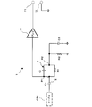
- FIG. 1 It is a perspective view which shows an example of the structure of the clamp type AC voltage probe which concerns on one Embodiment of this invention. It is a front view which showed the inside through see-through through the wall on the front side of a clamp arm and a housing shown in FIG. It is a circuit diagram which shows an example of the electric structure of the clamp type AC voltage probe shown in FIG. It is a circuit diagram which shows another example of the electrical structure of the clamp type AC voltage probe shown in FIG.
- the clamp-type AC voltage probe 1 shown in FIG. 1 roughly includes a clamp portion 2 that clamps the cable CBL to be measured, and a substantially box-shaped housing 3 that is connected to the clamp portion 2.
- the housing 3 is connected to a measuring device such as an oscilloscope or a data logger via a coaxial cable 4. Twice
- the clamp portion 2 includes a pair of clamp arms 21 and 22.
- the base end portion of the clamp arm 21 is pivotally supported by a shaft body 27 attached to the housing 3.
- the clamp arm 21 is swingable around the shaft body 27. Holding grooves 211 and 221 into which the cable CBL is fitted are formed on the facing surfaces of the clamp arms 21 and 22. Twice
- the clamp arm 21 is urged toward the clamp arm 22 by a torsion spring (not shown).
- the urging force of the torsion spring clamps the cable CBL between the clamp arm 21 and the clamp arm 22. Twice
- the clamp arm 22 is fixedly connected to the housing 3.
- the clamp arm 22 may be swingable like the clamp arm 21. Twice
- the clamp arms 21 and 22 and the housing 3 are made of an insulating material, for example, a resin material. Twice
- a storage space 28 is provided inside the clamp arm 22.
- the accommodation space 28 communicates with the internal space of the housing 3.
- a substantially plate-shaped electrode E is arranged in the accommodation space 28.
- the electrode E may be formed as a conductor pattern on a printed wiring board, for example, or may be a metal plate.
- the electrode E is arranged so as to face or contact the inner wall surface of the holding groove 221 of the clamp arm 22. As a result, the electrodes E are arranged so as to face the cable CBL clamped by the clamp portion 2 via the wall of the holding groove 221 made of the insulating material. Twice
- the circuit board 31 is housed in the housing 3.
- the terminal T3 of the circuit board 31 and the electrode E are connected via the wiring W. Twice
- the conductive layer 32 indicated by hatching is provided on the accommodation space 28 of the clamp arm 22 and the inner wall surface of the housing 3, except for a portion located between the cable CBL clamped by the clamp portion 2 and the electrode E. Is formed. Twice
- the conductive layer 32 may be, for example, a metal foil such as an aluminum foil, may be coated with a conductive paint, may be a plating layer, or may be a metal plate. In the example shown in FIG. 2, the conductive layer 32 is not formed on the wall of the holding groove 221 located between the cable CBL clamped by the clamp portion 2 and the electrode E, and the peripheral portion of the electrode E. Twice
- the outer wall surface of the clamp-type AC voltage probe 1 is made insulating, and between the cable CBL clamped by at least the clamp portion 2 on the inner wall surface of the housing 3 and the inner wall surface of the clamp arm 22, and the electrode E.
- the part excluding the located part is considered to be conductive. Twice
- the outer wall surface of the clamp type AC voltage probe 1 is insulated, for example, even if the conductor portion of the cable CBL is exposed, a current flows from the cable CBL to the electrode E and the circuit board 31 to clamp the cable CBL. The risk of damage to the AC voltage probe 1 is reduced. In addition, the safety of the user who operates the clamp type AC voltage probe 1 is improved. Twice
- the electrode E is not necessarily limited to the example in which the electrode E is arranged inside the clamp portion 2 and is arranged so as to face the cable CBL via an insulating material.
- the electrode E may be arranged so as to be exposed in, for example, the holding groove 221 and may be arranged so as to face each other in contact with the cable CBL. Twice
- the clamp type AC voltage probe 1 detects the AC voltage of the cable CBL via the capacitance Cx generated by arranging the conductor wire of the cable CBL and the electrode E so as to face each other.
- the capacitance Cx is inversely proportional to the facing distance d between the conductor wire of the cable CBL and the electrode E. Therefore, the shorter the facing distance d, the larger the capacitance Cx, and the easier it is to detect the AC voltage. Further, when the facing distance d changes, the voltage level obtained via the capacitance Cx fluctuates. Twice
- the clamping force of the cable CBL is insufficient only by the urging force of the torsion spring shown in the drawing, and a gap is generated between the cable CBL and the holding groove 221 to increase the facing distance d.
- the capacitance Cx may decrease. Further, the cable CBL may fluctuate, the facing distance d may fluctuate, and the capacitance Cx may fluctuate. Twice
- the clamp arms 21 and 22 can be fastened with screws 25 to firmly clamp the cable CBL, so that the capacitance Cx can be reduced due to the increase in the facing distance d and the cable can be reduced. It is possible to reduce the possibility that the capacitance Cx fluctuates due to the shaking of the CBL. Twice
- the nut 26 may be provided on the screw hole 23 side, and the screw 25 may be inserted through the screw hole 24. Further, a screw groove may be formed in the screw hole 23 or the screw hole 24 without providing the nut 26. Twice
- the clamp type AC voltage probe 1 shown in FIG. 3 includes an electrode E, a parallel circuit 5, a resistor R2 (second resistor), a capacitor C2 (second capacitor), an amplifier A1, and terminals T1 and T2.
- the parallel circuit 5 is a parallel circuit of the capacitor C1 (first capacitor) and the resistor R1 (first resistor).
- the parallel circuit 5, the resistor R2, the capacitor C2, the amplifier A1, and the terminals T1 and T2 are formed on the circuit board 31. Twice
- the electrode E is connected to one end P1 of the parallel circuit 5 via the wiring W shown in FIG. 2 and the terminal T3.
- the other end P2 of the parallel circuit 5 is connected to the circuit ground via the capacitor C2. Further, the other end P2 of the parallel circuit 5 is connected to the circuit ground via the resistor R2.
- the circuit ground is connected to the conductive layer 32. Twice
- One end P1 of the parallel circuit 5 is connected to the input terminal of the amplifier A1.
- the output terminal of the amplifier A1 is connected to the terminal T1.
- Terminal T2 is connected to the circuit ground. Twice
- the terminal T1 is connected to the core wire of the coaxial cable 4, and the terminal T2 is connected to the shielded wire of the coaxial cable 4.
- the output signal of the amplifier A1 is output to a measuring device such as an oscilloscope or a data logger via the coaxial cable 4.
- the output signal of the amplifier A1 is not limited to the example of being output via the coaxial cable, and may be a twisted pair cable, a multi-core cable, or the like. Further, the output signal line of the amplifier A1 and the operation power supply line of the amplifier A1 and the like may be included in one cable. From the viewpoint of reducing the influence of noise, it is more preferable that a cable for supplying an operating power source for the amplifier A1 or the like is provided separately from the cable for the output signal of the amplifier A1. Twice
- the cable CBL is not particularly limited, but for example, a power cable for driving a motor of an electric vehicle is assumed.
- the AC voltage of a square wave periodic waveform by PWM (Pulse Width Modulation) output from an inverter is the measurement target.
- the assumed voltage is AC200V to 1000V
- the measurement waveform is a pulse corresponding to a frequency of 1kHz to 1MHz. Twice
- the AC voltage of the cable CBL is applied to one end P1 of the parallel circuit 5 via the capacitance Cx. Twice
- a series circuit of the resistor R1 and the capacitor C2 is configured.
- the series circuit of the resistor R1 and the capacitor C2 is a so-called integrator circuit, and functions as a low-pass filter for passing low frequency components. Twice
- the series circuit of the resistor R1 and the capacitor C2 corresponds to the period of the square wave.
- the low frequency component to be used can be input to the amplifier A1. Twice
- a series circuit of the capacitor C1 and the resistor R2 is configured.
- the series circuit of the capacitor C1 and the resistor R2 is a so-called differentiating circuit, and functions as a high-pass filter for passing high frequency components. Twice
- the capacitor C1 and the resistor R are applied. According to the series circuit of 2, the high frequency component corresponding to the rising and falling edges of the rectangular wave can be input to the amplifier A1.
- both the low frequency component corresponding to the period of the square wave and the high frequency component corresponding to the rise and fall of the square wave are superimposed and input to the input terminal of the amplifier A1. Therefore, the AC voltage waveform detected from the cable CBL can be accurately amplified by the amplifier A1 and output to the measuring device. Twice
- the resistance value R 1 of the resistor R1 is much larger than the impedance of the capacitor C1.
- the resistance value R 1 can be set to 1 M ⁇ to 1 G ⁇ .
- Z of the capacitor C1 when the frequency f is 1 MHz. 1M ⁇ / 159 ⁇ 6300 times or more larger than
- Va Vin ⁇ (CxC 2 + CxC 1 ) / (C 1 C 2 + CxC 2 + CxC 1 ) ... (1)
- the capacitance of the capacitor C1 is C 1 and the capacitance of the capacitor C 2 is C 2. ..
- the cable voltage Vin is divided and the input voltage Va whose voltage is reduced is input to the amplifier A1. Therefore, as described in Patent Document 1, it is high. It becomes easy to measure a high voltage AC voltage without providing a circuit for generating a voltage. Twice
- the capacitance Cx can be 0.1 to 10 pF
- the capacitance C 1 can be 0.1 to 10 nF
- the capacitance C 2 can be 1 to 100 nF.
- Va Vin ⁇ 0.001 according to the equation (1).
- Va Vin ⁇ 0.001 according to the equation (1).
- the input voltage Va whose cable voltage Vin is reduced to 1/1000 can be input to the amplifier A1.
- the input voltage Va input to the amplifier A1 is 1 V, so that it is easy to measure the high voltage cable voltage Vin. Twice
- the amplifier A1 is a so-called amplifier circuit that amplifies and outputs an input signal.
- the amplifier A1 preferably has an element having a high input impedance, and for example, an amplifier configured by using FETs such as a junction FET (Field Effect Transistor) and a MOSFET (Metal-Oxide-Semiconductor FET) can be preferably used. .. Twice
- the AC current detected by the electrode E from the cable CBL flows through the series circuit of the capacitance Cx and the capacitors C1 and C2, so that the cable voltage Vin is divided and the input voltage Va is transferred to the amplifier A1. Entered. However, if the input impedance of the amplifier A1 is small, the detected alternating current flows into the amplifier A1, the current flowing through the series circuit of the capacitance Cx and the capacitors C1 and C2 decreases, and the input voltage Va decreases. Therefore, the detection accuracy of the cable voltage Vin may be lowered. Twice
- the output signal of the amplifier A1 is output to the measuring device via the terminal T1 and the coaxial cable 4. This makes it possible to observe the AC voltage waveform of the cable CBL with a measuring device. Twice
- the input terminal of the amplifier A1 may be connected to the other end P2 instead of one end P1.
- the filter characteristics of a low-pass filter composed of a resistor R1 and a capacitor C2 and a high-pass filter composed of a capacitor C1 and a resistor R2 depending on the frequency and waveform of the signal to be detected.
- the input terminal of the amplifier A1 is connected to the other end P2. If this is done, the detection level input to the amplifier A1 will change. Twice
- the input terminal of the amplifier A1 when the input terminal of the amplifier A1 is once connected to P1, if the capacitance of the capacitors C1 and C2 is adjusted within the range where the series impedance of the capacitors C1 and C2 does not change, the detection level input to the amplifier A1 can be adjusted. It is possible to adjust the filter characteristics while suppressing changes. Therefore, the input terminal of the amplifier A1 may be connected to the other end P2, but it is more preferable to connect the input terminal to the other end P1. Twice
- the clamp-type AC voltage probe includes a clamp portion that clamps the cable to be measured, an electrode arranged so as to face the cable clamped by the clamp portion, and a first capacitor.
- the first resistor are connected in parallel, one end is connected to the electrode, and the second resistor, one end is connected to the other end of the parallel circuit and the other end is connected to the circuit ground, and the parallel A second capacitor having one end connected to the other end of the circuit and the other end connected to the circuit ground, and the one end or the other end of the parallel circuit connected to the input terminal and input to the input terminal. It is equipped with an amplifier that amplifies and outputs. Twice
- the core wire of the cable and the electrode are arranged to face each other, and the electrode is electrostatically coupled to the core wire of the cable.
- the AC voltage of the cable is applied to one end of the parallel circuit through the capacitance generated between the core wire of the cable and the electrode.
- the first resistor and the second capacitor are connected in series to form a low-pass filter, and the first capacitor and the second resistor are connected in series to form a high-pass filter.
- the basic frequency of the AC voltage to be measured is acquired by the low-pass filter, and the high-frequency components included in the waveforms such as the rising and falling edges of the AC voltage are acquired by the high-pass filter, so that the waveform to be measured is accurately obtained.
- the input terminal of the amplifier is connected to the one end of the parallel circuit. Twice
- the voltage division ratio of the voltage input to the amplifier is determined by the series impedance of the first capacitor and the second capacitor.
- the voltage division ratio of the voltage input to the amplifier is determined by the impedance of the second capacitor. Therefore, if the capacitance of the second capacitor is changed in order to adjust the characteristics of the low-pass filter, the signal level input to the amplifier also changes.
- the voltage division ratio of the voltage input to the amplifier is determined by the series impedance of the first capacitor and the second capacitor, so that the series impedance of the first and second capacitors is not changed within the range of the second capacitor.
- the resistance value of the first resistor is preferably larger than the impedance of the first capacitor. Twice
- the input terminal of the amplifier has a high impedance. Twice
- the amplifier is configured by using FET. Twice
- the input impedance of the FET is high impedance, it is suitable as the above-mentioned amplifier. Twice
- the clamp portion is configured by using an insulating material, the electrodes are arranged inside the clamp portion, and are arranged so as to face the cable via the insulating material. Twice
- a housing connected to the clamp portion and accommodating the parallel circuit, the second resistor, the second capacitor, and the amplifier is further provided, and the outer wall surface of the housing is insulating and the inner wall surface is conductive. It is preferable that the circuit ground is connected to the conductive inner wall surface. Twice
- the outer wall surface of the housing touched by the user is made insulating to improve safety, and the conductive inner wall surface can reduce electromagnetic noise from the external environment. Twice
- the clamp portion has a storage space for accommodating the electrode, the outer wall surface of the clamp portion is insulating, and the inner wall surface of the accommodation space is a portion located at least between the electrode and the cable. Except for this, it is considered to be conductive, and it is preferable that the circuit ground is connected to the conductive inner wall surface of the accommodation space. Twice
- the outer wall surface of the clamp portion touched by the user is made insulating to improve safety, and the conductive portion of the inner wall surface can reduce electromagnetic noise from the external environment. Twice
- the clamp portion clamps the cable by a pair of clamp arms, at least one base end portion of the pair of clamp arms is pivotally supported by a shaft body, and the at least one clamp arm holds the shaft body. It is preferable that a screw hole that can swing at the center and can accept a screw for fastening the pair of clamp arms is formed in the vicinity of the tips of the pair of clamp arms. Twice
- the cable can be firmly clamped by the pair of clamp arms. Therefore, a gap is less likely to occur between the cable and the clamp arm, and the capacitance between the cable electrodes is stable. As a result, the cable voltage can be easily detected by the clamp type AC voltage probe.
Landscapes
- Physics & Mathematics (AREA)
- General Physics & Mathematics (AREA)
- Measuring Instrument Details And Bridges, And Automatic Balancing Devices (AREA)
- Measurement Of Current Or Voltage (AREA)
Priority Applications (4)
| Application Number | Priority Date | Filing Date | Title |
|---|---|---|---|
| JP2022505889A JP7632452B2 (ja) | 2020-03-13 | 2021-02-22 | クランプ式交流電圧プローブ |
| DE112021001624.5T DE112021001624T5 (de) | 2020-03-13 | 2021-02-22 | Wechselspannungsfühler des klemmtyps |
| US17/910,362 US12092662B2 (en) | 2020-03-13 | 2021-02-22 | Clamp-type AC voltage probe |
| CN202180019733.8A CN115244409A (zh) | 2020-03-13 | 2021-02-22 | 夹紧式交流电压探头 |
Applications Claiming Priority (2)
| Application Number | Priority Date | Filing Date | Title |
|---|---|---|---|
| JP2020044778 | 2020-03-13 | ||
| JP2020-044778 | 2020-03-13 |
Publications (1)
| Publication Number | Publication Date |
|---|---|
| WO2021182082A1 true WO2021182082A1 (ja) | 2021-09-16 |
Family
ID=77671612
Family Applications (1)
| Application Number | Title | Priority Date | Filing Date |
|---|---|---|---|
| PCT/JP2021/006518 Ceased WO2021182082A1 (ja) | 2020-03-13 | 2021-02-22 | クランプ式交流電圧プローブ |
Country Status (5)
| Country | Link |
|---|---|
| US (1) | US12092662B2 (https=) |
| JP (1) | JP7632452B2 (https=) |
| CN (1) | CN115244409A (https=) |
| DE (1) | DE112021001624T5 (https=) |
| WO (1) | WO2021182082A1 (https=) |
Families Citing this family (1)
| Publication number | Priority date | Publication date | Assignee | Title |
|---|---|---|---|---|
| USD1096465S1 (en) * | 2024-04-19 | 2025-10-07 | Hopkins Manufacturing Corporation | Wire testing device |
Citations (9)
| Publication number | Priority date | Publication date | Assignee | Title |
|---|---|---|---|---|
| JPS5986322A (ja) * | 1982-10-04 | 1984-05-18 | テクトロニックス・インコーポレイテッド | 減衰器補償装置 |
| JPH04276561A (ja) * | 1991-03-04 | 1992-10-01 | Advantest Corp | 周波数特性校正装置 |
| JP2002090394A (ja) * | 2000-09-12 | 2002-03-27 | Yokogawa Electric Corp | 電圧測定回路及びその校正方法 |
| JP2002271159A (ja) * | 2001-03-13 | 2002-09-20 | Shibasoku:Kk | アッテネータの周波数特性調整回路 |
| JP2010025653A (ja) * | 2008-07-17 | 2010-02-04 | Hioki Ee Corp | 測定装置 |
| JP2013120098A (ja) * | 2011-12-06 | 2013-06-17 | Irt:Kk | 電圧検出装置及び電力検出装置 |
| JP2017032287A (ja) * | 2015-07-29 | 2017-02-09 | 日置電機株式会社 | クランプ式センサおよび測定装置 |
| JP2019023627A (ja) * | 2017-07-10 | 2019-02-14 | テクトロニクス・インコーポレイテッドTektronix,Inc. | 試験測定プローブ及び試験測定プローブの校正方法 |
| US20200041549A1 (en) * | 2018-08-02 | 2020-02-06 | Aclara Technologies, Llc | Medium voltage sensor using a multi-component resistive voltage divider |
Family Cites Families (10)
| Publication number | Priority date | Publication date | Assignee | Title |
|---|---|---|---|---|
| US6646562B1 (en) * | 2002-05-28 | 2003-11-11 | Appa Technology Corp. | Hooking-type fully automatic electric meter |
| JP2010025918A (ja) | 2008-06-18 | 2010-02-04 | Hioki Ee Corp | 電圧検出装置および線間電圧検出装置 |
| CN103975247B (zh) * | 2011-10-07 | 2016-08-24 | 弗劳恩霍夫应用研究促进协会 | 具有虚假峰值拒绝的峰值检测器 |
| US20130208761A1 (en) * | 2012-02-14 | 2013-08-15 | General Tools And Instruments | Instrument with Non-contact Infrared Temperature Measurement and Current Clamp |
| WO2013150896A1 (ja) * | 2012-04-04 | 2013-10-10 | 株式会社村田製作所 | 磁気検出装置および紙幣識別装置 |
| US10338102B2 (en) * | 2012-06-01 | 2019-07-02 | Mitsubishi Electric Corporation | Voltage detection device for transforming apparatus |
| WO2014087469A1 (ja) * | 2012-12-03 | 2014-06-12 | 三菱電機株式会社 | 電圧検出装置 |
| JP5687311B2 (ja) * | 2013-06-21 | 2015-03-18 | 三菱電機株式会社 | 電圧測定回路 |
| JP6576154B2 (ja) * | 2015-08-06 | 2019-09-18 | 日置電機株式会社 | 電圧検出センサおよび測定装置 |
| JP6508163B2 (ja) * | 2016-10-31 | 2019-05-08 | 横河電機株式会社 | 電流測定装置 |
-
2021
- 2021-02-22 DE DE112021001624.5T patent/DE112021001624T5/de active Pending
- 2021-02-22 JP JP2022505889A patent/JP7632452B2/ja active Active
- 2021-02-22 CN CN202180019733.8A patent/CN115244409A/zh active Pending
- 2021-02-22 US US17/910,362 patent/US12092662B2/en active Active
- 2021-02-22 WO PCT/JP2021/006518 patent/WO2021182082A1/ja not_active Ceased
Patent Citations (9)
| Publication number | Priority date | Publication date | Assignee | Title |
|---|---|---|---|---|
| JPS5986322A (ja) * | 1982-10-04 | 1984-05-18 | テクトロニックス・インコーポレイテッド | 減衰器補償装置 |
| JPH04276561A (ja) * | 1991-03-04 | 1992-10-01 | Advantest Corp | 周波数特性校正装置 |
| JP2002090394A (ja) * | 2000-09-12 | 2002-03-27 | Yokogawa Electric Corp | 電圧測定回路及びその校正方法 |
| JP2002271159A (ja) * | 2001-03-13 | 2002-09-20 | Shibasoku:Kk | アッテネータの周波数特性調整回路 |
| JP2010025653A (ja) * | 2008-07-17 | 2010-02-04 | Hioki Ee Corp | 測定装置 |
| JP2013120098A (ja) * | 2011-12-06 | 2013-06-17 | Irt:Kk | 電圧検出装置及び電力検出装置 |
| JP2017032287A (ja) * | 2015-07-29 | 2017-02-09 | 日置電機株式会社 | クランプ式センサおよび測定装置 |
| JP2019023627A (ja) * | 2017-07-10 | 2019-02-14 | テクトロニクス・インコーポレイテッドTektronix,Inc. | 試験測定プローブ及び試験測定プローブの校正方法 |
| US20200041549A1 (en) * | 2018-08-02 | 2020-02-06 | Aclara Technologies, Llc | Medium voltage sensor using a multi-component resistive voltage divider |
Also Published As
| Publication number | Publication date |
|---|---|
| JPWO2021182082A1 (https=) | 2021-09-16 |
| DE112021001624T5 (de) | 2022-12-29 |
| CN115244409A (zh) | 2022-10-25 |
| US12092662B2 (en) | 2024-09-17 |
| US20230127522A1 (en) | 2023-04-27 |
| JP7632452B2 (ja) | 2025-02-19 |
Similar Documents
| Publication | Publication Date | Title |
|---|---|---|
| JP7182510B2 (ja) | 振動センサを有する非接触dc電圧測定装置 | |
| EP3143416B1 (en) | A partial discharge acquisition system comprising a capacitive coupling electric field sensor | |
| JP5909785B2 (ja) | イオン平衡測定及び調整のための遮蔽されたコンデンサ回路を有する電離平衡装置 | |
| TWI745478B (zh) | 用於非接觸式電壓測量裝置的傳感器子系統 | |
| JP6495103B2 (ja) | 電圧検出プローブおよび測定装置 | |
| CN105026939B (zh) | 计测装置以及安装单元 | |
| JP7128298B2 (ja) | 車両の乗員室内部の乗員の有無を検出するためのデバイス | |
| JP2018132346A (ja) | 電圧検出装置 | |
| JP7632452B2 (ja) | クランプ式交流電圧プローブ | |
| CN110780122B (zh) | 电导率仪 | |
| WO2014155680A1 (ja) | 電圧測定装置 | |
| JP2009053074A (ja) | 電界検出装置 | |
| AU1146299A (en) | Device for testing circuit boards | |
| TWI905382B (zh) | 電壓測定裝置 | |
| CN113607999B (zh) | 隔离差分电路、差分探头和示波器组件 | |
| JP6576154B2 (ja) | 電圧検出センサおよび測定装置 | |
| JP4676643B2 (ja) | 電位固定装置および容量測定装置 | |
| JP2018091798A (ja) | 水分量検出器 | |
| JP5019097B2 (ja) | 電子部品の特性測定装置及び電子部品の特性値測定方法 | |
| JP5716249B2 (ja) | 測定システムのためのアダプタ・コンポーネント | |
| JP5232389B2 (ja) | 空間分布された被保護インピーダンス | |
| JP2018205032A (ja) | 帯電プレートモニタ装置 | |
| JP2015010973A (ja) | 抵抗保持機構、実装基板および測定装置 | |
| JP2019105512A (ja) | 電気伝導度推定装置 | |
| KR970071023A (ko) | 인쇄회로기판에 장착된 집적회로(ic)의 리드 들뜸 검출장치 |
Legal Events
| Date | Code | Title | Description |
|---|---|---|---|
| 121 | Ep: the epo has been informed by wipo that ep was designated in this application |
Ref document number: 21767807 Country of ref document: EP Kind code of ref document: A1 |
|
| ENP | Entry into the national phase |
Ref document number: 2022505889 Country of ref document: JP Kind code of ref document: A |
|
| 122 | Ep: pct application non-entry in european phase |
Ref document number: 21767807 Country of ref document: EP Kind code of ref document: A1 |