WO2021182071A1 - 通信装置 - Google Patents
通信装置 Download PDFInfo
- Publication number
- WO2021182071A1 WO2021182071A1 PCT/JP2021/006278 JP2021006278W WO2021182071A1 WO 2021182071 A1 WO2021182071 A1 WO 2021182071A1 JP 2021006278 W JP2021006278 W JP 2021006278W WO 2021182071 A1 WO2021182071 A1 WO 2021182071A1
- Authority
- WO
- WIPO (PCT)
- Prior art keywords
- conductor
- circuit
- voltage
- resistor
- communication device
- Prior art date
- Legal status (The legal status is an assumption and is not a legal conclusion. Google has not performed a legal analysis and makes no representation as to the accuracy of the status listed.)
- Ceased
Links
Images


Classifications
-
- H—ELECTRICITY
- H03—ELECTRONIC CIRCUITRY
- H03M—CODING; DECODING; CODE CONVERSION IN GENERAL
- H03M1/00—Analogue/digital conversion; Digital/analogue conversion
- H03M1/66—Digital/analogue converters
-
- H—ELECTRICITY
- H04—ELECTRIC COMMUNICATION TECHNIQUE
- H04B—TRANSMISSION
- H04B3/00—Line transmission systems
- H04B3/54—Systems for transmission via power distribution lines
- H04B3/548—Systems for transmission via power distribution lines the power on the line being DC
-
- H—ELECTRICITY
- H03—ELECTRONIC CIRCUITRY
- H03H—IMPEDANCE NETWORKS, e.g. RESONANT CIRCUITS; RESONATORS
- H03H7/00—Multiple-port networks comprising only passive electrical elements as network components
- H03H7/01—Frequency selective two-port networks
- H03H7/06—Frequency selective two-port networks including resistors
-
- H—ELECTRICITY
- H04—ELECTRIC COMMUNICATION TECHNIQUE
- H04B—TRANSMISSION
- H04B15/00—Suppression or limitation of noise or interference
- H04B15/005—Reducing noise, e.g. humm, from the supply
-
- H—ELECTRICITY
- H04—ELECTRIC COMMUNICATION TECHNIQUE
- H04B—TRANSMISSION
- H04B3/00—Line transmission systems
- H04B3/02—Details
- H04B3/30—Reducing interference caused by unbalanced currents in a normally balanced line
-
- H—ELECTRICITY
- H04—ELECTRIC COMMUNICATION TECHNIQUE
- H04B—TRANSMISSION
- H04B3/00—Line transmission systems
- H04B3/54—Systems for transmission via power distribution lines
-
- H—ELECTRICITY
- H04—ELECTRIC COMMUNICATION TECHNIQUE
- H04B—TRANSMISSION
- H04B3/00—Line transmission systems
- H04B3/54—Systems for transmission via power distribution lines
- H04B3/56—Circuits for coupling, blocking, or by-passing of signals
-
- H—ELECTRICITY
- H04—ELECTRIC COMMUNICATION TECHNIQUE
- H04L—TRANSMISSION OF DIGITAL INFORMATION, e.g. TELEGRAPHIC COMMUNICATION
- H04L25/00—Baseband systems
- H04L25/02—Details ; arrangements for supplying electrical power along data transmission lines
-
- H—ELECTRICITY
- H04—ELECTRIC COMMUNICATION TECHNIQUE
- H04L—TRANSMISSION OF DIGITAL INFORMATION, e.g. TELEGRAPHIC COMMUNICATION
- H04L25/00—Baseband systems
- H04L25/02—Details ; arrangements for supplying electrical power along data transmission lines
- H04L25/03—Shaping networks in transmitter or receiver, e.g. adaptive shaping networks
-
- H—ELECTRICITY
- H05—ELECTRIC TECHNIQUES NOT OTHERWISE PROVIDED FOR
- H05K—PRINTED CIRCUITS; CASINGS OR CONSTRUCTIONAL DETAILS OF ELECTRIC APPARATUS; MANUFACTURE OF ASSEMBLAGES OF ELECTRICAL COMPONENTS
- H05K5/00—Casings, cabinets or drawers for electric apparatus
- H05K5/0091—Housing specially adapted for small components
-
- H—ELECTRICITY
- H05—ELECTRIC TECHNIQUES NOT OTHERWISE PROVIDED FOR
- H05K—PRINTED CIRCUITS; CASINGS OR CONSTRUCTIONAL DETAILS OF ELECTRIC APPARATUS; MANUFACTURE OF ASSEMBLAGES OF ELECTRICAL COMPONENTS
- H05K7/00—Constructional details common to different types of electric apparatus
- H05K7/02—Arrangements of circuit components or wiring on supporting structure
Definitions
- the present disclosure relates to communication devices.
- This application claims priority based on Japanese Application No. 2020-040059 filed on March 9, 2020, and incorporates all the contents described in the Japanese application.
- Patent Document 1 discloses a communication system for a vehicle in which a plurality of communication devices communicate with each other.
- the communication device described in Patent Document 1 is an ECU (Electronic Control Unit), and receives a differential signal represented by a difference between two voltages.
- a differential signal is input to the analog circuit.
- the reference potential of the analog circuit (reference of zero V) is the ground potential.
- the analog circuit performs analog processing on the input differential signal.
- the communication circuit receives the differential signal that has been analog-processed by the analog circuit.
- the communication circuit converts the received differential signal into a single-ended signal whose reference potential is the ground potential, and outputs the converted single-ended signal.
- the communication device has a first conductor and a second conductor, and a circuit element connected to the first conductor, and processes a differential signal represented by a voltage difference between the two conductors.
- An analog circuit to be applied, a connection circuit including other circuit elements other than a capacitor, and a connection circuit connected to the analog circuit, and a differential signal processed by the analog circuit are received and received via the connection circuit.
- a conductive storage box in which the first conductor, the second conductor, the analog circuit, the connection circuit, the communication circuit, and the connection element are housed, and the storage box is inside the first conductor and the second conductor. It conducts to a conductor with a large surface area.
- FIG. It is a block diagram which shows the main part structure of a communication device. It is an exploded view of a communication device. It is a top view of a communication device. It is a side view of a communication device. It is sectional drawing of a communication device. It is a top view of a circuit board. It is explanatory drawing of the effect of a containment box. It is explanatory drawing of an analog circuit. It is explanatory drawing of the detection circuit. It is explanatory drawing of arrangement of a resistor. It is a top view of the circuit board in Embodiment 2. It is sectional drawing of the communication apparatus in Embodiment 2. FIG.
- the communication device has a first conductor and a second conductor, and a circuit element connected to the first conductor, and is a differential signal represented by a voltage difference between the two conductors.
- a connection circuit including an analog circuit to be processed and other circuit elements other than a capacitor and connected to the analog circuit, and a differential signal processed by the analog circuit are received via the connection circuit.
- a communication circuit that generates a signal whose reference potential is the potential of the second conductor based on the received differential signal, and a circuit element different from the capacitor, which is connected between the first conductor and the second conductor.
- the first conductor, the second conductor, the analog circuit, the connection circuit, the communication circuit, and the conductive storage box in which the connection element is housed are provided, and the storage box includes the first conductor and the second conductor. It conducts to a conductor with a large surface surface among the conductors.
- the analog circuit transmits an analog-processed differential signal to the communication circuit via a connection circuit including other circuit elements other than the capacitor, for example, an inductor or a resistor.
- a connecting element such as an inductor or a resistor is connected between the first conductor and the second conductor.
- the high frequency noise entering the analog circuit and the communication circuit is small. Further, the high frequency noise emitted from the analog circuit and the communication circuit to the outside is also small.
- the storage box is conducted to one of the first conductor and the second conductor, which has a larger surface area. Therefore, the stray capacitance formed between the storage box and the other conductor and the stray capacitance formed between the first conductor and the second conductor are small. As a result, the high frequency noise that enters the communication circuit from the analog circuit via the stray capacitance is small, and the high frequency noise that enters the analog circuit from the communication circuit via the stray capacitance is also small.
- the surface area of the second conductor is larger than the surface area of the first conductor.
- the surface area of the first conductor connected to the analog circuit is small, and the surface area of the second conductor connected to the communication circuit is large.
- the communication device includes a resistor, an input circuit into which a voltage is input via the resistor, and a first capacitor connected between one end of the resistor and the first conductor. , The other end of the resistor and a second capacitor connected between the second conductors.
- each of the resistor and the connecting element suppresses the propagation of high frequency noise through itself. Therefore, when the high-frequency noise enters the first conductor, the high-frequency noise propagating in the order of the first capacitor and the resistor is small, and the high-frequency noise entering the first conductor to the second conductor is also small. When the high frequency noise enters the second conductor, the high frequency noise propagating in the order of the second capacitor and the resistor is small, and the high frequency noise entering the first conductor from the second conductor is also small.
- the communication device is a detection that detects the connection of the external device to the connector based on the connector detachably connected to the external device and the voltage input to the input circuit.
- a voltage is input to the input circuit via the connector and a resistor, and the detection unit detects the connection of the external device when the voltage input to the input circuit is equal to or higher than the threshold voltage. ..
- connection of the external device to the connector is detected when the voltage input to the input circuit via the connector and the resistor is equal to or higher than the threshold voltage.
- the distance between the resistor and the first conductor coincides with the distance between the resistor and the second conductor.
- the resistor is arranged so that the distance from the first conductor and the distance from the second conductor match. Therefore, the distance between the first conductor and the second conductor is long, and the stray capacitance formed between the first conductor and the second conductor is even smaller.
- the analog circuit has a termination circuit for preventing reflection of the differential signal, and the termination circuit is in the middle of two conducting wires through which the differential signal propagates. , Is connected to the first conductor.
- the termination circuit is connected to the middle of the two conductors through which the differential signal propagates and to the first conductor.
- the termination circuit prevents reflection of the differential signal.
- connection circuit has a common mode choke coil, and the communication circuit transmits a differential signal via the connection circuit.
- connection circuit has a common mode choke coil.
- the common mode choke coil has two inductors. Each of the two inductors is located in the middle of two conductors connecting an analog circuit and a communication circuit. The differential signal propagates through the two conductors.
- the common mode choke coil removes common mode noise from the differential signal propagating from the analog circuit to the communication circuit, and removes common mode noise from the differential signal propagating from the communication circuit to the analog circuit.
- the communication device includes a remover that removes noise from a DC voltage whose reference potential is the potential of the first conductor, and the remover has a reference potential of the second conductor.
- a voltage having the potential of the above and from which noise has been removed is applied to a power line for power supply, the remover has an inductor, and the inductor is the connecting element.
- the remover removes noise from the voltage whose reference potential is the potential of the first conductor, and applies a voltage whose reference potential is the potential of the second conductor and the noise is removed to the power line.
- the remover is, for example, a common mode choke coil and has an inductor. This inductor is connected between the first conductor and the second conductor as a connecting element.
- FIG. 1 is an explanatory diagram of an outline of the communication device 10 according to the present embodiment.
- the communication device 10 is an ECU (Electronic Control Unit), a gateway, or the like, and is mounted on a vehicle.
- the communication device 10 includes a connector 20.
- the connector 20 is detachably connected to the cable 11 or the connector 12a of the diagnostic tool 12.
- the communication device 10 When the cable 11 is connected to the connector 20 of the communication device 10, electric power is supplied to the communication device 10 via the cable 11 and the communication device 10 operates.
- the communication device 10 transmits / receives a differential signal to / from another communication device (not shown) via the cable 11.
- the communication device 10 performs transmission / reception based on a communication standard called Broad-Reach, a communication standard of CAN (Controller Area Network), or the like.
- the communication device 10 is, for example, an ECU that controls the operation of a motor that locks and unlocks the door of the vehicle
- the communication device 10 receives a differential signal instructing the unlocking of the door
- the communication device 10 receives. Have the motor unlock the door.
- the communication device 10 transmits a differential signal indicating the detection result of the sensor to another communication device. And notify the detection result.
- the diagnostic tool 12 supplies power to the communication device 10.
- the communication device 10 operates.
- the communication device 10 and the diagnostic tool 12 communicate with each other.
- the communication device 10 transmits a differential signal including data used for detecting a failure, so-called log data, to the diagnostic tool 12.
- the diagnostic tool 12 transmits a differential signal including update data for updating a computer program executed by the communication device 10 to the communication device 10.
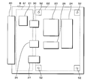
- FIG. 2 is a block diagram showing a main configuration of the communication device 10.
- the communication device 10 includes an analog circuit 21, a connection circuit 22, a communication circuit 23, a microcomputer (hereinafter referred to as a microcomputer) 24, a common mode choke coil 25, a regulator 26, a detection circuit 27, and a first conductor G1. And a second conductor G2. These are connected by conductors.
- the conductors used for power supply, that is, the power lines, are shown by thick solid lines.
- Each of the first conductor G1 and the second conductor G2 has conductivity and is made of, for example, metal.
- the connection circuit 22 has a common mode choke coil 30.
- the common mode choke coil 30 has a first inductor 30a and a second inductor 30b.
- the first inductor 30a and the second inductor 30b are wound around an annular magnetic material (not shown).
- the common mode choke coil 25 has a first inductor 25a and a second inductor 25b.
- the common mode choke coil 25 is configured in the same manner as the common mode choke coil 30.
- the connector 20 is connected to the analog circuit 21 by two conductors. Further, one end of the first inductor 30a and the second inductor 30b of the common mode choke coil 30 is connected to the analog circuit 21 by two conducting wires.
- the analog circuit 21 is further connected to the first conductor G1 by a conducting wire. The connection to the first conductor G1 is so-called grounding.
- the other ends of the first inductor 30a and the second inductor 30b of the common mode choke coil 30 are connected to the communication circuit 23 by two conductors.
- the communication circuit 23 is further connected to the microcomputer 24 and the second conductor G2 by two conductors. The connection to the second conductor G2 is also so-called grounding.
- the connector 20 is further connected to one end of the first inductor 25a of the common mode choke coil 25 by a conducting wire.
- the connector 20 is further connected to one end of the second inductor 25b of the common mode choke coil 25 and the first conductor G1 by a conducting wire.
- the other end of the first inductor 25a is connected to the regulator 26 by a conducting wire.
- the other end of the second inductor 25b is connected to the second conductor G2 by a conducting wire.
- the regulator 26 is further connected to the microcomputer 24 and the second conductor G2 by two conductors.
- the microcomputer 24 is further connected to the second conductor G2 by a conducting wire.
- the connector 20 is further connected to the detection circuit 27 and the first conductor G1 by two conductors.
- the detection circuit 27 is further connected to the microcomputer 24, the first conductor G1 and the second conductor G2 by three conductors.
- the cable 11 When the cable 11 is connected to the connector 20, the cable 11 is connected to the analog circuit 21, the common mode choke coil 25, and the first conductor G1. In the conducting wire connecting the connector 20 and the detection circuit 27, one end on the connector 20 side is opened.
- the connector 12a of the diagnostic tool 12 When the connector 12a of the diagnostic tool 12 is connected to the connector 20, the connector 12a of the diagnostic tool 12 is connected to the analog circuit 21, the common mode choke coil 25, the detection circuit 27, and the first conductor G1.
- the differential signal is input from the cable 11 or the diagnostic tool 12 to the analog circuit 21 via the connector 20.
- the differential signal is a binary signal and is represented by the voltage difference between the two conductors. For example, a voltage difference greater than or equal to a predetermined value represents a differential signal "0", and a voltage difference less than a predetermined value represents a differential signal "1".
- the differential signal propagates through the two conductors.
- the reference potential of the analog circuit 21 (reference of zero V) is the potential of the first conductor G1.
- the analog circuit 21 performs analog processing on the differential signal input from the connector 20.
- the communication circuit 23 receives the differential signal subjected to analog processing by the analog circuit 21 via the common mode choke coil 30 of the connection circuit 22.
- the common mode choke coil 30 removes common mode noise from the differential signal subjected to analog processing by the analog circuit 21, and outputs the differential signal from which the common mode noise has been removed to the communication circuit 23.
- Common mode noise is noise that is superimposed in phase on two conductors through which a differential signal propagates.
- the connection circuit 22 includes other circuit elements other than the capacitor.
- the communication circuit 23 generates a single-ended signal whose reference potential is the potential of the second conductor G2 based on the received differential signal, and outputs the generated single-ended signal to the microcomputer 24.
- the microcomputer 24 reads the voltage of the single-ended signal input from the communication circuit 23. As a result, the microcomputer 24 acquires the data included in the single-ended signal.
- the microcomputer 24 executes various processes based on the data included in the single-ended signal input from the communication circuit 23.
- the microcomputer 24 outputs a single-ended signal whose reference potential is the potential of the second conductor G2 to the communication circuit 23.
- the communication circuit 23 generates a differential signal based on the single-ended signal input from the microcomputer 24.
- the communication circuit 23 transmits the generated differential signal to a communication device or a diagnostic tool 12 (not shown) via the connection circuit 22, the analog circuit 21, and the connector 20.
- the common mode choke coil 30 of the connection circuit 22 removes common mode noise from the differential signal transmitted by the communication circuit 23.
- the common mode choke coil 30 outputs a differential signal from which common mode noise has been removed via the analog circuit 21 and the connector 20.
- a DC voltage whose reference potential is the potential of the first conductor G1 is input from the cable 11 or the diagnostic tool 12 to the common mode choke coil 25 via the connector 20.
- the common mode choke coil 25 removes common mode noise from the voltages input to the first inductor 25a and the second inductor 25b.
- the voltage from which the common mode choke coil 25 has removed the common mode noise is a voltage whose reference potential is the potential of the second conductor G2.
- the common mode choke coil 25 applies a voltage from which common mode noise has been removed to a conducting wire connected to the regulator 26. As a result, the voltage from which the common mode noise is removed is output to the regulator 26.
- the common mode choke coil 25 functions as a remover. As shown in FIG. 2, the conductors connected between the connector 20 and the first inductor 25a, the conductors connected between the first inductor 25a and the regulator 26, and the conductors connected between the regulator 26 and the microcomputer 24 are It is a power line.
- the regulator 26 converts the DC voltage input from the common mode choke coil 25 into a preset set voltage.
- the set voltage is a DC voltage whose reference potential is the potential of the second conductor G2.
- the regulator 26 outputs the converted set voltage to the microcomputer 24. As a result, electric power is supplied to the microcomputer 24.
- the regulator 26 may further output a set voltage to the communication circuit 23 to supply electric power to the communication circuit 23.
- the diagnostic tool 12 When the connector 12a of the diagnostic tool 12 is connected to the connector 20, the diagnostic tool 12 continues to output a DC voltage whose reference potential is the potential of the first conductor G1 to the detection circuit 27.
- the voltage output by the diagnostic tool 12 is equal to or higher than a preset threshold voltage.
- zero V is output to the detection circuit 27.
- zero V is a voltage whose reference potential is the potential of the first conductor G1 and is less than the threshold voltage.
- the detection circuit 27 outputs a voltage based on the potential of the second conductor G2 to the microcomputer 24.
- the detection circuit 27 outputs zero V or a predetermined voltage Vc (see FIG. 10).
- the detection circuit 27 outputs zero V to the microcomputer 24 when the voltage input from the connector 20 is equal to or higher than the threshold voltage, that is, when the diagnostic tool 12 is connected.
- the detection circuit 27 outputs a predetermined voltage Vc to the microcomputer 24 when the voltage input from the connector 20 is less than the threshold voltage, that is, when the diagnostic tool 12 is not connected.
- the microcomputer 24 detects the connection of the connector 12a of the diagnostic tool 12 to the connector 20 based on the voltage input from the detection circuit 27.
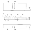
- FIG. 3 is an exploded view of the communication device 10.
- a connector 20, an analog circuit 21, a connection circuit 22, a communication circuit 23, a microcomputer 24, a common mode choke coil 25, a regulator 26, and a detection circuit 27 are arranged on the upper plate surface of the circuit board B.
- a connector 20, an analog circuit 21, a microcomputer 24, a regulator 26, and a detection circuit 27 are shown.
- the first conductor G1 and the second conductor G2 are arranged in the circuit board B.
- the connector 20 is arranged at the leading edge portion on the front side of the circuit board B. A part of the connector 20 projects to the front side of the leading edge.
- the conductive path is a so-called circuit pattern.
- the connection to the first conductor G1 or the second conductor G2 is realized by using the through hole and the conductive path.
- a guide foil is attached to the surface of the through hole.
- the guide foil is conductive with the conductive path.
- a conducting wire is formed by both the conducting foil and the conductive path, or by the conductive path.
- FIG. 4 is a plan view of the communication device 10.
- FIG. 5 is a side view of the communication device 10.
- FIG. 6 is a cross-sectional view of the communication device 10.
- the analog circuit 21, the connection circuit 22, the communication circuit 23, the microcomputer 24, the common mode choke coil 25, the regulator 26, the detection circuit 27, and the circuit board B are conductive. It is housed in the storage box 4.
- the storage box 4 is made of metal, for example.
- the storage box 4 is composed of a conductive upper covering body 4a that covers the upper plate surface of the circuit board B and a conductive lower covering body 4b that covers the lower plate surface of the circuit board B.
- Each of the upper covering body 4a and the lower covering body 4b has a box shape with one side open.
- the upper covering body 4a is arranged so that the bottom wall is on the upper side.
- the lower covering body 4b is arranged so that the bottom wall is on the lower side.
- the edge of the opening surface of the upper covering body 4a is in contact with the edge of the opening surface of the lower covering body 4b.
- the upper plate surface of the circuit board B is arranged inside the upper covering body 4a.
- the lower plate surface of the circuit board B is arranged inside the lower covering body 4b.
- the bottom wall of the upper covering body 4a is formed with recesses 40a and 41a recessed downward.
- the bottom wall of the upper covering body 4a has a rectangular shape and faces the upper plate surface of the circuit board B.
- Each of the two recesses 40a is provided in the middle of the left side portion and the right side portion of the bottom surface of the upper covering body 4a.
- the entire rear side portion of the bottom wall of the upper covering body 4a is recessed, whereby the recess 41a is formed.
- the bottom wall of the lower covering body 4b is formed with recesses 40b and 41b recessed on the upper side.
- the bottom wall of the lower covering body 4b has a rectangular shape and faces the lower plate surface of the circuit board B.
- Each of the two recesses 40a is provided in the middle of the left side portion and the right side portion of the bottom wall of the lower covering body 4b.
- the entire rear side portion of the bottom wall of the lower covering body 4b is recessed, whereby the recess 41b is formed.
- the bottom surfaces of the recesses 40a and 41a of the upper covering body 4a face each other of the bottom surfaces of the recesses 40b and 41b of the lower covering body 4b.
- the upper covering body 4a is provided with four through holes 42a penetrating in the vertical direction. As shown in FIG. 4, each of the two through holes 42a is provided in the bottom wall of the two recesses 40a. The remaining two through holes 42a are provided on the left side and the right side of the recess 41a, respectively.
- the lower covering body 4b is also provided with four through holes 42b penetrating in the vertical direction. Each of the two through holes 42b is provided in the bottom wall of the two recesses 40b. The remaining two through holes 42b are provided on the left side and the right side of the recess 41b, respectively.
- Each of the four through holes 42a of the upper covering body 4a faces the four through holes 42b of the lower covering body 4b.
- FIG. 7 is a plan view of the circuit board B. As shown in FIGS. 6 and 7, the second conductor G2 is exposed at each of the four locations on the upper plate surface of the circuit board B. The second conductor G2 is also exposed at each of the four locations on the lower plate surface of the circuit board B. The four exposed surfaces of the second conductor G2 on the lower plate surface of the circuit board B are arranged below each of the four exposed surfaces of the second conductor G2 on the upper plate surface of the circuit board B.
- Screw holes 52 penetrating in the vertical direction are provided on each of the four exposed surfaces of the second conductor G2.
- each of the four screw 50s is inserted into the four screw holes 52 in a state where the screw portions of the four screws 50 are passed through the four through holes 42a of the upper covering body 4a from above. Tighten the four screws 50.
- the peripheral edge of the through hole 42a of the upper covering body 4a is sandwiched between the head of the screw 50 and the circuit board B.
- the peripheral edge of the through hole 42a of the upper covering body 4a comes into contact with the second conductor G2, and the upper covering body 4a conducts to the second conductor G2.
- the screw portions of the four screws 50 project to the lower side of the circuit board B.
- the screw portions of the four screw 50s protruding downward passing through the four through holes 42b of the lower covering body 4b from above, four nuts 51 are inserted into the screw portions of each of the four screw 50s. Attach from the tip.
- the peripheral edge of the through hole 42b of the lower covering body 4b is sandwiched between the nut 51 and the circuit board B.
- the peripheral edge of the through hole 42b of the lower covering body 4b comes into contact with the second conductor G2, and the lower covering body 4b conducts to the second conductor G2.
- the upper covering body 4a is conducting with the lower covering body 4b via the second conductor G2.
- the four screws 50 and the four nuts 51 are conductive and are made of, for example, metal.
- the edge of the opening surface of the upper covering body 4a is in contact with the edge of the opening surface of the lower covering body 4b.
- the upper covering body 4a is directly connected to the lower covering body 4b at the edge portion.
- the front wall of the upper covering body 4a is provided with an opening (not shown) that penetrates in the front-rear direction.
- the connector 20 is inserted through the opening of the upper covering body 4a and protrudes to the front side of the storage box 4.
- the circuit board B has a rectangular shape, and the first conductor G1 and the second conductor G2 each have a rectangular plate shape.
- the plate surfaces of the first conductor G1 and the second conductor G2 face the plate surface of the circuit board B.
- the surface area of the second conductor G2 is larger than the surface area of the first conductor G1.
- the first conductor G1 and the second conductor G2 are arranged in the front-rear direction.
- the first conductor G1 and the second conductor G2 are covered with an insulating resin in a state where they are not in contact with each other.
- the analog circuit 21 connected to the first conductor G1 and not connected to the second conductor G2 is arranged above the first conductor G1.
- the common mode choke coil 25 and the detection circuit 27 connected to both the first conductor G1 and the second conductor G2 are arranged above the first conductor G1 and the second conductor G2.
- the common mode choke coil 30 of the connection circuit 22 that is not connected to both the first conductor G1 and the second conductor G2 is also arranged above the first conductor G1 and the second conductor G2.
- the communication circuit 23, the microcomputer 24, and the regulator 26, which are not connected to the first conductor G1 and are connected to the second conductor G2, are arranged above the second conductor G2.
- FIG. 8 is an explanatory diagram of the effect of the storage box 4.
- the analog circuit 21, the connection circuit 22, the communication circuit 23, the microcomputer 24, the common mode choke coil 25, the regulator 26, the detection circuit 27, and the circuit board B are housed in the conductive storage box 4. Therefore, the high frequency noise generated outside the communication device 10 is difficult to enter into the communication device 10, and the high frequency noise entering the analog circuit 21, the communication circuit 23, the microcomputer 24, the detection circuit 27, and the like is small.
- high frequency noise is generated with the generation of static electricity.
- high frequency noise is generated by the interference of an electromagnetic field generated when a signal propagates through a conducting wire arranged in the vicinity of the communication device 10.
- the first conductor G1 does not conduct to the storage box 4 and the second conductor G2. Therefore, a capacitive coupling occurs between the storage box 4 and the first conductor G1, and a capacitive coupling occurs between the first conductor G1 and the second conductor G2.
- capacitive coupling occurs, stray capacitance is formed.
- the storage box 4 conducts to the second conductor G2, which has a surface area larger than the surface area of the first conductor G1. Therefore, the stray capacitance formed between the storage box 4 and the first conductor G1 having a small surface area is small, and the stray capacitance formed between the first conductor G1 and the second conductor G2 is also small.
- the high frequency noise entering the circuit connected to the second conductor G2 from the circuit connected to the first conductor G1 via the stray capacitance is small.
- High-frequency noise entering the circuit connected to the first conductor G1 from the circuit connected to the second conductor G2 via the stray capacitance is also small.
- FIG. 9 is an explanatory diagram of the analog circuit 21.
- the analog circuit 21 has a termination circuit 60 and capacitors 61 and 62.
- the termination circuit 60 is connected to the middle of the two conductors through which the differential signal propagates and to the first conductor G1.
- One end of the capacitor 61 is connected to the connector 20 and the termination circuit 60.
- the other end of the capacitor 61 is connected to one end of the first inductor 30a of the common mode choke coil 30.
- One end of the capacitor 62 is connected to the connector 20 and the termination circuit 60.
- the other end of the capacitor 62 is connected to one end of the second inductor 30b of the common mode choke coil 30.
- the termination circuit 60 executes analog processing to prevent reflection of the differential signal propagating through the two conductors.
- the reference potential of the terminal circuit 60 is the potential of the first conductor G1.
- the termination circuit 60 has resistors 70, 71, 72 and a capacitor 73. One end of each of the resistors 70 and 71 is connected to one end of the capacitors 61 and 62. The other ends of the resistors 70 and 71 are connected to one end of the capacitor 73. The other end of the capacitor 73 is connected to the first conductor G1.
- a resistor 72 is connected between both ends of the capacitor 73.
- the resistance value of the resistor 70 is a resistance value in consideration of the characteristic impedance of the propagation path of the signal propagating through the conducting wire connected to one end of the resistor 70.
- the other end of the resistor 70 is grounded via the capacitor 73. Therefore, the reflection of the signal propagating through the conducting wire connected to one end of the resistor 70 is prevented.
- the resistance value of the resistor 71 is a resistance value in consideration of the characteristic impedance of the propagation path of the signal propagating through the conducting wire connected to one end of the resistor 71.
- the other end of the resistor 71 is grounded via the capacitor 73. Therefore, the reflection of the signal propagating through the conducting wire connected to one end of the resistor 71 is prevented.
- the resistors 70 and 71 prevent reflection of the differential signal propagating through the two conductors.
- the analog processing performed by the analog circuit 21 is a processing for preventing the reflection of the differential signal, and the reference potential is the potential of the first conductor G1.
- the capacitor 73 is arranged to remove noise propagating through the two conductors. Noise propagates from the two conductors to the first conductor G1 via the capacitor 73. The capacitor 73 discharges the stored electric power through the resistor 72.
- Capacitors 61 and 62 are used for AC (Alternating Current) coupling, respectively. Each of the capacitors 61 and 62 removes the DC component from the signal input from one end via the conducting wire, and outputs the signal from which the DC component has been removed from the other end. Therefore, the capacitors 61 and 62 remove the DC component from the differential signal input via the connector 20, and also remove the DC component from the differential signal transmitted by the communication circuit 23.
- AC Alternating Current
- the communication device 10 may contain externally generated high-frequency noise.
- the reference potential is a predetermined potential, for example, the voltage of the first conductor G1, which is the potential of the ground, fluctuates at high speed.
- the current flowing through the resistors 70 and 71 cannot follow the fluctuation of the voltage of the first conductor G1. Therefore, in the two conductors on the analog circuit 21 side of the common mode choke coil 30, the voltage based on the potential of the first conductor G1 fluctuates at high speed as the voltage of the first conductor G1 fluctuates. As a result, high-frequency noise enters the analog circuit 21.
- the second inductor 25b of the common mode choke coil 25 is connected between the first conductor G1 and the second conductor G2. Therefore, even when the voltage of the first conductor G1 whose reference potential is a predetermined potential fluctuates, the voltage of the second conductor G2 whose reference potential is a predetermined potential hardly fluctuates.
- the second inductor 25b functions as a connecting element.
- the first inductor 30a of the common mode choke coil 30 is arranged in the middle of one of the conducting wires connecting the analog circuit 21 and the communication circuit 23.
- the second inductor 30b of the common mode choke coil 30 is arranged in the middle of the other conducting wire connecting the analog circuit 21 and the communication circuit 23. Therefore, even if the voltages of the two conductors fluctuate on the analog circuit 21 side of the common mode choke coil 30, the voltages of the two conductors almost fluctuate on the communication circuit 23 side of the common mode choke coil 30. There is no such thing.
- each of the common mode choke coils 25 and 30 suppresses the propagation of high frequency noise through itself.
- the high frequency noise entering the communication circuit 23 from the analog circuit 21 is small.
- the reference potential is a predetermined potential, for example, the voltage of the second conductor G2, which is the potential of the ground, fluctuates at high speed.
- the current flowing through the second conductor G2 via the communication circuit 23 cannot follow the fluctuation of the voltage of the second conductor G2. Therefore, in the two conductors on the communication circuit 23 side of the common mode choke coil 30, the voltage whose reference potential is the potential of the second conductor G2 fluctuates at high speed as the voltage of the second conductor G2 fluctuates. As a result, high frequency noise enters the communication circuit 23.
- the first conductor G1 and the second conductor G2 are connected by the second inductor 25b of the common mode choke coil 25. Therefore, even when the voltage of the second conductor G2 whose reference potential is a predetermined potential fluctuates, the voltage of the first conductor G1 whose reference potential is a predetermined potential hardly fluctuates.
- the first inductor 30a of the common mode choke coil 30 is arranged in the middle of one of the conducting wires connecting the analog circuit 21 and the communication circuit 23.
- the second inductor 30b of the common mode choke coil 30 is arranged in the middle of the other conducting wire connecting the analog circuit 21 and the communication circuit 23. Therefore, even if the voltages of the two conductors fluctuate on the communication circuit 23 side of the common mode choke coil 30, the voltages of the two conductors almost fluctuate on the analog circuit 21 side of the common mode choke coil 30. There is no such thing.
- each of the common mode choke coils 25 and 30 suppresses the propagation of high frequency noise through itself.
- the high frequency noise entering the analog circuit 21 from the communication circuit 23 is small.
- the storage box 4 is conductive with the second conductor G2. Therefore, the entry of high-frequency noise into the storage box 4 is equivalent to the entry of high-frequency noise into the second conductor G2.
- the volume of the conductor composed of the storage box 4 and the second conductor G2 is large. Therefore, the impedance of the conductor composed of the storage box 4 and the second conductor G2 is small. As a result, the fluctuation of the voltage of the second conductor G2 that occurs when the storage box 4 contains the high frequency noise or when the second conductor G2 contains the high frequency noise is small.
- FIG. 10 is an explanatory diagram of the detection circuit 27.
- the detection circuit 27 has resistors 80, 81, 82, capacitors 83, 84 and an input circuit 85.
- the input circuit 85 has an NPN type bipolar transistor 90 and a resistor 91.
- One end of the resistor 80 is connected to the connector 20, one end of the resistor 81 and the capacitor 83.
- the other ends of the resistor 81 and the capacitor 83 are connected to the first conductor G1.
- the other end of the resistor 80 is connected to the base of the bipolar transistor 90 included in the input circuit 85 and one end of the resistor 82 and the capacitor 84.
- the other ends of the resistor 82 and the capacitor 84 are connected to the second conductor G2.
- the capacitor 83 is connected to one end of the resistor 80 and between the first conductor G1.
- the capacitor 84 is connected between the other end of the resistor 80 and the second conductor G2.
- Capacitors 83 and 84 function as first and second capacitors, respectively.
- the collector of the bipolar transistor 90 is connected to one end of the resistor 91.
- a predetermined voltage Vc is applied to the other end of the resistor 91.
- the predetermined voltage Vc is a constant voltage whose reference potential is the potential of the second conductor G2.
- the predetermined voltage Vc may be, for example, a set voltage output by the regulator 26. In this case, the regulator 26 applies a predetermined voltage Vc to the other end of the resistor 91.
- the collector of the bipolar transistor 90 is further connected to the microcomputer 24.
- the emitter of the bipolar transistor 90 is connected to the second conductor G2.
- the bipolar transistor 90 functions as a switch. When the current flows in the bipolar transistor 90 in the order of the base and the emitter, the bipolar transistor 90 is switched on. When the bipolar transistor 90 is on, the resistance value between the collector and the emitter is sufficiently small, and the current flows in the order of the resistor 91 and the bipolar transistor 90. In the bipolar transistor 90, when the current flow through the base and the emitter is stopped, the bipolar transistor 90 is switched off. When the bipolar transistor 90 is off, the resistance value between the collector and the emitter is sufficiently large, and the current does not flow in the order of the resistor 91 and the bipolar transistor 90.
- the current flows in the bipolar transistor 90 in the order of the base and the emitter, and the bipolar transistor 90 is on.
- the voltage input from the connector 20 is a voltage whose reference potential is the potential of the first conductor G1.
- the voltage input from the connector 20 is less than the above-mentioned threshold voltage, the current does not flow in the bipolar transistor 90 in the order of the base and the emitter, and the bipolar transistor 90 is off.
- the diagnostic tool 12 detects a voltage whose reference potential is the potential of the first conductor G1 and which is equal to or higher than the threshold voltage 27. Output to. At this time, the current flows from the positive terminal of the diagnostic tool 12 in the order of the resistor 80, the base and emitter of the bipolar transistor 90, the second conductor G2, the second inductor 25b and the first conductor G1 to the negative terminal of the diagnostic tool 12. return. As a result, the bipolar transistor is switched on, and the current flows in the input circuit 85 in the order of the resistor 91, the bipolar transistor 90, and the second conductor G2. As a result, the input circuit 85 outputs zero V to the microcomputer 24. Zero V is a voltage whose reference potential is the potential of the second conductor G2.
- the diagnostic tool 12 when the diagnostic tool 12 is connected to the connector 20, it outputs a DC voltage to the base of the bipolar transistor 90 of the input circuit 85 via the connector 20 and the resistor 80. At this time, the input circuit 85 outputs zero V to the microcomputer 24.
- zero V is output to the detection circuit 27.
- zero V is a voltage whose reference potential is the potential of the first conductor G1 and is less than the threshold voltage.
- the current flow through the base and the emitter of the bipolar transistor 90 is stopped, and the bipolar transistor 90 is switched off.
- a predetermined voltage Vc is input to the microcomputer 24.
- a voltage equal to or higher than the threshold voltage or zero V is input to the base of the bipolar transistor 90 of the input circuit 85 via the resistor 80.
- the input circuit 85 outputs zero V to the microcomputer 24.
- the input circuit 85 outputs a predetermined voltage Vc to the microcomputer 24.
- the microcomputer 24 detects the connection of the diagnostic tool 12 to the connector 20 based on the voltage input from the input circuit 85, that is, the voltage input to the input circuit 85 via the connector 20 and the resistor 80. Specifically, the microcomputer 24 detects the connection of the diagnostic tool 12 when the voltage input to the input circuit 85 is equal to or higher than the threshold voltage.
- Each of the diagnostic tool 12 and the microcomputer 24 functions as an external device and a detection unit.
- the resistor 80 limits the magnitude of the current flowing in the order of the base and the emitter in the bipolar transistor 90. Therefore, the resistance value of the resistor 80 is relatively large.
- the resistor 81 stabilizes the voltage input from the connector 20.
- the resistor 82 stabilizes the voltage between the emitter and the base in the bipolar transistor 90.
- the capacitor 83 smoothes the voltage output from the connector 20 toward the resistor 80.
- the capacitor 84 smoothes the voltage output from the connector 20 via the resistor 80.
- the first conductor G1 and the second conductor G2 are connected by the second inductor 25b of the common mode choke coil 25. Therefore, even when the voltage of the first conductor G1 whose reference potential is a predetermined potential fluctuates, the voltage of the second conductor G2 whose reference potential is a predetermined potential hardly fluctuates.
- one end of the resistor 80 on the connector 20 side is connected to the first conductor G1 via the resistor 81.
- One end of the resistor 80 on the input circuit 85 side is connected to the second conductor G2 via the resistor 82. Therefore, even if the voltage at one end of the resistor 80 on the connector 20 side fluctuates, the voltage at one end of the resistor 80 on the input circuit 85 side hardly fluctuates.
- the voltage of the second conductor G2 whose reference potential is a predetermined potential fluctuates at high speed.
- the current flowing through the capacitor 84 cannot follow the fluctuation of the voltage of the second conductor G2. Therefore, at one end of the resistor 80 on the connector 20 side, the voltage whose reference potential is the potential of the second conductor G2 fluctuates at high speed as the voltage of the second conductor G2 fluctuates.
- the first conductor G1 and the second conductor G2 are connected by the second inductor 25b of the common mode choke coil 25. Therefore, even when the voltage of the second conductor G2 whose reference potential is a predetermined potential fluctuates, the voltage of the first conductor G1 whose reference potential is a predetermined potential hardly fluctuates.
- one end of the resistor 80 on the connector 20 side is connected to the first conductor G1 via the resistor 81.
- One end of the resistor 80 on the input circuit 85 side is connected to the second conductor G2 via the resistor 82. Therefore, even if the voltage at one end of the resistor 80 on the input circuit 85 side fluctuates, the voltage at one end of the resistor 80 on the connector 20 side hardly fluctuates.
- each of the common mode choke coil 25 and the resistor 80 suppresses the propagation of high frequency noise through itself. Therefore, when the high-frequency noise enters the first conductor G1, the high-frequency noise propagating in the order of the capacitor 83 and the resistor 80 is small, and the high-frequency noise entering the first conductor G1 to the second conductor G2 is also small. Further, when the high frequency noise enters the second conductor G2, the high frequency noise propagating in the order of the capacitor 84 and the resistor 80 is small, and the high frequency noise entering the first conductor G1 from the second conductor G2 is also small.
- FIG. 11 is an explanatory diagram of the arrangement of the resistors 80.
- the upper side of FIG. 11 shows a part of the plate surface of the circuit board B.
- the lower side of FIG. 11 shows a part of the cross section of the circuit board B.
- the resistor 80 has a rectangular parallelepiped shape, and in a plan view, the resistor 80 is arranged at the center between the first conductor G1 and the second conductor G2.
- the end faces of the first conductor G1 and the second conductor G2 face each other along the longitudinal direction of the resistor 80.
- the distance between the resistor 80 and the first conductor G1 is the same as the distance between the resistor 80 and the second conductor G2.
- "match" does not mean an exact match, but a substantial match.
- the distance between the resistor 80 and the first conductor G1 coincides with the distance between the resistor 80 and the second conductor G2.
- match does not mean an exact match, but a substantive match.
- the resistor 80 is arranged so that the distance from the first conductor G1 and the distance from the second conductor G2 match. Therefore, the distance between the first conductor G1 and the second conductor G2 is long, and the stray capacitance formed between the first conductor G1 and the second conductor G2 is even smaller.
- the second conductor G2 exposed on the upper side and the lower side of the circuit board B is in contact with the storage box 4.
- the portion of the second conductor G2 that comes into contact with the storage box 4 is not limited to the portion exposed on the upper side and the lower side of the circuit board B.
- the second embodiment will be described as different from the first embodiment.
- Other configurations except the configuration described later are common to the first embodiment. Therefore, the components common to the first embodiment are designated by the same reference numerals as those of the first embodiment, and the description thereof will be omitted.
- FIG. 12 is a plan view of the circuit board B according to the second embodiment.
- FIG. 13 is a cross-sectional view of the communication device 10 according to the second embodiment.
- the cross section shown in FIG. 13 is a cross section in the left-right direction.
- the right end surface and the left end surface of the second conductor G2 are exposed.
- the right end surface and the left end surface of the second conductor G2 are in contact with the upper covering body 4a constituting the storage box 4.
- the communication device 10 according to the second embodiment similarly exhibits the effect of the communication device 10 according to the first embodiment.
- the storage box 4 may be in contact with the second conductor G2. Therefore, the method of bringing the storage box 4 into contact with the second conductor G2 is a method of contacting the storage box 4 with the surfaces of the second conductor G2 exposed on the upper and lower sides, or the end surface of the second conductor G2. The method of contacting the storage box 4 with the container 4 is not limited to the method.
- the configuration of the storage box 4 is not limited to the configuration in which the edge of the opening surface of the upper covering body 4a contacts the edge of the opening surface of the lower covering body 4b.
- the upper covering body 4a may cover the upper side of the outer surface of the lower covering body 4b. In this case, the inner surface of the upper covering body 4a comes into contact with the outer surface of the lower covering body 4b.
- the storage box 4 is not limited to the box composed of the upper covering body 4a and the lower covering body 4b.
- the first conductor G1 and the storage box 4 may be made conductive instead of the second conductor G2.
- the communication circuit 23 transmits / receives a differential signal not only when the cable 11 is connected to the connector 20 but also when the diagnostic tool 12 is connected to the connector 20.
- the communication circuit that the diagnostic tool 12 transmits and receives when the diagnostic tool 12 is connected to the connector 20 may be a communication circuit different from the communication circuit 23.
- the communication circuit further has the same configuration as the analog circuit 21, the connection circuit 22, and the communication circuit 23.
- the communication standard of the communication performed by the diagnostic tool 12 may be different from the communication standard of the communication performed via the cable 11.
- the circuit element included in the connection circuit 22 is not limited to the common mode choke coil 30, and may be a circuit element different from the capacitor.
- two resistors may be arranged in the middle of each of the two conductors connecting the analog circuit 21 and the communication circuit 23.
- the connecting element connected between the first conductor G1 and the second conductor G2 is not limited to the second inductor 25b, and may be a circuit element different from the capacitor.
- a resistor may be connected between the first conductor G1 and the second conductor G2.
- the regulator 26 is connected to the connector 20 via an inductor. This inductor removes noise from the voltage.
- the voltage output by the diagnostic tool 12 to the input circuit 85 via the resistor 80 is not limited to the DC voltage indicating the connection, and may be the voltage related to the communication signal. That is, the diagnostic tool 12 may transmit a communication signal to the microcomputer 24 via the input circuit 85.
- the analog processing performed by the analog circuit 21 may be analog processing based on the potential of the first conductor G1. Therefore, the analog processing performed by the analog circuit 21 is not limited to the processing for preventing the reflection of the differential signal.
- the analog processing performed by the analog circuit 21 may be, for example, a processing for removing noise. In this case, for example, in the analog circuit 21, one end of two capacitors is connected in the middle of each of the two conductors through which the differential signal propagates, and the other end of the two capacitors is connected to the first conductor G1.
Landscapes
- Engineering & Computer Science (AREA)
- Computer Networks & Wireless Communication (AREA)
- Signal Processing (AREA)
- Power Engineering (AREA)
- Microelectronics & Electronic Packaging (AREA)
- Theoretical Computer Science (AREA)
- Filters And Equalizers (AREA)
- Dc Digital Transmission (AREA)
Priority Applications (2)
| Application Number | Priority Date | Filing Date | Title |
|---|---|---|---|
| US17/905,369 US12088318B2 (en) | 2020-03-09 | 2021-02-19 | Communication apparatus |
| CN202180015994.2A CN115152186B (zh) | 2020-03-09 | 2021-02-19 | 通信装置 |
Applications Claiming Priority (2)
| Application Number | Priority Date | Filing Date | Title |
|---|---|---|---|
| JP2020040059A JP7310659B2 (ja) | 2020-03-09 | 2020-03-09 | 通信装置 |
| JP2020-040059 | 2020-03-09 |
Publications (1)
| Publication Number | Publication Date |
|---|---|
| WO2021182071A1 true WO2021182071A1 (ja) | 2021-09-16 |
Family
ID=77669292
Family Applications (1)
| Application Number | Title | Priority Date | Filing Date |
|---|---|---|---|
| PCT/JP2021/006278 Ceased WO2021182071A1 (ja) | 2020-03-09 | 2021-02-19 | 通信装置 |
Country Status (4)
| Country | Link |
|---|---|
| US (1) | US12088318B2 (https=) |
| JP (1) | JP7310659B2 (https=) |
| CN (1) | CN115152186B (https=) |
| WO (1) | WO2021182071A1 (https=) |
Cited By (1)
| Publication number | Priority date | Publication date | Assignee | Title |
|---|---|---|---|---|
| WO2025249196A1 (ja) * | 2024-05-28 | 2025-12-04 | 株式会社オートネットワーク技術研究所 | 車載装置 |
Families Citing this family (3)
| Publication number | Priority date | Publication date | Assignee | Title |
|---|---|---|---|---|
| US12520440B2 (en) * | 2021-03-30 | 2026-01-06 | Autonetworks Technologies, Ltd. | Communication device and communication apparatus |
| WO2022209843A1 (ja) * | 2021-03-30 | 2022-10-06 | 株式会社オートネットワーク技術研究所 | 通信器及び通信装置 |
| CN116884746A (zh) * | 2023-06-02 | 2023-10-13 | 英业达科技有限公司 | 隔离变压器 |
Citations (3)
| Publication number | Priority date | Publication date | Assignee | Title |
|---|---|---|---|---|
| JPH09275421A (ja) * | 1995-12-04 | 1997-10-21 | Fujitsu Ltd | 通信・情報端末装置 |
| JP2016096472A (ja) * | 2014-11-14 | 2016-05-26 | 株式会社オートネットワーク技術研究所 | 通信システム及びコネクタ |
| JP2020167536A (ja) * | 2019-03-29 | 2020-10-08 | 株式会社オートネットワーク技術研究所 | 通信装置 |
Family Cites Families (20)
| Publication number | Priority date | Publication date | Assignee | Title |
|---|---|---|---|---|
| JP2003046655A (ja) * | 2001-08-03 | 2003-02-14 | Matsushita Electric Ind Co Ltd | 2線式給電通信装置 |
| JP2004356918A (ja) * | 2003-05-29 | 2004-12-16 | Tdk Corp | ノイズ抑制回路 |
| JP2004362250A (ja) * | 2003-06-04 | 2004-12-24 | Fuji Electric Device Technology Co Ltd | 安定化電源回路 |
| JP4877998B2 (ja) * | 2007-03-30 | 2012-02-15 | ルネサスエレクトロニクス株式会社 | 半導体集積回路装置 |
| JP2009111911A (ja) | 2007-10-31 | 2009-05-21 | Toyota Motor Corp | 通信装置及び通信システム並びに通信方法 |
| JP5924284B2 (ja) * | 2012-03-16 | 2016-05-25 | 住友電気工業株式会社 | 通信装置及び通信システム |
| US9533638B2 (en) * | 2013-07-18 | 2017-01-03 | The Boeing Company | Aircraft universal power converter |
| JP6118304B2 (ja) * | 2014-11-14 | 2017-04-19 | 株式会社オートネットワーク技術研究所 | 通信システム及び通信装置 |
| US10382005B2 (en) * | 2016-07-25 | 2019-08-13 | Linear Technology Corporation | Communications system using hybrid common mode choke and kelvin sensing of voltage |
| US10444823B2 (en) * | 2016-07-25 | 2019-10-15 | Linear Technology Corporation | Communications system using hybrid common mode choke and kelvin sensing of voltage |
| JP6614109B2 (ja) * | 2016-11-21 | 2019-12-04 | 株式会社村田製作所 | 無線回路搭載電子機器 |
| US10027424B2 (en) * | 2016-11-22 | 2018-07-17 | Ciena Corporation | Low-latency adjustment of flexible transceivers using pilot signal |
| JP7155107B2 (ja) * | 2017-03-15 | 2022-10-18 | 株式会社村田製作所 | 回路モジュール、ネットワークモジュール、及び車載電子機器 |
| JP6911580B2 (ja) * | 2017-06-29 | 2021-07-28 | 富士電機株式会社 | スイッチング電源装置の制御回路 |
| DE102017009088A1 (de) * | 2017-09-29 | 2019-04-04 | WAGO Verwaltungsgesellschaft mit beschränkter Haftung | Schaltkreis zur Überprüfung einer analogen Eingangsschaltung eines A/D-Wandlers |
| JP2021028999A (ja) * | 2017-12-07 | 2021-02-25 | 日立オートモティブシステムズ株式会社 | 電子制御装置 |
| US10382216B1 (en) * | 2018-03-15 | 2019-08-13 | Linear Technology Holding Llc | Termination for wire pair carrying DC and differential signals |
| US10594519B2 (en) * | 2018-05-01 | 2020-03-17 | Linear Technology Holding Llc | Power over data lines system using pair of differential mode chokes for coupling DC voltage and attenuating common mode noise |
| US11418369B2 (en) * | 2019-08-01 | 2022-08-16 | Analog Devices International Unlimited Company | Minimizing DC bias voltage difference across AC-blocking capacitors in PoDL system |
| US11711591B2 (en) * | 2020-05-06 | 2023-07-25 | Marvell Asia Pte, Ltd. | Common-mode filtering for high-speed cable interface |
-
2020
- 2020-03-09 JP JP2020040059A patent/JP7310659B2/ja active Active
-
2021
- 2021-02-19 US US17/905,369 patent/US12088318B2/en active Active
- 2021-02-19 CN CN202180015994.2A patent/CN115152186B/zh active Active
- 2021-02-19 WO PCT/JP2021/006278 patent/WO2021182071A1/ja not_active Ceased
Patent Citations (3)
| Publication number | Priority date | Publication date | Assignee | Title |
|---|---|---|---|---|
| JPH09275421A (ja) * | 1995-12-04 | 1997-10-21 | Fujitsu Ltd | 通信・情報端末装置 |
| JP2016096472A (ja) * | 2014-11-14 | 2016-05-26 | 株式会社オートネットワーク技術研究所 | 通信システム及びコネクタ |
| JP2020167536A (ja) * | 2019-03-29 | 2020-10-08 | 株式会社オートネットワーク技術研究所 | 通信装置 |
Cited By (1)
| Publication number | Priority date | Publication date | Assignee | Title |
|---|---|---|---|---|
| WO2025249196A1 (ja) * | 2024-05-28 | 2025-12-04 | 株式会社オートネットワーク技術研究所 | 車載装置 |
Also Published As
| Publication number | Publication date |
|---|---|
| JP7310659B2 (ja) | 2023-07-19 |
| US20230119130A1 (en) | 2023-04-20 |
| CN115152186A (zh) | 2022-10-04 |
| US12088318B2 (en) | 2024-09-10 |
| JP2021141543A (ja) | 2021-09-16 |
| CN115152186B (zh) | 2024-04-09 |
Similar Documents
| Publication | Publication Date | Title |
|---|---|---|
| WO2021182071A1 (ja) | 通信装置 | |
| JP7226021B2 (ja) | 通信装置 | |
| US11046195B2 (en) | Apparatus for transmitting energy and information by means of a charging cable for an electric vehicle | |
| US20030153205A1 (en) | Audio jack | |
| JPH09312488A (ja) | 車載用コントロールユニットのemi用接地構造 | |
| CN114630947B (zh) | 用于在至少两个不同的探测区域内探测激活行为的车辆用装置 | |
| JP2013528831A (ja) | ディスプレイのための回路基板ならびにディスプレイおよび回路基板を有するディスプレイモジュール | |
| US12323274B2 (en) | Differential transmission substrate and power-over-differential data communication device | |
| JP5147501B2 (ja) | 車載電子装置 | |
| JP2013030722A (ja) | 接続構造および接続方法 | |
| US11258208B2 (en) | Module for a high-current plug and/or a high-current cable, high-current plug, and method of influencing the EMC behaviour | |
| JP5370935B2 (ja) | 電力変換装置及びフィルタスイッチ | |
| US12061222B2 (en) | Detecting device and manufacturing method | |
| CN114728630B (zh) | 用于与移动设备通信的车辆的装置 | |
| CN115299184B (zh) | 电路基板及电子设备 | |
| CN112119678A (zh) | 电子装置和搭载有电子装置的电动助力转向装置 | |
| US12520440B2 (en) | Communication device and communication apparatus | |
| JPH08148877A (ja) | 電子機器用遮蔽装置 | |
| US10592458B1 (en) | Bimodal impedance matching terminators | |
| US8664537B2 (en) | Method and apparatus for reducing signal noise | |
| JP5672277B2 (ja) | 電子装置 | |
| US8391518B2 (en) | Condenser microphone | |
| EP3735115B1 (en) | Input connection device | |
| JPWO2011021339A1 (ja) | 給電線構造及びそれを用いた回路基板、emiノイズ低減方法 | |
| JP2000180488A (ja) | 駆動デバイス用の電磁ノイズ評価装置 |
Legal Events
| Date | Code | Title | Description |
|---|---|---|---|
| 121 | Ep: the epo has been informed by wipo that ep was designated in this application |
Ref document number: 21767076 Country of ref document: EP Kind code of ref document: A1 |
|
| NENP | Non-entry into the national phase |
Ref country code: DE |
|
| 122 | Ep: pct application non-entry in european phase |
Ref document number: 21767076 Country of ref document: EP Kind code of ref document: A1 |