WO2021166073A1 - To-can型光半導体モジュール - Google Patents
To-can型光半導体モジュール Download PDFInfo
- Publication number
- WO2021166073A1 WO2021166073A1 PCT/JP2020/006307 JP2020006307W WO2021166073A1 WO 2021166073 A1 WO2021166073 A1 WO 2021166073A1 JP 2020006307 W JP2020006307 W JP 2020006307W WO 2021166073 A1 WO2021166073 A1 WO 2021166073A1
- Authority
- WO
- WIPO (PCT)
- Prior art keywords
- lead pin
- optical semiconductor
- conductor pattern
- stem
- type optical
- Prior art date
- Legal status (The legal status is an assumption and is not a legal conclusion. Google has not performed a legal analysis and makes no representation as to the accuracy of the status listed.)
- Ceased
Links
Images



Classifications
-
- H—ELECTRICITY
- H01—ELECTRIC ELEMENTS
- H01S—DEVICES USING THE PROCESS OF LIGHT AMPLIFICATION BY STIMULATED EMISSION OF RADIATION [LASER] TO AMPLIFY OR GENERATE LIGHT; DEVICES USING STIMULATED EMISSION OF ELECTROMAGNETIC RADIATION IN WAVE RANGES OTHER THAN OPTICAL
- H01S5/00—Semiconductor lasers
- H01S5/02—Structural details or components not essential to laser action
- H01S5/022—Mountings; Housings
-
- H—ELECTRICITY
- H10—SEMICONDUCTOR DEVICES; ELECTRIC SOLID-STATE DEVICES NOT OTHERWISE PROVIDED FOR
- H10F—INORGANIC SEMICONDUCTOR DEVICES SENSITIVE TO INFRARED RADIATION, LIGHT, ELECTROMAGNETIC RADIATION OF SHORTER WAVELENGTH OR CORPUSCULAR RADIATION
- H10F77/00—Constructional details of devices covered by this subclass
-
- H—ELECTRICITY
- H10—SEMICONDUCTOR DEVICES; ELECTRIC SOLID-STATE DEVICES NOT OTHERWISE PROVIDED FOR
- H10W—GENERIC PACKAGES, INTERCONNECTIONS, CONNECTORS OR OTHER CONSTRUCTIONAL DETAILS OF DEVICES COVERED BY CLASS H10
- H10W76/00—Containers; Fillings or auxiliary members therefor; Seals
- H10W76/10—Containers or parts thereof
Definitions
- the present disclosure relates to a TO-CAN type optical semiconductor module in which an optical semiconductor is mounted in a Transistor Outline (TO) -CAN type package.
- TO Transistor Outline
- the high frequency characteristics when transmitting a high frequency electric signal applied from the outside to the optical semiconductor are important, especially from the viewpoint of packaging.
- the exposed portion of the lead pin whose characteristic impedance is difficult to adjust has been eliminated (for example, Patent Document 1).
- the upper end surface of the signal lead for glass-sealing the eyelet is provided flush with the upper end surface of the eyelet, and an insulating substrate is bonded to the upper surface of the eyelet.
- the TO-CAN type optical semiconductor module includes a stem, a lead pin penetrating the stem, and a conductor pattern provided on a submount on which the optical semiconductor is mounted. Connect with materials.
- FIG. It is an external view which shows an example of the TO-CAN type optical semiconductor module 100 which concerns on Embodiment 1.
- FIG. It is a block diagram of the TO-CAN type optical semiconductor module 100 which concerns on Embodiment 1.
- FIG. It is explanatory drawing which saw the TO-CAN type optical semiconductor module 100 which concerns on Embodiment 1 from the front. It is explanatory drawing which looked at the TO-CAN type optical semiconductor module 100 which concerns on Embodiment 1 from the top. It is sectional drawing when the TO-CAN type optical semiconductor module 100 which concerns on Embodiment 1 is cut vertically. It is sectional drawing when the TO-CAN type optical semiconductor module 100 which concerns on Embodiment 1 is cut horizontally.
- FIG. 1 It is explanatory drawing which shows an example of the case where the position shift occurs in the TO-CAN type optical semiconductor module 100 which concerns on Embodiment 1.
- FIG. It is a block diagram of the TO-CAN type optical semiconductor module 101 which concerns on the modification of Embodiment 1.
- FIG. It is explanatory drawing which looked at the TO-CAN type optical semiconductor module 101 which concerns on the modification of Embodiment 1 from the top.
- Embodiment 1 the TO-CAN type optical semiconductor module 100 according to the first embodiment will be described in detail with reference to the drawings.
- the following first embodiment shows a specific example. Therefore, the shape, arrangement, material, etc. of each component are examples and are not intended to be limited. Moreover, each figure is a schematic view and is not exactly illustrated. Further, in each figure, the same components are designated by the same reference numerals.
- FIG. 1 is an external view showing an example of the TO-CAN type optical semiconductor module 100 according to the first embodiment.
- FIG. 1 is an external view of the TO-CAN type optical semiconductor module 100 as viewed diagonally from the upper right.
- the TO-CAN type optical semiconductor module 100 has the appearance of a TO-CAN type package.
- the TO-CAN type optical semiconductor module 100 can include, for example, a stem 1, a cap 2, a lens 3, and lead pins 4, 5, and 6.
- the TO-CAN type package has been used for a long time as a package for mounting electronic components.
- the TO-CAN type package includes a lead pin 4 as an electrical interface. Then, the lead pin 4 inserted into the through hole of the stem 1 serving as the substrate is sealed with a sealing material such as glass. By joining and sealing the stem 1 and the cap 2, the mounted parts and the outside air are shielded from each other.
- the TO-CAN type package has a structure in which an optical interface is obtained via a lens 3 or a window bonded to a cap 2. By inputting an electric signal via the lead pin 4, the TO-CAN type optical semiconductor module 100 emits light from the optical semiconductor in the cap 2 and emits light through the lens 3.
- FIG. 2 is a configuration diagram of the TO-CAN type optical semiconductor module 100 according to the first embodiment.
- FIG. 2 shows the external view of FIG. 1 with the cap 2 and the lens 3 removed.
- FIG. 2 is a configuration diagram viewed from diagonally upper right.
- FIG. 3 is an explanatory view of the TO-CAN type optical semiconductor module 100 as viewed from the front.
- FIG. 4 is an explanatory view of the TO-CAN type optical semiconductor module 100 as viewed from above.
- the TO-CAN type optical semiconductor module 100 includes a stem 1, a lead pin 4, a conductor pattern 7, and a brazing material 15.
- the TO-CAN type optical semiconductor module 100 includes a cap 2, a lens 3, lead pins 5, 6, optical semiconductors 9, 10, submounts 11, 12, sealing material 13, bonding wire 14, brazing material 16, and support block 17. Can be prepared.
- Stem 1 is a substrate. Stem 1 is also called an eyelet.
- the shape of the stem 1 is, for example, a flat plate shape, a disk shape, a columnar shape, or the like.
- the stem 1 is made of metal.
- the stem 1 is made of, for example, iron or kovar (iron-nickel-cobalt alloy).
- the surface of the stem 1 may also be plated.
- the stem 1 has a through hole in the thickness direction of the flat plate-shaped substrate.
- the lead pins 4, 5 and 6 are rod-shaped metal conductors.
- the lead pins 4, 5 and 6 are made of, for example, iron or Kovar.
- the surfaces of the lead pins 4, 5 and 6 may also be plated.
- the lead pins 4 and 5 are arranged in the through holes of the stem 1. Lead pins 4 and 5 are through lead pins. The penetrating lead pin penetrates the stem 1. Therefore, the lead pins 4 and 5 are not connected to the stem 1.
- the lead pin 6 is a joint lead pin. The lead pin 6 is connected to the stem 1.
- Lead pins 4 and 5 are signal lead pins.
- the lead pin 4 is, for example, a differential signal lead pin.
- the differential signal lead pin is a pair of signal terminals for transmitting a differential signal.
- the differential signal lead pin is used, for example, for adjusting the light emission of a laser diode or the like.
- the lead pin 5 is, for example, a monitor lead pin.
- the monitor lead pin transmits a luminance signal detected by, for example, a photodiode.
- the lead pin 6 is, for example, a ground lead pin or a ground terminal.
- the lead pin 6 is grounded. Further, the stem 1 is grounded via the lead pin 6.
- the sealing material 13 is an insulating material.
- the sealing material 13 is, for example, glass or the like.
- the sealing material 13 is sealed between the through hole of the stem 1 and the lead pins 4 and 5.
- the sealing material 13 seals the lead pins 4 and 5 into the through hole of the stem 1 without contacting the stem 1.
- the optical semiconductors 9 and 10 are optical semiconductor elements.
- the optical semiconductor 9 is, for example, a light emitting element such as a laser diode.
- the optical semiconductor 9 is, for example, an end face emission type semiconductor light emitting device having an oscillation wavelength in the wavelength band of 1310 nm or 1550 nm.
- the optical semiconductor 9 is arranged on or near the central axis of the stem 1 in order to facilitate the adjustment of the optical axis.
- the optical semiconductor 10 is, for example, a light receiving element such as a photodiode.
- the optical semiconductor 10 is a surface-incident type semiconductor light receiving element having a light receiving wavelength band including the oscillation wavelength of the optical semiconductor 9.
- Submounts 11 and 12 are substrates.
- the submount 11 mounts an optical semiconductor 9 such as a laser diode.
- the submount 11 is, for example, a dielectric substrate using a ceramic having excellent thermal affinity with the laser diode (such as aluminum nitride (AlN) or alumina (Al 2 O 3)).
- the submount 11 includes, for example, a metallized conductor pattern 7 on the surface of the dielectric substrate 18.
- the back surface of the sub mount 11 is the surface on the support block 17 side.
- the surface of the submount 11 is not the support block 17 side.
- the submount 11 may include a conductor pattern 8 on the back surface of the dielectric substrate 18.
- the submount 11 may also be a two-layer substrate having conductor patterns 7 and 8 metallized on the front surface and the back surface of the dielectric substrate 18.
- the thickness of the submount 11 is, for example, about 0.05 to 0.3 mm.
- the thickness of the submount 11 is preferably the above-mentioned structure and thickness from the viewpoint of high frequency characteristics and heat transfer characteristics. However, the structure and thickness are not necessarily limited to those described above, and changes can be made as appropriate.
- the submount 11 is held by the support block 17.
- the sub mount 11 is arranged with a gap from the top of the circle of the lead pin 4.
- the submount 12 mounts an optical semiconductor 10 such as a photodiode.
- the submount 12 includes a conductor pattern (not shown).
- the submount 12 may be a multilayer substrate having a plurality of conductor pattern layers.
- the submount 12 is arranged on the stem 1.
- the conductor patterns 7 and 8 are wiring patterns on the substrate.
- the conductor pattern 7 is a wiring pattern on the surface of the submount 11.
- the conductor pattern 7 is, for example, a wiring pattern having a film structure such as Ti / Pd / Au or Ti / Pt / Au.
- the conductor pattern 7 is connected to the lead pin 4 via the brazing material 15.
- the conductor pattern 7 has a shape divided into two in order to transmit a differential signal from the two lead pins 4 to the optical semiconductor 9. When other functional elements are mounted on the submount 11, they may be further patterned in a plurality of shapes.
- One of the two conductor patterns 7 on the front surface of the submount 11 is electrically connected to the back surface of the optical semiconductor 9.
- the other of the two conductor patterns 7 on the surface of the submount 11 is electrically connected to the surface of the optical semiconductor 9 via the bonding wire 14.
- the optical semiconductor 9 may be electrically connected to both of the two conductor patterns 7 on the back surface of the optical semiconductor 9 without using the bonding wire 14. At that time, for example, flip chip mounting or the like is used.
- the conductor pattern 8 is arranged on the back surface of the sub mount 11.
- the conductor pattern 8 is connected to the support block 17 via the brazing filler metal 16. From the viewpoint of adhesiveness and high frequency characteristics, it is desirable that the conductor pattern 7 on the surface of the submount 11 is patterned to the edge of the surface of the submount 11. It is desirable that the conductor pattern 7 on the surface of the submount 11 is patterned to at least one end of the surface of the submount 11. Similarly, it is desirable that the conductor pattern 8 on the back surface of the submount 11 is patterned to at least one end of the back surface of the submount 11.
- brazing material 16 is patterned, but it may be supplied from the outside at the time of manufacturing.
- the brazing material (not shown) for joining the submount 11 and the optical semiconductor 9 is also preferably patterned, but may be supplied from the outside at the time of manufacture.
- the support block 17 supports the submount 11.
- the support block 17 is made of metal.
- the support block 17 is made of, for example, iron or kovar.
- the surface of the support block 17 may also be plated.
- the support block 17 is installed vertically on the stem 1, for example.
- the support block 17 is preferably integrally molded with the stem 1. However, the support block 17 may be a separate body that is joined to the stem 1 after molding as long as it is electrically connected to the stem 1.
- the submount 11 is brazed to the support block 17.
- the area of the mounting surface of the submount 11 in the support block 17 is larger than the area of the submount 11 itself.
- the support block 17 is formed so that the volume is as large as possible within the range that maximizes the mounting surface of the submount 11 and the inner diameter of the cap 2.
- the brazing materials 15 and 16 are bonding media.
- the brazing materials 15 and 16 are, for example, gold tin (AuSn) solder, Ag paste, and the like.
- the brazing material 15 connects the conductor pattern 7 on the surface of the submount 11 and the lead pin 4.
- the brazing filler metal 16 connects the conductor pattern 8 on the back surface of the submount 11 and the stem 1.
- the bonding wire 14 is a wire that can be electrically connected.
- the bonding wire 14 is made of, for example, gold or aluminum.
- a bonding wire 14 is used for electrical connection between the optical semiconductor 9 and the conductor pattern 7. Further, the bonding wire 14 is used for the electrical connection between the optical semiconductor 10 and the stem 1. Further, a bonding wire 14 is used for electrical connection between the submount 12 and the lead pin 5.
- the cap 2 is a can-shaped cover.
- the cap 2 is made of, for example, metal.
- the cap 2 is made of, for example, iron or kovar.
- the surface of the cap 2 may also be plated.
- the cap 2 is installed on the stem 1.
- the cap 2 protects components on the stem 1, such as optical semiconductors 9 and 10.
- the cap 2 can be joined to the stem 1 for airtight sealing.
- the lens 3 is a lens for transmitting, focusing, diffusing, or collimating.
- the lens 3 has a desired beam shape of the light emitted from the optical semiconductor 9.
- the lens 3 is installed in the upper center of the cap 2.
- the differential signal is an electrical signal.
- the differential signal is input to the conductor pattern 7 on the submount 11 via the brazing filler metal 15. Further, the differential signal is input to the optical semiconductor 9 arranged on the conductor pattern 7.
- the optical semiconductor 9 emits light by a differential signal.
- the TO-CAN type optical semiconductor module 100 emits light from the lens 3.
- the optical semiconductor 10 When the optical semiconductor 10 receives light, it outputs an electric signal.
- the electric signal indicating the light receiving state is output to the lead pin 5 via the submount 12.
- the lead pin 6 is grounded.
- the stem 1, the support block 17, and the conductor pattern 8 are grounded via the lead pin 6.
- the lead pins 4 and 5 are not grounded by the sealing material 13.
- the optical semiconductor 9 and the conductor pattern 7 are not grounded by the submount 11.
- the high-frequency differential signal input from the two lead pins 4 can secure high-frequency characteristics by grounding the stem 1, the support block 17, and the conductor pattern 8.
- the following two methods can be considered when installing the submount 11 on the support block 17.
- the first method is to lower the sub mount 11 from above until it abuts on the upper surface of the lead pin 4, and fix the sub mount 11 to the support block 17.
- the second method is to press the sub mount 11 against the support block 17 from the front side to fix it.
- the conductor pattern 8 on the back surface of the sub-mount 11 is brazed to the support block 17.
- the first method had the problem that it was difficult to automate manufacturing because the assembly operation was complicated. Further, since the position of the submount 11 is determined with reference to the position of the lead pin 4, there is also a problem that the position of the optical semiconductor 9 on the submount 11 deviates from the assumed position and the optical characteristics deteriorate.
- the second method is that when the mounting position of the sub mount 11 or the lead pin 4 is displaced, the sub mount 11 and the lead pin 4 collide with each other and cannot be mounted, or the sub mount 11 and the lead pin 4 cannot be connected apart. There was a problem. Therefore, there is a problem that the yield is deteriorated in mass production using an automatic machine.
- the TO-CAN type optical semiconductor module 100 allows misalignment during assembly in order to simplify the assembly operation in order to deal with the above problems. At that time, the differential signal is surely input to the optical semiconductor 9, and further measures are taken to suppress deterioration of the high frequency characteristics of the differential signal.
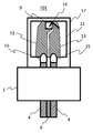
- the TO-CAN type optical semiconductor module 100 includes a stem 1, a lead pin 4 penetrating the stem 1, and a conductor pattern 7 provided on a submount 11 on which the optical semiconductor 9 is mounted, and the lead pin 4 is provided. A gap is provided between the conductor pattern 7 and the conductor pattern 7, and the gap is connected by the brazing filler metal 15.
- FIG. 5 is a cut surface obtained by cutting the TO-CAN type optical semiconductor module 100 along the central axis of the lead pin 4.
- FIG. 5 is a side view of the cut TO-CAN type optical semiconductor module 100.
- the stem 1 has a stem inner surface 1a on the side sealed by the cap 2 and a stem outer surface 1b on the opposite side.
- the stem inner surface 1a is the upper surface of the stem 1
- the stem outer surface 1b is the lower surface of the stem 1.
- the lead pin 4 the portion protruding from the stem inner surface 1a is referred to as an inner lead pin 4a
- the portion protruding from the stem outer surface 1b is referred to as an outer lead pin 4b.
- the impedance of the lead pin 4 is adjusted by the dielectric constant of the sealing material 13 which is a dielectric and the ratio of the through hole diameter to the lead pin 4 diameter.
- the through hole is, for example, a hole having a diameter of 1.0 mm
- the lead pin 4 is, for example, a rod shape having a diameter of 0.38 mm.
- the inner lead pin 4a and the outer lead pin 4b are configured to be as short as possible.
- a feature is that a gap is provided between the top of the inner lead pin 4a and the end of the submount 11 and the gap is connected by the brazing material 15 in order to allow misalignment during assembly.
- the gap may be such that the circular top of the inner lead pin 4a and the conductor pattern 7 of the submount 11 can be connected by using the brazing material 15.
- the brazing material 15 has a gap that can be connected when the brazing material 15 melts to form a hemispherical shape at the top of the inner lead pin 4a. Therefore, the gap is preferably equal to or less than the radius of the top of the circle of the lead pin 4. That is, the gap is preferably less than half the thickness of the lead pin 4.
- the gap is set as a reference position when the sub mount 11 is arranged on the stem 1 to which the lead pin 4 is mounted. Therefore, if the position where the sub mount 11 is arranged is displaced, the gap may disappear as a result.
- the circular top of the inner lead pin 4a can be rephrased as the end point of the lead pin 4.
- the inner lead pin 4a protrudes from the stem inner surface 1a. That is, the end points of the lead pins 4 on the conductor pattern 7 side project from the surface of the stem 1 toward the conductor pattern 7.
- the length of the inner lead pin 4a is preferably 0.05 mm or more in order to suppress interference during assembly of the member. Further, from the viewpoint of high frequency characteristics, the length of the inner lead pin 4a is preferably 1.0 mm or less.
- the circular top of the lead pin 4 is above the stem inner surface 1a, that is, the presence of the inner lead pin 4a allows the sealing material 13 to be filled up to the vicinity of the stem inner surface 1a. As a result, impedance matching of the lead pin 4 can be maintained in the through hole of the stem 1. Further, when the sealing material 13 is sealed to the through hole, the sealing material 13 crawls up to the top of the circle of the lead pin 4 and hinders the electrical connection with the conductor pattern 7 or the brazing material 15. Can be avoided.
- the amount of the sealing material 13 can be increased as compared with the case where the inner lead pin 4a is not present, and the sealing material 13 can be densely filled in the through hole of the stem 1. ..
- the mounted semiconductor element can be protected from dust and moisture in the air, and failure can be suppressed.
- a sufficient sealing material 13 cannot be inserted into the through hole of the stem 1 in order to prevent the lead pin 4 from being buried in the sealing material 13.
- connectivity with the conductor pattern 7 can be ensured as long as the inner lead pin 4a is not covered. Therefore, an error in the encapsulation amount of the encapsulant 13 can be tolerated.
- the lead pin 4 and the conductor pattern 7 of the submount 11 are brazed by utilizing the wettability of the brazing material 15, so that they can be connected even if they are not on the same axis. Therefore, since the conductor pattern 7 is not required on the side surface of the submount 11 on the circular top surface side of the lead pin 4, that is, the side surface metallization is not required, the submount 11 can be manufactured at a relatively low cost.
- FIG. 6 is a cut surface obtained by cutting the TO-CAN type optical semiconductor module 100 on the stem inner surface 1a.
- FIG. 6 is a bottom view of the vicinity of the lead pin 4 of the cut TO-CAN type optical semiconductor module 100.
- the submount 11 includes a conductor pattern 7 on the front surface of the dielectric substrate 18 and a conductor pattern 8 on the back surface of the dielectric substrate 18.
- the submount 11 is connected to and fixed to the support block 17 by the brazing filler metal 16.
- the conductor pattern 8 is provided on the surface that is the back surface of the sub mount 11 on which the conductor pattern 7 is provided.
- the conductor pattern 8 is grounded and becomes a grounding pattern. By providing the conductor pattern 8, the high frequency transmission characteristics are improved.
- the lead pin 4 and the conductor pattern 7 are connected by a brazing material 15.
- the conductor pattern 7 is arranged at a position where the rod-shaped lead pin 4 is extended in the length direction. In FIG. 6 when the lead pin 4 is viewed from below, the cross section of the lead pin 4 and the conductor pattern 7 overlap. As described above, when the conductor pattern 7 is arranged on the extension line of the lead pin 4, the high frequency transmission characteristic is improved. Even if the conductor pattern 7 is not arranged on the extension line of the lead pin 4, the lead pin 4 and the conductor pattern 7 are connected by the brazing material 15. By arranging the conductor pattern 7 at a position where the end surface of the lead pin 4 is extended in the length direction of the lead pin 4, the high frequency transmission characteristic is improved.
- the brazing material 15 between the lead pin 4 and the conductor pattern 7 has a thickness of about the lead pin 4. That is, the brazing material 15 between the lead pin 4 and the conductor pattern 7 has a cross-sectional area equal to or larger than the cross section of the lead pin 4. As a result, the impedance near the inner lead pin 4a and the impedance near the brazing material 15 become the same, so that the high frequency transmission characteristic can be maintained. When the lead pin 4 and the conductor pattern 7 are connected by a bonding wire or the like, the impedance changes and the high frequency transmission characteristic cannot be maintained. In this way, by connecting the lead pin 4 and the conductor pattern 7 with the brazing material 15, it is possible to suppress a decrease in high frequency transmission characteristics.
- the conductor pattern 8 should be grounded over a wide area.
- the brazing filler metal 16 is inserted in a wide range between the submount 11 and the support block 17.
- the area of the surface of the support block 17 in contact with the submount 11 is increased with respect to the area of the conductor pattern 8.
- FIG. 7 is an example of the TO-CAN type optical semiconductor module 100 when the submount 11 is displaced.
- the submount 11 is fixed to the support block 17 in a state of being rotated clockwise. Due to such a misalignment, one of the two conductor patterns 7 shifts upward and the other shifts downward.
- a gap is provided between the lead pin 4 and the sub mount 11, it is possible to prevent a collision between the sub mount 11 and the lead pin 4.
- it can be fixed in a flexible shape by the brazing material 15 which becomes a fluid at the time of welding, it is possible to obtain an electrical connection between the conductor pattern 7 and the lead pin 4 even if there is a misalignment.
- X be the width and Y be the height when the sub mount 11 is viewed from the front.
- D (X / 2) * Sin ⁇ (Y / 2) * (1-Cos ⁇ ).
- X 1.8 mm
- Y 1.2 mm
- ⁇ 1 degree
- the amount of downward misalignment of the lower right corner of the submount 11 when viewed from the front is 0.016 mm.
- it is desirable that the gap is 0.016 mm or more.
- the plurality of lead pins 4 are arranged with a gap between them and the conductor pattern 7, and the gap is connected by the brazing material 15.
- the size of the gap may be determined in consideration of the misalignment of both the lead pin 4 and the sub mount 11. In this case, the maximum values of the respective installation position errors are added together. That is, the distance between the lead pin 4 and the conductor pattern 7 is the sum of the maximum value of the error of the installation position of the lead pin 4 and the maximum value of the error of the installation position of the conductor pattern 7 in the length direction of the lead pin 4. It is as follows.
- the tolerance at the time of assembling the member can be absorbed.
- the brazing material 15 having fluidity at the time of brazing can ensure electrical connectivity and high frequency characteristics. Since it is possible to give a degree of freedom to the mounting position in this way, it is possible to provide the TO-CAN type optical semiconductor module 100 having excellent productivity.
- FIG. 8 is a configuration diagram showing the TO-CAN type optical semiconductor module 101 according to the first modification of the first embodiment.
- FIG. 8 is an explanatory view of the TO-CAN type optical semiconductor module 101 as viewed from the front.
- FIG. 9 is an explanatory view of the TO-CAN type optical semiconductor module 101 as viewed from above.
- the TO-CAN type optical semiconductor module 101 has two lead pins 4 arranged in one through hole with respect to the TO-CAN type optical semiconductor module 100, and omits parts related to the optical semiconductor 10. Since the other components are the same as those in FIGS. 1 to 4, the description thereof will be omitted.
- the TO-CAN type optical semiconductor module 101 includes a stem 1, a lead pin 4, a conductor pattern 7, and a brazing material 15.
- the TO-CAN type optical semiconductor module 101 can include a cap 2, a lens 3, a lead pin 6, an optical semiconductor 9, a submount 11, a sealing material 13, a bonding wire 14, and a support block 17.
- Stem 1 has one through hole. Two lead pins 4 are arranged in the through hole. Then, the sealing material 13 is sealed between the through hole of the stem 1 and the two lead pins 4. The sealing material 13 seals the two lead pins 4 into the through holes of the stem 1 without contacting the stem 1.
- the TO-CAN type optical semiconductor module 101 is provided with a gap between the conductor pattern 7 on the submount 11 and the lead pin 4, and the gap is connected by the brazing material 15. ..
- Stem 1 is, for example, a columnar shape with a diameter of 3.8 mm.
- the through hole of the stem 1 has, for example, a shape in which two holes having a diameter of 1.0 mm are overlapped.
- the through hole of the stem 1 may have a shape in which a conductor does not intervene between the two lead pins 4.
Landscapes
- Physics & Mathematics (AREA)
- Condensed Matter Physics & Semiconductors (AREA)
- General Physics & Mathematics (AREA)
- Electromagnetism (AREA)
- Optics & Photonics (AREA)
- Semiconductor Lasers (AREA)
Priority Applications (2)
| Application Number | Priority Date | Filing Date | Title |
|---|---|---|---|
| JP2020547237A JPWO2021166073A1 (https=) | 2020-02-18 | 2020-02-18 | |
| PCT/JP2020/006307 WO2021166073A1 (ja) | 2020-02-18 | 2020-02-18 | To-can型光半導体モジュール |
Applications Claiming Priority (1)
| Application Number | Priority Date | Filing Date | Title |
|---|---|---|---|
| PCT/JP2020/006307 WO2021166073A1 (ja) | 2020-02-18 | 2020-02-18 | To-can型光半導体モジュール |
Publications (1)
| Publication Number | Publication Date |
|---|---|
| WO2021166073A1 true WO2021166073A1 (ja) | 2021-08-26 |
Family
ID=77390707
Family Applications (1)
| Application Number | Title | Priority Date | Filing Date |
|---|---|---|---|
| PCT/JP2020/006307 Ceased WO2021166073A1 (ja) | 2020-02-18 | 2020-02-18 | To-can型光半導体モジュール |
Country Status (2)
| Country | Link |
|---|---|
| JP (1) | JPWO2021166073A1 (https=) |
| WO (1) | WO2021166073A1 (https=) |
Cited By (1)
| Publication number | Priority date | Publication date | Assignee | Title |
|---|---|---|---|---|
| WO2023109210A1 (zh) * | 2021-12-17 | 2023-06-22 | 青岛海信宽带多媒体技术有限公司 | 光模块 |
Citations (8)
| Publication number | Priority date | Publication date | Assignee | Title |
|---|---|---|---|---|
| US20050105911A1 (en) * | 2003-11-14 | 2005-05-19 | Yong-Chan Keh | TO-can type optical module |
| JP2006216839A (ja) * | 2005-02-04 | 2006-08-17 | Mitsubishi Electric Corp | 光モジュール |
| JP2007150182A (ja) * | 2005-11-30 | 2007-06-14 | Mitsubishi Electric Corp | 光素子用ステムとこれを用いた光半導体装置 |
| JP2009077365A (ja) * | 2007-08-29 | 2009-04-09 | Kyocera Corp | 信号端子と信号線路導体との接続構造および電子部品搭載用パッケージならびに電子装置 |
| JP2009152520A (ja) * | 2007-11-26 | 2009-07-09 | Kyocera Corp | 信号端子と信号線路導体との接続構造および電子部品搭載用パッケージならびに電子装置 |
| JP2011061750A (ja) * | 2009-09-15 | 2011-03-24 | Nippon Telegr & Teleph Corp <Ntt> | 高周波線路の接続方法、構造及び当該構造を有するパッケージ |
| JP2016225457A (ja) * | 2015-05-29 | 2016-12-28 | 新光電気工業株式会社 | 半導体装置用ステム及び半導体装置 |
| WO2019082602A1 (ja) * | 2017-10-26 | 2019-05-02 | 京セラ株式会社 | 接合構造体、半導体パッケージおよび半導体装置 |
Family Cites Families (3)
| Publication number | Priority date | Publication date | Assignee | Title |
|---|---|---|---|---|
| JP2010062512A (ja) * | 2008-07-02 | 2010-03-18 | Kyocera Corp | 電子部品搭載用パッケージおよびそれを用いた電子装置 |
| JP6502797B2 (ja) * | 2015-08-31 | 2019-04-17 | 日本オクラロ株式会社 | 光モジュール |
| JP6929113B2 (ja) * | 2017-04-24 | 2021-09-01 | 日本ルメンタム株式会社 | 光アセンブリ、光モジュール、及び光伝送装置 |
-
2020
- 2020-02-18 WO PCT/JP2020/006307 patent/WO2021166073A1/ja not_active Ceased
- 2020-02-18 JP JP2020547237A patent/JPWO2021166073A1/ja active Pending
Patent Citations (8)
| Publication number | Priority date | Publication date | Assignee | Title |
|---|---|---|---|---|
| US20050105911A1 (en) * | 2003-11-14 | 2005-05-19 | Yong-Chan Keh | TO-can type optical module |
| JP2006216839A (ja) * | 2005-02-04 | 2006-08-17 | Mitsubishi Electric Corp | 光モジュール |
| JP2007150182A (ja) * | 2005-11-30 | 2007-06-14 | Mitsubishi Electric Corp | 光素子用ステムとこれを用いた光半導体装置 |
| JP2009077365A (ja) * | 2007-08-29 | 2009-04-09 | Kyocera Corp | 信号端子と信号線路導体との接続構造および電子部品搭載用パッケージならびに電子装置 |
| JP2009152520A (ja) * | 2007-11-26 | 2009-07-09 | Kyocera Corp | 信号端子と信号線路導体との接続構造および電子部品搭載用パッケージならびに電子装置 |
| JP2011061750A (ja) * | 2009-09-15 | 2011-03-24 | Nippon Telegr & Teleph Corp <Ntt> | 高周波線路の接続方法、構造及び当該構造を有するパッケージ |
| JP2016225457A (ja) * | 2015-05-29 | 2016-12-28 | 新光電気工業株式会社 | 半導体装置用ステム及び半導体装置 |
| WO2019082602A1 (ja) * | 2017-10-26 | 2019-05-02 | 京セラ株式会社 | 接合構造体、半導体パッケージおよび半導体装置 |
Cited By (1)
| Publication number | Priority date | Publication date | Assignee | Title |
|---|---|---|---|---|
| WO2023109210A1 (zh) * | 2021-12-17 | 2023-06-22 | 青岛海信宽带多媒体技术有限公司 | 光模块 |
Also Published As
| Publication number | Publication date |
|---|---|
| JPWO2021166073A1 (https=) | 2021-08-26 |
Similar Documents
| Publication | Publication Date | Title |
|---|---|---|
| JP3998526B2 (ja) | 光半導体用パッケージ | |
| CN102422193B (zh) | 具有陶瓷封装的光学装置的光学组件 | |
| JP6614811B2 (ja) | 半導体装置用ステム及び半導体装置 | |
| US7837398B2 (en) | Optical module having a block with feedthrough pins | |
| US20100020839A1 (en) | Optical device package and optical semiconductor device using the same | |
| US7039083B2 (en) | High speed optical transmission assembly | |
| US11923652B2 (en) | Header for semiconductor package, and semiconductor package | |
| JP4923542B2 (ja) | 光素子用ステムとこれを用いた光半導体装置 | |
| WO2021014568A1 (ja) | To-can型光送信モジュール | |
| JP4212845B2 (ja) | 光半導体素子モジュール | |
| US20120287955A1 (en) | Optical semiconductor element package and optical semiconductor device | |
| KR102777084B1 (ko) | 반도체 장치용 헤더 및 반도체 장치 | |
| CN100592585C (zh) | 光学元件用组件及使用该组件的光学半导体器件 | |
| WO2021166073A1 (ja) | To-can型光半導体モジュール | |
| TWI845854B (zh) | 半導體裝置 | |
| US7192201B2 (en) | Optical transmitting module having a de-coupling inductor therein | |
| JP4105647B2 (ja) | 半導体レーザモジュール及び光伝送器 | |
| JP5153682B2 (ja) | 半導体素子収納用パッケージおよび光半導体装置 | |
| JP5515182B2 (ja) | 光モジュール | |
| US11955403B2 (en) | Header for semiconductor package and semiconductor package | |
| JP7246590B1 (ja) | 半導体レーザ光源装置 | |
| US20240047936A1 (en) | Electronic component package and the manufacturing method thereof | |
| JP7556107B1 (ja) | プラグおよびこれを備えた電子部品収納用パッケージ、電子モジュール | |
| JP7753534B2 (ja) | レーザ装置 | |
| WO2020230327A1 (ja) | 光モジュール |
Legal Events
| Date | Code | Title | Description |
|---|---|---|---|
| ENP | Entry into the national phase |
Ref document number: 2020547237 Country of ref document: JP Kind code of ref document: A |
|
| 121 | Ep: the epo has been informed by wipo that ep was designated in this application |
Ref document number: 20919884 Country of ref document: EP Kind code of ref document: A1 |
|
| NENP | Non-entry into the national phase |
Ref country code: DE |
|
| 122 | Ep: pct application non-entry in european phase |
Ref document number: 20919884 Country of ref document: EP Kind code of ref document: A1 |