WO2021153218A1 - 光電変換素子及びその製造方法 - Google Patents
光電変換素子及びその製造方法 Download PDFInfo
- Publication number
- WO2021153218A1 WO2021153218A1 PCT/JP2021/000699 JP2021000699W WO2021153218A1 WO 2021153218 A1 WO2021153218 A1 WO 2021153218A1 JP 2021000699 W JP2021000699 W JP 2021000699W WO 2021153218 A1 WO2021153218 A1 WO 2021153218A1
- Authority
- WO
- WIPO (PCT)
- Prior art keywords
- photoelectric conversion
- supporting sheet
- conversion element
- layer
- power generation
- Prior art date
- Legal status (The legal status is an assumption and is not a legal conclusion. Google has not performed a legal analysis and makes no representation as to the accuracy of the status listed.)
- Ceased
Links
Images

Classifications
-
- H—ELECTRICITY
- H10—SEMICONDUCTOR DEVICES; ELECTRIC SOLID-STATE DEVICES NOT OTHERWISE PROVIDED FOR
- H10K—ORGANIC ELECTRIC SOLID-STATE DEVICES
- H10K71/00—Manufacture or treatment specially adapted for the organic devices covered by this subclass
- H10K71/10—Deposition of organic active material
- H10K71/12—Deposition of organic active material using liquid deposition, e.g. spin coating
- H10K71/15—Deposition of organic active material using liquid deposition, e.g. spin coating characterised by the solvent used
-
- H—ELECTRICITY
- H10—SEMICONDUCTOR DEVICES; ELECTRIC SOLID-STATE DEVICES NOT OTHERWISE PROVIDED FOR
- H10K—ORGANIC ELECTRIC SOLID-STATE DEVICES
- H10K30/00—Organic devices sensitive to infrared radiation, light, electromagnetic radiation of shorter wavelength or corpuscular radiation
- H10K30/10—Organic devices sensitive to infrared radiation, light, electromagnetic radiation of shorter wavelength or corpuscular radiation comprising heterojunctions between organic semiconductors and inorganic semiconductors
- H10K30/15—Sensitised wide-bandgap semiconductor devices, e.g. dye-sensitised TiO2
- H10K30/151—Sensitised wide-bandgap semiconductor devices, e.g. dye-sensitised TiO2 the wide bandgap semiconductor comprising titanium oxide, e.g. TiO2
-
- H—ELECTRICITY
- H10—SEMICONDUCTOR DEVICES; ELECTRIC SOLID-STATE DEVICES NOT OTHERWISE PROVIDED FOR
- H10K—ORGANIC ELECTRIC SOLID-STATE DEVICES
- H10K30/00—Organic devices sensitive to infrared radiation, light, electromagnetic radiation of shorter wavelength or corpuscular radiation
- H10K30/20—Organic devices sensitive to infrared radiation, light, electromagnetic radiation of shorter wavelength or corpuscular radiation comprising organic-organic junctions, e.g. donor-acceptor junctions
-
- H—ELECTRICITY
- H10—SEMICONDUCTOR DEVICES; ELECTRIC SOLID-STATE DEVICES NOT OTHERWISE PROVIDED FOR
- H10K—ORGANIC ELECTRIC SOLID-STATE DEVICES
- H10K30/00—Organic devices sensitive to infrared radiation, light, electromagnetic radiation of shorter wavelength or corpuscular radiation
- H10K30/40—Organic devices sensitive to infrared radiation, light, electromagnetic radiation of shorter wavelength or corpuscular radiation comprising a p-i-n structure, e.g. having a perovskite absorber between p-type and n-type charge transport layers
-
- H—ELECTRICITY
- H10—SEMICONDUCTOR DEVICES; ELECTRIC SOLID-STATE DEVICES NOT OTHERWISE PROVIDED FOR
- H10K—ORGANIC ELECTRIC SOLID-STATE DEVICES
- H10K30/00—Organic devices sensitive to infrared radiation, light, electromagnetic radiation of shorter wavelength or corpuscular radiation
- H10K30/80—Constructional details
- H10K30/81—Electrodes
-
- H—ELECTRICITY
- H10—SEMICONDUCTOR DEVICES; ELECTRIC SOLID-STATE DEVICES NOT OTHERWISE PROVIDED FOR
- H10K—ORGANIC ELECTRIC SOLID-STATE DEVICES
- H10K71/00—Manufacture or treatment specially adapted for the organic devices covered by this subclass
- H10K71/40—Thermal treatment, e.g. annealing in the presence of a solvent vapour
-
- H—ELECTRICITY
- H10—SEMICONDUCTOR DEVICES; ELECTRIC SOLID-STATE DEVICES NOT OTHERWISE PROVIDED FOR
- H10K—ORGANIC ELECTRIC SOLID-STATE DEVICES
- H10K71/00—Manufacture or treatment specially adapted for the organic devices covered by this subclass
- H10K71/50—Forming devices by joining two substrates together, e.g. lamination techniques
-
- H—ELECTRICITY
- H10—SEMICONDUCTOR DEVICES; ELECTRIC SOLID-STATE DEVICES NOT OTHERWISE PROVIDED FOR
- H10K—ORGANIC ELECTRIC SOLID-STATE DEVICES
- H10K85/00—Organic materials used in the body or electrodes of devices covered by this subclass
- H10K85/20—Carbon compounds, e.g. carbon nanotubes or fullerenes
- H10K85/221—Carbon nanotubes
-
- H—ELECTRICITY
- H10—SEMICONDUCTOR DEVICES; ELECTRIC SOLID-STATE DEVICES NOT OTHERWISE PROVIDED FOR
- H10K—ORGANIC ELECTRIC SOLID-STATE DEVICES
- H10K85/00—Organic materials used in the body or electrodes of devices covered by this subclass
- H10K85/50—Organic perovskites; Hybrid organic-inorganic perovskites [HOIP], e.g. CH3NH3PbI3
-
- H—ELECTRICITY
- H10—SEMICONDUCTOR DEVICES; ELECTRIC SOLID-STATE DEVICES NOT OTHERWISE PROVIDED FOR
- H10K—ORGANIC ELECTRIC SOLID-STATE DEVICES
- H10K30/00—Organic devices sensitive to infrared radiation, light, electromagnetic radiation of shorter wavelength or corpuscular radiation
- H10K30/50—Photovoltaic [PV] devices
-
- Y—GENERAL TAGGING OF NEW TECHNOLOGICAL DEVELOPMENTS; GENERAL TAGGING OF CROSS-SECTIONAL TECHNOLOGIES SPANNING OVER SEVERAL SECTIONS OF THE IPC; TECHNICAL SUBJECTS COVERED BY FORMER USPC CROSS-REFERENCE ART COLLECTIONS [XRACs] AND DIGESTS
- Y02—TECHNOLOGIES OR APPLICATIONS FOR MITIGATION OR ADAPTATION AGAINST CLIMATE CHANGE
- Y02E—REDUCTION OF GREENHOUSE GAS [GHG] EMISSIONS, RELATED TO ENERGY GENERATION, TRANSMISSION OR DISTRIBUTION
- Y02E10/00—Energy generation through renewable energy sources
- Y02E10/50—Photovoltaic [PV] energy
- Y02E10/549—Organic PV cells
-
- Y—GENERAL TAGGING OF NEW TECHNOLOGICAL DEVELOPMENTS; GENERAL TAGGING OF CROSS-SECTIONAL TECHNOLOGIES SPANNING OVER SEVERAL SECTIONS OF THE IPC; TECHNICAL SUBJECTS COVERED BY FORMER USPC CROSS-REFERENCE ART COLLECTIONS [XRACs] AND DIGESTS
- Y02—TECHNOLOGIES OR APPLICATIONS FOR MITIGATION OR ADAPTATION AGAINST CLIMATE CHANGE
- Y02P—CLIMATE CHANGE MITIGATION TECHNOLOGIES IN THE PRODUCTION OR PROCESSING OF GOODS
- Y02P70/00—Climate change mitigation technologies in the production process for final industrial or consumer products
- Y02P70/50—Manufacturing or production processes characterised by the final manufactured product
Definitions
- the present invention relates to a photoelectric conversion element and a method for manufacturing the same.
- Solar cells are attracting attention as photoelectric conversion elements that convert light energy into electric power.
- solar cells for example, a perovskite solar cell using a perovskite compound as a power generation layer.
- perovskite solar cell using a perovskite compound as a power generation layer.
- many studies have been made to improve the photoelectric conversion efficiency of photoelectric conversion elements and solar cells.
- Patent Document 1 a flexible composite self-supporting film containing a fibrous and / or nanotube-like structural material and having flexibility, and a semiconductor layer formed on the surface of the structure-retaining layer.
- a solar cell provided with a composite self-supporting film is proposed.
- Patent Document 2 a solid-state bonding type photoelectric conversion element including a base material, a first conductive layer, and a conductive material including a perovskite layer in this order, and the conductive material is a solid-state bonding having self-supporting property.
- a type photoelectric conversion element has been proposed.
- Non-Patent Document 1 proposes a perovskite solar cell provided with a single-walled carbon nanotube having a thickness of about 100 nm on a perovskite film.
- an object of the present invention is to provide a photoelectric conversion element which exhibits excellent photoelectric conversion efficiency and is easy to manufacture, and a method for manufacturing the photoelectric conversion element.
- the present inventor conducted a diligent study for the purpose of solving the above problems. Then, the present inventor provides the porous self-supporting sheet containing at least a single-walled carbon nanotube on the power generation layer of the photoelectric conversion element, so that the porous self-supporting sheet functions as a hole transport layer and serves as a current collecting electrode. Further, they have found that the obtained photoelectric conversion element exhibits excellent photoelectric conversion efficiency and is easy to manufacture, and completed the present invention.
- the present invention aims to advantageously solve the above problems, and the photoelectric conversion element of the present invention includes a translucent substrate, a transparent conductive film, a first conductive layer, and a power generation layer.
- the photoelectric conversion element is formed by integrating a laminate having a translucent substrate, a transparent conductive film, a first conductive layer, a power generation layer, and a second conductive layer in this order.
- the second conductive layer is made of a porous self-supporting sheet containing at least a single-walled carbon nanotube, it is possible to provide a photoelectric conversion element which exhibits excellent photoelectric conversion efficiency and is easy to manufacture.
- the "porous self-supporting sheet” refers to a sheet in which a plurality of pores are formed and which maintains the shape as a sheet even without a support.
- the porous self-supporting sheet used in the present invention does not cause tearing of the sheet even when the porous self-supporting sheet is immersed in a predetermined solution, pulled up, and then the porous self-supporting sheet is attached to the object to be attached. , The shape as a sheet is maintained.
- porous self-supporting sheet used in the present invention may be used, for example, when chlorobenzene or the like, which is a poor solvent for the perovskite compound, is dropped onto the sheet or handled using a jig used for attaching the sheet. , The sheet does not tear or deform.
- the porous self-supporting sheet used in the present invention preferably retains its shape as a sheet without a support in a size of, for example, a film thickness of 1 ⁇ m to 200 ⁇ m and an area of 1 mm 2 to 100 cm 2.
- a bonding layer is provided at least in a part between the power generation layer and the second conductive layer, and the bonding layer is made of the organic material A, and the power generation layer and the power generation layer and the bonding layer are provided. It may have a composition and properties different from those of the second conductive layer.
- the photoelectric conversion element is formed by integrating a laminate having a translucent substrate, a transparent conductive film, a first conductive layer, a power generation layer, and a second conductive layer in this order.
- the second conductive layer is made of a porous self-supporting sheet containing at least a single-walled carbon nanotube, and has a bonding layer at least a part between the power generation layer and the second conductive layer, and the bonding is performed.
- a photoelectric conversion element that exhibits excellent photoelectric conversion efficiency and is easy to manufacture even if the layer is made of organic material A and has a composition and properties different from those of the power generation layer and the second conductive layer. Can be provided.
- the porous self-supporting sheet may contain the organic material A. If the porous self-supporting sheet contains the organic material A, electric charges are satisfactorily transferred between the power generation layer and the second conductive layer, so that the photoelectric conversion efficiency is enhanced.
- the film thickness of the porous self-supporting sheet is usually 20 ⁇ m or more.
- the function as a current collecting electrode can be sufficiently imparted to the second conductive layer.
- the porous self-supporting sheet may contain at least a part of the material constituting the power generation layer or the material constituting the power generation layer. If the porous self-supporting sheet contains at least a part of the material constituting the power generation layer or the material constituting the power generation layer, the electric charge is satisfactorily transferred between the power generation layer and the second conductive layer. Therefore, the photoelectric conversion efficiency is improved.
- the power generation layer contains a perovskite compound.
- the average diameter (Av) and the standard deviation ( ⁇ ) of the diameter have a relational expression: 0.20 ⁇ (3 ⁇ / Av) ⁇ 0.60. It is preferable to satisfy. If single-walled carbon nanotubes satisfying the above relational expression are used, the photoelectric conversion efficiency can be further improved.
- the "average diameter of carbon nanotubes (Av)” and “standard deviation of the diameter of carbon nanotubes ( ⁇ : standard deviation)” are the diameters of 100 single-walled CNTs randomly selected using a transmission electron microscope, respectively. It can be obtained by measuring (outer diameter).
- the average diameter (Av) and standard deviation ( ⁇ ) of the single-walled CNTs may be adjusted by changing the manufacturing method and manufacturing conditions of the single-walled CNTs, or the single-walled CNTs obtained by different manufacturing methods may be used. It may be adjusted by combining a plurality of types.
- the single-walled carbon nanotubes show an upwardly convex shape in the t-plot obtained from the adsorption isotherm. If a single-walled carbon nanotube whose t-plot shows a convex shape upward is used, a more stable porous self-supporting sheet can be produced, and a photoelectric conversion element can be stably produced.
- the first conductive layer contains a metal oxide and / or an organic compound.
- the performance of the photoelectric conversion element is further improved. be able to.
- the present invention aims to advantageously solve the above problems, and the method for manufacturing a photoelectric conversion element of the present invention is any of the above-mentioned methods for manufacturing a photoelectric conversion element, and the power generation is described. It is characterized by including a step of laminating the porous self-supporting sheet on the power generation layer in a state where at least one joint surface of the layer and the porous self-supporting sheet holds a solvent or a solution.
- the solvent is a poor solvent
- the porous self-supporting sheet impregnated with the solvent may be laminated on the power generation layer. In this way, the porous self-supporting sheet can be satisfactorily attached to the power generation layer.
- the power generation layer is a layer made of a perovskite compound
- the solution is a solution obtained by dissolving at least one precursor of the perobskite compound in a poor solvent.
- the porous self-supporting sheet impregnated with the solution may be laminated on the power generation layer.
- a porous self-supporting sheet containing at least one precursor of the perovskite compound can be laminated on the power generation layer. Therefore, in the obtained photoelectric conversion element, between the power generation layer and the second conductive layer. Charges can be transferred efficiently, and as a result, photoelectric conversion efficiency is improved.
- the solution is an organic material-containing solution obtained by dissolving the organic material A in a poor solvent, and the porous self-supporting sheet impregnated with the organic material-containing solution. May be laminated on the power generation layer. Even in this way, the porous self-supporting sheet can be satisfactorily attached to the power generation layer.
- the method for manufacturing a photoelectric conversion element of the present invention preferably includes a step of heat-pressing the porous self-supporting sheet laminated on the power generation layer. As a result, a photoelectric conversion element having excellent integrity can be obtained.
- the present invention it is possible to provide a photoelectric conversion element that exhibits excellent photoelectric conversion efficiency and is easy to manufacture, and a method for manufacturing the photoelectric conversion element.
- the photoelectric conversion element of the present invention is not particularly limited, and can be used, for example, as a perovskite solar cell.
- an embodiment of the photoelectric conversion element of the present invention and a modification thereof will be described in detail with reference to FIGS. 1 and 2.
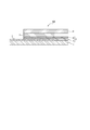
- FIG. 1 is a cross-sectional view schematically showing the configuration of a photoelectric conversion element according to an embodiment of the present invention.
- the photoelectric conversion element 100 includes a translucent substrate 1, a transparent conductive film 2, a first conductive layer 5 composed of a base layer 3 and a porous semiconductor layer 4, a power generation layer 6, and a second conductive layer 8.
- the laminated bodies provided in order are integrated.
- the second conductive layer 8 is made of a porous self-supporting sheet containing at least single-walled carbon nanotubes (hereinafter, referred to as “single-walled CNT”).
- single-walled CNT single-walled carbon nanotubes
- the translucent substrate 1 constitutes the substrate of the photoelectric conversion element 100.
- the translucent substrate 1 is not particularly limited, and examples thereof include a substrate made of glass or a synthetic resin, a film made of a synthetic resin, and the like.
- Examples of the glass constituting the translucent substrate 1 include inorganic glass such as soda glass.
- Examples of the synthetic resin constituting the translucent substrate 1 include polyacrylic resin, polycarbonate resin, polyester resin, polyimide resin, polystyrene resin, polyvinyl chloride resin, polyamide resin, and polycycloolefin resin.
- polyacrylic resin polycarbonate resin
- polyester resin polyimide resin
- polystyrene resin polyvinyl chloride resin
- polyamide resin polyamide resin
- polycycloolefin resin polycycloolefin resin.
- PET polyethylene terephthalate
- PEN polyethylene naphthalate
- the thickness of the translucent substrate 1 is not particularly limited as long as it can maintain the shape of the substrate.
- the thickness of the translucent substrate 1 can be, for example, 0.1 mm or more and 10 mm or less.
- the transparent conductive film 2 is a film made of a metal oxide formed on the surface of the translucent substrate 1. By providing the transparent conductive film 2, conductivity can be imparted to the surface of the translucent substrate 1.
- the metal oxide constituting the transparent conductive film 2 examples include fluorine-doped tin oxide (FTO), tin oxide (SnO), indium oxide (In 2 O 3 ), tin-doped indium oxide (ITO), and zinc oxide (ZnO). , Indium oxide / zinc oxide (IZO), gallium oxide / zinc oxide (GZO) and the like.
- FTO fluorine-doped tin oxide
- SnO tin oxide
- ITO tin-doped indium oxide
- ZnO zinc oxide
- IZO Indium oxide / zinc oxide
- GZO gallium oxide / zinc oxide
- the photoelectric conversion element 100 shown in FIG. 1 the number of transparent conductive films 2 on the translucent substrate 1 is one, but the number of transparent conductive films 2 on the translucent substrate 1 may be two or more. ..
- each transparent conductive film may be composed of the same metal oxide, or may be composed of different metal oxides. You may.
- the film thickness of the transparent conductive film 2 is not particularly limited as long as it can impart desired conductivity to the translucent substrate 1, and can be, for example, 1 nm or more and 1 ⁇ m or less.
- the transparent conductive film 2 may be formed on the entire surface of the translucent substrate 1, or may be formed on a part of the surface of the translucent substrate 1 as shown in FIG.
- the first conductive layer 5 is a layer that functions as a charge transport layer and is composed of an n-type semiconductor.
- the first conductive layer 5 is composed of two layers, a base layer 3 and a porous semiconductor layer 4, but the first conductive layer 5 is an n-type semiconductor. It may be one layer composed of.
- the base layer 3 is an arbitrarily provided layer. By providing the base layer 3, it is possible to prevent the translucent substrate 1 and the transparent conductive film 2 from coming into direct contact with the porous semiconductor layer 4. As a result, the loss of electromotive force is prevented, so that the photoelectric conversion efficiency of the photoelectric conversion element 100 can be improved.
- the base layer 3 may be a porous film or a non-porous dense film as long as it is composed of, for example, an n-type semiconductor, but the translucent substrate 1 and the transparent conductive film may be used. From the viewpoint of sufficiently preventing the 2 from coming into contact with the porous semiconductor layer 4, the base layer 3 is preferably a non-porous dense film.
- the thickness of the base layer 3 is not particularly limited, and can be, for example, 1 nm or more and 500 nm or less. Further, the base layer 3 may optionally contain an insulator material other than the n-type semiconductor at a ratio that does not impair the properties of the base layer 3 as an n-type semiconductor.
- the porous semiconductor layer 4 is a porous layer. By including the porous semiconductor layer 4 in the first conductive layer 5, the photoelectric conversion efficiency of the photoelectric conversion element 100 can be further improved.
- the porous semiconductor layer 4 preferably contains a metal oxide and / or an organic compound, more preferably contains fine particles composed of a metal oxide and / or an organic compound, and fine particles composed of a metal oxide and / or an organic compound. It is more preferably formed from.
- the metal oxide forming the porous semiconductor layer 4 is not particularly limited as long as it functions as an n-type semiconductor, and examples thereof include titanium oxide (TiO 2 ).
- examples of the organic compound forming the porous semiconductor layer 4 include fullerene derivatives such as phenyl C61 butyric acid methyl ester (PCBM).
- PCBM phenyl C61 butyric acid methyl ester
- the particle size (average particle size of the primary particles) of the fine particles of the metal oxide and / or the organic compound used in the porous semiconductor layer 4 is preferably 2 nm or more and 80 nm or less, and more preferably 30 nm or less. Since the particle size is small, the resistance of the porous semiconductor layer 4 can be reduced. As the fine particles, those having the same particle size may be used alone, or those having different particle sizes may be used in combination.
- the average particle size of the fine particles can be determined by measuring the particle size of 100 randomly selected fine particles using an electron microscope.
- the thickness of the porous semiconductor layer 4 is not particularly limited, but is usually 5 nm or more, preferably 10 nm or more, and usually 500 nm or less, preferably 100 nm or less. As shown in FIG. 1, the porous semiconductor layer 4 may be formed from one layer or may be formed from a plurality of layers.
- the power generation layer 6 is a layer composed of a material that generates an electromotive force by absorbing light, preferably a layer containing a perovskite compound, and more preferably a layer composed of a perovskite compound (perovskite layer). be.
- the perovskite compound constituting the power generation layer 6 is not particularly limited, and a known perovskite compound can be used.
- the thickness of the power generation layer 6 is not particularly limited, but is preferably 100 nm or more, more preferably 200 nm or more, preferably 1 ⁇ m or less, and more preferably 800 nm or less. By setting the thickness of the power generation layer 6 to 100 nm or more, the electromotive force of the power generation layer 6 can be increased.
- the second conductive layer 8 is a layer made of a porous self-supporting sheet.
- the porous self-supporting sheet needs to contain at least a single-walled CNT, and is preferably a sheet made of single-walled CNTs, and more preferably a sheet made of buckypaper.
- the second conductive layer 8 can be provided with an excellent function as a hole transport layer and a function as a current collecting electrode.
- Porous self-supporting sheet preferably include single-walled CNTs having the following properties.
- the single-layer CNT contained in the porous self-supporting sheet has a ratio (3 ⁇ / Av) of a value (3 ⁇ ) obtained by multiplying the standard deviation ( ⁇ ) of the diameter by 3 to the average diameter (Av) of more than 0.20. It is preferably more than 0.25, more preferably more than 0.50, and more preferably less than 0.60.
- 3 ⁇ / Av is more than 0.20 and less than 0.60, even if the amount of single-walled CNTs contained in the porous self-supporting sheet is small, it can be used as a sufficient hole transport layer with respect to the second conductive layer 8. It is possible to impart a function and a function as a current collecting electrode.
- the average diameter (Av) of the single-walled CNT is preferably 0.5 nm or more, more preferably 1 nm or more, preferably 15 nm or less, and more preferably 10 nm or less.
- the average diameter (Av) of the single-walled CNTs is 0.5 nm or more, the aggregation of the single-walled CNTs can be suppressed and the dispersibility of the single-walled CNTs in the second conductive layer 8 can be enhanced.
- the average diameter (Av) of the single-walled CNT is 15 nm or less, the second conductive layer 8 can sufficiently exhibit the function as a current collecting electrode.
- the t-plot obtained from the adsorption isotherm shows an upwardly convex shape.
- the single-walled CNT it is more preferable that the single-walled CNT is not subjected to the opening treatment. If a single-walled CNT whose t-plot obtained from the adsorption curve is convex upward is used, the second conductive layer 8 having excellent strength can be obtained.
- the bending point of the t-plot of the single-walled CNT is preferably in the range of 0.2 ⁇ t (nm) ⁇ 1.5, and is in the range of 0.45 ⁇ t (nm) ⁇ 1.5. More preferably, it is more preferably in the range of 0.55 ⁇ t (nm) ⁇ 1.0.
- the single-walled CNT having the above-mentioned properties is not particularly limited, and for example, in the super growth method (see International Publication No. 2006/011655), the efficiency is achieved by forming a catalyst layer on the surface of the base material by a wet process. Can be manufactured as a target.
- the super growth method is a method of synthesizing CNTs by a chemical vapor deposition method (CVD method) by supplying a raw material compound and a carrier gas onto a substrate having a catalyst layer for CNT production on the surface.
- CVD method chemical vapor deposition method
- it is a method of dramatically improving the catalytic activity of the catalyst layer by allowing a trace amount of oxidizing agent (catalyst activator) to be present in the system.
- oxidizing agent catalyst activator
- the porous self-supporting sheet may contain a part of the material constituting the power generation layer 6 described above or a part of the material constituting the power generation layer 6. More specifically, the porous self-supporting sheet may contain a material constituting the power generation layer 6 or a part of the material constituting the power generation layer inside a plurality of pores of the porous self-supporting sheet.
- the ratio of the single-walled CNTs contained in the porous self-supporting sheet is not particularly limited, but is preferably 50% by mass or more, and preferably 75% by mass or more.
- Examples of materials other than single-walled CNTs that can be optionally contained in the porous self-supporting sheet include organic materials and inorganic materials as p-type semiconductors, and fibrous carbon nanostructures other than single-walled CNTs.
- examples of the organic material that can be contained in the porous self-supporting sheet include 2,2', 7,7'-tetrakis (N, N-di-p-methoxyphenylamino) -9,9'-spiro.
- examples thereof include bifluorene (spiro-MeOTAD), poly (3-hexylthiophene) (P3HT), polytriallylamine (PTAA) and the like.
- the inorganic materials which may be contained in the porous self-supporting sheet e.g., CuI, CuSCN, CuO, etc. Cu 2 O and the like.
- the film thickness of the porous self-supporting sheet is usually preferably 20 ⁇ m or more, preferably 30 ⁇ m or more, preferably 200 ⁇ m or less, and more preferably 80 ⁇ m or less.
- the second conductive layer 8 can exhibit a more excellent function as a current collecting electrode.
- the method for producing the porous self-supporting sheet is not particularly limited, and for example, the solvent is removed from the fibrous carbon nanostructure dispersion liquid containing at least a single-walled CNT, a dispersant, and a solvent. Then, a method including a step of forming a porous self-supporting sheet (deposition step) can be adopted. Further, in the method for producing a porous self-supporting sheet, optionally, before the film forming step, a coarse dispersion liquid containing at least a fibrous carbon nanostructure containing a single-walled CNT, a dispersant, and a solvent is dispersed. The step of preparing the fibrous carbon nanostructure dispersion liquid (dispersion liquid preparation step) may be included.
- the crude dispersion liquid containing at least a fibrous carbon nanostructure containing a single-walled CNT, a dispersant, and a solvent is not particularly limited, but a cavitation effect or a crushing effect described later can be obtained in detail. It is preferable to disperse the fibrous carbon nanostructures containing the single-walled CNTs to prepare a fibrous carbon nanostructure dispersion liquid for the dispersion treatment. By performing the dispersion treatment for obtaining the cavitation effect or the crushing effect in this way, a fibrous carbon nanostructure dispersion liquid in which the fibrous carbon nanostructures containing the single-walled CNTs are well dispersed can be obtained.
- the fibrous carbon nanostructure dispersion used for producing the porous self-supporting sheet is prepared by dispersing the fibrous carbon nanostructures containing single-walled CNTs in a solvent using a known dispersion treatment other than the above. You may.
- the fibrous carbon nanostructures used for preparing the fibrous carbon nanostructure dispersion may contain at least single-walled CNTs, for example, single-walled CNTs and fibrous carbon nanostructures other than single-walled CNTs. It may be a mixture with (for example, multi-walled CNT).
- the fibrous carbon nanostructure dispersion liquid has a content ratio of single-walled CNTs and fibrous carbon nanostructures other than single-walled CNTs, for example, a mass ratio (fibrous form other than single-walled CNTs / single-walled CNTs). It can be 50/50 to 75/25 with carbon nanostructures).
- Dispersant The dispersant used for preparing the fibrous carbon nanostructure dispersion can disperse the fibrous carbon nanostructure containing at least a single-walled CNT, and can be dissolved in the solvent used for preparing the fibrous carbon nanostructure dispersion. If so, there is no particular limitation.
- a dispersant for example, a surfactant, a synthetic polymer or a natural polymer can be used.
- surfactant examples include sodium dodecylsulfonate, sodium deoxycholate, sodium cholic acid, sodium dodecylbenzenesulfonate and the like.
- synthetic polymer examples include polyether diol, polyester diol, polycarbonate diol, polyvinyl alcohol, partially saponified polyvinyl alcohol, acetoacetyl group-modified polyvinyl alcohol, acetal group-modified polyvinyl alcohol, butyral group-modified polyvinyl alcohol, and silanol group-modified.
- Polyvinyl alcohol ethylene-vinyl alcohol copolymer, ethylene-vinyl alcohol-vinyl acetate copolymer resin, dimethylaminoethyl acrylate, dimethylaminoethyl methacrylate, acrylic resin, epoxy resin, modified epoxy resin, phenoxy resin, modified phenoxy Examples thereof include resins, phenoxy ether resins, phenoxy ester resins, fluororesins, melamine resins, alkyd resins, phenol resins, polyacrylamides, polyacrylic acids, polystyrene sulfonic acids, polyethylene glycols, polyvinylpyrrolidone and the like.
- natural polymers for example, polysaccharides such as starch, pullulan, dextran, dextrin, guar gum, xanthan gum, amylose, amylopectin, alginic acid, arabic gum, carrageenan, chondroitin sulfate, hyaluronic acid, curdlan, chitin, chitosan, etc.
- polysaccharides such as starch, pullulan, dextran, dextrin, guar gum, xanthan gum, amylose, amylopectin, alginic acid, arabic gum, carrageenan, chondroitin sulfate, hyaluronic acid, curdlan, chitin, chitosan, etc.
- examples include cellulose and salts or derivatives thereof.
- the derivative means a conventionally known compound such as an ester or an ether.
- dispersants can be used alone or in admixture of two or more.
- a surfactant is preferable, and sodium deoxycholate and the like are more preferable, because the fibrous carbon nanostructure containing the single-walled CNT is excellent in dispersibility.
- Solvent The solvent of the fibrous carbon nanostructure dispersion is not particularly limited, and for example, water, methanol, ethanol, n-propanol, isopropanol, n-butanol, isobutanol, t-butanol, pentanol, hexanol, etc.
- Alcohols such as heptanol, octanol, nonanol, decanol, amyl alcohol, ketones such as acetone, methyl ethyl ketone and cyclohexanone, esters such as ethyl acetate and butyl acetate, ethers such as diethyl ether, dioxane and tetrahydrofuran, N, N- Examples thereof include amide-based polar organic solvents such as dimethylformamide and N-methylpyrrolidone, and aromatic hydrocarbons such as toluene, xylene, chlorobenzene, orthodichlorobenzene and paradichlorobenzene. Only one type of these may be used alone, or two or more types may be used in combination.
- the dispersion liquid preparation step it is preferable to perform a dispersion treatment that can obtain, for example, the cavitation effect or the crushing effect shown below.
- the dispersion treatment that obtains the cavitation effect is a dispersion method that utilizes a shock wave caused by the bursting of vacuum bubbles generated in water when high energy is applied to the liquid.
- dispersion treatment that can obtain the cavitation effect
- specific examples of the dispersion treatment that can obtain the cavitation effect include the dispersion treatment by ultrasonic waves, the dispersion treatment by a jet mill, and the dispersion treatment by high shear stirring. Only one of these distributed processes may be performed, or a plurality of distributed processes may be combined. More specifically, for example, an ultrasonic homogenizer, a jet mill and a high shear agitator are preferably used. As these devices, conventionally known devices may be used.
- the crude dispersion may be irradiated with ultrasonic waves by the ultrasonic homogenizer.
- the irradiation time may be appropriately set depending on the amount of single-walled CNTs and the like. For example, 3 minutes or more is preferable, 30 minutes or more is more preferable, 5 hours or less is preferable, and 2 hours or less is more preferable.
- the output is preferably 20 W or more and 500 W or less, more preferably 100 W or more and 500 W or less, and the temperature is preferably 15 ° C. or more and 50 ° C. or less.
- the number of treatments may be appropriately set depending on the amount of single-walled CNTs and the like. For example, 2 times or more is preferable, 5 times or more is more preferable, 100 times or less is preferable, and 50 times or less is preferable. More preferred. Further, for example, the pressure is preferably 20 MPa or more and 250 MPa or less, and the temperature is preferably 15 ° C. or more and 50 ° C. or less.
- stirring and shearing may be added to the crude dispersion liquid by a high shear stirring device.
- the operating time (the time during which the machine is rotating) is preferably 3 minutes or more and 4 hours or less
- the peripheral speed is preferably 5 m / sec or more and 50 m / sec or less
- the temperature is preferably 15 ° C. or more and 50 ° C. or less.
- the dispersion treatment for obtaining the above-mentioned cavitation effect is performed at a temperature of 50 ° C. or lower. This is because the change in concentration due to the volatilization of the solvent is suppressed.
- the dispersion treatment that obtains the crushing effect not only allows the single-walled CNTs to be uniformly dispersed in the solvent, but also causes damage to the single-walled CNTs due to the shock wave when the bubbles disappear, as compared with the dispersion treatment that obtains the above-mentioned cavitation effect. It is more advantageous in that it can be suppressed.
- a shearing force is applied to the coarse dispersion liquid to crush and disperse aggregates of fibrous carbon nanostructures containing single-walled CNTs, and a back pressure is further applied to the coarse dispersion liquid.
- the crude dispersion liquid can be cooled to uniformly disperse the single-walled CNTs in the solvent while suppressing the generation of bubbles.
- the back pressure applied to the crude dispersion liquid may be lowered to atmospheric pressure at once, but it is preferable to lower the pressure in multiple steps.
- the solvent is removed from the fibrous carbon nanostructure dispersion liquid described above to form a porous self-supporting sheet.
- one of the following methods (A) and (B) is used to remove the solvent from the fibrous carbon nanostructure dispersion liquid to form a porous self-supporting sheet. ..
- B A method of filtering a fibrous carbon nanostructure dispersion using a porous film-forming base material and drying the obtained filtered product.
- the film-forming base material is not particularly limited, and a known base material can be used.
- examples of the film-forming base material to which the fibrous carbon nanostructure dispersion liquid is applied in the above method (A) include a resin base material and a glass base material.
- the resin base material polyethylene terephthalate (PET), polyethylene naphthalate (PEN), polytetrafluoroethylene (PTFE), polyimide, polyphenylene sulfide, aramid, polypropylene, polyethylene, polylactic acid, polyvinyl chloride, polycarbonate, etc.
- Examples thereof include a base material made of polymethyl methacrylate, an alicyclic acrylic resin, a cycloolefin resin, triacetyl cellulose and the like.
- a base material made of ordinary soda glass can be mentioned.
- examples of the film-forming base material for filtering the fibrous carbon nanostructure dispersion liquid in the above method (B) include filter paper and a porous sheet made of cellulose, nitrocellulose, alumina and the like.
- a known coating method can be adopted. Specifically, as the coating method, a dipping method, a roll coating method, a gravure coating method, a knife coating method, an air knife coating method, a roll knife coating method, a die coating method, a screen printing method, a spray coating method, a gravure offset method, etc. are used. Can be used.
- a known filtration method As a method of filtering the fibrous carbon nanostructure dispersion liquid using the film-forming base material in the above method (B), a known filtration method can be adopted. Specifically, as the filtration method, natural filtration, vacuum filtration, pressure filtration, centrifugal filtration and the like can be used.
- [Dry] As a method for drying the fibrous carbon nanostructure dispersion applied on the film-forming substrate in the above method (A) or the filtrate obtained in the above method (B), a known drying method can be adopted. Examples of the drying method include a hot air drying method, a vacuum drying method, a hot roll drying method, and an infrared irradiation method.
- the drying temperature is not particularly limited, but is usually room temperature to 200 ° C.
- the drying time is not particularly limited, but is usually 0.1 to 150 minutes.
- the porous self-supporting sheet formed as described above is usually contained in a single-walled CNT, a fibrous carbon nanostructure other than the single-walled CNT, and a fibrous carbon nanostructure dispersion such as a dispersant. It contains the same components as the fibrous carbon nanostructure dispersion. Therefore, in the method for producing the porous self-supporting sheet, the dispersant may be arbitrarily removed from the porous self-supporting sheet by washing the porous self-supporting sheet formed in the film forming step. If the dispersant is removed from the porous self-supporting sheet, the properties such as conductivity of the porous self-supporting sheet can be further enhanced.
- the cleaning of the porous self-supporting sheet can be performed by bringing the dispersant into contact with a soluble solvent and eluting the dispersant in the porous self-supporting sheet into the solvent.
- the solvent capable of dissolving the dispersant in the porous self-supporting sheet is not particularly limited, and the above-mentioned solvent which can be used as a solvent for the fibrous carbon nanostructure dispersion liquid, preferably the fibrous carbon nanostructure.
- the same solvent as the body dispersion can be used.
- the contact between the porous self-supporting sheet and the solvent can be performed by immersing the porous self-supporting sheet in the solvent or applying the solvent to the porous self-supporting sheet.
- the washed porous self-supporting sheet can be dried using known methods.
- the voids may be adjusted as necessary, such as by pressing the porous self-supporting sheet formed in the film forming step to further increase the density. ..
- the press pressure during press working is preferably less than 3 MPa, and it is more preferable not to perform press working.
- the function as a hole transport layer and the function as a current collector electrode can be fulfilled by one second conductive layer 8.
- the second conductive layer 8 is composed of a porous self-supporting sheet containing at least a single-walled CNT, its shape is stable. Therefore, according to such a configuration, it is possible to easily realize a large area of the photoelectric conversion element.
- the photoelectric conversion element of the present invention is an integral body of a laminated body in which the order of each of the above-mentioned constituent members is maintained, and as long as the second conductive layer is made of a porous self-supporting sheet containing at least a single-walled CNT. Other layers and the like may be further provided as long as the effects of the present invention are not impaired.
- the method for manufacturing the photoelectric conversion element 100 of the present invention includes a step of laminating the porous self-supporting sheet on the power generation layer 6 in a state where at least one of the bonding surfaces of the power generation layer 6 and the porous self-supporting sheet holds a solvent or a solution. It is necessary to optionally include a step of heating and pressing the porous self-supporting sheet laminated on the power generation layer 6.
- the above-mentioned “joint surface” refers to the surface on the side where the power generation layer 6 and the porous self-supporting sheet correspond to each other.
- a method for manufacturing the photoelectric conversion element 100 will be specifically described.
- the translucent substrate 1 is prepared.
- the types of the translucent substrate 1 the ones listed in the section of "photoelectric conversion element" can be used.
- the transparent conductive film 2 is formed on the translucent substrate 1.
- the method for forming the transparent conductive film 2 is not particularly limited, and for example, a known method such as a sputtering method or a vapor deposition method can be adopted. By using a commercially available translucent substrate having a transparent conductive film formed on the surface, the formation of the transparent conductive film 2 may be omitted.
- the first conductive layer 5 is formed on the transparent conductive film 2.
- the first conductive layer 5 is obtained by forming a base layer 3 on the transparent conductive film 2 and then forming a porous semiconductor layer 4.
- the method for forming the base layer 3 is not particularly limited, and for example, it can be formed by spraying a solution containing a material for forming an n-type semiconductor onto the transparent conductive film 2.
- examples of the spraying method include a spray pyrolysis method, an aerosol deposition method, an electrostatic spray method, and a cold spray method.
- the method for forming the porous semiconductor layer 4 is not particularly limited, and for example, it can be formed by applying a solution containing a precursor of an n-type semiconductor onto the base layer 3 by a spin coating method or the like and drying it. ..
- examples of the precursor of the n-type semiconductor include titanium alkoxides such as titanium tetrachloride (TiCl 4 ), peroxotitanic acid (PTA), titanium ethoxyoxide, and titanium isopropoxide (TTIP); zinc alkoxide and alkoxysilane.
- titanium alkoxides such as titanium tetrachloride (TiCl 4 ), peroxotitanic acid (PTA), titanium ethoxyoxide, and titanium isopropoxide (TTIP); zinc alkoxide and alkoxysilane.
- TiCl 4 titanium tetrachloride
- PTA peroxotitanic acid
- TTIP titanium isopropoxide
- zinc alkoxide and alkoxysilane titanium alkoxides
- titanium diisopropoxide bis acetylacetonate
- the solvent used for the solution containing the precursor of the n-type semiconductor is not particularly limited, and for example, an alcohol solution such as ethanol can be used.
- the temperature and time for drying the solution applied on the base layer 3 are not particularly limited, and may be appropriately adjusted depending on the type of n-type precursor to be used, the type of solvent, and the like.
- the method for forming the power generation layer 6 includes a vacuum deposition method and a coating method, but is not particularly limited.
- a precursor-containing solution containing a precursor of a perovskite compound is coated on the first conductive layer 5. It can be formed by firing.
- the precursor of the perovskite compound include lead iodide (PbI 2 ) and methyl ammonium iodide (CH 3 NH 3 I).
- the solvent contained in the precursor-containing solution is not particularly limited, and for example, N, N-dimethylformamide, dimethyl sulfoxide, or the like can be used.
- the term “poor solvent” refers to a solvent in which the perovskite compound does not substantially change in the production process. In the manufacturing process, it can be said that the perovskite compound does not substantially change unless the appearance of the perovskite compound is changed by visual observation such as turbidity of the film.
- the concentration of the precursor of the perovskite compound in the precursor-containing solution may be appropriately set to an appropriate concentration depending on the solubility of the material constituting the perovskite compound and the like, and is, for example, about 0.5 M to 1.5 M. Can be done.
- the method of applying the precursor-containing solution onto the first conductive layer 5 is not particularly limited, and for example, a known coating method such as a spin coating method, a spray method, or a bar coating method can be adopted. ..
- the second conductive layer 8 is formed on the power generation layer 6.
- the porous self-supporting sheet is laminated on the power generation layer 6 with at least one bonding surface of the power generation layer 6 and the porous self-supporting sheet holding a solvent or a solution. As a result, the photoelectric conversion element 100 having excellent photoelectric conversion efficiency can be easily manufactured.
- the solvent examples include poor solvents such as chlorobenzene, toluene, and anisole.
- poor solvents such as chlorobenzene, toluene, and anisole.
- the power generation layer 6 is a perovskite layer
- a solution obtained by dissolving at least one precursor of the perovskite compound in a poor solvent can be used as the above solution.
- electric charges can be efficiently transferred between the power generation layer 6 and the second conductive layer 8, and as a result, the photoelectric conversion efficiency can be improved.
- the porous self-supporting sheet impregnated with the solvent or solution described above is used, the solvent or solution can be satisfactorily retained at at least one joint surface of the power generation layer 6 and the porous self-supporting sheet.
- the porous self-supporting sheet impregnated with the solvent or solution can be obtained, for example, by immersing the porous self-supporting sheet in the above-mentioned solvent or solution and then pulling it up.
- the immersion time is not particularly limited, and may be appropriately set according to the solvent to be used, the type of solution, and the like.
- the heating temperature is not particularly limited and can be, for example, about 100 ° C.
- the pressure at the time of heat pressing is not particularly limited, and can be, for example, 0.05 MPa.
- the pressing time is not particularly limited and may be, for example, 30 seconds.
- a member having voids such as a thick wipe, a porous rubber, a porous metal, and a porous ceramic.
- the photoelectric conversion element 100 shown in FIG. 1 can be efficiently manufactured.
- the method for manufacturing the photoelectric conversion element of the present invention is not limited to the above-mentioned method, and may include steps other than the above-mentioned steps as long as the effects of the present invention are not impaired.
- FIG. 2 is a cross-sectional view schematically showing the configuration of a photoelectric conversion element according to a modified example of the embodiment of the present invention.
- the photoelectric conversion element 200 includes a translucent substrate 1, a transparent conductive film 2, a first conductive layer 5 composed of a base layer 3 and a porous semiconductor layer 4, a power generation layer 6, a bonding layer 7, and a second conductive layer.
- a laminate having layers 8 in this order is integrated.
- the bonding layer 7 may be provided in at least a part between the power generation layer 6 and the second conductive layer 8, and as shown in FIG. 2, between the power generation layer 6 and the second conductive layer 8. It may be provided throughout.
- the bonding layer 7 is made of the organic material A and has a composition and properties different from those of the power generation layer 6 and the second conductive layer 8.
- the photoelectric conversion element according to the embodiment of the present invention is the same as the photoelectric conversion element according to the embodiment of the present invention, except that the bonding layer 7 is further provided. Therefore, in the following description, parts having the same basic functions as those in the above-described embodiment are designated by the same reference numerals and the description thereof will be omitted.
- the bonding layer 7 is provided in at least a part between the power generation layer 6 and the second conductive layer 8. Further, the bonding layer 7 is made of the organic material A and has a composition and properties different from those of the power generation layer 6 and the second conductive layer 8. The bonding layer 7 is provided for filling the voids formed between the power generation layer 6 and the second conductive layer 8 by the unevenness of the surface of the power generation layer 6 and the porous self-supporting sheet constituting the second conductive layer 8. Has been done. By providing the bonding layer 7, electric charges are satisfactorily transferred between the power generation layer 6 and the second conductive layer 8 in the photoelectric conversion element 200, so that the photoelectric conversion element 200 exhibits excellent photoelectric conversion efficiency.
- Examples of the organic material A constituting the bonding layer 7 include a polymer material exhibiting adhesiveness such as polymethyl methacrylate (PMMA), 2,2', 7,7'-tetrakis (N, N-di-). Examples thereof include polymer materials exhibiting semiconductor physical characteristics such as p-methoxyphenylamino) -9,9'-spiro-meOTAD. Further, it may be formed by mixing these various materials.
- PMMA polymethyl methacrylate
- N, N-di- 2,2', 7,7'-tetrakis
- Examples thereof include polymer materials exhibiting semiconductor physical characteristics such as p-methoxyphenylamino) -9,9'-spiro-meOTAD. Further, it may be formed by mixing these various materials.
- the thickness of the bonding layer 7 is not particularly limited as long as the gap formed between the power generation layer 6 and the second conductive layer 8 can be filled, and the thickness of the surface of the power generation layer 6 and the second conductive layer 8 is not particularly limited. It can be set as appropriate depending on the shape and the like.
- the porous self-supporting sheet contains the material constituting the above-mentioned bonding layer 7. More specifically, it is preferable that the porous self-supporting sheet contains the organic material A constituting the bonding layer 7 inside a plurality of pores of the porous self-supporting sheet.
- the function as a hole transport layer and the function as a current collector electrode can be fulfilled by one of the second conductive layers 8. Further, by providing the bonding layer 7 between the power generation layer 6 and the second conductive layer 8, the gap between the power generation layer 6 and the second conductive layer 8 is filled, so that the power generation layer 6 and the second conductive layer 8 are filled. The transfer of electric charge to and from No. 8 is performed well, and as a result, the photoelectric conversion efficiency is increased. Further, since the second conductive layer 8 is composed of a porous self-supporting sheet containing at least a single-walled CNT, its shape is stable.
- the photoelectric conversion element of this modification is an integrated product of a laminated body in which the order of each of the above-mentioned constituent members is maintained, and the second conductive layer is made of a porous self-supporting sheet containing at least a single-walled CNT, and is a power generation layer.
- the bonding layer is provided in at least a part of the second conductive layer and the bonding layer is made of the organic material A and has a composition and properties different from those of the power generation layer and the second conductive layer.
- Other layers and the like may be further provided as long as the effect is not impaired.
- the porous self-supporting sheet is laminated on the power generation layer 6 in a state where at least one of the bonding surfaces of the power generation layer 6 and the porous self-supporting sheet holds a solvent or a solution.
- a step of heating and pressing the porous self-supporting sheet laminated on the power generation layer 6 is optionally included.
- a method for manufacturing the photoelectric conversion element 200 will be specifically described.
- the translucent substrate 1 is prepared, the transparent conductive film 2 is formed, and the first conductive layer 5 is formed (formation of the base layer 3 and the porous semiconductor layer 4). , The power generation layer 6, the bonding layer 7, and the second conductive layer 8 are formed.
- the methods for preparing the translucent substrate 1, forming the transparent conductive film 2, forming the first conductive layer 5, forming the base layer 3, forming the porous semiconductor layer 4, and forming the power generation layer 6 are as described above.
- optical substrate 1> Preparation of optical substrate 1>, ⁇ Formation of transparent conductive film 2>, ⁇ Formation of first conductive layer 5> ([Formation of base layer 3], [Formation of porous semiconductor layer 4]), ⁇ Power generation layer 6 Since it is as described in the section of>, the description here is not repeated, and only the method of forming the bonding layer 7 and the second conductive layer 8 will be described below.
- the second conductive layer 8 is formed on the power generation layer 6 via the bonding layer 7.
- the porous self-supporting sheet is attached to the power generation layer 6 in a state where at least one of the bonding surfaces of the power generation layer 6 and the porous self-supporting sheet holds a solvent or a solution. Laminate. As a result, the photoelectric conversion element 200 having excellent photoelectric conversion efficiency can be easily manufactured.
- Examples of the solvent include the solvents mentioned in the section ⁇ Formation of the second conductive layer 8>.
- examples of the above solution include an organic material-containing solution obtained by dissolving the organic material A constituting the above-mentioned bonding layer 7 in a poor solvent.
- the porous self-supporting sheet impregnated with the solvent or solution described above is used, the solvent or solution can be satisfactorily retained at at least one joint surface of the power generation layer 6 and the porous self-supporting sheet.
- the porous self-supporting sheet impregnated with the solvent or solution can be obtained, for example, by immersing the porous self-supporting sheet in the above-mentioned solvent or solution and then pulling it up.
- the immersion time is not particularly limited, and may be appropriately set according to the solvent to be used, the type of solution, and the like.
- the method for forming the bonding layer 7 is not particularly limited, but from the viewpoint of efficiently manufacturing the photoelectric conversion element 200, the organic material A (for example, PMMA described above) constituting the bonding layer 7 is dissolved in a poor solvent.
- the organic material A for example, PMMA described above
- a bonding layer 7 is formed on the porous self-supporting sheet, and then the porous self-supporting sheet is passed through the bonding layer 7. It is preferable to attach it to the power generation layer 6.
- the immersion time, the heating temperature, and the drying time are not particularly limited, and may be appropriately set according to the type of the organic material-containing solution to be used.
- the solvent for dissolving the organic material A constituting the bonding layer it is preferable to use a poor solvent in order to prevent the influence of residue, but if it can be dried without affecting the power generation layer 6, it may be a poor solvent. Not limited to various solvents can be used.
- the method for manufacturing the photoelectric conversion element 200 according to the modified example of the present invention it is preferable to heat-press the porous self-supporting sheet laminated on the power generation layer 6. As a result, the photoelectric conversion element 200 having excellent integrity can be obtained.
- the heating time, the pressure at the time of heating and pressing, the pressing time, and the like are not particularly limited, and can be the same as the heating and pressing conditions described in the method for manufacturing the photoelectric conversion element 100.
- the photoelectric conversion element 200 shown in FIG. 2 can be efficiently manufactured.
- the method for manufacturing the modified photoelectric conversion element of the present invention is not limited to the above-mentioned method, and may include steps other than the above-mentioned steps as long as the effects of the present invention are not impaired.
- the present invention will be specifically described based on examples, but the present invention is not limited to these examples.
- the penetration of the perovskite layer into the pores of the porous self-supporting sheet and the battery performance of the produced perovskite solar cell were measured by using the following methods.
- the perovskite layer digs into the pores of the porous self-supporting sheet>
- the infiltration of the perovskite layer into the pores of the porous self-supporting sheet was observed by the surface condition of the porous self-supporting sheet when the porous self-supporting sheet attached to the perovskite layer was peeled off. Then, by microscopic observation, if irregularities were formed on the entire surface of the perovskite layer in contact with the porous self-supporting sheet, the perovskite layer was "presenced” into the pores of the porous self-supporting sheet. Further, if the entire surface of the perovskite layer in contact with the porous self-supporting sheet was not formed with irregularities, the perovskite layer was "none" embedded in the pores of the porous self-supporting sheet.
- a pseudo-solar irradiation device (PEC-L11 type, manufactured by Pexel Technologies Co., Ltd.) in which an AM1.5G filter was attached to a 150 W xenon lamp light source was used.
- the light source was adjusted to 1 sun [AM1.5G, 100 mW / cm 2 (JIS C8912 class A)].
- the produced perovskite solar cell was connected to a source meter (2400 type source meter, manufactured by Keithley), and the following current-voltage characteristics were measured. Under 1 sun light irradiation, the output current was measured while changing the bias voltage from ⁇ 0.2 V to 1.0 V in units of 0.01 V.
- the output current was measured by integrating the values from 0.1 seconds to 0.2 seconds after changing the voltage in each voltage step. From the above measurement results of the current-voltage characteristics, the short-circuit current density (mA / cm 2 ), open circuit voltage (V), scherrer equation, and photoelectric conversion efficiency (%) were calculated.
- a translucent substrate on which a transparent conductive film is formed A conductive glass substrate (manufactured by Sigma-Aldrich) in which a fluorine-doped tin oxide (FTO) film as a transparent conductive film was formed on the surface of the glass substrate was prepared. A part of the FTO film was removed by etching this conductive glass substrate. As a result, a translucent substrate on which a transparent conductive film was formed (hereinafter, referred to as "translucent substrate with transparent conductive film”) was obtained.
- FTO fluorine-doped tin oxide
- a solution obtained by diluting titanium oxide paste (manufactured by Sigma-Aldrich) with ethanol was prepared, the obtained solution was applied to the surface of the base layer by the spin coating method, and heat treatment was performed at a temperature of 450 ° C. for 30 minutes.
- a porous semiconductor layer (thickness 120 nm) made of titanium dioxide (TiO 2) was formed to obtain a first conductive layer.
- N N-dimethylformamide containing 1.0 M lead iodide (PbI 2 ) and 1.0 M methylammonium iodide (CH 3 NH 3 I) as a solution (1) containing a precursor of a perovskite compound.
- a (DMF) solution was prepared.
- the obtained solution (1) is applied to the surface of the first conductive layer by a spin coating method while dropping chlorobenzene, and then calcined at a temperature of 100 ° C. for 10 minutes to obtain a perovskite layer (thickness) as a power generation layer. 450 nm) was formed.
- a pre-press laminated body including a translucent substrate with a transparent conductive film, a first conductive layer (underlayer layer / porous semiconductor layer), and a power generation layer (perovskite layer) was obtained in this order.
- porous self-supporting sheet containing single-walled CNT was prepared.
- Carbon nanotubes manufactured by Nippon Zeon Co., Ltd., product name "ZEONANO SG101", single-walled
- DOC sodium deoxycholate
- a shearing force is applied to the crude dispersion liquid to disperse the fibrous carbon nanostructures containing single-walled CNTs, and the fibrous carbon nanostructure dispersion liquid containing single-walled CNTs is prepared. Obtained.
- the dispersion treatment was carried out for 10 minutes while returning the dispersion liquid flowing out of the high-pressure homogenizer to the high-pressure homogenizer again.
- 50 g of the prepared fibrous carbon nanostructure dispersion containing the single-walled CNT was added to a 200 mL beaker, and 50 g of distilled water was added to make a 2-fold dilution, and a vacuum filtration device equipped with a membrane filter was used.
- Example 2 In order to pretreat the porous self-supporting sheet, the porous self-supporting sheet (A) prepared in Example 1 was immersed in the solution (1) containing the precursor of the perovskite compound prepared in Example 1 for 10 seconds. After pulling up and removing the excess solution, chlorobenzene was added dropwise onto the surface of the porous self-supporting sheet (A) impregnated with the solution (1), dried at a temperature of 80 ° C. for 10 minutes, and porous to which the perovskite compound was attached. A quality self-supporting sheet (2) was obtained.
- the obtained porous self-supporting sheet (2) was immersed in chlorobenzene in the same manner as in Example 1 to obtain a porous self-supporting sheet (2) impregnated with chlorobenzene. Then, the same operation as in Example 1 was performed except that the porous self-supporting sheet (2) impregnated with chlorobenzene was laminated on the pre-press laminate instead of the porous self-supporting sheet (1) impregnated with chlorobenzene. , Obtained a perovskite solar cell. Using the obtained perovskite solar cell, various evaluations and measurements were carried out in the same manner as in Example 1. The results are shown in Table 1.
- Example 3 As the solution (3), an ethanol solution containing methyl ammonium iodide (CH 3 NH 3 I) having a concentration of 0.1 M was prepared.
- the porous self-supporting sheet (A) prepared in Example 1 is immersed in the solution (3) for 10 seconds, pulled up, dried at a temperature of 80 ° C. for 10 minutes, and iodomethaneized.
- a porous self-supporting sheet (3) to which methylammonium was attached was obtained.
- the obtained porous self-supporting sheet (3) was immersed in chlorobenzene in the same manner as in Example 1 to obtain a porous self-supporting sheet (3) impregnated with chlorobenzene.
- Example 4 As the solution (4), a chlorobenzene solution containing methyl ammonium iodide (CH 3 NH 3 I) having a concentration of 1.0 M was prepared.
- the porous self-supporting sheet (A) prepared in Example 1 was immersed in the solution (4) for 10 seconds, pulled up, and then impregnated with the solution (4) to obtain a porous self-supporting sheet (4).
- the same operation as in Example 1 was performed except that the porous self-supporting sheet (4) impregnated with the solution (4) was laminated on the pre-press laminate instead of the porous self-supporting sheet (1) impregnated with chlorobenzene.
- a perovskite solar cell Using the obtained perovskite solar cell, various evaluations and measurements were carried out in the same manner as in Example 1. The results are shown in Table 1.
- Example 5 The same as in Example 1 except that the porous self-supporting sheet (A) prepared in Example 1 was replaced with the porous self-supporting sheet (B) having a film thickness of 1 ⁇ m prepared in the same manner as in Example 1. The operation was performed to obtain a perovskite solar cell. Using the obtained perovskite solar cell, various evaluations and measurements were carried out in the same manner as in Example 1. The results are shown in Table 1.
- Example 1 Comparative Example 1
- a sheet (C) having a film thickness of 0.1 ⁇ m prepared by the same method as in Example 1 was used as a sheet other than the porous self-supporting sheet. Tried to produce a perovskite solar cell by performing the same operation as in Example 1. However, when the sheet (C) was immersed in chlorobenzene, the sheet (C) was torn, and a perovskite solar cell could not be produced.
- Example 2 The same operation as in Example 1 was performed except that the porous self-supporting sheet (A) not impregnated with chlorobenzene was laminated on the pre-press laminate in place of the porous self-supporting sheet (1) impregnated with chlorobenzene. I tried to make a battery. However, the porous self-supporting sheet (A) could not be attached to the power generation layer of the pre-pressed laminate and integrated, and a perovskite solar cell could not be obtained.
- Example 6 The same operation as in Example 1 was carried out to obtain a translucent substrate with a transparent conductive film, a first conductive layer (underlayer / porous semiconductor layer), a power generation layer, and a porous self-supporting sheet.
- a solution (10) containing polymethyl methacrylate (hereinafter referred to as “PMMA”) and chlorobenzene was prepared.
- PMMA polymethyl methacrylate
- the porous self-supporting sheet (A) is immersed in the solution (10) obtained as described above for 30 seconds, pulled up, dried at a temperature of 80 ° C. for 2 minutes, and PMMA.
- a porous self-supporting sheet (10) on which a layer (bonded layer) made of the material was formed was obtained.
- the porous self-supporting sheet (10) was immersed in chlorobenzene for 10 seconds and then pulled up to obtain a porous self-supporting sheet (10) impregnated with chlorobenzene.
- a porous self-supporting sheet (10) is laminated on a pre-pressed laminate heated on a hot plate at a temperature of 100 ° C. so that a power generation layer and a layer (bonded layer) composed of PMMA face each other, and the porous self-supporting sheet (10) is laminated.
- a perovskite solar cell was obtained by pressing (heating pressing) from the 10) side at a pressure of 0.05 MPa. Battery performance was measured using the obtained perovskite solar cell. The results are shown in Table 2.
- Example 7 As a solution containing an organic material, a solution (20) containing PMMA and anisole was prepared. In order to pretreat the porous self-supporting sheet, the porous self-supporting sheet (A) is immersed in the solution (20) obtained as described above for 30 seconds, pulled up, dried at a temperature of 80 ° C. for 2 minutes, and PMMA. A porous self-supporting sheet (20) on which a layer (bonded layer) made of the material was formed was obtained. The obtained porous self-supporting sheet (20) was immersed in chlorobenzene in the same manner as in Example 6 to obtain a porous self-supporting sheet (20) impregnated with chlorobenzene.
- Heat pressing was performed in the same manner as in Example 6 except that the porous self-supporting sheet (10) impregnated with chlorobenzene was replaced with the porous self-supporting sheet (20) impregnated with chlorobenzene and laminated on the pre-press laminate. , Obtained a perovskite solar cell. The measurement was carried out in the same manner as in Example 6 using the obtained perovskite solar cell. The results are shown in Table 2.
- Example 8 As a solution containing an organic material, a solution (30) containing PMMA and chlorobenzene was prepared.
- the porous self-supporting sheet (A) was immersed in the solution (30) obtained as described above for 30 seconds to obtain a porous self-supporting sheet (30) impregnated with the solution (30).
- Power is generated by performing the heating press in the same manner as in Example 6 except that the porous self-supporting sheet (30) impregnated with the solution (30) is laminated on the pre-press laminate heated on a hot plate at a temperature of 100 ° C.
- a layer (junction layer) made of PMMA was formed between the layer and the porous self-supporting sheet (30) to obtain a perovskite solar cell.
- the measurement was carried out in the same manner as in Example 6 using the obtained perovskite solar cell. The results are shown in Table 2.
- Example 9 Instead of the porous self-supporting sheet (A) prepared in Example 6, a porous self-supporting sheet (B) having a film thickness of 1 ⁇ m prepared by the same method as in Example 6 was used. Using the obtained porous self-supporting sheet (B), the same operation as in Example 6 was performed to obtain a porous self-supporting sheet (40) on which a layer (bonded layer) made of PMMA was formed. A porous self-supporting sheet (40) is laminated on a pre-pressed laminate heated on a hot plate at a temperature of 100 ° C. so that a power generation layer and a layer (bonded layer) composed of PMMA face each other, and the porous self-supporting sheet (40) is laminated.
- Example 4 An attempt was made to produce a perovskite solar cell in the same manner as in Example 6 except that the porous self-supporting sheet (10) was not immersed in chlorobenzene and the porous self-supporting sheet (10) not impregnated with chlorobenzene was laminated on the pre-press laminate. rice field. However, the porous self-supporting sheet (A) could not be attached to the pre-press laminate, and a perovskite solar cell could not be obtained.
- FTO indicates fluorine-doped tin oxide
- MAI indicates methylammonium iodide
- CB indicates chlorobenzene
- PMMA indicates polymethylmethacrylate.
- the present invention it is possible to provide a photoelectric conversion element that exhibits excellent photoelectric conversion efficiency and is easy to manufacture, and a method for manufacturing the photoelectric conversion element.
- Translucent substrate 1 Translucent substrate 2 Transparent conductive film 3 Underlayer 4 Porous semiconductor layer 5 First conductive layer 6 Power generation layer 7 Bonding layer 8 Second conductive layer (porous self-supporting sheet) 100,200 photoelectric conversion element
Landscapes
- Engineering & Computer Science (AREA)
- Chemical & Material Sciences (AREA)
- Materials Engineering (AREA)
- Physics & Mathematics (AREA)
- Electromagnetism (AREA)
- Nanotechnology (AREA)
- Manufacturing & Machinery (AREA)
- Inorganic Chemistry (AREA)
- Photovoltaic Devices (AREA)
- Electroluminescent Light Sources (AREA)
Priority Applications (5)
| Application Number | Priority Date | Filing Date | Title |
|---|---|---|---|
| JP2021574598A JPWO2021153218A1 (https=) | 2020-01-31 | 2021-01-12 | |
| EP21747988.0A EP4099415A4 (en) | 2020-01-31 | 2021-01-12 | PHOTOELECTRIC CONVERSION ELEMENT AND METHOD FOR PRODUCING THEREOF |
| US17/759,039 US20230050182A1 (en) | 2020-01-31 | 2021-01-12 | Photoelectric conversion element and method of producing same |
| CN202180006816.3A CN114747037B (zh) | 2020-01-31 | 2021-01-12 | 光电转换元件 |
| JP2025135094A JP2025169475A (ja) | 2020-01-31 | 2025-08-14 | 光電変換素子の製造方法 |
Applications Claiming Priority (4)
| Application Number | Priority Date | Filing Date | Title |
|---|---|---|---|
| JP2020015666 | 2020-01-31 | ||
| JP2020-015669 | 2020-01-31 | ||
| JP2020-015666 | 2020-01-31 | ||
| JP2020015669 | 2020-01-31 |
Publications (1)
| Publication Number | Publication Date |
|---|---|
| WO2021153218A1 true WO2021153218A1 (ja) | 2021-08-05 |
Family
ID=77078776
Family Applications (1)
| Application Number | Title | Priority Date | Filing Date |
|---|---|---|---|
| PCT/JP2021/000699 Ceased WO2021153218A1 (ja) | 2020-01-31 | 2021-01-12 | 光電変換素子及びその製造方法 |
Country Status (5)
| Country | Link |
|---|---|
| US (1) | US20230050182A1 (https=) |
| EP (1) | EP4099415A4 (https=) |
| JP (2) | JPWO2021153218A1 (https=) |
| CN (1) | CN114747037B (https=) |
| WO (1) | WO2021153218A1 (https=) |
Cited By (1)
| Publication number | Priority date | Publication date | Assignee | Title |
|---|---|---|---|---|
| WO2023120033A1 (ja) * | 2021-12-24 | 2023-06-29 | 日本ゼオン株式会社 | 光電変換素子 |
Citations (5)
| Publication number | Priority date | Publication date | Assignee | Title |
|---|---|---|---|---|
| WO2006011655A1 (ja) | 2004-07-27 | 2006-02-02 | National Institute Of Advanced Industrial Scienceand Technology | 単層カーボンナノチューブおよび配向単層カーボンナノチューブ・バルク構造体ならびにそれらの製造方法・装置および用途 |
| JP2010506824A (ja) * | 2006-10-19 | 2010-03-04 | ユニバーシティ オブ フロリダ リサーチ ファンデーション、インク. | 透明な導電性単層カーボンナノチューブフィルム |
| JP2017216449A (ja) * | 2016-05-31 | 2017-12-07 | ツィンファ ユニバーシティ | 有機薄膜太陽電池の製造方法及び製造装置 |
| WO2018159638A1 (ja) * | 2017-02-28 | 2018-09-07 | 国立大学法人東京工業大学 | テラヘルツ波を利用した、受光素子ならびに給電素子に適した炭素膜およびテラヘルツ波検出装置 |
| WO2018229765A1 (en) * | 2017-06-13 | 2018-12-20 | Yeda Research And Development Co. Ltd. | Small molecules based free-standing films and hybrid materials |
Family Cites Families (10)
| Publication number | Priority date | Publication date | Assignee | Title |
|---|---|---|---|---|
| JP2012014849A (ja) * | 2010-06-29 | 2012-01-19 | Sony Corp | 光電変換素子およびその製造方法ならびに光電変換素子モジュールおよびその製造方法 |
| CN105658573A (zh) * | 2013-10-31 | 2016-06-08 | 日本瑞翁株式会社 | 碳纳米管 |
| GB201404840D0 (en) * | 2014-03-18 | 2014-04-30 | Isis Innovation | Hole conduction layer |
| KR20160095491A (ko) * | 2015-02-03 | 2016-08-11 | 전북대학교산학협력단 | 장기안정성이 우수한 유기 태양전지 |
| JP2016187021A (ja) * | 2015-03-27 | 2016-10-27 | 住友化学株式会社 | 光電変換素子 |
| US20190013155A1 (en) * | 2016-02-19 | 2019-01-10 | Sekisui Chemical Co., Ltd. | Solid junction-type photovoltaic device and method for producing same |
| JP2018049941A (ja) * | 2016-09-21 | 2018-03-29 | 国立大学法人岐阜大学 | 光電変換素子およびその製造方法 |
| JP6837325B2 (ja) * | 2016-11-30 | 2021-03-03 | シャープ株式会社 | 光電変換素子及びその製造方法 |
| KR20180113299A (ko) * | 2017-04-06 | 2018-10-16 | 대주전자재료 주식회사 | 정공수송재료 및 이를 포함하는 광전 소자 |
| JP6628119B1 (ja) * | 2019-01-08 | 2020-01-08 | パナソニックIpマネジメント株式会社 | 太陽電池 |
-
2021
- 2021-01-12 WO PCT/JP2021/000699 patent/WO2021153218A1/ja not_active Ceased
- 2021-01-12 US US17/759,039 patent/US20230050182A1/en active Pending
- 2021-01-12 JP JP2021574598A patent/JPWO2021153218A1/ja active Pending
- 2021-01-12 EP EP21747988.0A patent/EP4099415A4/en active Pending
- 2021-01-12 CN CN202180006816.3A patent/CN114747037B/zh active Active
-
2025
- 2025-08-14 JP JP2025135094A patent/JP2025169475A/ja active Pending
Patent Citations (5)
| Publication number | Priority date | Publication date | Assignee | Title |
|---|---|---|---|---|
| WO2006011655A1 (ja) | 2004-07-27 | 2006-02-02 | National Institute Of Advanced Industrial Scienceand Technology | 単層カーボンナノチューブおよび配向単層カーボンナノチューブ・バルク構造体ならびにそれらの製造方法・装置および用途 |
| JP2010506824A (ja) * | 2006-10-19 | 2010-03-04 | ユニバーシティ オブ フロリダ リサーチ ファンデーション、インク. | 透明な導電性単層カーボンナノチューブフィルム |
| JP2017216449A (ja) * | 2016-05-31 | 2017-12-07 | ツィンファ ユニバーシティ | 有機薄膜太陽電池の製造方法及び製造装置 |
| WO2018159638A1 (ja) * | 2017-02-28 | 2018-09-07 | 国立大学法人東京工業大学 | テラヘルツ波を利用した、受光素子ならびに給電素子に適した炭素膜およびテラヘルツ波検出装置 |
| WO2018229765A1 (en) * | 2017-06-13 | 2018-12-20 | Yeda Research And Development Co. Ltd. | Small molecules based free-standing films and hybrid materials |
Non-Patent Citations (2)
| Title |
|---|
| SAKAGUCHI ET AL.: "MRS Communications", vol. 8, 2018, MATERIALS RESEARCH SOCIETY, article "Non-doped and unsorted single-walled carbon nanotubes as carrier-selective, transparent, and conductive electrode for perovskite solar cells", pages: 1058 - 1063 |
| See also references of EP4099415A4 |
Cited By (2)
| Publication number | Priority date | Publication date | Assignee | Title |
|---|---|---|---|---|
| WO2023120033A1 (ja) * | 2021-12-24 | 2023-06-29 | 日本ゼオン株式会社 | 光電変換素子 |
| EP4456694A4 (en) * | 2021-12-24 | 2026-03-11 | Zeon Corp | PHOTOELECTRIC CONVERSION ELEMENT |
Also Published As
| Publication number | Publication date |
|---|---|
| CN114747037B (zh) | 2025-10-31 |
| US20230050182A1 (en) | 2023-02-16 |
| EP4099415A4 (en) | 2024-02-28 |
| JPWO2021153218A1 (https=) | 2021-08-05 |
| JP2025169475A (ja) | 2025-11-13 |
| CN114747037A (zh) | 2022-07-12 |
| EP4099415A1 (en) | 2022-12-07 |
Similar Documents
| Publication | Publication Date | Title |
|---|---|---|
| US8460747B2 (en) | Large-area transparent conductive coatings including alloyed carbon nanotubes and nanowire composites, and methods of making the same | |
| US11578403B1 (en) | Solar cell production method for making transparent electrode solar cell | |
| CN101503560B (zh) | 一种碳纳米管/聚合物/金属硫化物纳米复合材料的制备方法 | |
| KR101458759B1 (ko) | 산화티타늄/금속나노입자/탄소나노구조체를 포함하는 나노복합체, 그 제조 방법 및 이를 이용한 태양전지 전극 | |
| JP2025169475A (ja) | 光電変換素子の製造方法 | |
| CN107946467A (zh) | 一种基于多重陷光结构的聚合物太阳能电池及其制备方法 | |
| KR101514276B1 (ko) | 탄소나노튜브와 그래핀산화물이 혼합된 나노카본 기반 일체형 전도성 촉매전극의 제조방법 및 이에 의해 제조된 촉매전극 | |
| Sharma et al. | A quasi solid state dye sensitized solar cell based on gelatin/multiwalled carbon nanotube gel electrolyte and ZnO nanorod photoanode | |
| JP2024141990A (ja) | 光電変換素子から材料を分離回収する方法、及び光電変換素子の製造方法 | |
| CN115298845B (zh) | 光电转换元件模块及其制造方法 | |
| JP7823649B2 (ja) | 光電変換素子及びその製造方法 | |
| CN105527773A (zh) | 二氧化钛功能化多壁碳纳米管纳米复合光限制材料及其制备方法 | |
| JP7823426B2 (ja) | 光電変換素子モジュール | |
| Wiranwetchayan et al. | Impact of the morphology of TiO2 films as cathode buffer layer on the efficiency of inverted-structure polymer solar cells | |
| JP7827054B2 (ja) | 光電変換モジュール及びその製造方法 | |
| Furusawa et al. | Low-temperature edge-fusing phenomenon of silver microplates and solution-processed low-resistivity top-contact electrodes | |
| Hassan et al. | Nickel oxide/reduced graphene oxide composite as an efficient hole transport layer for perovskite solar cells | |
| KR20240127333A (ko) | 광전 변환 소자 | |
| CN117729785A (zh) | 多位点修饰的纳米金属氧化物薄膜、其制备方法及用途 | |
| Prakash et al. | Investigation of chemically synthesized graphene as counter electrode for dye sensitized solar cells | |
| TW201806169A (zh) | 太陽能電池用電極及其製造方法以及太陽能電池 |
Legal Events
| Date | Code | Title | Description |
|---|---|---|---|
| 121 | Ep: the epo has been informed by wipo that ep was designated in this application |
Ref document number: 21747988 Country of ref document: EP Kind code of ref document: A1 |
|
| ENP | Entry into the national phase |
Ref document number: 2021574598 Country of ref document: JP Kind code of ref document: A |
|
| NENP | Non-entry into the national phase |
Ref country code: DE |
|
| ENP | Entry into the national phase |
Ref document number: 2021747988 Country of ref document: EP Effective date: 20220831 |
|
| WWG | Wipo information: grant in national office |
Ref document number: 202180006816.3 Country of ref document: CN |