WO2021144993A1 - 自発光素子及び自発光素子の製造方法、並びに自発光表示パネル、自発光表示装置、電子機器 - Google Patents
自発光素子及び自発光素子の製造方法、並びに自発光表示パネル、自発光表示装置、電子機器 Download PDFInfo
- Publication number
- WO2021144993A1 WO2021144993A1 PCT/JP2020/001615 JP2020001615W WO2021144993A1 WO 2021144993 A1 WO2021144993 A1 WO 2021144993A1 JP 2020001615 W JP2020001615 W JP 2020001615W WO 2021144993 A1 WO2021144993 A1 WO 2021144993A1
- Authority
- WO
- WIPO (PCT)
- Prior art keywords
- layer
- self
- functional layer
- luminous
- light emitting
- Prior art date
- Legal status (The legal status is an assumption and is not a legal conclusion. Google has not performed a legal analysis and makes no representation as to the accuracy of the status listed.)
- Ceased
Links
Images







Classifications
-
- H—ELECTRICITY
- H10—SEMICONDUCTOR DEVICES; ELECTRIC SOLID-STATE DEVICES NOT OTHERWISE PROVIDED FOR
- H10K—ORGANIC ELECTRIC SOLID-STATE DEVICES
- H10K59/00—Integrated devices, or assemblies of multiple devices, comprising at least one organic light-emitting element covered by group H10K50/00
- H10K59/80—Constructional details
- H10K59/805—Electrodes
- H10K59/8052—Cathodes
-
- H—ELECTRICITY
- H05—ELECTRIC TECHNIQUES NOT OTHERWISE PROVIDED FOR
- H05B—ELECTRIC HEATING; ELECTRIC LIGHT SOURCES NOT OTHERWISE PROVIDED FOR; CIRCUIT ARRANGEMENTS FOR ELECTRIC LIGHT SOURCES, IN GENERAL
- H05B33/00—Electroluminescent light sources
- H05B33/10—Apparatus or processes specially adapted to the manufacture of electroluminescent light sources
Definitions
- the present invention relates to, for example, a self-luminous element such as an organic electroluminescent element (hereinafter referred to as "organic EL element”), a method for manufacturing the self-luminous element, and a self-luminous display panel in which the self-luminous element is arranged in a matrix on a substrate.
- a self-luminous display device and an electronic device using the self-luminous display panel as an image display unit.
- each organic EL element has a basic structure in which an organic light emitting layer containing an organic light emitting material (hereinafter, simply referred to as "light emitting layer”) is arranged between a pair of electrode pairs of an anode and a cathode, and a pair at the time of driving.
- a current-driven self-luminous element that generates light by recombining holes injected into the light emitting layer from the anode and electrons injected into the light emitting layer from the cathode by applying a voltage between the electrode pairs. be.
- Patent Document 1 discloses a structure in which an organic layer contains a compound of an alkali metal or an alkaline earth metal (hereinafter, referred to as "alkali metal or the like").
- alkali metal or the like has a low work function and a high ability to inject and transport electrons from the cathode, so that the luminous efficiency of the organic EL element can be improved.
- a buffer layer is provided between the electron transport layer and the light emitting layer so that alkali metals and the like in the electron transport layer do not diffuse to the light emitting layer due to high temperature and the light emitting characteristics are not deteriorated.
- This buffer layer is composed of an organic compound such as Alq3, 4,4'-N, N'-dicarbazole-biphenyl (CBP), distyrylarylene (DSA), DPB, BAlq, or anthracene derivative compound Ir.
- the functional layer including the light emitting layer, particularly the organic functional layer has a physical property that it easily absorbs and permeates water.
- the alkali metal and the like contained in the electron transport layer have high activity and immediately react with the water contained in the functional layer to change their quality, resulting in deterioration of electron injection characteristics and shortening of the life of the organic EL display panel.
- a solution in which a material having a specific function (functional material: not only an organic material but also an inorganic material) is dissolved or dispersed in a solvent hereinafter, simply referred to as a simple material).
- a wet process in which (referred to as "ink") is applied by a printing device or the like to form a functional layer is often used.
- the residual amount of water in the functional layer is vaporized. It is much more than the case of forming a film by a dry process (dry method) such as a method, and in the configuration of Patent Document 1 above, since the buffer layer is made of an organic compound, the water content in the organic layer below it is the buffer layer. It may permeate into the electron transport layer and react with an alkali metal or the like in the electron transport layer, resulting in deterioration of light emission characteristics.
- a self-luminous element that can be converted into a self-luminous element a method for manufacturing the self-luminous element, a self-luminous display panel in which the self-luminous element is arranged in a matrix on a substrate, a self-luminous display device using the self-luminous display panel as an image display unit, and an electronic device.
- the purpose is to provide equipment.
- the self-luminous element is a self-luminous element in which a light emitting layer is arranged between an anode and a cathode, and is arranged between the light emitting layer and the cathode, and is made of an alkali metal or alkaline soil. It includes a first functional layer containing a fluoride of a metal selected from an earth metal or a rare earth metal, and a second functional layer arranged between the first functional layer and the cathode and containing a rare earth metal as a dope material. It is characterized by that.
- the method for manufacturing a self-luminous element includes a first step of forming an anode, a second step of forming a light emitting layer above the anode, and an alkali metal on the light emitting layer.
- the self-luminous element and the method for manufacturing the self-luminous element according to the above aspect by forming at least one functional layer by a wet process, the manufacturing cost is reduced, good luminous efficiency is ensured, and the life is extended. It is possible to provide a self-luminous element, a self-luminous display panel, a self-luminous display device, and an electronic device capable of the above.
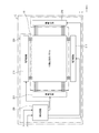
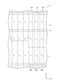
- FIG. 1 It is a block diagram which shows the whole structure of the organic EL display device which concerns on aspect of this disclosure. It is a schematic plan view which enlarged a part of the image display surface of the machine EL panel in the said organic EL display device.
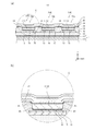
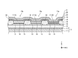
- (A) is a schematic cross-sectional view taken along the line AA of FIG. 2, and (b) is an enlarged view of the broken line circle C of (a).
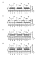
- (A) to (e) are partial cross-sectional views schematically showing a manufacturing process of an organic EL element.
- (A) to (d) are partial cross-sectional views schematically showing the manufacturing process of the organic EL element following FIG.
- FIG. 1 A) and (b) are partial cross-sectional views schematically showing the manufacturing process of the organic EL element following FIG.
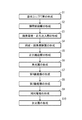
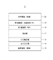
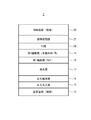
- FIG. 1 A to (d) are partial cross-sectional views schematically showing the manufacturing process of the organic EL element following FIG. It is a flowchart which shows the manufacturing process of an organic EL element. It is a figure which shows typically the laminated structure of the organic EL element which concerns on aspect of this disclosure. It is a table which shows the result of the comparative experiment for verifying the effect of the organic EL element which concerns on the aspect of this disclosure. It is a schematic diagram which shows the laminated structure which concerns on the 1st modification in the 2nd functional layer of an organic EL element. It is a schematic diagram which shows the laminated structure which concerns on the 2nd modification in the 2nd functional layer of an organic EL element.
- FIG. 3 (b) of the organic EL display panel formed thereby. It is an enlarged view of a part.
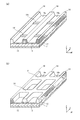
- (A) is a perspective view showing the state of the partition wall in the line bank system, and (b) is a perspective view showing the state of the partition wall in the pixel bank system.
- each functional layer in an organic EL display panel is often formed by a dry process (dry method) such as vacuum deposition, but in recent years, with the progress of coating technology, especially printing equipment technology, wet Technology for forming each functional layer in a process is becoming widespread.
- the wet process is a large display panel in which an ink in which an organic or inorganic functional material is dissolved or dispersed in a solvent is printed on a necessary place by a printing device or the like and then dried to form a functional layer.
- the equipment cost can be suppressed and the material utilization rate is high, which is excellent in terms of cost.
- the light emitting layer is formed by a printing process, it is partitioned by a partition wall so that inks of adjacent sub-pixels are not mixed, and the partition wall is also formed of a resin material by a wet process.
- a cost advantage is achieved.
- an electron transport layer in which an organic material is doped with an alkali metal having a low work function is formed between the cathode and the light emitting layer in order to facilitate the transfer of electrons to the light emitting layer.
- this may be configured to maintain a good carrier balance and optimize the luminous efficiency in the light emitting layer.
- each pixel arranged in a line is partitioned by a bank for each row, and the ink is applied in a band shape (line bank method). May be used.
- the contact area with the functional layer that is the base of the light emitting layer becomes large, and the moisture in the functional layer moves to the electron transport layer, and the characteristics of the electron transport layer may be further deteriorated. Conceivable.
- Such a problem is not limited to an organic EL display panel using an organic EL element as a light emitting element, but a quantum dot display panel in which the light emitting layer is composed of a quantum dot light emitting element (QLED: quantum dot-LED), etc. It can occur commonly for display panels that include elements and that form a functional layer by a wet process. Therefore, the inventors of the present application have diligently researched a configuration in which the luminous efficiency is good and the life is not shortened even when the line bank method is adopted while trying to reduce the cost by adopting the wet process. This is one aspect.
- the self-luminous element according to one aspect of the present disclosure is a self-luminous element in which a light emitting layer is arranged between an anode and a cathode, and is arranged between the light emitting layer and the cathode, and is made of an alkali metal or alkaline soil. It includes a first functional layer containing a fluoride of a metal selected from an earth metal or a rare earth metal, and a second functional layer arranged between the first functional layer and the cathode and containing a rare earth metal as a dope material. ..
- the manufacturing cost can be reduced, the luminous efficiency of the self-luminous element can be improved, and the life of the self-luminous element can be extended.
- the film thickness of the first functional layer is 0.1 nm or more and 20 nm or less.
- the metal fluoride while exhibiting the moisture blocking property of the metal fluoride in the first functional layer, the metal fluoride is partially reduced by the second functional layer containing a rare earth metal as a dope material, so that electron injectability is achieved. It is possible to obtain a self-luminous element having good luminous efficiency and not shortening its life. Further, in the self-luminous element according to another aspect of the present disclosure, in the above aspect, the film thickness of the second functional layer is 5 nm or more and 150 nm or less.
- the second functional layer is arranged on the first layer portion arranged on the first functional layer and the first layer portion.
- the proportion of the rare earth metal contained in the second layer portion is larger than the proportion of the rare earth metal contained in the first layer portion.
- the second functional layer has the first layer portion, the second layer portion and the third layer portion in order from the side closer to the first functional layer.
- the concentration of the rare earth metal in the film thickness direction of the second functional layer is appropriately reduced while exhibiting the water blocking property, and electrons are injected into the light emitting layer.
- the concentration of the rare earth metal in the third layer portion by increasing the concentration of the rare earth metal in the third layer portion, the electron injection property from the cathode side into the second functional layer is improved, and the infiltration of water from the outside is prevented to extend the life of the self-luminous element. It can be extended further.
- the content of the rare earth metal in the second functional layer continuously increases as it approaches the cathode from the first functional layer.
- the water blocking property of the metal fluoride of the first functional layer is exhibited, and the first functional layer is allowed to exert a weak reducing property.
- the electron injectability it is possible to further suppress the invasion of water into the second functional layer, and it is also possible to prevent the light transmission from being lowered more than necessary due to the increase in the doping amount of the rare earth metal.
- the electron injection property from the cathode side into the second functional layer is improved, and the infiltration of water from the outside is prevented, so that the life of the self-luminous element can be further extended. be able to.
- a transparent conductive film is formed as a third functional layer between the second functional layer and the cathode.
- the film thickness of the third functional layer is 15 nm or more. According to this aspect, by adjusting the film thickness of the third functional layer, it is possible to construct an optical resonator structure according to the wavelength of the emission color.
- the self-luminous element according to another aspect of the present disclosure is a thin film having a film thickness of 0.1 nm or more and 3 nm or less containing a rare earth metal between the second functional layer and the third functional layer in the above embodiment. Is formed. Further, in the self-luminous element according to another aspect of the present disclosure, in the above aspect, a thin film having a film thickness of 0.1 nm or more and 3 nm or less containing a rare earth metal is formed between the third functional layer and the cathode. There is.
- a thin film having a film thickness of 0.1 nm or more and 5 nm or less containing a rare earth metal is formed on the opposite side of the cathode from the light emitting layer.
- the anode has light reflectivity and the cathode has semitransparency.
- the light emitted by the light emitting layer is reflected between the first luminous flux directly emitted from the cathode and between the anode and the cathode.
- the film thickness of at least one functional layer including the second luminous flux emitted from the cathode and intervening from the light emitting layer to the cathode so that the first luminous flux and the second luminous flux resonate with each other. , It is set according to the wavelength of the emission color to emit the light.
- an optical resonator composed of an interface between the anode and the interface of the cathode can be constructed, and the luminous efficiency of the self-luminous element can be further improved.
- at least one functional layer interposed between the anode and the cathode is a coating film.
- the fluoride of a metal selected from the alkali metal, alkaline earth metal or rare earth metal is NaF.
- the rare earth metal is Yb.
- a plurality of self-luminous elements according to the above aspect are arranged in a matrix, and at least the light emitting layers in the self-luminous elements adjacent to each other in the row direction extend in the column direction. It is separated by existing partition walls.
- the self-luminous display panel according to another aspect of the present disclosure is a top emission type.
- the aperture ratio of each self-luminous element can be increased and the luminous efficiency is excellent.
- the self-luminous display device includes a self-luminous display panel according to the above aspect and a driving unit that drives the self-luminous display panel to display an image.
- the electronic device includes the self-luminous display device as an image display unit in the above aspect. Such a self-luminous display device and an electronic device are excellent in luminous efficiency of the display panel and can extend the life.
- the method for manufacturing a self-luminous element includes a first step of forming an anode, a second step of forming a light emitting layer above the anode, and an alkali metal on the light emitting layer. , A third step of forming a first functional layer containing a fluoride of a metal selected from an alkaline earth metal or a rare earth metal, and a second functional layer using a rare earth metal as a dope material on the first functional layer. The fourth step of forming and the fifth step of forming a cathode above the second functional layer are included.
- the layer of the organic material is doped with a rare earth metal. It forms a second functional layer.
- the fourth step an organic material and the rare earth metal are co-deposited on the first functional layer to form a second functional layer. Further, the step of forming a hole migration facilitating layer having a hole injecting property and / or a hole transporting function is further included between the first step and the second step, and the hole migration facilitating layer is further included. At least one of the second step, the third step, and the fourth step is executed by the wet process. This facilitates the reduction of manufacturing costs.
- upper does not mean an upward direction (vertically upward) in absolute spatial recognition, but a relative positional relationship based on the stacking order in the laminated structure of the self-luminous element. Is specified by. Specifically, in the self-luminous element, the direction perpendicular to the main surface of the substrate and the direction from the substrate toward the laminate side is the upward direction. Further, for example, the expression “on the substrate” does not mean only the region directly in contact with the substrate, but also includes the region above the substrate via the laminate. Further, for example, when the expression “above the substrate” is used, it does not mean only the upper region separated from the substrate, but also includes the region on the substrate.
- FIG. 1 is a block diagram showing an overall configuration of the organic EL display device 1.
- the organic EL display device 1 is a display device used for, for example, a television, a personal computer, a mobile terminal, a commercial display (electronic signboard, a large screen for commercial facilities), and the like.
- the organic EL display device 1 includes an organic EL display panel 10 and a drive control unit 200 electrically connected to the organic EL display panel 10.
- the organic EL display panel 10 is a top emission type display panel having a rectangular image display surface on the upper surface.
- a plurality of organic EL elements (not shown) are arranged along the image display surface, and the light emission of each organic EL element is combined to display an image.
- the organic EL display panel 10 adopts an active matrix method as an example.
- the drive control unit 200 has a drive circuit 210 connected to the organic EL display panel 10 and a control circuit 220 connected to an external device such as a computer or a receiving device such as an antenna.
- the drive circuit 210 is a power supply circuit that supplies electric power to each organic EL element, a signal circuit that applies a voltage signal that controls the electric power supplied to each organic EL element, and a scan that switches a location where a voltage signal is applied at regular intervals. It has a circuit and so on.
- the control circuit 220 controls the operation of the drive circuit 210 according to data including image information input from an external device or a receiving device.
- four drive circuits 210 are arranged around the organic EL display panel 10 as an example, but the configuration of the drive control unit 200 is not limited to this, and the number of drive circuits 210 is not limited to this. And the position can be changed as appropriate. Further, for the sake of explanation below, as shown in FIG. 1, the direction along the long side of the upper surface of the organic EL display panel 10 is defined as the X direction, and the direction along the short side of the upper surface of the organic EL display panel 10 is defined as the Y direction. ..
- FIG. 2 is a schematic plan view in which a part of the image display surface of the organic EL display panel 10 is enlarged.
- the organic EL display panel 10 as an example, sub-pixels 100R, 100G, and 100B that emit light to R (red), G (green), and B (blue) (hereinafter, also simply referred to as R, G, and B) are arranged in a matrix. They are arranged in a shape.
- the sub-pixels 100R, 100G, and 100B are arranged alternately in the X direction, and a set of sub-pixels 100R, 100G, and 100B arranged in the X direction constitute one pixel P.
- the pixel P it is possible to express full color by combining the emission luminance of the sub-pixels 100R, 100G, and 100B whose gradation is controlled.
- the sub-pixel row CR, the sub-pixel row CG, and the sub-pixel row CB are configured by arranging only one of the sub-pixel 100R, the sub-pixel 100G, and the sub-pixel 100B, respectively.
- the pixels P of the organic EL display panel 10 as a whole are arranged in a matrix along the X and Y directions, and the image is displayed on the image display surface by combining the coloring of the pixels P arranged in the matrix. ..
- Organic EL elements 2 (R), 2 (G), and 2 (B) (see FIG. 3) that emit light in the colors R, G, and B are arranged in the sub-pixels 100R, 100G, and 100B, respectively.
- the organic EL display panel 10 employs a so-called line bank method. That is, a plurality of partition walls (banks) 14 for partitioning the sub-pixel rows CR, CG, and CB for each row are arranged at intervals in the X direction, and in each sub-pixel row CR, CG, and CB, the sub-pixels 100R, 100G, 100B shares a light emitting layer.
- a plurality of pixel regulation layers 141 that insulate the sub-pixels 100R, 100G, and 100B are arranged at intervals in the Y direction, and the sub-pixels 100R, 100G, and 100B are arranged. It can emit light independently.
- the height of the pixel regulation layer 141 is lower than the height of the liquid level when the light emitting layer is coated with ink.
- the partition wall 14 and the pixel regulation layer 141 are represented by dotted lines, which is because the pixel regulation layer 141 and the partition wall 14 are not exposed on the surface of the image display surface and are inside the image display surface. Because it is arranged.
- FIG. 3 (a) is a schematic cross-sectional view taken along the line AA of FIG.
- one pixel is composed of three sub-pixels that emit light of R, G, and B, and each sub-pixel emits the corresponding color of the organic EL elements 2 (R) and 2 (G). ), 2 (B).
- the organic EL elements 2 (R), 2 (G), and 2 (B) of each emission color basically have substantially the same configuration, they will be described as the organic EL element 2 when they are not distinguished.
- the organic EL element 2 includes a substrate 11, an interlayer insulating layer 12, a pixel electrode (anode) 13, a partition wall 14, a hole injection layer 15, a hole transport layer 16, and a light emitting layer 17. It is composed of a first functional layer 18, a second functional layer 19, a counter electrode (cathode) 20, and a sealing layer 21.
- the substrate 11, the interlayer insulating layer 12, the first functional layer 18, the second functional layer 19, the counter electrode 20, and the sealing layer 21 are not formed for each pixel, but are provided in the organic EL display panel 10. It is commonly formed in a plurality of organic EL elements 2.
- the substrate 11 includes a base material 111 which is an insulating material and a TFT (Thin Film Transistor) layer 112. A drive circuit is formed in the TFT layer 112 for each sub-pixel.
- the base material 111 includes, for example, a glass substrate, a quartz substrate, a silicon substrate, molybdenum sulfide, copper, zinc, aluminum, stainless steel, magnesium, iron, nickel, gold, silver and other metal substrates, gallium arsenic and other semiconductor substrates, and plastic substrates. Etc. can be adopted.
- thermoplastic resin either a thermoplastic resin or a thermosetting resin may be used.
- a laminated body in which one type or two or more types are laminated can be used.
- the interlayer insulation layer 12 is formed on the substrate 11.
- the interlayer insulating layer 12 is made of a resin material and is for flattening a step on the upper surface of the TFT layer 112.
- the resin material include a positive type photosensitive material.
- a photosensitive material an acrylic resin, a polyimide resin, a siloxane resin, and a phenol resin can be mentioned.
- contact holes are formed in the interlayer insulating layer 12 for each sub-pixel.
- the pixel electrode 13 includes a metal layer made of a light-reflecting metal material and is formed on the interlayer insulating layer 12.
- the pixel electrode 13 is provided for each sub-pixel and is electrically connected to the TFT layer 112 through a contact hole (not shown). In this embodiment, the pixel electrode 13 functions as an anode.
- the metal material having light reflectivity include Ag (silver), Al (aluminum), aluminum alloy, Mo (molybdenum), APC (alloy of silver, palladium and copper), ARA (silver, rubidium, gold). , MoCr (alloy of molybdenum and chromium), MoW (alloy of molybdenum and tungsten), NiCr (alloy of nickel and chromium) and the like.
- the pixel electrode 13 may be composed of a metal layer alone, but as a laminated structure in which a layer made of a metal oxide such as ITO (indium tin oxide) or IZO (indium tin oxide) is laminated on the metal layer. May be good.
- the partition 14 partitions a plurality of pixel electrodes 13 arranged for each sub-pixel above the substrate 11 for each row in the X direction (see FIG. 2), and is in the X direction. It is a line bank shape extending in the Y direction between the sub-pixel rows CR, CG, and CB arranged in the same direction.
- An electrically insulating material is used for the partition wall 14.
- an electrically insulating material for example, an insulating organic material (for example, acrylic resin, polyimide resin, novolak resin, phenol resin, etc.) is used.
- the partition wall 14 functions as a structure for preventing the applied inks of each color from overflowing and mixing when the light emitting layer 17 is formed by the coating method.
- the partition wall 14 preferably has resistance to an organic solvent and heat. Further, in order to suppress the outflow of ink, it is preferable that the surface of the partition wall 14 has a predetermined liquid repellency. In the portion where the pixel electrode 13 is not formed, the bottom surface of the partition wall 14 is in contact with the upper surface of the interlayer insulating layer 12.
- the pixel regulation layer 141 is made of an electrically insulating material, covers the ends of the pixel electrodes 13 adjacent to the Y direction (FIG. 2) in each sub-pixel row, and partitions the pixel electrodes 13 adjacent to the Y direction. ..
- the height of the pixel regulation layer 141 is slightly larger than the film thickness of the pixel electrode 13, but is lower than the position of the liquid surface when the ink of the light emitting layer is dropped on the opening 14a. Further, the height is higher than the height of the light emitting layer 17 after drying, and the insulating property between the light emitting layers 17 is ensured. As a result, the flow of ink when forming the light emitting layer 17 is not hindered by the pixel regulation layer 141. Therefore, it is easy to make the thickness of the light emitting layer 17 in each sub-pixel row uniform.
- the pixel regulation layer 141 improves the electrical insulation of the pixel electrodes 13 adjacent to each other in the Y direction, suppresses the step breakage of the light emitting layer 17 in each of the sub-pixel rows CR, CG, and CB, and faces the pixel electrodes 13. It has a role of improving the electrical insulation between the electrode 20 and the like.
- Specific examples of the electrically insulating material used for the pixel regulation layer 141 include a resin material and an inorganic material exemplified as the material of the partition wall 14. Further, when the light emitting layer 17 to be the upper layer is formed, it is preferable that the surface of the pixel regulation layer 141 has a liquid property to the ink so that the ink can be easily wetted and spread.
- the hole injection layer 15 is provided on the pixel electrode 13 for the purpose of promoting the injection of holes from the pixel electrode 13 into the light emitting layer 17.
- the hole injection layer 15 is formed by, for example, an oxide such as Ag (silver), Mo (molybdenum), Cr (chromium), V (vanadium), W (tungsten), Ni (nickel), Ir (iridium), or A layer made of a conductive polymeric material such as PEDOT (a mixture of polythiophene and polystyrene sulfonic acid). For example, it may be formed by a sputtering process or a wet process.
- the hole injection layer 15 made of a metal oxide has a large work function and stably injects holes into the light emitting layer 17.
- the hole transport layer 16 has a function of transporting holes injected from the hole injection layer 15 to the light emitting layer 17.
- the hole transport layer 16 is formed by a wet process using, for example, polyfluorene or a derivative thereof, or a polymer compound such as polyarylamine or a derivative thereof, which does not have a hydrophilic group.
- Light-emitting layer 17 is formed in the opening 14a and has a function of emitting light of each color of R, G, and B by recombination of holes and electrons. In particular, when it is necessary to specify and explain the emission color, the emission layers 17 (R), 17 (G), and 17 (B) are described.
- an oxinoid compound for example, an oxinoid compound, a perylene compound, a coumarin compound, an azacumine compound, an oxazole compound, an oxadiazole compound, a perinone compound, a pyrolopyrrole compound, a naphthalene compound, an anthracene compound, a fluorene compound, Fluorantene compounds, tetracene compounds, pyrene compounds, coronene compounds, quinolones and azaquinolones, pyrazoline derivatives and pyrazolone derivatives, rhodamine compounds, chrysene compounds, phenanthrene compounds, cyclopentadiene compounds, styrubene compounds, diphenylquinone compounds, styryl compounds, butadiene compounds, Dicyanomethylenepyran compound, dicyanomethylenethiopyran compound, fluorescein compound, pyririum
- the first functional layer 18 has a function of suppressing the movement of water from the lower organic layer to the second functional layer 19 and transporting electrons from the counter electrode 20 to the light emitting layer 17.
- the first functional layer 18 contains a fluoride of a metal selected from an alkali metal, an alkaline earth metal, or a rare earth metal (hereinafter, referred to as “fluoride such as alkali metal”).
- fluoride such as alkali metal have a dense crystal structure, low moisture permeability and excellent moisture blocking properties, and some alkali metals and the like are liberated by depositing a reducing material on the upper layer. It has the advantage of being excellent in electron injection.
- NaF sodium fluoride
- the first functional layer 18 is also configured to contain NaF in this embodiment.
- ytterbium fluoride (YbF 3 ), lithium fluoride (LiF), and barium fluoride (BaF 2 ) are suitable.
- alkali metal fluoride cerium fluoride (CeF 3 ), lithium fluoride (LiF), sodium fluoride (NaF), as alkaline earth metal fluoride, calcium fluoride (CaF 2 ), magnesium fluoride (MgF 2 ), barium fluoride (BaF 2 ), as rare earth metal fluoride, lanthanum fluoride (LaF 3 ), neodium fluoride (NdF 3 ), samarium fluoride (SmF 3 ), yttrium fluoride (YbF 3 ) , Yttrium fluoride (YF 3 ), gadolinium fluoride (GdF 3 ) and the like may be used.
- the second functional layer 19 has a function of injecting and transporting electrons supplied from the counter electrode 20 toward the light emitting layer 17.
- the second functional layer 19 is formed by using an organic material, particularly an organic material having electron transport property, as a host material and a rare earth metal as a dope material.
- Rare earth metals generally have a low work function, excellent electron injection properties, and reducing properties, and thus have an action of dissociating fluorides such as alkali metals in the first functional layer 18.
- it since it has high chemical stability as compared with alkaline earth metals such as Ba, it is difficult to react with moisture (high water resistance), and a long life can be expected.
- Yb ytterbium
- Yb is used as a dope material.
- the rare earth metal other than Yb La (lantern), Nd (neodymium), Sm (samarium), Eu (europium), Gd (gadolinium), Ce (cerium), Lu (lutetium) and the like may be used. ..
- organic material (host material) having electron transportability for example, a ⁇ -electron low molecular weight organic material such as an oxadiazole derivative (OXD), a triazole derivative (TAZ), and a phenanthroline derivative (BCP, Bphen) can be used. These include, but are not limited to.
- OXD oxadiazole derivative
- TEZ triazole derivative
- BCP, Bphen phenanthroline derivative
- the counter electrode 20 is made of a translucent conductive material and is formed on the second functional layer 19.
- the counter electrode 20 functions as a cathode.
- a metal thin film or a transparent conductive film such as ITO or IZO can be used.
- a metal thin film made of at least one of aluminum, magnesium, silver, aluminum-lithium alloy, magnesium-silver alloy and the like is formed as the material of the counter electrode 20. Is desirable. In this case, the film thickness of the metal thin film is preferably 5 nm or more and 30 nm or less.
- a transparent conductive film such as ITO or IZO is formed between the second functional layer 19 and the counter electrode 20 with a desired film thickness to face the light emitting layer 17. It is desirable to adjust the optical distance between the electrodes 20 to an appropriate size (for details, see the modified example (2) described later).
- the sealing layer 21 prevents organic layers such as the hole transport layer 16, the light emitting layer 17, and the second functional layer 19 from being exposed to moisture or air and deteriorating. It is provided to do so.
- the sealing layer 21 is formed by using a translucent material such as silicon nitride (SiN) or silicon oxynitride (SiON).
- FIG. 3A is an enlarged view of a portion surrounded by a broken line circle C in FIG. 3A. Since the hole transport layer 16 and the light emitting layer 17 are formed by the wet process as described above, the pinnings (contact positions with the partition wall 14) P1 and P2 are higher than those of the central flat portion, respectively. Therefore, by observing the surface shape of each layer, it can be easily determined whether or not the layer is a coating film formed by the wet process.
- FIGS. 4 (a) to (e), FIGS. 5 (a) to 5 (d), FIGS. 6 (a) and 6 (b) and FIGS. 7 (a) to 7 (d) are shown in the manufacture of the organic EL display panel 10. It is a schematic cross-sectional view which shows the state in a process. Further, FIG. 8 is a flowchart showing a manufacturing process of the organic EL display panel 10.
- a TFT layer 112 is formed on the substrate 111 to prepare the substrate 11 (step S1 in FIG. 8).
- the TFT layer 112 can be formed by a known method for manufacturing a TFT.
- the interlayer insulation layer 12 is formed on the substrate 11 (step S2 in FIG. 8).
- a resin material having a certain fluidity is applied, for example, by a die coating method so as to fill the unevenness on the substrate 11 by the TFT layer 112 along the upper surface of the substrate 11.
- the upper surface of the interlayer insulating layer 12 has a flattened shape along the upper surface of the base material 111.
- a contact hole (not shown) is formed in the interlayer insulating layer 12 by performing a dry etching method on a portion of the TFT element, for example, on the source electrode.
- the contact hole is formed by patterning or the like so that the surface of the source electrode is exposed at the bottom thereof.
- connection electrode layer is formed along the inner wall of the contact hole.
- a part of the upper part of the connection electrode layer is arranged on the interlayer insulating layer 12.
- a sputtering method can be used, and after forming a metal film, patterning may be performed using a photolithography method and a wet etching method.
- the pixel electrode material layer 130 is formed on the interlayer insulating layer 12.
- the pixel electrode material layer 130 can be formed by, for example, a vacuum vapor deposition method, a sputtering method, or the like.
- the hole injection material layer 150 is formed on the pixel electrode material layer 130 (FIG. 4 (d)).
- the hole injection material layer 150 can be formed by, for example, a reactive sputtering method or the like. Then, as shown in FIG. 4E, the pixel electrode material layer 130 and the hole injection material layer 150 are patterned by etching, and a plurality of pixel electrodes 13 and hole injection layers 15 partitioned for each sub-pixel are formed. And are formed (step S3 in FIG. 8).
- the method of forming the pixel electrode 13 and the hole injection layer 15 is not limited to the above method.
- the pixel electrode material layer 130 is patterned to form the pixel electrode 13, and then the hole injection layer 15 is formed. You may.
- the partition 14 and the pixel regulation layer 141 are formed (step S4 in FIG. 8).
- the pixel regulation layer 141 and the partition wall 14 are formed in separate steps.
- a photosensitive resin material used as a material for the pixel regulation layer 141 is uniformly applied onto the interlayer insulating layer 12 on which the pixel electrode 13 and the hole injection layer 15 are formed.
- the pixel regulation layer material layer 1410 having a thickness equal to the height of the pixel regulation layer 141 to be formed is formed.
- a specific coating method for example, a wet process such as a die coating method, a slit coating method, or a spin coating method can be used. After application, for example, vacuum drying and 60 ° C. It is preferable that unnecessary solvent is removed by low-temperature heat drying (pre-baking) at about 120 ° C., and the pixel-regulating layer material layer 1410 is fixed to the interlayer insulating layer 12.
- the pixel regulation layer material layer 1410 is patterned by using a photolithography method. For example, when the pixel regulation layer material layer 1410 has positive photosensitivity, the portion to be left as the pixel regulation layer 141 is shielded from light, and the portion to be removed is transparent through a photomask (not shown). 1410 is exposed.
- the pixel regulation layer 141 can be formed by developing and removing the exposed region of the pixel regulation layer material layer 1410.
- a developing solution such as an organic solvent or an alkaline solution that dissolves a portion exposed by exposure of the pixel regulation layer material layer 1410, and then a rinsing solution such as pure water is used.
- the substrate 11 may be washed with.
- firing (post-baking) at a predetermined temperature a pixel regulation layer 141 extending in the X direction can be formed on the interlayer insulating layer 12 (FIG. 5 (b)).
- a partition wall 14 extending in the Y direction is formed in the same manner as the pixel regulation layer 141. That is, the partition wall 14 to be formed by applying a resin material for a partition wall on the interlayer insulating layer 12 on which the pixel electrode 13, the hole injection layer 15, and the pixel regulation layer 141 are formed by using a die coating method or the like.
- a partition wall material layer 140 having a thickness equal to the height of the partition wall material 140 is formed (FIG. 5 (c)), and the partition wall 14 extending in the Y direction is patterned on the partition wall material layer 140 by a photolithography method, and then fired at a predetermined temperature.
- the partition wall 14 is formed (FIG. 5 (d)).
- the material layers of the pixel regulation layer 141 and the partition wall 14 are formed by a wet process and then patterned, but one or both of the material layers are formed by a dry process and a photolithography method is performed. The patterning may be performed by the etching method.
- an ink containing the constituent material of the hole transport layer 16 is applied to the opening 14a defined by the partition wall 14 in a printing apparatus. It is discharged from the nozzle 3011 of the head 301 and applied onto the hole injection layer 15 in the opening 14a. At this time, the ink of the hole transport layer 16 is applied so as to extend along the Y direction (FIG. 2) above the pixel electrode row. Then, it is dried to form the hole transport layer 16 (step S5 in FIG. 8).
- the light-emitting layer 17 is formed above the hole transport layer 16 (step S6 in FIG. 8). Specifically, as shown in FIG. 6B, ink containing a luminescent material having a luminescent color corresponding to each opening 14a is sequentially ejected from the nozzle 3011 of the coating head 301 of the printing apparatus into the opening 14a. Is applied on the hole transport layer 16. At this time, the ink is applied so as to be continuous even above the pixel regulation layer 141. As a result, the ink can flow along the Y direction, the uneven coating of the ink can be reduced, and the film thickness of the light emitting layer 17 in the same sub-pixel row can be made uniform.
- the substrate 11 after the ink is applied is carried into a vacuum drying chamber and heated in a vacuum environment to evaporate the organic solvent in the ink.
- the light emitting layer 17 can be formed.
- the first functional layer 18 is formed on the light emitting layer 17 and the partition wall 14 (step S7 in FIG. 8).
- the first functional layer 18 is formed by forming NaF in common with each sub-pixel by a vapor deposition method.
- a second functional layer 19 is formed on the first functional layer 18 (step S8 in FIG. 8).
- the second functional layer 19 is formed, for example, by forming an electron-transporting organic material and Yb, which is a dope metal, in common with each sub-pixel by a co-evaporation method. Further, Yb may be doped by a sputtering method or the like after first forming a film of an electron-transporting organic material.
- Counter electrode forming step As shown in FIG. 7 (c), the counter electrode 20 is formed on the second functional layer 19 (step S9 in FIG. 8). In the present embodiment, the counter electrode 20 is formed by forming a film of silver, aluminum, or the like by a sputtering method or a vacuum vapor deposition method.
- the sealing layer 21 is formed on the counter electrode 20 (step S10 in FIG. 8).
- the sealing layer 21 can be formed by forming a film of SiON, SiN, or the like by a sputtering method, a CVD method, or the like. As a result, the organic EL display panel 10 is completed.
- FIG. 9 is a diagram schematically showing a laminated structure of a main part (from a pixel electrode (anode) 13 to a counter electrode (cathode) 20) in the organic EL element 2.
- an Al alloy is vapor-deposited on a glass substrate to form a pixel electrode (anode) 13, a hole injection layer 15, a hole transport layer 16, a light emitting layer 17, and a first.
- the functional layer 18, the second functional layer 19, and the counter electrode (cathode) 20 are laminated in this order.
- the first functional layer 18 was a NaF thin film having a film thickness of 2 nm, and was formed by a vacuum deposition method.
- the second functional layer 19 was formed by co-depositing an organic material and Yb so as to have a film thickness of 15 nm.
- the doping concentration of the doping metal Yb is 20 wt%.
- the doping metal of the second functional layer 19 was Ba as the first functional layer 18 in FIG. 9 was not formed.
- This Ba is an alkaline earth metal, has a sufficiently low work function, and has been widely used as an n-type dopant.
- the doping metal of the second functional layer 19 was Yb without forming the first functional layer 18 in FIG.
- the organic EL device according to Comparative Product 3 formed a first functional layer 18 made of NaF, and the doping metal of the second functional layer 19 was Ba.
- the film thickness of the second functional layer of Comparative Products 1 to 3 and the doping concentration of the doping metal were set to 15 nm and 20 wt%, which are the same as those of the present product, respectively. Further, the film thickness of the first functional layer 18 in the comparative product 3 is 2 nm, which is the same as that of the implemented product.
- FIG. 10 is a comparison table showing the results of the luminous efficiency, drive voltage, life, and comprehensive evaluation of the present product and the comparative products 1 to 3.
- the luminous efficiency column shows the luminous efficiency at the initial stage of luminous flux (total luminous flux lm / W per unit power (lumen per watt)) as a comparative value when the luminous efficiency of the product is 100. There is.
- the reciprocal of the drive voltage when a constant current is applied is shown as a comparative value when the implemented product is 100. Since the comparison is made by reciprocal, the higher the value in this column, the lower the drive voltage.
- the life column shows the result of the acceleration experiment. Here, for example, it is determined that the life has been reached when the luminous efficiency becomes 80% or less of the initial value. In this case as well, it is shown as a comparison value when the life of the actual product is 100.
- the doping metal of the second functional layer is Ba, but since it has the first functional layer made of NaF, the electron transport property is complemented, and the evaluation values in terms of luminous efficiency and drive voltage are obtained. Is higher, but slightly less than the examples. However, regarding the lifespan, there is still a difference of 30 points from the actual product. And, only this product was evaluated as " ⁇ " as a comprehensive evaluation.
- the doping metal is Yb in terms of emission efficiency and drive voltage.
- the evaluation is slightly higher in the case where the doping metal is Ba. This is because Yb, which is a rare earth, has lower activity than Ba, which is an alkaline earth metal, reacts with moisture in the process of manufacturing a light emitting device, is less likely to deteriorate, has a low voltage, and suppresses a decrease in the amount of electron current. It is considered that the decrease in efficiency is suppressed by this.
- Yb which is a rare earth metal, has lower activity than Ba, which is an alkaline earth metal, and is less likely to be altered by reacting with moisture. Therefore, Yb is considerably superior to the doping metal from the viewpoint of life.
- C When there is no first functional layer (comparative product 1, comparative product 2), the difference in life is 18% regardless of whether the doping metal of the second functional layer is Ba or Yb.
- the first functional layer of NaF is provided (Comparative Product 3, Implemented Product)
- the difference in life is up to 30% depending on whether the doping metal of the second functional layer is Ba or Yb. It is presumed that this is because the combination of NaF and Yb is compatible, and the synergistic effect thereof forms a long-life organic EL device having better resistance to moisture.
- the film thickness of the first functional layer NaF forming the first functional layer 18 is transferred to the light emitting layer 17 as described above. It has electron injecting property and moisture blocking property, and its film thickness is preferably 0.1 nm or more and 20 nm or less. If the film thickness is less than 0.1 nm, it is too thin to sufficiently exert the effects of electron injection from the second functional layer 19 to the light emitting layer 17 and moisture blocking property to the second functional layer 19. If the film thickness exceeds 20 nm, the reducing action of the second functional layer does not sufficiently act on the first functional layer, and the electron injection property is deteriorated.
- Film thickness of the second functional layer Yb which is a doping metal of the second functional layer 19, has excellent electron injection property from the counter electrode 20 which is a cathode, and has higher transparency than conventional Ba or the like.
- the film thickness can be in the range of 5 nm or more and 150 nm or less. If the film thickness is less than 5 nm, it is too thin to sufficiently reduce NaF, which is the first functional layer, and sufficient electrons cannot be injected from the cathode. If the film thickness exceeds 150 nm, optical adjustment is performed. This is because it is difficult to take out light, the efficiency of light extraction is deteriorated, and the efficiency of light emission may be hindered.
- the thickness of the second functional layer 19 is individually set for each of the emission colors of R, G, and B within this film thickness range by the optical design. It is also possible to set to to construct an optical resonance structure. Since the first functional layer 18 simultaneously has two functions of blocking the movement of water from the lower organic layer to the second functional layer 19 and injecting electrons into the light emitting layer 17, the first function is achieved. It is effective that the layer 18 is directly laminated on the light emitting layer 17 and the second functional layer 19 is directly formed on the first functional layer 18. As a result, it is not necessary to intervene an extra intermediate layer, so that the process load can be reduced.
- Doping concentration of Yb in the second functional layer Yb has a low work function and excellent electron injection property, and its reactivity with water is considerably lower than that of alkali metals and the like. Therefore, the doping concentration of Yb is 1 wt% or more. , 90 wt% or less. If it is less than 1 wt%, the required electron injection property cannot be obtained, and if it exceeds 90 wt%, lumps of Yb are likely to be generated at the time of vapor deposition or the like, and it becomes difficult to evenly disperse it in the organic layer which is the host material. Is.
- the first functional layer 18 made of NaF is formed on the light emitting layer 17, and the second functional layer 19 doped with Yb is formed on the first functional layer 18. is doing.
- the NaF of the first functional layer 18 has a high water blocking ability and can increase the electron injectability by the reducing action of Yb. Therefore, while fulfilling the function of the electron transport layer, the light emitting layer 17 and the partition wall 14 under the first functional layer 18 have a high ability to block water. It is possible to suppress the infiltration of water from the organic layer of the pixel regulation layer 141 into the second functional layer 19.
- Fluoride of a metal selected from an alkali metal other than NaF, an alkaline earth metal, or a rare earth metal can also be used because it has similar characteristics.
- Yb which is a doping metal of the second functional layer 19, is a rare earth element and has a low work function, so that the electron injection property is good, the luminous efficiency is improved, and the drive voltage can be suppressed to a low level.
- the first functional layer 18 suppresses the infiltration of water from the organic layer in the lower layer, and Yb itself has lower reactivity with water than alkali metals and the like, so that it is difficult to deteriorate. If it is a rare earth metal, the same effect can be obtained even if a metal other than Yb is doped. This is because rare earth metals have a low work function and have a reducing property, and mainly have chemical stability as a common property.
- At least one organic layer of the organic EL element 2 is formed by a wet process to reduce the manufacturing cost, and the deterioration of the electron injection property of the second functional layer 19 due to the water content of the organic layer is suppressed to be organic.
- the life of the EL element can be extended.
- FIG. 11 is a schematic view showing a laminated structure of the organic EL element 2 according to the first modification. In the figure, only the laminated structure of the main part (from the pixel electrode 13 to the counter electrode 20) of the organic EL element 2 according to this modification is shown (FIGS. 19, FIG. 20, FIG. 24, and FIG. 25). Except, the same applies to the laminated structure diagram in other modified examples.)
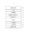
- the side of the second functional layer 19 in which the Yb doping concentration is in contact with the counter electrode 20 is X2 wt%, and the doping concentration decreases as the first functional layer 18 approaches the first functional layer.
- the portion in contact with 18 is configured so that X1 wt% (1 ⁇ X1 ⁇ X2 ⁇ 90).
- the temperature of the electric furnace for heating Yb and the temperature of the electric furnace for heating the organic material are controlled, respectively, to reduce the vapor deposition rate of Yb. This can be achieved by making the deposition rate of the organic material relatively slow.
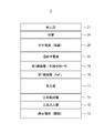
- FIG. 12 is a schematic view showing a laminated structure of the organic EL element 2 according to the second modification.
- the second functional layer 19 has a two-layer structure of the first layer portion 191 and the second layer portion 192, and the Yb dope concentration (X2 wt%) of the second layer portion 192 is the first layer portion. It is higher than the Yb dope concentration (X1 wt%) of 191 (1 ⁇ X1 ⁇ X2 ⁇ 90).
- the second layer portion 192 which is the region on the counter electrode 20 side of the second functional layer 19, has a higher Yb doping concentration than the first layer portion 191 which is the region on the first functional layer 18 side.
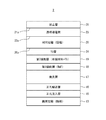
- FIG. 13 is a schematic view showing a laminated structure of the organic EL element 2 according to the second modification.
- the second functional layer 19 has a three-layer structure of the first layer portion 191 and the second layer portion 192, and the third layer portion 193, and the Yb of the first to third layer portions 191 to 193.
- the dope concentrations are X1 wt%, X2 wt%, and X3 wt%, respectively, they are formed so as to satisfy the relationships of X2 ⁇ X1 ⁇ X3 and 1 ⁇ X1 ⁇ X3 ⁇ 90, 0 ⁇ X2.
- the doping concentration of the second layer portion 192 between the first and third layer portions 191 and 193 is set to be the lowest, the amount of Yb doping of the entire second functional layer 19 is increased. It is possible to prevent the light transmission from being lowered more than necessary due to the increase. Since the doping concentration of the first layer portion 191 is high, it is possible to reduce the NaF of the first functional layer 18 while exhibiting the water blocking property, and improve the electron injection property into the light emitting layer. Further, by increasing the concentration of Yb in the third layer portion 193, the electron injection property from the cathode side into the second functional layer is improved, and the infiltration of water from the outside is prevented to extend the life of the organic EL element. The effect that it can be further extended can be obtained.
- FIG. 14 is a schematic view showing a laminated structure according to another aspect of the organic EL element 2. As shown in the figure, a transparent conductive film 23 having a predetermined film thickness is formed between the second functional layer 19 and the counter electrode 20. The transparent conductive film 23 forms ITO, IZO, or the like by a magnetron sputtering method or the like.
- the pair of the counter electrode 20 and the transparent conductive film 23 functions as a cathode, the combined sheet resistance is lowered, and it contributes to the prevention of the decrease in brightness due to the voltage drop. Since ITO and IZO have high transparency, a relatively large film thickness can be obtained, so that they can be used for adjusting the optical path length in the optical resonator structure.
- the film thickness of the transparent conductive film 23 is preferably 15 nm or more. 40 nm or more is more desirable. By setting the film thickness of the transparent conductive film to 15 nm or more, cavity adjustment (film thickness adjustment for the optical resonator structure) can be effectively used, and high efficiency can be realized.
- FIG. 15 is a diagram illustrating light interference in the optical resonator structure of the organic EL element 2 according to this modification.
- the optical resonator structure is formed between the interface of the pixel electrode 13 with the hole injection layer 15 and the interface of the counter electrode 20 with the transparent conductive film 23.
- FIG. 15 shows the main optical paths of the light emitted from the light emitting layer 17.
- the optical path C1 is an optical path in which light emitted from the light emitting layer 17 toward the counter electrode 20 passes through the counter electrode 20 without being reflected.
- the optical path C2 is an optical path in which light emitted from the light emitting layer 17 toward the pixel electrode 13 is reflected by the pixel electrode 13 and passes through the counter electrode 20 via the light emitting layer 17.
- the counter electrode 20 has a semitransparent property that partially reflects the light coming from below.
- such a counter electrode 20 can be achieved by forming a film thickness of 5 nm or more and 30 nm or less by a vapor deposition method using Ag or Al, an alloy thereof or the like as a material.
- the optical path C3 is an optical path in which light emitted from the light emitting layer 17 toward the counter electrode 20 is reflected by the counter electrode 20, further reflected by the pixel electrode 13, and transmitted through the counter electrode 20 via the light emitting layer 17.
- the difference in optical distance (optical path difference) ⁇ C1 between the optical path C1 and the optical path C2 corresponds to twice the length of the optical film thickness L1 shown in FIG.
- the optical film thickness L1 is the total optical distance between the hole injection layer 15 and the hole transport layer 16 from the light emitting layer 17 to the interface with the hole injection layer 15 of the pixel electrode 13 (the thickness and refractive index of each layer). The total value of the products of).
- the optical distance difference ⁇ C2 between the optical path C2 and the optical path C3 corresponds to twice the optical film thickness L2 shown in FIG.
- the optical film thickness L2 is the optical distance between the first functional layer 18, the second functional layer 19, and the transparent conductive film 23 from the light emitting layer 17 to the interface of the counter electrode 20 with the transparent conductive film 23 (thickness and refraction in each layer). The total value of the product with the rate).
- it is necessary to adjust so that the light passing through each of the optical paths C1, the optical path C2, and the optical path C3 is emitted from the organic EL element 2 in the same phase. Therefore, assuming that the target wavelength of the light emitted in FIG. 15 is ⁇ , it is reflected once in the optical path C2 and is deviated by half a wavelength. It is desirable that the optical path difference ⁇ C1 an integral multiple of ⁇ + ⁇ / 2.
- the optical path difference ⁇ C1 is determined by the thickness of the hole injection layer 15 or the hole transport layer 16 and their refractive indexes.
- the optical path difference ⁇ C2 is determined by the thickness and refractive index of the transparent conductive film 23 in FIG. It is desirable to be adjusted by. As described above, since the transparent conductive film 23 has high transparency, even if there is a slight difference in the film thickness of the thin film, the influence is small. Since the wavelength of each emission color is different, the hole injection layer 15, the hole transport layer 16, and the light emission in the organic EL element 2 corresponding to each emission color are changed in order to change the optical path differences ⁇ C1 and ⁇ C2 according to the wavelength. The film thickness of the layer 17 and the film thickness of the transparent conductive film 23 are determined.
- the film thickness may be set so that the optical path difference ⁇ C2 satisfies the above-mentioned resonance condition instead of the transparent conductive film 23 or in combination with the transparent conductive film 23. Further, even when ITO or IZO is formed as a third functional layer on the second functional layer 19 by a sputtering method, the second functional layer 19 can alleviate the sputtering damage, so that the light emitting layer is protected.
- FIG. 16 shows an example of the organic EL display panel 10 reflecting this optical resonator structure.
- the hole injection layer 15 of the organic EL element 2 is positive in the order of red (R), green (G), and blue (B) according to the wavelength of the emission color so as to satisfy the above-mentioned optical resonance condition.
- the total thickness of the hole transport layer 16 and the light emitting layer 17 is reduced.
- FIG. 17 is a schematic view showing a laminated structure according to still another aspect of the organic EL element 2. The difference from the configuration of FIG. 14 is that an intermediate layer (Yb layer) 24 made of Yb is formed between the second functional layer 19 and the transparent conductive film 23.
- Yb layer intermediate layer
- the electron injection property from the counter electrode 20 is further improved, and the overall sheet resistance is reduced when the Yb layer 24, the transparent conductive film 23, and the counter electrode 20 are regarded as a set of cathodes. Even if the panel 10 is enlarged, the voltage drop in the center of the screen can be suppressed and better image quality can be obtained. Further, since Yb has a certain degree of water resistance, it prevents the infiltration of water from the upper layer (transparent conductive film 23, counter electrode 20, sealing layer 21), and causes the lower second functional layer 19 and the like. Deterioration of the light emitting layer 17 can be suppressed and the life can be extended.
- the film thickness of the Yb layer 24 is preferably in the range of 0.1 nm or more and 3 nm or less. If it is less than 0.1 nm, the effects of reducing water resistance and sheet resistance cannot be expected so much, and if it exceeds 3 nm, it may affect the light transmission and rather reduce the luminous efficiency of the organic EL element 2. Because there is.
- FIG. 17 is a schematic view showing a laminated structure according to still another aspect of the organic EL element 2.
- the Yb layer 24 is formed between the transparent conductive film 23 and the counter electrode 20. Even with this configuration, the sheet resistance composed of the pair of the counter electrode 20 and the Yb layer 24 is reduced, so that the voltage drop is reduced, and even if the organic EL display panel 10 is enlarged, the voltage drop at the center of the screen is suppressed. , Better image quality can be obtained.
- the water resistance of Yb prevents the infiltration of moisture from the upper layer (counter electrode 20, sealing layer 21), and suppresses deterioration of the transparent conductive film 23, the second functional layer 19, and the light emitting layer 17 of the lower layer. , The life can be extended. According to this configuration, the transparent conductive film 23 can also be protected from external moisture.
- the film thickness of the Yb layer 24 in this modification is also preferably in the range of 0.1 nm or more and 3 nm or less for the same reason as in (3-1) above.
- FIG. 19 is a schematic view showing a laminated structure according to still another aspect of the organic EL element 2.
- the Yb layer 24 is formed on the outside of the counter electrode 20 (on the side opposite to the light emitting layer 17) and between the sealing layer 21 and the sealing layer 21.
- the voltage drop due to the sheet resistance of the counter electrode 20 can be reduced, and even if the organic EL display panel 10 becomes large, the voltage drop at the center of the screen can be suppressed and better image quality can be obtained.
- the Yb layer 24 is provided outside the counter electrode 20, it does not have the effect of reinforcing the electron injection property.
- the water resistance of Yb prevents the infiltration of moisture from the upper layer (sealing layer 21), suppresses deterioration of the transparent conductive film 23, the second functional layer 19, and the light emitting layer 17 of the lower layer, and prolongs the service life. Can be planned.
- the film thickness of the Yb layer 24 in this modification is preferably in the range of 0.1 nm or more and 5 nm or less. If it is less than 0.1 nm, the effects of reducing water resistance and sheet resistance cannot be expected so much, and if it exceeds 5 nm, it may affect the light transmission and rather reduce the luminous efficiency of the organic EL element 2. Because there is.
- FIG. 20 is a schematic view showing a laminated structure according to still another aspect of the organic EL element 2.
- the transparent conductive film 23 is formed on the outside of the counter electrode 20 (on the side opposite to the light emitting layer 17) and between the sealing layer 21 and the sealing layer 21.
- the counter electrode 20 is formed of Ag (refractive index 0.05)
- the transparent conductive film 23 is formed of IZO (refractive index 2.05)
- the sealing layer 21 is SiN (refractive index).
- the interface 23a between the counter electrode 20 and the transparent conductive film 23 and the interface 21a between the transparent conductive film 23 and the sealing layer 21 can serve as reflective surfaces.
- each cavity has a spectrum having a different peak wavelength.
- Light is generated, and light having a spectrum having a peak wavelength formed by synthesizing those spectra is output from the organic EL element 2. Therefore, by appropriately setting the refractive index and the film thickness of the counter electrode 20 and the transparent conductive film 23, it is possible to obtain the effect that the chromaticity of the output light can be finely adjusted.
- the transparent conductive film 23 is made of an IZO film which is a transparent conductive film and is formed in direct contact with the counter electrode 20, the voltage drop due to the sheet resistance of the counter electrode 20 is reduced, and the organic EL display panel 10 is large. Even if the image quality is changed, the voltage drop in the center of the screen can be suppressed and better image quality can be obtained.
- the transparent conductive film 23 may be another transparent conductive film, for example, an ITO film.
- a single layer or a multi-layer rare earth metal layer containing another rare earth metal may be used.
- the partition wall 14 and the pixel regulation layer 141 are formed in different steps, but the partition wall 14 and the pixels are formed by using a halftone mask.
- the regulation layer 141 may be formed at the same time.
- a resin material is applied on the interlayer insulating layer 12 on which the pixel electrode 13 and the hole injection layer 15 are formed by a wet process such as a die coating method to form a partition wall material layer 140 (see FIG. 5C). do.
- the coating it is preferable that, for example, vacuum drying and low-temperature heat drying (pre-baking) at about 60 ° C. to 120 ° C. are performed to remove unnecessary solvents and the partition wall material layer is fixed to the interlayer insulating layer 12.
- pre-baking vacuum drying and low-temperature heat drying
- the partition material layer 140 is exposed through a photomask (not shown). For example, when the partition wall material layer 140 has positive photosensitivity, the portion where the partition wall material layer 140 is left is shielded from light, and the portion to be removed is exposed.
- the pixel regulation layer 141 Since the pixel regulation layer 141 has a smaller film thickness than the partition wall 14, it is necessary to semi-expose the partition wall material layer 140 on the portion of the pixel regulation layer 141. Therefore, as a photomask used in the exposure process, a light-shielding portion arranged at a position corresponding to the partition wall 14 to completely block light, a translucent portion arranged at a position corresponding to the pixel regulation layer 141, and other parts. A halftone mask having a translucent portion arranged at a position corresponding to an exposed portion of the pixel electrode 13 of the above is used.
- the translucency of the translucent portion is determined so that when exposed for a predetermined time, the partition wall material layer 140 on the pixel electrode 13 is fully exposed, and the pixel restricting layer 141 remains unexposed by the height thereof. NS.
- a specific developing method for example, the entire substrate 11 is immersed in a developing solution such as an organic solvent or an alkaline solution that dissolves the exposed portion of the partition wall material layer 140, and then the substrate is rinsed with a rinsing solution such as pure water. 11 may be washed. Then, it is fired at a predetermined temperature.
- the partition wall 14 extending in the Y direction and the pixel restricting layer 141 extending in the X direction can be formed on the interlayer insulating layer 12 in the same process. Since the number can be reduced, it contributes to cost reduction in manufacturing organic EL display panels.
- the first functional layer 18, the second functional layer 19, the hole injection layer 15 and the hole transport layer 16 are provided as the laminated structure of the organic EL element. Although it is said that it has a configuration, it is not limited to this. For example, it may be an organic EL device that does not have the hole transport layer 16. Further, for example, a single hole injection transport layer may be provided instead of the hole injection layer 15 and the hole transport layer 16.
- the stretching direction of the pixel regulation layer 141 is the long axis X direction of the organic EL display panel 10
- the stretching direction of the partition wall 14 is the organic EL.
- the stretching directions of the pixel regulation layer 141 and the partition wall 14 may be opposite to each other. Further, the stretching direction of the pixel regulation layer and the partition wall may be a direction irrelevant to the shape of the organic EL display panel 10.
- the image display surface is rectangular as an example, but the shape of the image display surface is not limited and can be changed as appropriate.
- the pixel electrode 13 is a rectangular flat plate-shaped member, but the present invention is not limited to this.
- the hole injection layer 15 is formed by a dry process, but after the pixel electrode 13 is formed, the pixel regulation layer 141 and the partition wall 14 are formed, and then shown in FIG. 21 (a).
- the hole injection layer 15 may be formed in the openings 14a between the adjacent partition walls 14 by a wet process.
- the film shape of the hole injection layer 15 is also wet because the position P3 in contact with the partition wall 14 is located above the central flat portion. It can be easily known that the coating film is formed of.
- sub-pixels 100R, 100G, and 100B that emit light in R, G, and B colors are arranged, but the emission color of the sub-pixels is not limited to this.
- the emission color of the sub-pixels is not limited to this.
- four colors of yellow (Y) may be used.
- the number of sub-pixels is not limited to one per color, and a plurality of sub-pixels may be arranged.
- the arrangement of the sub-pixels in the pixel P is not limited to the order of red, green, and blue as shown in FIG. 2, and may be in the order in which these are interchanged.
- FIG. 22A shows a schematic partial perspective view at the stage where the pixel regulation layer 141 and the partition wall 14 are formed in the line bank type organic EL display panel 10. Since the pixel regulation layer 141 that defines the range of sub-pixels in the Y direction is lower in height than the partition wall 14, when ink is continuously applied to the opening 14a, the ink flows in the Y direction to increase the film thickness by leveling. It has the advantage of being easy to make uniform, but on the other hand, it also has the disadvantage that the area of contact between the light emitting layer 17 and the first functional layer 18 formed by the wet process becomes large, and moisture easily penetrates into the upper layer.
- FIG. 22B is a partial perspective view schematically showing the shape of the partition wall 14 in the pixel bank system.
- the light emitting layer 17 cannot be further expanded, and the contact area between the first functional layer 18 and the light emitting layer 17 is a line. Since it is limited as compared with the bank method, there is an advantage that the amount of water that may infiltrate into the first functional layer 18 is reduced, and deterioration of the first functional layer 18 and the second functional layer 19 is further suppressed. In this respect, it can be said to be superior to the line bank method.
- FIG. 23 is a schematic cross-sectional view showing a laminated structure of a bottom emission type organic EL display panel. It differs from the top-emission type organic EL display panel 10 described with reference to FIG. 3 in the following points.
- the counter electrode 20 does not have to be transparent, and may have reflectivity. As a result, the film thickness of the counter electrode 20 can be increased, a material having high conductivity can be used, and the sheet resistance can be reduced, so that the variation in brightness due to the voltage drop of the counter electrode 20 can be eliminated. In addition, the thicker film thickness can be expected to have a sealing effect by the counter electrode 20.
- the pixel electrode 13 is formed of a transparent conductive film such as IZO or ITO, and the interlayer insulating layer 12 is formed of a transparent resin material.
- a drive circuit for a light emitting element using a TFT is formed in a first region 1121 that overlaps with a partition wall 14 (or a pixel regulation layer 141) in a plan view, and a second region 1122 between them has translucency. In this way, it is configured so as not to block the emitted light.
- the base material 111 is also formed of a translucent resin sheet or a glass sheet.
- the counter electrode 20 may be a light-reflecting anode
- the pixel electrode 13 may be made of a light-transmitting (including semi-light-transmitting) material to serve as a cathode.
- the stacking order of the other hole injection layer 15, the hole transport layer 16, the first functional layer 18, and the second functional layer 19 is also the reverse of that shown in FIG. Since the material 111 is thick, there is an advantage that the sealing property is very high and the second functional layer 19 is less likely to deteriorate.
- a color filter substrate or a polarizing plate is provided, if they are attached to the substrate 11 or the substrate 11 itself is also used as the color filter substrate or the polarizing plate, the configuration can be simplified and the cost can be reduced. Can be planned.
- this bottom emission type organic EL display panel by making the counter electrode 20 also transparent, it is possible to provide a transmission type organic EL display panel.
- a transmission type organic EL display panel For example, by arranging the transmissive organic EL display panel 10 on the windshield of a car, a car navigation guidance screen, a speedometer of the car, etc. can be displayed without obstructing the front view until driving is hindered. This makes it possible to further expand the fields of use of the organic EL display panel 10.
- the sealing layer 21 is formed as a single layer using a translucent inorganic material such as silicon nitride (SiN) or silicon oxynitride (SiON), but these inorganic materials are sealed. Although it has excellent properties, it has the disadvantage that it is easily cracked by external force and is vulnerable to bending action. If the film thickness of the sealing layer of the inorganic material is increased in order to prevent the occurrence of cracks, the rigidity is increased and the flexibility is greatly impaired. Therefore, recently, a device has been made to reduce the film thickness of the inorganic material layer in the sealing layer and to absorb the impact due to the external force by stacking the resin material layers to ensure flexibility and prevent cracks from occurring. There is.
- FIG. 24 is a schematic view showing an example of a laminated structure of an organic EL display panel (flexible display panel) 400 having excellent flexibility according to this modification.
- the flexible display panel 400 includes a substrate 411, an interlayer insulating layer 412, a light emitting main portion 430, and a sealing layer 421.
- the substrate 411 has a UC (undercoat) layer 4112 formed on the resin film 4111 which is a base material, and a TFT layer 4113 formed on the UC layer 4112.
- the resin film 4111 is made of a resin material having flexibility and excellent heat resistance.
- PET polyethylene terephthalate
- a thin UC layer 4112 made of an inorganic material such as SiN or SiON is laminated on the resin film 4111 below. The infiltration of water from the water is blocked to protect the TFT layer 4113 from deterioration due to water.
- a light emitting main portion 430 is arranged on the substrate 411 via an interlayer insulating layer 412.
- the light emitting main part 430 has a laminated structure similar to that of the light emitting main part in the embodiment (see FIG. 9), and the hole injection layer 415 and the hole transport layer 416 are placed on the pixel electrode 413.
- the light emitting layer 417, the first functional layer 418, the second functional layer 419, and the counter electrode 420 are laminated in this order. Since each of these components has the same contents as those described in the embodiments, detailed description thereof will be omitted.
- a sealing layer 421 is formed on the counter electrode 420 of the light emitting main portion 430.
- the sealing layer 421 has a three-layer structure of a first sealing layer 4211, a second sealing layer 4212, and a third sealing layer 4213.
- the first sealing layer 4211 is formed by a dry process such as a sputtering method or a CVD method using a translucent inorganic material such as SiN or SiON
- the second sealing layer 4212 is formed by, for example, a fluorine-based material or a fluorine-based material.
- a translucent resin material such as an acrylic material or an epoxy material is formed on the first sealing layer 4211 by a wet process such as a coating method.
- a third sealing layer 4213 is formed on the third sealing layer 4213 in the same manner as the first sealing layer 4211.
- the base material of the substrate is formed of a resin film, and the sealing layer is flexible by sandwiching a film (organic material layer) made of a resin material between two thin films (inorganic material layer) made of an inorganic material.
- the display panel having a structure for ensuring the property and the sealing property by adopting Yb as the dope metal of the second functional layer 419 as in the above embodiment, the water resistance is increased, so that the sealing layer 421 is also used, for example. Sufficient durability can be obtained by stacking the inorganic film and the organic film one by one. This makes it possible to simplify the sealing structure of the flexible display panel 400.
- such a flexible display panel makes it easy to install in an automobile with many curves.
- the temperature inside the vehicle may become high, but rare earth metals such as Yb generally have a standard reduction potential as compared with Ba (barium), which has been conventionally used as a dope metal. Since it is high, it is chemically stable even if the temperature rises a little, and it does not easily react with impurities such as moisture, so high temperature durability can be increased accordingly, and it can be used for a long time in a harsh temperature environment. It becomes.
- a known resin film polarizing plate (more specifically, a circular polarizing plate formed by combining a linear polarizing plate and a quarter wave plate) may be further attached onto the sealing layer 421. do not have. As a result, the light incident on the inside of the flexible display panel 400 from the outside can be prevented from being reflected internally and emitted to the outside, and in particular, the visibility of the display image of the flexible display panel 400 outdoors can be improved. can. It also has the advantage of being able to suppress the intrusion of impurities such as moisture from the outside.
- OCCF on-chip color filter
- the light emitting main portion 430 in the flexible display panel 400 according to the present modification is not limited to the configuration shown in FIG. 9, and can be widely applied to all the configurations described in the modification.
- FIG. 25 is a schematic view showing a laminated structure of a main part of a tandem type organic EL element 500, and the substrate and the sealing layer are not shown.
- the organic EL element includes an anode (pixel electrode) 501, a hole injection transport layer 502, a light emitting layer 503, a NaF layer (first functional layer) 504, and a Yb-doped layer (second).
- Functional layer) 505 charge generation layer 506, hole injection transport layer 507, light emitting layer 508, NaF layer (first functional layer) 509, Yb-doped layer (second functional layer) 510, and cathode (opposite electrode) 511. It is laminated in this order.
- the charge generation layer 506 in the middle is formed of, for example, MoO 3 as an inorganic P-type oxide, supplies holes to the hole injection transport layer 507, and supplies holes to the Yb-doped layer 505. It has a function of supplying electrons.
- the light emitting layer 503 emits B color (blue) light
- the light emitting layer 508 emits Y color (yellow) light. Since blue and yellow are almost complementary colors, they are combined and finally light of a color close to white is emitted.
- the combination of emission colors is not limited to this, and other emission colors may be freely combined to output light of a desired color. Even in the case of such a tandem type organic EL element 500, the combination of the Yb-doped layer and the NaF layer improves the electron injection property and durability, and can contribute to the improvement of luminous efficiency and the extension of life.
- the organic EL display panel shown in the above embodiment can be used as a display panel for various electronic devices such as a display unit 601 of a television device 600 and other personal computers, mobile terminals, and commercial displays. Can be used.
- the organic EL display panel 10 according to the above embodiment adopts an active matrix method, but the present invention is not limited to this, and a passive matrix method may be adopted.
- QLED Quantum dot Light Emitting Diode
- the present invention can be applied when the coating method is adopted for forming the light emitting layer and other functional layers.
- the present invention can be applied when the coating method is adopted for forming the light emitting layer and other functional layers.
- the self-luminous element according to the present disclosure can be widely used in a display panel used in various electronic devices.
- Organic EL display device 2 Organic EL display panel 10
- Organic EL display panel 11 Organic EL display panel 11
- Organic EL display panel 12 Organic EL display panel 11
- 411 Substrate 12 412 Thin film transistor 13, 413 Pixel electrode 14
- 415 Hole injection layer 16, 416 Hole transport layer 17, 417
- Sealing layer 4211 1st sealing layer 4212 2nd sealing layer 4213 3rd sealing layer 23 Transparent thin film transistor 24 Yb layer 100B, 100G, 100R Sub-pixel 111, 4111 Base material 112, 4113 TFT layer 4112 UC layer 140 Partition material layer 141 Pixel regulation layer 191 First layer part 192 Second layer part 193 Third layer part
Landscapes
- Engineering & Computer Science (AREA)
- Manufacturing & Machinery (AREA)
- Electroluminescent Light Sources (AREA)
Abstract
画素電極(陽極)13と対向電極(陰極)20との間に発光層17が配された自発光素子であって、前記発光層17と対向電極20との間に配され、アルカリ金属、アルカリ土類金属もしくは希土類金属から選択された金属のフッ化物を含む第1機能層18と、前記第1機能層18と前記対向電極20との間に配され、希土類金属をドープ材料として含む第2機能層19とを備える。
Description
本発明は、例えば、有機電界発光素子(以下「有機EL素子」と称する)などの自発光素子、及びその製造方法、並びに当該自発光素子を基板上に行列状に配した自発光表示パネル、当該自発光表示パネルを画像表示部として用いた自発光表示装置、電子機器に関する。
近年、自発光型のディスプレイとして、基板上に行列方向に沿って有機EL素子を複数配列した有機EL表示パネルが、電子機器のディスプレイとして実用化されている。
各有機EL素子は、陽極と陰極の一対の電極対の間に有機発光材料を含む有機発光層(以下、単に「発光層」という。)が配設された基本構造を有し、駆動時に一対の電極対間に電圧を印加し、陽極から発光層に注入される正孔と、陰極から発光層に注入される電子との再結合に伴って光が発生する電流駆動型の自発光素子である。
各有機EL素子は、陽極と陰極の一対の電極対の間に有機発光材料を含む有機発光層(以下、単に「発光層」という。)が配設された基本構造を有し、駆動時に一対の電極対間に電圧を印加し、陽極から発光層に注入される正孔と、陰極から発光層に注入される電子との再結合に伴って光が発生する電流駆動型の自発光素子である。
通常、このような有機EL表示パネルにあっては、陰極からの発光層への電子の注入性を向上させるために、陰極と発光層との間に電子輸送層が設けられている。この電子輸送層として、例えば、特許文献1には、有機層に、アルカリ金属やアルカリ土類金属(以下、「アルカリ金属等」と称する。)の化合物を含有させた構成が開示されている。
このようなアルカリ金属等は、仕事関数が低く、陰極から電子を注入・輸送する能力が高いので、有機EL素子の発光効率を向上させることができる。
このようなアルカリ金属等は、仕事関数が低く、陰極から電子を注入・輸送する能力が高いので、有機EL素子の発光効率を向上させることができる。
また、上記特許文献1では、高温により電子輸送層におけるアルカリ金属等が、発光層に拡散して、発光特性が劣化しないように電子輸送層と発光層と間に、バッファ層を設けている。このバッファ層は、Alq3、4,4’-N,N’-ジカルバゾール-ビフェニル(CBP)、ジスチリルアリーレン(DSA)、DPB、BAlq、またはアントラセン誘導体化合物Irなどの有機化合物からなる。
ところで、発光層を始めとする機能層、特に有機機能層は、水分を吸収・透過しやすいという物性を有している。一方、電子輸送層に含まれるアルカリ金属等は、活性が高く、機能層に含まれる水分とすぐに反応して変質し、電子注入特性が劣化して有機EL表示パネルが短寿命化するという問題がある。
特に、最近では、製造コスト面での優位性から、特定の機能を有する材料(機能性材料:有機材料のみならず無機材料も含まれる。)を溶媒に溶解または分散させた溶液(以下、単に「インク」と称する。)を、印刷装置等で塗布して機能層を形成するウエットプロセス(湿式法)が多く用いられているが、この場合には、機能層中の水分残留量が、蒸着法などのドライプロセス(乾式法)によって成膜する場合よりも格段に多く、上記特許文献1の構成では、バッファ層が有機化合物からなるため、それより下層の有機層中の水分が当該バッファ層を介して電子輸送層に浸透して、電子輸送層中のアルカリ金属等と反応し、発光特性が劣化するおそれがある。
特に、最近では、製造コスト面での優位性から、特定の機能を有する材料(機能性材料:有機材料のみならず無機材料も含まれる。)を溶媒に溶解または分散させた溶液(以下、単に「インク」と称する。)を、印刷装置等で塗布して機能層を形成するウエットプロセス(湿式法)が多く用いられているが、この場合には、機能層中の水分残留量が、蒸着法などのドライプロセス(乾式法)によって成膜する場合よりも格段に多く、上記特許文献1の構成では、バッファ層が有機化合物からなるため、それより下層の有機層中の水分が当該バッファ層を介して電子輸送層に浸透して、電子輸送層中のアルカリ金属等と反応し、発光特性が劣化するおそれがある。
本開示は、上述のような課題に鑑みてなされたものであって、少なくとも1つの機能層をウエットプロセスで形成することにより製造コストを低減しつつ、良好な発光効率を確保すると共に、長寿命化が可能な自発光素子、及びその製造方法、並びに当該自発光素子を基板上に行列状に配した自発光表示パネル、当該自発光表示パネルを画像表示部として用いた自発光表示装置、電子機器を提供することを目的とする。
本開示の一態様に係る自発光素子は、陽極と陰極との間に発光層が配された自発光素子であって、前記発光層と前記陰極との間に配され、アルカリ金属、アルカリ土類金属もしくは希土類金属から選択された金属のフッ化物を含む第1機能層と、前記第1機能層と前記陰極との間に配され、希土類金属をドープ材料として含む第2機能層とを備えることを特徴とする。
また、本開示の別の態様に係る自発光素子の製造方法は、陽極を形成する第1工程と、前記陽極の上方に発光層を形成する第2工程と、前記発光層上に、アルカリ金属、アルカリ土類金属もしくは希土類金属から選択された金属のフッ化物を含む第1機能層を形成する第3工程と、前記第1機能層上に、希土類金属をドープ材料とする第2機能層を形成する第4工程と、前記第2機能層の上方に、陰極を形成する第5工程と、を含むことを特徴とする。
上記態様に係る自発光素子および自発光素子の製造方法によれば、少なくとも1つの機能層をウエットプロセスで形成することにより製造コストを低減しつつ、良好な発光効率を確保すると共に、長寿命化が可能な自発光素子や自発光表示パネル、自発光表示装置、電子機器を提供できる。
≪本開示の一態様に至った経緯≫
有機EL表示パネルにおける各機能層は、従来は真空蒸着などのドライプロセス(乾式法)により成膜される場合が多かったが、塗布技術、特に印刷装置の技術の進歩に伴い、近年では、ウエットプロセスで各機能層を形成する技術が普及しつつある。
ウエットプロセスは、有機もしくは無機の機能性材料が溶媒に溶解もしくは分散したインクを、印刷装置等により必要箇所に印刷した後、乾燥させて機能層を形成するものであり、大型の表示パネルであってもその設備費が抑制できると共に材料利用率が高いなどコスト面で優れているからである。
有機EL表示パネルにおける各機能層は、従来は真空蒸着などのドライプロセス(乾式法)により成膜される場合が多かったが、塗布技術、特に印刷装置の技術の進歩に伴い、近年では、ウエットプロセスで各機能層を形成する技術が普及しつつある。
ウエットプロセスは、有機もしくは無機の機能性材料が溶媒に溶解もしくは分散したインクを、印刷装置等により必要箇所に印刷した後、乾燥させて機能層を形成するものであり、大型の表示パネルであってもその設備費が抑制できると共に材料利用率が高いなどコスト面で優れているからである。
各種機能層のうち、特に、発光層を印刷プロセスで形成する場合、隣接する副画素同士のインクが混ざらないようにするため、隔壁で仕切られており、当該隔壁もウエットプロセスにより樹脂材料で形成することにより、コスト的な優位性が図られている。
特許文献1にもあるように、陰極と発光層の間には、電子の発光層への移動を容易にするために、有機材料に低仕事関数のアルカリ金属等をドープした電子輸送層を形成し、これにより良好なキャリアバランスを維持して発光層における発光効率が最適になるように構成されている場合がある。
特許文献1にもあるように、陰極と発光層の間には、電子の発光層への移動を容易にするために、有機材料に低仕事関数のアルカリ金属等をドープした電子輸送層を形成し、これにより良好なキャリアバランスを維持して発光層における発光効率が最適になるように構成されている場合がある。
しかし、アルカリ金属等は、活性が高く、上述のように隔壁や発光層の樹脂材料中にわずかでも水分が含まれていると、やがて、その水分が、電子注入層に浸透し、電子輸送層中のアルカリ金属等が当該水分と反応して変質して電子注入性が著しく劣化してしまう。これにより、発光効率が劣化し、短寿命となるおそれがあることが分かった。
特許文献1では、電子輸送層と発光層との間に、Alq3、4,4’-N,N’-ジカルバゾール-ビフェニル(CBP)などからなるバッファ層を設けているが、いずれも有機材料を含んでいるので、電子輸送層への水分の浸入を抑制するという点では十分機能していない。
特許文献1では、電子輸送層と発光層との間に、Alq3、4,4’-N,N’-ジカルバゾール-ビフェニル(CBP)などからなるバッファ層を設けているが、いずれも有機材料を含んでいるので、電子輸送層への水分の浸入を抑制するという点では十分機能していない。
また、最近では、発光層のインクを、迅速かつ均一に塗布するため、ライン状に配列された各画素を、その列毎にバンクで仕切って、インクを帯状に塗布する方法(ラインバンク方式)を用いることがある。この場合には、発光層の下地となる機能層との接触面積が大きくなり、機能層中の水分が電子輸送層に移動して、ますます、電子輸送層の特性が劣化してしまうことが考えられる。
このような問題は、発光素子として有機EL素子を用いた有機EL表示パネルに限らず、発光層が、量子ドット発光素子(QLED:quantum dot-LED)からなる量子ドット表示パネルなど、およそ自発光素子を備え、ウエットプロセスにより機能層を形成する表示パネルについて共通に生じ得る。
そこで、本願発明者らは、ウエットプロセスを採用して低コスト化を図りつつ、ラインバンク方式を採用した場合でも、発光効率が良好で寿命が短くならない構成を求めて鋭意研究した結果、本開示の一態様に至ったものである。
≪本開示の一態様の概要≫
本開示の一態様に係る自発光素子は、陽極と陰極との間に発光層が配された自発光素子であって、前記発光層と前記陰極との間に配され、アルカリ金属、アルカリ土類金属もしくは希土類金属から選択された金属のフッ化物を含む第1機能層と、前記第1機能層と前記陰極との間に配され、希土類金属をドープ材料として含む第2機能層とを備える。
そこで、本願発明者らは、ウエットプロセスを採用して低コスト化を図りつつ、ラインバンク方式を採用した場合でも、発光効率が良好で寿命が短くならない構成を求めて鋭意研究した結果、本開示の一態様に至ったものである。
≪本開示の一態様の概要≫
本開示の一態様に係る自発光素子は、陽極と陰極との間に発光層が配された自発光素子であって、前記発光層と前記陰極との間に配され、アルカリ金属、アルカリ土類金属もしくは希土類金属から選択された金属のフッ化物を含む第1機能層と、前記第1機能層と前記陰極との間に配され、希土類金属をドープ材料として含む第2機能層とを備える。
係る態様により、少なくとも1つの機能層をウエットプロセスで形成することにより製造コストを低減しつつ、自発光素子の発光効率を向上させると共に長寿命化を可能とする。
また、本開示の別の態様に係る自発光素子は、上記態様において、前記第1機能層の膜厚が、0.1nm以上20nm以下である。
また、本開示の別の態様に係る自発光素子は、上記態様において、前記第1機能層の膜厚が、0.1nm以上20nm以下である。
係る態様により、第1機能層における金属フッ化物による水分ブロック性を発揮しつつ、当該金属フッ化物が、希土類金属をドープ材料として含む第2機能層によって部分的に還元されることで電子注入性を確保し、発光効率が良好で寿命が短くならない自発光素子を得ることができる。
また、本開示の別の態様に係る自発光素子は、上記態様において、前記第2機能層の膜厚が、5nm以上150nm以下である。
また、本開示の別の態様に係る自発光素子は、上記態様において、前記第2機能層の膜厚が、5nm以上150nm以下である。
係る態様により、第1機能層における金属フッ化物の水分ブロック性を発揮させつつ、当該金属フッ化物の一部を還元し、かつ、第2機能層に含まれる希土類金属の電子注入性の効果を発揮することができる。また、第2機能層上に第3機能層としてスパッタ法で製膜される例えばITOやIZOが製膜されるときにおいてもそのスパッタダメージを緩和し、発光効率が良好で寿命が短くならない自発光素子を得ることができる。
また、本開示の別の態様に係る自発光素子は、上記態様において、前記第2機能層は、前記第1機能層上に配された第1層部分と、前記第1層部分上に配された第2層部分とを含み、前記第2層部分における前記希土類金属の含有の割合が、前記第1層部分における前記希土類金属の含有の割合よりも大きい。
また、本開示の別の態様に係る自発光素子は、上記態様において、前記第2機能層が、第1機能層に近い側から第1層部分、第2層部分および第3層部分を順に積層してなり、前記第1層部分、第2層部分、第3層部分における前記希土類金属の含有の割合をそれぞれ、X1、X2、X3とすると、X2<X1≦X3である。
また、本開示の別の態様に係る自発光素子は、上記態様において、前記第2機能層が、第1機能層に近い側から第1層部分、第2層部分および第3層部分を順に積層してなり、前記第1層部分、第2層部分、第3層部分における前記希土類金属の含有の割合をそれぞれ、X1、X2、X3とすると、X2<X1≦X3である。
このように第2機能層の膜厚方向において希土類金属の濃度を変化させることにより、第1機能層の金属フッ化物の水分ブロック性を発揮しつつ、適切に還元させ、発光層への電子注入性を向上させることが出来るとともに、希土類金属のドープ量の増加によって光透過性が必要以上に低下しないようにすることもできる。また、第3層部分の希土類金属の濃度を高くすることにより陰極側からの第2機能層への電子注入性を向上するとともに外部からの水分の浸入を阻止して、自発光素子の寿命を更に延ばせることができる。
また、本開示の別の態様に係る自発光素子は、上記態様において、前記第2機能層における希土類金属の含有量は、第1機能層から陰極に近付くに連れて連続的に多くなる。
このように第2機能層の希土類金属の含有量を連続して変化させることで第1機能層の金属フッ化物の水分ブロック性を発揮しつつ、第1機能層には弱い還元性を作用させ、電子注入性は制限しつつも水分の第2機能層への侵入をより抑制でき、希土類金属のドープ量の増加によって光透過性が必要以上に低下しないようにすることもできる。また、陰極側の希土類金属の濃度を高くすることで陰極側からの第2機能層への電子注入性を向上するとともに外部からの水分の浸入を阻止して、自発光素子の寿命を更に延ばせることができる。
このように第2機能層の希土類金属の含有量を連続して変化させることで第1機能層の金属フッ化物の水分ブロック性を発揮しつつ、第1機能層には弱い還元性を作用させ、電子注入性は制限しつつも水分の第2機能層への侵入をより抑制でき、希土類金属のドープ量の増加によって光透過性が必要以上に低下しないようにすることもできる。また、陰極側の希土類金属の濃度を高くすることで陰極側からの第2機能層への電子注入性を向上するとともに外部からの水分の浸入を阻止して、自発光素子の寿命を更に延ばせることができる。
また、本開示の別の態様に係る自発光素子は、上記態様において、第2機能層と陰極との間に、第3機能層として透明導電膜が形成されている。
また、本開示の別の態様に係る自発光素子は、上記態様において、前記第3機能層の膜厚は、15nm以上である。
係る態様によれば、第3機能層の膜厚を調整することにより、発光色の波長に応じた光共振器構造を構築することが可能となる。
また、本開示の別の態様に係る自発光素子は、上記態様において、前記第3機能層の膜厚は、15nm以上である。
係る態様によれば、第3機能層の膜厚を調整することにより、発光色の波長に応じた光共振器構造を構築することが可能となる。
また、本開示の別の態様に係る自発光素子は、上記態様において、前記第2機能層と前記第3機能層との間に、希土類金属を含む膜厚0.1nm以上、3nm以下の薄膜が形成されている。
また、本開示の別の態様に係る自発光素子は、上記態様において、前記第3機能層と陰極との間に、希土類金属を含む膜厚0.1nm以上、3nm以下の薄膜が形成されている。
また、本開示の別の態様に係る自発光素子は、上記態様において、前記第3機能層と陰極との間に、希土類金属を含む膜厚0.1nm以上、3nm以下の薄膜が形成されている。
また、本開示の別の態様に係る自発光素子は、上記態様において、前記陰極の前記発光層とは反対側に、希土類金属を含む膜厚0.1nm以上、5nm以下の薄膜が形成されている。
係る態様により、陰極の膜質を向上することが出来ることに加え、外部からの水分の浸入を阻止して、自発光素子の寿命を更に延ばせることができる。
係る態様により、陰極の膜質を向上することが出来ることに加え、外部からの水分の浸入を阻止して、自発光素子の寿命を更に延ばせることができる。
また、本開示の別の態様に係る自発光素子は、上記態様において、前記陽極は、光反射性を有すると共に、前記陰極は、半透過性を有する。
ここで、本開示の別の態様に係る自発光素子は、上記態様において、前記発光層で発光された光は、前記陰極から直接射出される第1光束と、前記陽極と前記陰極間で反射した後、前記陰極から射出される第2光束とを含み、第1光束と第2光束が共振するように、前記発光層から前記陰極に至るまでに介在する少なくとも一つの機能層の膜厚が、当該発光する発光色の波長に応じて設定されている。
ここで、本開示の別の態様に係る自発光素子は、上記態様において、前記発光層で発光された光は、前記陰極から直接射出される第1光束と、前記陽極と前記陰極間で反射した後、前記陰極から射出される第2光束とを含み、第1光束と第2光束が共振するように、前記発光層から前記陰極に至るまでに介在する少なくとも一つの機能層の膜厚が、当該発光する発光色の波長に応じて設定されている。
係る態様により、陽極の界面と陰極の界面間で構成される光共振器を構築することができ、自発光素子の発光効率のさらに向上を可能にする。
本開示の別の態様に係る自発光素子は、前記陽極と前記陰極との間に介在する少なくとも一つの機能層が塗布膜である。
本開示の別の態様に係る自発光素子は、前記アルカリ金属、アルカリ土類金属もしくは希土類金属から選択された金属のフッ化物は、NaFである。
また、本開示の別の態様に係る自発光素子では、前記希土類金属が、Ybである。
また、本開示の別の態様に係る自発光表示パネルは、上記態様に係る自発光素子を複数、行列状に配列し、少なくとも行方向に隣接する自発光素子における発光層は、列方向に延在する隔壁によって仕切られている。
本開示の別の態様に係る自発光素子は、前記陽極と前記陰極との間に介在する少なくとも一つの機能層が塗布膜である。
本開示の別の態様に係る自発光素子は、前記アルカリ金属、アルカリ土類金属もしくは希土類金属から選択された金属のフッ化物は、NaFである。
また、本開示の別の態様に係る自発光素子では、前記希土類金属が、Ybである。
また、本開示の別の態様に係る自発光表示パネルは、上記態様に係る自発光素子を複数、行列状に配列し、少なくとも行方向に隣接する自発光素子における発光層は、列方向に延在する隔壁によって仕切られている。
これにより、発光効率に優れ、長寿命化が可能な自発光表示パネルを提供することができる。
また、本開示の別の態様に係る自発光表示パネルは、トップエミッション型である。
トップエミッション型の自発光表示パネルでは、光を射出する方向に、TFTなどからなる駆動回路が配されていないので、各自発光素子の開口率を大きくでき、発光効率に優れる。
また、本開示の別の態様に係る自発光表示パネルは、トップエミッション型である。
トップエミッション型の自発光表示パネルでは、光を射出する方向に、TFTなどからなる駆動回路が配されていないので、各自発光素子の開口率を大きくでき、発光効率に優れる。
また、本開示の別の態様に係る自発光表示装置は、上記態様に係る自発光表示パネルと、前記自発光表示パネルを駆動して画像を表示させる駆動部とを備える。
また、本開示の別の態様に係る電子機器は、上記態様において、画像表示部として上記自発光表示装置を備える。
係る自発光表示装置および電子機器は、表示パネルの発光効率に優れ、寿命も長くすることができる。
また、本開示の別の態様に係る電子機器は、上記態様において、画像表示部として上記自発光表示装置を備える。
係る自発光表示装置および電子機器は、表示パネルの発光効率に優れ、寿命も長くすることができる。
また、本開示の別の態様に係る自発光素子の製造方法は、陽極を形成する第1工程と、前記陽極の上方に発光層を形成する第2工程と、前記発光層上に、アルカリ金属、アルカリ土類金属もしくは希土類金属から選択された金属のフッ化物を含む第1機能層を形成する第3工程と、前記第1機能層上に、希土類金属をドープ材料とする第2機能層を形成する第4工程と、前記第2機能層の上方に、陰極を形成する第5工程とを含む。
係る態様により、上述のように発光効率に優れた良質な画像を表示できる自発光素子の製造が可能となる。
また、本開示の別態様に係る自発光素子の製造方法は、前記第4工程が、第1機能層上に有機材料の層を形成した後、当該有機材料の層に希土類金属をドープして第2機能層を形成する。
また、本開示の別態様に係る自発光素子の製造方法は、前記第4工程が、第1機能層上に有機材料の層を形成した後、当該有機材料の層に希土類金属をドープして第2機能層を形成する。
また、本開示の別態様に係る自発光表示素子の製造方法は、前記第4工程は、第1機能層上に有機材料と前記希土類金属を共蒸着して第2機能層を形成する。
また、前記第1工程と第2工程の間に、正孔注入性および/または正孔輸送性の機能を有する正孔移動容易化層を形成する工程をさらに含み、前記正孔移動容易化層の形成工程および前記第2工程、第3工程、第4工程のうち、少なくとも一つの工程は、ウエットプロセスにより実行される。
これにより製造コストの低減化が容易となる。
また、前記第1工程と第2工程の間に、正孔注入性および/または正孔輸送性の機能を有する正孔移動容易化層を形成する工程をさらに含み、前記正孔移動容易化層の形成工程および前記第2工程、第3工程、第4工程のうち、少なくとも一つの工程は、ウエットプロセスにより実行される。
これにより製造コストの低減化が容易となる。
なお、上記各開示の態様において「上」とは、絶対的な空間認識における上方向(鉛直上方)を指すものではなく、自発光素子の積層構造における積層順を基に、相対的な位置関係により規定されるものである。具体的には、自発光素子において、基板の主面に垂直な方向であって、基板から積層物側に向かう側を上方向とする。また、例えば「基板上」と表現した場合は、基板に直接接する領域のみを指すのではなく、積層物を介した基板の上方の領域も含めるものとする。また、例えば「基板の上方」と表現した場合、基板と間隔を空けた上方領域のみを指すのではなく、基板上の領域も含めるものとする。
≪実施の形態≫
以下、本開示の一態様に係る有機EL素子および有機EL表示パネル、有機EL表示装置について、図面を参照しながら説明する。なお、図面は、模式的なものを含んでおり、各部材の縮尺や縦横の比率などが実際とは異なる場合がある。
1.有機EL表示装置1の全体構成
図1は、有機EL表示装置1の全体構成を示すブロック図である。有機EL表示装置1は、例えば、テレビ、パーソナルコンピュータ、携帯端末、業務用ディスプレイ(電子看板、商業施設用大型スクリーン)などに用いられる表示装置である。
以下、本開示の一態様に係る有機EL素子および有機EL表示パネル、有機EL表示装置について、図面を参照しながら説明する。なお、図面は、模式的なものを含んでおり、各部材の縮尺や縦横の比率などが実際とは異なる場合がある。
1.有機EL表示装置1の全体構成
図1は、有機EL表示装置1の全体構成を示すブロック図である。有機EL表示装置1は、例えば、テレビ、パーソナルコンピュータ、携帯端末、業務用ディスプレイ(電子看板、商業施設用大型スクリーン)などに用いられる表示装置である。
有機EL表示装置1は、有機EL表示パネル10と、これに電気的に接続された駆動制御部200とを備える。
有機EL表示パネル10は、本実施の形態では、上面が長方形状の画像表示面であるトップエミッション型の表示パネルである。有機EL表示パネル10では、画像表示面に沿って複数の有機EL素子(不図示)が配列され、各有機EL素子の発光を組み合わせて画像を表示する。なお、有機EL表示パネル10は、一例として、アクティブマトリクス方式を採用している。
有機EL表示パネル10は、本実施の形態では、上面が長方形状の画像表示面であるトップエミッション型の表示パネルである。有機EL表示パネル10では、画像表示面に沿って複数の有機EL素子(不図示)が配列され、各有機EL素子の発光を組み合わせて画像を表示する。なお、有機EL表示パネル10は、一例として、アクティブマトリクス方式を採用している。
駆動制御部200は、有機EL表示パネル10に接続された駆動回路210と、計算機などの外部装置又はアンテナなどの受信装置に接続された制御回路220とを有する。駆動回路210は、各有機EL素子に電力を供給する電源回路、各有機EL素子への供給電力を制御する電圧信号を印加する信号回路、一定の間隔ごとに電圧信号を印加する箇所を切り替える走査回路などを有する。
制御回路220は、外部装置や受信装置から入力された画像情報を含むデータに応じて、駆動回路210の動作を制御する。
なお、図1では、一例として、駆動回路210が有機EL表示パネル10の周囲に4つ配置されているが、駆動制御部200の構成はこれに限定されるものではなく、駆動回路210の数や位置は適宜変更可能である。また、以下では説明のため、図1に示すように、有機EL表示パネル10上面の長辺に沿った方向をX方向、有機EL表示パネル10上面の短辺に沿った方向をY方向とする。
なお、図1では、一例として、駆動回路210が有機EL表示パネル10の周囲に4つ配置されているが、駆動制御部200の構成はこれに限定されるものではなく、駆動回路210の数や位置は適宜変更可能である。また、以下では説明のため、図1に示すように、有機EL表示パネル10上面の長辺に沿った方向をX方向、有機EL表示パネル10上面の短辺に沿った方向をY方向とする。
2.有機EL表示パネル10の構成
(A)平面構成
図2は、有機EL表示パネル10の画像表示面の一部を拡大した模式平面図である。有機EL表示パネル10では、一例として、R(赤色)、G(緑色)、B(青色)(以下、単にR、G、Bともいう。)にそれぞれ発光する副画素100R、100G、100Bが行列状に配列されている。副画素100R、100G、100Bは、X方向に交互に並び、X方向に並ぶ一組の副画素100R、100G、100Bが、一つの画素Pを構成している。画素Pでは、階調制御された副画素100R、100G、100Bの発光輝度を組み合わせることにより、フルカラーを表現することが可能である。
(A)平面構成
図2は、有機EL表示パネル10の画像表示面の一部を拡大した模式平面図である。有機EL表示パネル10では、一例として、R(赤色)、G(緑色)、B(青色)(以下、単にR、G、Bともいう。)にそれぞれ発光する副画素100R、100G、100Bが行列状に配列されている。副画素100R、100G、100Bは、X方向に交互に並び、X方向に並ぶ一組の副画素100R、100G、100Bが、一つの画素Pを構成している。画素Pでは、階調制御された副画素100R、100G、100Bの発光輝度を組み合わせることにより、フルカラーを表現することが可能である。
また、Y方向においては、副画素100R、副画素100G、副画素100Bのいずれかのみが並ぶことでそれぞれ副画素列CR、副画素列CG、副画素列CBが構成されている。これにより、有機EL表示パネル10全体として画素Pが、X方向及びY方向に沿った行列状に並び、この行列状に並ぶ画素Pの発色を組み合わせることにより、画像表示面に画像が表示される。
副画素100R、100G、100Bには、それぞれR、G、Bの色に発光する有機EL素子2(R)、2(G)、2(B)(図3参照)が配置されている。
また、本実施の形態に係る有機EL表示パネル10では、いわゆるラインバンク方式を採用している。すなわち、副画素列CR、CG、CBを1列ごとに仕切る隔壁(バンク)14がX方向に間隔をおいて複数配置され、各副画素列CR、CG、CBでは、副画素100R、100G、100Bが、発光層を共有している。
また、本実施の形態に係る有機EL表示パネル10では、いわゆるラインバンク方式を採用している。すなわち、副画素列CR、CG、CBを1列ごとに仕切る隔壁(バンク)14がX方向に間隔をおいて複数配置され、各副画素列CR、CG、CBでは、副画素100R、100G、100Bが、発光層を共有している。
ただし、各副画素列CR、CG、CBでは、副画素100R、100G、100B同士を絶縁する画素規制層141がY方向に間隔をおいて複数配置され、各副画素100R、100G、100Bは、独立して発光することができるようになっている。
なお、画素規制層141の高さは、発光層のインク塗布時における液面の高さよりも低い。図2では、隔壁14及び画素規制層141は点線で表されているが、これは、画素規制層141及び隔壁14が、画像表示面の表面に露出しておらず、画像表示面の内部に配置されているからである。
なお、画素規制層141の高さは、発光層のインク塗布時における液面の高さよりも低い。図2では、隔壁14及び画素規制層141は点線で表されているが、これは、画素規制層141及び隔壁14が、画像表示面の表面に露出しておらず、画像表示面の内部に配置されているからである。
(B)断面構成
図3(a)は、図2のA-A線に沿った模式断面図である。
有機EL表示パネル10において、一つの画素は、R、G、Bをそれぞれ発光する3つの副画素からなり、各副画素は、対応する色を発光する有機EL素子2(R)、2(G)、2(B)で構成される。
図3(a)は、図2のA-A線に沿った模式断面図である。
有機EL表示パネル10において、一つの画素は、R、G、Bをそれぞれ発光する3つの副画素からなり、各副画素は、対応する色を発光する有機EL素子2(R)、2(G)、2(B)で構成される。
各発光色の有機EL素子2(R)、2(G)、2(B)は、基本的には、ほぼ同様の構成を有するので、区別しないときは、有機EL素子2として説明する。
図3(a)に示すように、有機EL素子2は、基板11、層間絶縁層12、画素電極(陽極)13、隔壁14、正孔注入層15、正孔輸送層16、発光層17、第1機能層18、第2機能層19、対向電極(陰極)20、および、封止層21とからなる。
図3(a)に示すように、有機EL素子2は、基板11、層間絶縁層12、画素電極(陽極)13、隔壁14、正孔注入層15、正孔輸送層16、発光層17、第1機能層18、第2機能層19、対向電極(陰極)20、および、封止層21とからなる。
基板11、層間絶縁層12、第1機能層18、第2機能層19、対向電極20、および、封止層21は、画素ごとに形成されているのではなく、有機EL表示パネル10が備える複数の有機EL素子2に共通して形成されている。
(1)基板
基板11は、絶縁材料である基材111と、TFT(Thin Film Transistor)層112とを含む。TFT層112には、副画素ごとに駆動回路が形成されている。基材111は、例えば、ガラス基板、石英基板、シリコン基板、硫化モリブデン、銅、亜鉛、アルミニウム、ステンレス、マグネシウム、鉄、ニッケル、金、銀などの金属基板、ガリウム砒素などの半導体基板、プラスチック基板等を採用することができる。
(1)基板
基板11は、絶縁材料である基材111と、TFT(Thin Film Transistor)層112とを含む。TFT層112には、副画素ごとに駆動回路が形成されている。基材111は、例えば、ガラス基板、石英基板、シリコン基板、硫化モリブデン、銅、亜鉛、アルミニウム、ステンレス、マグネシウム、鉄、ニッケル、金、銀などの金属基板、ガリウム砒素などの半導体基板、プラスチック基板等を採用することができる。
プラスチック材料としては、熱可塑性樹脂、熱硬化樹脂いずれの樹脂を用いてもよい。例えば、ポリエチレン、ポリプロピレン、ポリアミド、ポリイミド(PI)、ポリカーボネート、アクリル系樹脂、ポリエチレンテレフタレート(PET)、ポリブチレンテレフタレート、ポリアセタール、その他フッ素系樹脂、スチレン系、ポリオレフィン系、ポリ塩化ビニル系、ポリウレタン系、フッ素ゴム系、塩素化ポリエチレン系等の各種熱可塑性エラストマー、エポキシ樹脂、不飽和ポリエステル、シリコーン樹脂、ポリウレタン等、またはこれらを主とする共重合体、ブレンド体、ポリマーアロイ等が挙げられ、これらのうち1種、または2種以上を積層した積層体を用いることができる。
(2)層間絶縁層
層間絶縁層12は、基板11上に形成されている。層間絶縁層12は、樹脂材料からなり、TFT層112の上面の段差を平坦化するためのものである。樹脂材料としては、例えば、ポジ型の感光性材料が挙げられる。また、このような感光性材料として、アクリル系樹脂、ポリイミド系樹脂、シロキサン系樹脂、フェノール系樹脂が挙げられる。また、図3の断面図には示されていないが、層間絶縁層12には、副画素ごとにコンタクトホールが形成されている。
層間絶縁層12は、基板11上に形成されている。層間絶縁層12は、樹脂材料からなり、TFT層112の上面の段差を平坦化するためのものである。樹脂材料としては、例えば、ポジ型の感光性材料が挙げられる。また、このような感光性材料として、アクリル系樹脂、ポリイミド系樹脂、シロキサン系樹脂、フェノール系樹脂が挙げられる。また、図3の断面図には示されていないが、層間絶縁層12には、副画素ごとにコンタクトホールが形成されている。
(3)画素電極
画素電極13は、光反射性の金属材料からなる金属層を含み、層間絶縁層12上に形成されている。画素電極13は、副画素ごとに設けられ、コンタクトホール(不図示)を通じてTFT層112と電気的に接続されている。
本実施の形態においては、画素電極13は、陽極として機能する。
画素電極13は、光反射性の金属材料からなる金属層を含み、層間絶縁層12上に形成されている。画素電極13は、副画素ごとに設けられ、コンタクトホール(不図示)を通じてTFT層112と電気的に接続されている。
本実施の形態においては、画素電極13は、陽極として機能する。
光反射性を具備する金属材料の具体例としては、Ag(銀)、Al(アルミニウム)、アルミニウム合金、Mo(モリブデン)、APC(銀、パラジウム、銅の合金)、ARA(銀、ルビジウム、金の合金)、MoCr(モリブデンとクロムの合金)、MoW(モリブデンとタングステンの合金)、NiCr(ニッケルとクロムの合金)などが挙げられる。
画素電極13は、金属層単独で構成してもよいが、金属層の上に、ITO(酸化インジウム錫)やIZO(酸化インジウム亜鉛)のような金属酸化物からなる層を積層した積層構造としてもよい。
(4)隔壁・画素規制層
隔壁14は、基板11の上方に副画素ごとに配置された複数の画素電極13を、X方向(図2参照)において列毎に仕切るものであって、X方向に並ぶ副画素列CR、CG、CBの間においてY方向に延伸するラインバンク形状である。
(4)隔壁・画素規制層
隔壁14は、基板11の上方に副画素ごとに配置された複数の画素電極13を、X方向(図2参照)において列毎に仕切るものであって、X方向に並ぶ副画素列CR、CG、CBの間においてY方向に延伸するラインバンク形状である。
この隔壁14には、電気絶縁性材料が用いられる。電気絶縁性材料の具体例として、例えば、絶縁性の有機材料(例えば、アクリル系樹脂、ポリイミド系樹脂、ノボラック樹脂、フェノール樹脂等)が用いられる。
隔壁14は、発光層17を塗布法で形成する場合に塗布された各色のインクが溢れて混色しないようにするための構造物として機能する。
隔壁14は、発光層17を塗布法で形成する場合に塗布された各色のインクが溢れて混色しないようにするための構造物として機能する。
なお、樹脂材料を用いる際は、加工性の点から感光性を有することが好ましい。当該感光性は、ポジ型、ネガ型のいずれであってもよい。
隔壁14は、有機溶媒や熱に対する耐性を有することが好ましい。また、インクの流出を抑制するために、隔壁14の表面は所定の撥液性を有することが好ましい。
画素電極13が形成されていない部分において、隔壁14の底面が層間絶縁層12の上面と接している。
隔壁14は、有機溶媒や熱に対する耐性を有することが好ましい。また、インクの流出を抑制するために、隔壁14の表面は所定の撥液性を有することが好ましい。
画素電極13が形成されていない部分において、隔壁14の底面が層間絶縁層12の上面と接している。
画素規制層141は、電気絶縁性材料からなり、各副画素列においてY方向(図2)に隣接する画素電極13の端部を覆い、当該Y方向に隣接する画素電極13同士を仕切っている。
画素規制層141の高さは、画素電極13の膜厚よりも若干大きいが、発光層のインクが開口部14aに滴下されたときの液面の位置よりも低くなっている。また、乾燥後の発光層17の高さよりも高く、発光層17同士の絶縁性を確保する。
これにより、発光層17を形成する際のインクの流動が画素規制層141に妨げられない。そのため、各副画素列における発光層17の厚みを均一に揃えることを容易にする。
画素規制層141の高さは、画素電極13の膜厚よりも若干大きいが、発光層のインクが開口部14aに滴下されたときの液面の位置よりも低くなっている。また、乾燥後の発光層17の高さよりも高く、発光層17同士の絶縁性を確保する。
これにより、発光層17を形成する際のインクの流動が画素規制層141に妨げられない。そのため、各副画素列における発光層17の厚みを均一に揃えることを容易にする。
画素規制層141は、上記構造により、Y方向に隣接する画素電極13の電気絶縁性を向上しつつ、各副画素列CR、CG、CBにおける発光層17の段切れ抑制、画素電極13と対向電極20との間の電気絶縁性の向上などの役割を有する。
画素規制層141に用いられる電気絶縁性材料の具体例としては、上記隔壁14の材料として例示した樹脂材料や無機材料などが挙げられる。また、上層となる発光層17を形成する際、インクが濡れ広がりやすいように、画素規制層141の表面はインクに対する親液性を有することが好ましい。
画素規制層141に用いられる電気絶縁性材料の具体例としては、上記隔壁14の材料として例示した樹脂材料や無機材料などが挙げられる。また、上層となる発光層17を形成する際、インクが濡れ広がりやすいように、画素規制層141の表面はインクに対する親液性を有することが好ましい。
(5)正孔注入層
正孔注入層15は、画素電極13から発光層17への正孔の注入を促進させる目的で、画素電極13上に設けられている。正孔注入層15は、例えば、Ag(銀)、Mo(モリブデン)、Cr(クロム)、V(バナジウム)、W(タングステン)、Ni(ニッケル)、Ir(イリジウム)などの酸化物、あるいは、PEDOT(ポリチオフェンとポリスチレンスルホン酸との混合物)などの導電性ポリマー材料からなる層である。例えばスパッタプロセスやウエットプロセスにより形成しても良い。
正孔注入層15は、画素電極13から発光層17への正孔の注入を促進させる目的で、画素電極13上に設けられている。正孔注入層15は、例えば、Ag(銀)、Mo(モリブデン)、Cr(クロム)、V(バナジウム)、W(タングステン)、Ni(ニッケル)、Ir(イリジウム)などの酸化物、あるいは、PEDOT(ポリチオフェンとポリスチレンスルホン酸との混合物)などの導電性ポリマー材料からなる層である。例えばスパッタプロセスやウエットプロセスにより形成しても良い。
上記のうち、酸化金属からなる正孔注入層15は、仕事関数が大きく、発光層17に対し安定的に正孔を注入する。
(6)正孔輸送層
正孔輸送層16は、正孔注入層15から注入された正孔を発光層17へ輸送する機能を有する。正孔輸送層16は、例えば、ポリフルオレンやその誘導体、あるいは、ポリアリールアミンやその誘導体などの高分子化合物であって、親水基を備えないものなどを用いてウエットプロセスにより形成される。
(6)正孔輸送層
正孔輸送層16は、正孔注入層15から注入された正孔を発光層17へ輸送する機能を有する。正孔輸送層16は、例えば、ポリフルオレンやその誘導体、あるいは、ポリアリールアミンやその誘導体などの高分子化合物であって、親水基を備えないものなどを用いてウエットプロセスにより形成される。
(7)発光層
発光層17は、開口部14a内に形成されており、正孔と電子の再結合により、R、G、Bの各色の光を発光する機能を有する。なお、特に、発光色を特定して説明する必要があるときには、発光層17(R)、17(G)、17(B)と記す。
発光層17の材料として、具体的には、例えば、オキシノイド化合物、ペリレン化合物、クマリン化合物、アザクマリン化合物、オキサゾール化合物、オキサジアゾール化合物、ペリノン化合物、ピロロピロール化合物、ナフタレン化合物、アントラセン化合物、フルオレン化合物、フルオランテン化合物、テトラセン化合物、ピレン化合物、コロネン化合物、キノロン化合物及びアザキノロン化合物、ピラゾリン誘導体及びピラゾロン誘導体、ローダミン化合物、クリセン化合物、フェナントレン化合物、シクロペンタジエン化合物、スチルベン化合物、ジフェニルキノン化合物、スチリル化合物、ブタジエン化合物、ジシアノメチレンピラン化合物、ジシアノメチレンチオピラン化合物、フルオレセイン化合物、ピリリウム化合物、チアピリリウム化合物、セレナピリリウム化合物、テルロピリリウム化合物、芳香族アルダジエン化合物、オリゴフェニレン化合物、チオキサンテン化合物、シアニン化合物、アクリジン化合物、8-ヒドロキシキノリン化合物の金属錯体、2-ビピリジン化合物の金属錯体、シッフ塩とIII族金属との錯体、オキシン金属錯体、希土類錯体などの蛍光物質で形成されることが好ましい。
発光層17は、ウエットプロセスにより形成される。
発光層17は、開口部14a内に形成されており、正孔と電子の再結合により、R、G、Bの各色の光を発光する機能を有する。なお、特に、発光色を特定して説明する必要があるときには、発光層17(R)、17(G)、17(B)と記す。
発光層17の材料として、具体的には、例えば、オキシノイド化合物、ペリレン化合物、クマリン化合物、アザクマリン化合物、オキサゾール化合物、オキサジアゾール化合物、ペリノン化合物、ピロロピロール化合物、ナフタレン化合物、アントラセン化合物、フルオレン化合物、フルオランテン化合物、テトラセン化合物、ピレン化合物、コロネン化合物、キノロン化合物及びアザキノロン化合物、ピラゾリン誘導体及びピラゾロン誘導体、ローダミン化合物、クリセン化合物、フェナントレン化合物、シクロペンタジエン化合物、スチルベン化合物、ジフェニルキノン化合物、スチリル化合物、ブタジエン化合物、ジシアノメチレンピラン化合物、ジシアノメチレンチオピラン化合物、フルオレセイン化合物、ピリリウム化合物、チアピリリウム化合物、セレナピリリウム化合物、テルロピリリウム化合物、芳香族アルダジエン化合物、オリゴフェニレン化合物、チオキサンテン化合物、シアニン化合物、アクリジン化合物、8-ヒドロキシキノリン化合物の金属錯体、2-ビピリジン化合物の金属錯体、シッフ塩とIII族金属との錯体、オキシン金属錯体、希土類錯体などの蛍光物質で形成されることが好ましい。
発光層17は、ウエットプロセスにより形成される。
(8)第1機能層
第1機能層18は、下部の有機層からの水分の第2機能層19への移動を抑止すると共に、対向電極20からの電子を発光層17へ輸送する機能を有する。第1機能層18は、アルカリ金属、アルカリ土類金属もしくは希土類金属から選択された金属のフッ化物(以下、「アルカリ金属等フッ化物」という。)を含む。
一般に、アルカリ金属等フッ化物は、結晶構造が緻密で、水分の透過性が低く水分ブロック性に優れると共に、上層に還元性を有する材料を蒸着することで一部のアルカリ金属等が遊離して電子注入性に優れるというメリットがある。その中でも特に、NaF(フッ化ナトリウム)が、水分ブロック性と電子注入性に優れており、本実施の形態でも第1機能層18は、NaFを含む構成としている。
第1機能層18は、下部の有機層からの水分の第2機能層19への移動を抑止すると共に、対向電極20からの電子を発光層17へ輸送する機能を有する。第1機能層18は、アルカリ金属、アルカリ土類金属もしくは希土類金属から選択された金属のフッ化物(以下、「アルカリ金属等フッ化物」という。)を含む。
一般に、アルカリ金属等フッ化物は、結晶構造が緻密で、水分の透過性が低く水分ブロック性に優れると共に、上層に還元性を有する材料を蒸着することで一部のアルカリ金属等が遊離して電子注入性に優れるというメリットがある。その中でも特に、NaF(フッ化ナトリウム)が、水分ブロック性と電子注入性に優れており、本実施の形態でも第1機能層18は、NaFを含む構成としている。
なお、上記フッ化ナトリウム以外の金属フッ化物として、例えば、フッ化イッテルビウム(YbF3)、フッ化リチウム(LiF)、フッ化バリウム(BaF2)が好適である。その他に、アルカリ金属フッ化物として、フッ化セリウム(CeF3)、フッ化リチウム(LiF)、フッ化ナトリウム(NaF)、アルカリ土類金属フッ化物として、フッ化カルシウム(CaF2)、フッ化マグネシウム(MgF2)、フッ化バリウム(BaF2)、希土類金属フッ化物として、フッ化ランタン(LaF3)、フッ化ネオジウム(NdF3)、フッ化サマリウム(SmF3)、フッ化イッテルビウム(YbF3)、フッ化イットリウム(YF3)、フッ化ガドリニウム(GdF3)等を用いてもよい。
上記第1機能層18による、発光層17や正孔輸送層16に含まれる水分の第2機能層19への浸入をブロックする効果や、第2機能層19から発光層17への電子注入性向上の効果を十分発揮するためには、第1機能層18が、発光層17上に直接積層されていることが望ましい。
上記第1機能層18による、発光層17や正孔輸送層16に含まれる水分の第2機能層19への浸入をブロックする効果や、第2機能層19から発光層17への電子注入性向上の効果を十分発揮するためには、第1機能層18が、発光層17上に直接積層されていることが望ましい。
(9)第2機能層19
第2機能層19は、対向電極20から供給される電子を発光層17側へと注入・輸送する機能を有する。第2機能層19は、有機材料、特に、電子輸送性を有する有機材料をホスト材料とし、希土類金属をドープ材料として形成されている。希土類金属は、総じて仕事関数が低く電子注入性に優れると共に、還元性を有しているので、第1機能層18におけるアルカリ金属等フッ化物を解離させる作用を備える。また、Baなどのアルカリ土類金属に比して化学的安定性が高いので、水分と反応しにくく(耐水性が高い)、長寿命化が望める。
第2機能層19は、対向電極20から供給される電子を発光層17側へと注入・輸送する機能を有する。第2機能層19は、有機材料、特に、電子輸送性を有する有機材料をホスト材料とし、希土類金属をドープ材料として形成されている。希土類金属は、総じて仕事関数が低く電子注入性に優れると共に、還元性を有しているので、第1機能層18におけるアルカリ金属等フッ化物を解離させる作用を備える。また、Baなどのアルカリ土類金属に比して化学的安定性が高いので、水分と反応しにくく(耐水性が高い)、長寿命化が望める。
希土類金属の中でも、Yb(イッテルビウム)は、融点が比較的低く、加工性が高いので、本実施の形態では、Ybをドープ材料としている。
なお、Yb以外の希土類金属としては、La(ランタン)、Nd(ネオジウム)、Sm(サマリウム)、Eu(ユーロピウム)、Gd(ガドリニウム)、Ce(セリウム)、Lu(ルテチウム)等を用いてもよい。
また、電子輸送性を有する有機材料(ホスト材料)として、例えば、オキサジアゾール誘導体(OXD)、トリアゾール誘導体(TAZ)、フェナンスロリン誘導体(BCP、Bphen)などのπ電子系低分子有機材料が挙げられるが、これらに限定されない。
なお、Yb以外の希土類金属としては、La(ランタン)、Nd(ネオジウム)、Sm(サマリウム)、Eu(ユーロピウム)、Gd(ガドリニウム)、Ce(セリウム)、Lu(ルテチウム)等を用いてもよい。
また、電子輸送性を有する有機材料(ホスト材料)として、例えば、オキサジアゾール誘導体(OXD)、トリアゾール誘導体(TAZ)、フェナンスロリン誘導体(BCP、Bphen)などのπ電子系低分子有機材料が挙げられるが、これらに限定されない。
(10)対向電極
本実施の形態では、有機EL表示パネル10はトップエミッション型なので、対向電極20は、透光性の導電性材料からなり、第2機能層19上に形成されている。対向電極20は、陰極として機能する。
対向電極20としては、例えば、金属薄膜または、ITOやIZOなどの透明導電膜を用いることができる。光共振器構造をより効果的に得るためには、対向電極20の材料として、アルミニウム、マグネシウム、銀、アルミニウム-リチウム合金、マグネシウム-銀合金等のうち少なくとも1つの材料からなる金属薄膜を形成するのが望ましい。この場合において、金属薄膜の膜厚は、5nm以上30nm以下とすることが望ましい。
本実施の形態では、有機EL表示パネル10はトップエミッション型なので、対向電極20は、透光性の導電性材料からなり、第2機能層19上に形成されている。対向電極20は、陰極として機能する。
対向電極20としては、例えば、金属薄膜または、ITOやIZOなどの透明導電膜を用いることができる。光共振器構造をより効果的に得るためには、対向電極20の材料として、アルミニウム、マグネシウム、銀、アルミニウム-リチウム合金、マグネシウム-銀合金等のうち少なくとも1つの材料からなる金属薄膜を形成するのが望ましい。この場合において、金属薄膜の膜厚は、5nm以上30nm以下とすることが望ましい。
上記のような光共振器構造を採用する場合には、第2機能層19と対向電極20の間にITOやIZOなどの透明導電膜を所望の膜厚で形成して、発光層17と対向電極20間の光学的距離を適切な大きさに調整するのが望ましい(詳しくは、後述の変形例(2)参照)。
(11)封止層
封止層21は、正孔輸送層16、発光層17、第2機能層19などの有機層が水分に晒されたり、空気に晒されたりして劣化するのを防止するために設けられるものである。
封止層21は、例えば、窒化シリコン(SiN)、酸窒化シリコン(SiON)などの透光性材料を用いて形成される。
封止層21は、正孔輸送層16、発光層17、第2機能層19などの有機層が水分に晒されたり、空気に晒されたりして劣化するのを防止するために設けられるものである。
封止層21は、例えば、窒化シリコン(SiN)、酸窒化シリコン(SiON)などの透光性材料を用いて形成される。
(12)その他
図3(a)には示されてないが、封止層21上に透明な接着剤を介して防眩用の偏光板や上部基板を貼り合せてもよい。また、各有機EL素子2により発光される光の色度を補正するためのカラーフィルタを貼り合わせてもよい。これらにより、正孔輸送層16、発光層17、第2機能層19などを外部の水分および空気などからさらに保護できる。
図3(b)は、図3(a)の破線の円Cで囲んだ部分の拡大図である。上述のように正孔輸送層16、発光層17はウエットプロセスにより形成されているため、それぞれピニング(隔壁14との接触位置)P1、P2が、中央の平坦部よりも高くなる。したがって、各層の表面形状を観察することによりその層がウエットプロセスで形成された塗布膜であるか否かを容易に判断できる。
図3(a)には示されてないが、封止層21上に透明な接着剤を介して防眩用の偏光板や上部基板を貼り合せてもよい。また、各有機EL素子2により発光される光の色度を補正するためのカラーフィルタを貼り合わせてもよい。これらにより、正孔輸送層16、発光層17、第2機能層19などを外部の水分および空気などからさらに保護できる。
図3(b)は、図3(a)の破線の円Cで囲んだ部分の拡大図である。上述のように正孔輸送層16、発光層17はウエットプロセスにより形成されているため、それぞれピニング(隔壁14との接触位置)P1、P2が、中央の平坦部よりも高くなる。したがって、各層の表面形状を観察することによりその層がウエットプロセスで形成された塗布膜であるか否かを容易に判断できる。
3.有機EL表示パネル10の製造方法
以下、有機EL表示パネル10の製造方法について、図面を用いて説明する。
図4(a)~(e)、図5(a)~(d)、図6(a)、(b)および図7(a)~(d)は、有機EL表示パネル10の製造における各工程での状態を示す模式断面図である。また、図8は、有機EL表示パネル10の製造工程を示すフローチャートである。
以下、有機EL表示パネル10の製造方法について、図面を用いて説明する。
図4(a)~(e)、図5(a)~(d)、図6(a)、(b)および図7(a)~(d)は、有機EL表示パネル10の製造における各工程での状態を示す模式断面図である。また、図8は、有機EL表示パネル10の製造工程を示すフローチャートである。
(1)基板準備工程
まず、図4(a)に示すように、基材111上にTFT層112を成膜して基板11を準備する(図8のステップS1)。TFT層112は、公知のTFTの製造方法により成膜することができる。
(2)層間絶縁層形成工程
次に、図4(b)に示すように、基板11上に、層間絶縁層12を形成する(図8のステップS2)。
まず、図4(a)に示すように、基材111上にTFT層112を成膜して基板11を準備する(図8のステップS1)。TFT層112は、公知のTFTの製造方法により成膜することができる。
(2)層間絶縁層形成工程
次に、図4(b)に示すように、基板11上に、層間絶縁層12を形成する(図8のステップS2)。
具体的には、一定の流動性を有する樹脂材料を、例えば、ダイコート法により、基板11の上面に沿って、TFT層112による基板11上の凹凸を埋めるように塗布する。これにより、層間絶縁層12の上面は、基材111の上面に沿って平坦化した形状となる。
また、層間絶縁層12における、TFT素子の例えばソース電極上の個所にドライエッチング法を行い、コンタクトホール(不図示)を形成する。コンタクトホールは、その底部にソース電極の表面が露出するようにパターニングなどを用いて形成される。
また、層間絶縁層12における、TFT素子の例えばソース電極上の個所にドライエッチング法を行い、コンタクトホール(不図示)を形成する。コンタクトホールは、その底部にソース電極の表面が露出するようにパターニングなどを用いて形成される。
次に、コンタクトホールの内壁に沿って接続電極層を形成する。接続電極層の上部は、その一部が層間絶縁層12上に配される。接続電極層の形成は、例えば、スパッタリング法を用いることができ、金属膜を成膜した後、フォトリソグラフィ法およびウエットエッチング法を用いてパターニングすればよい。
(3)画素電極・正孔注入層の形成工程
次に、図4(c)に示すように、層間絶縁層12上に画素電極材料層130を形成する。画素電極材料層130は、例えば、真空蒸着法、スパッタリング法などを用いて形成することができる。
(3)画素電極・正孔注入層の形成工程
次に、図4(c)に示すように、層間絶縁層12上に画素電極材料層130を形成する。画素電極材料層130は、例えば、真空蒸着法、スパッタリング法などを用いて形成することができる。
さらに、画素電極材料層130上に正孔注入材料層150を形成する(図4(d))。正孔注入材料層150は、例えば、反応性スパッタ法などを用いて形成することができる。
そして、図4(e)に示すように、画素電極材料層130と正孔注入材料層150とをエッチングによりパターニングして、副画素ごとに区画された複数の画素電極13と正孔注入層15とを形成する(図8のステップS3)。
そして、図4(e)に示すように、画素電極材料層130と正孔注入材料層150とをエッチングによりパターニングして、副画素ごとに区画された複数の画素電極13と正孔注入層15とを形成する(図8のステップS3)。
なお、画素電極13、正孔注入層15の形成方法は上述の方法に限られず、例えば、画素電極材料層130をパターニングして画素電極13を形成してから、正孔注入層15を形成してもよい。
(4)隔壁・画素規制層形成工程
次に、隔壁14および画素規制層141を形成する(図8のステップS4)。
本実施の形態では、画素規制層141と隔壁14を別工程で形成するようにしている。
(4-1)画素規制層形成
まず、Y方向(図2)における画素電極列を副画素毎に仕切るため、X方向に伸びる画素規制層141を形成する。
次に、隔壁14および画素規制層141を形成する(図8のステップS4)。
本実施の形態では、画素規制層141と隔壁14を別工程で形成するようにしている。
(4-1)画素規制層形成
まず、Y方向(図2)における画素電極列を副画素毎に仕切るため、X方向に伸びる画素規制層141を形成する。
図5(a)に示すように、画素電極13、正孔注入層15が形成された層間絶縁層12上に、画素規制層141の材料となる感光性の樹脂材料を一様に塗布して、形成すべき画素規制層141の高さと等しい膜厚の画素規制層材料層1410を形成する。
具体的な塗布方法として、例えばダイコート法やスリットコート法、スピンコート法などのウエットプロセスを用いることができる。塗布後には、例えば、真空乾燥及び60℃
~120℃程度の低温加熱乾燥(プリベーク)などを行って不要な溶媒を除去するとともに、画素規制層材料層1410を層間絶縁層12に定着させることが好ましい。
具体的な塗布方法として、例えばダイコート法やスリットコート法、スピンコート法などのウエットプロセスを用いることができる。塗布後には、例えば、真空乾燥及び60℃
~120℃程度の低温加熱乾燥(プリベーク)などを行って不要な溶媒を除去するとともに、画素規制層材料層1410を層間絶縁層12に定着させることが好ましい。
そして、フォトリソグラフィ法を用いて、画素規制層材料層1410をパターニングする。
例えば、画素規制層材料層1410がポジ型の感光性を有する場合は、画素規制層141として残す箇所を遮光し、除去する部分が透明なフォトマスク(不図示)を介して画素規制層材料層1410を露光する。
例えば、画素規制層材料層1410がポジ型の感光性を有する場合は、画素規制層141として残す箇所を遮光し、除去する部分が透明なフォトマスク(不図示)を介して画素規制層材料層1410を露光する。
次に、現像を行い、画素規制層材料層1410の露光領域を除去することにより、画素規制層141を形成することができる。具体的な現像方法としては、例えば、基板11全体を、画素規制層材料層1410の露光により感光した部分を溶解させる有機溶媒やアルカリ液などの現像液に浸した後、純水などのリンス液で基板11を洗浄すればよい。
その後、所定温度で焼成(ポストベーク)することにより、層間絶縁層12上に、X方向に延伸する画素規制層141を形成することができる(図5(b))。
その後、所定温度で焼成(ポストベーク)することにより、層間絶縁層12上に、X方向に延伸する画素規制層141を形成することができる(図5(b))。
(4-2)隔壁形成
次に、Y方向に伸びる隔壁14を上記画素規制層141と同様にして形成する。
すなわち、上記画素電極13、正孔注入層15、画素規制層141が形成された層間絶縁層12上に、隔壁用の樹脂材料を、ダイコート法などを用いて塗布して、形成すべき隔壁14の高さと等しい膜厚の隔壁材料層140を形成し(図5(c))、フォトリソグラフィ法により隔壁材料層140にY方向に延在する隔壁14をパターニングした後、所定の温度で焼成して隔壁14を形成する(図5(d))。
次に、Y方向に伸びる隔壁14を上記画素規制層141と同様にして形成する。
すなわち、上記画素電極13、正孔注入層15、画素規制層141が形成された層間絶縁層12上に、隔壁用の樹脂材料を、ダイコート法などを用いて塗布して、形成すべき隔壁14の高さと等しい膜厚の隔壁材料層140を形成し(図5(c))、フォトリソグラフィ法により隔壁材料層140にY方向に延在する隔壁14をパターニングした後、所定の温度で焼成して隔壁14を形成する(図5(d))。
なお、上記では、画素規制層141と隔壁14のそれぞれの材料層をウエットプロセスで形成した後にパターニングするようにしたが、いずれか一方または双方の材料層をドライプロセスで形成して、フォトリソグラフィ法とエッチング法により、パターニングするようにしてもよい。
(5)正孔輸送層形成工程
次に、図6(a)に示すように、隔壁14が規定する開口部14aに対し、正孔輸送層16の構成材料を含むインクを、印刷装置の塗布ヘッド301のノズル3011から吐出して開口部14a内の正孔注入層15上に塗布する。この際、正孔輸送層16のインクは、画素電極列の上方においてY方向(図2)に沿って延伸するように塗布される。その後、乾燥させて、正孔輸送層16を形成する(図8のステップS5)。
(5)正孔輸送層形成工程
次に、図6(a)に示すように、隔壁14が規定する開口部14aに対し、正孔輸送層16の構成材料を含むインクを、印刷装置の塗布ヘッド301のノズル3011から吐出して開口部14a内の正孔注入層15上に塗布する。この際、正孔輸送層16のインクは、画素電極列の上方においてY方向(図2)に沿って延伸するように塗布される。その後、乾燥させて、正孔輸送層16を形成する(図8のステップS5)。
(6)発光層形成工程
次に、上記正孔輸送層16の上方に、発光層17を形成する(図8のステップS6)。
具体的には、図6(b)に示すように、各開口部14aに対応する発光色の発光材料を含むインクを、印刷装置の塗布ヘッド301のノズル3011から順次吐出して開口部14a内の正孔輸送層16上に塗布する。この際、インクを画素規制層141の上方においても連続するように塗布する。これにより、Y方向に沿ってインクが流動可能となり、インクの塗布むらを低減して、同一の副画素列における発光層17の膜厚を均一化することが可能となる。
次に、上記正孔輸送層16の上方に、発光層17を形成する(図8のステップS6)。
具体的には、図6(b)に示すように、各開口部14aに対応する発光色の発光材料を含むインクを、印刷装置の塗布ヘッド301のノズル3011から順次吐出して開口部14a内の正孔輸送層16上に塗布する。この際、インクを画素規制層141の上方においても連続するように塗布する。これにより、Y方向に沿ってインクが流動可能となり、インクの塗布むらを低減して、同一の副画素列における発光層17の膜厚を均一化することが可能となる。
そして、インク塗布後の基板11を真空乾燥室内に搬入して真空環境下で加熱することにより、インク中の有機溶媒を蒸発させる。これにより、発光層17を形成できる。
(7)第1機能層形成工程
次に、図7(a)に示すように、発光層17および隔壁14上に、第1機能層18を形成する(図8のステップS7)。第1機能層18は、NaFを蒸着法により各副画素に共通して成膜することにより形成される。
(7)第1機能層形成工程
次に、図7(a)に示すように、発光層17および隔壁14上に、第1機能層18を形成する(図8のステップS7)。第1機能層18は、NaFを蒸着法により各副画素に共通して成膜することにより形成される。
(8)第2機能層形成工程
次に、図7(b)に示すように、第1機能層18上に、第2機能層19を形成する(図8のステップS8)。第2機能層19は、例えば、電子輸送性の有機材料とドープ金属であるYbを共蒸着法によって各副画素に共通して成膜することにより形成される。
また、先に電子輸送性の有機材料の膜を形成した後、Ybをスパッタリング法などによりドープさせてもよい。
(9)対向電極形成工程
次に、図7(c)に示すように、第2機能層19上に、対向電極20を形成する(図8のステップS9)。本実施の形態では、対向電極20は、銀、アルミニウム等を、スパッタリング法、真空蒸着法により成膜することにより形成される。
次に、図7(b)に示すように、第1機能層18上に、第2機能層19を形成する(図8のステップS8)。第2機能層19は、例えば、電子輸送性の有機材料とドープ金属であるYbを共蒸着法によって各副画素に共通して成膜することにより形成される。
また、先に電子輸送性の有機材料の膜を形成した後、Ybをスパッタリング法などによりドープさせてもよい。
(9)対向電極形成工程
次に、図7(c)に示すように、第2機能層19上に、対向電極20を形成する(図8のステップS9)。本実施の形態では、対向電極20は、銀、アルミニウム等を、スパッタリング法、真空蒸着法により成膜することにより形成される。
(10)封止層形成工程
次に、図7(d)に示すように、対向電極20上に、封止層21を形成する(図8のステップS10)。封止層21は、SiON、SiN等を、スパッタリング法、CVD法などにより成膜することにより形成することができる。
これにより、有機EL表示パネル10が完成する。
次に、図7(d)に示すように、対向電極20上に、封止層21を形成する(図8のステップS10)。封止層21は、SiON、SiN等を、スパッタリング法、CVD法などにより成膜することにより形成することができる。
これにより、有機EL表示パネル10が完成する。
なお、上記の製造方法は、あくまで例示であり、適宜変更可能である。
4.有機EL素子の評価実験
次に、上記実施の形態により形成された有機EL素子2の発光効率および寿命について評価実験を行った。
図9は、上記有機EL素子2における主要部(画素電極(陽極)13から対向電極(陰極)20まで)の積層構造を模式的に示す図である。
4.有機EL素子の評価実験
次に、上記実施の形態により形成された有機EL素子2の発光効率および寿命について評価実験を行った。
図9は、上記有機EL素子2における主要部(画素電極(陽極)13から対向電極(陰極)20まで)の積層構造を模式的に示す図である。
実験対象となる有機EL素子2(実施品)では、ガラス基板上にAl合金を蒸着して画素電極(陽極)13とし、正孔注入層15、正孔輸送層16、発光層17、第1機能層18、第2機能層19、対向電極(陰極)20を順に積層している。
第1機能層18は、膜厚が2nmのNaF薄膜であり、真空蒸着法により形成した。第2機能層19は、有機材料とYbを共蒸着法により膜厚15nmとなるように形成した。ドーピング金属Ybのドープ濃度は、20wt%である。
第1機能層18は、膜厚が2nmのNaF薄膜であり、真空蒸着法により形成した。第2機能層19は、有機材料とYbを共蒸着法により膜厚15nmとなるように形成した。ドーピング金属Ybのドープ濃度は、20wt%である。
比較品1に係る有機EL素子は、図9における第1機能層18を形成せずに、第2機能層19のドーピング金属をBaとした。このBaは、アルカリ土類金属であり、仕事関数が十分低く、従来からn型ドーパントとして広く用いられてきたものである。
比較品2に係る有機EL素子は、図9における第1機能層18を形成せずに、第2機能層19のドーピング金属をYbとした。
比較品2に係る有機EL素子は、図9における第1機能層18を形成せずに、第2機能層19のドーピング金属をYbとした。
比較品3に係る有機EL素子は、NaFからなる第1機能層18を形成し、第2機能層19のドーピング金属をBaとした。
比較品1~3の第2機能層の膜厚およびドーピング金属のドープ濃度は、それぞれ、本実施品と同じ、15nm、20wt%に設定した。
また、比較品3における第1機能層18の膜厚は、実施品と同じ、2nmである。
比較品1~3の第2機能層の膜厚およびドーピング金属のドープ濃度は、それぞれ、本実施品と同じ、15nm、20wt%に設定した。
また、比較品3における第1機能層18の膜厚は、実施品と同じ、2nmである。
その他の層の形成条件は、実施品、比較品1~3とも全て同じにした。
図10は、本実施品と比較品1~3との発光効率、駆動電圧、寿命および総合評価の結果を示す比較表である。
同表において、発光効率欄には、発光初期における発光効率(単位電力あたりの全光束lm/W(ルーメン毎ワット))を、実施品の発光効率を100とした場合の比較値で示されている。
図10は、本実施品と比較品1~3との発光効率、駆動電圧、寿命および総合評価の結果を示す比較表である。
同表において、発光効率欄には、発光初期における発光効率(単位電力あたりの全光束lm/W(ルーメン毎ワット))を、実施品の発光効率を100とした場合の比較値で示されている。
また、駆動電圧欄には、一定電流を印加した際の駆動電圧の逆数を、実施品を100とした場合の比較値で示している。逆数で比較しているから、この欄の数値が高いほど駆動電圧が低くなることを示す。
寿命欄には、加速度実験した結果を示しており、ここでは、例えば、発光効率が初期の80%以下になったときに寿命に達したと判断している。この場合も実施品の寿命を100とした場合の比較値で示している。
寿命欄には、加速度実験した結果を示しており、ここでは、例えば、発光効率が初期の80%以下になったときに寿命に達したと判断している。この場合も実施品の寿命を100とした場合の比較値で示している。
なお、総合評価は、上記の発光効率、駆動電圧、寿命の評価が、いずれも95ポイント以上である場合を「○」とし、80以上95ポイント未満である場合を「△」とし、80ポイント未満のものを「×」と評価した。
図10の比較表を見ても分かるように、第1機能層を有しない比較品1、2では、発光効率は、実施品の6割程度に落ち込む。また電圧は、ともに大きく高電圧化している。しかも、寿命評価になると、第2機能層のドーピング金属がBaの場合の比較品1は、3割近くまで落ち込み、ドーピング金属がYbの場合の比較品2は、ほぼ5割まで落ち込んでいる。
図10の比較表を見ても分かるように、第1機能層を有しない比較品1、2では、発光効率は、実施品の6割程度に落ち込む。また電圧は、ともに大きく高電圧化している。しかも、寿命評価になると、第2機能層のドーピング金属がBaの場合の比較品1は、3割近くまで落ち込み、ドーピング金属がYbの場合の比較品2は、ほぼ5割まで落ち込んでいる。
また、比較品3では、第2機能層のドーピング金属はBaであるが、NaFからなる第1機能層を有しているため、電子輸送性が補完され、発光効率・駆動電圧での評価値が高くなるが、実施例にはわずかに及ばない。しかし、寿命に関しては、実施品と、まだ30ポイントもの差がついている。
そして、総合評価として「○」となるものは、本実施品のみであった。
そして、総合評価として「○」となるものは、本実施品のみであった。
このような実験結果から次のことが分かる。
(ア)Baの仕事関数が、Ybの仕事関数よりも小さいにも関わらず(Baの仕事関数2.52eV、Ybの仕事関数2.6eV)、発光効率および駆動電圧において、ドーピング金属がYbの方が、ドーピング金属がBaの場合よりも若干評価が高い。これは、希土類であるYbの方がアルカリ土類金属であるBaよりも活性が低く、発光デバイス作製プロセス中で水分と反応して変質が起こりにくく、電圧も低く、電子電流量の低下も抑制されることで効率の低下も抑制されていると考えられる。
(ア)Baの仕事関数が、Ybの仕事関数よりも小さいにも関わらず(Baの仕事関数2.52eV、Ybの仕事関数2.6eV)、発光効率および駆動電圧において、ドーピング金属がYbの方が、ドーピング金属がBaの場合よりも若干評価が高い。これは、希土類であるYbの方がアルカリ土類金属であるBaよりも活性が低く、発光デバイス作製プロセス中で水分と反応して変質が起こりにくく、電圧も低く、電子電流量の低下も抑制されることで効率の低下も抑制されていると考えられる。
(イ)希土類金属であるYbの方がアルカリ土類金属であるBaよりも活性が低く、水分と反応して変質しにくいため、寿命の観点からドーピング金属がYbの方がかなり優位になる。
(ウ)第1機能層がない場合には(比較品1、比較品2)、第2機能層のドーピング金属がBaかYbかで、寿命の差が18%であったにも関わらず、NaFの第1機能層を有している場合には(比較品3、実施品)、第2機能層のドーピング金属がBaかYbかで、寿命の差が30%まで開いている。これは、NaFとYbとの組み合わせの相性がよく、それらの相乗効果により、水分に対する耐性がより優れた長寿命の有機EL素子が形成されるからであると推察される。
(ウ)第1機能層がない場合には(比較品1、比較品2)、第2機能層のドーピング金属がBaかYbかで、寿命の差が18%であったにも関わらず、NaFの第1機能層を有している場合には(比較品3、実施品)、第2機能層のドーピング金属がBaかYbかで、寿命の差が30%まで開いている。これは、NaFとYbとの組み合わせの相性がよく、それらの相乗効果により、水分に対する耐性がより優れた長寿命の有機EL素子が形成されるからであると推察される。
5.第1機能層と第2機能層の膜厚および第2機能層におけるドープ濃度について
(1)第1機能層の膜厚
第1機能層18を形成するNaFは、上述のように発光層17への電子注入性と、水分ブロック性を有しており、その膜厚は、0.1nm以上、20nm以下が望ましい。膜厚が0.1nm未満であると、薄すぎて第2機能層19から発光層17への電子注入性と、第2機能層19への水分ブロック性の効果を十分に発揮できず、また、膜厚が20nmを超えると、第2機能層の還元作用が十分に第一機能層に働かず、電子注入性を悪化させてしまう。
(1)第1機能層の膜厚
第1機能層18を形成するNaFは、上述のように発光層17への電子注入性と、水分ブロック性を有しており、その膜厚は、0.1nm以上、20nm以下が望ましい。膜厚が0.1nm未満であると、薄すぎて第2機能層19から発光層17への電子注入性と、第2機能層19への水分ブロック性の効果を十分に発揮できず、また、膜厚が20nmを超えると、第2機能層の還元作用が十分に第一機能層に働かず、電子注入性を悪化させてしまう。
(2)第2機能層の膜厚
第2機能層19のドーピング金属であるYbは、陰極である対向電極20からの電子注入性に優れると共に、従来のBaなどと比べて透明度が高いので、その膜厚は、5nm以上、150nm以下の範囲とすることができる。膜厚が5nm未満であると、薄すぎて十分に第一機能層であるNaFを還元出来ずに陰極から十分電子を注入することができず、また、膜厚が150nmを超えると、光学調整が難しく、光取出し効率が悪化し、発光効率に支障を生ずるおそれがあるからである。
第2機能層19のドーピング金属であるYbは、陰極である対向電極20からの電子注入性に優れると共に、従来のBaなどと比べて透明度が高いので、その膜厚は、5nm以上、150nm以下の範囲とすることができる。膜厚が5nm未満であると、薄すぎて十分に第一機能層であるNaFを還元出来ずに陰極から十分電子を注入することができず、また、膜厚が150nmを超えると、光学調整が難しく、光取出し効率が悪化し、発光効率に支障を生ずるおそれがあるからである。
第2機能層19の膜厚の範囲をこのように広く取れるため、光学的設計により、この膜厚の範囲内で、R、G、Bの発光色ごとに第2機能層19の厚みを個別に設定して、光共振構造を構築することも可能である。
なお、第1機能層18は、下層の有機層から第2機能層19への水分の移動をブロックする機能と発光層17への電子注入の2つの機能を同時に担っているので、第1機能層18を発光層17上に直接積層すると共に、第1機能層18上に第2機能層19を直接形成するのが効果的である。これにより余分な中間層を介在させる必要がないので、プロセス負荷を軽減できる。
なお、第1機能層18は、下層の有機層から第2機能層19への水分の移動をブロックする機能と発光層17への電子注入の2つの機能を同時に担っているので、第1機能層18を発光層17上に直接積層すると共に、第1機能層18上に第2機能層19を直接形成するのが効果的である。これにより余分な中間層を介在させる必要がないので、プロセス負荷を軽減できる。
(3)第2機能層におけるYbのドープ濃度
Ybは、仕事関数が低く電子注入性に優れていると共に、水分に対する反応性がアルカリ金属等に比してかなり低いので、ドープ濃度を1wt%以上、90wt%以下の範囲とすることができる。1wt%未満であると必要な電子注入性を得られず、90wt%を超えると、蒸着時などにYbの塊が生じやすく、ホスト材料である有機層中に均等に分散させるのが難しくなるからである。
Ybは、仕事関数が低く電子注入性に優れていると共に、水分に対する反応性がアルカリ金属等に比してかなり低いので、ドープ濃度を1wt%以上、90wt%以下の範囲とすることができる。1wt%未満であると必要な電子注入性を得られず、90wt%を超えると、蒸着時などにYbの塊が生じやすく、ホスト材料である有機層中に均等に分散させるのが難しくなるからである。
6.効果(まとめ)
以上、説明したように本開示の態様に係る有機EL素子によれば、発光層17上にNaFからなる第1機能層18を形成し、その上にYbをドープした第2機能層19を形成している。
第1機能層18のNaFは、水分のブロック能力が高いと共に、Ybの還元作用により電子注入性を増すことができるので、電子輸送層の機能を果たしつつ、その下層の発光層17や隔壁14、画素規制層141の有機層からの水分が第2機能層19に浸入するのを抑制することができる。
なお、NaF以外のアルカリ金属、アルカリ土類金属もしくは希土類金属から選択された金属のフッ化物についても、類似の特性を有するため、使用できる。
以上、説明したように本開示の態様に係る有機EL素子によれば、発光層17上にNaFからなる第1機能層18を形成し、その上にYbをドープした第2機能層19を形成している。
第1機能層18のNaFは、水分のブロック能力が高いと共に、Ybの還元作用により電子注入性を増すことができるので、電子輸送層の機能を果たしつつ、その下層の発光層17や隔壁14、画素規制層141の有機層からの水分が第2機能層19に浸入するのを抑制することができる。
なお、NaF以外のアルカリ金属、アルカリ土類金属もしくは希土類金属から選択された金属のフッ化物についても、類似の特性を有するため、使用できる。
一方、第2機能層19のドーピング金属であるYbは希土類であり、仕事関数が低いので電子注入性が良好であり、発光効率が向上し、駆動電圧も低く抑えることができる。さらに、上記第1機能層18によって、下層の有機層からの水分の浸入が抑制されている上、Yb自体、アルカリ金属等に比して水分との反応性が低いため変質しにくい。
なお、希土類金属であれば、Yb以外の金属がドープされても同様な効果を得ることができる。希土類金属であれば、仕事関数が低く、還元性を有すると主に、化学的な安定性を共通の特性として有するからである。
したがって、有機EL素子2の有機層の少なくとも1層をウエットプロセスで形成して製造コストを低減させつつ、有機層の含有水分による第2機能層19の電子注入性の劣化を抑制して、有機EL素子の長寿命化を図ることができる。
なお、希土類金属であれば、Yb以外の金属がドープされても同様な効果を得ることができる。希土類金属であれば、仕事関数が低く、還元性を有すると主に、化学的な安定性を共通の特性として有するからである。
したがって、有機EL素子2の有機層の少なくとも1層をウエットプロセスで形成して製造コストを低減させつつ、有機層の含有水分による第2機能層19の電子注入性の劣化を抑制して、有機EL素子の長寿命化を図ることができる。
≪変形例≫
以上、本発明の一態様として、有機EL素子、及び有機EL表示パネル、及び有機EL素子の製造方法などの実施の形態について説明したが、本発明は、その本質的な特徴的構成要素を除き、以上の説明に何ら限定を受けるものではない。以下では、本発明の他の態様を説明する。
以上、本発明の一態様として、有機EL素子、及び有機EL表示パネル、及び有機EL素子の製造方法などの実施の形態について説明したが、本発明は、その本質的な特徴的構成要素を除き、以上の説明に何ら限定を受けるものではない。以下では、本発明の他の態様を説明する。
(1)第2機能層の構成の変形例
上記実施の形態では、第2機能層19は単層で、かつ、Ybのドープ濃度が均一になるようにしたが、次のような構成にしてもよい。
(1-1)第2機能層を単層構造のまま膜厚方向にYbの濃度勾配を設ける構成
図11は、第1変形例に係る有機EL素子2の積層構造を示す模式図である。
なお、同図においては、本変形例に係る有機EL素子2の主要部(画素電極13から対向電極20まで)の積層構造のみを示している(図19、図20、図24、図25を除き、他の変形例における積層構造図においても同じ。)。
上記実施の形態では、第2機能層19は単層で、かつ、Ybのドープ濃度が均一になるようにしたが、次のような構成にしてもよい。
(1-1)第2機能層を単層構造のまま膜厚方向にYbの濃度勾配を設ける構成
図11は、第1変形例に係る有機EL素子2の積層構造を示す模式図である。
なお、同図においては、本変形例に係る有機EL素子2の主要部(画素電極13から対向電極20まで)の積層構造のみを示している(図19、図20、図24、図25を除き、他の変形例における積層構造図においても同じ。)。
同図に示すように、第2機能層19のYbのドープ濃度が対向電極20に接する側は、X2wt%で、第1機能層18に近付くに連れてドープ濃度が少なくなり、第1機能層18と接する部分では、X1wt%(1≦X1<X2≦90)となるように構成されている。
このような構成にすることにより、第2機能層のYb含有量を連続して変化させることで第1機能層のNaFの水分ブロック性を発揮しつつ、第1機能層には弱い還元性を作用させ、電子注入性は制限しつつも水分の第2機能層への侵入をより抑制でき、Ybドープ量の増加によって光透過性が必要以上に低下しないようにすることも出来る。また、陰極側の濃度を高くすることで陰極側からの第2機能層への電子注入性を向上するとともに外部からの水分の浸入を阻止して、有機EL素子の寿命を更に延ばせることができる。
このような構成にすることにより、第2機能層のYb含有量を連続して変化させることで第1機能層のNaFの水分ブロック性を発揮しつつ、第1機能層には弱い還元性を作用させ、電子注入性は制限しつつも水分の第2機能層への侵入をより抑制でき、Ybドープ量の増加によって光透過性が必要以上に低下しないようにすることも出来る。また、陰極側の濃度を高くすることで陰極側からの第2機能層への電子注入性を向上するとともに外部からの水分の浸入を阻止して、有機EL素子の寿命を更に延ばせることができる。
これにより、より発光効率に優れ、長寿命化が可能な有機EL素子を提供できる。
なお、Ybのドープ濃度を徐々に変化させる方法として、例えば、共蒸着法において、Ybを加熱する電気炉の温度と有機材料を加熱する電気炉の温度をそれぞれ制御して、Ybの蒸着速度を、有機材料の蒸着速度に対して相対的に遅くさせていくことにより達成できる。
なお、Ybのドープ濃度を徐々に変化させる方法として、例えば、共蒸着法において、Ybを加熱する電気炉の温度と有機材料を加熱する電気炉の温度をそれぞれ制御して、Ybの蒸着速度を、有機材料の蒸着速度に対して相対的に遅くさせていくことにより達成できる。
(1-2)第2機能層が2層構造
図12は、第2変形例に係る有機EL素子2の積層構造を示す模式図である。
同図に示すように、第2機能層19を、第1層部分191と第2層部分192の2層構造とし、第2層部分192のYbのドープ濃度(X2wt%)を第1層部分191のYbのドープ濃度(X1wt%)より高くしている(1≦X1<X2≦90)。
図12は、第2変形例に係る有機EL素子2の積層構造を示す模式図である。
同図に示すように、第2機能層19を、第1層部分191と第2層部分192の2層構造とし、第2層部分192のYbのドープ濃度(X2wt%)を第1層部分191のYbのドープ濃度(X1wt%)より高くしている(1≦X1<X2≦90)。
なお、製造方法によっては、第1層部分191と第2層部分192の間でドープ濃度がX1wt%からX2wt%に漸次移行する部分があり得るが、このような部分は第2機能層19の膜厚全体からみれば小さいと考えられるので、このような場合でも本変形例の2層構造であると捉えるものとする。次に述べる3層構造についても同様である。
このように、第2機能層19のうち対向電極20側の領域である第2層部分192が、第1機能層18側の領域である第1層部分191よりもYbのドープ濃度が高いので、上記(1-1)の変形例と同様、発光効率の向上と長寿命化が期待できる。
(1-3)第2機能層が3層構造
図13は、第2変形例に係る有機EL素子2の積層構造を示す模式図である。
同図に示すように、第2機能層19を、第1層部分191、第2層部分192、第3層部分193の3層構造とし、第1~第3層部分191~193のYbのドープ濃度を、それぞれX1wt%、X2wt%、X3wt%としたときに、X2<X1≦X3、かつ、1≦X1≦X3≦90、0≦X2の関係を満たすように形成されている。
このように、第2機能層19のうち対向電極20側の領域である第2層部分192が、第1機能層18側の領域である第1層部分191よりもYbのドープ濃度が高いので、上記(1-1)の変形例と同様、発光効率の向上と長寿命化が期待できる。
(1-3)第2機能層が3層構造
図13は、第2変形例に係る有機EL素子2の積層構造を示す模式図である。
同図に示すように、第2機能層19を、第1層部分191、第2層部分192、第3層部分193の3層構造とし、第1~第3層部分191~193のYbのドープ濃度を、それぞれX1wt%、X2wt%、X3wt%としたときに、X2<X1≦X3、かつ、1≦X1≦X3≦90、0≦X2の関係を満たすように形成されている。
本変形例によれば、第1、第3層部分191、193の間にある第2層部分192のドープ濃度が一番低くなるようにしているので第2機能層19全体のYbドープ量の増加によって光透過性が必要以上に低下しないようにすることができる。
第1層部分191のドープ濃度を高いので、第1機能層18のNaFの水分ブロック性を発揮しつつ、還元させ、発光層への電子注入性を向上させることが出来る。
また、第3層部分193のYbの濃度を高くすることにより陰極側からの第2機能層への電子注入性を向上するとともに外部からの水分の浸入を阻止して、有機EL素子の寿命を更に延ばせることができるという効果を得ることができる。
第1層部分191のドープ濃度を高いので、第1機能層18のNaFの水分ブロック性を発揮しつつ、還元させ、発光層への電子注入性を向上させることが出来る。
また、第3層部分193のYbの濃度を高くすることにより陰極側からの第2機能層への電子注入性を向上するとともに外部からの水分の浸入を阻止して、有機EL素子の寿命を更に延ばせることができるという効果を得ることができる。
(2)光共振器構造
発光効率をさらに向上するためには、光共振器構造を採用することが望ましい。
図14は、有機EL素子2の別の態様に係る積層構造を示す模式図である。
同図に示すように、第2機能層19と対向電極20との間に所定膜厚の透明導電膜23が形成されている。この透明導電膜23は、ITOやIZOなどをマグネトロンスパッタリング法などにより形成する。
発光効率をさらに向上するためには、光共振器構造を採用することが望ましい。
図14は、有機EL素子2の別の態様に係る積層構造を示す模式図である。
同図に示すように、第2機能層19と対向電極20との間に所定膜厚の透明導電膜23が形成されている。この透明導電膜23は、ITOやIZOなどをマグネトロンスパッタリング法などにより形成する。
透明導電膜23を介在させることにより、対向電極20と透明導電膜23との組が、陰極として機能し、合成されたシート抵抗が低くなり、電圧降下による輝度の低下の防止に寄与すると共に、ITO、IZOは透明度が高いので膜厚を比較的大きくとれるため、光共振器構造における光路長の調整に利用することができる。
この透明導電膜23の膜厚は、15nm以上が望ましい。40nm以上が更に望ましい。透明導電膜の膜厚を15nm以上にすることでキャビティ調整(光共振器構造のための膜厚調整)を効果的に利用することが出来、高効率化を実現できる。
この透明導電膜23の膜厚は、15nm以上が望ましい。40nm以上が更に望ましい。透明導電膜の膜厚を15nm以上にすることでキャビティ調整(光共振器構造のための膜厚調整)を効果的に利用することが出来、高効率化を実現できる。
図15は、本変形例に係る有機EL素子2の光共振器構造における光の干渉を説明する図である。
光共振器構造は、画素電極13の正孔注入層15との界面と、対向電極20の透明導電膜23との界面との間に構成される。
図15には、発光層17から出射される光の主な光路を示している。光路C1は、発光層17から対向電極20側に出射された光が、反射されることなく対向電極20を透過する光路である。
光共振器構造は、画素電極13の正孔注入層15との界面と、対向電極20の透明導電膜23との界面との間に構成される。
図15には、発光層17から出射される光の主な光路を示している。光路C1は、発光層17から対向電極20側に出射された光が、反射されることなく対向電極20を透過する光路である。
光路C2は、発光層17から画素電極13側に出射された光が、画素電極13で反射され、発光層17を経由して対向電極20を透過する光路である。この場合には、対向電極20は、下方からくる光を一部反射するような半透過性を有することが望ましい。このような対向電極20は、前述したように、AgまたはAl、それらの合金などを材料として、蒸着法によって5nm以上30nm以下の膜厚で形成することにより達成できる。
光路C3は、発光層17から対向電極20側に出射された光が、対向電極20で反射され、さらに画素電極13で反射され、発光層17を介して対向電極20を透過する光路である。
光路C1と光路C2の光学距離の差(光路差)ΔC1は、図15に示す光学膜厚L1の2倍の長さに対応する。光学膜厚L1は、発光層17から画素電極13の正孔注入層15との界面までの、正孔注入層15と正孔輸送層16の合計の光学距離(各層における膜厚と屈折率との積の合計値)である。
光路C1と光路C2の光学距離の差(光路差)ΔC1は、図15に示す光学膜厚L1の2倍の長さに対応する。光学膜厚L1は、発光層17から画素電極13の正孔注入層15との界面までの、正孔注入層15と正孔輸送層16の合計の光学距離(各層における膜厚と屈折率との積の合計値)である。
また、光路C2と光路C3との光距差ΔC2は、図15に示す光学膜厚L2の2倍に対応する。光学膜厚L2は、発光層17から対向電極20の透明導電膜23との界面までの、第1機能層18、第2機能層19、透明導電膜23の光学距離(各層における膜厚と屈折率との積の合計値)である。
光共振器構造では、各光路C1、光路C2、光路C3を経た光が、同位相で有機EL素子2から射出されるように調整する必要がある。そのため、図15で発光される光の目標波長をλとすると、光路C2では、1回反射して半波長だけずれているので、
光路差ΔC1=λの整数倍+λ/2 であるのが望ましい。
光共振器構造では、各光路C1、光路C2、光路C3を経た光が、同位相で有機EL素子2から射出されるように調整する必要がある。そのため、図15で発光される光の目標波長をλとすると、光路C2では、1回反射して半波長だけずれているので、
光路差ΔC1=λの整数倍+λ/2 であるのが望ましい。
このように、正孔注入層15、正孔輸送層16、発光層17の膜厚などのいずれか1つ、または2つ値が設定されている。
また、光路C3を経た光が、同位相で有機EL素子2から射出されるように調整する必要があるが、そのためには、光路C3では、2回反射しているので、この場合には、
光路差ΔC2=λの整数倍 であるのが望ましい。
また、光路C3を経た光が、同位相で有機EL素子2から射出されるように調整する必要があるが、そのためには、光路C3では、2回反射しているので、この場合には、
光路差ΔC2=λの整数倍 であるのが望ましい。
また、上記光路差ΔC1は、正孔注入層15または正孔輸送層16の厚みおよびそれらの屈折率により決定されるが、光路差ΔC2については、図14の透明導電膜23の厚みと屈折率によって調整されるが望ましい。上述の通り透明導電膜23は透明性が高いので、当該薄膜の膜厚の多少の相違があっても、影響は少ないからである。
各発光色の波長が異なるので、その波長にあわせて、上記光路差ΔC1、ΔC2を変更すべく、各発光色に対応した有機EL素子2における正孔注入層15、正孔輸送層16、発光層17の膜厚および透明導電膜23の膜厚が決定される。
各発光色の波長が異なるので、その波長にあわせて、上記光路差ΔC1、ΔC2を変更すべく、各発光色に対応した有機EL素子2における正孔注入層15、正孔輸送層16、発光層17の膜厚および透明導電膜23の膜厚が決定される。
なお、上述のようにYbは水分と反応して変質しにくいので第2機能層19にドーピングするYbの量を最小限に抑制することができ、その結果として透明性が高く、その許容される膜厚の範囲も広いので、上記透明導電膜23に代えて、もしくは透明導電膜23と合わせて光路差ΔC2が、上述の共振条件を満たすように膜厚を設定しても構わない。
また、第2機能層19上に第3機能層としてITOやIZOがスパッタ法により製膜されるときにおいても、第2機能層19がそのスパッタダメージを緩和することができるため、発光層が保護され、発光効率が良好で寿命が短くならない有機EL素子を得ることができる。
図16は、この光共振器構造を反映した有機EL表示パネル10の例を示すものである。本例では、上記光共振の条件を満たすように発光色の波長に合わせて、赤(R)、緑(G)、青(B)の順に、有機EL素子2の正孔注入層15、正孔輸送層16、発光層17の総膜厚を小さくしている。
また、第2機能層19上に第3機能層としてITOやIZOがスパッタ法により製膜されるときにおいても、第2機能層19がそのスパッタダメージを緩和することができるため、発光層が保護され、発光効率が良好で寿命が短くならない有機EL素子を得ることができる。
図16は、この光共振器構造を反映した有機EL表示パネル10の例を示すものである。本例では、上記光共振の条件を満たすように発光色の波長に合わせて、赤(R)、緑(G)、青(B)の順に、有機EL素子2の正孔注入層15、正孔輸送層16、発光層17の総膜厚を小さくしている。
(3)外部からの水分浸入の阻止および対向電極のシート抵抗による電圧降下の軽減
(3-1)図17は、有機EL素子2のさらに別の態様に係る積層構造を示す模式図である。
図14の構成と異なるのは、第2機能層19と透明導電膜23との間に、Ybからなる中間層(Yb層)24が形成されている点である。
(3-1)図17は、有機EL素子2のさらに別の態様に係る積層構造を示す模式図である。
図14の構成と異なるのは、第2機能層19と透明導電膜23との間に、Ybからなる中間層(Yb層)24が形成されている点である。
これにより対向電極20からの電子注入性がさらに向上すると共に、Yb層24、透明導電膜23、対向電極20を一組の陰極と捉えたときに全体のシート抵抗が低下するので、有機EL表示パネル10が大型化しても、その画面中央部における電圧降下を抑制し、より良好な画質を得ることができる。
また、Ybは、ある程度の耐水性を有しているため、上層(透明導電膜23、対向電極20、封止層21)からの水分の浸入を阻止して、下層の第2機能層19や発光層17の劣化を抑制し、長寿命化を図ることができる。
また、Ybは、ある程度の耐水性を有しているため、上層(透明導電膜23、対向電極20、封止層21)からの水分の浸入を阻止して、下層の第2機能層19や発光層17の劣化を抑制し、長寿命化を図ることができる。
なお、Yb層24の膜厚は、0.1nm以上、3nm以下の範囲であることが望ましい。
0.1nm未満であると、耐水性及びシート抵抗の低下の効果が、さほど期待できず、3nmを超えると光透過性に影響を与え、却って有機EL素子2の発光効率を低下させてしまうおそれがあるからである。
0.1nm未満であると、耐水性及びシート抵抗の低下の効果が、さほど期待できず、3nmを超えると光透過性に影響を与え、却って有機EL素子2の発光効率を低下させてしまうおそれがあるからである。
(3-2)図17は、有機EL素子2のさらに別の態様に係る積層構造を示す模式図である。
同図に示すように、本変形例では、透明導電膜23と対向電極20との間に、Yb層24が形成されている。この構成によっても、対向電極20とYb層24の組からなるシート抵抗が低下するので、電圧降下が軽減され、有機EL表示パネル10が大型化しても、その画面中央部における電圧降下を抑制し、より良好な画質を得ることができる。
同図に示すように、本変形例では、透明導電膜23と対向電極20との間に、Yb層24が形成されている。この構成によっても、対向電極20とYb層24の組からなるシート抵抗が低下するので、電圧降下が軽減され、有機EL表示パネル10が大型化しても、その画面中央部における電圧降下を抑制し、より良好な画質を得ることができる。
また、Ybの耐水性により、上層(対向電極20、封止層21)からの水分の浸入を阻止して、下層の透明導電膜23や第2機能層19、発光層17の劣化を抑制し、長寿命化を図ることができる。この構成によれば、透明導電膜23も外部の水分から保護できる。
なお、この変形例におけるYb層24の膜厚も、上記(3-1)と同様な理由から、0.1nm以上、3nm以下の範囲であることが望ましい。
なお、この変形例におけるYb層24の膜厚も、上記(3-1)と同様な理由から、0.1nm以上、3nm以下の範囲であることが望ましい。
(3-3)図19は、有機EL素子2のさらに別の態様に係る積層構造を示す模式図である。同図に示すように、本変形例では、対向電極20の外側(発光層17と反対側)であって封止層21との間に、Yb層24が形成されている。この構成によっても、対向電極20のシート抵抗による電圧降下を軽減し、有機EL表示パネル10が大型化しても、その画面中央部における電圧降下を抑制し、より良好な画質を得ることができる。但し、Yb層24は、対向電極20より外側に設けられているため、電子注入性の補強という効果はない。
また、Ybの耐水性により、上層(封止層21)からの水分の浸入を阻止して、下層の透明導電膜23や第2機能層19、発光層17の劣化を抑制し、長寿命化を図ることができる。
この変形例におけるYb層24の膜厚は、0.1nm以上、5nm以下の範囲であることが望ましい。0.1nm未満であると、耐水性及びシート抵抗の低下の効果が、さほど期待できず、5nmを超えると光透過性に影響を与え、却って有機EL素子2の発光効率を低下させてしまうおそれがあるからである。
この変形例におけるYb層24の膜厚は、0.1nm以上、5nm以下の範囲であることが望ましい。0.1nm未満であると、耐水性及びシート抵抗の低下の効果が、さほど期待できず、5nmを超えると光透過性に影響を与え、却って有機EL素子2の発光効率を低下させてしまうおそれがあるからである。
(3-4)図20は、有機EL素子2のさらに別の態様に係る積層構造を示す模式図である。同図に示すように、本変形例では、対向電極20の外側(発光層17と反対側)であって封止層21との間に透明導電膜23が形成されている。
一般に、屈折率の異なる透明薄膜を複数積層した場合に、各隣接する透明薄膜の界面で、当該界面に入射した光の一部が反射する現象が生じることは公知である。
本変形例では、例えば、対向電極20をAg(屈折率0.05)で形成し、透明導電膜23をIZO(屈折率2.05)で形成し、さらに封止層21は、SiN(屈折率1.85)で形成するようにしている。これにより、対向電極20とYb層24との界面20a以外にも、対向電極20と透明導電膜23との界面23a、透明導電膜23と封止層21との界面21aが反射面となり得る。
一般に、屈折率の異なる透明薄膜を複数積層した場合に、各隣接する透明薄膜の界面で、当該界面に入射した光の一部が反射する現象が生じることは公知である。
本変形例では、例えば、対向電極20をAg(屈折率0.05)で形成し、透明導電膜23をIZO(屈折率2.05)で形成し、さらに封止層21は、SiN(屈折率1.85)で形成するようにしている。これにより、対向電極20とYb層24との界面20a以外にも、対向電極20と透明導電膜23との界面23a、透明導電膜23と封止層21との界面21aが反射面となり得る。
そのため、各界面と画素電極13の反射面との間の光学的距離(共振長)が異なるキャビティ(光共振器構造)が複数形成されることになり、各キャビティにより異なるピーク波長を有するスペクトルの光が生成され、それらのスペクトルを合成してなるピーク波長を有するスペクトルの光が、有機EL素子2から出力される。
したがって、対向電極20や透明導電膜23の屈折率と膜厚を適切に設定することにより、出力される光の色度を微調整できるという効果が得られる。このような構成は、有機EL素子2における画素電極13と対向電極20間の積層構造や膜厚の制限によっては、BもしくはR、Gの理想的なピーク波長を取得できない場合に、それらのピーク波長を理想的な波長域内に補正するような場合に有効であり、R、G、Bのそれぞれの発光色における色純度を高めることができる。
したがって、対向電極20や透明導電膜23の屈折率と膜厚を適切に設定することにより、出力される光の色度を微調整できるという効果が得られる。このような構成は、有機EL素子2における画素電極13と対向電極20間の積層構造や膜厚の制限によっては、BもしくはR、Gの理想的なピーク波長を取得できない場合に、それらのピーク波長を理想的な波長域内に補正するような場合に有効であり、R、G、Bのそれぞれの発光色における色純度を高めることができる。
また、透明導電膜23が透明導電膜であるIZO膜からなり、対向電極20に直接接して形成されているため、対向電極20のシート抵抗による電圧降下を軽減し、有機EL表示パネル10が大型化しても、その画面中央部における電圧降下を抑制し、より良好な画質を得ることができる。透明導電膜23は、他の透明導電膜、例えばITO膜であってもよい。
なお、上記(3-1)~(3-4)におけるYb層24の代わりに、他の希土類金属を含む単層もしくは複層の希土類金属層であっても構わない。
なお、上記(3-1)~(3-4)におけるYb層24の代わりに、他の希土類金属を含む単層もしくは複層の希土類金属層であっても構わない。
(4)隔壁・画素規制層の形成工程の変形例
上記実施の形態では、隔壁14と画素規制層141を別の工程で形成するようにしたが、ハーフトーンマスクを用いて、隔壁14と画素規制層141を同時に形成するようにしてもよい。
まず、画素電極13、正孔注入層15が形成された層間絶縁層12上に、ダイコート法などのウエットプロセスにより、樹脂材料を塗布して隔壁材料層140(図5(c)参照)を形成する。
上記実施の形態では、隔壁14と画素規制層141を別の工程で形成するようにしたが、ハーフトーンマスクを用いて、隔壁14と画素規制層141を同時に形成するようにしてもよい。
まず、画素電極13、正孔注入層15が形成された層間絶縁層12上に、ダイコート法などのウエットプロセスにより、樹脂材料を塗布して隔壁材料層140(図5(c)参照)を形成する。
塗布後には、例えば、真空乾燥及び60℃~120℃程度の低温加熱乾燥(プリベーク)などを行って不要な溶媒を除去するとともに、隔壁材料層を層間絶縁層12に定着させることが好ましい。
次に、フォトマスク(不図示)を介して隔壁材料層140を露光する。
例えば、隔壁材料層140がポジ型の感光性を有する場合は、隔壁材料層140を残す箇所を遮光し、除去する部分を露光する。
次に、フォトマスク(不図示)を介して隔壁材料層140を露光する。
例えば、隔壁材料層140がポジ型の感光性を有する場合は、隔壁材料層140を残す箇所を遮光し、除去する部分を露光する。
画素規制層141は、隔壁14よりも膜厚が小さいので、画素規制層141の部分は、隔壁材料層140を半露光する必要がある。
そのため、露光工程で使用されるフォトマスクとして、隔壁14に対応する位置に配され光を完全に遮断する遮光部と、画素規制層141に対応する位置に配された半透明部と、それ以外の画素電極13の露出部分に対応する位置に配された透光部とを有するハーフトーンマスクを使用する。
そのため、露光工程で使用されるフォトマスクとして、隔壁14に対応する位置に配され光を完全に遮断する遮光部と、画素規制層141に対応する位置に配された半透明部と、それ以外の画素電極13の露出部分に対応する位置に配された透光部とを有するハーフトーンマスクを使用する。
上記半透明部の透光度は、所定時間露光したときに、画素電極13上の隔壁材料層140が全露光され、画素規制層141は、その高さ分だけ露光されないで残るように決定される。
次に、現像を行い、隔壁材料層140の露光領域を除去することにより、隔壁14と、これよりも膜厚の小さな画素規制層141を形成することができる。具体的な現像方法としては、例えば、基板11全体を、隔壁材料層140の露光により感光した部分を溶解させる有機溶媒やアルカリ液などの現像液に浸した後、純水などのリンス液で基板11を洗浄すればよい。その後、所定の温度で焼成する。
次に、現像を行い、隔壁材料層140の露光領域を除去することにより、隔壁14と、これよりも膜厚の小さな画素規制層141を形成することができる。具体的な現像方法としては、例えば、基板11全体を、隔壁材料層140の露光により感光した部分を溶解させる有機溶媒やアルカリ液などの現像液に浸した後、純水などのリンス液で基板11を洗浄すればよい。その後、所定の温度で焼成する。
以上のようにハーフトーンマスクの使用により、層間絶縁層12上に、Y方向に延伸する隔壁14およびX方向に延伸する画素規制層141を同一の工程で形成することができ、その分だけ工程数を減らすことができるので、有機EL表示パネル製造のコストダウンに資する。
(5)有機EL素子の積層構造の変形例
上記実施の形態では、有機EL素子の積層構成として、第1機能層18や第2機能層19、正孔注入層15や正孔輸送層16を有する構成であるとしたが、これに限られない。例えば、正孔輸送層16を有しない有機EL素子であってもよい。また、例えば、正孔注入層15と正孔輸送層16とに代えて、単一の正孔注入輸送層を有していてもよい。
(5)有機EL素子の積層構造の変形例
上記実施の形態では、有機EL素子の積層構成として、第1機能層18や第2機能層19、正孔注入層15や正孔輸送層16を有する構成であるとしたが、これに限られない。例えば、正孔輸送層16を有しない有機EL素子であってもよい。また、例えば、正孔注入層15と正孔輸送層16とに代えて、単一の正孔注入輸送層を有していてもよい。
(6)上記実施の形態に係る有機EL表示パネル10では、図2に示すように、画素規制層141の延伸方向が有機EL表示パネル10の長軸X方向、隔壁14の延伸方向が有機EL表示パネル10の短軸Y方向であったが、画素規制層141と隔壁14の延伸方向は、逆であってもよい。また、画素規制層及び隔壁の延伸方向は、有機EL表示パネル10の形状とは無関係な方向であってもよい。
また、上記実施の形態に係る有機EL表示パネル10では、一例として画像表示面を長方形状としたが、画像表示面の形状に限定はなく、適宜変更可能である。
また、上記実施の形態に係る有機EL表示パネル10では、画素電極13を長方形平板状の部材としたが、これに限られない。
(7)上記実施の形態では、正孔注入層15をドライプロセスで形成するようにしたが、画素電極13形成後に画素規制層141、隔壁14を形成し、その後、図21(a)に示すように、隣接する隔壁14同士の開口部14aにウエットプロセスにより正孔注入層15を形成するようにしても構わない。
この場合には、正孔注入層15の膜形状も図21(b)に示すように隔壁14と接する位置P3が、中央の平坦部より上方に位置するので、正孔注入層15もウエットプロセスで形成された塗布膜であることを容易に知ることができる。
また、上記実施の形態に係る有機EL表示パネル10では、画素電極13を長方形平板状の部材としたが、これに限られない。
(7)上記実施の形態では、正孔注入層15をドライプロセスで形成するようにしたが、画素電極13形成後に画素規制層141、隔壁14を形成し、その後、図21(a)に示すように、隣接する隔壁14同士の開口部14aにウエットプロセスにより正孔注入層15を形成するようにしても構わない。
この場合には、正孔注入層15の膜形状も図21(b)に示すように隔壁14と接する位置P3が、中央の平坦部より上方に位置するので、正孔注入層15もウエットプロセスで形成された塗布膜であることを容易に知ることができる。
(8)上記実施の形態に係る有機EL表示パネル10では、R、G、B色にそれぞれ発光する副画素100R、100G、100Bが配列されていたが、副画素の発光色はこれに限られず、例えば、R、G、Bに加えて黄色(Y)の4色であってもよい。また、一つの画素Pにおいて、副画素は1色あたり1個に限られず、複数配置されてもよい。また、画素Pにおける副画素の配列は、図2に示すような、赤色、緑色、青色の順番に限られず、これらを入れ替えた順番であってもよい。
(9)上記実施の形態では、ラインバンク方式の有機EL表示パネル10について説明した。図22(a)は、当該ラインバンク方式の有機EL表示パネル10において、画素規制層141、隔壁14を形成した段階における模式的な部分斜視図を示す。
Y方向における副画素の範囲を規定する画素規制層141は、隔壁14より高さが低いため、開口部14aに連続してインクを塗布すると、インクがY方向に流動してレベリングにより膜厚を均一化しやすいというメリットがあるが、その一方で、ウエットプロセスで形成した発光層17と第1機能層18の接する面積が広くなり、上層に水分が浸入しやすいというデメリットもある。
Y方向における副画素の範囲を規定する画素規制層141は、隔壁14より高さが低いため、開口部14aに連続してインクを塗布すると、インクがY方向に流動してレベリングにより膜厚を均一化しやすいというメリットがあるが、その一方で、ウエットプロセスで形成した発光層17と第1機能層18の接する面積が広くなり、上層に水分が浸入しやすいというデメリットもある。
図22(b)はピクセルバンク方式における隔壁14の形状を模式的に示す部分斜視図である。同図に示すように各副画素の四方が高い隔壁14で覆われているため、発光層17がそれ以上広がることができず、それだけ第1機能層18と発光層17との接触面積がラインバンク方式に比べて限定されるので、第1機能層18に浸入するおそれのある水分量も少なくなり、第1機能層18、第2機能層19の劣化がより抑制されるというメリットがあり、この点においてはラインバンク方式よりも優れているといえる。
(10)また、トップエミッション型の有機EL表示パネルだけでなくボトルエミッション型の有機EL表示パネルにも適用可能である。
図23は、ボトムエミッション型の有機EL表示パネルの積層構造を示す概略断面図である。図3で説明したトップエミッション型の有機EL表示パネル10と次の点で異なる。
図23は、ボトムエミッション型の有機EL表示パネルの積層構造を示す概略断面図である。図3で説明したトップエミッション型の有機EL表示パネル10と次の点で異なる。
(ア)対向電極20は透明である必要はなく、反射性を有していればよい。
これにより対向電極20の膜厚を厚くしたり、導電性の高い材料を使用することができ、シート抵抗を小さくなるので、対向電極20の電圧降下に起因する輝度のばらつきが解消される。また、膜厚の厚くなった分、対向電極20による封止効果を期待できる。
(イ)画素電極13は、IZOやITOなどの透明導電膜で形成され、層間絶縁層12は透明な樹脂材料で形成される。また、TFT層112において平面視で隔壁14(もしくは画素規制層141)と重なる第1領域1121にTFTを使用した発光素子の駆動回路を形成し、その間の第2領域1122は透光性を有するようにして出射光を遮蔽しないように構成する。基材111も透光性の樹脂シートもしくはガラスシートで形成される。
これにより対向電極20の膜厚を厚くしたり、導電性の高い材料を使用することができ、シート抵抗を小さくなるので、対向電極20の電圧降下に起因する輝度のばらつきが解消される。また、膜厚の厚くなった分、対向電極20による封止効果を期待できる。
(イ)画素電極13は、IZOやITOなどの透明導電膜で形成され、層間絶縁層12は透明な樹脂材料で形成される。また、TFT層112において平面視で隔壁14(もしくは画素規制層141)と重なる第1領域1121にTFTを使用した発光素子の駆動回路を形成し、その間の第2領域1122は透光性を有するようにして出射光を遮蔽しないように構成する。基材111も透光性の樹脂シートもしくはガラスシートで形成される。
また、対向電極20を光反射性の陽極とし、画素電極13を光透過性(半光透過性を含む)の材料で構成して陰極としてもよい。これに合せて他の正孔注入層15、正孔輸送層16、第1機能層18、第2機能層19の積層順も図23に示したものと逆になるが、この場合には基材111の厚みが厚いので、封止性が非常に高く第2機能層19がより劣化しにくいというメリットがある。
また、カラーフィルタ基板や偏光板を設ける場合には、それらを基板11に貼着するか、あるいは基板11自体をカラーフィルタ基板や偏光板と兼用するようにすれば、構成が簡易化できコストダウンが図れる。
また、カラーフィルタ基板や偏光板を設ける場合には、それらを基板11に貼着するか、あるいは基板11自体をカラーフィルタ基板や偏光板と兼用するようにすれば、構成が簡易化できコストダウンが図れる。
なお、このボトムエミッション型の有機EL表示パネルにおいて、対向電極20も透明とすることにより、透過型の有機EL表示パネルを提供することができる。例えば、車のフロントガラスに当該透過型の有機EL表示パネル10を配することにより、前方の視界を運転に支障が生じるまで遮ることなく、カーナビゲーションの案内画面や、自動車の速度メータなどを表示させることが可能となり、有機EL表示パネル10の利用分野をより広げることができる。
(11)フレキシブル表示パネルへの対応
有機EL表示パネル10の利用の多様化に応じて、さらなるフレキシブル性が要請されている。
上記実施の形態では、封止層21を、窒化シリコン(SiN)や酸窒化シリコン(SiON)などの透光性の無機材料を用いて単層で形成したが、これらの無機材料は、封止性に優れる一方で、外力によりクラックが生じやすく、曲げ作用に対して脆弱であるというデメリットがある。クラックの発生を防止すべく無機材料の封止層の膜厚を厚くすれば、剛性が大きくなりフレキシブル性が大きく損なわれる。
そこで、最近では、封止層における無機材料層の膜厚を薄くすると共に樹脂材料層を重ねて外力による衝撃を吸収することにより、フレキシブル性を確保しつつ、クラックを生じにくくする工夫がなされている。
有機EL表示パネル10の利用の多様化に応じて、さらなるフレキシブル性が要請されている。
上記実施の形態では、封止層21を、窒化シリコン(SiN)や酸窒化シリコン(SiON)などの透光性の無機材料を用いて単層で形成したが、これらの無機材料は、封止性に優れる一方で、外力によりクラックが生じやすく、曲げ作用に対して脆弱であるというデメリットがある。クラックの発生を防止すべく無機材料の封止層の膜厚を厚くすれば、剛性が大きくなりフレキシブル性が大きく損なわれる。
そこで、最近では、封止層における無機材料層の膜厚を薄くすると共に樹脂材料層を重ねて外力による衝撃を吸収することにより、フレキシブル性を確保しつつ、クラックを生じにくくする工夫がなされている。
図24は、本変形例に係るフレキシブル性に優れた有機EL表示パネル(フレキシブル表示パネル)400の積層構造の一例を示す模式図である。
同図に示すように、フレキシブル表示パネル400は、基板411と、層間絶縁層412と、発光主要部430と、封止層421とからなる。
基板411は、基材である樹脂フィルム4111上にUC(アンダーコート)層4112を形成し、UC層4112上にTFT層4113を形成してなる。
同図に示すように、フレキシブル表示パネル400は、基板411と、層間絶縁層412と、発光主要部430と、封止層421とからなる。
基板411は、基材である樹脂フィルム4111上にUC(アンダーコート)層4112を形成し、UC層4112上にTFT層4113を形成してなる。
樹脂フィルム4111は、フレキシブル性を有し、耐熱性に優れた樹脂材料からなるのが望ましい。本変形例では、PET(ポリエチレンテレフタレート)を使用している。
しかし、樹脂フィルム4111は、ガラスシートの基材に比べて水分の吸収率や透過率が高いので、樹脂フィルム4111の上にSiN、SiONなどの無機材料からなる薄いUC層4112を積層して下方からの水分の浸入をブロックして、TFT層4113を水分による劣化から保護するようにしている。
しかし、樹脂フィルム4111は、ガラスシートの基材に比べて水分の吸収率や透過率が高いので、樹脂フィルム4111の上にSiN、SiONなどの無機材料からなる薄いUC層4112を積層して下方からの水分の浸入をブロックして、TFT層4113を水分による劣化から保護するようにしている。
基板411上には、層間絶縁層412を介して発光主要部430が配される。本変形例では、発光主要部430は、実施の形態における発光主要部と同様な積層構造を有しており(図9参照)、画素電極413上に正孔注入層415、正孔輸送層416、発光層417、第1機能層418、第2機能層419、対向電極420をこの順で積層してなる。これらの各構成要素については、実施の形態で説明したものと同じ内容なので、詳細な説明は省略する。
発光主要部430の対向電極420上には、封止層421が形成される。封止層421は、第1封止層4211、第2封止層4212、第3封止層4213の3層構造である。
第1封止層4211は、例えば、SiN、SiONなどの透光性の無機材料によりスパッタリング法、CVD法などのドライプロセスで形成してなり、第2封止層4212は、例えば、フッ素系やアクリル系、エポキシ系等の透光性の樹脂材料を第1封止層4211上に塗布法などのウエットプロセスにより形成してなる。さらにその上に、第3封止層4213を第1封止層4211と同様の方法で形成する。
第1封止層4211は、例えば、SiN、SiONなどの透光性の無機材料によりスパッタリング法、CVD法などのドライプロセスで形成してなり、第2封止層4212は、例えば、フッ素系やアクリル系、エポキシ系等の透光性の樹脂材料を第1封止層4211上に塗布法などのウエットプロセスにより形成してなる。さらにその上に、第3封止層4213を第1封止層4211と同様の方法で形成する。
これにより無機材料からなる第1封止層4211、第3封止層4213の膜厚を薄くしても樹脂材料からなる第2封止層4212によって外力が緩和されるのでクラックが生じにくくなり、フレキシブル性と封止性を確保できるものである。
このように基板の基材を樹脂フィルムで形成すると共に、封止層を無機材料からなる2層の薄膜(無機材料層)の間に樹脂材料からなる膜(有機材料層)を挟むようにして、フレキシブル性と封止性を確保する構成の表示パネルにおいて、上記実施の形態のように第2機能層419のドープ金属としてYbを採用することにより、耐水性が増すので、封止層421も例えば、無機膜と有機膜を1層ずつ重ねることでも十分耐久性を得ることができる。これによりフレキシブル表示パネル400の封止構造を簡易化できる。
このように基板の基材を樹脂フィルムで形成すると共に、封止層を無機材料からなる2層の薄膜(無機材料層)の間に樹脂材料からなる膜(有機材料層)を挟むようにして、フレキシブル性と封止性を確保する構成の表示パネルにおいて、上記実施の形態のように第2機能層419のドープ金属としてYbを採用することにより、耐水性が増すので、封止層421も例えば、無機膜と有機膜を1層ずつ重ねることでも十分耐久性を得ることができる。これによりフレキシブル表示パネル400の封止構造を簡易化できる。
また、このようなフレキシブル表示パネルは、特に、湾曲の多い自動車内への取り付けを容易にする。そして、真夏の炎天下などにおいては、車内は高温になるおそれがあるが、Ybをはじめとする希土類金属は、従来ドープ金属として使用してきたBa(バリウム)などと比較して、総じて標準還元電位が高いので、多少温度が上がっても化学的に安定しており、水分などの不純物と反応しにくいため、それだけ高温耐久性を増すことができ、過酷な温度環境下での長時間の使用が可能となる。
なお、封止層421上にさらに、公知の樹脂フィルム製の偏光板(より具体的には、直線偏光板と4分の1波長板を組み合わせてなる円偏光板)を貼着しても構わない。これにより、外部からフレキシブル表示パネル400内部に入射した光が内部で反射して外部に出射されないようにすることができ、特に、屋外におけるフレキシブル表示パネル400の表示画像の視認性を向上させることができる。また、外部からの水分などの不純物の侵入を抑制できるという利点もある。
また、発光色を調整するためカラーフィルタを取り付ける場合には、公知のオンチップカラーフィルタ(OCCF)を使用するのが望ましい。有機EL表示パネルには、画素の高精細化や、額縁領域(発光領域の周囲の発光に実質的に寄与しない領域)の極小化の要請が強く、特に、画素を高精細化するためには、発光素子とカラーフィルタとの位置ずれをより小さく抑えることが必要となる。そのため、カラーフィルタを、封止層上に配される対向基板に形成して位置合わせするのではなく、封止層上に直接形成するオンチップカラーフィルタ構造(例えば、特開2012-38677号公報参照)を採用するのが望ましい。これにより特に、フレキシブル表示パネルを所望の形状に変形させても、カラーフィルタと画素の位置ずれが生じにくくなる。
なお、本変形例に係るフレキシブル表示パネル400における発光主要部430は、図9に示した構成に限らず、変形例で述べた全ての構成も含めて広く適用可能である。
なお、本変形例に係るフレキシブル表示パネル400における発光主要部430は、図9に示した構成に限らず、変形例で述べた全ての構成も含めて広く適用可能である。
(12)タンデム型の有機EL素子
より発光効率を改善したり、多彩な色を発光するため、陽極と陰極との間に、2つ以上の発光層を形成し、その各発光層間に電荷発生層を形成してなる、いわゆるタンデム型の有機EL素子が提案されている。
本発明は、このようなタンデム型有機EL素子に対しても適用可能である。
図25は、タンデム型の有機EL素子500の要部の積層構造を示す模式図であり、基板や封止層は図示を省略している。
より発光効率を改善したり、多彩な色を発光するため、陽極と陰極との間に、2つ以上の発光層を形成し、その各発光層間に電荷発生層を形成してなる、いわゆるタンデム型の有機EL素子が提案されている。
本発明は、このようなタンデム型有機EL素子に対しても適用可能である。
図25は、タンデム型の有機EL素子500の要部の積層構造を示す模式図であり、基板や封止層は図示を省略している。
同図に示すようにこの変形例に係る有機EL素子は、陽極(画素電極)501、正孔注入輸送層502、発光層503、NaF層(第1機能層)504、Ybドープ層(第2機能層)505、電荷発生層506、正孔注入輸送層507、発光層508、NaF層(第1機能層)509、Ybドープ層(第2機能層)510、および陰極(対向電極)511をこの順で積層してなる。
中間にある電荷発生層506は、本例では、無機のP型酸化物として、例えば、MoO3で形成され、正孔注入輸送層507には、正孔を供給し、Ybドープ層505には電子を供給する機能を有する。
中間にある電荷発生層506は、本例では、無機のP型酸化物として、例えば、MoO3で形成され、正孔注入輸送層507には、正孔を供給し、Ybドープ層505には電子を供給する機能を有する。
なお、本例では、発光層503はB色(青色)の光を発光し、発光層508はY色(黄色)の光を発光する。青色と黄色はほぼ補色の関係にあるため、両者が合成されて最終的に白色に近い色の光が射出される。発光色の組み合わせは、もちろん、これに限らず、他の発光色を自由に組み合わせて所望の色の光を出力するようにしてもよい。
このようなタンデム型の有機EL素子500の場合でも、Ybドープ層とNaF層の組み合わせにより電子注入性、耐久性が改善され、発光効率の向上と長寿命化に寄与することができる。
このようなタンデム型の有機EL素子500の場合でも、Ybドープ層とNaF層の組み合わせにより電子注入性、耐久性が改善され、発光効率の向上と長寿命化に寄与することができる。
(13)上記実施の形態で示した有機EL表示パネルは、図26に示すようにテレビ装置600の表示部601や、その他パーソナルコンピュータ、携帯端末、業務用ディスプレイなど様々な電子機器の表示パネルとして用いることができる。
(14)上記実施の形態に係る有機EL表示パネル10は、アクティブマトリクス方式を採用したが、これに限られず、パッシブマトリクス方式を採用してもよい。
(14)上記実施の形態に係る有機EL表示パネル10は、アクティブマトリクス方式を採用したが、これに限られず、パッシブマトリクス方式を採用してもよい。
(15)上記実施の形態では、発光層として有機ELを使用した有機EL表示パネルの製造方法について説明したが、その他、発光層として量子ドット発光素子(QLED:Quantum dot Light Emitting Diode)を使用した量子ドット表示パネル(例えば、特開2010-199067号公報参照)などの表示パネルについても、発光層の構造や種類が異なるだけで、画素電極と対向電極との間に発光層やその他の機能層を介在させるという構成において有機EL表示パネルと同じであり、当該発光層やその他の機能層の形成に塗布方式を採用する場合には、本発明を適用することが可能である。
≪補足≫
以上、本開示に係る自発光素子のデバイスとして、有機EL素子、およびその製造方法並びに有機EL表示パネル、有機EL表示装置、電子機器について、実施の形態および変形例に基づいて説明したが、本発明は、上記の実施の形態および変形例に限定されるものではない。上記実施の形態および変形例に対して当業者が思いつく各種変形を施して得られる形態や、本発明の趣旨を逸脱しない範囲で実施の形態および変形例における構成要素及び機能を任意に組み合わせることで実現される形態も本発明に含まれる。
≪補足≫
以上、本開示に係る自発光素子のデバイスとして、有機EL素子、およびその製造方法並びに有機EL表示パネル、有機EL表示装置、電子機器について、実施の形態および変形例に基づいて説明したが、本発明は、上記の実施の形態および変形例に限定されるものではない。上記実施の形態および変形例に対して当業者が思いつく各種変形を施して得られる形態や、本発明の趣旨を逸脱しない範囲で実施の形態および変形例における構成要素及び機能を任意に組み合わせることで実現される形態も本発明に含まれる。
本開示に係る自発光素子は、様々な電子機器に用いられる表示パネルに広く利用することができる。
1 有機EL表示装置
2 有機EL素子
10 有機EL表示パネル
11、411 基板
12、412 層間絶縁層
13、413 画素電極
14 隔壁
15、415 正孔注入層
16、416 正孔輸送層
17、417 発光層
18、418 第1機能層
19、419 第2機能層
20、420 対向電極
21、421 封止層
4211 第1封止層
4212 第2封止層
4213 第3封止層
23 透明導電膜
24 Yb層
100B、100G、100R 副画素
111、4111 基材
112、4113 TFT層
4112 UC層
140 隔壁材料層
141 画素規制層
191 第1層部分
192 第2層部分
193 第3層部分
2 有機EL素子
10 有機EL表示パネル
11、411 基板
12、412 層間絶縁層
13、413 画素電極
14 隔壁
15、415 正孔注入層
16、416 正孔輸送層
17、417 発光層
18、418 第1機能層
19、419 第2機能層
20、420 対向電極
21、421 封止層
4211 第1封止層
4212 第2封止層
4213 第3封止層
23 透明導電膜
24 Yb層
100B、100G、100R 副画素
111、4111 基材
112、4113 TFT層
4112 UC層
140 隔壁材料層
141 画素規制層
191 第1層部分
192 第2層部分
193 第3層部分
Claims (24)
- 陽極と陰極との間に発光層が配された自発光素子であって、
前記発光層と前記陰極との間に配され、アルカリ金属、アルカリ土類金属もしくは希土類金属から選択された金属のフッ化物を含む第1機能層と、
前記第1機能層と前記陰極との間に配され、希土類金属をドープ材料として含む第2機能層と、
を備えることを特徴とする自発光素子。 - 前記第1機能層の膜厚は、0.1nm以上、20nm以下である
ことを特徴とする請求項1に記載の自発光素子。 - 前記第2機能層の膜厚は、5nm以上、150nm以下である
ことを特徴とする請求項1または2に記載の自発光素子。 - 前記第2機能層は、前記第1機能層上に配された第1層部分と、前記第1層部分上に配された第2層部分とを含み、
前記第2層部分における前記希土類金属の含有の割合が、前記第1層部分における前記希土類金属の含有の割合よりも大きい
ことを特徴とする請求項1から3までのいずれか1項に記載の自発光素子。 - 前記第2機能層は、第1機能層に近い側から第1層部分、第2層部分および第3層部分を順に積層してなり、前記第1層部分、第2層部分、第3層部分における前記希土類金属の含有の割合をそれぞれ、X1、X2、X3とすると、X2<X1≦X3である
ことを特徴とする請求項1から3までのいずれか1項に記載の自発光素子。 - 前記第2機能層における前記希土類金属の含有量が、第1機能層から陰極に近付くに連れて連続的に多くなる
ことを特徴とする請求項1から3までのいずれか1項に記載の自発光素子。 - 前記第2機能層と前記陰極との間に、第3機能層として透明導電膜が形成されている
ことを特徴とする請求項1から6までのいずれか1項に記載の自発光素子。 - 前記第3機能層の膜厚は、15nm以上である
ことを特徴とする請求項7に記載の自発光素子。 - 前記第2機能層と前記第3機能層との間に、希土類金属を含む膜厚0.1nm以上、3nm以下の薄膜が形成されている
ことを特徴とする請求項7または8に記載の自発光素子。 - 前記第3機能層と前記陰極との間に、希土類金属を含む膜厚0.1nm以上、3nm以下の薄膜が形成されている
ことを特徴とする請求項7から9までのいずれか1項に記載の自発光素子。 - 前記陰極の前記発光層とは反対側に、希土類金属を含む膜厚0.1nm以上、5nm以下の薄膜が形成されている
ことを特徴とする請求項1から10までのいずれか1項に記載の自発光素子。 - 前記陽極は、光反射性を有すると共に、前記陰極は、半透過性を有する
請求項1から11までのいずれか1項に記載の自発光素子。 - 前記発光層で発光された光は、直接前記陰極から射出される第1光束と、前記陽極と前記陰極のそれぞれの発光層側の面で反射した後、前記陰極から射出される第2光束とを含み、前記第1光束と前記第2光束が共振するように、前記発光層から前記陰極に至るまでに介在する少なくとも一つの機能層の膜厚が、当該発光する発光色の波長に応じて設定されている
請求項12に記載の自発光素子。 - 前記陽極と前記陰極との間に介在する少なくとも一つの機能層が塗布膜である
ことを特徴とする請求項1から13までのいずれか1項に記載の自発光素子。 - 前記アルカリ金属、アルカリ土類金属もしくは希土類金属から選択された金属のフッ化物は、NaFである
ことを特徴とする請求項1から14までのいずれか1項に記載の自発光素子。 - 前記希土類金属は、Ybである
ことを特徴とする請求項1から15までのいずれか1項に記載の自発光素子。 - 基板上方に、請求項1から16までのいずれか1項に記載の自発光素子を複数、行列状に配列し、少なくとも行方向に隣接する自発光素子における発光層は、列方向に延在する隔壁によって仕切られている
ことを特徴とする自発光表示パネル。 - トップエミッション型である
請求項17に記載の自発光表示パネル。 - 請求項17または18に記載の自発光表示パネルと、
前記自発光表示パネルを駆動して画像を表示させる駆動部と
を備える自発光表示装置。 - 画像表示部として請求項19に記載の自発光表示装置を備えた
電子機器。 - 陽極を形成する第1工程と、
前記陽極の上方に発光層を形成する第2工程と、
前記発光層上に、アルカリ金属、アルカリ土類金属もしくは希土類金属から選択された金属のフッ化物を含む第1機能層を形成する第3工程と、
前記第1機能層上に、希土類金属をドープ材料とする第2機能層を形成する第4工程と、
前記第2機能層の上方に、陰極を形成する第5工程と、
を含むことを特徴とする自発光素子の製造方法。 - 前記第4工程は、第1機能層上に有機材料の層を形成した後、当該有機材料の層に前記希土類金属をドープして第2機能層を形成する
ことを特徴とする請求項21に記載の自発光素子の製造方法。 - 前記第4工程は、第1機能層上に有機材料と前記希土類金属を共蒸着して第2機能層を形成する
ことを特徴とする請求項21に記載の自発光素子の製造方法。 - 前記第1工程と第2工程の間に、正孔注入性および/または正孔輸送性の機能を有する正孔移動容易化層を形成する工程をさらに含み、前記正孔移動容易化層の形成工程および前記第2工程、第3工程、第4工程のうち、少なくとも一つの工程は、ウエットプロセスにより実行される
ことを特徴とする請求項21から23までのいずれか1項に記載の自発光素子の製造方法。
Priority Applications (2)
| Application Number | Priority Date | Filing Date | Title |
|---|---|---|---|
| CN202080091277.3A CN114902805B (zh) | 2020-01-17 | 2020-01-17 | 自发光元件及自发光元件的制造方法、以及自发光显示面板、自发光显示装置、电子设备 |
| PCT/JP2020/001615 WO2021144993A1 (ja) | 2020-01-17 | 2020-01-17 | 自発光素子及び自発光素子の製造方法、並びに自発光表示パネル、自発光表示装置、電子機器 |
Applications Claiming Priority (1)
| Application Number | Priority Date | Filing Date | Title |
|---|---|---|---|
| PCT/JP2020/001615 WO2021144993A1 (ja) | 2020-01-17 | 2020-01-17 | 自発光素子及び自発光素子の製造方法、並びに自発光表示パネル、自発光表示装置、電子機器 |
Publications (1)
| Publication Number | Publication Date |
|---|---|
| WO2021144993A1 true WO2021144993A1 (ja) | 2021-07-22 |
Family
ID=76864083
Family Applications (1)
| Application Number | Title | Priority Date | Filing Date |
|---|---|---|---|
| PCT/JP2020/001615 Ceased WO2021144993A1 (ja) | 2020-01-17 | 2020-01-17 | 自発光素子及び自発光素子の製造方法、並びに自発光表示パネル、自発光表示装置、電子機器 |
Country Status (2)
| Country | Link |
|---|---|
| CN (1) | CN114902805B (ja) |
| WO (1) | WO2021144993A1 (ja) |
Citations (4)
| Publication number | Priority date | Publication date | Assignee | Title |
|---|---|---|---|---|
| JP2010278003A (ja) * | 2009-06-01 | 2010-12-09 | Samsung Mobile Display Co Ltd | 有機発光素子 |
| US20150318507A1 (en) * | 2014-04-30 | 2015-11-05 | Lg Display Co., Ltd. | Organic light emitting display device |
| JP2019080027A (ja) * | 2017-10-27 | 2019-05-23 | 株式会社Joled | 有機電界発光素子、有機電界発光装置および電子機器 |
| JP6633716B1 (ja) * | 2018-10-26 | 2020-01-22 | 株式会社Joled | 有機el素子及び有機el素子の製造方法、並びに有機elパネル、有機elパネルの製造方法、有機el表示装置、電子機器 |
Family Cites Families (7)
| Publication number | Priority date | Publication date | Assignee | Title |
|---|---|---|---|---|
| JP4276603B2 (ja) * | 2003-12-16 | 2009-06-10 | セイコーエプソン株式会社 | 有機エレクトロルミネッセンス装置および電子機器 |
| KR101707250B1 (ko) * | 2010-06-28 | 2017-02-15 | 가부시키가이샤 제이올레드 | 유기 발광 소자와 그 제조 방법, 유기 표시 패널, 유기 표시 장치 |
| JP2013033872A (ja) * | 2011-08-03 | 2013-02-14 | Sumitomo Chemical Co Ltd | 有機エレクトロルミネッセンス素子 |
| JP6142213B2 (ja) * | 2013-07-11 | 2017-06-07 | 株式会社Joled | 有機el素子および有機el素子の製造方法 |
| JP6519910B2 (ja) * | 2014-12-11 | 2019-05-29 | 株式会社Joled | 有機el素子および有機el素子の製造方法 |
| JP2018139262A (ja) * | 2017-02-24 | 2018-09-06 | 株式会社Joled | 有機el表示素子、有機el表示パネル、および、有機el表示素子の製造方法 |
| JP7021906B2 (ja) * | 2017-11-02 | 2022-02-17 | 住友化学株式会社 | 有機エレクトロルミネッセンス素子 |
-
2020
- 2020-01-17 WO PCT/JP2020/001615 patent/WO2021144993A1/ja not_active Ceased
- 2020-01-17 CN CN202080091277.3A patent/CN114902805B/zh active Active
Patent Citations (4)
| Publication number | Priority date | Publication date | Assignee | Title |
|---|---|---|---|---|
| JP2010278003A (ja) * | 2009-06-01 | 2010-12-09 | Samsung Mobile Display Co Ltd | 有機発光素子 |
| US20150318507A1 (en) * | 2014-04-30 | 2015-11-05 | Lg Display Co., Ltd. | Organic light emitting display device |
| JP2019080027A (ja) * | 2017-10-27 | 2019-05-23 | 株式会社Joled | 有機電界発光素子、有機電界発光装置および電子機器 |
| JP6633716B1 (ja) * | 2018-10-26 | 2020-01-22 | 株式会社Joled | 有機el素子及び有機el素子の製造方法、並びに有機elパネル、有機elパネルの製造方法、有機el表示装置、電子機器 |
Also Published As
| Publication number | Publication date |
|---|---|
| CN114902805B (zh) | 2025-11-07 |
| CN114902805A (zh) | 2022-08-12 |
Similar Documents
| Publication | Publication Date | Title |
|---|---|---|
| JP6633716B1 (ja) | 有機el素子及び有機el素子の製造方法、並びに有機elパネル、有機elパネルの製造方法、有機el表示装置、電子機器 | |
| CN108029162B (zh) | 有机电致发光装置、照明装置和显示装置 | |
| JP2021052095A (ja) | 表示パネル及び表示パネルの製造方法 | |
| US9949336B2 (en) | Organic light emitting diode device having electrode with Ag—Mg alloy | |
| JP6789275B2 (ja) | 有機el素子及び有機el素子の製造方法、並びに有機elパネル、有機el表示装置、電子機器 | |
| CN108029178B (zh) | 有机电致发光装置、有机电致发光装置的制造方法、照明装置和显示装置 | |
| CN108134012B (zh) | 有机发光二极管、有机发光显示面板及显示装置 | |
| JP6510223B2 (ja) | 有機el素子および有機el素子の製造方法 | |
| US11469389B2 (en) | Display panel and display panel manufacturing method | |
| JP2021044479A (ja) | 表示パネル及びその製造方法 | |
| US8803133B2 (en) | Organic light emitting diode device | |
| JP2020177796A (ja) | 自発光パネルおよびその製造方法、並びに自発光表示装置、電子機器 | |
| KR101591332B1 (ko) | 유기전계발광소자 | |
| JP7672808B2 (ja) | 自発光素子、及び自発光表示パネル | |
| JP6561281B2 (ja) | 有機el素子および有機el素子の製造方法 | |
| KR102113609B1 (ko) | 유기 발광 표시 장치 및 그의 제조 방법 | |
| JP2020035713A (ja) | 有機el表示パネル | |
| JP2021087001A (ja) | 自発光素子、及び自発光表示パネル | |
| JP2021108318A (ja) | 有機el素子、有機el表示パネルおよび有機el素子の製造方法 | |
| JP2020155766A (ja) | 自発光素子及び自発光素子の製造方法、並びに自発光表示装置、電子機器 | |
| WO2021144993A1 (ja) | 自発光素子及び自発光素子の製造方法、並びに自発光表示パネル、自発光表示装置、電子機器 | |
| JP2021057336A (ja) | 発光素子、自発光パネル、および、発光素子の製造方法 | |
| KR101878326B1 (ko) | 유기전계 발광소자 | |
| US20250113719A1 (en) | Light-Emitting Substrate and Manufacturing Method Therefor, Display Apparatus | |
| JP2021072416A (ja) | 自発光素子、自発光表示パネルおよび自発光素子の製造方法 |
Legal Events
| Date | Code | Title | Description |
|---|---|---|---|
| 121 | Ep: the epo has been informed by wipo that ep was designated in this application |
Ref document number: 20914711 Country of ref document: EP Kind code of ref document: A1 |
|
| NENP | Non-entry into the national phase |
Ref country code: DE |
|
| 122 | Ep: pct application non-entry in european phase |
Ref document number: 20914711 Country of ref document: EP Kind code of ref document: A1 |
|
| NENP | Non-entry into the national phase |
Ref country code: JP |
|
| WWG | Wipo information: grant in national office |
Ref document number: 202080091277.3 Country of ref document: CN |