WO2021124450A1 - 差動増幅回路、受信回路及び半導体集積回路 - Google Patents
差動増幅回路、受信回路及び半導体集積回路 Download PDFInfo
- Publication number
- WO2021124450A1 WO2021124450A1 PCT/JP2019/049423 JP2019049423W WO2021124450A1 WO 2021124450 A1 WO2021124450 A1 WO 2021124450A1 JP 2019049423 W JP2019049423 W JP 2019049423W WO 2021124450 A1 WO2021124450 A1 WO 2021124450A1
- Authority
- WO
- WIPO (PCT)
- Prior art keywords
- replica
- transistor
- gate
- drain
- amplifier circuit
- Prior art date
- Legal status (The legal status is an assumption and is not a legal conclusion. Google has not performed a legal analysis and makes no representation as to the accuracy of the status listed.)
- Ceased
Links
Images


Classifications
-
- H—ELECTRICITY
- H03—ELECTRONIC CIRCUITRY
- H03F—AMPLIFIERS
- H03F3/00—Amplifiers with only discharge tubes or only semiconductor devices as amplifying elements
- H03F3/45—Differential amplifiers
- H03F3/45071—Differential amplifiers with semiconductor devices only
- H03F3/45076—Differential amplifiers with semiconductor devices only characterised by the way of implementation of the active amplifying circuit in the differential amplifier
- H03F3/45179—Differential amplifiers with semiconductor devices only characterised by the way of implementation of the active amplifying circuit in the differential amplifier using MOSFET transistors as the active amplifying circuit
-
- H—ELECTRICITY
- H04—ELECTRIC COMMUNICATION TECHNIQUE
- H04L—TRANSMISSION OF DIGITAL INFORMATION, e.g. TELEGRAPHIC COMMUNICATION
- H04L25/00—Baseband systems
- H04L25/02—Details ; arrangements for supplying electrical power along data transmission lines
- H04L25/03—Shaping networks in transmitter or receiver, e.g. adaptive shaping networks
- H04L25/03006—Arrangements for removing intersymbol interference
- H04L25/03012—Arrangements for removing intersymbol interference operating in the time domain
- H04L25/03114—Arrangements for removing intersymbol interference operating in the time domain non-adaptive, i.e. not adjustable, manually adjustable, or adjustable only during the reception of special signals
- H04L25/03146—Arrangements for removing intersymbol interference operating in the time domain non-adaptive, i.e. not adjustable, manually adjustable, or adjustable only during the reception of special signals with a recursive structure
-
- H—ELECTRICITY
- H03—ELECTRONIC CIRCUITRY
- H03F—AMPLIFIERS
- H03F1/00—Details of amplifiers with only discharge tubes, only semiconductor devices or only unspecified devices as amplifying elements
- H03F1/30—Modifications of amplifiers to reduce influence of variations of temperature or supply voltage or other physical parameters
- H03F1/301—Modifications of amplifiers to reduce influence of variations of temperature or supply voltage or other physical parameters in MOSFET amplifiers
-
- H—ELECTRICITY
- H03—ELECTRONIC CIRCUITRY
- H03F—AMPLIFIERS
- H03F3/00—Amplifiers with only discharge tubes or only semiconductor devices as amplifying elements
- H03F3/189—High-frequency amplifiers, e.g. radio frequency amplifiers
- H03F3/19—High-frequency amplifiers, e.g. radio frequency amplifiers with semiconductor devices only
- H03F3/195—High-frequency amplifiers, e.g. radio frequency amplifiers with semiconductor devices only in integrated circuits
-
- H—ELECTRICITY
- H03—ELECTRONIC CIRCUITRY
- H03F—AMPLIFIERS
- H03F3/00—Amplifiers with only discharge tubes or only semiconductor devices as amplifying elements
- H03F3/45—Differential amplifiers
- H03F3/45071—Differential amplifiers with semiconductor devices only
- H03F3/45076—Differential amplifiers with semiconductor devices only characterised by the way of implementation of the active amplifying circuit in the differential amplifier
- H03F3/45179—Differential amplifiers with semiconductor devices only characterised by the way of implementation of the active amplifying circuit in the differential amplifier using MOSFET transistors as the active amplifying circuit
- H03F3/45197—Pl types
- H03F3/45201—Non-folded cascode stages
-
- H—ELECTRICITY
- H03—ELECTRONIC CIRCUITRY
- H03F—AMPLIFIERS
- H03F3/00—Amplifiers with only discharge tubes or only semiconductor devices as amplifying elements
- H03F3/45—Differential amplifiers
- H03F3/45071—Differential amplifiers with semiconductor devices only
- H03F3/45479—Differential amplifiers with semiconductor devices only characterised by the way of common mode signal rejection
- H03F3/45632—Differential amplifiers with semiconductor devices only characterised by the way of common mode signal rejection in differential amplifiers with FET transistors as the active amplifying circuit
- H03F3/45636—Differential amplifiers with semiconductor devices only characterised by the way of common mode signal rejection in differential amplifiers with FET transistors as the active amplifying circuit by using feedback means
-
- H—ELECTRICITY
- H04—ELECTRIC COMMUNICATION TECHNIQUE
- H04L—TRANSMISSION OF DIGITAL INFORMATION, e.g. TELEGRAPHIC COMMUNICATION
- H04L25/00—Baseband systems
- H04L25/02—Details ; arrangements for supplying electrical power along data transmission lines
- H04L25/0264—Arrangements for coupling to transmission lines
- H04L25/0272—Arrangements for coupling to multiple lines, e.g. for differential transmission
-
- H—ELECTRICITY
- H03—ELECTRONIC CIRCUITRY
- H03F—AMPLIFIERS
- H03F2200/00—Indexing scheme relating to amplifiers
- H03F2200/453—Controlling being realised by adding a replica circuit or by using one among multiple identical circuits as a replica circuit
-
- H—ELECTRICITY
- H03—ELECTRONIC CIRCUITRY
- H03F—AMPLIFIERS
- H03F2200/00—Indexing scheme relating to amplifiers
- H03F2200/75—Indexing scheme relating to amplifiers the amplifier stage being a common source configuration MOSFET
-
- H—ELECTRICITY
- H03—ELECTRONIC CIRCUITRY
- H03F—AMPLIFIERS
- H03F2203/00—Indexing scheme relating to amplifiers with only discharge tubes or only semiconductor devices as amplifying elements covered by H03F3/00
- H03F2203/45—Indexing scheme relating to differential amplifiers
- H03F2203/45374—Indexing scheme relating to differential amplifiers the AAC comprising one or more discrete resistors
Definitions
- the present invention relates to a differential amplifier circuit, a receiving circuit and a semiconductor integrated circuit.
- Patent Document 1 discloses a high-speed differential amplifier having a differential amplifier and a control signal generator.
- the differential amplifier amplifies the voltage difference between the first input signal and the second input signal to generate an output signal.
- the control signal generator includes a replica differential amplifier, which is a replica of the differential amplifier, and generates a control signal that controls the gain of the differential amplifier and the replica differential amplifier.
- Patent Document 2 discloses a gain amplifier having a first transistor, a second transistor, a register, and a third transistor.
- the first transistor has a first control port, a first input port, and a first output port.
- the second transistor has a second control port, a second input port, and a second output port.
- the register has a first end connected to a first output port and a second end connected to a second output port.
- the third transistor is connected to the first output port and the second output port, and is connected in parallel with the register.
- Patent Document 3 discloses a variable gain amplifier circuit having a first amplifier circuit, a second amplifier circuit, a third amplifier circuit, and a current mirror circuit.
- the first amplification circuit is connected between the first and second transistors in which the differential input voltage is input to the control terminal, and between the first transistor and the second transistor, and a gain control signal is sent to the control terminal.
- An output unit that outputs the differential currents of the first output current and the second output current corresponding to the input third transistor, the current flowing through the first transistor, and the current flowing through the second transistor, respectively.
- the second amplification circuit is connected between the fourth and fifth transistors, in which the first and second voltages are input to the control terminals, respectively, and the fourth and fifth transistors, and is connected to the control terminals.
- the third amplification circuit includes the seventh and eighth transistors in which the third and fourth voltages are input to the control terminals, respectively, and the resistance element connected between the seventh transistor and the eighth transistor. It has an output unit that outputs a differential current of a third current corresponding to the current flowing through the seventh transistor and the current flowing through the eighth transistor, and a fourth current smaller than the third current, respectively. ..
- the current mirror circuit generates the above-mentioned gain control signal according to the combined current of the first current and the fourth current and the combined current of the second current and the third current.
- the gain of the differential amplifier circuit fluctuates according to the temperature.
- the parameters are used to control the gain of the differential amplifier circuit so as to be constant, there is a problem that the number of parameters increases, the control becomes complicated, and the response speed becomes low.
- An object of the present invention is to keep the gain of the differential amplifier circuit unit constant while maintaining the high speed of operation with simple control in the differential amplifier circuit.
- the differential amplification circuit includes a differential amplification circuit unit and a replica amplification circuit unit, and the differential amplification circuit unit is provided between a current source circuit and a load circuit and receives a differential input signal at a gate. It has first and second transistors that generate differential output signals at the drain and a third transistor that is connected between the sources of the first and second transistors and receives control signals at the gate.
- the replica amplification circuit unit is a replica of the voltage generation circuit that generates the first and second reference voltages and the first and second transistors, and receives the first and second reference voltages at the gate.
- a third replica transistor connected between the first and second replica transistors that generate a replica output signal at the drain and the source of the first and second replica transistors and that receives the control signal at the gate. It has an operational transistor that generates the control signal according to the difference between at least one of the first and second reference voltages and the replica output signal, and the operational amplifier has a constant gain of the replica amplification circuit unit. The control signal is generated so as to be.
- the gain of the differential amplifier circuit unit can be made constant while maintaining the high speed of operation with simple control.
- FIG. 1 is a diagram showing a configuration example of a semiconductor integrated circuit according to the first embodiment.
- FIG. 2 is a circuit diagram showing a configuration example of the differential amplifier circuit unit in the CTLE of FIG.
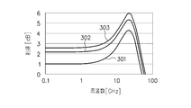
- FIG. 3 is a diagram showing the characteristics of the gain with respect to the frequency of the differential amplifier circuit unit of FIG.
- FIG. 4 is a circuit diagram showing a configuration example of the differential amplifier circuit according to the first embodiment.
- FIG. 5 is a circuit diagram showing a configuration example of the differential amplifier circuit according to the second embodiment.
- FIG. 6 is a circuit diagram showing a configuration example of the differential amplifier circuit according to the third embodiment.
- FIG. 1 is a diagram showing a configuration example of the semiconductor integrated circuit 100 according to the first embodiment.
- the semiconductor integrated circuit 100 has a receiving circuit 101 and an internal circuit 102.
- the receiving circuit 101 includes a terminal circuit 113, a continuous time linear equalizer (CTLE) 114, a determination feedback equalizer (DFE) 115, a clock generator 116, and a display. It has a multiplexer 117 and.
- CLE continuous time linear equalizer
- DFE determination feedback equalizer
- the differential input terminals 111 and 112 receive the differential signal.
- the termination circuit 113 is connected between the differential input terminals 111 and 112.
- the termination circuit 113 is composed of, for example, a resistance element.
- the CTLE 114 continuously performs equivalent processing on the time axis with respect to the differential signals received by the differential input terminals 111 and 112.
- the DFE 115 inputs the output signal of the CTLE 114, and performs equalization processing and binary determination by a feedback loop on the output signal of the CTLE 114.
- the clock generator 116 outputs a clock signal to the DFE 115.
- the demultiplexer 117 inputs the output signal of the DFE 115 and converts the output signal of the DFE 115 from serial data to parallel data.
- the internal circuit 102 processes the output signal of the demultiplexer 117.
- FIG. 2 is a circuit diagram showing a configuration example of the differential amplifier circuit unit in the CTLE 114 of FIG.
- the differential amplifier circuit unit includes current sources 201 and 202, a variable capacitance 203, resistors 204, p-channel field effect transistors 205 and 206, inductors 207 and 208, and resistors 209 and 210.
- the differential amplifier circuit unit amplifies the differential signal input to the differential input terminals Vip and Vin, and outputs the amplified differential signal from the differential output terminals Vop and Von.
- FIG. 3 is a diagram showing the characteristics of the gain with respect to the frequency of the differential amplifier circuit unit of FIG.
- the differential amplifier circuit unit is a high frequency equalizer and has a high gain in the high frequency band.
- the gain characteristic 301 is a characteristic at ⁇ 40 ° C.
- the gain characteristic 302 is a characteristic at 25 ° C.
- the gain characteristic 303 is a characteristic at 125 ° C.
- the gain of the differential amplifier circuit unit fluctuates according to the temperature. If the gain of the differential amplifier circuit unit fluctuates depending on the temperature, it causes a reception error in the reception circuit 101.
- the gain of the differential amplifier circuit unit is preferably constant regardless of the temperature.
- the differential amplifier circuit unit can control the gain in the high frequency band by controlling the value of the variable capacitance 203. Further, the differential amplifier circuit unit can control the DC gain by controlling the value of the resistor 204.
- the resistance value of the resistor 204 is made variable and the value of the resistor 204 is controlled so that the DC gain of the differential amplifier circuit unit becomes constant, the number of parameters for setting the resistance value variably increases. There is a problem that the control becomes complicated and the response speed becomes low.
- a differential amplifier circuit capable of making the DC gain of the differential amplifier circuit unit constant with simple control and at high speed will be described.
- FIG. 4 is a circuit diagram showing a configuration example of the differential amplifier circuit 400 according to the first embodiment.
- the CTLE 114 of FIG. 1 has a differential amplifier circuit 400.
- the differential amplifier circuit 400 includes a differential amplifier circuit unit 401, a replica amplifier circuit unit 402, a p-channel field effect transistor 403, an n-channel field effect transistor 404, and a BGR (bandgap reference) bias generator 405. Have.
- the differential amplifier circuit unit 401 is provided with the p-channel field effect transistors 431 and 432 corresponding to the current sources 201 and 202 in the differential amplifier circuit unit of FIG. 2, and the p-channel field effect transistor corresponding to the resistor 204 is provided. A transistor 433 is provided.
- the differential amplifier circuit unit 401 includes p-channel field-effect transistors 431 to 433, a variable capacitance 203, p-channel field-effect transistors 205 and 206, inductors 207 and 208, and resistors 209 and 210.
- the p-channel field effect transistor 431 is a current source circuit, and the source is connected to the power potential node.
- the p-channel field effect transistor 432 is a current source circuit, the source is connected to the power potential node, and the gate is connected to the gate of the p-channel field effect transistor 431.
- the variable capacitance 203 is connected between the drain of the p-channel field effect transistor 431 and the drain of the p-channel field effect transistor 432.
- the source is connected to the source of the p-channel field-effect transistor 205
- the gate is connected to the output terminal of the operational amplifier 422
- the drain is connected to the source of the p-channel field-effect transistor 206.
- the p-channel field effect transistor 433 receives a control signal output by the operational amplifier 422, and the resistance between the drain and the source changes according to the control signal.
- the source is connected to the drain of the p-channel field-effect transistor 431, the gate is connected to the differential input terminal Vip, and the drain is connected to the differential output terminal Von.
- the source is connected to the drain of the p-channel field-effect transistor 432, the gate is connected to the differential input terminal Vin, and the drain is connected to the differential output terminal Vop.
- the series connection circuit of the inductor 207 and the resistor 209 is a load circuit, and is connected between the drain of the p-channel field effect transistor 205 and the reference potential node.
- the reference potential node is, for example, a ground potential node, which is a node having a lower potential than the power potential node.
- the series connection circuit of the inductor 208 and the resistor 210 is a load circuit, and is connected between the drain of the p-channel field effect transistor 206 and the reference potential node.
- the p-channel field effects 205 and 206 receive differential input signals at the gate differential input terminals Vip and Vin, and generate differential output signals at the drain output terminals Vop and Von.
- the control signal of the gate of the p-channel field-effect transistor 433 by the operational amplifier 422, the resistance between the drain and the source of the p-channel field-effect transistor 433 is controlled, and the DC gain of the differential amplifier circuit unit 401 becomes constant. Be controlled.
- the replica amplifier circuit unit 402 is a replica of the differential amplifier circuit unit 401.
- the replica amplifier circuit unit 402 includes p-channel field effect transistors 411 to 417, resistors 418 to 421, and an operational amplifier 422.
- the p-channel field-effect transistor 412 is a replica transistor of the p-channel field-effect transistor 431, the source is connected to the power potential node, and the gate is connected to the gates of the p-channel field-effect transistors 431 and 432.
- the p-channel field-effect transistor 413 is a replica transistor of the p-channel field-effect transistor 432, the source is connected to the power potential node, and the gate is connected to the gates of the p-channel field-effect transistors 431 and 432.
- the p-channel field-effect transistor 415 is a replica transistor of the p-channel field-effect transistor 433, the source is connected to the source of the p-channel field-effect transistor 416, the gate is connected to the output terminal of the operational amplifier 422, and the drain is the p-channel field effect transistor. It is connected to the source of the effect transistor 417.
- the p-channel field-effect transistor 416 is a replica transistor of the p-channel field-effect transistor 205, and the source is connected to the drain of the p-channel field-effect transistor 412.
- the p-channel field-effect transistor 417 is a replica transistor of the p-channel field-effect transistor 206, and the source is connected to the drain of the p-channel field-effect transistor 413.
- the resistor 419 is a load circuit and is a replica of the resistor 209.
- the resistor 419 is connected between the drain of the p-channel field effect transistor 416 and the reference potential node.
- the resistor 420 is a load circuit and is a replica of the resistor 210.
- the resistor 420 is connected between the drain of the p-channel field effect transistor 417 and the reference potential node.
- the p-channel field effect transistor 411 and the resistor 418 are voltage generation circuits and generate a reference voltage V1.
- the gate of the p-channel field effect transistor 416 receives a reference voltage V1.
- the source is connected to the power potential node
- the gate is connected to the gates of the p-channel field-effect transistors 431 and 432
- the drain is connected to the gate of the p-channel field-effect transistor 416.
- the resistor 418 is connected between the drain of the p-channel field effect transistor 411 and the reference potential node.
- the p-channel field effect transistor 414 and the resistor 421 are voltage generation circuits and generate a reference voltage V2.
- the gate of the p-channel field effect transistor 417 receives a reference voltage V2.
- the source is connected to the power potential node
- the gate is connected to the gates of the p-channel field-effect transistors 431 and 432
- the drain is connected to the gate of the p-channel field-effect transistor 417.
- the resistor 421 is connected between the drain of the p-channel field effect transistor 414 and the reference potential node.
- the-input terminal is connected to the gate of the p-channel field-effect transistor 416
- the + input terminal is connected to the drain of the p-channel field-effect transistor 417
- the output terminal is connected to the gate of the p-channel field-effect transistors 415 and 433. Be connected.
- the source is connected to the power potential node, and the gate and drain are connected to each other.
- the p-channel field-effect transistor 404 has a drain connected to the drain of the p-channel field-effect transistor 403, a gate connected to the BGR bias generator 405, and a source connected to the reference potential node. Further, the gate of the p-channel field-effect transistor 403 is connected to the gate of the p-channel field-effect transistors 431 and 432.
- the BGR bias generator 405 generates a BGR (Band Gap Reference) voltage, and supplies the generated BGR voltage as a bias voltage (second bias voltage) to the gate of the p-channel field effect transistor 404.
- a bias voltage (first bias voltage) for the current source circuit is generated at the gate of the p-channel field-effect transistor 403, and the generated bias voltage is the p-channel field-effect transistor 411 to 414, 431, 432. It is supplied to each gate.
- the p-channel field effect transistors 403, 411 to 414, 431 and 432 are current mirror circuits.
- a current Ib flows through the p-channel field effect transistors 412, 413, 431 and 432.
- a current Ib ⁇ 1/2 whose current amount is 1/2 times that of the current Ib flows through the p-channel field effect transistor 414, for example, by adjusting the transistor size.
- a reference voltage V1 is input to the gate of the p-channel field effect transistor 416.
- a reference voltage V2 is input to the gate of the p-channel electric field effect transistor 417.
- the reference voltages V1 and V2 are different voltages from each other.
- the reference voltage V1 is higher than the reference voltage V2.
- the p-channel field effect transistors 416 and 417 receive reference voltages V1 and V2 at the gate and generate replica output signals V3 and V4 at the drain.
- the replica output signal V3 is a signal of the drain of the p-channel field effect transistor 417.
- the replica output signal V4 is a signal of the drain of the p-channel field effect transistor 416.
- the replica amplifier circuit unit 402 amplifies the differential input signals of the reference voltages V1 and V2, and outputs the differential output signals of the replica output signals V3 and V4. Since the replica amplifier circuit unit 402 does not have a replica of the variable capacitance 203 and the inductors 207 and 208, the gain is substantially constant with respect to the frequency.
- the operational amplifier 422 supplies a control signal to the gates of the p-channel field effect transistors 415 and 433 according to the difference between the replica output signal V3 and the reference voltage V1.
- the operational amplifier 422 generates a control signal so that the gain of the replica amplifier circuit unit 402 becomes constant.
- the operational amplifier 422 may output a control signal according to the difference between the replica output signal V4 and the reference voltage V2.
- the gain of the amplifier circuit unit 401 and the replica amplifier circuit unit 402 fluctuates depending on the temperature. For example, the gains of the amplifier circuit unit 401 and the replica amplifier circuit unit 402 increase, and the signal of the differential output terminal Vop and the replica output signal V3 increase. Then, the difference between the replica output signal V3 and the reference voltage V1 becomes large, and the control signal output by the operational amplifier 422 rises. Then, the resistance between the drain and the source of the p-channel field effect transistor 415 increases, and the gain of the replica amplifier circuit unit 402 decreases. As a result, the replica output signal V3 drops. By the above control, the operational amplifier 422 generates a control signal so that the gain of the replica amplifier circuit unit 402 becomes constant.
- the resistance between the drain and the source of the p-channel field effect transistor 433 increases, and the gain of the differential amplifier circuit unit 401 decreases. As a result, the signal of the differential output terminal Vop drops.
- the DC gain of the amplifier circuit unit 401 is controlled to be constant regardless of the temperature.
- the direct current gain of the differential amplifier circuit unit 401 can be made constant by simple control. Further, since the differential amplifier circuit unit 401 controls the gain of DC by using the p-channel field effect transistor 433, there is no element to be additionally connected to the pair of input nodes Vip and Vin, and the input load is increased. Since it does not increase, the high speed of operation can be maintained in the differential amplifier circuit 400.
- FIG. 5 is a circuit diagram showing a configuration example of the differential amplifier circuit 500 according to the second embodiment.
- the CTLE 114 of FIG. 1 has a differential amplifier circuit 500.
- the differential amplifier circuit 500 provides the differential amplifier circuit 400 of FIG. 4 with an n-channel field-effect transistor instead of the p-channel field-effect transistor and a p-channel field-effect transistor instead of the n-channel field-effect transistor. It is a transistor.
- the differential amplifier circuit 500 includes a differential amplifier circuit unit 501, a replica amplifier circuit unit 502, an n-channel field effect transistor 503, a p-channel field effect transistor 504, and a BGR bias generator 405.
- the differential amplifier circuit unit 501 includes n-channel field-effect transistors 531 to 533, variable capacitance 203, n-channel field-effect transistors 534 and 535, inductors 207 and 208, and resistors 209 and 210.
- the n-channel field effect transistor 531 is a current source circuit, and the source is connected to the reference potential node.
- the n-channel field-effect transistor 532 is a current source circuit in which the source is connected to the reference potential node and the gate is connected to the gate of the n-channel field-effect transistor 531.
- the variable capacitance 203 is connected between the drain of the n-channel field-effect transistor 531 and the drain of the n-channel field-effect transistor 532.
- the source is connected to the source of the n-channel field-effect transistor 535
- the gate is connected to the output terminal of the operational amplifier 422
- the drain is connected to the source of the n-channel field-effect transistor 534.
- the n-channel field effect transistor 533 receives a control signal output from the operational amplifier 422 at the gate, and the resistance between the drain and the source changes according to the control signal.
- the series connection circuit of the inductor 207 and the resistor 209 is a load circuit, and is connected between the drain of the n-channel field effect transistor 534 and the power potential node.
- the series connection circuit of the inductor 208 and the resistor 210 is a load circuit, and is connected between the drain of the n-channel field effect transistor 535 and the power potential node.
- the n-channel field effects 534 and 535 receive the differential input signal at the gate differential input terminals Vip and Vin, and generate the differential output signal at the drain output terminals Vop and Von.
- the control signal of the gate of the n-channel field-effect transistor 533 by the operational amplifier 422, the resistance between the drain and the source of the n-channel field-effect transistor 533 is controlled, and the DC gain of the differential amplifier circuit unit 501 becomes constant. Be controlled.
- the replica amplifier circuit unit 502 is a replica of the differential amplifier circuit unit 501.
- the replica amplifier circuit unit 502 includes n-channel field effect transistors 511 to 517, resistors 418 to 421, and an operational amplifier 422.
- the n-channel field-effect transistor 512 is a replica transistor of the n-channel field-effect transistor 531.
- the source is connected to the reference potential node, and the gate is connected to the gates of the n-channel field-effect transistors 531 and 532.
- the n-channel field-effect transistor 513 is a replica transistor of the n-channel field-effect transistor 532, with the source connected to the reference potential node and the gate connected to the gates of the n-channel field-effect transistors 531 and 532.
- the n-channel field-effect transistor 515 is a replica transistor of the n-channel field-effect transistor 533, the source is connected to the source of the n-channel field-effect transistor 517, the gate is connected to the output terminal of the operational amplifier 422, and the drain is the n-channel field effect transistor. It is connected to the source of the effect transistor 516.
- the n-channel field-effect transistor 516 is a replica transistor of the n-channel field-effect transistor 534, and the source is connected to the drain of the n-channel field-effect transistor 512.
- the n-channel field-effect transistor 517 is a replica transistor of the n-channel field-effect transistor 535, and the source is connected to the drain of the n-channel field-effect transistor 513.
- the resistor 419 is a load circuit and is a replica of the resistor 209.
- the resistor 419 is connected between the drain of the n-channel field effect transistor 516 and the power potential node.
- the resistor 420 is a load circuit and is a replica of the resistor 210.
- the resistor 420 is connected between the drain of the n-channel field effect transistor 517 and the power potential node.
- the n-channel field effect transistor 511 and the resistor 418 are voltage generation circuits and generate a reference voltage V1.
- the gate of the n-channel field effect transistor 516 receives a reference voltage V1.
- the source is connected to the reference potential node
- the gate is connected to the gates of the n-channel field-effect transistors 531 and 532
- the drain is connected to the gate of the n-channel field-effect transistor 516.
- the resistor 418 is connected between the drain of the n-channel field effect transistor 511 and the power potential node.
- the n-channel field effect transistor 514 and the resistor 421 are voltage generation circuits and generate a reference voltage V2.
- the gate of the n-channel field effect transistor 517 receives a reference voltage V2.
- the source is connected to the reference potential node
- the gate is connected to the gates of the n-channel field-effect transistors 531 and 532
- the drain is connected to the gate of the n-channel field-effect transistor 517.
- the resistor 421 is connected between the drain of the n-channel field effect transistor 514 and the power potential node.
- the-input terminal is connected to the gate of the n-channel field-effect transistor 516
- the + input terminal is connected to the drain of the n-channel field-effect transistor 517
- the output terminal is connected to the gate of the n-channel field-effect transistors 515 and 533. Be connected.
- the source is connected to the reference potential node, and the gate and drain are connected to the gate of the n-channel field-effect transistor 514.
- the drain is connected to the drain of the n-channel field effect transistor 503
- the gate is connected to the BGR bias generator 405, and the source is connected to the power potential node.
- the BGR bias generator 405 generates a BGR voltage and supplies the generated BGR voltage as a bias voltage (third bias voltage) to the n-channel field effect transistor 504 gate.
- a bias voltage (first bias voltage) for the current source circuit is generated at the gate of the n-channel field-effect transistor 503, and the generated bias voltage is the n-channel field-effect transistor 511 to 514, 513, 532. It is supplied to each gate.
- the n-channel field effect transistors 503, 511 to 514, 513 and 532 are current mirror circuits.
- a current Ib flows through the n-channel field effect transistors 512, 513, 513 and 532.
- a current Ib ⁇ 3/2 flows through the n-channel field effect transistor 511.
- a current Ib ⁇ 1/2 flows through the n-channel field effect transistor 514.
- a reference voltage V1 is input to the gate of the n-channel field effect transistor 516.
- a reference voltage V2 is input to the gate of the n-channel field effect transistor 517.
- the reference voltages V1 and V2 are different voltages from each other.
- the reference voltage V1 is lower than the reference voltage V2.
- the n-channel field effect transistors 516 and 517 receive reference voltages V1 and V2 at the gate and generate replica output signals V3 and V4 at the drain.
- the replica output signal V3 is a signal of the drain of the n-channel field effect transistor 517.
- the replica output signal V4 is a signal of the drain of the n-channel field effect transistor 516.
- the replica amplifier circuit unit 502 amplifies the differential input signals of the reference voltages V1 and V2, and outputs the differential output signals of the replica output signals V3 and V4. Since the replica amplifier circuit unit 502 does not have a replica of the variable capacitance 203 and the inductors 207 and 208, the gain is substantially constant with respect to the frequency.
- the operational amplifier 422 supplies a control signal to the gates of the n-channel field effect transistors 515 and 533 according to the difference between the replica output signal V3 and the reference voltage V1.
- the operational amplifier 422 generates a control signal so that the gain of the replica amplifier circuit unit 502 becomes constant.
- the operational amplifier 422 may output a control signal according to the difference between the replica output signal V4 and the reference voltage V2.
- the gains of the amplifier circuit unit 501 and the replica amplifier circuit unit 502 vary depending on the temperature. For example, the gains of the amplifier circuit unit 501 and the replica amplifier circuit unit 502 decrease, and the signal of the differential output terminal Vop and the replica output signal V3 increase. Then, the difference between the replica output signal V3 and the reference voltage V1 becomes large, and the control signal output by the operational amplifier 422 rises. Then, the resistance between the drain and the source of the n-channel field effect transistor 515 becomes low, and the gain of the replica amplifier circuit unit 502 increases. As a result, the replica output signal V3 drops. By the above control, the operational amplifier 422 generates a control signal so that the gain of the replica amplifier circuit unit 502 becomes constant.
- the resistance between the drain and source of the n-channel field effect transistor 533 decreases, and the gain of the differential amplifier circuit unit 501 increases. As a result, the signal of the differential output terminal Vop drops.
- the DC gain of the amplifier circuit unit 501 is controlled to be constant regardless of the temperature.
- the direct current gain of the differential amplifier circuit unit 501 can be made constant by simple control. Further, since the differential amplifier circuit unit 501 controls the gain of DC by using the n-channel field effect transistor 533, there is no element to be additionally connected to the pair of input nodes Vip and Vin, and the input load is increased. Since it does not increase, the high speed of operation can be maintained in the differential amplifier circuit 500.
- FIG. 6 is a circuit diagram showing a configuration example of the differential amplifier circuit 400 according to the third embodiment.
- the differential amplifier circuit 400 of FIG. 6 is obtained by removing the variable capacitance 203 and the inductors 207 and 208 from the differential amplifier circuit 400 of FIG.
- the resistor 209 is a load circuit and is connected between the drain of the p-channel field effect transistor 205 and the reference potential node.
- the resistor 210 is a load circuit and is connected between the drain of the p-channel field effect transistor 206 and the reference potential node.
- the gain of the differential amplifier circuit unit 401 becomes substantially constant with respect to the frequency.
- the operational amplifier 422 generates a control signal so that the gains of the differential amplifier circuit unit 401 and the replica amplifier circuit unit 402 are constant regardless of the temperature. ..
- the gain of the differential amplifier circuit unit 401 can be made constant by simple control.
- the differential amplifier circuit unit 401 controls the gain of DC by using the p-channel field effect transistor 433, there is no element to be additionally connected to the pair of input nodes Vip and Vin, and the input load is increased. Since it does not increase, the high speed of operation can be maintained in the differential amplifier circuit 400.
- variable capacitance 203 and the inductors 207 and 208 can be deleted.
- the gain of the differential amplifier circuit unit can be made constant while maintaining the high speed of operation with simple control.
Landscapes
- Engineering & Computer Science (AREA)
- Power Engineering (AREA)
- Computer Networks & Wireless Communication (AREA)
- Signal Processing (AREA)
- Microelectronics & Electronic Packaging (AREA)
- Amplifiers (AREA)
- Control Of Amplification And Gain Control (AREA)
Priority Applications (4)
| Application Number | Priority Date | Filing Date | Title |
|---|---|---|---|
| JP2021565208A JP7453562B2 (ja) | 2019-12-17 | 2019-12-17 | 差動増幅回路、受信回路及び半導体集積回路 |
| PCT/JP2019/049423 WO2021124450A1 (ja) | 2019-12-17 | 2019-12-17 | 差動増幅回路、受信回路及び半導体集積回路 |
| CN201980102950.6A CN114788174B (zh) | 2019-12-17 | 2019-12-17 | 差动放大电路、接收电路以及半导体集成电路 |
| US17/836,709 US12113494B2 (en) | 2019-12-17 | 2022-06-09 | Differential amplifier circuit, reception circuit, and semiconductor integrated circuit |
Applications Claiming Priority (1)
| Application Number | Priority Date | Filing Date | Title |
|---|---|---|---|
| PCT/JP2019/049423 WO2021124450A1 (ja) | 2019-12-17 | 2019-12-17 | 差動増幅回路、受信回路及び半導体集積回路 |
Related Child Applications (1)
| Application Number | Title | Priority Date | Filing Date |
|---|---|---|---|
| US17/836,709 Continuation US12113494B2 (en) | 2019-12-17 | 2022-06-09 | Differential amplifier circuit, reception circuit, and semiconductor integrated circuit |
Publications (1)
| Publication Number | Publication Date |
|---|---|
| WO2021124450A1 true WO2021124450A1 (ja) | 2021-06-24 |
Family
ID=76477285
Family Applications (1)
| Application Number | Title | Priority Date | Filing Date |
|---|---|---|---|
| PCT/JP2019/049423 Ceased WO2021124450A1 (ja) | 2019-12-17 | 2019-12-17 | 差動増幅回路、受信回路及び半導体集積回路 |
Country Status (4)
| Country | Link |
|---|---|
| US (1) | US12113494B2 (https=) |
| JP (1) | JP7453562B2 (https=) |
| CN (1) | CN114788174B (https=) |
| WO (1) | WO2021124450A1 (https=) |
Cited By (1)
| Publication number | Priority date | Publication date | Assignee | Title |
|---|---|---|---|---|
| JPWO2021250870A1 (https=) * | 2020-06-11 | 2021-12-16 |
Citations (4)
| Publication number | Priority date | Publication date | Assignee | Title |
|---|---|---|---|---|
| US20090015328A1 (en) * | 2007-07-11 | 2009-01-15 | Axiom Microdevices, Inc. | Low offset envelope detector and method of use |
| JP2010034733A (ja) * | 2008-07-28 | 2010-02-12 | Kawasaki Microelectronics Inc | スケルチ検出回路 |
| US20110001562A1 (en) * | 2009-07-06 | 2011-01-06 | Young-Soo Sohn | High speed linear differential amplifier |
| JP2017538363A (ja) * | 2014-12-15 | 2017-12-21 | ノルディック セミコンダクタ アーエスアーNordic Semiconductor ASA | 差動増幅器 |
Family Cites Families (11)
| Publication number | Priority date | Publication date | Assignee | Title |
|---|---|---|---|---|
| JP4682419B2 (ja) | 2000-12-22 | 2011-05-11 | 日本テキサス・インスツルメンツ株式会社 | 可変利得増幅回路 |
| US6529077B1 (en) * | 2001-08-22 | 2003-03-04 | Institute Of Microelectronics | Gain compensation circuit for CMOS amplifiers |
| US7116088B2 (en) * | 2003-06-09 | 2006-10-03 | Silicon Storage Technology, Inc. | High voltage shunt regulator for flash memory |
| JP2005151460A (ja) * | 2003-11-19 | 2005-06-09 | Toyota Industries Corp | Am中間周波可変利得増幅回路、可変利得増幅回路及びその半導体集積回路 |
| US7394310B2 (en) * | 2004-08-31 | 2008-07-01 | Broadcom Corporation | System and method for programmable switching characteristics of an analog switch in a transconductance amplifier |
| US7911244B2 (en) * | 2007-11-30 | 2011-03-22 | Sony Corporation | Differential drive circuit and communication device |
| JP2010141589A (ja) * | 2008-12-11 | 2010-06-24 | Elpida Memory Inc | 差動増幅回路 |
| US7728630B1 (en) * | 2009-01-29 | 2010-06-01 | Xilinx, Inc. | Method and apparatus for a process, voltage, and temperature variation tolerant semiconductor device |
| US8823450B2 (en) * | 2012-07-19 | 2014-09-02 | Honeywell International Inc. | Multiple-output transconductance amplifier based instrumentation amplifier |
| JP2018522490A (ja) | 2015-07-29 | 2018-08-09 | メイコム コネクティビティ ソリューションズ,エルエルシーMacom Connectivity Solutions,Llc | 制御された利得ステップを有するプログラム可能な利得増幅器 |
| US20230308065A1 (en) * | 2022-03-24 | 2023-09-28 | Kandou Labs SA | Variable gain amplifier biased with a fixed current to improve low-gain linearity |
-
2019
- 2019-12-17 CN CN201980102950.6A patent/CN114788174B/zh active Active
- 2019-12-17 JP JP2021565208A patent/JP7453562B2/ja active Active
- 2019-12-17 WO PCT/JP2019/049423 patent/WO2021124450A1/ja not_active Ceased
-
2022
- 2022-06-09 US US17/836,709 patent/US12113494B2/en active Active
Patent Citations (4)
| Publication number | Priority date | Publication date | Assignee | Title |
|---|---|---|---|---|
| US20090015328A1 (en) * | 2007-07-11 | 2009-01-15 | Axiom Microdevices, Inc. | Low offset envelope detector and method of use |
| JP2010034733A (ja) * | 2008-07-28 | 2010-02-12 | Kawasaki Microelectronics Inc | スケルチ検出回路 |
| US20110001562A1 (en) * | 2009-07-06 | 2011-01-06 | Young-Soo Sohn | High speed linear differential amplifier |
| JP2017538363A (ja) * | 2014-12-15 | 2017-12-21 | ノルディック セミコンダクタ アーエスアーNordic Semiconductor ASA | 差動増幅器 |
Cited By (2)
| Publication number | Priority date | Publication date | Assignee | Title |
|---|---|---|---|---|
| JPWO2021250870A1 (https=) * | 2020-06-11 | 2021-12-16 | ||
| JP7567909B2 (ja) | 2020-06-11 | 2024-10-16 | 株式会社ソシオネクスト | 増幅回路、差動増幅回路、受信回路及び半導体集積回路 |
Also Published As
| Publication number | Publication date |
|---|---|
| CN114788174A (zh) | 2022-07-22 |
| JPWO2021124450A1 (https=) | 2021-06-24 |
| US12113494B2 (en) | 2024-10-08 |
| JP7453562B2 (ja) | 2024-03-21 |
| US20220302889A1 (en) | 2022-09-22 |
| CN114788174B (zh) | 2025-04-22 |
Similar Documents
| Publication | Publication Date | Title |
|---|---|---|
| CN108886346B (zh) | 用于经由副本电路和反馈控制来控制共模电压的系统和方法 | |
| US9746864B1 (en) | Fast transient low drop-out voltage regulator for a voltage-mode driver | |
| TWI535225B (zh) | 接收器,及接收器前端電路 | |
| CN101447785B (zh) | 差分驱动电路和通信设备 | |
| US9685914B2 (en) | Amplifier circuit | |
| US10523165B2 (en) | Common mode feedback circuit with backgate control | |
| WO2018026578A1 (en) | Impedance and swing control for voltage-mode driver | |
| JP2009105810A (ja) | 増幅装置及びバイアス回路 | |
| CN113259279B (zh) | 一种均衡器 | |
| WO2017083052A2 (en) | Variable gain amplifier with improved power supply noise rejection | |
| US8400214B2 (en) | Class AB output stage | |
| US20230361735A1 (en) | Common adjustment circuit | |
| JP7453562B2 (ja) | 差動増幅回路、受信回路及び半導体集積回路 | |
| JPWO2022162943A5 (https=) | ||
| US9998120B1 (en) | Circuit for and method of shifting a high range input common mode voltage | |
| US10122337B2 (en) | Programmable gain amplifier | |
| US7453104B2 (en) | Operational amplifier including low DC gain wideband feed forward circuit and high DC gain narrowband gain circuit | |
| CN108781062B (zh) | 可变增益放大器 | |
| US9531326B2 (en) | Limiting amplifiers | |
| KR100668455B1 (ko) | 가변 이득 증폭기 | |
| KR100801563B1 (ko) | 가변 이득 증폭기 | |
| US7417483B2 (en) | Wide-band wide-swing CMOS gain enhancement technique and method therefor | |
| CN119363097A (zh) | 单端至差分信号转换电路及方法 | |
| Madian et al. | Low Voltage CMOS Fully Differential Current Feedback Amplifier with Controllable 3-dB Bandwidth | |
| WO2004098044A1 (en) | High speed high gain amplifier |
Legal Events
| Date | Code | Title | Description |
|---|---|---|---|
| 121 | Ep: the epo has been informed by wipo that ep was designated in this application |
Ref document number: 19956928 Country of ref document: EP Kind code of ref document: A1 |
|
| ENP | Entry into the national phase |
Ref document number: 2021565208 Country of ref document: JP Kind code of ref document: A |
|
| NENP | Non-entry into the national phase |
Ref country code: DE |
|
| 122 | Ep: pct application non-entry in european phase |
Ref document number: 19956928 Country of ref document: EP Kind code of ref document: A1 |
|
| WWG | Wipo information: grant in national office |
Ref document number: 201980102950.6 Country of ref document: CN |