WO2021095603A1 - 画像表示装置の製造方法および画像表示装置 - Google Patents
画像表示装置の製造方法および画像表示装置 Download PDFInfo
- Publication number
- WO2021095603A1 WO2021095603A1 PCT/JP2020/041208 JP2020041208W WO2021095603A1 WO 2021095603 A1 WO2021095603 A1 WO 2021095603A1 JP 2020041208 W JP2020041208 W JP 2020041208W WO 2021095603 A1 WO2021095603 A1 WO 2021095603A1
- Authority
- WO
- WIPO (PCT)
- Prior art keywords
- light emitting
- layer
- insulating film
- image display
- plug
- Prior art date
- Legal status (The legal status is an assumption and is not a legal conclusion. Google has not performed a legal analysis and makes no representation as to the accuracy of the status listed.)
- Ceased
Links
Images




























Classifications
-
- H—ELECTRICITY
- H10—SEMICONDUCTOR DEVICES; ELECTRIC SOLID-STATE DEVICES NOT OTHERWISE PROVIDED FOR
- H10H—INORGANIC LIGHT-EMITTING SEMICONDUCTOR DEVICES HAVING POTENTIAL BARRIERS
- H10H29/00—Integrated devices, or assemblies of multiple devices, comprising at least one light-emitting semiconductor element covered by group H10H20/00
- H10H29/10—Integrated devices comprising at least one light-emitting semiconductor component covered by group H10H20/00
- H10H29/14—Integrated devices comprising at least one light-emitting semiconductor component covered by group H10H20/00 comprising multiple light-emitting semiconductor components
- H10H29/142—Two-dimensional arrangements, e.g. asymmetric LED layout
-
- G—PHYSICS
- G09—EDUCATION; CRYPTOGRAPHY; DISPLAY; ADVERTISING; SEALS
- G09F—DISPLAYING; ADVERTISING; SIGNS; LABELS OR NAME-PLATES; SEALS
- G09F9/00—Indicating arrangements for variable information in which the information is built-up on a support by selection or combination of individual elements
-
- G—PHYSICS
- G09—EDUCATION; CRYPTOGRAPHY; DISPLAY; ADVERTISING; SEALS
- G09F—DISPLAYING; ADVERTISING; SIGNS; LABELS OR NAME-PLATES; SEALS
- G09F9/00—Indicating arrangements for variable information in which the information is built-up on a support by selection or combination of individual elements
- G09F9/30—Indicating arrangements for variable information in which the information is built-up on a support by selection or combination of individual elements in which the desired character or characters are formed by combining individual elements
-
- G—PHYSICS
- G09—EDUCATION; CRYPTOGRAPHY; DISPLAY; ADVERTISING; SEALS
- G09F—DISPLAYING; ADVERTISING; SIGNS; LABELS OR NAME-PLATES; SEALS
- G09F9/00—Indicating arrangements for variable information in which the information is built-up on a support by selection or combination of individual elements
- G09F9/30—Indicating arrangements for variable information in which the information is built-up on a support by selection or combination of individual elements in which the desired character or characters are formed by combining individual elements
- G09F9/33—Indicating arrangements for variable information in which the information is built-up on a support by selection or combination of individual elements in which the desired character or characters are formed by combining individual elements being semiconductor devices, e.g. diodes
-
- H—ELECTRICITY
- H10—SEMICONDUCTOR DEVICES; ELECTRIC SOLID-STATE DEVICES NOT OTHERWISE PROVIDED FOR
- H10H—INORGANIC LIGHT-EMITTING SEMICONDUCTOR DEVICES HAVING POTENTIAL BARRIERS
- H10H20/00—Individual inorganic light-emitting semiconductor devices having potential barriers, e.g. light-emitting diodes [LED]
- H10H20/01—Manufacture or treatment
- H10H20/011—Manufacture or treatment of bodies, e.g. forming semiconductor layers
- H10H20/013—Manufacture or treatment of bodies, e.g. forming semiconductor layers having light-emitting regions comprising only Group III-V materials
- H10H20/0133—Manufacture or treatment of bodies, e.g. forming semiconductor layers having light-emitting regions comprising only Group III-V materials with a substrate not being Group III-V materials
- H10H20/01335—Manufacture or treatment of bodies, e.g. forming semiconductor layers having light-emitting regions comprising only Group III-V materials with a substrate not being Group III-V materials the light-emitting regions comprising nitride materials
-
- H—ELECTRICITY
- H10—SEMICONDUCTOR DEVICES; ELECTRIC SOLID-STATE DEVICES NOT OTHERWISE PROVIDED FOR
- H10H—INORGANIC LIGHT-EMITTING SEMICONDUCTOR DEVICES HAVING POTENTIAL BARRIERS
- H10H20/00—Individual inorganic light-emitting semiconductor devices having potential barriers, e.g. light-emitting diodes [LED]
- H10H20/01—Manufacture or treatment
- H10H20/011—Manufacture or treatment of bodies, e.g. forming semiconductor layers
- H10H20/018—Bonding of wafers
-
- H—ELECTRICITY
- H10—SEMICONDUCTOR DEVICES; ELECTRIC SOLID-STATE DEVICES NOT OTHERWISE PROVIDED FOR
- H10H—INORGANIC LIGHT-EMITTING SEMICONDUCTOR DEVICES HAVING POTENTIAL BARRIERS
- H10H20/00—Individual inorganic light-emitting semiconductor devices having potential barriers, e.g. light-emitting diodes [LED]
- H10H20/80—Constructional details
- H10H20/81—Bodies
- H10H20/819—Bodies characterised by their shape, e.g. curved or truncated substrates
- H10H20/82—Roughened surfaces, e.g. at the interface between epitaxial layers
-
- H—ELECTRICITY
- H10—SEMICONDUCTOR DEVICES; ELECTRIC SOLID-STATE DEVICES NOT OTHERWISE PROVIDED FOR
- H10H—INORGANIC LIGHT-EMITTING SEMICONDUCTOR DEVICES HAVING POTENTIAL BARRIERS
- H10H20/00—Individual inorganic light-emitting semiconductor devices having potential barriers, e.g. light-emitting diodes [LED]
- H10H20/80—Constructional details
- H10H20/85—Packages
- H10H20/857—Interconnections, e.g. lead-frames, bond wires or solder balls
-
- H—ELECTRICITY
- H10—SEMICONDUCTOR DEVICES; ELECTRIC SOLID-STATE DEVICES NOT OTHERWISE PROVIDED FOR
- H10H—INORGANIC LIGHT-EMITTING SEMICONDUCTOR DEVICES HAVING POTENTIAL BARRIERS
- H10H20/00—Individual inorganic light-emitting semiconductor devices having potential barriers, e.g. light-emitting diodes [LED]
- H10H20/80—Constructional details
- H10H20/81—Bodies
-
- H—ELECTRICITY
- H10—SEMICONDUCTOR DEVICES; ELECTRIC SOLID-STATE DEVICES NOT OTHERWISE PROVIDED FOR
- H10H—INORGANIC LIGHT-EMITTING SEMICONDUCTOR DEVICES HAVING POTENTIAL BARRIERS
- H10H20/00—Individual inorganic light-emitting semiconductor devices having potential barriers, e.g. light-emitting diodes [LED]
- H10H20/80—Constructional details
- H10H20/81—Bodies
- H10H20/822—Materials of the light-emitting regions
- H10H20/824—Materials of the light-emitting regions comprising only Group III-V materials, e.g. GaP
- H10H20/825—Materials of the light-emitting regions comprising only Group III-V materials, e.g. GaP containing nitrogen, e.g. GaN
-
- H—ELECTRICITY
- H10—SEMICONDUCTOR DEVICES; ELECTRIC SOLID-STATE DEVICES NOT OTHERWISE PROVIDED FOR
- H10H—INORGANIC LIGHT-EMITTING SEMICONDUCTOR DEVICES HAVING POTENTIAL BARRIERS
- H10H20/00—Individual inorganic light-emitting semiconductor devices having potential barriers, e.g. light-emitting diodes [LED]
- H10H20/80—Constructional details
- H10H20/85—Packages
- H10H20/851—Wavelength conversion means
-
- H—ELECTRICITY
- H10—SEMICONDUCTOR DEVICES; ELECTRIC SOLID-STATE DEVICES NOT OTHERWISE PROVIDED FOR
- H10H—INORGANIC LIGHT-EMITTING SEMICONDUCTOR DEVICES HAVING POTENTIAL BARRIERS
- H10H20/00—Individual inorganic light-emitting semiconductor devices having potential barriers, e.g. light-emitting diodes [LED]
- H10H20/80—Constructional details
- H10H20/85—Packages
- H10H20/855—Optical field-shaping means, e.g. lenses
- H10H20/856—Reflecting means
-
- H—ELECTRICITY
- H10—SEMICONDUCTOR DEVICES; ELECTRIC SOLID-STATE DEVICES NOT OTHERWISE PROVIDED FOR
- H10W—GENERIC PACKAGES, INTERCONNECTIONS, CONNECTORS OR OTHER CONSTRUCTIONAL DETAILS OF DEVICES COVERED BY CLASS H10
- H10W70/00—Package substrates; Interposers; Redistribution layers [RDL]
- H10W70/01—Manufacture or treatment
- H10W70/05—Manufacture or treatment of insulating or insulated package substrates, or of interposers, or of redistribution layers
- H10W70/093—Connecting or disconnecting other interconnections thereto or therefrom, e.g. connecting bond wires or bumps
-
- H—ELECTRICITY
- H10—SEMICONDUCTOR DEVICES; ELECTRIC SOLID-STATE DEVICES NOT OTHERWISE PROVIDED FOR
- H10W—GENERIC PACKAGES, INTERCONNECTIONS, CONNECTORS OR OTHER CONSTRUCTIONAL DETAILS OF DEVICES COVERED BY CLASS H10
- H10W70/00—Package substrates; Interposers; Redistribution layers [RDL]
- H10W70/60—Insulating or insulated package substrates; Interposers; Redistribution layers
-
- H—ELECTRICITY
- H10—SEMICONDUCTOR DEVICES; ELECTRIC SOLID-STATE DEVICES NOT OTHERWISE PROVIDED FOR
- H10W—GENERIC PACKAGES, INTERCONNECTIONS, CONNECTORS OR OTHER CONSTRUCTIONAL DETAILS OF DEVICES COVERED BY CLASS H10
- H10W90/00—Package configurations
-
- H—ELECTRICITY
- H10—SEMICONDUCTOR DEVICES; ELECTRIC SOLID-STATE DEVICES NOT OTHERWISE PROVIDED FOR
- H10W—GENERIC PACKAGES, INTERCONNECTIONS, CONNECTORS OR OTHER CONSTRUCTIONAL DETAILS OF DEVICES COVERED BY CLASS H10
- H10W90/00—Package configurations
- H10W90/10—Configurations of laterally-adjacent chips
-
- H—ELECTRICITY
- H10—SEMICONDUCTOR DEVICES; ELECTRIC SOLID-STATE DEVICES NOT OTHERWISE PROVIDED FOR
- H10W—GENERIC PACKAGES, INTERCONNECTIONS, CONNECTORS OR OTHER CONSTRUCTIONAL DETAILS OF DEVICES COVERED BY CLASS H10
- H10W90/00—Package configurations
- H10W90/20—Configurations of stacked chips
- H10W90/22—Configurations of stacked chips the stacked chips being on both top and bottom sides of a package substrate, interposer or RDL
-
- H—ELECTRICITY
- H10—SEMICONDUCTOR DEVICES; ELECTRIC SOLID-STATE DEVICES NOT OTHERWISE PROVIDED FOR
- H10W—GENERIC PACKAGES, INTERCONNECTIONS, CONNECTORS OR OTHER CONSTRUCTIONAL DETAILS OF DEVICES COVERED BY CLASS H10
- H10W90/00—Package configurations
- H10W90/701—Package configurations characterised by the relative positions of pads or connectors relative to package parts
- H10W90/791—Package configurations characterised by the relative positions of pads or connectors relative to package parts of direct-bonded pads
- H10W90/792—Package configurations characterised by the relative positions of pads or connectors relative to package parts of direct-bonded pads between multiple chips
Definitions
- An embodiment of the present invention relates to a method for manufacturing an image display device and an image display device.
- a display device using a micro LED which is a fine light emitting element
- a method of manufacturing a display device using micro LEDs a method of sequentially transferring individually formed micro LEDs to a drive circuit has been introduced.
- the number of micro LED elements increases as the image quality becomes higher, such as full high definition, 4K, 8K, etc.
- the transfer process requires a huge amount of time. Further, a poor connection between the micro LED and the drive circuit or the like may occur, resulting in a decrease in yield.
- a technique is known in which a semiconductor layer including a light emitting layer is grown on a Si substrate, electrodes are formed on the semiconductor layer, and then the electrodes are attached to a circuit board on which a drive circuit is formed (for example, Patent Document 1).
- One embodiment of the present invention provides a method for manufacturing an image display device that shortens the transfer process of a light emitting element and improves the yield.
- the method for manufacturing an image display device includes a step of preparing a second substrate in which a semiconductor layer including a light emitting layer is grown on a first substrate, and a circuit formed on the translucent substrate.
- the step of forming the first metal layer formed above and connected to the first wiring layer, the second substrate is bonded to the third substrate, and the first metal layer is electrically connected to the semiconductor layer.
- the step of etching the semiconductor layer to form a light emitting element the step of etching the first metal layer to form a plug electrically connected to the light emitting element, and the plug and the light emitting.
- the method for manufacturing an image display device includes a step of preparing a second substrate in which a semiconductor layer including a light emitting layer is grown on a first substrate, and a method of forming the image display device on the translucent substrate.
- a step of exposing a light emitting surface facing the surface of the light emitting element on the side of the first insulating film and a step of forming a second wiring layer electrically connected to the light emitting surface are provided.
- the image display device includes a translucent substrate having a first surface, a circuit element provided on the first surface, and electricity provided on the circuit element.
- a first wiring layer that is specifically connected, a first insulating film that covers the circuit element and the first wiring layer on the first surface, and a first insulating film provided on the first insulating film and connected to the first wiring layer.
- a first light emitting element provided on the first plug and electrically connected to the first plug, and having a light emitting surface on a surface facing the side surface of the first insulating film.
- a second wiring layer connected to the above is provided.
- the image display device includes a flexible substrate having a first surface, a circuit element provided on the first surface, and the circuit element provided on the circuit element.
- a first wiring layer electrically connected to the first wiring layer, a first insulating film that covers the circuit element and the first wiring layer on the first surface, and the first wiring layer provided on the first insulating film.
- a first light emitting surface provided on the first plug and electrically connected to the first plug, and having a light emitting surface on a surface facing the surface on the side of the first insulating film.
- An element at least a part of the first light emitting element, a second insulating film covering the first insulating film and the first plug, and a light emitting surface of the first light emitting element provided on the second insulating film. It includes an electrically connected second wiring layer.
- the image display device includes a translucent substrate having a first surface, a plurality of transistors provided on the first surface, and the plurality of transistors provided on the plurality of transistors.
- a first wiring layer electrically connected to a transistor, a first insulating film covering the plurality of transistors and the first wiring layer on the first surface, and the first insulating film provided on the first insulating film.
- a plug connected to the wiring layer, a first conductive type first semiconductor layer provided on the plug and electrically connected to the plug, and a light emitting layer provided on the first semiconductor layer.
- the second semiconductor layer of the second conductive type which is provided on the light emitting layer and is different from the first conductive type, and the plug, the first insulating film, the light emitting layer and the first semiconductor layer are covered and the first.
- a method for manufacturing an image display device that shortens the transfer process of the light emitting element and improves the yield is realized.
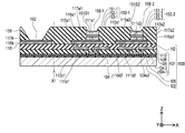
- FIG. 1 is a schematic cross-sectional view illustrating a part of the image display device according to the embodiment.
- the pixels that make up the image displayed on the image display device are made up of a plurality of subpixels.
- FIG. 1 schematically shows the configuration of subpixels 20-1 and 20-2 of the image display device of the present embodiment.
- Subpixels 20-1 and 20-2 are arranged on a two-dimensional plane together with other subpixels. Let the two-dimensional plane in which the subpixels 20-1 and 20-2 are arranged be the XY plane. A plurality of subpixels including the subpixels 20-1 and 20-2 are arranged along the X-axis direction and the Y-axis direction.
- FIG. 1 schematically shows a cross section when subpixels 20-1 and 20-2 are cut along a plane parallel to the XZ plane.
- Subpixel 20-1 has a light emitting surface 151S1 substantially parallel to the XY plane.
- Subpixel 20-2 has a light emitting surface 151S2 substantially parallel to the XY plane.
- These light emitting surfaces 151S1 and 151S2 mainly emit light in the positive direction of the Z axis orthogonal to the XY plane.
- the subpixel 20-1 of the image display device of the present embodiment includes a transistor 103-1, a light emitting element 150-1, and a plug 116a1.
- Subpixel 20-2 includes a transistor 103-2, a light emitting element 150-2, and a plug 116a2.
- Subpixels 20-1 and 20-2 include a substrate 102, a first wiring layer 110, a first interlayer insulating film 112, a second interlayer insulating film 156, and a second wiring layer 159. Includes.
- the substrate 102, the first wiring layer 110, the second wiring layer 159, the first interlayer insulating film 112, and the second interlayer insulating film 156 Shared.
- the substrate 102 on which the circuit element including the transistors 103-1 and 103-2 is formed is a translucent substrate, for example, a glass substrate.
- the substrate 102 has a first surface 102a, and the transistors 103-1 and 103-2 are formed on the first surface 102a.
- the transistors 103-1 and 103-2 are, for example, thin film transistors (TFTs).
- TFTs thin film transistors
- the light emitting elements 150-1 and 150-2 are driven by such a TFT formed on a glass substrate.
- the process of forming a circuit element including a TFT on a large glass substrate has been established for manufacturing a liquid crystal panel, an organic EL panel, or the like, and has an advantage that an existing plant can be used.
- Subpixels 20-1 and 20-2 further include a color filter 180.
- the color filter 180 is shared by a plurality of subpixels including the subpixels 20-1 and 20-2.
- the color filter (wavelength conversion member) 180 is provided on the surface resin layer 170 via the transparent thin film adhesive layer 188.
- the surface resin layer 170 is provided on the second interlayer insulating film 156 and the second wiring layer 159.
- the configuration of the sub-pixels 20-1 and 20-2 of the image display device of the present embodiment will be described in detail.
- the transistors 103-1 and 103-2 are formed on the TFT underlayer film 106 formed on the first surface 102a of the substrate 102.
- the TFT underlayer film 106 ensures flatness during formation of transistors 103-1 and 103-2, and contaminates the TFT channels 104-1 and 104-2 of transistors 103-1 and 103-2 during heat treatment, respectively. It is provided for the purpose of protecting from such things.
- the TFT lower layer film 106 is, for example, an insulating film such as SiO 2.
- circuit elements such as other transistors and capacitors are formed on the substrate 102, and these circuit elements are formed by wiring or the like. It is connected to form the circuit 101.
- the transistors 103-1 and 103-2 correspond to the drive transistor 26 shown in FIG. 2, which will be described later.
- the circuit 101 includes the TFT channels 104-1 and 104-2, the insulating layer 105, the insulating film 108, the vias 111s1,111s2,111d1,111d2, and the first wiring layer 110.
- the structure including the substrate 102, the TFT lower layer film 106, the circuit 101, and the first interlayer insulating film 112 may be referred to as a circuit board 100.
- Transistors 103-1 and 103-2 are p-channel TFTs in this example.
- Transistor 103-1 includes a TFT channel 104-1 and a gate 107-1.
- Transistor 103-2 includes a TFT channel 104-2 and a gate 107-2.
- Transistors 103-1 and 103-2 are preferably formed by a Low Temperature Poly Silicon (LTPS) process.
- the TFT channels 104-1 and 104-2 are regions of polycrystalline Si formed on the substrate 102.
- the TFT channels 104-1 and 104-2 are polycrystalline and activated by annealing the region formed as amorphous Si by laser irradiation.
- the TFT is formed by the LTPS process to achieve sufficiently high mobility.
- the TFT channel 104-1 includes regions 104s1, 104i1, 104d1.
- the TFT channel 104-2 includes regions 104s2, 104i2, 104d2.
- the regions 104s1, 104i1, 104d1 and the regions 104s2, 104i2, 104d2 are both provided on the TFT underlayer film 106.
- the area 104i1 is provided between the areas 104s1 and 104d1.
- the area 104i2 is provided between the areas 104s2 and 104d2.
- the region 104s1,104d1 and regions 104S2,104d2, boron ions (B +) or boron fluoride ions (BF 2 +) p-type impurity or the like is doped.
- the regions 104s1, 104d1 are ohmic-connected to the vias 111s1, 111d1, respectively.
- the regions 104s2 and 104d2 are ohmicly connected to the vias 111s2 and 111d2, respectively.
- the gate 107-1 is provided on the TFT channel 104-1 via the insulating layer 105.
- the gate 107-2 is provided on the TFT channel 104-2 via the insulating layer 105.
- the insulating layer 105 insulates the TFT channel 104-1 and the gate 107-1, and insulates the TFT channel 104-2 and the gate 107-2.
- the insulating layer 105 is also provided to provide insulation between adjacent circuit elements.
- transistor 103-1 when a voltage lower than the region 104s1 is applied to the gate 107-1, a channel can be formed in the region 104i1.
- the current flowing between the regions 104s1 and 104d1 is controlled by the voltage of the gate 107-1 with respect to the region 104s1.
- transistor 103-2 when a voltage lower than region 104s2 is applied to gate 107-2, a channel can be formed in region 104i2. Therefore, the current flowing between the region 104s2 and the region 104d2 is controlled by the voltage of the gate 107-2 with respect to the region 104s2.
- the insulating layer 105 is, for example, SiO 2 .
- the insulating layer 105 may be a multi-layered insulating layer containing SiO 2 or Si 3 N 4 depending on the covering region.
- Gates 107-1 and 107-2 are, for example, polycrystalline Si.
- the polycrystalline Si films of gates 107-1 and 107-2 can generally be produced by a CVD process.
- the gates 107-1 and 107-2 and the insulating layer 105 are covered with the insulating film 108.
- the insulating film 108 is, for example, SiO 2 or Si 3 N 4 or the like.
- the insulating film 108 functions as a flattening film for forming the first wiring layer 110.
- the insulating film 108 is a multilayer insulating film containing , for example, SiO 2 and Si 3 N 4 and the like.
- the vias 111s1 and 111d1 are provided so as to penetrate the insulating film 108.
- the vias 111s2 and 111d2 are provided so as to penetrate the insulating film 108.
- a first wiring layer (first wiring layer) 110 is formed on the insulating film 108.
- the first wiring layer 110 includes a plurality of wirings having different potentials, and includes wirings 110s1, 110d1 and wirings 110s2, 110d2.
- the code of the wiring layer shall be displayed at a position next to one wiring included in the wiring layer to be labeled.
- the via 111s1 is provided between the wiring 110s1 and the area 104s1.
- the via 111s1 electrically connects the wiring 110s1 and the area 104s1.
- the via 111d1 is provided between the wiring 110d1 and the area 104d1.
- the via 111d1 electrically connects the wiring 110d1 and the area 104d1.
- the via 111s2 is provided between the wiring 110s2 and the area 104s2.
- the via 111s2 electrically connects the wiring 110s2 and the area 104s2.
- the via 111d2 is provided between the wiring 110d2 and the area 104d2.
- the via 111d2 electrically connects the wiring 110d2 and the area 104d2.
- the wirings 110s1 and 110s2 are electrically connected to the power supply line 3 shown in FIG. 2, which will be described later. Therefore, the area 104s1 is electrically connected to the power supply line 3 via the wiring 110s1, and the area 104s2 is electrically connected to the power supply line 3 via the wiring 110s2.
- the wiring (first wiring) 110d1 is electrically connected to the p-type semiconductor layer 153-1 of the light emitting element 150-1 via the connecting portion 115a1, the plug 116a1, and the conductive thin film 117a1.
- the wiring (second wiring) 110d2 is electrically connected to the p-type semiconductor layer 153-2 of the light emitting element 150-2 via the connecting portion 115a2, the plug 116a2, and the conductive thin film 117a2.
- the first wiring layer 110, vias 111s1,111d1 and vias 111s2,111d2 are formed of, for example, an alloy of Al or Al, a laminated film of Al and Ti, or the like.
- Al is laminated on a thin film of Ti, and Ti is further laminated on Al.
- the first interlayer insulating film 112 is provided on the insulating film 108 and the first wiring layer 110, and is provided on the side surfaces of the connecting portions 115a1 and 115a2.
- the first interlayer insulating film (first insulating film) 112 is an organic insulating film such as PSG (Phosphorus Silicon Glass) or BPSG (Boron Phosphorus Silicon Glass).
- the first interlayer insulating film 112 is provided in order to realize uniform bonding in wafer bonding.
- the first interlayer insulating film 112 also functions as a protective film that protects the surface of the circuit board 100.
- the wiring layer (third wiring layer) 116 is provided on the first interlayer insulating film 112.
- the wiring layer 116 includes plugs 116a1, 116a2 and wiring 116k.
- the conductive thin film 117a1 is provided over the plug 116a1.
- the conductive thin film 117a2 is provided over the plug 116a2.
- the conductive thin film 117k is provided over the wiring 116k.
- the plug (first plug) 116a1 is connected to the wiring 110d1 via the connection portion 115a1.
- the plug (second plug) 116a2 is connected to the wiring 110d2 via the connecting portion 115a2.
- the wiring (third wiring) 116k is connected to, for example, the ground wire 4 of the circuit of FIG. 2 which will be described later.
- the wiring layer 116 is made of, for example, the same metal material as the first wiring layer 110, vias 111s1, and the like.
- the conductive thin films 117a1, 117a2, 117k are preferably conductive films having hole-injectability such as an ITO film.
- the light emitting element 150-1 is provided on the conductive thin film 117a1.
- the light emitting element 150-2 is provided on the conductive thin film 117a2.
- the light emitting element 150-1 includes a p-type semiconductor layer (first semiconductor layer) 153-1, a light emitting layer 152-1, and an n-type semiconductor layer (second semiconductor layer) 151-1.
- the p-type semiconductor layer 153-1, the light emitting layer 152-1 and the n-type semiconductor layer 151-1 are laminated in this order from the side of the conductive thin film 117a1 toward the side of the light emitting surface 151S1.
- the light emitting element 150-2 includes a p-type semiconductor layer 153-2, a light emitting layer 152-2, and an n-type semiconductor layer 151-2.
- the p-type semiconductor layer 153-2, the light emitting layer 152-2, and the n-type semiconductor layer 151-2 are laminated in this order from the side of the conductive thin film 117a2 toward the side of the light emitting surface 151S2.
- the conductive thin film 117a1 is electrically connected to the p-type semiconductor layer 153-1. Since the light emitting element 150-2 is provided on the conductive thin film 117a2, the conductive thin film 117a2 is electrically connected to the p-type semiconductor layer 153-2.
- the conductive thin films 117a1 and 117a2 are conductive films having hole injection properties, the light emitting elements 150-1 and 150-2 can be driven at a lower voltage.
- the light emitting elements 150-1 and 150-2 have, for example, a substantially square or rectangular shape in XY plan view, but the corners may be rounded.
- the light emitting elements 150-1 and 150-2 may have, for example, an elliptical shape or a circular shape in an XY plan view.
- the light emitting elements 150-1 and 150-2 include, for example, a gallium nitride based compound semiconductor including a light emitting layer such as In X Al Y Ga 1-XY N (0 ⁇ X, 0 ⁇ Y, X + Y ⁇ 1). It is preferably used.
- the above-mentioned gallium nitride based compound semiconductor may be simply referred to as gallium nitride (GaN).
- the light emitting elements 150-1 and 150-2 in one embodiment of the present invention are so-called light emitting diodes, and the wavelength of the light emitted by the light emitting elements 150-1 and 150-2 is, for example, about 467 nm ⁇ 20 nm.
- the wavelength of the light emitted by the light emitting elements 150-1 and 150-2 may be bluish purple emission of about 410 nm ⁇ 20 nm.
- the wavelength of the light emitted by the light emitting element 150 is not limited to the above-mentioned value, and may be appropriate.
- the area of the light emitting element in the XY plane view is set according to the light emitting color of the red, green, and blue subpixels.
- the area of the light emitting elements 150-1 and 150-2 in the XY plane view is appropriately set by the visual sensitivity, the conversion efficiency of the color conversion unit 182 of the color filter 180, and the like. In this example, the areas of the two light emitting elements 150-1 and 150-2 in the XY plane view are the same.
- the light emitting elements 150-1 and 150-2 are placed on the conductive thin films 117a and 117a2 having planes substantially parallel to the XY plane, the light emitting elements 150-1 and 150-2 in the XY plane view are The area is the area of the area surrounded by the outer periphery of the light emitting elements 150-1 and 150-2 projected on the XY plane.
- the outer circumference of the plug 116a1 is set to include the outer circumference of the light emitting element 150-1 when the light emitting element 150-1 is projected onto the plug 116a1 in an XY plan view.
- the outer circumference of the plug 116a2 is set to include the outer circumference of the light emitting element 150-2 when the light emitting element 150-2 is projected onto the plug 116a2 in XY plan view.
- the plugs 116a1 and 116a2 are formed of a light-reflecting metal material, and the conductive thin films 117a1 and 117a2 are translucent. Therefore, the plug 116a1 functions as a light reflection plate that reflects the light scattered downward of the light emitting element 150-1 toward the light emitting surface 151S1. Further, the plug 116a2 functions as a light reflection plate that reflects the light scattered downward of the light emitting element 150-2 toward the light emitting surface 151S2.
- the material of the plugs 116a1 and 116a2 it is possible to improve the luminous efficiency by reflecting the light scattering downward of the light emitting elements 150-1 and 150-2 toward the light emitting surfaces 151S1 and 151S2. ..
- the plug 116a1 can reflect the scattering of light downward of the light emitting element 150-1 toward the light emitting surface 151S1 side so that the scattered light does not reach the transistor 103-1.
- the plug 116a2 can reflect the light scattering downward of the light emitting element 150-2 toward the light emitting surface 151S2 so that the scattered light does not reach the transistor 103-2.
- the plugs 116a1 and 116a2 block the scattered light downward from the light emitting elements 150-1 and 150-2, thereby suppressing the arrival of light at the transistors 103-1 and 103-2 and suppressing the arrival of light at the transistors 103-1 and 103-2. It is possible to prevent the malfunction of -2.
- the second interlayer insulating film 156 is provided so as to cover the first interlayer insulating film 112, the plugs 116a1, 116a2, the wiring 116k, the conductive thin films 117a1, 117a2, 117k, and the light emitting elements 150-1, 150-2. ing.
- the second interlayer insulating film 156 protects the light emitting elements 150-1, 150-2, the plugs 116a1, 116a2, the wiring 116k, and the like from the surrounding environment such as dust and humidity.
- the second interlayer insulating film 156 insulates the light emitting elements 150-1, 150-2, the plugs 116a 1, 116a2, the wiring 116k, and the like from other conductors.
- the surface of the second interlayer insulating film 156 may be flat enough to form a second wiring layer 159 on the second interlayer insulating film 156.
- the organic insulating material used for the second interlayer insulating film 156 is preferably a white resin.
- the second interlayer insulating film 156 which is a white resin, reflects the laterally emitted light of the light emitting elements 150-1 and 150-2 and the return light caused by the interface of the color filter 180, and substantially the light emitting element. The luminous efficiency of 150-1 and 150-2 can be improved.
- the white resin is formed by dispersing scatterable fine particles having a Mie scattering effect in a silicon-based resin such as SOG (Spin On Glass) or a transparent resin such as a novolak-type phenol-based resin.
- the fine particles are colorless or white, and have a diameter of about 1/10 to several times the wavelength of the light emitted by the light emitting elements 150-1 and 150-2.
- Fine particles having a diameter of about 1 ⁇ 2 of the wavelength of light are preferably used as the scattering fine particles.
- examples of such scattering fine particles include TiO 2 , Al 2 SO 3 , and ZnO.
- the white resin can also be formed by utilizing a large number of fine pores dispersed in the transparent resin.
- the second interlayer insulating film 156 may be whitened by using, for example, ALD (Atomic-Layer-Deposition) or a SiO 2 film formed by CVD instead of SOG or the like.
- the second interlayer insulating film 156 may be a black resin.
- the black resin as the second interlayer insulating film 156, the scattering of light in the subpixels 20-1 and 20-2 is suppressed, and the stray light is suppressed more effectively.
- An image display device in which stray light is suppressed can display a sharper image.
- An opening 158-1 is formed at a position corresponding to the light emitting element 150-1 of the second interlayer insulating film 156.
- the light emitting surface 151S1 is exposed from the second interlayer insulating film 156 through the opening 158-1.
- An opening 158-2 is formed at a position corresponding to the light emitting element 150-2 of the second interlayer insulating film 156.
- the light emitting surface 151S2 is exposed from the second interlayer insulating film 156 through the opening 158-2.
- the light emitting surfaces 151S1 and 151S2 exposed from the openings 158-1 and 158-2 are roughened. When the light emitting surfaces 151S1 and 151S2 are roughened, the luminous efficiency of the light emitting elements 150-1 and 150-2 is improved.
- An opening 162 is formed at a position corresponding to the wiring 116k of the second interlayer insulating film 156.
- the conductive thin film 117k formed over the wiring 116k is exposed from the second interlayer insulating film 156 through the opening 162.
- the second wiring layer 159 is provided on the second interlayer insulating film 156.
- the second wiring layer 159 includes a translucent electrode 159k.
- the translucent electrode 159k is connected to the conductive thin film 117k via the opening 162.
- the translucent electrode 159k is connected to the light emitting surface 151S1 via the opening 158-1.
- the translucent electrode 159k is connected to the light emitting surface 151S2 via the opening 158-2.
- the translucent electrode 159k is provided between the openings 162, 158-1, 158-2, and electrically connects the conductive thin film 117k and the n-type semiconductor layer 151-1,151-2.
- the second wiring layer 159 is formed of a translucent conductive film, for example, an ITO film.
- the wiring 116k and the conductive thin film 117k are connected to, for example, the ground wire 4 shown in FIG. 2 described later. Therefore, the n-type semiconductor layers 151-1, 151-2 of the light emitting elements 150-1, 150-2 are electrically connected to the ground wire 4 via the translucent electrode 159k, the conductive thin film 117k, and the wiring 116k. Will be done.
- the p-type semiconductor layer 153-1 of the light emitting element 150-1 is electrically connected to the region 104d1 via the conductive thin film 117a1, the plug 116a1, the connecting portion 115a1, the wiring 110d1, and the via 111d1.
- Region 104d1 corresponds to the drain electrode of transistor 103-1.
- the region 104s1 is electrically connected to the power supply line 3 shown in FIG. 2 via the via 111s1 and the wiring 110s1.
- Region 104s1 corresponds to the source electrode of transistor 103-1.
- the p-type semiconductor layer 153-2 of the light emitting element 150-2 is electrically connected to the region 104d2 via the conductive thin film 117a2, the plug 116a2, the connecting portion 115a2, the wiring 110d2, and the via 111d2.
- Region 104d2 corresponds to the drain electrode of transistor 103-2.
- the region 104s2 is electrically connected to the power supply line 3 shown in FIG. 2 via the via 111s2 and the wiring 110s2.
- Region 104s2 corresponds to the source electrode of transistor 103-2.
- the surface resin layer 170 covers the second interlayer insulating film 156 and the second wiring layer 159.
- the surface resin layer 170 is a transparent resin and provides a flattening surface for adhering the color filter 180 while protecting the second interlayer insulating film 156 and the second wiring layer 159.
- the color filter 180 includes a light-shielding unit 181 and a color conversion unit 182.
- the color conversion unit 182 is provided directly above the light emitting surfaces 151S1 and 151S2 of the light emitting element 150 according to the shape of the light emitting surfaces 151S1 and 151S2.
- the portion other than the color conversion unit 182 is a light-shielding unit 181.
- the light-shielding unit 181 is a so-called black matrix, which reduces bleeding due to color mixing of light emitted from the adjacent color conversion unit 182 and makes it possible to display a sharp image.
- the color conversion unit 182 has one layer or two or more layers.
- FIG. 1 shows a case where the color conversion unit 182 has two layers. Whether the color conversion unit 182 has one layer or two layers is determined by the color of the light emitted by the subpixel 20, that is, the wavelength.
- the color conversion unit 182 is preferably two layers, a color conversion layer 183 described later and a filter layer 184 through which red light or green light passes. ..
- the emission color of the subpixel 20 is blue, it is preferably one layer.
- the first layer closer to the light emitting element 150 is the color conversion layer 183
- the second layer is the filter layer 184. That is, the filter layer 184 is laminated on the color conversion layer 183.
- the color conversion layer 183 is a layer that converts the wavelength of the light emitted by the light emitting element 150 into a desired wavelength.
- the light having a wavelength of 467 nm ⁇ 20 nm of the light emitting element 150 is converted into light having a wavelength of, for example, about 630 nm ⁇ 20 nm.
- the light having a wavelength of 467 nm ⁇ 20 nm of the light emitting element 150 is converted into light having a wavelength of, for example, about 532 nm ⁇ 20 nm.
- the filter layer 184 blocks the wavelength component of blue light emission that remains without color conversion in the color conversion layer 183.
- the subpixel 20 may output the light through the color conversion layer 183, or outputs the light as it is without passing through the color conversion layer 183. You may do so.
- the wavelength of the light emitted by the light emitting element 150 is about 467 nm ⁇ 20 nm
- the subpixel 20 may output the light without passing through the color conversion layer 183.
- the wavelength of the light emitted by the light emitting element 150 is 410 nm ⁇ 20 nm, it is preferable to provide one color conversion layer 183 in order to convert the wavelength of the output light to about 467 nm ⁇ 20 nm.
- the subpixel 20 may have a filter layer 184.
- the blue subpixel 20 may have a filter layer 184 through which blue light is transmitted, minute external light reflection other than blue light generated on the surface of the light emitting element 150 is suppressed.
- FIG. 2 is a schematic block diagram illustrating an image display device according to the present embodiment.
- the image display device 1 of the present embodiment includes a display area 2.
- Subpixels 20 are arranged in the display area 2.
- the subpixels 20 are arranged in a grid pattern, for example. For example, n subpixels 20 are arranged along the X axis, and m subpixels 20 are arranged along the Y axis.
- Pixel 10 includes a plurality of subpixels 20 that emit light of different colors.
- the subpixel 20R emits red light.
- the subpixel 20G emits green light.
- the subpixel 20B emits blue light.
- the emission color and brightness of one pixel 10 are determined by the three types of sub-pixels 20R, 20G, and 20B emitting light with desired brightness.
- One pixel 10 includes three sub-pixels 20R, 20G, 20B, and the sub-pixels 20R, 20G, 20B are linearly arranged on the X-axis, for example, as shown in FIG.
- Each pixel 10 may have sub-pixels of the same color arranged in the same column, or sub-pixels of different colors may be arranged in each column as in this example.
- the image display device 1 further includes a power supply line 3 and a ground line 4.
- the power supply line 3 and the ground line 4 are arranged in a grid pattern along the array of subpixels 20.
- the power supply line 3 and the ground line 4 are electrically connected to each subpixel 20, and power is supplied to each subpixel 20 from a DC power source connected between the power supply terminal 3a and the GND terminal 4a.
- the power supply terminal 3a and the GND terminal 4a are provided at the ends of the power supply line 3 and the ground line 4, respectively, and are connected to a DC power supply circuit provided outside the display area 2. A positive voltage is supplied to the power supply terminal 3a with reference to the GND terminal 4a.
- the image display device 1 further has a scanning line 6 and a signal line 8.
- the scanning line 6 is laid out in a direction parallel to the X axis. That is, the scanning lines 6 are laid out along the array in the row direction of the subpixels 20.
- the signal line 8 is laid out in a direction parallel to the Y axis. That is, the signal line 8 is laid out along the array of the subpixels 20 in the column direction.
- the image display device 1 further includes a row selection circuit 5 and a signal voltage output circuit 7.
- the row selection circuit 5 and the signal voltage output circuit 7 are provided along the outer edge of the display area 2.
- the row selection circuit 5 is provided along the Y-axis direction of the outer edge of the display area 2.
- the row selection circuit 5 is electrically connected to the subpixels 20 of each column via the scanning line 6 to supply a selection signal to each subpixel 20.
- the signal voltage output circuit 7 is provided along the X-axis direction of the outer edge of the display area 2.
- the signal voltage output circuit 7 is electrically connected to the subpixels 20 of each line via the signal line 8 to supply a signal voltage to each subpixel 20.
- the subpixel 20 includes a light emitting element 22, a selection transistor 24, a drive transistor 26, and a capacitor 28.
- the selection transistor 24 may be displayed as T1
- the drive transistor 26 may be displayed as T2
- the capacitor 28 may be displayed as Cm.
- the light emitting element 22 is connected in series with the drive transistor 26.
- the drive transistor 26 is a p-channel TFT, and an anode electrode connected to the p-type semiconductor layer of the light emitting element 22 is connected to a drain electrode which is a main electrode of the drive transistor 26.
- the series circuit of the light emitting element 22 and the drive transistor 26 is connected between the power supply line 3 and the ground line 4.
- the drive transistor 26 corresponds to the transistors 103-1 and 103-2 in FIG. 1, and the light emitting element 22 corresponds to the light emitting elements 150-1 and 150-2 in FIG.
- the current flowing through the light emitting element 22 is determined by the voltage applied between the gate and the source of the drive transistor 26, and the light emitting element 22 emits light with a brightness corresponding to the flowing current.
- the selection transistor 24 is connected between the gate electrode of the drive transistor 26 and the signal line 8 via a main electrode.
- the gate electrode of the selection transistor 24 is connected to the scanning line 6.
- a capacitor 28 is connected between the gate electrode of the drive transistor 26 and the power supply line 3.
- the row selection circuit 5 selects one row from the array of subpixels 20 in the m row and supplies the selection signal to the scanning line 6.
- the signal voltage output circuit 7 supplies a signal voltage having the required analog voltage value for each subpixel 20 in the selected row.
- a signal voltage is applied between the gate and source of the drive transistor 26 of the subpixel 20 in the selected row.
- the signal voltage is held by the capacitor 28.
- the drive transistor 26 causes a current corresponding to the signal voltage to flow through the light emitting element 22.
- the light emitting element 22 emits light with a brightness corresponding to the current flowing through the light emitting element 22.
- the row selection circuit 5 sequentially switches the rows to be selected and supplies the selection signal. That is, the row selection circuit 5 scans the row in which the subpixels 20 are arranged. A current corresponding to the signal voltage flows through the light emitting element 22 of the subpixel 20 that is sequentially scanned to emit light. Each pixel 10 emits light with an emission color and brightness determined by the emission color and brightness emitted by the sub-pixels 20 of each RGB color, and an image is displayed in the display area 2.
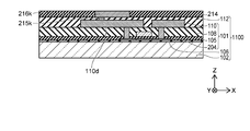
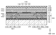
- 3A to 8B are schematic cross-sectional views illustrating the method of manufacturing the image display device of the present embodiment.
- at least one semiconductor growth substrate is prepared.
- a plurality of semiconductor growth substrates (second substrates) 1194-1 and 1194-2 are prepared.
- Each of the semiconductor growth substrates 1194-1 and 1194-2 has a semiconductor layer 1150 formed on the crystal growth substrate (first substrate) 1001.
- the crystal growth substrate 1001 is, for example, a Si substrate, a sapphire substrate, or the like.
- a Si substrate is used.
- the semiconductor layer 1150 includes an n-type semiconductor layer 1151, a light emitting layer 1152, and a p-type semiconductor layer 1153.
- the n-type semiconductor layer 1151, the light emitting layer 1152, and the p-type semiconductor layer 1153 are laminated in the order of the n-type semiconductor layer 1151, the light emitting layer 1152, and the p-type semiconductor layer 1153 from the crystal growth substrate 1001 side.
- a vapor phase growth method (Chemical Vapor Deposition, CVD method) is used, and an organic metal vapor deposition method (Metal Organic Chemical Vapor Deposition, MOCVD method) is preferably used.
- the semiconductor layer 1150 is, for example, In X Al Y Ga 1-XY N (0 ⁇ X, 0 ⁇ Y, X + Y ⁇ 1) or the like.
- crystal defects may occur due to inconsistency of crystal lattice constants, and crystals with crystal defects exhibit n-type. Therefore, when the n-type semiconductor layer 1151 is laminated on the crystal growth substrate 1001 as in this example, a large margin in the production process can be obtained, so that there is an advantage that the yield can be easily improved.
- a metal layer (second metal layer) 1130 is formed on each of the semiconductor growth substrates 1194-1 and 1194-2 on which the semiconductor layer 1150 is formed.
- the metal layer 1130 is formed on the p-type semiconductor layer 1153.
- the surface of the p-type semiconductor layer 1153 on which the metal layer 1130 is formed is a surface facing the surface on which the light emitting layer 1152 is provided.
- the conductive layer 1170 is formed on the p-type semiconductor layer 1153 before the metal layer 1130 is formed.
- the conductive layer 1170 is formed between the metal layer 1130 and the p-type semiconductor layer 1153.
- the conductive layer 1170 is a layer of a conductive layer or a conductive thin film having hole injection properties such as an ITO film.
- the circuit board 1100 is prepared.
- the circuit board (third board) 1100 includes the circuit 101 described with reference to FIG. 1 and the like.
- Contact holes h1 and h2 are formed at positions corresponding to the wirings 110d1 and 110d2 on the first interlayer insulating film 112 of the circuit board 1100, respectively.
- the contact holes h1 and h2 have a depth of reaching the wirings 110d1 and 110d2.
- the depth of the contact holes h1 and h2 may be further formed by over-etching the wirings 110d1 and 110d2.
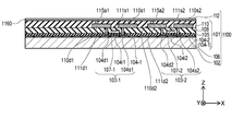
- a metal layer (first metal layer) 1160 is formed on the first interlayer insulating film 112. At the time of forming the metal layer 1160, the materials forming the metal layer 1160 are embedded in the contact holes h1 and h2, and the connecting portions 115a1 and 115a2 are formed.
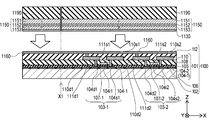
- the semiconductor growth substrates 1194-1 and 1194-2 are inverted upside down and bonded to the circuit board 1100 on which the metal layer 1160 is formed. More specifically, the bonded surfaces of the semiconductor growth substrates 1194-1 and 1194-2 are exposed surfaces of the metal layer 1130. The bonded surface of the circuit board 1100 is an exposed surface of the metal layer 1160. With these faces facing each other, the two are pasted together.
- a plurality of semiconductor growth boards 1194-1 and 1194-2 are attached to one circuit board 1100.
- the position X1 is a position where the respective ends are arranged when the semiconductor growth substrates 1194-1 and 1194-2 are arranged adjacent to each other.
- the light emitting elements 150-1 and 150-2 are not formed in a predetermined region including the position X1.
- each substrate is heated and thermocompression bonded to bond the substrates together.
- a low melting point metal or a low melting point alloy may be used for heat crimping.
- the low melting point metal is, for example, Sn, In, or the like, and the low melting point alloy can be, for example, an alloy containing Zn, In, Ga, Sn, Bi, or the like as a main component.
- the bonded surfaces of each substrate are flattened by chemical mechanical polishing (CMP), etc., and then the bonded surfaces are cleaned and adhered in vacuum by plasma treatment. You may let it.
- CMP chemical mechanical polishing
- FIGS. 5A to 6B show two types of modifications relating to the wafer bonding process.
- the steps of FIGS. 5A to 5C can be used instead of the steps of FIGS. 3A and 4B.
- the steps of FIGS. 6A and 6B may be used.
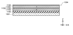
- FIGS. 5A to 5C after the semiconductor layer 1150 is formed on the crystal growth substrate 1001, the semiconductor layer 1150 is transferred to a support substrate 1190 different from the crystal growth substrate 1001. As shown in FIG. 5A, semiconductor growth substrates 1294-1 and 1294-2 are prepared.
- the semiconductor growth substrates 1294-1 and 1294-2 include a semiconductor layer 1150, respectively.
- the semiconductor layer 1150 includes a p-type semiconductor layer 1153, a light emitting layer 1152, and an n-type semiconductor layer 1151.
- the p-type semiconductor layer 1153, the light emitting layer 1152 and the n-type semiconductor layer 1151 are formed on the crystal growth substrate 1001 from the side of the crystal growth substrate 1001 by the p-type semiconductor layer 1153, the light emitting layer 1152 and the n-type semiconductor layer 1151. They are stacked in order.
- the support substrate 1190 is adhered to the exposed surface of the n-type semiconductor layer 1151.
- the support substrate 1190 is made of, for example, Si or quartz.
- the crystal growth substrate 1001 is removed. For removing the crystal growth substrate 1001, for example, wet etching or laser lift-off is used.
- a metal layer 1130 is formed on the exposed surface of the p-type semiconductor layer 1153.
- the circuit board 1100 on which the metal layer 1160 is formed is prepared.
- the metal layer 1130 is arranged so as to face the metal layer 1160, and the metal layers 1130 and 1160 are bonded to each other. After that, the support substrate 1190 is removed by laser lift-off or the like.
- the semiconductor layer 1150 is formed on the buffer layer 1140.
- semiconductor growth substrates 1194a-1 and 1194a-2 are prepared.
- the semiconductor growth substrates 1194a-1 and 1194a-2 include a buffer layer 1140 and a semiconductor layer 1150, respectively.
- the buffer layer 1140 is formed on one surface of the crystal growth substrate 1001.
- the semiconductor layer 1150 is formed on the crystal growth substrate 1001 via the buffer layer 1140.
- nitride such as AlN is preferably used.
- the semiconductor layer 1150 includes an n-type semiconductor layer 1151, a light emitting layer 1152, and a p-type semiconductor layer 1153.
- the n-type semiconductor layer 1151, the light emitting layer 1152, and the p-type semiconductor layer 1153 are placed on the crystal growth substrate 1001 in the order of the n-type semiconductor layer 1151, the light emitting layer 1152, and the p-type semiconductor layer 1153 from the crystal growth substrate 1001 side. Stacked.
- a metal layer 1130 is formed on the exposed surface of the p-type semiconductor layer 1153 on the prepared semiconductor growth substrates 1194a-1 and 1194a-2. As described in FIG. 3A, the conductive layer 1170 is formed between the metal layer 1130 and the p-type semiconductor layer 1153.
- the circuit board 1100 on which the metal layer 1160 is formed is prepared.
- the exposed surface of the metal layer 1130 is arranged so as to face the exposed surface of the metal layer 1160, and the metal layers 1130 and 1160 are bonded to each other.
- the buffer layer 1140 since the buffer layer 1140 remains on the n-type semiconductor layer 1151 after the crystal growth substrate 1001 is removed, the buffer layer 1140 is removed in any of the subsequent steps.
- the step of removing the buffer layer 1140 may be performed, for example, after the step of forming the light emitting element, or may be performed before forming the light emitting element.
- wet etching or the like is used for removing the buffer layer 1140.
- the crystal growth substrate 1001 is removed by wet etching, laser lift-off, or the like.
- the joined metal layers 1130 and 1160 form a metal layer 1160a.
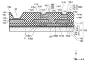
- the semiconductor layer 1150 shown in FIG. 7A is formed into a desired shape by etching to form light emitting elements 150-1 and 150-2.
- a dry etching process is used, and preferably anisotropic plasma etching (Reactive Ion Etching, RIE) is used.
- RIE reactive Ion Etching
- the joined metal layer 1160a shown in FIG. 7A is etched to form a wiring layer (third wiring layer) 116.
- the wiring layer 116 includes plugs 116a1, 116a2 and wiring 116k.
- the conductive thin film 117a1 covers the plug 116a1, and the conductive thin film 117a2 covers the plug 116a2.
- the conductive thin film 117k covers the wiring 116k.
- the outer circumference of the plug 116a1 is formed so as to include the outer circumference of the light emitting element 150-1 projected on the plug 116a1 in an XY plan view.
- the outer circumference of the plug 116a2 is formed so as to include the outer circumference of the light emitting element 150-2 projected on the plug 116a2 in an XY plan view.
- the light emitting elements 150-1 and 150-2 are formed at positions sufficiently distant from the position X1.
- the position X1 is a position corresponding to the end portion of the semiconductor layer 1150 shown in FIG. 4B, and the crystal quality of the semiconductor layer 1150 is likely to deteriorate at or near the position corresponding to the position X1. Therefore, the light emitting elements 150-1 and 150-2 are formed at positions sufficiently separated from the end portions on the positive direction side of the X-axis from the position X1. On the negative direction side of the X-axis from the position X1, in this example, no other circuit element including the light emitting element is formed, and the wiring 116k is formed.
- the second interlayer insulating film 156 is formed by covering the first interlayer insulating film 112, the plugs 116a1, 116a2, the wiring 116k, the conductive thin films 117a1, 117a2, 117k and the light emitting elements 150-1, 150-2.
- a part of the second interlayer insulating film 156 is removed by etching until it reaches the n-type semiconductor layer 151-1 to form an opening 158-1.
- a part of the second interlayer insulating film 156 to be removed is a position corresponding to the light emitting element 150-1.
- the light emitting surface 151S1 is exposed from the second interlayer insulating film 156.
- a part of the second interlayer insulating film 156 is removed by etching until it reaches the n-type semiconductor layer 151-2 to form an opening 158-2.
- a part of the second interlayer insulating film 156 to be removed is a position corresponding to the light emitting element 150-2.
- the light emitting surface 151S2 is exposed from the second interlayer insulating film 156.
- a part of the second interlayer insulating film 156 is removed by etching until it reaches the conductive thin film 117k to form an opening 162.
- a part of the second interlayer insulating film 156 to be removed is a position corresponding to the wiring 116k.
- the conductive thin film 117k is exposed from the second interlayer insulating film 156.
- the openings 158-1, 158-2, 162 are formed, for example, at the same time.
- the surface of the second interlayer insulating film 156 has a flatness enough to cover the light emitting elements 150-1 and 150-2. Just do it.
- the light emitting surface 151S1 of the exposed n-type semiconductor layer 151-1 and the light emitting surface 151S2 of the n-type semiconductor layer 151-2 are roughened in order to improve the luminous efficiency.
- a second wiring layer 159 is formed on the second interlayer insulating film 156.
- the second wiring layer 159 includes a translucent electrode 159k.
- the translucent electrode 159k is formed over the surface of the conductive thin film 117k exposed from the second interlayer insulating film 156 by the opening 162 and the light emitting surfaces 151S1 and 151S2.
- the translucent electrode 159k electrically connects the n-type semiconductor layers 151-1, 151-2 to the conductive thin film 117k and the wiring 116k.
- the metal layers 1130 and 1160 are formed on both the semiconductor growth boards 1194-1 and 1194-2 and the circuit board 1100, but at least if the metal layer 1160 is provided on the circuit board 1100 side. Good.
- a part of the circuit other than the subpixels 20-1 and 20-2 is formed in the circuit board 1100.
- the row selection circuit 5 shown in FIG. 2 is formed in the circuit board 1100 together with the drive transistor, the selection transistor, and the like. That is, the row selection circuit 5 may be incorporated at the same time by the manufacturing process described above.
- the signal voltage output circuit 7 is incorporated in a semiconductor device manufactured by a manufacturing process capable of high integration by microfabrication.
- the signal voltage output circuit 7 is mounted on another board together with the CPU and other circuit elements, and is interconnected with the wiring of the circuit board 1100, for example, before incorporating the color filter described later or after incorporating the color filter. Will be done.
- the circuit board 1100 includes a substrate 102 made of a glass substrate including the circuit 101, and the substrate 102 is, for example, substantially square. As described above, the circuit board 1100 is formed with a circuit 101 for one image display device 1. Alternatively, the circuit board 1100 may be formed with circuits 101 for a plurality of image display devices. In the case of a larger screen size or the like, the circuit 101 for forming one image display device is divided into a plurality of circuit boards 1100 and formed, and all the divided circuits are combined to form one image. A display device may be configured.
- a semiconductor layer 1150 having substantially the same dimensions as the crystal growth substrate 1001 is formed on the crystal growth substrate 1001.
- the crystal growth substrate 1001 can be a square having the same dimensions as the square circuit board 1100.
- the crystal growth substrate is not limited to the same shape as the circuit board 1100 or a similar shape, and may have other shapes.
- the crystal growth substrate 1001 may have a substantially circular wafer shape or the like having a diameter including the circuit 101 formed on the square circuit board 1100.
- FIG. 9 is a perspective view illustrating a method of manufacturing the image display device of the present embodiment.
- a plurality of semiconductor growth substrates 1194-1, 1194-2, 1194-3, etc. are prepared, and semiconductor layers formed on one circuit board 1100 and a plurality of crystal growth substrates 1001.
- the 1150 may be joined.
- the semiconductor growth substrate 1194-3 is the same as the semiconductor growth substrates 1194-1, 1194-2 described above, and the semiconductor growth substrates 1194-1, 1194-2, 1194-3, etc. are shown in FIG. 3A and the like.
- a semiconductor layer 1150 is formed on the crystal growth substrate 1001.
- a plurality of circuits 101 are arranged, for example, in a grid pattern on one board 102.
- the circuit 101 includes all the subpixels 20-1, 20-2, etc. required for one image display device 1.
- the circuits 101 arranged adjacent to each other are provided with an interval of about the width of the scribe line. No circuit element or the like is arranged at the end of the circuit 101 or near the end.
- the semiconductor layer 1150 is formed so that its end portion coincides with the end portion of the crystal growth substrate 1001. Therefore, the ends of the semiconductor growth substrates 1194-1, 1194-2, and 1194-3 are arranged so as to coincide with the ends of the circuit 101 and joined to form a circuit with the ends of the semiconductor layer 1150 after joining. It can be matched with the end of 101.
- the crystal quality is likely to deteriorate at the end of the semiconductor layer 1150 and its vicinity. Therefore, by matching the end of the semiconductor layer 1150 with the end of the circuit 101, the crystal quality in the vicinity of the end of the semiconductor layer 1150 on the semiconductor growth substrates 1194-1, 1194-2, 1194-3 is deteriorated. It is possible to prevent the easy area from being used as the display area of the image display device 1.
- the boundary between the two adjacent semiconductor layers 1150 and the vicinity of the boundary are used. It is preferable to arrange the circuit so as not to form the light emitting elements 150-1 and 150-2 in the region.
- a plurality of circuit boards 1100 may be prepared and the plurality of circuit boards 1100 may be bonded to the semiconductor layer 1150 formed on one semiconductor growth substrate.
- FIG. 10 is a schematic cross-sectional view illustrating the method for manufacturing the image display device of the present embodiment.
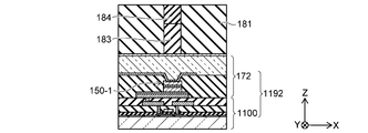
- the structure inside the circuit board 1100, the first interlayer insulating film 112, the connecting portions 115a1, 115a2, the plugs 116a1, 116a2, the wiring 116k, the conductive thin films 117a1, 117a2, 117k, and the first The display of the wiring layer 159 and the like of No. 2 is omitted. Further, in FIG. 10, a part of the color conversion member such as the color filter 180 is displayed. In FIG.
- a structure including light emitting elements 150-1, 150-2, a second interlayer insulating film 156, a surface resin layer 170, a plug whose display is omitted, and the like is referred to as a light emitting circuit unit 172. Further, a structure in which the light emitting circuit unit 172 is provided on the circuit board 1100 is referred to as a structure 1192.
- the color filter (wavelength conversion member) 180 is adhered to the structure 1192 on one surface.
- the other surface of the color filter 180 is adhered to the glass substrate 186.
- a transparent thin film adhesive layer 188 is provided on one surface of the color filter 180, and is adhered to the surface of the structure 1192 on the light emitting circuit portion 172 side via the transparent thin film adhesive layer 188.
- the color filter 180 has color conversion units arranged in the positive direction of the X-axis in the order of red, green, and blue.
- a red color conversion layer 183R is provided on the first layer
- a green color conversion layer 183G is provided on the first layer
- a filter layer 184 is provided on the second layer.
- Each is provided.
- a single-layer color conversion layer 183B may be provided, or a filter layer 184 may be provided.
- a light-shielding unit 181 is provided between the color conversion units, but it goes without saying that the frequency characteristics of the filter layer 184 can be changed for each color of the color conversion unit.
- the color filter 180 is attached to the structure 1192 by aligning the positions of the color conversion layers 183R, 183G, and 183B of each color with the positions of the light emitting element 150.
- 11A to 11D are schematic cross-sectional views showing a modified example of the manufacturing method of the image display device of the present embodiment.
- 11A-11D show a method of forming a color filter by inkjet.
- a structure 1192 in which the light emitting circuit unit 172 is attached to the circuit board 1100 is prepared.
- a light-shielding portion 181 is formed on the structure 1192.
- the light-shielding portion 181 is formed by using, for example, screen printing, photolithography technology, or the like.
- the phosphor corresponding to the emitted color is ejected from the inkjet nozzle to form the color conversion layer 183.
- the phosphor colors the region where the light-shielding portion 181 is not formed.
- a fluorescent paint using a general phosphor material, a perovskite phosphor material, or a quantum dot phosphor material is used.
- a perovskite phosphor material or a quantum dot phosphor material it is preferable because each emission color can be realized, the monochromaticity is high, and the color reproducibility can be high.
- the drying process is performed at an appropriate temperature and time. The thickness of the coating film at the time of coloring is set to be thinner than the thickness of the light-shielding portion 181.
- the color conversion layer 183 is not formed for the blue light emitting subpixel if the color conversion unit is not formed. Further, when the blue color conversion layer is formed for the blue light emitting subpixel, if the color conversion unit may be one layer, the thickness of the coating film of the blue phosphor is preferably the light-shielding portion 181. It is said to be about the same thickness as.
- the paint for the filter layer 184 is ejected from the inkjet nozzle.
- the paint is applied over the coating film of the phosphor.
- the total thickness of the coating film of the phosphor and the paint is about the same as the thickness of the light-shielding portion 181.
- the semiconductor layer 1150 is bonded to the circuit board 1100 including the circuit elements such as the transistors 103-1 and 103-2 for driving the light emitting elements 150-1 and 150-2. .. Then, the semiconductor layer 1150 is etched to form the light emitting elements 150-1 and 150-2. Therefore, the step of transferring the light emitting element can be remarkably shortened as compared with the case of individually transferring the light emitting element separated into the circuit board 1100.
- the number of subpixels exceeds 24 million, and in the case of an 8K image quality image display device, the number of subpixels exceeds 99 million. It takes an enormous amount of time to mount such a large number of light emitting elements individually on a circuit board, and it is difficult to realize an image display device using micro LEDs at a realistic cost. Further, if a large number of light emitting elements are individually mounted, the yield is reduced due to poor connection at the time of mounting, and further cost increase is unavoidable.
- the entire semiconductor layer 1150 is attached to the circuit board 1100 before the semiconductor layer 1150 is fragmented, so that the transfer step is completed in one time.
- the semiconductor layer 1150 is attached to the circuit board 1100 at the wafer level without being fragmented in advance or forming electrodes at positions corresponding to the circuit elements, there is no need to perform alignment. Therefore, the pasting process can be easily performed in a short time. Since it is not necessary to align the light emitting element 150 at the time of pasting, the light emitting element 150 can be easily miniaturized, which is suitable for a high-definition display.
- the TFT formed on the glass substrate can be used as the circuit board 1100, so that the existing flat panel manufacturing process or plant can be used.
- the plugs 116a1 and 116a2 are formed on the circuit board 1100.
- the plug 116a1 is electrically connected to the driving transistor 103-1.
- the plug 116a2 is electrically connected to the driving transistor 103-2.
- the light emitting elements 150-1 and 150-2 are formed on the plugs 116a1 and 116a2, respectively. Therefore, the light emitting element 150-1 is surely electrically connected to the transistor 103-1 and the light emitting element 150-2 is surely electrically connected to the transistor 103-2. Therefore, the decrease in yield due to poor connection of the light emitting element or the like is suppressed.
- the wiring layer 116 having the wiring 116k is formed on the same layer as the plugs 116a1 and 116a2. Since the wiring 116k is formed on the same circuit board 1100 as the plugs 116a1 and 116a2, the wiring 116k can be used as wiring that requires low impedance such as a power supply line and a ground line, and the wiring and arrangement of the circuit 101 can be arranged. The degree of layout freedom can be increased. Since the wiring 116k is formed at the same time as the plugs 116a1 and 116a2, low impedance wiring can be easily realized without adding a step for the wiring 116k.
- the electrical connection on the light emitting surfaces 151S1 and 151S2 sides is made via the translucent electrode 159k. Therefore, a sufficient area of the light emitting surfaces 151S1 and 151S2 can be secured, and high luminous efficiency can be realized.
- the plugs 116a1 and 116a2 also function as light reflection plates.
- the light scattered downward from the light emitting elements 150-1 and 150-2 is reflected by the plugs 116a1 and 116a2 and distributed to the light emitting surfaces 151S1 and 151S2. Therefore, the luminous efficiency of the light emitting elements 150-1 and 150-2 is substantially improved.
- the plugs 116a1 and 116a2 function as a light reflecting plate and also as a light shielding plate.
- the plugs 116a1 and 116a2 block the light scattered downward from the light emitting elements 150-1 and 150-2. Therefore, it is possible to suppress the irradiation of light to the circuit elements in the vicinity of the light emitting elements 150-1 and 150-2, and prevent the circuit elements from malfunctioning.
- the wiring 116k or the first wiring layer 110 for wiring such as the power supply line and the ground line
- the degree of freedom of the wiring pattern of the power supply line and the ground line is improved, and the design efficiency of the image display device is improved. Can be improved.
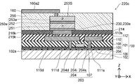
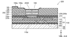
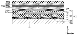
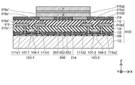
- FIG. 12 is a schematic cross-sectional view illustrating a part of the image display device according to the present embodiment.
- FIG. 12 schematically shows a cross section when the subpixel 220 is cut along a plane parallel to the XZ plane.
- This embodiment differs from the other embodiments described above in that the flattening film 214 is included and the plug 216k is embedded in the flattening film 214.
- one subpixel 220 will be described, but as in the case of the other embodiments, a plurality of subpixels 220 are provided on the XY plane and are arranged in the X-axis direction and the Y-axis direction. ing.
- the area of the light emitting element 250 may be different depending on the light emitting color and the like.
- the same components as in the case of the other embodiments described above are designated by the same reference numerals, and detailed description thereof will be omitted as appropriate.
- the subpixel 220 of the image display device of the present embodiment includes a transistor 203, a first wiring layer 110, a first interlayer insulating film 112, a plug 216k, a light emitting element 250, and the like. It includes a second interlayer insulating film 156 and a second wiring layer 160. Subpixel 220 further includes a color filter 180, as in the other embodiments described above.
- Transistor 203 is formed on the substrate 102.
- Transistor 203 is an n-channel TFT in this example.
- Transistor 203 includes a TFT channel 204 and a gate 107.
- the transistor 203 is formed by an LTPS process or the like, as in the other embodiments described above.
- the circuit 101 includes a TFT channel 204, an insulating layer 105, an insulating film 108, vias 111s and 111d, and a first wiring layer 110.
- the TFT channel 204 includes regions 204s, 204i, 204d. Regions 204s, 204i, 204d are provided on the TFT underlayer film 106. Regions 204s and 204d are doped with n-type impurities such as P (phosphorus). The region 204s is ohmic contacted with the via 111s. Region 204d is ohmic contacted with via 111d.
- the gate 107 is provided on the TFT channel 204 via the insulating layer 105.
- the insulating layer 105 insulates the TFT channel 204 and the gate 107.
- the transistor 203 when a voltage higher than the region 204s is applied to the gate 107, a channel is formed in the region 204i.
- the current flowing between the regions 204s and 204d is controlled by the voltage of the gate 107 with respect to the region 204s.
- the TFT channel 204 and the gate 107 are formed of the same materials and manufacturing methods as the TFT channels 104-1 and 104-2 and the gates 107-1 and 107-2 in the case of the other embodiments described above.
- the vias 111s and 111d are provided so as to penetrate the insulating film 108.
- the via 111s is provided between the wiring 110s and the area 204s.
- the via 111s electrically connects the wiring 110s and the area 204s.
- the via 111d is provided between the wiring 110d and the area 204d.
- the via 111d electrically connects the wiring 110d and the area 204d.
- the vias 111s and 111d are formed of the same materials and manufacturing methods as the vias 111s1, 111d1 and the like in the case of the other embodiments described above.
- the wiring 110s is electrically connected to, for example, the ground wire 4 of the circuit shown in FIG. 15 described later.
- the wiring 110d is electrically connected to the n-type semiconductor layer 251 via a connecting portion 215k, a plug 216k, and a light reflecting plate 230a.
- the flattening film 214 is provided on the first interlayer insulating film 112.
- the flattening film 214 is a film or layer having an insulating property, and like the first interlayer insulating film 112, for example, an organic insulating film such as PSG or BPSG, an inorganic insulating film such as SOG (Spin On Glass), or the like. is there.
- the plug 216k is provided on the first interlayer insulating film 112.
- the side surface of the plug 216k is covered with a flattening film 214. That is, the plug 216k is embedded in the flattening film 214.
- the plug 216k and the flattening film 214 each have the same plane substantially parallel to the XY plane.
- the surfaces of the plug 216k and the flattening film 214 are collectively flattened surfaces as will be described later.
- a connection portion 215k is provided between the plug 216k and the wiring 110d.
- the connecting portion 215k is formed of a conductive member, and electrically connects the plug 216k and the wiring 110d.
- the plug 216k and the connection portion 215k are made of, for example, the same material as the first wiring layer 110.
- the light emitting element 250 is provided on the plug 216k via the light reflection plate 230a.
- the light emitting element 250 includes an n-type semiconductor layer (first semiconductor layer) 251 and a light emitting layer 252, and a p-type semiconductor layer (second semiconductor layer) 253.
- the n-type semiconductor layer 251 and the light emitting layer 252 and the p-type semiconductor layer 253 are formed by the n-type semiconductor layer 251 and the light emitting layer 252 and the p-type semiconductor layer from the side of the first interlayer insulating film 112 toward the light emitting surface 253S. They are stacked in the order of 253. Therefore, the n-type semiconductor layer 251 is electrically connected to the plug 216k via the light reflecting plate 230a.
- the light emitting element 250 has the same XY plan view shape as the light emitting elements 150-1 and 150-2 of the other embodiments described above. An appropriate shape is selected according to the layout of the circuit element and the like.
- the light emitting element 250 is a light emitting diode similar to the light emitting elements 150-1 and 150-2 of the other embodiments described above. That is, the wavelength of the light emitted by the light emitting element 250 is, for example, blue light emission of about 467 nm ⁇ 20 nm or blue-purple light emission of about 410 nm ⁇ 20 nm.
- the wavelength of the light emitted by the light emitting element 250 is not limited to the above-mentioned value, and may be appropriate.
- the second wiring layer (second wiring layer) 160 is provided on the second interlayer insulating film 156.
- the second wiring layer 160 includes the wiring 160a.
- the wiring 160a is connected to, for example, the power supply line 3 of the circuit shown in FIG. 15 described later.
- the second wiring layer 160 is made of the same material as, for example, the first wiring layer 110.
- the third wiring layer 230 is provided on the flattening film 214 and the plug 216k.
- the third wiring layer 230 includes a light reflecting plate 230a.
- the light reflecting plate 230a is provided for each subpixel, and the plurality of light reflecting plates 230a are electrically insulated.
- the light emitting elements 250 are provided on the light reflecting plate 230a, respectively.
- the third wiring layer 230 and the light reflection plate 230a are made of a material having high conductivity.
- the light reflecting plate 230a contains, for example, Ti, Al, an alloy of Ti and Sn, and the like. It may contain a noble metal having high light reflectivity such as Cu and V, or Ag and Pt. Since the light reflecting plate 230a is made of such a metal material having high conductivity or the like, the light emitting element 250 and the circuit 101 are electrically connected with low resistance.
- the outer circumference of the light reflecting plate 230a includes the outer circumference when the light emitting element 250 is projected onto the light reflecting plate 230a in XY plan view.
- the fact that the outer circumference of the light reflecting plate 230a includes the outer circumference of the light emitting element 250 also includes that the outer circumferences of the light reflecting plate 230a are the same.
- the light reflecting plate 230a can reflect the scattered light downward of the light emitting element 250 toward the light emitting surface 253S.
- the luminous efficiency of the light emitting element 250 can be substantially improved.
- the translucent electrode 159a is provided over the wiring 160a.
- the translucent electrode 159a is provided over the light emitting surface 253S of the opened p-type semiconductor layer 253.
- the translucent electrode 159a is provided between the wiring 160a and the light emitting surface 253S, and electrically connects the wiring 160a and the p-type semiconductor layer 253.
- the n-type semiconductor layer 251 is electrically connected to the region 204d via the light reflecting plate 230a, the plug 216k, the connecting portion 215k, the wiring 110d, and the via 111d.
- Region 204d corresponds to the drain electrode of transistor 203.
- the region 204s corresponds to the source electrode of the transistor 203 and is electrically connected to the ground wire 4 via the via 111s and the wiring 110s.
- the p-type semiconductor layer 253 is electrically connected to the power supply line 3 via the translucent electrode 159a and the wiring 160a.
- FIG. 13 is a schematic cross-sectional view illustrating a part of a modified example of the image display device of the present embodiment. As shown in FIG. 13, in the sub-pixel 220a of this modification, the plug 216k is connected to the wiring 110d without going through the connection portion 215k shown in FIG.
- the plug 216k when the plug 216k is connected to the wiring 110d via the connection portion 215k, the outer circumference of the plug 216k protrudes outside the outer circumference of the wiring 110d in the XY plan view. It is possible to.
- the plug 216k is provided directly on the wiring 110d without the connection portion 215k as in this modification. be able to. That is, depending on the positional relationship between the plug and the connection destination wiring and the shape of each of the plug and the connection destination wiring, the wiring and the element are connected to each other with or without a connection portion. be able to. This also applies to each embodiment and modification described below.
- FIGS. 14A and 14B are schematic cross-sectional views illustrating a part of a modification of the image display device of the present embodiment.
- the display of the surface resin layer 170, the transparent thin film adhesive layer 188, and the color filter 180 is omitted in order to avoid complication.
- a surface resin layer 170, a transparent thin film adhesive layer 188, and a color filter 180 are provided on the second interlayer insulating film and the second wiring layer. The same applies to the other embodiments described later and the modified examples thereof.
- the structure of the wiring for electrical connection on the light emitting surface 253S side is different from that of the second embodiment.
- the other components are the same as in the second embodiment, and the same components are designated by the same reference numerals and detailed description thereof will be omitted as appropriate.
- the subpixel 220b includes a second wiring layer 160, and the second wiring layer 160 includes wiring 160a1.
- the wiring 160a1 is provided on the second interlayer insulating film 156.
- the wiring 160a1 is electrically connected to the p-type semiconductor layer 253 by connecting one end of the wiring 160a1 to the surface including the light emitting surface 253S.
- the surface connecting one end of the wiring 160a1 is a surface coplanar with the light emitting surface 253S.
- the step of forming the translucent electrode can be omitted.
- the light emitting surface 253S is preferably roughened as in this example.
- the configuration of the second interlayer insulating film 256 and the wiring 160a2 is different from that of the second embodiment.
- the subpixel 220c includes a second interlayer insulating film 256.
- the second wiring layer 160 includes the wiring 160a2, and the wiring 160a2 is provided on the second interlayer insulating film 256.
- the second interlayer insulating film 256 is a transparent resin.
- the second interlayer insulating film 256 is not provided with an opening corresponding to the position of the light emitting surface 253S.
- the wiring 160a2 of the second wiring layer 160 is directly connected to the light emitting surface 253S.
- the light emitting element 250a emits light from the light emitting surface 253S via the second interlayer insulating film 256.
- the step of forming an opening in the second interlayer insulating film 256 and roughening the p-type semiconductor layer 253a can be omitted.
- the second interlayer insulating film 256 is formed of, for example, a transparent organic insulating material.
- a transparent resin material a silicon-based resin such as SOG (Spin On Glass), a novolak-type phenol-based resin, or the like is used. Similar to the other embodiments described above, the second interlayer insulating film 256 is insulation between light emitting elements and is provided for protection from the external environment.
- the surface of the second interlayer insulating film 256 may be as flat as the second interlayer insulating film 156 so that the second wiring layer 160 can be formed.
- the configuration including the surface resin layer 170, the transparent thin film adhesive layer 188, and the color filter 180 is provided as in the case of the other embodiments described above.
- FIG. 15 is a schematic block diagram illustrating an image display device according to the present embodiment.
- the image display device 201 of the present embodiment includes a display area 2, a row selection circuit 205, and a signal voltage output circuit 207.
- the sub-pixels 220 are arranged in a grid pattern on the XY plane, as in the case of the other embodiments described above.
- Pixel 10 includes a plurality of subpixels 220 that emit light of different colors, as in the case of the other embodiments described above.
- the subpixel 220R emits red light.
- the subpixel 220G emits green light.
- the subpixel 220B emits blue light.
- the emission color and brightness of one pixel 10 are determined by the three types of sub-pixels 220R, 220G, and 220B emitting light with desired brightness.
- One pixel 10 is composed of three sub-pixels 220R, 220G, 220B, and the sub-pixels 220R, 220G, 220B are linearly arranged on the X-axis, for example, as in this example.
- Each pixel 10 may have sub-pixels of the same color arranged in the same column, or sub-pixels of different colors may be arranged in each column as in this example.
- the subpixel 220 includes a light emitting element 222, a selection transistor 224, a drive transistor 226, and a capacitor 228.
- the selection transistor 224 may be displayed as T1
- the drive transistor 226 may be displayed as T2
- the capacitor 228 may be displayed as Cm.
- the light emitting element 222 is provided on the power supply line 3 side, and the drive transistor 226 connected in series with the light emitting element 222 is provided on the ground line 4 side. That is, the drive transistor 226 is connected to the lower potential side than the light emitting element 222.
- the drive transistor 226 is an n-channel transistor.
- a selection transistor 224 is connected between the gate electrode of the drive transistor 226 and the signal line 208.
- the capacitor 228 is connected between the gate electrode of the drive transistor 226 and the ground wire 4.
- the row selection circuit 205 and the signal voltage output circuit 207 supply a signal voltage having a polarity different from that of the other embodiment described above to the signal line 208 in order to drive the drive transistor 226 which is an n-channel transistor.
- the row selection circuit 205 supplies a selection signal to the scanning line 206 so as to sequentially select one row from the array of subpixels 220 in the m row.
- the signal voltage output circuit 207 supplies a signal voltage having the required analog voltage value to each subpixel 220 in the selected row.
- the drive transistor 226 of the subpixel 220 in the selected row causes a current corresponding to the signal voltage to flow through the light emitting element 222.
- the light emitting element 222 emits light with a brightness corresponding to the flowing current.
- any of the configurations of the subpixels 220, 220a, 220b, and 220c shown above can be included.
- the modification of the subpixel can be applied to each of the embodiments described below.
- 16A to 20C are schematic cross-sectional views illustrating the method of manufacturing the image display device of the present embodiment.
- 16A-18B show a procedure for forming a plug on the circuit board 1100.
- a plug forming method different from the plug forming method described in the first embodiment is adopted.
- the circuit board 1100 is prepared.
- the circuit board 1100 to be prepared may be the same as in the case of the first embodiment.
- the contact hole h is formed in the first interlayer insulating film 112.
- the position where the contact hole h is formed is a position corresponding to the wiring 110d.
- the contact hole h is formed deeper than the depth of reaching the wiring 110d from the first interlayer insulating film 112.
- the depth of the contact hole h may be up to the surface of the wiring 110d if a sufficient exposed area of the wiring 110d can be secured.
- the metal layer 1116 is formed over the first interlayer insulating film 112.
- the contact hole h shown in FIG. 16B is embedded with the same material as the metal layer 1116.
- a connecting portion 215k is formed in the embedded portion.
- the plug 216k is formed into a desired shape from the metal layer 1116 shown in FIG. 17A by photolithography, dry etching, or the like.
- the flattening film 1114 is applied so as to cover the first interlayer insulating film 112 and the plug 216k, and then fired.
- the surface of the flattening film 1114 shown in FIG. 18A is polished so that the surface of the plug 216k is exposed.
- the plug 216k and the flattening film 214 are collectively polished and flattened.
- CMP is used for polishing the flattening film 1114. In this way, the plug 216k, the connecting portion 215k and the flattening film 214 are formed.
- the first interlayer insulating film 112 is etched according to the shape of the plug 216k until it reaches at least the surface of the wiring 110d. To do. Then, as shown in FIGS. 17A and 17B, after forming the metal layer 1116, the metal layer 1116 is formed into a desired plug 216k shape. As shown in FIGS. 18A and 18B, after the flattening film 1114 is formed, the flattening film 1114 can be collectively flattened by CMP or the like to form the plug 216k and the flattening film 214.
- the semiconductor growth substrate 1294 is prepared.
- the semiconductor growth substrate 1294 includes a crystal growth substrate 1001, a buffer layer 1140, and a semiconductor layer 1150.
- the buffer layer 1140 is formed on the crystal growth substrate 1001.
- the semiconductor layer 1150 is formed on the buffer layer 1140.
- the semiconductor layer 1150 includes a p-type semiconductor layer 1153, a light emitting layer 1152, and an n-type semiconductor layer 1151.
- the p-type semiconductor layer 1153, the light emitting layer 1152, and the n-type semiconductor layer 1151 are laminated in the order of the p-type semiconductor layer 1153, the light emitting layer 1152, and the n-type semiconductor layer 1151 from the side of the buffer layer 1140.
- the metal layer 1130 is formed on the exposed surface of the n-type semiconductor layer 1151.
- a semiconductor growth substrate 1294 on which the metal layer 1130 is formed and a circuit board (third substrate) 1100 on which the plug 216k is formed are prepared.
- the surface on which the plug 216k and the flattening film 214 of the circuit board 1100 are formed is arranged so as to face the exposed surface of the metal layer 1130 of the semiconductor growth substrate 1294.
- the facing surfaces are joined to each other.
- the bonding between the substrates is the same as in the case of the other embodiments described above.
- a modified example of the manufacturing method described in relation to FIGS. 5A to 5C may be applied.
- the semiconductor growth substrate one in which the semiconductor layer 1150 is directly formed on the crystal growth substrate 1001 without providing the buffer layer 1140 may be used.
- the crystal growth substrate 1001 shown in FIG. 19B is removed by laser lift-off or the like.
- the buffer layer 1140 shown in FIG. 19B is removed by wet etching or the like.
- the buffer layer 1140 may be removed after etching the semiconductor layer 1150.
- the semiconductor layer 1150 and the metal layer 1130 shown in FIG. 20A are formed into a desired shape by RIE or the like.
- a third wiring layer 230 is formed from the metal layer 1130, and the third wiring layer 230 includes a light reflection plate 230a.
- the outer circumference of the light reflecting plate 230a is formed so as to substantially coincide with the outer circumference of the light emitting element 250 projected on the light reflecting plate 230a in the XY plan view.
- the semiconductor layer 1150 When the semiconductor layer 1150 is not over-etched, the semiconductor layer 1150 is etched to form the light emitting element 250, and then the metal layer 1130 is etched to form the third wiring layer 230.
- the outer circumference of the light reflecting plate 230a includes the outer circumference of the light emitting element 250 projected on the light reflecting plate 230a in the XY plan view, and can be made larger than the outer circumference of the light emitting element 250.
- the second interlayer insulating film 156 is formed so as to cover the flattening film 214, the third wiring layer 230, and the light emitting element 250.
- a part of the second interlayer insulating film 156 is removed by etching to form an opening 158, and the light emitting surface 253S is the second interlayer insulating film. Exposed from 156.
- the light emitting surface 253S of the exposed p-type semiconductor layer 253 is roughened in order to improve the luminous efficiency.
- a second wiring layer 160 is formed on the second interlayer insulating film 156.
- each wiring including the wiring 160a is formed by photolithography.
- the wiring 160a is provided at a position separated from the p-type semiconductor layer 253.
- a translucent conductive film covering the second wiring layer 160, the second interlayer insulating film 156, and the light emitting surface 253S is formed.
- the translucent conductive film an ITO film, a ZnO film, or the like is preferably used.
- the desired translucent electrode 159a is formed by photolithography.
- the translucent electrode 159a is formed over the wiring 160a.
- the translucent electrode 159a is formed over the light emitting surface 253S.
- the translucent electrode 159a is formed between the wiring 160a and the light emitting surface 253S. Therefore, the wiring 160a and the p-type semiconductor layer 253 are electrically connected by the translucent electrode 159a.
- 21A to 22B are schematic cross-sectional views illustrating a manufacturing method of a modified example of the image display device of the present embodiment.
- 21A and 21B represent a manufacturing process for forming the subpixel 220b of the modification shown in FIG. 14A.
- 22A and 22B represent a manufacturing process for forming the subpixel 220c of the modification shown in FIG. 14B. Since the steps of FIGS. 21A and 22A are both executed after the steps shown in FIG. 20B, the steps after FIG. 20B will be described in the following description.
- the opening 158 is formed after the second interlayer insulating film 156 is formed so as to cover the flattening film 214, the third wiring layer 230, and the light emitting element 250. It is formed.
- the opening 158 is formed so that the light emitting surface 253S is exposed from the second interlayer insulating film 156 by removing a part of the second interlayer insulating film 156. In this example, the light emitting surface 253S is roughened.
- the second wiring layer 160 is formed.
- the second wiring layer 160 includes wiring 160a1.
- the wiring 160a1 is connected to the surface of the p-type semiconductor layer 253 including the light emitting surface 253S at one end of the wiring 160a1.
- the surface to which one end of the wiring 160a1 is connected is a surface parallel to the light emitting surface 253S.
- the second interlayer insulating film 256 is formed so as to cover the flattening film 214, the third wiring layer 230, and the light emitting element 250.
- the second interlayer insulating film 256 is formed of a transparent resin.
- the second wiring layer 160 is formed after the contact hole is formed in the second interlayer insulating film 256.
- the second wiring layer 160 includes wiring 160a2.
- the wiring 160a2 is connected to the surface of the p-type semiconductor layer 253 including the light emitting surface 253S via the contact hole.
- the sub-pixel 220 of the image display device 201 of the present embodiment and the sub-pixels 220a, 220b, 220c of the modified example are formed.
- the subpixels 220, 220a, 220b, 220c include the light reflection plate 230a in addition to the plug 216k, so that the plug 216k is used. It can be miniaturized.
- FIG. 23 is a schematic cross-sectional view illustrating a part of the image display device according to the present embodiment.
- FIG. 23 schematically shows a cross section when the subpixel 320 is cut along a plane parallel to the XZ plane.
- the light emitting element 150 is different from the case of the second embodiment and the modified example thereof in that the light emitting element 150 is provided on the plug 216a without passing through the light reflecting plate.
- the same components as in the case of the other embodiments described above are designated by the same reference numerals, and detailed description thereof will be omitted as appropriate.
- the subpixel 320 of the image display device of the present embodiment includes a transistor 103, a light emitting element 150, and a plug 216a.
- the transistor 103 is formed on the first surface 102a of the substrate 102, as in the case of the other embodiments described above.
- the transistor 103 includes a TFT channel 104 and a gate 107.
- the TFT channel 104 includes regions 104s, 104i, 104d. Regions 104s, 104i, 104d are provided on the TFT underlayer film 106. The area 104i is provided between the areas 104s and 104d. The regions 104s and 104d are ohmicly connected to the vias 111s and 111d, respectively.
- the transistor is a p-channel TFT.
- the gate 107 is provided on the TFT channel 104 via the insulating layer 105.
- the TFT channel 104 and the gate 107 are insulated from each other by an insulating layer 105.
- Each region 104s, 104i, 104d and gate 107 of the TFT channel 104 are formed by the same material and manufacturing method as in the case of the first embodiment.
- the vias 111s and 111d and the wirings 110s and 110d are configured in the same manner as in the case of the second embodiment and its modifications, and are formed of the same materials and manufacturing methods.
- the light emitting element 150 is provided on the plug 216a.
- the plug 216a is connected to the wiring 110d via the connecting portion 215a.
- the light emitting element 150 includes a p-type semiconductor layer 153, a light emitting layer 152, and an n-type semiconductor layer 151.
- the p-type semiconductor layer 153, the light emitting layer 152, and the n-type semiconductor layer 151 are laminated in the order of the p-type semiconductor layer 153, the light emitting layer 152, and the n-type semiconductor layer 151 from the plug 216a side toward the light emitting surface 151S. ing.
- the p-type semiconductor layer 153 is electrically connected to the region 104d via the plug 216a, the connecting portion 215a, the wiring 110d, and the via 111d.
- the wiring 110s is connected to the power supply line 3 of the circuit shown in FIG.
- the wiring 110s is connected to the region 104s via the via 111s. Therefore, the region 104s is electrically connected to the power supply line 3 via the via 111s and the wiring 110s.
- the outer circumference of the plug 216a is set to include the outer circumference of the light emitting element 150 when the light emitting element 150 is projected onto the plug 216a in an XY plan view.
- the plug 216a functions as a light reflecting plate.
- the plug 216a reflects the light scattered downward of the light emitting element 150 toward the light emitting surface 151S.
- the plug 216a shields the light scattered downward from the light emitting element 150 and suppresses the arrival of the light at the circuit element such as the transistor 103.
- the n-type semiconductor layer 151 has a light emitting surface 151S, and the light emitting surface 151S is exposed from the second interlayer insulating film 156 by the opening 158.
- the second wiring layer 160 is formed on the second interlayer insulating film 156.
- the second wiring layer 160 includes wiring 260k.
- the wiring 260k is connected to, for example, the ground wire 4 of the circuit shown in FIG.
- the translucent electrode 259k is provided over the wiring 260k.
- the translucent electrode 259k is provided over the light emitting surface 151S.
- the translucent electrode 259k is provided between the wiring 260k and the light emitting surface 151S. Therefore, the n-type semiconductor layer 151 is electrically connected to the ground wire 4 via the translucent electrode 259k and the wiring 260k.
- a color filter 180 and the like are further provided.
- 24A to 25C are schematic cross-sectional views illustrating the method of manufacturing the image display device of the present embodiment.
- a semiconductor growth substrate 1194 is prepared.
- the semiconductor growth substrate 1194 includes a crystal growth substrate 1001, a buffer layer 1140, and a semiconductor layer 1150.
- the buffer layer 1140 is formed on the crystal growth substrate 1001.
- the semiconductor layer 1150 is formed on the buffer layer 1140.
- the semiconductor layer 1150 includes an n-type semiconductor layer 1151, a light emitting layer 1152, and a p-type semiconductor layer 1153.
- the n-type semiconductor layer 1151, the light emitting layer 1152, and the p-type semiconductor layer 1153 are laminated in the order of the n-type semiconductor layer 1151, the light emitting layer 1152, and the p-type semiconductor layer 1153 from the side of the buffer layer 1140.
- the metal layer may be formed on the exposed surface of the p-type semiconductor layer 1153.
- a translucent conductive film may be provided between the p-type semiconductor layer 1153 and the metal layer.
- a circuit board (second board) 1100 on which the semiconductor growth board 1194 and the plug 216a are formed is prepared.
- the plug 216a and the connecting portion 215a are formed by applying the manufacturing steps described in connection with FIGS. 16A-18B.
- the prepared semiconductor growth substrate 1194 and the circuit board 1100 on which the plug 216a is formed are joined to each other.
- the bonding surface of the semiconductor growth substrate 1194 is an exposed surface of the p-type semiconductor layer 1153.
- the exposed surface of the p-type semiconductor layer 1153 is a surface facing the surface provided with the light emitting layer 1152.
- the joint surface of the circuit board 1100 on which the plug 216a is formed is a flattening surface of the plug 216a and the flattening film 214.
- the crystal growth substrate 1001 is removed after wafer bonding between the semiconductor layer 1150 and the circuit board 1100.
- the semiconductor layer 1150 shown in FIG. 25A is etched to form a light emitting element 250.
- the buffer layer 1140 and the semiconductor layer 1150 shown in FIG. 25A are simultaneously molded by RIE or the like.
- a second interlayer insulating film 156 covering the flattening film 214, the plug 116a, and the light emitting element 150 is formed.
- An opening 158 is formed in the second interlayer insulating film 156 by removing a part of the second interlayer insulating film 156, and the light emitting surface 151S exposed from the opening 158 is roughened.
- a second wiring layer 160 including the wiring 260k is formed, and a translucent electrode 259k is formed on the second wiring layer 160 by an ITO film or the like.
- the resistance between the p-type semiconductor layer 153 and the transistor 103 can be reduced.
- FIG. 26 is a schematic cross-sectional view illustrating a part of the image display device according to the present embodiment.
- FIG. 26 schematically shows a cross section when the subpixel 420 is cut along a plane parallel to the XZ plane.
- the configuration of the light emitting element 150 is the same as in the case of the third embodiment. That is, the light emitting element 150 has a p-type semiconductor layer 153, a light emitting layer 152, and an n-type semiconductor layer 151 that are laminated from the lower layer to the upper layer.
- the transistor 103 for driving the light emitting element 150 is a p-channel transistor, and the circuit configuration shown in FIG. 2, for example, is applied to the driving circuit of the subpixel 420.
- the same components as those of the other embodiments described above are designated by the same reference numerals, and detailed description thereof will be omitted as appropriate.
- the subpixel 420 of the image display device of the present embodiment includes a transistor 103, a light emitting element 150, a third wiring layer 430, and a plug 416a.
- the p-type semiconductor layer 153 is connected to the drain electrode of the transistor 103 via the wiring 430a and the plug 416a of the third wiring layer 430.
- the n-type semiconductor layer 151 is connected to, for example, the ground wire 4 of the circuit shown in FIG. 2 via the translucent electrode 259k of the second wiring layer 159 and the wiring 430k of the third wiring layer 430.
- the structure of the transistor 103, the structure of the upper part of the transistor 103, and the wiring structure of the circuit board 100 are the same as those of the third embodiment described above, and detailed description thereof will be omitted.
- the flattening film 214 and the plug 416a are formed on the first interlayer insulating film 112.
- the flattening film 214 is also provided on the side surface of the plug 416a. That is, the plug 416a is embedded in the flattening film 214.
- the exposed surface of the plug 416a from the flattening film 214 is formed in substantially the same plane as the flattening film 214. This plane is substantially parallel to the XY plane.
- the plug 416a is connected to the wiring 110d by the connecting portion 215a provided in the first interlayer insulating film 112.
- a third wiring layer (third wiring layer) 430 is provided on the flattening film 214 and the plug 416a.
- the third wiring layer 430 includes wirings 430a and 430k.
- the wiring 430a is provided on the plug 416a, and the wiring 430a and the plug 416a are electrically connected to each other.
- a light emitting element 150 is provided on the wiring 430a.
- the light emitting element 150 is laminated in the order of the p-type semiconductor layer 153, the light emitting layer 152, and the n-type semiconductor layer 151 from the side of the wiring 430a toward the side of the light emitting surface 151S. That is, the wiring 430a is connected to the p-type semiconductor layer 153.
- the wiring 430a is ohmic-connected to the p-type semiconductor layer 153 and is connected to the wiring 110d via the plug 416a and the connecting portion 215a.
- the wiring 430a also functions as a light reflection plate. That is, the outer circumference of the wiring 430a is set to include the outer circumference of the light emitting element 150 projected on the wiring 430a in the XY plan view.
- the wiring 430k is connected to, for example, the ground wire 4 of the circuit shown in FIG.
- the wiring 430k is provided so as to surround the wiring 430a, for example.
- the second interlayer insulating film 156 is formed on the flattening film 214, the third wiring layer 430, and the light emitting element 150.
- the second interlayer insulating film 156 has openings 158 and 462.
- the opening 158 is provided at a position corresponding to the light emitting element 150.
- the opening 158 exposes the light emitting surface 151S from the second interlayer insulating film 156 by removing a part of the second interlayer insulating film 156.
- the opening 462 is provided at a position corresponding to the wiring 430k.
- the opening 462 exposes a part of the wiring 430k from the second interlayer insulating film 156 by removing a part of the second interlayer insulating film 156.
- the translucent electrode 259k is provided over the light emitting surface 151S.
- the translucent electrode 259k is provided over the wiring 430k exposed from the second interlayer insulating film 156 through the opening 462.
- the translucent electrode 259k is provided over the wiring 430k exposed from the light emitting surface 151S and the second interlayer insulating film 156.
- the translucent electrode 259k electrically connects the n-type semiconductor layer 151 and the wiring 430k.
- FIG. 27 is a schematic cross-sectional view illustrating a part of a modified example of the image display device according to the present embodiment.
- the light emitting element 150 is different from the case of the fourth embodiment described above in that it is driven by the n-channel transistor 203.
- the configuration of the light emitting element 150 is the same as that of the fourth embodiment.
- the circuit configuration shown in FIG. 15 is applied to the drive circuit for driving the light emitting element 150 with the transistor 203.
- the subpixel 420a includes the plug 416k.
- the plug 416k is connected to the wiring 110d via the connection portion 415k.
- a wiring 430k is provided on the plug 416k, and the plug 416k is electrically connected to the wiring 430k.
- the wiring 430k is exposed from the second interlayer insulating film 156 through the opening 462.
- the wiring 430k exposed from the second interlayer insulating film 156 is connected to the translucent electrode 259k.
- the translucent electrode 259k is provided over the light emitting surface 151S and is connected to the n-type semiconductor layer 151.
- a p-type semiconductor layer 153 is provided on the wiring 430a, and the p-type semiconductor layer 153 is electrically connected to the wiring 430a.
- the wiring 430a is electrically connected to, for example, the power supply line 3 shown in FIG. That is, in this modification, a drive circuit as shown in FIG. 15 is applied in which the light emitting element 150 provided on the power supply line 3 side is driven by the transistor 203 provided on the ground line 4 side.
- FIGS. 19A to 20A are schematic cross-sectional views illustrating the method of manufacturing the image display device of the present embodiment.
- the second embodiment described above is described until the semiconductor layer 1150 in which the metal layer 1130 is formed is bonded to the circuit board 1100 in which the plug is formed. It is the same as the case of.
- the manufacturing process after wafer bonding and removal of the crystal growth substrate 1001 will be described.
- the p-type semiconductor layer 1153 was formed on the crystal growth substrate 1001 side as shown in FIGS. 19A to 20A, but in the present embodiment, as shown in FIG. 3A and the like.
- a semiconductor growth substrate having an n-type semiconductor layer 1151 formed on the crystal growth substrate 1001 side and a metal layer 1130 formed on an exposed surface of the p-type semiconductor layer 1153 is used.
- a layer of a conductive thin film having hole injection property may be provided between the p-type semiconductor layer 1153 and the metal layer 1130.
- the semiconductor layer 1150 is processed by RIE or the like to form the light emitting element 150.
- the metal layer 1130 is processed by dry etching or wet etching to form a third wiring layer 430 including the wirings 430a and 430k.
- a second interlayer insulating film 156 is formed so as to cover the third wiring layer 430, the flattening film 214, and the light emitting element 150.
- Openings 158 and 462 are formed in the second interlayer insulating film 156.
- a part of the second interlayer insulating film 156 is etched in the opening 158 until it reaches the n-type semiconductor layer 151, and the light emitting surface 151S is exposed from the second interlayer insulating film 156.
- the light emitting surface 151S is roughened.
- a part of the second interlayer insulating film 156 is etched in the opening 462 until the wiring 430k is reached, and the wiring 430k is exposed from the second interlayer insulating film 156.
- the second wiring layer 159 is formed on the second interlayer insulating film 156.
- the second wiring layer 159 includes a translucent electrode 259k.
- the translucent electrode 259k electrically connects the n-type semiconductor layer 151 and the wiring 430k.
- a color filter is formed as in the case of other embodiments.
- the image display device of the present embodiment can be manufactured.
- the image display device of the present embodiment has the same effects as those of the other embodiments described above, and further has the following effects.
- the subpixel 420 of the image display device of the present embodiment makes an electrical connection on the light emitting surface 151S side with a translucent electrode 259k, and makes an electrical connection on the side facing the light emitting surface 151S with the wiring 430a, the plug 416a, and the plug 416a. This is done via the connection portion 215a. Therefore, all the wiring on the light emitting surface 151S side can be made into a translucent electrode, the luminous efficiency of the light emitting element 150 can be improved, and at the same time, the cost of the wiring process can be reduced.
- the degree of freedom of the wiring pattern of the power supply line and the ground line etc. can be improved, and the design efficiency of the image display device can be improved.
- the subpixel 420a of the modified example since the electrical connection on the light emitting surface 151S side is made by the translucent electrode 259k, the luminous efficiency of the light emitting element 150 can be improved and the wiring process cost can be reduced. Further, by changing the connection destinations of the plugs 430k and 416k, an appropriate drive circuit can be arbitrarily selected.
- FIG. 29 is a schematic cross-sectional view illustrating a part of the image display device according to the present embodiment.
- FIG. 29 schematically shows a cross section when the subpixels 520-1 and 520-2 are cut along a plane parallel to the XZ plane.
- the image display device of the present embodiment includes subpixels 520-1 and 520-2.
- Subpixels 520-1 and 520-2 include a common substrate 402.
- the substrate 402 includes a first surface 402a.
- Circuit elements such as transistors 103-1 and 103-2 are provided on the first surface 402a.
- the superstructure including the circuit element, the wiring layer, and the like is formed on the first surface 402a.
- the substrate 402 has flexibility.
- the substrate 402 is made of, for example, a polyimide resin or the like.
- the first interlayer insulating film 112, the second interlayer insulating film 156, the first wiring layer 110, the second wiring layer 159, and the like are materials having a certain degree of flexibility depending on the flexibility of the substrate 402. It is preferably formed.
- the first wiring layer 110 having the longest wiring length has the highest risk of being destroyed at the time of bending. Therefore, various film thicknesses, film qualities, and materials are adjusted so that the neutral surface including a plurality of protective films added to the front surface and the back surface as necessary is the position of the first wiring layer 110. Is desirable.
- the structure above the TFT underlayer film 106 is the same as in the case of the first embodiment described above.
- the configurations of other embodiments can also be easily applied.
- FIG. 30A and 30B are schematic cross-sectional views illustrating the method of manufacturing the image display device of the present embodiment.
- a circuit board 5100 different from that of the other embodiments described above is prepared.
- the circuit board (third board) 5100 includes two layers of boards 102 and 402.
- the substrate 102 is, for example, a glass substrate.
- the substrate (fourth substrate) 402 is provided on the first surface 102a of the substrate 102.
- the substrate 402 is formed by applying and firing a polyimide material on the first surface 102a of the substrate 102.
- An inorganic film such as SiN x may be further sandwiched between the two layers of substrates 102 and 402.
- the TFT lower layer film 106, the circuit 101, and the first interlayer insulating film 112 are provided on the first surface 402a of the substrate 402.
- the first surface 402a of the substrate 402 is a surface facing the surface on which the substrate 102 is provided.
- the substrate 102 is removed from the structure in which the superstructure including the color filter (not shown) is formed, and a new circuit board 5100a is formed.
- a new circuit board 5100a is formed for removing the substrate 102.
- laser lift-off or the like is used for removing the substrate 102.
- the removal of the substrate 102 is not limited to the above-mentioned time point, but can be performed at another appropriate time point.
- the substrate 102 may be removed after wafer bonding or before the formation of the color filter. By removing the substrate 102 at an earlier point in time, defects such as cracks and chips in the manufacturing process can be reduced.
- the substrate 402 Since the substrate 402 has flexibility, it can be bent as an image display device, and can be attached to a curved surface, used for a wearable terminal, or the like without any discomfort.
- FIG. 31 is a schematic cross-sectional view illustrating a part of the image display device according to the present embodiment. As shown in FIG. 31, the image display device includes a subpixel group 620.
- the subpixel group 620 includes a plurality of transistors 103-1 and 103-2, a first wiring layer (first wiring layer) 610, a first interlayer insulating film (first insulating film) 112, and plugs 616a1, 616a2, a semiconductor layer 650, a second interlayer insulating film (second insulating film) 656, and a second wiring layer (second wiring layer) 660 are included.
- the circuit configuration shown in FIG. 2 is applied to the drive circuit.
- the n-type semiconductor layer and the p-type semiconductor layer of the semiconductor layer can be interchanged up and down, and the semiconductor layer can be driven by an n-channel transistor. In that case, the circuit configuration of FIG. 15 is applied to the drive circuit.
- the semiconductor layer 650 includes two light emitting surfaces 651S1 and 651S2, and the subpixel group 620 substantially includes two subpixels.
- the display area is formed by arranging the subpixel group 620 including substantially two subpixels in a grid pattern.
- Transistors 103-1 and 103-2 are formed on TFT channels 104-1 and 104-2, respectively.
- TFT channels 104-1 and 104-2 contain p-shaped doped regions, including a channel region between these regions.
- An insulating layer 105 is formed on the TFT channels 104-1 and 104-2, and gates 107-1 and 107-2 are formed via the insulating layer 105, respectively.
- Gates 107-1 and 107-2 are gates of transistors 103-1 and 103-2.
- transistors 103-1 and 103-2 are p-channel TFTs.
- An insulating film 108 covers the two transistors 103-1 and 103-2.
- the first wiring layer 610 is formed on the insulating film 108.
- Vias 111s1,111d1 are provided between the p-shaped doped region of the transistor 103-1 and the first wiring layer 610.
- Vias 111s2 and 111d2 are provided between the p-shaped doped region of the transistor 103-2 and the first wiring layer 610.
- the first wiring layer 610 includes wirings 610s1,610s2,610d1,610d2.
- the wiring 610s1 is connected to the region corresponding to the source electrode of the transistor 103-1 via the via 111s1.
- the wiring 610s2 is connected to the region corresponding to the source electrode of the transistor 103-2 via the via 111s2.
- the wiring 610d1 is connected to the region corresponding to the drain electrode of the transistor 103-1 via the via 111d1.
- the wiring 610d2 is connected to the region corresponding to the drain electrode of the transistor 103-2 via the via 111d2.
- the first interlayer insulating film 112 covers the insulating film 108, the first wiring layer 610, and the connecting portions 615a1, 615a2.
- the flattening film 214 is formed on the first interlayer insulating film 112.
- the plugs 616a1 and 616a2 are embedded in the flattening film 214, and the flattening film 214 and the plugs 616a1 and 616a2 have surfaces that are in the same plane in the XY plan view, respectively.
- This surface is a surface facing the surface on the 112 side of the first interlayer insulating film. That is, a flattening film 214 is provided between the plugs 616a1 and 616a2.
- connection portion 615a1 is provided between the plug 616a1 and the wiring 610d1.
- the connection portion 615a1 electrically connects the plug 616a1 and the wiring 610d1.
- the connection portion 615a2 is provided between the plug 616a2 and the wiring 610d2.
- the connection portion 615a2 electrically connects the plug 616a2 and the wiring 610d2.
- the semiconductor layer 650 is provided on the flattening film 214 and the plugs 616a1 and 616a2.
- the semiconductor layer 650 includes a p-type semiconductor layer 653, a light emitting layer 652, and an n-type semiconductor layer 651.
- the semiconductor layer 650 is laminated in the order of the p-type semiconductor layer 653, the light emitting layer 652, and the n-type semiconductor layer 651 from the side of the plugs 616a1 and 616a2 toward the side of the light emitting surfaces 651S1 and 651S2.
- the plugs 616a1 and 616a2 are connected to the p-type semiconductor layer 653.
- the second interlayer insulating film (second insulating film) 656 covers the flattening film 214 and the plugs 616a1 and 616a2.
- the second interlayer insulating film 656 covers a part of the semiconductor layer 650.
- the second interlayer insulating film 656 covers the surface of the n-type semiconductor layer 651 except for the light emitting surface (exposed surface) 651S1 and 651S2 of the semiconductor layer 650.
- the second interlayer insulating film 656 covers the side surface of the semiconductor layer 650.
- the second interlayer insulating film 656 is preferably a white resin. As the white resin, the same material as the second interlayer insulating film 156 in the case of the other embodiment described above is used.
- Apertures 658-1 and 658-2 are formed in the portion of the semiconductor layer 650 that is not covered with the second interlayer insulating film 656.
- the openings 658-1 and 658-2 are formed at positions corresponding to the light emitting surfaces 651S1 and 651S2.
- the light emitting surfaces 651S1 and 651S2 are formed at distant positions on the n-type semiconductor layer 651.
- the light emitting surface 651S1 is provided at a position closer to the transistor 103-1 on the n-type semiconductor layer 651.
- the light emitting surface 651S2 is provided at a position closer to the transistor 103-2 on the n-type semiconductor layer 651.
- the openings 658-1 and 658-2 are, for example, square or rectangular in XY plan view.
- the shape is not limited to a square, and may be a polygon such as a circle, an ellipse, or a hexagon.
- the light emitting surfaces 651S1 and 651S2 are also squares, rectangles, other polygons, circles, etc. in XY plan view.
- the shapes of the light emitting surfaces 651S1 and 651S2 may be similar to or different from the shapes of the openings 658-1 and 658-2.
- the second wiring layer 660 is provided on the second interlayer insulating film 656.
- the second wiring layer 660 includes the wiring 660k.
- the wiring 660k is provided between the openings 658-1 and 658-2.
- the second interlayer insulating film 656 on which the wiring 660k is provided is provided on the n-type semiconductor layer 651.
- the wiring 660k is connected to a ground wire (not shown).
- the code of the second wiring layer 660 is written together with the code of the wiring 660k to indicate that the second wiring layer 660 includes the wiring 660k. The same applies to FIG. 34, which will be described later.
- the translucent electrodes 659k are provided over the light emitting surfaces 651S1 and 651S2 exposed from the openings 658-1 and 658-2, respectively.
- the translucent electrode 659k is provided on the wiring 660k.
- the translucent electrode 659k is provided between the light emitting surface 651S1 and the wiring 660k, and is provided between the light emitting surface 651S2 and the wiring 660k.
- the translucent electrode 659k electrically connects the light emitting surfaces 651S1, 651S2 and the wiring 660k.
- the translucent electrode 659k is formed of, for example, an ITO film or the like.
- the translucent electrode 659k is connected to the light emitting surfaces 651S1 and 651S2 exposed from the openings 658-1 and 658-2. Therefore, the electrons supplied from the translucent electrode 659k are supplied to the n-type semiconductor layer 651 from the exposed light emitting surfaces 651S1 and 651S2, respectively. On the other hand, holes are supplied to the p-type semiconductor layer 653 via the plugs 616a1 and 616a2, respectively.
- Transistors 103-1 and 103-2 are driving transistors of adjacent subpixels, and are driven sequentially. Therefore, holes supplied from either one of the two transistors 103-1 and 103-2 are injected into the light emitting layer 652, electrons supplied from the wiring 660k are injected into the light emitting layer 652, and the light emitting layer 652 is formed. It emits light.
- the opening 658-1 and the light emitting surface 651S1 are provided at a position closer to the transistor 103-1 than the position of the transistor 103-2. Therefore, when the transistor 103-1 is turned on, holes are injected through the wiring 610d1, the connection portion 615a1 and the plug 616a1, and the light emitting surface 651S1 emits light.
- the opening 658-2 and the light emitting surface 651S2 are provided at positions closer to the transistor 103-2 than the position of the transistor 103-1. Therefore, when the transistor 103-2 is turned on, the light emitting surface 651S2 emits light via the wiring 610d2, the connection portion 615a2, and the plug 616a2.
- the outer circumference of the plugs 616a1 and 616a2 is included in the outer circumference of the semiconductor layer 650. That is, the area of the plugs 616a1 and 616a2 in the XY plan view is set smaller than the area of the semiconductor layer 650 in the XY plan view.
- the plugs 616a1 and 616a2 also function as light reflection plates as follows.
- the outer circumference of the plug 616a1 is set to include the outer circumference of the light emitting surface 651S1 in XY plan view.
- the outer circumference of the plug 616a2 is set to include the outer circumference of the light emitting surface 651S2 in XY plan view.
- the resistance of the n-type semiconductor layer 651 and the p-type semiconductor layer 653 suppresses the drift current flowing in the direction parallel to the XY plane. Therefore, the electrons injected from the light emitting surfaces 651S1 and 651S2 and the holes injected from the plugs 616a1 and 616a2 travel almost straight. The outside of the light emitting surfaces 651S1 and 651S2 is rarely the light emitting source. Therefore, the plugs 616a1 and 616a2 function as light reflection plates by setting the outer circumference of the plug 616a1 to include the outer circumference of the light emitting surface 651S1 and the outer circumference of the plug 616a2 to include the outer circumference of the light emitting surface 651S2.
- the downward scattered light from the semiconductor layer 650 is reflected by the plugs 616a1 and 616a2 toward the light emitting surfaces 651S1 and 651S2.
- the plugs 616a1 and 616a2 function as light-shielding plates.
- the downward scattered light from the semiconductor layer 650 is suppressed from reaching the transistors 103-1 and 103-2 by the plugs 6161a1 and 616a2.
- FIG. 32A to 33B are schematic cross-sectional views illustrating the method of manufacturing the image display device of the present embodiment.
- a semiconductor growth substrate 1194 and a circuit board 6100 on which plugs 616a1 and 616a2 are formed are prepared.
- the semiconductor growth substrate 1194 includes a crystal growth substrate 1001, a buffer layer 1140, and a semiconductor layer 1150.
- the semiconductor growth substrate 1194 includes a semiconductor layer 1150 formed via a buffer layer 1140 provided on the crystal growth substrate 1001.
- the semiconductor layer 1150 includes an n-type semiconductor layer 1151, a light emitting layer 1152, and a p-type semiconductor layer 1153.
- the n-type semiconductor layer 1151, the light emitting layer 1152, and the p-type semiconductor layer 1153 are laminated in the order of the n-type semiconductor layer 1151, the light emitting layer 1152, and the p-type semiconductor layer 1153 from the side of the buffer layer 1140.
- the semiconductor layer 1150 is formed by epitaxial growth by MOCVD or the like, as in the case of the other embodiments described above.
- the exposed surface of the p-type semiconductor layer 1153 is bonded to the flat surface formed on the circuit board 6100 by the plugs 616a1, 616a2 and the flattening film 214 by wafer bonding.
- the circuit board 6100 has the same circuit configuration as in the first embodiment and the third embodiment, and is almost the same as the structure already described in most parts.
- the reference numerals of the wirings included in the first wiring layer 610 and the first wiring layer 610 are changed, and the other components are the same as in the case of the first embodiment and the third embodiment. Yes, detailed description will be omitted as appropriate.
- the crystal growth substrate 1001 shown in FIG. 32A is removed.
- the semiconductor layer 1150 shown in FIG. 32B is etched by RIE or the like to form the semiconductor layer 650.
- a second interlayer insulating film 656 that covers the flattening film 214, the plugs 616a1, 616a2, and the semiconductor layer 650 is formed.
- a second wiring layer 660 is formed on the second interlayer insulating film 656, and a wiring 660k or the like is formed by etching.
- the opening 658-1 is formed by removing a part of the second interlayer insulating film 656 at the position corresponding to the light emitting surface 651S1.
- the opening 658-2 is formed by removing a part of the second interlayer insulating film 656 at the position corresponding to the light emitting surface 651S2.
- the light emitting surfaces 651S1 and 651S2 exposed from the second interlayer insulating film 656 are roughened, respectively.
- the translucent electrode 659k is formed on the second interlayer insulating film 656.
- the translucent electrode 659k electrically connects the n-type semiconductor layer 651 and the wiring 660k via the light emitting surface 651S1.
- the translucent electrode 659k electrically connects the n-type semiconductor layer 651 and the wiring 660k via the light emitting surface 651S2.
- the subpixel group 620 having the semiconductor layer 650 sharing the two light emitting surfaces 651S1 and 651S2 is formed.
- two light emitting surfaces 651S1 and 651S2 are provided on one semiconductor layer 650, but the number of light emitting surfaces is not limited to two, and three or more light emitting surfaces are one semiconductor. It can also be provided on layer 650. As an example, one row or two rows of subpixels may be realized by a single semiconductor layer 650. As a result, as will be described later, it is possible to reduce the recombination current that does not contribute to light emission per light emitting surface and increase the effect of realizing a finer light emitting element.
- FIG. 34 is a schematic cross-sectional view illustrating a part of the image display device according to the modified example of the present embodiment.
- This modification is different from the case of the sixth embodiment described above in that two n-type semiconductor layers 6651a1 and 6651a2 are provided on the light emitting layer 652.
- the same components are designated by the same reference numerals and detailed description thereof will be omitted as appropriate.
- the image display device of this modified example includes a sub-pixel group 620a.
- the subpixel group 620a includes a semiconductor layer 650a.
- the semiconductor layer 650a includes a p-type semiconductor layer 653, a light emitting layer 652, and n-type semiconductor layers 6651a1 and 6651a2.
- the p-type semiconductor layer 653, the light emitting layer 652, and the n-type semiconductor layers 6651a1, 6651a2 are laminated in this order from the side of the first interlayer insulating film 112 toward the light emitting surface 6651S1,6651S2.
- the n-type semiconductor layers 6651a1 and 6651a2 are arranged on the light emitting layer 652 so as to be separated from each other along the X-axis direction.
- a second interlayer insulating film 656 is provided between the n-type semiconductor layers 6651a1 and 6651a2, and the n-type semiconductor layers 6651a1 and 6651a2 are separated by a second interlayer insulating film 656.
- the n-type semiconductor layers 6651a1 and 6651a2 have substantially the same shape in XY plan view, and the shape is substantially square or rectangular, and may be another polygonal shape, circular shape, or the like.
- the n-type semiconductor layers 6651a1 and 6651a2 have light emitting surfaces 6651S1 and 6651S2, respectively.
- the light emitting surfaces 6651S1 and 6651S2 are the surfaces of the n-type semiconductor layers 6651a1 and 6651a2 exposed by the openings 658-1 and 658-2, respectively.
- the shapes of the light emitting surfaces 6651S1 and 6651S2 in the XY plan view have substantially the same shape as the shape of the light emitting surface in the case of the sixth embodiment, and have a shape such as a square.
- the shape of the light emitting surfaces 6651S1 and 6651S2 is not limited to the square as in the present embodiment, and may be a polygon such as a circle, an ellipse, or a hexagon.
- the shapes of the light emitting surfaces 6651S1 and 6651S2 may be similar to or different from the shapes of the openings 658-1 and 658-2.
- Translucent electrodes 659k are provided on the light emitting surfaces 6651S1 and 6651S2, respectively.
- the translucent electrode 659k is also provided on the wiring 660k.
- the translucent electrode 659k is provided between the wiring 660k and the light emitting surface 6651S1, and is provided between the wiring 660k and the light emitting surface 6651S2.
- the translucent electrode 659k electrically connects the wiring 660k and the light emitting surfaces 6651S1 and 6651S2.
- 35A and 35B are schematic cross-sectional views illustrating a method of manufacturing an image display device of this modified example.
- the steps described in FIGS. 32A and 32B in the case of the sixth embodiment until the circuit board 6100 in which the plugs 616a1, 616a2 and the connecting portions 615a1, 615a2 are formed are joined to the semiconductor layer 1150.
- the same process as above is applied.
- the steps after the step described in FIG. 32B will be described.
- the semiconductor layer 1150 shown in FIG. 32B is etched to form the light emitting layer 652 and the p-type semiconductor layer 653. Further etching is performed to form two n-type semiconductor layers 6651a1 and 6651a2.
- the n-type semiconductor layers 6651a1 and 6651a2 may be formed by deeper etching.
- etching for forming the n-type semiconductor layers 6651a1 and 6651a2 may be performed to a depth that reaches the inside of the light emitting layer 652 or the p-type semiconductor layer 653.
- the etching position of the n-type semiconductor layer 1151 is 1 ⁇ m or more away from the outer periphery of the light emitting surfaces 6651S1 and 6651S2 of the n-type semiconductor layer described later.
- an interlayer insulating film covering the flattening film 214, the plugs 616a1, 616a2, and the semiconductor layer 650a is formed.
- a second wiring layer 660 is formed on the second interlayer insulating film 656, and a wiring 660k or the like is formed by etching.
- the openings 658-1 and 658-2 are formed, respectively.
- the light emitting surfaces 6651S1 and 6651S2 of the p-shaped semiconductor layer exposed by the openings 658-1 and 658-2 are roughened, respectively. After that, the translucent electrode 659k is formed.
- the subpixel group 620a having two light emitting surfaces 6651S1 and 6651S2 is formed.
- the number of light emitting surfaces is not limited to two, and three or more light emitting surfaces are provided on one semiconductor layer 650a. May be good.
- FIG. 36 is a graph illustrating the characteristics of the pixel LED element.
- the vertical axis of FIG. 36 represents the luminous efficiency [%].
- the horizontal axis represents the current density of the current flowing through the pixel LED element as a relative value.
- the luminous efficiency of the pixel LED element increases substantially constant or monotonously.
- the luminous efficiency decreases monotonically. That is, the pixel LED element has an appropriate current density that maximizes the luminous efficiency.
- the light emitting element is formed by individually separating all the layers of the semiconductor layer 1150 including the light emitting layer by etching or the like. At this time, the joint surface between the light emitting layer and the n-type semiconductor layer is exposed at the end. Similarly, the joint surface between the light emitting layer and the p-type semiconductor layer is exposed at the end.
- the ends are formed in all directions for each light emitting element, so that recombination may occur at a total of eight ends.
- the semiconductor layers 650 and 650a having two light emitting surfaces have four ends. Since the region between the openings 658-1 and 658-2 has little injection of electrons and holes and hardly contributes to light emission, it can be considered that the number of ends contributing to light emission is six. As described above, in the present embodiment, the number of ends of the semiconductor layer is substantially reduced to reduce recombination that does not contribute to light emission, and the reduction in recombination current makes it possible to reduce the drive current. To.
- the distance between the light emitting surfaces 651S1 and 651S2 in the subpixel group 620 of the sixth embodiment is used. Becomes shorter.
- the p-type semiconductor layer 653 is shared, a part of the electrons injected to the side of the adjacent light emitting surface may be diverted, and the light emitting surface on the non-driven side may emit a small amount of light. ..
- the p-type semiconductor layer is separated for each light emitting surface, it is possible to reduce the occurrence of slight light emission on the light emitting surface on the side that is not driven.
- the semiconductor layer including the light emitting layer is laminated in the order of the n-type semiconductor layer, the light emitting layer, and the p-type semiconductor layer from the side of the first interlayer insulating film 112, and the p-type semiconductor layer is exposed. It is preferable from the viewpoint of roughening the surface to improve the luminous efficiency.
- the p-type semiconductor layer and the n-type semiconductor layer may be laminated in the order of the p-type semiconductor layer, the light emitting layer, and the n-type semiconductor layer by changing the stacking order.
- the image display device described above can be an image display module having an appropriate number of pixels, for example, a computer display, a television, a portable terminal such as a smartphone, a car navigation system, or the like.
- FIG. 37 is a block diagram illustrating an image display device according to the present embodiment.
- FIG. 37 shows the main parts of the configuration of a computer display.
- the image display device 701 includes an image display module 702.
- the image display module 702 is, for example, an image display device having the configuration of the first embodiment described above.
- the image display module 702 includes a display area 2 in which a plurality of subpixels including subpixels 20-1 and 20-2 are arranged, a row selection circuit 5, and a signal voltage output circuit 7.
- the image display device 701 further includes a controller 770.
- the controller 770 inputs control signals separated and generated by an interface circuit (not shown) to control the drive and drive order of each subpixel with respect to the row selection circuit 5 and the signal voltage output circuit 7.
- the image display device described above can be an image display module having an appropriate number of pixels, for example, a computer display, a television, a portable terminal such as a smartphone, a car navigation system, or the like.
- FIG. 38 is a block diagram illustrating an image display device according to a modified example of the present embodiment.
- FIG. 38 shows the configuration of a high-definition flat-screen television.
- the image display device 801 includes an image display module 802.
- the image display module 802 is, for example, an image display device 1 having the configuration in the case of the first embodiment described above.
- the image display device 801 includes a controller 870 and a frame memory 880.
- the controller 870 controls the drive order of each subpixel in the display area 2 based on the control signal supplied by the bus 840.
- the frame memory 880 stores display data for one frame and is used for processing such as smooth moving image reproduction.
- the image display device 801 has an I / O circuit 810.
- the I / O circuit 810 provides an interface circuit or the like for connecting to an external terminal, a device, or the like.
- the I / O circuit 810 includes, for example, a USB interface for connecting an external hard disk device or the like, an audio interface, or the like.
- the image display device 801 has a receiving unit 820 and a signal processing unit 830.
- An antenna 822 is connected to the receiving unit 820, and a necessary signal is separated and generated from the radio wave received by the antenna 822.
- the signal processing unit 830 includes a DSP (Digital Signal Processor), a CPU (Central Processing Unit), etc., and the signal separated and generated by the receiving unit 820 is converted into image data, audio data, etc. by the signal processing unit 830. Separated and generated.
- an image display device provided with an image display module having an appropriate screen size and resolution can be a mobile information terminal such as a smartphone or a car navigation system.
- the image display module in the case of the present embodiment is not limited to the configuration of the image display device in the case of the first embodiment, and may be a modified example thereof or the case of another embodiment.
- FIG. 39 is a perspective view schematically illustrating an image display device of the first to sixth embodiments and modified examples thereof.
- a light emitting circuit unit 172 having a large number of subpixels is provided on the circuit board 100.
- a color filter 180 is provided on the light emitting circuit unit 172.
- the structure including the circuit board 100, the light emitting circuit unit 172, and the color filter 180 is referred to as an image display module 702 and 802, and is incorporated in the image display devices 701 and 801.
- 1,201,701,801 image display device 2 display area, 3 power supply line, 4 ground line, 5,205 line selection circuit, 6,206 scanning line, 7,207 signal voltage output circuit, 8,208 signal line, 10 pixels, 20-1, 20-2, 20a, 20b, 220, 220a, 320, 420, 420a, 520-1,520-2, 620, 620a subpixels, 22,222 light emitting elements, 24,224 selective transistors , 26,226 drive transistor, 28,228 capacitor, 100,1100,5100,5100a, 6100 circuit board, 101 circuit, 103-1,103-2,203 transistor, 104-1,104-2,204 TFT channel, 105 insulating layer, 107,107-1,107-2 gate, 108 insulating film, 110,610 first wiring layer, 112 first interlayer insulating film, 150,250 light emitting element, 116a1,116a2,216a, 216k, 416a, 416k plug, 156,256,656 second interlayer insulating film, 159,160,
Landscapes
- Physics & Mathematics (AREA)
- General Physics & Mathematics (AREA)
- Engineering & Computer Science (AREA)
- Theoretical Computer Science (AREA)
- Devices For Indicating Variable Information By Combining Individual Elements (AREA)
- Electroluminescent Light Sources (AREA)
- Led Device Packages (AREA)
Priority Applications (4)
| Application Number | Priority Date | Filing Date | Title |
|---|---|---|---|
| JP2021556037A JP7585602B2 (ja) | 2019-11-11 | 2020-11-04 | 画像表示装置の製造方法および画像表示装置 |
| CN202080071263.5A CN114556578A (zh) | 2019-11-11 | 2020-11-04 | 图像显示装置的制造方法以及图像显示装置 |
| US17/735,432 US12224273B2 (en) | 2019-11-11 | 2022-05-03 | Image display device manufacturing method and image display device |
| US19/003,676 US20260123536A1 (en) | 2019-11-11 | 2024-12-27 | Image display device manufacturing method and image display device |
Applications Claiming Priority (2)
| Application Number | Priority Date | Filing Date | Title |
|---|---|---|---|
| JP2019204187 | 2019-11-11 | ||
| JP2019-204187 | 2019-11-11 |
Related Child Applications (1)
| Application Number | Title | Priority Date | Filing Date |
|---|---|---|---|
| US17/735,432 Continuation US12224273B2 (en) | 2019-11-11 | 2022-05-03 | Image display device manufacturing method and image display device |
Publications (1)
| Publication Number | Publication Date |
|---|---|
| WO2021095603A1 true WO2021095603A1 (ja) | 2021-05-20 |
Family
ID=75912066
Family Applications (1)
| Application Number | Title | Priority Date | Filing Date |
|---|---|---|---|
| PCT/JP2020/041208 Ceased WO2021095603A1 (ja) | 2019-11-11 | 2020-11-04 | 画像表示装置の製造方法および画像表示装置 |
Country Status (5)
| Country | Link |
|---|---|
| US (2) | US12224273B2 (https=) |
| JP (1) | JP7585602B2 (https=) |
| CN (1) | CN114556578A (https=) |
| TW (1) | TWI862725B (https=) |
| WO (1) | WO2021095603A1 (https=) |
Cited By (3)
| Publication number | Priority date | Publication date | Assignee | Title |
|---|---|---|---|---|
| JP2022188641A (ja) * | 2021-06-09 | 2022-12-21 | 株式会社ジャパンディスプレイ | 表示装置及び表示装置の製造方法 |
| WO2023052893A1 (ja) * | 2021-09-29 | 2023-04-06 | 株式会社半導体エネルギー研究所 | 表示装置、表示モジュール、及び電子機器 |
| JP2024520879A (ja) * | 2021-12-30 | 2024-05-24 | 湖北三安光電有限公司 | 発光モジュール、発光モジュールの製造方法及び表示装置 |
Families Citing this family (3)
| Publication number | Priority date | Publication date | Assignee | Title |
|---|---|---|---|---|
| WO2023277466A1 (ko) * | 2021-06-30 | 2023-01-05 | 엘지전자 주식회사 | 반도체 발광소자를 포함하는 디스플레이 장치 |
| TWI838985B (zh) * | 2022-11-28 | 2024-04-11 | 錼創顯示科技股份有限公司 | 微型發光二極體顯示裝置與其製造方法 |
| GB202218165D0 (en) * | 2022-12-02 | 2023-01-18 | Poro Tech Ltd | Opto-electronic device having an electrical interconnection layer |
Citations (9)
| Publication number | Priority date | Publication date | Assignee | Title |
|---|---|---|---|---|
| JP2002141492A (ja) * | 2000-10-31 | 2002-05-17 | Canon Inc | 発光ダイオードディスプレイパネル及びその製造方法 |
| JP2007242645A (ja) * | 2006-03-03 | 2007-09-20 | Rohm Co Ltd | 窒化物半導体発光素子及びその製造方法 |
| JP2008135419A (ja) * | 2006-10-27 | 2008-06-12 | Canon Inc | 半導体部材、半導体物品の製造方法、その製造方法を用いたledアレイ |
| JP2010219310A (ja) * | 2009-03-17 | 2010-09-30 | Sharp Corp | 光デバイスおよび光デバイス構造 |
| JP2016522585A (ja) * | 2013-06-17 | 2016-07-28 | ルクスビュー テクノロジー コーポレイション | 反射バンク構造及び発光デバイスを組み込むための方法 |
| JP2017045855A (ja) * | 2015-08-26 | 2017-03-02 | 大日本印刷株式会社 | フレキシブル透明基板及びそれを用いたシースルー型のled表示装置 |
| WO2018074611A1 (ja) * | 2016-10-19 | 2018-04-26 | 株式会社オルガノサーキット | アクティブマトリクスledディスプレイ |
| JP2018205456A (ja) * | 2017-06-01 | 2018-12-27 | 株式会社ブイ・テクノロジー | フルカラーled表示パネル |
| US20190319020A1 (en) * | 2018-04-17 | 2019-10-17 | Shaoher Pan | Integrated multi-color light-emitting pixel arrays based devices by bonding |
Family Cites Families (22)
| Publication number | Priority date | Publication date | Assignee | Title |
|---|---|---|---|---|
| TWI479660B (zh) * | 2006-08-31 | 2015-04-01 | 半導體能源研究所股份有限公司 | 薄膜電晶體,其製造方法,及半導體裝置 |
| JP2008147608A (ja) | 2006-10-27 | 2008-06-26 | Canon Inc | Ledアレイの製造方法とledアレイ、及びledプリンタ |
| JP4827698B2 (ja) | 2006-10-27 | 2011-11-30 | キヤノン株式会社 | 発光素子の形成方法 |
| KR101428719B1 (ko) * | 2008-05-22 | 2014-08-12 | 삼성전자 주식회사 | 발광 소자 및 발광 장치의 제조 방법, 상기 방법을이용하여 제조한 발광 소자 및 발광 장치 |
| US8912024B2 (en) * | 2011-11-18 | 2014-12-16 | Invensas Corporation | Front facing piggyback wafer assembly |
| US9111464B2 (en) | 2013-06-18 | 2015-08-18 | LuxVue Technology Corporation | LED display with wavelength conversion layer |
| US10304811B2 (en) * | 2015-09-04 | 2019-05-28 | Hong Kong Beida Jade Bird Display Limited | Light-emitting diode display panel with micro lens array |
| KR102469311B1 (ko) * | 2016-03-31 | 2022-11-18 | 동우 화인켐 주식회사 | 유연성 디스플레이 장치의 제조 방법 |
| JP6738041B2 (ja) * | 2016-04-22 | 2020-08-12 | 天馬微電子有限公司 | 表示装置及び表示方法 |
| CN109564930B (zh) | 2016-05-13 | 2023-08-15 | 原子能与替代能源委员会 | 用于生产包括多个氮化镓二极管的光电设备的方法 |
| KR102772357B1 (ko) * | 2016-12-20 | 2025-02-21 | 엘지디스플레이 주식회사 | 발광 다이오드 칩 및 이를 포함하는 발광 다이오드 디스플레이 장치 |
| US10902770B2 (en) | 2016-12-22 | 2021-01-26 | Sharp Kabushiki Kaisha | Display device |
| US10847553B2 (en) * | 2017-01-13 | 2020-11-24 | Massachusetts Institute Of Technology | Method of forming a multilayer structure for a pixelated display and a multilayer structure for a pixelated display |
| WO2019049360A1 (ja) | 2017-09-11 | 2019-03-14 | 凸版印刷株式会社 | 表示装置及び表示装置基板 |
| US10693042B2 (en) | 2017-11-23 | 2020-06-23 | Lg Display Co., Ltd. | Light-emitting device and display device using the same |
| KR102606570B1 (ko) * | 2017-11-29 | 2023-11-30 | 삼성디스플레이 주식회사 | 표시패널 및 그 제조방법 |
| JP7079106B2 (ja) | 2018-01-24 | 2022-06-01 | シャープ株式会社 | 画像表示素子、及び画像表示素子の製造方法 |
| US10748879B2 (en) | 2018-02-28 | 2020-08-18 | Sharp Kabushiki Kaisha | Image display device and display |
| JP7249787B2 (ja) | 2018-02-28 | 2023-03-31 | シャープ株式会社 | 表示素子及び表示装置 |
| JP7248441B2 (ja) | 2018-03-02 | 2023-03-29 | シャープ株式会社 | 画像表示素子 |
| US10437402B1 (en) | 2018-03-27 | 2019-10-08 | Shaoher Pan | Integrated light-emitting pixel arrays based devices by bonding |
| CN108615740B (zh) | 2018-05-26 | 2020-11-10 | 矽照光电(厦门)有限公司 | 柔性有源彩色半导体发光显示模块及柔性显示屏 |
-
2020
- 2020-11-04 WO PCT/JP2020/041208 patent/WO2021095603A1/ja not_active Ceased
- 2020-11-04 JP JP2021556037A patent/JP7585602B2/ja active Active
- 2020-11-04 CN CN202080071263.5A patent/CN114556578A/zh active Pending
- 2020-11-06 TW TW109138849A patent/TWI862725B/zh active
-
2022
- 2022-05-03 US US17/735,432 patent/US12224273B2/en active Active
-
2024
- 2024-12-27 US US19/003,676 patent/US20260123536A1/en active Pending
Patent Citations (9)
| Publication number | Priority date | Publication date | Assignee | Title |
|---|---|---|---|---|
| JP2002141492A (ja) * | 2000-10-31 | 2002-05-17 | Canon Inc | 発光ダイオードディスプレイパネル及びその製造方法 |
| JP2007242645A (ja) * | 2006-03-03 | 2007-09-20 | Rohm Co Ltd | 窒化物半導体発光素子及びその製造方法 |
| JP2008135419A (ja) * | 2006-10-27 | 2008-06-12 | Canon Inc | 半導体部材、半導体物品の製造方法、その製造方法を用いたledアレイ |
| JP2010219310A (ja) * | 2009-03-17 | 2010-09-30 | Sharp Corp | 光デバイスおよび光デバイス構造 |
| JP2016522585A (ja) * | 2013-06-17 | 2016-07-28 | ルクスビュー テクノロジー コーポレイション | 反射バンク構造及び発光デバイスを組み込むための方法 |
| JP2017045855A (ja) * | 2015-08-26 | 2017-03-02 | 大日本印刷株式会社 | フレキシブル透明基板及びそれを用いたシースルー型のled表示装置 |
| WO2018074611A1 (ja) * | 2016-10-19 | 2018-04-26 | 株式会社オルガノサーキット | アクティブマトリクスledディスプレイ |
| JP2018205456A (ja) * | 2017-06-01 | 2018-12-27 | 株式会社ブイ・テクノロジー | フルカラーled表示パネル |
| US20190319020A1 (en) * | 2018-04-17 | 2019-10-17 | Shaoher Pan | Integrated multi-color light-emitting pixel arrays based devices by bonding |
Cited By (6)
| Publication number | Priority date | Publication date | Assignee | Title |
|---|---|---|---|---|
| JP2022188641A (ja) * | 2021-06-09 | 2022-12-21 | 株式会社ジャパンディスプレイ | 表示装置及び表示装置の製造方法 |
| JP7652632B2 (ja) | 2021-06-09 | 2025-03-27 | 株式会社ジャパンディスプレイ | 表示装置及び表示装置の製造方法 |
| US12431477B2 (en) | 2021-06-09 | 2025-09-30 | Japan Display Inc. | Display device and method for manufacturing the same |
| WO2023052893A1 (ja) * | 2021-09-29 | 2023-04-06 | 株式会社半導体エネルギー研究所 | 表示装置、表示モジュール、及び電子機器 |
| JP2024520879A (ja) * | 2021-12-30 | 2024-05-24 | 湖北三安光電有限公司 | 発光モジュール、発光モジュールの製造方法及び表示装置 |
| JP7665871B2 (ja) | 2021-12-30 | 2025-04-21 | 湖北三安光電有限公司 | 発光モジュール、発光モジュールの製造方法及び表示装置 |
Also Published As
| Publication number | Publication date |
|---|---|
| US12224273B2 (en) | 2025-02-11 |
| US20220262782A1 (en) | 2022-08-18 |
| US20260123536A1 (en) | 2026-04-30 |
| TW202123453A (zh) | 2021-06-16 |
| CN114556578A (zh) | 2022-05-27 |
| TWI862725B (zh) | 2024-11-21 |
| JP7585602B2 (ja) | 2024-11-19 |
| JPWO2021095603A1 (https=) | 2021-05-20 |
Similar Documents
| Publication | Publication Date | Title |
|---|---|---|
| CN114072914B (zh) | 图像显示装置的制造方法及图像显示装置 | |
| JP7585602B2 (ja) | 画像表示装置の製造方法および画像表示装置 | |
| WO2020226044A1 (ja) | 画像表示装置の製造方法および画像表示装置 | |
| US12211883B2 (en) | Method for manufacturing image display device and image display device | |
| WO2020196271A1 (ja) | 画像表示装置の製造方法および画像表示装置 | |
| WO2020230668A1 (ja) | 画像表示装置の製造方法および画像表示装置 | |
| WO2020230667A1 (ja) | 画像表示装置の製造方法および画像表示装置 | |
| US20250248173A1 (en) | Image display device manufacturing method and image display device | |
| TW202230311A (zh) | 圖像顯示裝置之製造方法及圖像顯示裝置 | |
| WO2021065918A1 (ja) | 画像表示装置の製造方法および画像表示装置 | |
| JP7728516B2 (ja) | 画像表示装置の製造方法および画像表示装置 | |
| JP7624587B2 (ja) | 画像表示装置の製造方法および画像表示装置 | |
| JP7647012B2 (ja) | 画像表示装置の製造方法および画像表示装置 | |
| JP7755791B2 (ja) | 画像表示装置の製造方法および画像表示装置 | |
| JP7617356B2 (ja) | 画像表示装置の製造方法および画像表示装置 | |
| TW202224232A (zh) | 圖像顯示裝置之製造方法及圖像顯示裝置 |
Legal Events
| Date | Code | Title | Description |
|---|---|---|---|
| 121 | Ep: the epo has been informed by wipo that ep was designated in this application |
Ref document number: 20886569 Country of ref document: EP Kind code of ref document: A1 |
|
| ENP | Entry into the national phase |
Ref document number: 2021556037 Country of ref document: JP Kind code of ref document: A |
|
| NENP | Non-entry into the national phase |
Ref country code: DE |
|
| 122 | Ep: pct application non-entry in european phase |
Ref document number: 20886569 Country of ref document: EP Kind code of ref document: A1 |