WO2021090794A1 - 成膜方法及び成膜装置 - Google Patents
成膜方法及び成膜装置 Download PDFInfo
- Publication number
- WO2021090794A1 WO2021090794A1 PCT/JP2020/041016 JP2020041016W WO2021090794A1 WO 2021090794 A1 WO2021090794 A1 WO 2021090794A1 JP 2020041016 W JP2020041016 W JP 2020041016W WO 2021090794 A1 WO2021090794 A1 WO 2021090794A1
- Authority
- WO
- WIPO (PCT)
- Prior art keywords
- gas
- film
- reaction vessel
- reaction
- ald
- Prior art date
- Legal status (The legal status is an assumption and is not a legal conclusion. Google has not performed a legal analysis and makes no representation as to the accuracy of the status listed.)
- Ceased
Links
Images


Classifications
-
- H—ELECTRICITY
- H01—ELECTRIC ELEMENTS
- H01J—ELECTRIC DISCHARGE TUBES OR DISCHARGE LAMPS
- H01J37/00—Discharge tubes with provision for introducing objects or material to be exposed to the discharge, e.g. for the purpose of examination or processing thereof
- H01J37/32—Gas-filled discharge tubes
- H01J37/32431—Constructional details of the reactor
- H01J37/3244—Gas supply means
- H01J37/32449—Gas control, e.g. control of the gas flow
-
- C—CHEMISTRY; METALLURGY
- C23—COATING METALLIC MATERIAL; COATING MATERIAL WITH METALLIC MATERIAL; CHEMICAL SURFACE TREATMENT; DIFFUSION TREATMENT OF METALLIC MATERIAL; COATING BY VACUUM EVAPORATION, BY SPUTTERING, BY ION IMPLANTATION OR BY CHEMICAL VAPOUR DEPOSITION, IN GENERAL; INHIBITING CORROSION OF METALLIC MATERIAL OR INCRUSTATION IN GENERAL
- C23C—COATING METALLIC MATERIAL; COATING MATERIAL WITH METALLIC MATERIAL; SURFACE TREATMENT OF METALLIC MATERIAL BY DIFFUSION INTO THE SURFACE, BY CHEMICAL CONVERSION OR SUBSTITUTION; COATING BY VACUUM EVAPORATION, BY SPUTTERING, BY ION IMPLANTATION OR BY CHEMICAL VAPOUR DEPOSITION, IN GENERAL
- C23C16/00—Chemical coating by decomposition of gaseous compounds, without leaving reaction products of surface material in the coating, i.e. chemical vapour deposition [CVD] processes
- C23C16/44—Chemical coating by decomposition of gaseous compounds, without leaving reaction products of surface material in the coating, i.e. chemical vapour deposition [CVD] processes characterised by the method of coating
- C23C16/54—Apparatus specially adapted for continuous coating
-
- C—CHEMISTRY; METALLURGY
- C23—COATING METALLIC MATERIAL; COATING MATERIAL WITH METALLIC MATERIAL; CHEMICAL SURFACE TREATMENT; DIFFUSION TREATMENT OF METALLIC MATERIAL; COATING BY VACUUM EVAPORATION, BY SPUTTERING, BY ION IMPLANTATION OR BY CHEMICAL VAPOUR DEPOSITION, IN GENERAL; INHIBITING CORROSION OF METALLIC MATERIAL OR INCRUSTATION IN GENERAL
- C23C—COATING METALLIC MATERIAL; COATING MATERIAL WITH METALLIC MATERIAL; SURFACE TREATMENT OF METALLIC MATERIAL BY DIFFUSION INTO THE SURFACE, BY CHEMICAL CONVERSION OR SUBSTITUTION; COATING BY VACUUM EVAPORATION, BY SPUTTERING, BY ION IMPLANTATION OR BY CHEMICAL VAPOUR DEPOSITION, IN GENERAL
- C23C16/00—Chemical coating by decomposition of gaseous compounds, without leaving reaction products of surface material in the coating, i.e. chemical vapour deposition [CVD] processes
- C23C16/44—Chemical coating by decomposition of gaseous compounds, without leaving reaction products of surface material in the coating, i.e. chemical vapour deposition [CVD] processes characterised by the method of coating
- C23C16/455—Chemical coating by decomposition of gaseous compounds, without leaving reaction products of surface material in the coating, i.e. chemical vapour deposition [CVD] processes characterised by the method of coating characterised by the method used for introducing gases into reaction chamber or for modifying gas flows in reaction chamber
- C23C16/45523—Pulsed gas flow or change of composition over time
- C23C16/45525—Atomic layer deposition [ALD]
- C23C16/45527—Atomic layer deposition [ALD] characterized by the ALD cycle, e.g. different flows or temperatures during half-reactions, unusual pulsing sequence, use of precursor mixtures or auxiliary reactants or activations
- C23C16/45536—Use of plasma, radiation or electromagnetic fields
-
- C—CHEMISTRY; METALLURGY
- C23—COATING METALLIC MATERIAL; COATING MATERIAL WITH METALLIC MATERIAL; CHEMICAL SURFACE TREATMENT; DIFFUSION TREATMENT OF METALLIC MATERIAL; COATING BY VACUUM EVAPORATION, BY SPUTTERING, BY ION IMPLANTATION OR BY CHEMICAL VAPOUR DEPOSITION, IN GENERAL; INHIBITING CORROSION OF METALLIC MATERIAL OR INCRUSTATION IN GENERAL
- C23C—COATING METALLIC MATERIAL; COATING MATERIAL WITH METALLIC MATERIAL; SURFACE TREATMENT OF METALLIC MATERIAL BY DIFFUSION INTO THE SURFACE, BY CHEMICAL CONVERSION OR SUBSTITUTION; COATING BY VACUUM EVAPORATION, BY SPUTTERING, BY ION IMPLANTATION OR BY CHEMICAL VAPOUR DEPOSITION, IN GENERAL
- C23C16/00—Chemical coating by decomposition of gaseous compounds, without leaving reaction products of surface material in the coating, i.e. chemical vapour deposition [CVD] processes
- C23C16/04—Coating on selected surface areas, e.g. using masks
- C23C16/045—Coating cavities or hollow spaces, e.g. interior of tubes; Infiltration of porous substrates
-
- C—CHEMISTRY; METALLURGY
- C23—COATING METALLIC MATERIAL; COATING MATERIAL WITH METALLIC MATERIAL; CHEMICAL SURFACE TREATMENT; DIFFUSION TREATMENT OF METALLIC MATERIAL; COATING BY VACUUM EVAPORATION, BY SPUTTERING, BY ION IMPLANTATION OR BY CHEMICAL VAPOUR DEPOSITION, IN GENERAL; INHIBITING CORROSION OF METALLIC MATERIAL OR INCRUSTATION IN GENERAL
- C23C—COATING METALLIC MATERIAL; COATING MATERIAL WITH METALLIC MATERIAL; SURFACE TREATMENT OF METALLIC MATERIAL BY DIFFUSION INTO THE SURFACE, BY CHEMICAL CONVERSION OR SUBSTITUTION; COATING BY VACUUM EVAPORATION, BY SPUTTERING, BY ION IMPLANTATION OR BY CHEMICAL VAPOUR DEPOSITION, IN GENERAL
- C23C16/00—Chemical coating by decomposition of gaseous compounds, without leaving reaction products of surface material in the coating, i.e. chemical vapour deposition [CVD] processes
- C23C16/22—Chemical coating by decomposition of gaseous compounds, without leaving reaction products of surface material in the coating, i.e. chemical vapour deposition [CVD] processes characterised by the deposition of inorganic material, other than metallic material
- C23C16/30—Deposition of compounds, mixtures or solid solutions, e.g. borides, carbides, nitrides
- C23C16/34—Nitrides
- C23C16/345—Silicon nitride
-
- C—CHEMISTRY; METALLURGY
- C23—COATING METALLIC MATERIAL; COATING MATERIAL WITH METALLIC MATERIAL; CHEMICAL SURFACE TREATMENT; DIFFUSION TREATMENT OF METALLIC MATERIAL; COATING BY VACUUM EVAPORATION, BY SPUTTERING, BY ION IMPLANTATION OR BY CHEMICAL VAPOUR DEPOSITION, IN GENERAL; INHIBITING CORROSION OF METALLIC MATERIAL OR INCRUSTATION IN GENERAL
- C23C—COATING METALLIC MATERIAL; COATING MATERIAL WITH METALLIC MATERIAL; SURFACE TREATMENT OF METALLIC MATERIAL BY DIFFUSION INTO THE SURFACE, BY CHEMICAL CONVERSION OR SUBSTITUTION; COATING BY VACUUM EVAPORATION, BY SPUTTERING, BY ION IMPLANTATION OR BY CHEMICAL VAPOUR DEPOSITION, IN GENERAL
- C23C16/00—Chemical coating by decomposition of gaseous compounds, without leaving reaction products of surface material in the coating, i.e. chemical vapour deposition [CVD] processes
- C23C16/22—Chemical coating by decomposition of gaseous compounds, without leaving reaction products of surface material in the coating, i.e. chemical vapour deposition [CVD] processes characterised by the deposition of inorganic material, other than metallic material
- C23C16/30—Deposition of compounds, mixtures or solid solutions, e.g. borides, carbides, nitrides
- C23C16/40—Oxides
- C23C16/401—Oxides containing silicon
- C23C16/402—Silicon dioxide
-
- C—CHEMISTRY; METALLURGY
- C23—COATING METALLIC MATERIAL; COATING MATERIAL WITH METALLIC MATERIAL; CHEMICAL SURFACE TREATMENT; DIFFUSION TREATMENT OF METALLIC MATERIAL; COATING BY VACUUM EVAPORATION, BY SPUTTERING, BY ION IMPLANTATION OR BY CHEMICAL VAPOUR DEPOSITION, IN GENERAL; INHIBITING CORROSION OF METALLIC MATERIAL OR INCRUSTATION IN GENERAL
- C23C—COATING METALLIC MATERIAL; COATING MATERIAL WITH METALLIC MATERIAL; SURFACE TREATMENT OF METALLIC MATERIAL BY DIFFUSION INTO THE SURFACE, BY CHEMICAL CONVERSION OR SUBSTITUTION; COATING BY VACUUM EVAPORATION, BY SPUTTERING, BY ION IMPLANTATION OR BY CHEMICAL VAPOUR DEPOSITION, IN GENERAL
- C23C16/00—Chemical coating by decomposition of gaseous compounds, without leaving reaction products of surface material in the coating, i.e. chemical vapour deposition [CVD] processes
- C23C16/22—Chemical coating by decomposition of gaseous compounds, without leaving reaction products of surface material in the coating, i.e. chemical vapour deposition [CVD] processes characterised by the deposition of inorganic material, other than metallic material
- C23C16/30—Deposition of compounds, mixtures or solid solutions, e.g. borides, carbides, nitrides
- C23C16/40—Oxides
- C23C16/403—Oxides of aluminium, magnesium or beryllium
-
- C—CHEMISTRY; METALLURGY
- C23—COATING METALLIC MATERIAL; COATING MATERIAL WITH METALLIC MATERIAL; CHEMICAL SURFACE TREATMENT; DIFFUSION TREATMENT OF METALLIC MATERIAL; COATING BY VACUUM EVAPORATION, BY SPUTTERING, BY ION IMPLANTATION OR BY CHEMICAL VAPOUR DEPOSITION, IN GENERAL; INHIBITING CORROSION OF METALLIC MATERIAL OR INCRUSTATION IN GENERAL
- C23C—COATING METALLIC MATERIAL; COATING MATERIAL WITH METALLIC MATERIAL; SURFACE TREATMENT OF METALLIC MATERIAL BY DIFFUSION INTO THE SURFACE, BY CHEMICAL CONVERSION OR SUBSTITUTION; COATING BY VACUUM EVAPORATION, BY SPUTTERING, BY ION IMPLANTATION OR BY CHEMICAL VAPOUR DEPOSITION, IN GENERAL
- C23C16/00—Chemical coating by decomposition of gaseous compounds, without leaving reaction products of surface material in the coating, i.e. chemical vapour deposition [CVD] processes
- C23C16/44—Chemical coating by decomposition of gaseous compounds, without leaving reaction products of surface material in the coating, i.e. chemical vapour deposition [CVD] processes characterised by the method of coating
- C23C16/4401—Means for minimising impurities, e.g. dust, moisture or residual gas, in the reaction chamber
-
- C—CHEMISTRY; METALLURGY
- C23—COATING METALLIC MATERIAL; COATING MATERIAL WITH METALLIC MATERIAL; CHEMICAL SURFACE TREATMENT; DIFFUSION TREATMENT OF METALLIC MATERIAL; COATING BY VACUUM EVAPORATION, BY SPUTTERING, BY ION IMPLANTATION OR BY CHEMICAL VAPOUR DEPOSITION, IN GENERAL; INHIBITING CORROSION OF METALLIC MATERIAL OR INCRUSTATION IN GENERAL
- C23C—COATING METALLIC MATERIAL; COATING MATERIAL WITH METALLIC MATERIAL; SURFACE TREATMENT OF METALLIC MATERIAL BY DIFFUSION INTO THE SURFACE, BY CHEMICAL CONVERSION OR SUBSTITUTION; COATING BY VACUUM EVAPORATION, BY SPUTTERING, BY ION IMPLANTATION OR BY CHEMICAL VAPOUR DEPOSITION, IN GENERAL
- C23C16/00—Chemical coating by decomposition of gaseous compounds, without leaving reaction products of surface material in the coating, i.e. chemical vapour deposition [CVD] processes
- C23C16/44—Chemical coating by decomposition of gaseous compounds, without leaving reaction products of surface material in the coating, i.e. chemical vapour deposition [CVD] processes characterised by the method of coating
- C23C16/448—Chemical coating by decomposition of gaseous compounds, without leaving reaction products of surface material in the coating, i.e. chemical vapour deposition [CVD] processes characterised by the method of coating characterised by the method used for generating reactive gas streams, e.g. by evaporation or sublimation of precursor materials
- C23C16/452—Chemical coating by decomposition of gaseous compounds, without leaving reaction products of surface material in the coating, i.e. chemical vapour deposition [CVD] processes characterised by the method of coating characterised by the method used for generating reactive gas streams, e.g. by evaporation or sublimation of precursor materials by activating reactive gas streams before their introduction into the reaction chamber, e.g. by ionisation or addition of reactive species
-
- C—CHEMISTRY; METALLURGY
- C23—COATING METALLIC MATERIAL; COATING MATERIAL WITH METALLIC MATERIAL; CHEMICAL SURFACE TREATMENT; DIFFUSION TREATMENT OF METALLIC MATERIAL; COATING BY VACUUM EVAPORATION, BY SPUTTERING, BY ION IMPLANTATION OR BY CHEMICAL VAPOUR DEPOSITION, IN GENERAL; INHIBITING CORROSION OF METALLIC MATERIAL OR INCRUSTATION IN GENERAL
- C23C—COATING METALLIC MATERIAL; COATING MATERIAL WITH METALLIC MATERIAL; SURFACE TREATMENT OF METALLIC MATERIAL BY DIFFUSION INTO THE SURFACE, BY CHEMICAL CONVERSION OR SUBSTITUTION; COATING BY VACUUM EVAPORATION, BY SPUTTERING, BY ION IMPLANTATION OR BY CHEMICAL VAPOUR DEPOSITION, IN GENERAL
- C23C16/00—Chemical coating by decomposition of gaseous compounds, without leaving reaction products of surface material in the coating, i.e. chemical vapour deposition [CVD] processes
- C23C16/44—Chemical coating by decomposition of gaseous compounds, without leaving reaction products of surface material in the coating, i.e. chemical vapour deposition [CVD] processes characterised by the method of coating
- C23C16/455—Chemical coating by decomposition of gaseous compounds, without leaving reaction products of surface material in the coating, i.e. chemical vapour deposition [CVD] processes characterised by the method of coating characterised by the method used for introducing gases into reaction chamber or for modifying gas flows in reaction chamber
- C23C16/45523—Pulsed gas flow or change of composition over time
- C23C16/45525—Atomic layer deposition [ALD]
- C23C16/45527—Atomic layer deposition [ALD] characterized by the ALD cycle, e.g. different flows or temperatures during half-reactions, unusual pulsing sequence, use of precursor mixtures or auxiliary reactants or activations
-
- C—CHEMISTRY; METALLURGY
- C23—COATING METALLIC MATERIAL; COATING MATERIAL WITH METALLIC MATERIAL; CHEMICAL SURFACE TREATMENT; DIFFUSION TREATMENT OF METALLIC MATERIAL; COATING BY VACUUM EVAPORATION, BY SPUTTERING, BY ION IMPLANTATION OR BY CHEMICAL VAPOUR DEPOSITION, IN GENERAL; INHIBITING CORROSION OF METALLIC MATERIAL OR INCRUSTATION IN GENERAL
- C23C—COATING METALLIC MATERIAL; COATING MATERIAL WITH METALLIC MATERIAL; SURFACE TREATMENT OF METALLIC MATERIAL BY DIFFUSION INTO THE SURFACE, BY CHEMICAL CONVERSION OR SUBSTITUTION; COATING BY VACUUM EVAPORATION, BY SPUTTERING, BY ION IMPLANTATION OR BY CHEMICAL VAPOUR DEPOSITION, IN GENERAL
- C23C16/00—Chemical coating by decomposition of gaseous compounds, without leaving reaction products of surface material in the coating, i.e. chemical vapour deposition [CVD] processes
- C23C16/44—Chemical coating by decomposition of gaseous compounds, without leaving reaction products of surface material in the coating, i.e. chemical vapour deposition [CVD] processes characterised by the method of coating
- C23C16/455—Chemical coating by decomposition of gaseous compounds, without leaving reaction products of surface material in the coating, i.e. chemical vapour deposition [CVD] processes characterised by the method of coating characterised by the method used for introducing gases into reaction chamber or for modifying gas flows in reaction chamber
- C23C16/45557—Pulsed pressure or control pressure
-
- C—CHEMISTRY; METALLURGY
- C23—COATING METALLIC MATERIAL; COATING MATERIAL WITH METALLIC MATERIAL; CHEMICAL SURFACE TREATMENT; DIFFUSION TREATMENT OF METALLIC MATERIAL; COATING BY VACUUM EVAPORATION, BY SPUTTERING, BY ION IMPLANTATION OR BY CHEMICAL VAPOUR DEPOSITION, IN GENERAL; INHIBITING CORROSION OF METALLIC MATERIAL OR INCRUSTATION IN GENERAL
- C23C—COATING METALLIC MATERIAL; COATING MATERIAL WITH METALLIC MATERIAL; SURFACE TREATMENT OF METALLIC MATERIAL BY DIFFUSION INTO THE SURFACE, BY CHEMICAL CONVERSION OR SUBSTITUTION; COATING BY VACUUM EVAPORATION, BY SPUTTERING, BY ION IMPLANTATION OR BY CHEMICAL VAPOUR DEPOSITION, IN GENERAL
- C23C16/00—Chemical coating by decomposition of gaseous compounds, without leaving reaction products of surface material in the coating, i.e. chemical vapour deposition [CVD] processes
- C23C16/44—Chemical coating by decomposition of gaseous compounds, without leaving reaction products of surface material in the coating, i.e. chemical vapour deposition [CVD] processes characterised by the method of coating
- C23C16/50—Chemical coating by decomposition of gaseous compounds, without leaving reaction products of surface material in the coating, i.e. chemical vapour deposition [CVD] processes characterised by the method of coating using electric discharges
- C23C16/505—Chemical coating by decomposition of gaseous compounds, without leaving reaction products of surface material in the coating, i.e. chemical vapour deposition [CVD] processes characterised by the method of coating using electric discharges using radio frequency discharges
-
- C—CHEMISTRY; METALLURGY
- C23—COATING METALLIC MATERIAL; COATING MATERIAL WITH METALLIC MATERIAL; CHEMICAL SURFACE TREATMENT; DIFFUSION TREATMENT OF METALLIC MATERIAL; COATING BY VACUUM EVAPORATION, BY SPUTTERING, BY ION IMPLANTATION OR BY CHEMICAL VAPOUR DEPOSITION, IN GENERAL; INHIBITING CORROSION OF METALLIC MATERIAL OR INCRUSTATION IN GENERAL
- C23C—COATING METALLIC MATERIAL; COATING MATERIAL WITH METALLIC MATERIAL; SURFACE TREATMENT OF METALLIC MATERIAL BY DIFFUSION INTO THE SURFACE, BY CHEMICAL CONVERSION OR SUBSTITUTION; COATING BY VACUUM EVAPORATION, BY SPUTTERING, BY ION IMPLANTATION OR BY CHEMICAL VAPOUR DEPOSITION, IN GENERAL
- C23C16/00—Chemical coating by decomposition of gaseous compounds, without leaving reaction products of surface material in the coating, i.e. chemical vapour deposition [CVD] processes
- C23C16/44—Chemical coating by decomposition of gaseous compounds, without leaving reaction products of surface material in the coating, i.e. chemical vapour deposition [CVD] processes characterised by the method of coating
- C23C16/52—Controlling or regulating the coating process
-
- H—ELECTRICITY
- H01—ELECTRIC ELEMENTS
- H01J—ELECTRIC DISCHARGE TUBES OR DISCHARGE LAMPS
- H01J37/00—Discharge tubes with provision for introducing objects or material to be exposed to the discharge, e.g. for the purpose of examination or processing thereof
- H01J37/32—Gas-filled discharge tubes
- H01J37/32009—Arrangements for generation of plasma specially adapted for examination or treatment of objects, e.g. plasma sources
- H01J37/32082—Radio frequency generated discharge
- H01J37/321—Radio frequency generated discharge the radio frequency energy being inductively coupled to the plasma
-
- H—ELECTRICITY
- H01—ELECTRIC ELEMENTS
- H01J—ELECTRIC DISCHARGE TUBES OR DISCHARGE LAMPS
- H01J37/00—Discharge tubes with provision for introducing objects or material to be exposed to the discharge, e.g. for the purpose of examination or processing thereof
- H01J37/32—Gas-filled discharge tubes
- H01J37/32431—Constructional details of the reactor
- H01J37/3244—Gas supply means
-
- H—ELECTRICITY
- H01—ELECTRIC ELEMENTS
- H01J—ELECTRIC DISCHARGE TUBES OR DISCHARGE LAMPS
- H01J37/00—Discharge tubes with provision for introducing objects or material to be exposed to the discharge, e.g. for the purpose of examination or processing thereof
- H01J37/32—Gas-filled discharge tubes
- H01J37/32431—Constructional details of the reactor
- H01J37/32798—Further details of plasma apparatus not provided for in groups H01J37/3244 - H01J37/32788; special provisions for cleaning or maintenance of the apparatus
- H01J37/32816—Pressure
- H01J37/32834—Exhausting
-
- H—ELECTRICITY
- H01—ELECTRIC ELEMENTS
- H01J—ELECTRIC DISCHARGE TUBES OR DISCHARGE LAMPS
- H01J2237/00—Discharge tubes exposing object to beam, e.g. for analysis treatment, etching, imaging
- H01J2237/32—Processing objects by plasma generation
- H01J2237/33—Processing objects by plasma generation characterised by the type of processing
- H01J2237/332—Coating
- H01J2237/3321—CVD [Chemical Vapor Deposition]
Definitions
- the present invention relates to a film forming method and a film forming apparatus capable of continuously forming a CVD (Chemical Vapor Deposition) film and an ALD (Atomic Layer Deposition) film in the same reaction vessel.
- CVD Chemical Vapor Deposition
- ALD Atomic Layer Deposition
- Patent Document 1 describes a method of forming an ALD film after forming a CVD film in the same reaction vessel.
- Patent Document 1 the raw material gas and the reaction gas shared for forming the CVD film and the ALD film are introduced into the reaction vessel via a shower head arranged upstream of the reaction vessel.
- the mounting table on which the film-forming object is placed on the reaction vessel serves as the lower electrode, and the upper structure of the vessel including the shower head serves as the upper electrode, and plasma is generated in the reaction vessel.
- the raw material gas required for the adsorption stage and the reaction gas required for the reaction stage alternate with an exhaust gas (including purge) in between. Is supplied to the reaction vessel.
- the raw material gas and the reaction gas are simultaneously supplied via the shower head, and the pressure is set to, for example, about several hundred Pa, where plasma is likely to be generated in the reaction vessel. Therefore, in the CVD process, a reaction occurs in the gas phase, and the partial pressure of the gas is relatively high, which causes the generation of particles and by-products.
- Patent Document 1 it is a high temperature process of 350 ° C. to 550 ° C.
- the present invention provides a film formation method capable of simplifying the control of both processes by standardizing the CVD process and the ALD process, enabling a low-temperature process, and suppressing the generation of particles and by-products. It is an object of the present invention to provide a film forming apparatus.
- One aspect of the present invention is This is a film forming method for forming a CVD film and an ALD film on a film forming target.
- the membrane method Regarding the membrane method.
- the CVD process and the ALD process are shared in that the ALD cycle is performed at least once.
- the CVD process is at least different from the ALD process in that the exhaust in the second step is terminated with the raw material gas remaining in the gas phase of the reaction vessel. Therefore, if the difference between the two processes only makes the exhaust time of the second step different in addition to the number of ALD cycles, the control of both processes can be extremely simplified. If the exhaust of the second step in the CVD process ends with the raw material gas remaining in the gas phase of the reaction vessel, the reaction gas introduced in the third step reacts with the raw material gas in the gas phase. A CVD film can be formed.
- the raw material gas can be saturated and adsorbed to the film forming target even at the room temperature level from the radicals contained in the activation reaction gas, it is not necessary to forcibly heat the film forming target during the film forming.
- the pressure of the reaction gas is also lowered by the exhaust in the second step, unlike the reaction at a high pressure as in Patent Document 1, particles and by-products are less likely to be generated.
- the time of the first step is set to be substantially equal, and the time of the second step in the CVD process is the time of the second step in the ALD process. It may be set shorter than the time of two steps.
- the raw material gas can be an organometallic gas
- the reaction gas can be an oxidation gas.
- the OH radicals contained in the activation reaction gas enable low temperature processes.
- the raw material gas is an organometallic gas and can be the reaction gas nitriding gas.
- the NH radicals contained in the activation reaction gas enable low temperature processes.
- the film-forming target is a porous body, and the film-forming surface may have holes to open.
- a dense ALD film can be formed on the CVD film after the pores are closed by the CVD process.
- Another aspect of the present invention is The reaction vessel where the film formation target is placed and The first supply pipe that supplies the raw material gas to the reaction vessel, A second supply pipe connected to the reaction vessel and to which the reaction gas is supplied, A reaction gas activator that activates the reaction gas in the second supply pipe by inductively coupled plasma, An exhaust unit that exhausts the inside of the reaction vessel and A control unit that controls the CVD process and the ALD process, Have, The control unit In the ALD process, The first step of introducing the raw material gas into the reaction vessel in which the film-forming target is arranged via the first supply pipe, and After the first step, the second step of exhausting the raw material gas from the reaction vessel by the exhaust unit, and After the second step, the reaction gas activated by the reaction gas activator in the second supply pipe is introduced into the reaction vessel via the second supply pipe, and the third step.
- the fourth step of exhausting the reaction gas from the reaction vessel and The ALD cycle including The CVD process relates to a film forming apparatus in which the ALD cycle is performed at least once, and the second step is completed with the raw material gas remaining in the gas phase of the reaction vessel.
- the film forming method which is one aspect of the present invention can be preferably carried out.
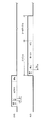
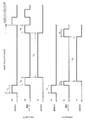
- FIG. 1 It is the schematic explanatory drawing of the film forming apparatus which concerns on one Embodiment of this invention. It is a figure which shows an example of the reaction gas activator shown in FIG. It is a figure which shows the CVD film and ALD film formed on the surface of the porous body which is the object of film formation. It is a timing chart of the film formation process in which the CVD process and the ALD process are continuous. It is a timing chart which shows the relationship between a CVD process and an ALD process.
- FIG. 1 shows a film-forming device according to an embodiment.
- the film forming apparatus 10 has, for example, a reaction vessel 20 made of quartz.
- the reaction vessel 20 has a raw material gas introduction port 30, a reaction gas introduction port 40, and an exhaust port 50.
- a support portion 60 for placing and supporting the film-forming object 1 is provided in the reaction vessel 20, for example.
- the first supply pipe 100 is connected to the raw material gas introduction port 30, and the raw material gas container 110 and the flow rate controller 130 are connected to the first supply pipe 100.
- the first valve 120 provided in the first supply pipe 100 is in the open state, the raw material gas of the flow rate controlled by the flow rate controller 130 is supplied from the raw material gas container 110 to the raw material gas introduction port 30.
- a second supply pipe 200 is connected to the reaction gas introduction port 40.
- the second supply pipe 200 is provided with a reaction gas activation device 210.
- the reaction gas container 220 supplies the reaction gas to the reaction gas activator 210.
- the reaction gas activated by the reaction gas activating device 210 is supplied to the reaction gas introduction port 40 via the second valve 230.
- the raw material gas is, for example, TDMAS (SiH [N (CH 3 ) 2 ] 3 ), the activated reaction gas is OH radical (OH * ), and the silicon oxide film SiO is set as the film forming target 1. 2 shall be formed.
- TDMAS SiH [N (CH 3 ) 2 ] 3
- the activated reaction gas is OH radical (OH * )
- the silicon oxide film SiO is set as the film forming target 1. 2 shall be formed.
- trimethylaluminum Al (CH 3 ) 3 used as a raw material gas may react with OH radical (OH * ) to form aluminum oxide Al 2 O 3 .
- FIG. 2A shows an example of the reaction gas container 220 and the reaction gas activator 210.
- the reaction gas is, for example, water vapor H 2 O, which activates water vapor to generate OH radicals (OH *).
- the reaction gas container 220 includes a humidifier 240 in which water 2 is stored and an inert gas container 250.
- an inert gas such as argon Ar from the inert gas container 250 is introduced through the pipe 260.
- the water 2 bubbled by the argon Ar becomes steam gas and is supplied to the second supply pipe 200.
- an induction coil 270 is provided around the second supply pipe 200 made of quartz.
- the high frequency power supply 212 shown in FIG. 1 is connected to the induction coil 270.
- the electromagnetic energy applied by the induction coil 270 is 20 W and the frequency is 13.56 MHz.
- the induction coil 270 generates inductively coupled plasma 3 of the reaction gas in the second supply pipe 200.
- An exhaust pipe 300 is connected to the exhaust port 50 of the reaction vessel 20, and the exhaust pipe 300 is provided with an exhaust pump 310 and an exhaust valve 320.
- the reaction vessel 20 can be evacuated by the exhaust pump 310. Thereby, the raw material gas or the reaction gas can be exhausted from the reaction vessel 20.
- an inert gas as a purge gas can be supplied to the reaction vessel 20 by controlling the flow rate during exhaust by the exhaust pump 310.
- the inside of the reaction vessel 20 may be replaced with the purge gas by introducing a purge gas.
- an inert gas may be used as the carrier gas of the raw material gas.
- the control unit 400 controls the CVD process and the ALD process.
- FIG. 3 is a schematic view showing an example of forming a film on the surface of the porous body 1 to be formed by the film forming method executed by the control unit 400.
- FIG. 4 is a timing chart of the film forming method executed by the control unit 400, in which the CVD process and the ALD process are continuously executed.
- FIG. 5 is a timing chart showing the relationship between the CVD process and the ALD process executed by the control unit 400.
- the control content of the control unit 400 will be described by taking the film forming method of the present embodiment as an example.
- the CVD film 4 is first formed, and then the ALD film 5 is formed on the CVD film 4.
- the CVD film 4 fills the pores 1A of the porous body 1, and the dense ALD film 5 can cover the CVD film 4 having a sparse density and poor barrier properties, for example.
- the surface of the porous body 1 can be modified into a surface having properties such as hydrophobicity or hydrophilicity, for example.
- the control unit 400 controls each part of the film forming apparatus 10 so that the CVD process is first carried out and then the ALD process is carried out. Moreover, the control unit 400 simplifies the control by standardizing the CVD process and the ALD process.
- the commonality between the CVD process and the ALD process is to adopt a CVD process similar to one cycle of the ALD cycle that is repeatedly executed in the ALD process. The commonality between the CVD process and the ALD process will be described with reference to FIG.
- the ALD process repeats an ALD cycle in which the first to fourth steps are one cycle until the film thickness of the ALD film 5 is obtained.
- the inside of the reaction vessel 20 is evacuated by the exhaust pump 310, and the inside of the reaction vessel 20 is set to, for example, 10 -4 Pa.
- the raw material gas TDMS is supplied into the reaction vessel 20 with the first valve 120 open, and the first valve 120 is closed.
- the inside of the reaction vessel 20 is filled with the raw material gas at a relatively low pressure, for example, 1 to 10 Pa.
- TDMAS is adsorbed on the surface of the film forming object 1 on the support portion 60.
- OH radical (OH * ) which is a reaction gas activated by the reaction gas activator 210, opens the second valve 230. Is introduced into the reaction vessel 20. After that, the second valve 230 is closed, and the inside of the reaction vessel 20 is filled with the reaction gas at a relatively low pressure.
- TDMAS reacts with OH radicals (OH * ) on the surface of the film-forming object 1.
- TDMAS is oxidized by OH radicals (OH * ) to form a silicon oxide film SiO 2 .
- the surface of the film-forming object 1 is covered with the silicon oxide film.
- a hydroxy group (-OH) is formed on the silicon oxide film.
- the organometallic gas can be saturated and adsorbed even at room temperature. Therefore, it is not necessary to forcibly heat the film forming object 1 during the film forming.
- the exhaust time T4 A of the fourth step can be made equal to, for example, the exhaust time T2 A of the second step.
- the ALD cycle composed of the first step to the fourth step is repeatedly carried out until the film thickness of the ALD film 5 is obtained.
- ozone may be filled in the reaction vessel 20 at a predetermined pressure, for example, 1 to 10 Pa, and then discharged with a purge gas before the raw material gas TDMAS is introduced into the reaction vessel 20. By introducing ozone, it is possible to prevent unreacted carbon from being mixed into the film.
- the CVD process also has a first step to a fourth step like the ALD cycle.
- the time of the first step is T1 C
- the time of the second step is T2 C
- the time of the third step is T3 C
- the time of the fourth step is T4 C
- T1 C T2 A
- the CVD process is set equal to the ALD cycle, except that the time T2 C of the second step is set shorter than the time T2 A of the second step of the ALD cycle.
- the control can be made extremely simple.
- the supply of the raw material gas in the first step and the supply of the activation reaction gas in the third step are separated not simultaneously but through the second step.
- the pressure of the raw material gas in the first step can be a relatively low pressure, for example, 1 to 10 Pa, which is the same as in the first step of the ALD cycle.
- the exhaust of the second step is terminated with the raw material gas remaining in the gas phase of the reaction vessel 20.
- the raw material gas remains in the gas phase of the reaction vessel 20 even after the exhaust in the second step, so that the activation reaction gas introduced into the reaction vessel 20 in the third step is the raw material in the gas phase. This is because it reacts with the gas to realize a chemical gas phase growth (CVD) process rather than an ALD process.
- CVD chemical gas phase growth
- the other one is to use a raw material gas whose pressure is lower than the introduction pressure of the reaction gas even by the exhaust of the second step without excessively increasing the pressure for introducing the activation reaction gas in the third step. This is to prevent backflow to the supply pipe 200 and the reaction gas activator 210.
- the pressure for introducing the activation reaction gas is a pressure at which plasma of the reaction gas can be generated in the reaction gas activating device 210, for example, 5 to 15 Pa.
- the first pressure P1 in the reaction vessel 20 after the second step is lower than the pressure P2 into which the activation reaction gas is introduced, the above-mentioned backflow can be prevented, and the second step is necessary for that purpose. Since the valve 230 is closed after the activation reaction gas is introduced, the raw material gas and the reaction gas do not react with each other in the second supply pipe 200 during the third step.
- a metal nitride film by using, for example, a nitride gas instead of the oxidation gas, which is a reaction gas used when forming a metal oxide film.
- a nitride gas instead of the oxidation gas, which is a reaction gas used when forming a metal oxide film.
- NH 3 in which NH radicals are generated can be used as the nitriding gas as the reaction gas.
- SiN can be formed by using, for example, TDMAS (SiH [N (CH 3 ) 2 ] 3 ) as the raw material gas, and TiN by using, for example, TDMAT (Ti [N (CH 3 ) 2 ] 4) as the raw material gas. Can be formed. In either case, the presence of NH radicals can realize a low temperature process.
Landscapes
- Chemical & Material Sciences (AREA)
- Engineering & Computer Science (AREA)
- Metallurgy (AREA)
- Chemical Kinetics & Catalysis (AREA)
- Materials Engineering (AREA)
- Mechanical Engineering (AREA)
- General Chemical & Material Sciences (AREA)
- Organic Chemistry (AREA)
- Physics & Mathematics (AREA)
- Plasma & Fusion (AREA)
- Inorganic Chemistry (AREA)
- Analytical Chemistry (AREA)
- Electromagnetism (AREA)
- Chemical Vapour Deposition (AREA)
Priority Applications (5)
| Application Number | Priority Date | Filing Date | Title |
|---|---|---|---|
| JP2021554934A JP7112793B2 (ja) | 2019-11-06 | 2020-11-02 | 成膜方法及び成膜装置 |
| CN202080076110.XA CN114651087A (zh) | 2019-11-06 | 2020-11-02 | 成膜方法及成膜装置 |
| EP20885070.1A EP4056731A4 (en) | 2019-11-06 | 2020-11-02 | Film formation method and film formation device |
| KR1020227018405A KR20220097444A (ko) | 2019-11-06 | 2020-11-02 | 성막 방법 및 성막 장치 |
| US17/735,897 US20220259732A1 (en) | 2019-11-06 | 2022-05-03 | Film formation method and film formation device |
Applications Claiming Priority (2)
| Application Number | Priority Date | Filing Date | Title |
|---|---|---|---|
| JP2019-201441 | 2019-11-06 | ||
| JP2019201441 | 2019-11-06 |
Related Child Applications (1)
| Application Number | Title | Priority Date | Filing Date |
|---|---|---|---|
| US17/735,897 Continuation US20220259732A1 (en) | 2019-11-06 | 2022-05-03 | Film formation method and film formation device |
Publications (1)
| Publication Number | Publication Date |
|---|---|
| WO2021090794A1 true WO2021090794A1 (ja) | 2021-05-14 |
Family
ID=75848503
Family Applications (1)
| Application Number | Title | Priority Date | Filing Date |
|---|---|---|---|
| PCT/JP2020/041016 Ceased WO2021090794A1 (ja) | 2019-11-06 | 2020-11-02 | 成膜方法及び成膜装置 |
Country Status (7)
| Country | Link |
|---|---|
| US (1) | US20220259732A1 (https=) |
| EP (1) | EP4056731A4 (https=) |
| JP (1) | JP7112793B2 (https=) |
| KR (1) | KR20220097444A (https=) |
| CN (1) | CN114651087A (https=) |
| TW (1) | TW202124761A (https=) |
| WO (1) | WO2021090794A1 (https=) |
Families Citing this family (2)
| Publication number | Priority date | Publication date | Assignee | Title |
|---|---|---|---|---|
| JP7039085B1 (ja) * | 2021-08-30 | 2022-03-22 | 株式会社クリエイティブコーティングス | 成膜装置 |
| CN113862644A (zh) * | 2021-09-22 | 2021-12-31 | 江苏微导纳米科技股份有限公司 | 镀膜设备 |
Citations (6)
| Publication number | Priority date | Publication date | Assignee | Title |
|---|---|---|---|---|
| JP2014135311A (ja) * | 2013-01-08 | 2014-07-24 | Ps4 Luxco S A R L | 半導体装置 |
| WO2014188927A1 (ja) * | 2013-05-21 | 2014-11-27 | ピーエスフォー ルクスコ エスエイアールエル | 半導体装置及びその製造方法 |
| WO2015145486A1 (ja) * | 2014-03-28 | 2015-10-01 | 国立大学法人東北大学 | プラズマ処理装置およびプラズマ処理方法 |
| JP2016131222A (ja) * | 2015-01-15 | 2016-07-21 | 国立大学法人山形大学 | 薄膜堆積方法 |
| US20180082886A1 (en) * | 2016-09-16 | 2018-03-22 | Lam Research Corporation | Temporally pulsed and kinetically modulated cvd dielectrics for gapfill applications |
| JP2018059173A (ja) | 2016-10-07 | 2018-04-12 | 東京エレクトロン株式会社 | 成膜方法 |
Family Cites Families (8)
| Publication number | Priority date | Publication date | Assignee | Title |
|---|---|---|---|---|
| US6482733B2 (en) | 2000-05-15 | 2002-11-19 | Asm Microchemistry Oy | Protective layers prior to alternating layer deposition |
| CN101657564A (zh) * | 2007-02-12 | 2010-02-24 | 莲花应用技术有限责任公司 | 用原子层沉积制备复合材料 |
| US8017182B2 (en) * | 2007-06-21 | 2011-09-13 | Asm International N.V. | Method for depositing thin films by mixed pulsed CVD and ALD |
| JP5513767B2 (ja) * | 2008-06-25 | 2014-06-04 | 株式会社日立国際電気 | 半導体装置の製造方法、基板処理方法、基板処理装置および半導体装置 |
| JP5801916B2 (ja) | 2008-06-25 | 2015-10-28 | 株式会社日立国際電気 | 半導体装置の製造方法、基板処理方法、および基板処理装置 |
| WO2013046157A1 (en) * | 2011-09-27 | 2013-04-04 | L'air Liquide, Societe Anonyme Pour L'etude Et L'exploitation Des Procedes Georges Claude | Nickel bis diazabutadiene precursors, their synthesis, and their use for nickel containing film depositions |
| EP2628817B1 (en) | 2012-02-15 | 2016-11-02 | IHI Hauzer Techno Coating B.V. | A coated article of martensitic steel and a method of forming a coated article of steel |
| US10573522B2 (en) * | 2016-08-16 | 2020-02-25 | Lam Research Corporation | Method for preventing line bending during metal fill process |
-
2020
- 2020-11-02 WO PCT/JP2020/041016 patent/WO2021090794A1/ja not_active Ceased
- 2020-11-02 CN CN202080076110.XA patent/CN114651087A/zh active Pending
- 2020-11-02 EP EP20885070.1A patent/EP4056731A4/en not_active Withdrawn
- 2020-11-02 JP JP2021554934A patent/JP7112793B2/ja not_active Expired - Fee Related
- 2020-11-02 KR KR1020227018405A patent/KR20220097444A/ko not_active Withdrawn
- 2020-11-05 TW TW109138560A patent/TW202124761A/zh unknown
-
2022
- 2022-05-03 US US17/735,897 patent/US20220259732A1/en not_active Abandoned
Patent Citations (6)
| Publication number | Priority date | Publication date | Assignee | Title |
|---|---|---|---|---|
| JP2014135311A (ja) * | 2013-01-08 | 2014-07-24 | Ps4 Luxco S A R L | 半導体装置 |
| WO2014188927A1 (ja) * | 2013-05-21 | 2014-11-27 | ピーエスフォー ルクスコ エスエイアールエル | 半導体装置及びその製造方法 |
| WO2015145486A1 (ja) * | 2014-03-28 | 2015-10-01 | 国立大学法人東北大学 | プラズマ処理装置およびプラズマ処理方法 |
| JP2016131222A (ja) * | 2015-01-15 | 2016-07-21 | 国立大学法人山形大学 | 薄膜堆積方法 |
| US20180082886A1 (en) * | 2016-09-16 | 2018-03-22 | Lam Research Corporation | Temporally pulsed and kinetically modulated cvd dielectrics for gapfill applications |
| JP2018059173A (ja) | 2016-10-07 | 2018-04-12 | 東京エレクトロン株式会社 | 成膜方法 |
Also Published As
| Publication number | Publication date |
|---|---|
| JPWO2021090794A1 (https=) | 2021-05-14 |
| JP7112793B2 (ja) | 2022-08-04 |
| EP4056731A1 (en) | 2022-09-14 |
| KR20220097444A (ko) | 2022-07-07 |
| TW202124761A (zh) | 2021-07-01 |
| EP4056731A4 (en) | 2023-08-30 |
| US20220259732A1 (en) | 2022-08-18 |
| CN114651087A (zh) | 2022-06-21 |
Similar Documents
| Publication | Publication Date | Title |
|---|---|---|
| TWI631232B (zh) | 藉由原子層沉積法形成順應性的氧化、氮化、或碳化介電膜的方法 | |
| US7745346B2 (en) | Method for improving process control and film conformality of PECVD film | |
| JP4396547B2 (ja) | 成膜方法、成膜装置及び記憶媒体 | |
| JP5651451B2 (ja) | 半導体装置の製造方法、基板処理方法及び基板処理装置 | |
| US9613798B2 (en) | Method of manufacturing semiconductor device, substrate processing apparatus, and recording medium | |
| JP6496510B2 (ja) | 半導体装置の製造方法、基板処理装置およびプログラム | |
| US20050223982A1 (en) | Apparatus and method for depositing thin film on wafer using remote plasma | |
| JPWO2005098922A1 (ja) | 半導体装置の製造方法 | |
| JP2007189173A (ja) | 成膜方法、成膜装置及び記憶媒体 | |
| US20150357181A1 (en) | Method of manufacturing semiconductor device, substrate processing apparatus, and recording medium | |
| TW201017758A (en) | Method of manufacturing semiconductor device and substrate processing apparatus | |
| KR102288228B1 (ko) | 반도체 장치의 제조 방법, 기판 처리 장치 및 프로그램 | |
| WO2005017987A1 (ja) | 基板処理装置及び半導体デバイスの製造方法 | |
| JP2011192875A (ja) | 半導体装置の製造方法及び基板処理装置 | |
| JP2017168788A (ja) | 半導体装置の製造方法、基板処理装置およびプログラム | |
| WO2021090794A1 (ja) | 成膜方法及び成膜装置 | |
| JP2013145796A (ja) | TiSiN膜の成膜方法および記憶媒体 | |
| JPWO2005024926A1 (ja) | 基板処理装置及び半導体装置の製造方法 | |
| JP2013147708A (ja) | TiSiN膜の成膜方法および記憶媒体 | |
| JP2017183392A (ja) | 基板処理装置、半導体装置の製造方法および記録媒体 | |
| KR100966928B1 (ko) | 성막 장치 및 성막 방법 | |
| JP2021080522A (ja) | 基板処理方法及び基板処理装置 | |
| JPS61234531A (ja) | シリコン酸化物の作製方法 | |
| JP4979965B2 (ja) | 基板処理装置及び半導体装置の製造方法 | |
| JP2006299407A (ja) | 成膜方法、成膜装置およびコンピュータ読取可能な記憶媒体 |
Legal Events
| Date | Code | Title | Description |
|---|---|---|---|
| 121 | Ep: the epo has been informed by wipo that ep was designated in this application |
Ref document number: 20885070 Country of ref document: EP Kind code of ref document: A1 |
|
| WWE | Wipo information: entry into national phase |
Ref document number: 2021554934 Country of ref document: JP |
|
| ENP | Entry into the national phase |
Ref document number: 20227018405 Country of ref document: KR Kind code of ref document: A |
|
| NENP | Non-entry into the national phase |
Ref country code: DE |
|
| ENP | Entry into the national phase |
Ref document number: 2020885070 Country of ref document: EP Effective date: 20220607 |
|
| WWW | Wipo information: withdrawn in national office |
Ref document number: 1020227018405 Country of ref document: KR |
|
| WWW | Wipo information: withdrawn in national office |
Ref document number: 2020885070 Country of ref document: EP |