WO2021090670A1 - 面発光レーザ装置 - Google Patents
面発光レーザ装置 Download PDFInfo
- Publication number
- WO2021090670A1 WO2021090670A1 PCT/JP2020/039329 JP2020039329W WO2021090670A1 WO 2021090670 A1 WO2021090670 A1 WO 2021090670A1 JP 2020039329 W JP2020039329 W JP 2020039329W WO 2021090670 A1 WO2021090670 A1 WO 2021090670A1
- Authority
- WO
- WIPO (PCT)
- Prior art keywords
- layer
- contact
- dbr
- emitting laser
- electrode layer
- Prior art date
- Legal status (The legal status is an assumption and is not a legal conclusion. Google has not performed a legal analysis and makes no representation as to the accuracy of the status listed.)
- Ceased
Links
Images















Classifications
-
- H—ELECTRICITY
- H01—ELECTRIC ELEMENTS
- H01S—DEVICES USING THE PROCESS OF LIGHT AMPLIFICATION BY STIMULATED EMISSION OF RADIATION [LASER] TO AMPLIFY OR GENERATE LIGHT; DEVICES USING STIMULATED EMISSION OF ELECTROMAGNETIC RADIATION IN WAVE RANGES OTHER THAN OPTICAL
- H01S5/00—Semiconductor lasers
- H01S5/02—Structural details or components not essential to laser action
- H01S5/022—Mountings; Housings
- H01S5/0239—Combinations of electrical or optical elements
-
- H—ELECTRICITY
- H01—ELECTRIC ELEMENTS
- H01S—DEVICES USING THE PROCESS OF LIGHT AMPLIFICATION BY STIMULATED EMISSION OF RADIATION [LASER] TO AMPLIFY OR GENERATE LIGHT; DEVICES USING STIMULATED EMISSION OF ELECTROMAGNETIC RADIATION IN WAVE RANGES OTHER THAN OPTICAL
- H01S5/00—Semiconductor lasers
- H01S5/02—Structural details or components not essential to laser action
- H01S5/0206—Substrates, e.g. growth, shape, material, removal or bonding
- H01S5/0208—Semi-insulating substrates
-
- H—ELECTRICITY
- H01—ELECTRIC ELEMENTS
- H01S—DEVICES USING THE PROCESS OF LIGHT AMPLIFICATION BY STIMULATED EMISSION OF RADIATION [LASER] TO AMPLIFY OR GENERATE LIGHT; DEVICES USING STIMULATED EMISSION OF ELECTROMAGNETIC RADIATION IN WAVE RANGES OTHER THAN OPTICAL
- H01S5/00—Semiconductor lasers
- H01S5/02—Structural details or components not essential to laser action
- H01S5/022—Mountings; Housings
- H01S5/0233—Mounting configuration of laser chips
- H01S5/0234—Up-side down mountings, e.g. Flip-chip, epi-side down mountings or junction down mountings
-
- H—ELECTRICITY
- H01—ELECTRIC ELEMENTS
- H01S—DEVICES USING THE PROCESS OF LIGHT AMPLIFICATION BY STIMULATED EMISSION OF RADIATION [LASER] TO AMPLIFY OR GENERATE LIGHT; DEVICES USING STIMULATED EMISSION OF ELECTROMAGNETIC RADIATION IN WAVE RANGES OTHER THAN OPTICAL
- H01S5/00—Semiconductor lasers
- H01S5/02—Structural details or components not essential to laser action
- H01S5/022—Mountings; Housings
- H01S5/0235—Method for mounting laser chips
- H01S5/02355—Fixing laser chips on mounts
- H01S5/0237—Fixing laser chips on mounts by soldering
-
- H—ELECTRICITY
- H01—ELECTRIC ELEMENTS
- H01S—DEVICES USING THE PROCESS OF LIGHT AMPLIFICATION BY STIMULATED EMISSION OF RADIATION [LASER] TO AMPLIFY OR GENERATE LIGHT; DEVICES USING STIMULATED EMISSION OF ELECTROMAGNETIC RADIATION IN WAVE RANGES OTHER THAN OPTICAL
- H01S5/00—Semiconductor lasers
- H01S5/04—Processes or apparatus for excitation, e.g. pumping, e.g. by electron beams
- H01S5/042—Electrical excitation ; Circuits therefor
- H01S5/0425—Electrodes, e.g. characterised by the structure
- H01S5/04252—Electrodes, e.g. characterised by the structure characterised by the material
-
- H—ELECTRICITY
- H01—ELECTRIC ELEMENTS
- H01S—DEVICES USING THE PROCESS OF LIGHT AMPLIFICATION BY STIMULATED EMISSION OF RADIATION [LASER] TO AMPLIFY OR GENERATE LIGHT; DEVICES USING STIMULATED EMISSION OF ELECTROMAGNETIC RADIATION IN WAVE RANGES OTHER THAN OPTICAL
- H01S5/00—Semiconductor lasers
- H01S5/04—Processes or apparatus for excitation, e.g. pumping, e.g. by electron beams
- H01S5/042—Electrical excitation ; Circuits therefor
- H01S5/0425—Electrodes, e.g. characterised by the structure
- H01S5/04254—Electrodes, e.g. characterised by the structure characterised by the shape
-
- H—ELECTRICITY
- H01—ELECTRIC ELEMENTS
- H01S—DEVICES USING THE PROCESS OF LIGHT AMPLIFICATION BY STIMULATED EMISSION OF RADIATION [LASER] TO AMPLIFY OR GENERATE LIGHT; DEVICES USING STIMULATED EMISSION OF ELECTROMAGNETIC RADIATION IN WAVE RANGES OTHER THAN OPTICAL
- H01S5/00—Semiconductor lasers
- H01S5/04—Processes or apparatus for excitation, e.g. pumping, e.g. by electron beams
- H01S5/042—Electrical excitation ; Circuits therefor
- H01S5/0425—Electrodes, e.g. characterised by the structure
- H01S5/04256—Electrodes, e.g. characterised by the structure characterised by the configuration
- H01S5/04257—Electrodes, e.g. characterised by the structure characterised by the configuration having positive and negative electrodes on the same side of the substrate
-
- H—ELECTRICITY
- H01—ELECTRIC ELEMENTS
- H01S—DEVICES USING THE PROCESS OF LIGHT AMPLIFICATION BY STIMULATED EMISSION OF RADIATION [LASER] TO AMPLIFY OR GENERATE LIGHT; DEVICES USING STIMULATED EMISSION OF ELECTROMAGNETIC RADIATION IN WAVE RANGES OTHER THAN OPTICAL
- H01S5/00—Semiconductor lasers
- H01S5/10—Construction or shape of the optical resonator, e.g. extended or external cavity, coupled cavities, bent-guide, varying width, thickness or composition of the active region
- H01S5/18—Surface-emitting [SE] lasers, e.g. having both horizontal and vertical cavities
- H01S5/183—Surface-emitting [SE] lasers, e.g. having both horizontal and vertical cavities having only vertical cavities, e.g. vertical cavity surface-emitting lasers [VCSEL]
- H01S5/18305—Surface-emitting [SE] lasers, e.g. having both horizontal and vertical cavities having only vertical cavities, e.g. vertical cavity surface-emitting lasers [VCSEL] with emission through the substrate, i.e. bottom emission
-
- H—ELECTRICITY
- H01—ELECTRIC ELEMENTS
- H01S—DEVICES USING THE PROCESS OF LIGHT AMPLIFICATION BY STIMULATED EMISSION OF RADIATION [LASER] TO AMPLIFY OR GENERATE LIGHT; DEVICES USING STIMULATED EMISSION OF ELECTROMAGNETIC RADIATION IN WAVE RANGES OTHER THAN OPTICAL
- H01S5/00—Semiconductor lasers
- H01S5/10—Construction or shape of the optical resonator, e.g. extended or external cavity, coupled cavities, bent-guide, varying width, thickness or composition of the active region
- H01S5/18—Surface-emitting [SE] lasers, e.g. having both horizontal and vertical cavities
- H01S5/183—Surface-emitting [SE] lasers, e.g. having both horizontal and vertical cavities having only vertical cavities, e.g. vertical cavity surface-emitting lasers [VCSEL]
- H01S5/18344—Surface-emitting [SE] lasers, e.g. having both horizontal and vertical cavities having only vertical cavities, e.g. vertical cavity surface-emitting lasers [VCSEL] characterized by the mesa, e.g. dimensions or shape of the mesa
- H01S5/18347—Mesa comprising active layer
-
- H—ELECTRICITY
- H01—ELECTRIC ELEMENTS
- H01S—DEVICES USING THE PROCESS OF LIGHT AMPLIFICATION BY STIMULATED EMISSION OF RADIATION [LASER] TO AMPLIFY OR GENERATE LIGHT; DEVICES USING STIMULATED EMISSION OF ELECTROMAGNETIC RADIATION IN WAVE RANGES OTHER THAN OPTICAL
- H01S5/00—Semiconductor lasers
- H01S5/10—Construction or shape of the optical resonator, e.g. extended or external cavity, coupled cavities, bent-guide, varying width, thickness or composition of the active region
- H01S5/18—Surface-emitting [SE] lasers, e.g. having both horizontal and vertical cavities
- H01S5/183—Surface-emitting [SE] lasers, e.g. having both horizontal and vertical cavities having only vertical cavities, e.g. vertical cavity surface-emitting lasers [VCSEL]
- H01S5/18361—Structure of the reflectors, e.g. hybrid mirrors
- H01S5/18375—Structure of the reflectors, e.g. hybrid mirrors based on metal reflectors
-
- H—ELECTRICITY
- H01—ELECTRIC ELEMENTS
- H01S—DEVICES USING THE PROCESS OF LIGHT AMPLIFICATION BY STIMULATED EMISSION OF RADIATION [LASER] TO AMPLIFY OR GENERATE LIGHT; DEVICES USING STIMULATED EMISSION OF ELECTROMAGNETIC RADIATION IN WAVE RANGES OTHER THAN OPTICAL
- H01S5/00—Semiconductor lasers
- H01S5/10—Construction or shape of the optical resonator, e.g. extended or external cavity, coupled cavities, bent-guide, varying width, thickness or composition of the active region
- H01S5/18—Surface-emitting [SE] lasers, e.g. having both horizontal and vertical cavities
- H01S5/183—Surface-emitting [SE] lasers, e.g. having both horizontal and vertical cavities having only vertical cavities, e.g. vertical cavity surface-emitting lasers [VCSEL]
- H01S5/18361—Structure of the reflectors, e.g. hybrid mirrors
- H01S5/18377—Structure of the reflectors, e.g. hybrid mirrors comprising layers of different kind of materials, e.g. combinations of semiconducting with dielectric or metallic layers
-
- H—ELECTRICITY
- H01—ELECTRIC ELEMENTS
- H01S—DEVICES USING THE PROCESS OF LIGHT AMPLIFICATION BY STIMULATED EMISSION OF RADIATION [LASER] TO AMPLIFY OR GENERATE LIGHT; DEVICES USING STIMULATED EMISSION OF ELECTROMAGNETIC RADIATION IN WAVE RANGES OTHER THAN OPTICAL
- H01S5/00—Semiconductor lasers
- H01S5/40—Arrangement of two or more semiconductor lasers, not provided for in groups H01S5/02 - H01S5/30
- H01S5/42—Arrays of surface emitting lasers
- H01S5/423—Arrays of surface emitting lasers having a vertical cavity
-
- G—PHYSICS
- G01—MEASURING; TESTING
- G01S—RADIO DIRECTION-FINDING; RADIO NAVIGATION; DETERMINING DISTANCE OR VELOCITY BY USE OF RADIO WAVES; LOCATING OR PRESENCE-DETECTING BY USE OF THE REFLECTION OR RERADIATION OF RADIO WAVES; ANALOGOUS ARRANGEMENTS USING OTHER WAVES
- G01S17/00—Systems using the reflection or reradiation of electromagnetic waves other than radio waves, e.g. lidar systems
- G01S17/02—Systems using the reflection of electromagnetic waves other than radio waves
- G01S17/06—Systems determining position data of a target
- G01S17/08—Systems determining position data of a target for measuring distance only
-
- G—PHYSICS
- G01—MEASURING; TESTING
- G01S—RADIO DIRECTION-FINDING; RADIO NAVIGATION; DETERMINING DISTANCE OR VELOCITY BY USE OF RADIO WAVES; LOCATING OR PRESENCE-DETECTING BY USE OF THE REFLECTION OR RERADIATION OF RADIO WAVES; ANALOGOUS ARRANGEMENTS USING OTHER WAVES
- G01S17/00—Systems using the reflection or reradiation of electromagnetic waves other than radio waves, e.g. lidar systems
- G01S17/88—Lidar systems specially adapted for specific applications
- G01S17/93—Lidar systems specially adapted for specific applications for anti-collision purposes
- G01S17/931—Lidar systems specially adapted for specific applications for anti-collision purposes of land vehicles
-
- G—PHYSICS
- G01—MEASURING; TESTING
- G01S—RADIO DIRECTION-FINDING; RADIO NAVIGATION; DETERMINING DISTANCE OR VELOCITY BY USE OF RADIO WAVES; LOCATING OR PRESENCE-DETECTING BY USE OF THE REFLECTION OR RERADIATION OF RADIO WAVES; ANALOGOUS ARRANGEMENTS USING OTHER WAVES
- G01S7/00—Details of systems according to groups G01S13/00, G01S15/00, G01S17/00
- G01S7/48—Details of systems according to groups G01S13/00, G01S15/00, G01S17/00 of systems according to group G01S17/00
- G01S7/481—Constructional features, e.g. arrangements of optical elements
- G01S7/4814—Constructional features, e.g. arrangements of optical elements of transmitters alone
-
- H—ELECTRICITY
- H01—ELECTRIC ELEMENTS
- H01S—DEVICES USING THE PROCESS OF LIGHT AMPLIFICATION BY STIMULATED EMISSION OF RADIATION [LASER] TO AMPLIFY OR GENERATE LIGHT; DEVICES USING STIMULATED EMISSION OF ELECTROMAGNETIC RADIATION IN WAVE RANGES OTHER THAN OPTICAL
- H01S2301/00—Functional characteristics
- H01S2301/17—Semiconductor lasers comprising special layers
- H01S2301/176—Specific passivation layers on surfaces other than the emission facet
-
- H—ELECTRICITY
- H01—ELECTRIC ELEMENTS
- H01S—DEVICES USING THE PROCESS OF LIGHT AMPLIFICATION BY STIMULATED EMISSION OF RADIATION [LASER] TO AMPLIFY OR GENERATE LIGHT; DEVICES USING STIMULATED EMISSION OF ELECTROMAGNETIC RADIATION IN WAVE RANGES OTHER THAN OPTICAL
- H01S5/00—Semiconductor lasers
- H01S5/02—Structural details or components not essential to laser action
- H01S5/028—Coatings ; Treatment of the laser facets, e.g. etching, passivation layers or reflecting layers
- H01S5/0287—Facet reflectivity
-
- H—ELECTRICITY
- H01—ELECTRIC ELEMENTS
- H01S—DEVICES USING THE PROCESS OF LIGHT AMPLIFICATION BY STIMULATED EMISSION OF RADIATION [LASER] TO AMPLIFY OR GENERATE LIGHT; DEVICES USING STIMULATED EMISSION OF ELECTROMAGNETIC RADIATION IN WAVE RANGES OTHER THAN OPTICAL
- H01S5/00—Semiconductor lasers
- H01S5/10—Construction or shape of the optical resonator, e.g. extended or external cavity, coupled cavities, bent-guide, varying width, thickness or composition of the active region
- H01S5/18—Surface-emitting [SE] lasers, e.g. having both horizontal and vertical cavities
- H01S5/183—Surface-emitting [SE] lasers, e.g. having both horizontal and vertical cavities having only vertical cavities, e.g. vertical cavity surface-emitting lasers [VCSEL]
- H01S5/18308—Surface-emitting [SE] lasers, e.g. having both horizontal and vertical cavities having only vertical cavities, e.g. vertical cavity surface-emitting lasers [VCSEL] having a special structure for lateral current or light confinement
- H01S5/18311—Surface-emitting [SE] lasers, e.g. having both horizontal and vertical cavities having only vertical cavities, e.g. vertical cavity surface-emitting lasers [VCSEL] having a special structure for lateral current or light confinement using selective oxidation
-
- H—ELECTRICITY
- H01—ELECTRIC ELEMENTS
- H01S—DEVICES USING THE PROCESS OF LIGHT AMPLIFICATION BY STIMULATED EMISSION OF RADIATION [LASER] TO AMPLIFY OR GENERATE LIGHT; DEVICES USING STIMULATED EMISSION OF ELECTROMAGNETIC RADIATION IN WAVE RANGES OTHER THAN OPTICAL
- H01S5/00—Semiconductor lasers
- H01S5/30—Structure or shape of the active region; Materials used for the active region
- H01S5/34—Structure or shape of the active region; Materials used for the active region comprising quantum well or superlattice structures, e.g. single quantum well [SQW] lasers, multiple quantum well [MQW] lasers or graded index separate confinement heterostructure [GRINSCH] lasers
- H01S5/343—Structure or shape of the active region; Materials used for the active region comprising quantum well or superlattice structures, e.g. single quantum well [SQW] lasers, multiple quantum well [MQW] lasers or graded index separate confinement heterostructure [GRINSCH] lasers in AIIIBV compounds, e.g. AlGaAs-laser, InP-based laser
- H01S5/34313—Structure or shape of the active region; Materials used for the active region comprising quantum well or superlattice structures, e.g. single quantum well [SQW] lasers, multiple quantum well [MQW] lasers or graded index separate confinement heterostructure [GRINSCH] lasers in AIIIBV compounds, e.g. AlGaAs-laser, InP-based laser with a well layer having only As as V-compound, e.g. AlGaAs, InGaAs
Definitions
- This disclosure relates to a surface emitting laser device.
- a DBR diffractive Bragg Reflector
- the surface emitting laser apparatus is provided at a position facing the active layer, the first DBR layer and the second DBR layer sandwiching the active layer, and the light emitting region of the active layer, and is viewed from the active layer. It includes an insulating film and a metal layer corresponding to the end portion of the reflection mirror on the second DBR layer side.
- This surface emitting laser device is further in contact with the first contact layer provided in the first DBR layer or in contact with the first DBR layer, the second contact layer provided in contact with the second DBR layer, and the first contact layer. It is provided with a first electrode layer provided in the above direction and a second electrode layer provided in contact with the second contact layer and at a position not opposed to the light emitting region of the active layer.
- an insulating film and a metal layer are provided at the end of the reflection mirror on the second DBR layer side when viewed from the active layer.
- the first DBR layer, the second DBR layer, the insulating film, and the metal layer cause laser oscillation at a predetermined oscillation wavelength.
- laser oscillation at a predetermined oscillation wavelength can be generated, so that the number of pairs of the second DBR layer is reduced. The resistance during driving is reduced by that amount.
- the first electrode layer is further provided in contact with the first contact layer provided in the first DBR layer or in contact with the first DBR layer, and is a second body separate from the metal layer.
- the electrode layer is provided in contact with the second contact layer.
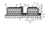
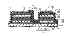
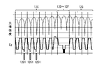
- FIG. 2 It is a figure which shows the plane structure example of the surface emitting laser apparatus which concerns on one Embodiment of this disclosure. It is a figure which shows the example of the cross-sectional structure in line AA of FIG. It is a figure which shows the example of the cross-sectional structure of the emitter of FIG. 2 and its surroundings. (A) It is a figure which shows the plane structure example when the bump is omitted on the upper surface of the emitter of FIG. (B) It is a figure which shows the plane structure example when the metal layer is omitted in FIG. 4 (A). It is a figure which shows the structural example of the insulating film which covers the mesa part of FIG.
- FIG. 3 is an enlarged view showing a cross-sectional configuration example of the emitter of FIG.
- FIG. 3 is an enlarged view showing a cross-sectional configuration example of the emitter of FIG.
- FIG. 3 is an enlarged view showing a cross-sectional configuration example of the emitter of FIG.
- FIG. 3 is an enlarged view showing a cross-sectional configuration example of the emitter of FIG.
- FIG. 3 is an enlarged view showing a cross-sectional configuration example of the emitter of FIG.
- FIG. 3 is an enlarged view showing a cross-sectional configuration example of the emitter of FIG. It is a figure which shows the plane structure example when the laser driver IC of FIG. 1 is mounted on a printed wiring board. It is a figure which shows the example of the cross-sectional structure in line AA of FIG. It is sectional drawing which shows an example of the manufacturing method of the laser chip of FIG. It is sectional drawing which shows an example of the manufacturing process following FIG. It is sectional drawing which shows an example of the manufacturing process following FIG. It is sectional drawing which shows an example of the manufacturing process following FIG. It is sectional drawing which shows an example of the manufacturing process following FIG. It is sectional drawing which shows an example of the manufacturing process following FIG. It is sectional drawing which shows an example of the manufacturing process following FIG. It is sectional drawing which shows an example of the manufacturing process following FIG. It is sectional drawing which shows an example of the manufacturing process following FIG. It is sectional drawing which shows an example of the manufacturing process following FIG. It is sectional drawing which shows an example of the manufacturing process
- FIG. 1 It is sectional drawing which shows an example of the manufacturing process following FIG. It is sectional drawing which shows an example of the manufacturing process following FIG. It is a figure which shows the cross-sectional composition example of the DBR near the upper surface of the emitter of FIG. It is a figure which shows one modification of the cross-sectional structure of the emitter of FIG. 2 and its surroundings. It is a figure which shows an example of the light field intensity and the energy level of each layer in the mesa part of FIG. It is a figure which shows the application example to the distance measuring apparatus of the surface emitting laser apparatus which concerns on the said Embodiment and the modification. It is a block diagram which shows an example of the schematic structure of a vehicle control system. It is explanatory drawing which shows an example of the installation position of the distance measuring apparatus.
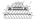
- FIG. 1 shows an example of a top surface configuration of the surface emitting laser device 1.
- FIG. 2 shows an example of cross-sectional configuration of the surface emitting laser device 1 of FIG. 1 taken along the line AA.
- the surface emitting laser device 1 is a back-emission type laser that can be suitably applied to applications that are thin and require low power consumption, applications that are thin and require a large area, and the like.
- the surface emitting laser device 1 includes a laser chip 10 and a laser driver IC 20.
- the laser chip 10 is arranged on the laser driver IC 20.
- the laser chip 10 is electrically connected to the laser driver IC 20 via, for example, a plurality of bumps 14.
- the laser chip 10 includes, for example, a substrate 13, an emitter array 11 formed on the surface of the substrate 13 on the laser driver IC 20 side, and a plurality of bumps 14 formed on the surface of the substrate 13 on the laser driver IC 20 side.
- the substrate 13 has an AR (Anti-reflection) layer 13A formed on a surface (light emitting surface) opposite to the laser driver IC 20.
- the emitter array 11 is arranged on the side opposite to the light emitting surface of the substrate 13.
- the AR layer 13A is composed of, for example, a laminated body in which SiO 2 and SiN are laminated.
- the emitter array 11 is composed of a plurality of emitters 12 arranged on the same substrate 13, for example, as shown in FIGS. 1 and 2.
- the plurality of emitters 12 are arranged on the substrate 13 at equal intervals in the row direction and at equal intervals in the column direction, for example.
- the plurality of emitters 12 may be randomly arranged on the same substrate 13.
- Each emitter 12 is composed of a surface emitting type semiconductor laser that emits laser light in the stacking direction. In the present embodiment, each emitter 12 emits laser light to the side opposite to the laser driver IC 20 via the substrate 13 and the AR layer 13A.
- the substrate 13 is composed of, for example, a semi-insulating semiconductor substrate (for example, a Si—GaAs substrate) that transmits light emitted from the emitter 12.
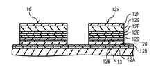
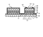
- the etching stop layer 12B, the DBR layer 12C, the spacer layer 12D, the active layer 12E, the spacer layer 12F, the DBR layer 12G, and the contact layer 12H are sequentially arranged from the substrate 13 side. It has a columnar vertical resonator structure (mesa portion 12x) formed by stacking.
- the diameter (mesa diameter) of each mesa portion 12x is slightly smaller than the beam pitch of the laser beam emitted from each mesa portion 12x. For example, when the beam pitch is set to about 18 ⁇ m, the diameter (mesa diameter) of each mesa portion 12x is about 14 ⁇ m.
- each emitter 12 has a contact layer 12A in contact with the etching stop layer 12B.
- the contact layer 12A is a layer for ohmic contacting each mesa portion 12x (specifically, the DBR layer 12C described later) and the electrode layer 17 described later with each other.
- the contact layer 12A is provided between each mesa portion 12x and the substrate 13, and is in contact with each mesa portion 12x and the substrate 13.
- the substrate 13 is provided in contact with the contact layer 12A on the side opposite to the active layer 12E.
- the contact layer 12A corresponds to a specific example of the "first contact layer" of the present disclosure.
- the contact layer 12H corresponds to a specific example of the "second contact layer” of the present disclosure.
- the contact layer 12A is shared by each emitter 12. That is, the plurality of mesa portions 12x are arranged on the same contact layer 12A, and in the laser chip 10, each mesa portion 12x projects toward the laser driver IC 20 side.
- the contact layer 12H is an end face on the laser driver IC 20 side.
- the end face of the mesa portion 12x on the laser driver IC20 side may be referred to as the upper surface of the mesa portion 12x for convenience.
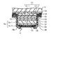
- a current constriction layer 12I is provided in the DBR layer 12G. Note that FIG. 3 shows an example of cross-sectional configuration of the portion of the laser chip 10 shown in FIG. 2 surrounded by a broken line.
- each mesa portion 12x is formed by, for example, a substrate 13 as a crystal growth substrate.
- Each mesa portion 12x contact layer 12A is made of, for example, a GaAs-based semiconductor.
- the contact layer 12A is composed of, for example, p-type Al x1 Ga 1-x1 As (0 ⁇ x1 ⁇ 1).
- the etching stop layer 12B is composed of, for example, p-type In x2 Ga 1-x2 P (0 ⁇ x2 ⁇ 1).
- the DBR layer 12C is formed by alternately laminating low refractive index layers (not shown) and high refractive index layers (not shown).
- the low refractive index layer is composed of, for example, p-type Al x3 Ga 1-x3 As (0 ⁇ x3 ⁇ 1) having an optical thickness of ⁇ ⁇ 1/4 ( ⁇ 1 is an oscillation wavelength), and is a high refractive index layer. Consists of, for example, p-type Al x4 Ga 1-x4 As (0 ⁇ x4 ⁇ x3) having an optical thickness of ⁇ ⁇ 1/4.
- the spacer layer 12D is made of, for example, p-type Al x5 Ga 1-x5 As (0 ⁇ x5 ⁇ 1).
- the contact layer 12A, the etching stop layer 12B, the DBR layer 12C, and the spacer layer 12D contain p-type impurities such as carbon (C). That is, the contact layer 12A, the etching stop layer 12B, the DBR layer 12C, and the spacer layer 12D are made of a p-type semiconductor.
- the active layer 12E is, for example, from a well layer (not shown) consisting of undoped In x6 Ga 1-x6 As (0 ⁇ x6 ⁇ 1) and undoped In x7 Ga 1-x7 As (0 ⁇ x7 ⁇ x6). It has a multiple quantum well structure in which barrier layers (not shown) are alternately laminated.
- the region of the active layer 12E facing the current injection region 12I-1 (described later) is the light emitting region.
- the spacer layer 12F is made of, for example, n-type Al x8 Ga 1-x8 As (0 ⁇ x8 ⁇ 1).
- the DBR layer 12G is formed by alternately laminating low refractive index layers (not shown) and high refractive index layers (not shown).
- the low refractive index layer is composed of, for example, n-type Al x9 Ga 1-x9 As (0 ⁇ x9 ⁇ 1) having an optical thickness of ⁇ ⁇ 1/4
- the high refractive index layer is, for example, having an optical thickness of ⁇ ⁇ 1/4. It is composed of ⁇ ⁇ 1/4 n-type Al x10 Ga 1-x10 As (0 ⁇ x10 ⁇ x9).
- the contact layer 12H is a layer for ohmic contacting the DBR layer 12G and the ring electrode layer 12K with each other.
- the contact layer 12H is composed of, for example, n-type Al x11 Ga 1-x11 As (0 ⁇ x11 ⁇ 1).
- the spacer layer 12F, the DBR layer 12G, and the contact layer 12H contain n-type impurities such as silicon (Si). That is, the spacer layer 12F, the DBR layer 12G, and the contact layer 12H are made of an n-type semiconductor.
- the number of pairs of the low refractive index layer and the high refractive index layer in the DBR layer 12G is smaller than, for example, the number of pairs of the low refractive index layer and the high refractive index layer in the DBR layer 12C.
- the number of pairs of the DBR layer 12G is less than half the number of pairs required as the DBR layer when the insulating film 15a and the metal layer 12L described later are not provided. This is because the insulating film 15a and the metal layer 12L assist the light reflection function of the DBR layer 12G, and the low refractive index of the DBR layer 12G is due to the light reflection ability of the insulating film 15a and the metal layer 12L. This is because the number of pairs of the rate layer and the high refractive index layer can be reduced.
- the current constriction layer 12I has a current injection region 12I-1 and a current constriction region 12I-2.
- the current constriction region 12I-2 is formed in the peripheral region of the current injection region 12I-1.
- the current injection region 12I-1 is composed of, for example, p-type Al x12 Ga 1-x12 As (0 ⁇ x12 ⁇ 1).
- the current constriction region 12I-2 is configured to contain, for example, Al 2 O 3 (aluminum oxide), and for example, by oxidizing a high concentration of Al contained in the oxidized layer 12M (described later) from the side surface. can get. Therefore, the current constriction layer 12I has a function of constricting the current.
- Each emitter 12 further has a ring electrode layer 12K in contact with the contact layer 12H, for example, as shown in FIGS. 3 and 4B. That is, the ring electrode layer 12K is arranged on the side opposite to the light emitting surface of the substrate 13 and is formed in contact with the upper surface of the mesa portion 12x.
- the ring electrode layer 12K corresponds to a specific example of the "second electrode layer" of the present disclosure.
- the ring electrode layer 12K is formed at a position not opposed to the light emitting region (or current injection region 12I-1) of the active layer 12E, and faces the light emitting region (or current injection region 12I-1) of the active layer 12E.
- the ring electrode layer 12K is in contact with a portion of the contact layer 12H that is not opposed to the light emitting region (or current injection region 12I-1) of the active layer 12E. Therefore, the ring electrode layer 12K is electrically connected to the DBR layer 12G via the contact layer 12H.
- the ring electrode layer 12K is composed of an alloy.
- the ring electrode layer 12K is composed of, for example, an alloy that is in contact with the contact layer 12H, and is, for example, a laminated body formed by laminating AuGe, Ni, and Au in order from the contact layer 12H side.
- Each emitter 12 further has a metal layer 12L in contact with the ring electrode layer 12K, for example, as shown in FIGS. 3 and 4A.
- the metal layer 12L corresponds to a specific example of the "metal layer" of the present disclosure.
- the metal layer 12L is formed so as to close the opening of the ring electrode layer 12K, and the outer edge portion (the portion not opposed to the current injection region 12I-1) of the metal layer 12L is in contact with the ring electrode layer 12K. Therefore, the metal layer 12L is electrically connected to the DBR layer 12G via the ring electrode layer 12K and the contact layer 12H.
- the metal layer 12L is also in contact with the bump 14, and is electrically connected to the laser driver IC 20 via the bump 14.
- the metal layer 12L is, for example, electrically connected to an NMOS in the laser driver IC 20.
- the metal layer 12L is made of a non-alloy, and is, for example, a laminated body formed by laminating Ti, Pt, and Au in order from the ring electrode layer 12K side.
- the bump 14 is composed of, for example, Au.
- the metal layer 12L is not in direct contact with the upper surface (contact layer 12H) of the mesa portion 12x.
- the central portion of the metal layer 12L (the portion facing the current injection region 12I-1) is laminated on the upper surface (contact layer 12H) of the mesa portion 12x via the insulating film 15a described later.
- the central portion of the metal layer 12L and the insulating film 15a are provided at positions facing the light emitting region (or current injection region 12I-1) of the active layer 12E, and are reflected on the DBR layer 12G side when viewed from the active layer 12E. Corresponds to the end of the mirror.
- the portion in contact with the upper surface (contact layer 12H) of the mesa portion 12x corresponds to a specific example of the "insulating film" of the present disclosure.
- Each emitter 12 further has an electrode layer 17 in contact with the contact layer 12A, for example, as shown in FIG.
- the electrode layer 17 corresponds to a specific example of the “first electrode layer” of the present disclosure.
- the electrode layer 17 is arranged on the side opposite to the light emitting surface of the substrate 13, and is in contact with the contact layer 12A at a position not opposed to the mesa portion 12x.
- the electrode layer 17 is in contact with, for example, a portion of the contact layer 12A corresponding to the skirt of the mesa portion 12x. Therefore, the electrode layer 17 is electrically connected to the DBR layer 12C via the contact layer 12A.
- the electrode layer 17 is made of a non-alloy, and is, for example, a laminated body formed by laminating Ti, Pt, and Au in order from the contact layer 12A side.
- Each emitter 12 further has insulating films 15a and 15b that protect the mesa portion 12x, for example, as shown in FIG.
- the insulating film 15a covers the side surface of the mesa portion 12x, and has an opening in the portion of the mesa portion 12x facing the ring electrode layer 12K (FIG. 4B).
- the insulating film 15a further covers a portion of the mesa portion 12x that is exposed in the opening of the ring electrode layer 12K (exposed portion 12H1 in FIG. 4B), and constitutes a pedestal of the electrode layer 18 described later. (Pedestal portion 16) is also covered.
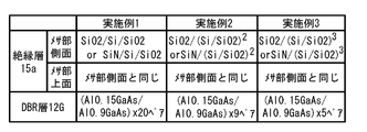
- the insulating film 15a is composed of a laminated body in which SiO 2 , Si, and SiO 2 are laminated in this order from the side surface side of the mesa portion 12x, for example.
- the insulating film 15a may be composed of a laminated body in which SiN, Si, and SiO 2 are laminated in this order from the side surface side of the mesa portion 12x, for example, as shown in the first embodiment of FIG. SiN helps to suppress the invasion of moisture from the outside.
- the SiN (SiN layer) contained in the insulating film 15a is in contact with the side surface of the mesa portion 12x. Further, for example, as shown in the first embodiment of FIG.
- the insulating film 15a is composed of a laminated body in which SiO 2 , Si, and SiO 2 are laminated in this order from the upper surface side of the mesa portion 12x.
- the insulating film 15a may be composed of a laminated body in which SiN, Si, and SiO 2 are laminated in this order from the upper surface side of the mesa portion 12x, for example, as shown in the first embodiment of FIG.
- the insulating film 15a has, for example, the same layer structure as each other on the side surface and the upper surface of the mesa portion 12x.
- the insulating film 15a is composed of a laminated body in which SiO 2 , Si, SiO 2 , Si, and SiO 2 are laminated in this order from the side surface side of the mesa portion 12x, for example. You may.
- the insulating film 15a is composed of a laminated body in which SiN, Si, SiO 2 , Si, and SiO 2 are laminated in this order from the side surface side of the mesa portion 12x, for example. May be good.
- the SiN (SiN layer) contained in the insulating film 15a is in contact with the side surface of the mesa portion 12x. Further, for example, as shown in the second embodiment of FIG.
- the insulating film 15a is composed of a laminated body in which SiO 2 , Si, SiO 2 , Si, SiO 2 are laminated in this order from the upper surface side of the mesa portion 12x. It may have been done. As shown in Example 2 of FIG. 5, the insulating film 15a is composed of a laminated body in which SiN, Si, SiO 2 , Si, and SiO 2 are laminated in this order from the upper surface side of the mesa portion 12x. May be good.
- the insulating film 15a has, for example, the same layer structure as each other on the side surface and the upper surface of the mesa portion 12x.
- the insulating film 15a can play the role of a reflection mirror, and the high refractive index layer and the high refractive index layer contained in DBR12G
- the number of pairs of the low refractive index layer can be reduced to about half (for example, 9 pairs) as compared with Example 1.
- the insulating film 15a is laminated in the order of SiO 2 , Si, SiO 2 , Si, SiO 2 , Si, SiO 2 from the side surface side of the mesa portion 12x. It may be composed of a body. As shown in Example 3 of FIG. 5, the insulating film 15a is a laminate in which SiN, Si, SiO 2 , Si, SiO 2 , Si, and SiO 2 are laminated in this order from the side surface side of the mesa portion 12x. It may be composed of. At this time, the SiN (SiN layer) contained in the insulating film 15a is in contact with the side surface of the mesa portion 12x.
- the insulating film 15a is further laminated in the order of SiO 2 , Si, SiO 2 , Si, SiO 2 , Si, SiO 2 from the upper surface side of the mesa portion 12x, for example, as shown in Example 3 of FIG. It may be composed of a laminated body. As shown in Example 3 of FIG. 5, the insulating film 15a is a laminate in which SiN, Si, SiO 2 , Si, SiO 2 , Si, and SiO 2 are laminated in this order from the upper surface side of the mesa portion 12x. It may be composed of.
- the insulating film 15a has, for example, the same layer structure as each other on the side surface and the upper surface of the mesa portion 12x.
- the insulating film 15a can play the role of a reflection mirror, and the high refractive index layer and the high refractive index layer contained in DBR12G
- the number of pairs of the low refractive index layer can be reduced to about one-fourth (for example, five pairs) as compared with Example 1.
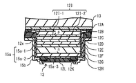
- the insulating film 15a may be composed of a laminated body in which SiN, SiO 2 , Si, and SiO 2 are laminated in this order from the side surface side of the mesa portion 12x. .. At this time, the SiN (SiN layer) contained in the insulating film 15a is in contact with the side surface of the mesa portion 12x. Further, for example, as shown in the fourth embodiment of FIG. 6, the insulating film 15a may be further composed of a laminated body in which SiO 2 , Si, and SiO 2 are laminated in this order from the upper surface side of the mesa portion 12x. .. In Example 4 of FIG. 6, for example, as shown in FIG.
- the insulating film 15a has a SiN layer 15a-1 in contact with the side surface of the mesa portion 12x and a SiN layer 15a-1 on the side surface side of the mesa portion 12x. It is composed of a laminated body (laminated body in which SiO 2 , Si, SiO 2 is laminated in this order) 15a-2 in contact with.
- the insulating film 15a is further formed as a laminate (SiO 2 , Si, SiO) in contact with the upper surface side of the mesa portion 12x on the upper surface side of the mesa portion 12x, for example, as shown in FIG. It is composed of (laminated body) 15a-3 laminated in the order of 2.
- the laminates 15a-2 and 15a-3 are collectively formed, for example, in the same process.
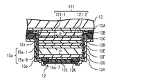
- the insulating film 15a is composed of a laminated body in which SiN, SiO 2 , Si, SiO 2 , Si, and SiO 2 are laminated in this order from the side surface side of the mesa portion 12x. It may have been. At this time, the SiN (SiN layer) contained in the insulating film 15a is in contact with the side surface of the mesa portion 12x. Further, for example, as shown in Example 5 of FIG. 6, the insulating film 15a is composed of a laminate in which SiO 2 , Si, SiO 2 , Si, SiO 2 are laminated in this order from the upper surface side of the mesa portion 12x. It may have been done. In Example 5 of FIG.
- the insulating film 15a has a SiN layer 15a-1 in contact with the side surface of the mesa portion 12x and a SiN layer 15a-1 on the side surface side of the mesa portion 12x. It is composed of a laminated body (a laminated body in which SiO 2 , Si, SiO 2 , Si, SiO 2 are laminated in this order) 15a-4 in contact with.
- the insulating film 15a is further formed as a laminate (SiO 2 , Si, SiO) in contact with the upper surface side of the mesa portion 12x on the upper surface side of the mesa portion 12x, for example, as shown in FIG.
- the insulating film 15a can play the role of a reflection mirror, and the high refractive index layer and the high refractive index layer contained in DBR12G The number of pairs of the low refractive index layer can be reduced to about half (for example, 9 pairs) as compared with Example 1.
- the insulating film 15a is laminated in the order of SiN, SiO 2 , Si, SiO 2 , Si, SiO 2 , Si, SiO 2 from the side surface side of the mesa portion 12x. It may be composed of a laminated body. At this time, the SiN (SiN layer) contained in the insulating film 15a is in contact with the side surface of the mesa portion 12x.
- the insulating film 15a is further laminated in the order of SiO 2 , Si, SiO 2 , Si, SiO 2 , Si, SiO 2 from the upper surface side of the mesa portion 12x, for example, as shown in Example 6 of FIG. It may be composed of a laminated body.
- the insulating film 15a has a SiN layer 15a-1 in contact with the side surface of the mesa portion 12x and a SiN layer 15a-1 on the side surface side of the mesa portion 12x. It is composed of a laminated body (a laminated body in which SiO 2 , Si, SiO 2 , Si, SiO 2 , Si, SiO 2 are laminated in this order) 15a-6 in contact with.
- a laminated body a laminated body in which SiO 2 , Si, SiO 2 , Si, SiO 2 , Si, SiO 2 are laminated in this order
- the insulating film 15a is further formed as a laminate (SiO 2 , Si, SiO) in contact with the upper surface side of the mesa portion 12x on the upper surface side of the mesa portion 12x, for example, as shown in FIG. 2 , Si, SiO 2 , Si, SiO 2 are laminated in this order) 15a-7.
- the laminates 15a-6 and 15a-7 are collectively formed, for example, in the same process.
- the insulating film 15a can play the role of a reflection mirror, and the high refractive index layer and the high refractive index layer contained in DBR12G
- the number of pairs of the low refractive index layer can be reduced to about one-fourth (for example, five pairs) as compared with Example 1.
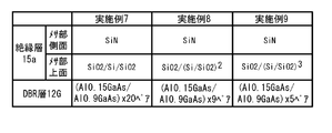
- the insulating film 15a may be composed of, for example, a SiN layer in contact with the side surface of the mesa portion 12x, as shown in Example 7 of FIG. At this time, the SiN (SiN layer) contained in the insulating film 15a is in contact with the side surface of the mesa portion 12x. Further, for example, as shown in Example 7 of FIG. 10, the insulating film 15a may be composed of a laminate in which SiO 2 , Si, and SiO 2 are laminated in this order from the upper surface side of the mesa portion 12x. .. In Example 7 of FIG.
- the insulating film 15a is composed of a SiN layer 15a-1 in contact with the side surface of the mesa portion 12x on the side surface side of the mesa portion 12x, for example, as shown in FIG.
- the insulating film 15a is further formed as a laminate (SiO 2 , Si, SiO) in contact with the upper surface side of the mesa portion 12x on the upper surface side of the mesa portion 12x, for example, as shown in FIG. It is composed of (laminated body) 15a-3 laminated in the order of 2.
- the insulating film 15a may be composed of, for example, a SiN layer in contact with the side surface of the mesa portion 12x, as shown in Example 8 of FIG. At this time, the SiN (SiN layer) contained in the insulating film 15a is in contact with the side surface of the mesa portion 12x. Further, for example, as shown in Example 8 of FIG. 10, the insulating film 15a is composed of a laminate in which SiO 2 , Si, SiO 2 , Si, SiO 2 are laminated in this order from the upper surface side of the mesa portion 12x. It may have been done. In Example 8 of FIG.
- the insulating film 15a is composed of a SiN layer 15a-1 in contact with the side surface of the mesa portion 12x on the side surface side of the mesa portion 12x, for example, as shown in FIG.
- the insulating film 15a is further formed as a laminate (SiO 2 , Si, SiO) in contact with the upper surface side of the mesa portion 12x on the upper surface side of the mesa portion 12x, for example, as shown in FIG. 2 , Si, SiO 2 are laminated in this order) 15a-8.
- the insulating film 15a may be composed of, for example, a SiN layer in contact with the side surface of the mesa portion 12x, as shown in Example 9 of FIG. At this time, the SiN (SiN layer) contained in the insulating film 15a is in contact with the side surface of the mesa portion 12x.
- the insulating film 15a is further laminated in the order of SiO 2 , Si, SiO 2 , Si, SiO 2 , Si, SiO 2 from the upper surface side of the mesa portion 12x, for example, as shown in Example 9 of FIG. It may be composed of a laminated body. In Example 9 of FIG.
- the insulating film 15a is composed of a SiN layer 15a-1 in contact with the side surface of the mesa portion 12x on the side surface side of the mesa portion 12x, for example, as shown in FIG.
- the insulating film 15a is further formed as a laminate (SiO 2 , Si, SiO) in contact with the upper surface side of the mesa portion 12x on the upper surface side of the mesa portion 12x, for example, as shown in FIG. 2 , Si, SiO 2 are laminated in this order) 15a-9.
- the insulating film 15b is in contact with the surface of the insulating film 15a at least a part of the side surface of the mesa portion 12x, and has an opening in the portion of the mesa portion 12x facing the ring electrode layer 12K and the metal layer 12L. ..
- the insulating film 15b further covers the connecting layer 19 described later.
- the insulating film 15b is made of, for example, a SiN film.
- the laser chip 10 has a pedestal portion 16 and an electrode layer 18 on the side opposite to the light emitting surface of the substrate 13 and around the emitter array 11. ing.
- the electrode layer 18 is formed on the surface of the pedestal portion 16 having the same structure as the vertical resonator structure of the mesa portion 12x on the laser driver IC 20 side.
- the electrode layer 18 corresponds to a specific example of the “third electrode layer” of the present disclosure.
- the laser chip 10 has a connecting layer 19 that electrically connects the electrode layer 17 and the electrode layer 18 to each other.
- the connecting layer 19 corresponds to a specific example of the "connecting layer" of the present disclosure.
- the connecting layer 19 extends from the upper surface of the pedestal portion 16 to the base of each emitter 12 via the side surface of the pedestal portion 16 and is connected to the electrode layer 17 and the electrode layer 18. Therefore, the electrode layer 18 is electrically connected to the DBR layer 12C of each emitter via the connecting layer 19, the electrode layer 17, and the contact layer 12A.
- the electrode layer 18 is also in contact with the bump 14, and is electrically connected to the laser driver IC 20 via the bump 14.
- the electrode layer 18 has, for example, the same potential as the reference potential of the laser driver IC 20.
- the electrode layer 18 is, for example, a laminated body formed by laminating Ti, Pt, and Au in this order from the upper surface side of the pedestal portion 16.
- the connecting layer 19 is, for example, an Au plating layer.
- the laser driver IC 20 is provided so as to face the surfaces of the plurality of emitters 12 of the laser chip 10.
- the laser driver IC 20 is electrically connected to the ring electrode layer 12K and the electrode layer 18 of each emitter 12 via a plurality of bumps 14, and the plurality of bumps 14, the ring electrode layer 12K, and the electrode layer 18 are connected to each other.
- the light emission / quenching of each emitter 12 is controlled via the light emission / extinction.
- the laser driver IC 20 independently drives a plurality of emitters 12 provided on the laser chip 10 to cause a part or all of the plurality of emitters 12 to emit light.
- the laser driver IC 20 drives, for example, a part or all of the emitters 12 selected by the system controller 30 described later among the plurality of emitters 12.
- the laser driver IC 20 has, for example, a Si substrate 21 and a wiring layer 22 formed on the Si substrate 21.
- the laser driver IC 20 has an NMOS driver on the Si substrate 21 that controls the voltage applied to the laser chip 10. This NMOS driver generates drive pulses for emitting and extinguishing a plurality of emitters 12 provided on the laser chip 10. The NMOS driver is electrically connected to the laser chip 10 via the wiring layer 22.
- the wiring layer 22 has, for example, a plurality of metal layers 22a, a plurality of connection pads 22c, and a plurality of connection pads 22d in the insulating layer 22b.
- the plurality of metal layers 22a electrically connect the NMOS driver in the Si substrate 21 and the plurality of connection pads 22d to each other.
- the plurality of connection pads 22d are arranged at positions of the wiring layer 22 facing the laser chip 10, and are electrically connected to the plurality of bumps 14 provided on the laser chip 10.
- the plurality of connection pads 22c are arranged at positions of the wiring layer 22 that are not opposed to the laser chip 10, and are electrically connected to, for example, the bonding wire 54 described later.
- the electrical connection mode between the laser chip 10 and the laser driver IC 20 is not limited to the description in FIG.
- FIG. 14 shows an example of a plan configuration when the laser driver IC 20 is mounted on the printed wiring board 40.
- the printed wiring board 40 is provided with, for example, a system controller 30 in addition to the laser driver IC 20.
- FIG. 15 shows an example of a cross-sectional configuration taken along the line AA of FIG.
- a bonding layer 43 is provided between the laser driver IC 20 and the printed wiring board 40. The bonding layer 43 fixes the laser driver IC 20 and the printed wiring board 40 to each other.
- the bonding layer 43 is made of, for example, a resin material having an insulating property.
- the laser driver IC 20 and the printed wiring board 40 are electrically connected by a bonding wire 44.
- One end of the bonding wire 44 is fixed to the connection pad 22c of the laser driver IC 20 by the solder 25, and the other end of the bonding wire 44 is fixed to the connection pad 41 of the printed wiring board 40 by the solder 42. There is.
- compound semiconductors are collectively formed on a substrate 13 made of GaAs, for example, by an epitaxial crystal growth method such as a MOCVD (Metal Organic Chemical Vapor Deposition) method. ..
- MOCVD Metal Organic Chemical Vapor Deposition
- raw materials for the compound semiconductor for example, methylaluminum (TMAl), trimethylgallium (TMGa), trimethylindium (TMIn) and other methyl-based organometallic gases and arsine (AsH 3 ) gas are used as donor impurities.
- As a raw material for example, disilane (Si 2 H 6 )
- As a raw material for acceptor impurities for example, carbon tetrabromide (CBr 4 ) is used.
- a contact layer 12A, an etching stop layer 12B, a DBR layer 12C including an oxidized layer 12M, a spacer layer 12D, an active layer 12E, and a spacer layer 12F are subjected to an epitaxial crystal growth method such as the MOCVD method.
- DBR layer 12G and contact layer 12H are formed in this order (FIG. 16).
- the contact layer 12H, the DBR layer 12G, the spacer layer 12F, the active layer 12E, the spacer layer 12D and the DBR layer 12C is selectively etched.
- RIE reactive Ion Etching
- Cl-based gas Cl-based gas
- an oxidation treatment is performed at a high temperature to selectively oxidize Al contained in the oxidized layer 12M from the side surface of the mesa portion 12x.
- Al contained in the oxidized layer 12M is selectively oxidized from the side surface of the mesa portion 12x by a wet oxidation method.
- the outer edge region of the oxidized layer 12M becomes an insulating layer (aluminum oxide), and the current constriction layer 12I is formed (FIG. 18).
- a ring electrode layer 12K is formed on the upper surface of the mesa portion 12x (FIG. 19). Subsequently, for example, after forming an insulating film 15a having an opening in the portion facing the ring electrode layer 12K and the skirt portion of the mesa portion 12x by using CVD or the like, for example, by using vapor deposition or sputtering or the like, the insulating film 15a is formed. The electrode layer 17 is formed in the opening provided in the skirt portion of the mesa portion 12x of the insulating film 15a (FIGS. 20 and 21).
- a metal layer 12L is formed on the upper surface of the mesa portion 12x so as to close the opening of the ring electrode layer 12K, and an electrode layer 18 is formed on the pedestal portion 16 (. FIG. 22).
- a plurality of emitters 12 are formed on the contact layer 12A.
- a plating method is used to form a connecting layer 19 that connects the electrode layer 17 of each emitter 12 and the electrode layer 18 on the pedestal portion 16 (FIG. 23).
- a base layer to be a seed for plating is formed in a portion of the insulating film 15a where the connecting layer 19 is to be formed, for example, by thin-film deposition or sputtering.
- the thickness of the connecting layer 19 is a thickness (for example, about 2 ⁇ m) that can sufficiently prevent a voltage drop.
- the substrate 13 is thinned using a grinder or the like, and then the AR layer 13A is formed on the back surface of the substrate 13 by using, for example, CVD or sputtering. Finally, the substrate 13 is diced. In this way, the laser chip 10 is manufactured.
- the insulating film 15a and the metal layer 12L are provided at the end of the reflection mirror on the DBR layer 12G side when viewed from the active layer 12E.
- the DBR layers 12C and 12G, the insulating film 15a, and the metal layer 12L cause laser oscillation at a predetermined oscillation wavelength.
- laser oscillation at a predetermined oscillation wavelength can be generated, so that the number of pairs of the DBR layer 12G is reduced. The resistance during driving is reduced by that amount.
- the electrode layer 17 is further provided in contact with the contact layer 12A provided in contact with the DBR layer 12C, and the ring electrode layer 12K separate from the metal layer 12L is the contact layer. It is provided in contact with 12H.
- the resistance during driving becomes smaller than when the electrode layer 17 is in contact with the contact layer 12A via the conductive semiconductor substrate.
- an alloy having a low contact resistance can be used as the material of the ring electrode layer 12K, compared with the case where a non-alloy suitable for the material of the reflection mirror is used as the material of the ring electrode layer 12K, it is during driving. The resistance becomes smaller. As described above, in the present embodiment, the resistance at the time of driving can be reduced. Further, by providing the ring electrode layer 12K, the drive voltage can be lowered and the IV characteristics can be improved.
- the metal layer 12L is in contact with the ring electrode layer 12K.
- the bump 14 and the ring electrode layer 12K can be electrically connected to each other via the metal layer 12L.
- the metal layer 12L can also be used as a pad electrode for the bump 14, the degree of integration of the emitter 12 is increased as compared with the case where the pad electrode for the bump 14 is provided separately from the metal layer 12L. Can be high. Further, by increasing the degree of integration of the emitter 12, it is possible to reduce the resistance caused by the wiring routing.
- the insulating film 15a is formed in the opening of the ring electrode layer 12K, and the metal layer 12L is formed so as to close the opening of the ring electrode layer 12K.
- the end portion (insulating film 15a and the insulating film 15a) of the reflection mirror on the DBR layer 12G side as viewed from the active layer 12E is located at a position facing the light emitting region (or current injection region 12I-1) of the active layer 12E.
- the metal layer 12L) can be provided, and an electrical contact with the DBR layer 12G can be provided at a position opposite to the light emitting region (or the current injection region 12I-1) of the active layer 12E.
- the degree of integration of the emitter 12 can be increased as compared with the case where the pad electrode for the bump 14 is provided at a position different from each emitter 12. Further, by increasing the degree of integration of the emitter 12, it is possible to reduce the resistance caused by the wiring routing.
- the electrode layer 17 is in contact with the contact layer 12A at a position not opposed to the mesa portion 12x.
- the ring electrode layer 12K on the mesa portion 12x and the electrode layer 17 on the contact layer 12A can be arranged on the side opposite to the light emitting surface of the substrate 13.
- the wiring space for electrically connecting the laser chip 10 and the laser driver IC 20 can be reduced as compared with the case where the ring electrode layer 12K and the electrode layer 17 are arranged so as to face each other with the substrate 13 in between. Therefore, the degree of integration of the emitter 12 can be increased. Further, by increasing the degree of integration of the emitter 12, it is possible to reduce the resistance caused by the wiring routing.
- a pedestal portion 16 including a structure common to the mesa portion 12x is provided on the side of the substrate 13 opposite to the light emitting surface, and the electrode layer 18 on the pedestal portion 16 and the contact layer 12A.
- a connecting layer 19 is provided which electrically connects the electrode layer 17 of the above to the electrode layer 17.
- the laser chip 10 and the laser driver IC 20 are bonded to each other via the bump 14, so that the laser chip 10 and the laser driver IC 20 can be easily electrically connected.
- the resistance caused by the wiring can be reduced as compared with the case where the laser chip 10 and the laser driver IC 20 are electrically connected by using wire bonding or the like.
- the connecting layer 19 thickly with a plating layer, the wiring resistance of the connecting layer 19 can be reduced.
- the laser driver IC 20 is arranged in the laser chip 10 so as to face the surface on the side of the plurality of emitters 12, and the laser driver IC 20 causes the plurality of bumps 14 and the ring electrode layer of each emitter 12.
- Light emission / quenching of each emitter 12 is controlled via 12K and the electrode layer 18 on the pedestal portion 16. Thereby, the light emission / quenching of each emitter 12 can be controlled with a small wiring resistance.
- the DBR layer 12C is composed of a p-type semiconductor
- the DBR layer 12G is composed of an n-type semiconductor.
- the laser driver IC 20 can be configured to include an NMOS driver that controls light emission / quenching of each emitter 12.
- the response speed of the laser driver IC 20 can be increased as compared with the case where the polyclonal driver is used. Therefore, the surface emitting laser device 1 can be suitably used for applications that require high-speed response of the driver.
- the SiN layer in contact with the side surface of the mesa portion 12x when the SiN layer in contact with the side surface of the mesa portion 12x is provided, it is possible to suppress the invasion of water into the mesa portion 12x from the outside. As a result, deterioration (for example, increasing resistance) of the mesa portion 12x due to moisture can be suppressed.
- FIG. 25 shows a modified example of the cross-sectional configuration of the DBR layer 12G in each emitter 12.
- the DBR layer 12G has, for example, a low-doping layer 12G1 having a relatively low doping amount at a position closer to the active layer 12E, as shown in FIG. 25, and the low-doping layer 12G1.
- a high-doping layer 12G2 having a relatively high doping amount may be provided at a position distant from the active layer 12E as compared with the above.
- the optical loss due to the doped impurities can be suppressed low in the vicinity of the active layer 12E of the DBR layer 12G, and at a position of the DBR layer 12G away from the active layer 12E. , High resistance can be suppressed.
- both suppression of optical loss and reduction of resistance can be achieved at the same time.
- FIG. 26 shows a modified example of the cross-sectional structure of the laser chip 10.
- a plurality of contact layers 12C1 may be provided instead of the contact layer 12A.
- the substrate 13 is provided in contact with the DBR layer 12C.
- the mesa portion 12x contains a part of the DBR layer 12C.
- the plurality of contact layers 12C1 are layers for ohmic contacting each mesa portion 12x (specifically, the DBR layer 12C) and the electrode layer 17 with each other.
- the contact layer 12C1 is composed of, for example, p-type Al x1 Ga 1-x1 As (0 ⁇ x1 ⁇ 1). In this case, the resistance during driving can be reduced by the amount that the plurality of contact layers 12C1 approach the active layer 12E.
- the contact layer 12C1 has not only the role of the contact layer but also the role of promoting the conduction of the electric current in the horizontal direction. Therefore, it is preferable that the contact layer 12C1 is doped with p-type impurities such as carbon at a high concentration (for example, 2 ⁇ 10 19 [1 / cm 3 ]). Usually, a layer with a high impurity concentration causes optical loss. However, in this modification, the plurality of contact layers 12C1 are provided at locations where the light field intensity (standing wave during resonance) is relatively low, for example, as shown in FIG. 27. Therefore, the optical loss caused by each contact layer 12C1 is limited. As described above, in this modification, both low resistance and high light output can be achieved at the same time.
- the etching stop layer 12C2 may be provided instead of the etching stop layer 12B.
- the etching stop layer 12C2 is provided in, for example, the DBR layer 12C, and is in contact with the layer closest to the DBR layer 12C among the plurality of contact layers 12C1.
- the etching stop layer 12C2 by utilizing the selective etching by the etching stop layer 12C2, the layer closest to the DBR layer 12C among the plurality of contact layers 12C1 can be reliably exposed, and the exposed contact layer 12C1 can be exposed.
- the electrode layer 17 can be reliably brought into contact with each other.
- a region (contact region 12N) in which impurities are doped at a high concentration may be provided at a portion of the DBR layer 12C facing the electrode layer 17.
- the contact region 12N is formed by, for example, using ion implantation to diffuse Zn with respect to a portion of the DBR layer 12C facing the electrode layer 17.
- the electrode layer 17 and the contact layer 12C1 can be electrically connected with low resistance. Thereby, the resistance at the time of driving can be reduced.
- FIG. 28 shows an example of a schematic configuration of a distance measuring device 100 provided with a surface emitting laser device 1.
- the distance measuring device 100 measures the distance to the subject 200 by the TOF (Time Of Flight) method.
- the distance measuring device 100 includes a surface emitting laser device 1 as a light source.
- the distance measuring device 100 includes, for example, a surface emitting laser device 1, a light receiving device 120, lenses 110 and 130, a signal processing unit 140, a control unit 150, a display unit 160, and a storage unit 170.
- the light receiving device 120 detects the light reflected by the subject 200.
- the lens 110 is a lens for collimating the light emitted from the surface emitting laser device 1 into parallel light, and is a collimating lens.
- the lens 130 is a lens for condensing the light reflected by the subject 200 and guiding it to the light receiving device 120, and is a condensing lens.
- the signal processing unit 140 is a circuit for generating a signal corresponding to the difference between the signal input from the light receiving device 120 and the reference signal input from the control unit 150.
- the control unit 150 includes, for example, a Time to Digital Converter (TDC).
- the reference signal may be a signal input from the control unit 150, or may be an output signal of the detection unit that directly detects the output of the surface emitting laser device 1.
- the control unit 150 is, for example, a processor that controls a surface emitting laser device 1, a light receiving device 120, a signal processing unit 140, a display unit 160, and a storage unit 170.
- the control unit 150 is a circuit that measures the distance to the subject 200 based on the signal generated by the signal processing unit 140.
- the control unit 150 generates a video signal for displaying information about the distance to the subject 200, and outputs the video signal to the display unit 160.
- the display unit 160 displays information about the distance to the subject 200 based on the video signal input from the control unit 150.
- the control unit 150 stores information about the distance to the subject 200 in the storage unit 170.
- the surface emitting laser device 1 is applied to the distance measuring device 100.
- the distance measuring device 100 can be used with low power consumption.
- FIG. 29 is a block diagram showing a schematic configuration example of a vehicle control system, which is an example of a mobile control system to which the technology according to the present disclosure can be applied.
- the vehicle control system 12000 includes a plurality of electronic control units connected via the communication network 12001.
- the vehicle control system 12000 includes a drive system control unit 12010, a body system control unit 12020, an outside information detection unit 12030, an in-vehicle information detection unit 12040, and an integrated control unit 12050.
- a microcomputer 12051, an audio image output unit 12052, and an in-vehicle network I / F (interface) 12053 are shown as a functional configuration of the integrated control unit 12050.
- the drive system control unit 12010 controls the operation of the device related to the drive system of the vehicle according to various programs.
- the drive system control unit 12010 provides a driving force generator for generating the driving force of the vehicle such as an internal combustion engine or a driving motor, a driving force transmission mechanism for transmitting the driving force to the wheels, and a steering angle of the vehicle. It functions as a control device such as a steering mechanism for adjusting and a braking device for generating a braking force of a vehicle.
- the body system control unit 12020 controls the operation of various devices mounted on the vehicle body according to various programs.
- the body system control unit 12020 functions as a keyless entry system, a smart key system, a power window device, or a control device for various lamps such as headlamps, back lamps, brake lamps, blinkers or fog lamps.
- the body system control unit 12020 may be input with radio waves transmitted from a portable device that substitutes for the key or signals of various switches.
- the body system control unit 12020 receives inputs of these radio waves or signals and controls a vehicle door lock device, a power window device, a lamp, and the like.
- the vehicle outside information detection unit 12030 detects information outside the vehicle equipped with the vehicle control system 12000.
- a distance measuring device 12031 is connected to the vehicle outside information detection unit 12030.
- the distance measuring device 12031 includes the above-mentioned distance measuring device 100.
- the vehicle outside information detection unit 12030 causes the distance measuring device 12031 to measure the distance to the object (subject 200) outside the vehicle, and acquires the distance data obtained thereby.
- the vehicle exterior information detection unit 12030 may perform object detection processing such as a person, a vehicle, an obstacle, or a sign based on the acquired distance data.
- the in-vehicle information detection unit 12040 detects the in-vehicle information.
- a driver state detection unit 12041 that detects the driver's state is connected to the in-vehicle information detection unit 12040.
- the driver state detection unit 12041 includes, for example, a camera that images the driver, and the in-vehicle information detection unit 12040 determines the degree of fatigue or concentration of the driver based on the detection information input from the driver state detection unit 12041. It may be calculated, or it may be determined whether the driver is dozing.
- the microcomputer 12051 calculates the control target value of the driving force generator, the steering mechanism, or the braking device based on the information inside and outside the vehicle acquired by the vehicle exterior information detection unit 12030 or the vehicle interior information detection unit 12040, and the drive system control unit.
- a control command can be output to 12010.
- the microcomputer 12051 realizes ADAS (Advanced Driver Assistance System) functions including vehicle collision avoidance or impact mitigation, follow-up driving based on inter-vehicle distance, vehicle speed maintenance driving, vehicle collision warning, vehicle lane deviation warning, and the like. It is possible to perform cooperative control for the purpose of.
- ADAS Advanced Driver Assistance System
- the microcomputer 12051 controls the driving force generator, the steering mechanism, the braking device, and the like based on the information around the vehicle acquired by the vehicle exterior information detection unit 12030 or the vehicle interior information detection unit 12040, so that the driver can control the driver. It is possible to perform coordinated control for the purpose of automatic driving, etc., which runs autonomously without depending on the operation.
- the microcomputer 12051 can output a control command to the body system control unit 12020 based on the information outside the vehicle acquired by the vehicle exterior information detection unit 12030.
- the microcomputer 12051 controls the headlamps according to the position of the preceding vehicle or the oncoming vehicle detected by the external information detection unit 12030, and performs coordinated control for the purpose of anti-glare such as switching the high beam to the low beam. It can be carried out.
- the audio image output unit 12052 transmits the output signal of at least one of the audio and the image to the output device capable of visually or audibly notifying the passenger or the outside of the vehicle of the information.
- an audio speaker 12061, a display unit 12062, and an instrument panel 12063 are exemplified as output devices.
- the display unit 12062 may include, for example, at least one of an onboard display and a heads-up display.
- FIG. 30 is a diagram showing an example of the installation position of the distance measuring device 12031.
- the vehicle 12100 has a distance measuring device 12101, 12102, 12103, 12104, 12105 as a distance measuring device 12031.
- the distance measuring devices 12101, 12102, 12103, 12104, 12105 are provided, for example, at positions such as the front nose, side mirrors, rear bumpers, back doors, and the upper part of the windshield in the vehicle interior of the vehicle 12100.
- the distance measuring device 12101 provided on the front nose and the distance measuring device 12105 provided on the upper part of the windshield in the vehicle interior mainly acquire data in front of the vehicle 12100.
- the distance measuring devices 12102 and 12103 provided in the side mirrors mainly acquire the data on the side of the vehicle 12100.
- the distance measuring device 12104 provided in the rear bumper or the back door mainly acquires the data behind the vehicle 12100.
- the data in front acquired by the distance measuring devices 12101 and 12105 is mainly used for detecting a preceding vehicle or a pedestrian, an obstacle, a traffic light, a traffic sign, or the like.
- FIG. 30 shows an example of the detection range of the distance measuring devices 12101 to 12104.
- the detection range 12111 indicates the detection range of the distance measuring device 12101 provided on the front nose
- the detection ranges 12112 and 12113 indicate the detection range of the distance measuring devices 12102 and 12103 provided on the side mirrors, respectively.
- the microcomputer 12051 is based on the distance data obtained from the distance measuring devices 12101 to 12104, and the distance to each three-dimensional object within the detection range 12111 to 12114 and the temporal change of this distance (relative velocity with respect to the vehicle 12100). ), In particular, the closest three-dimensional object on the traveling path of the vehicle 12100, which travels in substantially the same direction as the vehicle 12100 at a predetermined speed (for example, 0 km / h or more) is extracted as the preceding vehicle. Can be done. Further, the microcomputer 12051 can set an inter-vehicle distance to be secured in front of the preceding vehicle in advance, and can perform automatic braking control (including follow-up stop control), automatic acceleration control (including follow-up start control), and the like. In this way, it is possible to perform cooperative control for the purpose of automatic driving or the like in which the vehicle travels autonomously without depending on the operation of the driver.
- automatic braking control including follow-up stop control
- automatic acceleration control including follow-up start control
- the microcomputer 12051 uses the distance data obtained from the distance measuring devices 12101 to 12104 to obtain three-dimensional object data related to a three-dimensional object, such as a two-wheeled vehicle, an ordinary vehicle, a large vehicle, a pedestrian, and an electric pole. It can be classified into and extracted and used for automatic avoidance of obstacles. For example, the microcomputer 12051 distinguishes obstacles around the vehicle 12100 into obstacles that can be seen by the driver of the vehicle 12100 and obstacles that are difficult to see. Then, the microcomputer 12051 determines the collision risk indicating the risk of collision with each obstacle, and when the collision risk is equal to or higher than the set value and there is a possibility of collision, the microcomputer 12051 via the audio speaker 12061 or the display unit 12062. By outputting an alarm to the driver and performing forced deceleration and avoidance steering via the drive system control unit 12010, driving support for collision avoidance can be provided.
- three-dimensional object data related to a three-dimensional object such as a two-wheeled vehicle, an ordinary vehicle, a
- the above is an example of a mobile control system to which the technology according to the present disclosure can be applied.
- the technique according to the present disclosure can be applied to the distance measuring device 12031 among the configurations described above. By applying the technique according to the present disclosure to the distance measuring device 12031, the distance measuring device 12031 can be used with low power consumption.
- the present disclosure may have the following structure.
- the metal layer is made of a non-alloy
- the surface emitting laser apparatus according to (1) which includes the second electrode layer and an alloy.
- the surface emitting laser apparatus according to (1) or (2) wherein the metal layer is in contact with the second electrode layer.
- the second electrode layer is a ring electrode layer having an opening at a position facing the light emitting region of the active layer.
- the insulating film is formed in the opening of the second electrode layer, and is formed.
- the surface emitting laser device according to any one of (1) to (3), wherein the metal layer is formed so as to close the opening of the second electrode layer.
- the surface emitting laser apparatus according to any one of (1) to (4) wherein the number of pairs of the second DBR layer is smaller than the number of pairs of the first DBR layer.
- the whole or a part of the first DBR layer and a mesa portion including the second DBR layer are further provided.
- the surface emitting laser device according to any one of (1) to (5), wherein the first electrode layer is in contact with the first contact layer at a position not opposed to the mesa portion.
- a semi-insulating semiconductor substrate which is provided in contact with the first DBR layer or the first contact layer on the side opposite to the active layer side and which transmits light emitted from the mesa portion is further provided.
- a pedestal portion including a structure common to the mesa portion and a pedestal portion.
- a third electrode layer provided on the pedestal portion and The surface emitting laser apparatus according to (7), further comprising a connecting layer that electrically connects the first electrode layer and the third electrode layer to each other.
- the connecting layer is a plating layer.
- a laser chip having a plurality of emitters, the pedestal portion, the third electrode, and the connecting layer, A driver IC provided so as to face the plurality of emitter-side surfaces of the laser chip is further provided.
- Each of the emitters includes the active layer, the first DBR layer, the second DBR layer, the insulating film, the metal layer, the first contact layer, the second contact layer, the first electrode layer and the second electrode layer.
- the driver IC is electrically connected to the second electrode layer of each of the emitters and the third electrode via a plurality of bumps, and the plurality of bumps, the second electrode layer of each of the emitters, and the driver IC.
- the surface emitting laser apparatus according to (8) or (9), which controls light emission / quenching of each of the emitters via the third electrode.
- the first DBR layer is composed of a p-type semiconductor and is composed of a p-type semiconductor.
- the second DBR layer is composed of an n-type semiconductor and is composed of an n-type semiconductor.
- the second DBR layer has a low-doping layer having a relatively low doping amount at a position closer to the active layer, and the doping amount is at a position distant from the active layer as compared with the low-doping layer.
- an insulating film and a metal layer are provided at the end of the reflection mirror on the second DBR layer side when viewed from the active layer, and the first electrode layer is the first DBR. Since the second electrode layer provided in the layer or in contact with the first contact layer provided in contact with the first DBR layer and provided separately from the metal layer is provided in contact with the second contact layer. The resistance during driving can be reduced.
- the effects of the present disclosure are not necessarily limited to the effects described herein, and may be any of the effects described herein.
Landscapes
- Physics & Mathematics (AREA)
- Condensed Matter Physics & Semiconductors (AREA)
- General Physics & Mathematics (AREA)
- Electromagnetism (AREA)
- Optics & Photonics (AREA)
- Semiconductor Lasers (AREA)
Priority Applications (3)
| Application Number | Priority Date | Filing Date | Title |
|---|---|---|---|
| EP20884831.7A EP4020724A4 (en) | 2019-11-06 | 2020-10-20 | SURFACE EMITTING LASER DEVICE |
| US17/761,443 US20220247153A1 (en) | 2019-11-06 | 2020-10-20 | Surface light-emission laser device |
| JP2021554866A JP7531511B2 (ja) | 2019-11-06 | 2020-10-20 | 面発光レーザ装置 |
Applications Claiming Priority (4)
| Application Number | Priority Date | Filing Date | Title |
|---|---|---|---|
| JP2019-201616 | 2019-11-06 | ||
| JP2019201616 | 2019-11-06 | ||
| JP2020-064016 | 2020-03-31 | ||
| JP2020064016 | 2020-03-31 |
Publications (1)
| Publication Number | Publication Date |
|---|---|
| WO2021090670A1 true WO2021090670A1 (ja) | 2021-05-14 |
Family
ID=75848249
Family Applications (1)
| Application Number | Title | Priority Date | Filing Date |
|---|---|---|---|
| PCT/JP2020/039329 Ceased WO2021090670A1 (ja) | 2019-11-06 | 2020-10-20 | 面発光レーザ装置 |
Country Status (4)
| Country | Link |
|---|---|
| US (1) | US20220247153A1 (https=) |
| EP (1) | EP4020724A4 (https=) |
| JP (1) | JP7531511B2 (https=) |
| WO (1) | WO2021090670A1 (https=) |
Cited By (3)
| Publication number | Priority date | Publication date | Assignee | Title |
|---|---|---|---|---|
| WO2023162463A1 (ja) | 2022-02-22 | 2023-08-31 | ソニーセミコンダクタソリューションズ株式会社 | 発光デバイスおよびVoS(VCSEL on Silicon)デバイス |
| WO2023176308A1 (ja) * | 2022-03-15 | 2023-09-21 | ソニーグループ株式会社 | 発光装置、測距装置及び車載装置 |
| JP2025158108A (ja) * | 2024-04-03 | 2025-10-16 | ツー-シックス デラウェア インコーポレイテッド | 短距離光通信のためのvcsel/pcsel光の多層導波路への結合 |
Families Citing this family (2)
| Publication number | Priority date | Publication date | Assignee | Title |
|---|---|---|---|---|
| US20230047126A1 (en) * | 2020-02-07 | 2023-02-16 | Sony Semiconductor Solutions Corporation | Light emitting device |
| US20230238775A1 (en) * | 2022-01-27 | 2023-07-27 | Lumentum Operations Llc | Manipulating beam divergence of multi-junction vertical cavity surface emitting laser |
Citations (14)
| Publication number | Priority date | Publication date | Assignee | Title |
|---|---|---|---|---|
| JPH06112587A (ja) * | 1992-08-06 | 1994-04-22 | Motorola Inc | 電流分布および光学モ−ドの分離制御可能なvcsel |
| US6570905B1 (en) * | 2000-11-02 | 2003-05-27 | U-L-M Photonics Gmbh | Vertical cavity surface emitting laser with reduced parasitic capacitance |
| JP2003258380A (ja) | 2002-03-01 | 2003-09-12 | Seiko Epson Corp | 面発光型発光素子およびその製造方法、光モジュール、光伝達装置 |
| JP2004529487A (ja) * | 2000-11-28 | 2004-09-24 | ハネウェル・インターナショナル・インコーポレーテッド | 単一モードvcsel用の多機能方法およびシステム |
| JP2004288674A (ja) * | 2003-03-19 | 2004-10-14 | Fuji Xerox Co Ltd | 面発光型半導体レーザおよびそれを用いた光通信システム |
| JP2005158922A (ja) * | 2003-11-25 | 2005-06-16 | Fuji Xerox Co Ltd | 表面発光型半導体レーザ素子およびその製造方法 |
| US20080069166A1 (en) * | 2006-09-14 | 2008-03-20 | Samsung Electronics Co.; Ltd | Vertical-cavity surface-emitting laser |
| JP2010050412A (ja) * | 2008-08-25 | 2010-03-04 | Sony Corp | 面発光型半導体レーザ |
| JP2012505541A (ja) * | 2008-10-14 | 2012-03-01 | コーニンクレッカ フィリップス エレクトロニクス エヌ ヴィ | 改善したモード選択度を持つ垂直キャビティ面発光レーザー |
| JP2018157065A (ja) * | 2017-03-17 | 2018-10-04 | 住友電気工業株式会社 | 面発光半導体レーザ |
| JP2019153719A (ja) * | 2018-03-05 | 2019-09-12 | 富士ゼロックス株式会社 | 面発光型半導体レーザ、および面発光型半導体レーザの製造方法 |
| WO2019171869A1 (ja) * | 2018-03-07 | 2019-09-12 | ソニーセミコンダクタソリューションズ株式会社 | 面発光レーザ |
| JP2019201616A (ja) | 2018-05-25 | 2019-11-28 | 日本食品化工株式会社 | ケーシングの食感改良剤およびケーシングの食感が改良されたソーセージの製造方法 |
| JP2020064016A (ja) | 2018-10-19 | 2020-04-23 | 大和製衡株式会社 | 組合せ秤の直進フィーダ |
Family Cites Families (9)
| Publication number | Priority date | Publication date | Assignee | Title |
|---|---|---|---|---|
| US6258616B1 (en) * | 1998-05-22 | 2001-07-10 | Lucent Technologies Inc. | Method of making a semiconductor device having a non-alloyed ohmic contact to a buried doped layer |
| WO2001042820A2 (en) * | 1999-12-02 | 2001-06-14 | Teraconnect, Inc. | Method of making optoelectronic devices using sacrificial devices |
| US6687268B2 (en) * | 2001-03-26 | 2004-02-03 | Seiko Epson Corporation | Surface emitting laser and photodiode, manufacturing method therefor, and optoelectric integrated circuit using the surface emitting laser and the photodiode |
| JP4058633B2 (ja) * | 2003-07-10 | 2008-03-12 | セイコーエプソン株式会社 | 面発光型発光素子、光モジュール、光伝達装置 |
| US10038304B2 (en) * | 2009-02-17 | 2018-07-31 | Trilumina Corp. | Laser arrays for variable optical properties |
| JP6339665B2 (ja) * | 2013-04-22 | 2018-06-06 | トリルミナ コーポレーション | 高周波動作のための光電子装置のマルチビームアレイ用マイクロレンズ |
| US10079474B2 (en) * | 2014-09-22 | 2018-09-18 | Hewlett Packard Enterprise Development Lp | Single mode vertical-cavity surface-emitting laser |
| US10530129B2 (en) * | 2015-08-10 | 2020-01-07 | Hewlett Packard Enterprise Development Lp | Low impedance VCSELs |
| WO2019023401A1 (en) * | 2017-07-25 | 2019-01-31 | Trilumina Corp. | VCSEL LASERS NETWORK CONNECTED IN ONE-CHIP SERIES |
-
2020
- 2020-10-20 WO PCT/JP2020/039329 patent/WO2021090670A1/ja not_active Ceased
- 2020-10-20 EP EP20884831.7A patent/EP4020724A4/en active Pending
- 2020-10-20 US US17/761,443 patent/US20220247153A1/en active Pending
- 2020-10-20 JP JP2021554866A patent/JP7531511B2/ja active Active
Patent Citations (14)
| Publication number | Priority date | Publication date | Assignee | Title |
|---|---|---|---|---|
| JPH06112587A (ja) * | 1992-08-06 | 1994-04-22 | Motorola Inc | 電流分布および光学モ−ドの分離制御可能なvcsel |
| US6570905B1 (en) * | 2000-11-02 | 2003-05-27 | U-L-M Photonics Gmbh | Vertical cavity surface emitting laser with reduced parasitic capacitance |
| JP2004529487A (ja) * | 2000-11-28 | 2004-09-24 | ハネウェル・インターナショナル・インコーポレーテッド | 単一モードvcsel用の多機能方法およびシステム |
| JP2003258380A (ja) | 2002-03-01 | 2003-09-12 | Seiko Epson Corp | 面発光型発光素子およびその製造方法、光モジュール、光伝達装置 |
| JP2004288674A (ja) * | 2003-03-19 | 2004-10-14 | Fuji Xerox Co Ltd | 面発光型半導体レーザおよびそれを用いた光通信システム |
| JP2005158922A (ja) * | 2003-11-25 | 2005-06-16 | Fuji Xerox Co Ltd | 表面発光型半導体レーザ素子およびその製造方法 |
| US20080069166A1 (en) * | 2006-09-14 | 2008-03-20 | Samsung Electronics Co.; Ltd | Vertical-cavity surface-emitting laser |
| JP2010050412A (ja) * | 2008-08-25 | 2010-03-04 | Sony Corp | 面発光型半導体レーザ |
| JP2012505541A (ja) * | 2008-10-14 | 2012-03-01 | コーニンクレッカ フィリップス エレクトロニクス エヌ ヴィ | 改善したモード選択度を持つ垂直キャビティ面発光レーザー |
| JP2018157065A (ja) * | 2017-03-17 | 2018-10-04 | 住友電気工業株式会社 | 面発光半導体レーザ |
| JP2019153719A (ja) * | 2018-03-05 | 2019-09-12 | 富士ゼロックス株式会社 | 面発光型半導体レーザ、および面発光型半導体レーザの製造方法 |
| WO2019171869A1 (ja) * | 2018-03-07 | 2019-09-12 | ソニーセミコンダクタソリューションズ株式会社 | 面発光レーザ |
| JP2019201616A (ja) | 2018-05-25 | 2019-11-28 | 日本食品化工株式会社 | ケーシングの食感改良剤およびケーシングの食感が改良されたソーセージの製造方法 |
| JP2020064016A (ja) | 2018-10-19 | 2020-04-23 | 大和製衡株式会社 | 組合せ秤の直進フィーダ |
Non-Patent Citations (1)
| Title |
|---|
| See also references of EP4020724A4 |
Cited By (3)
| Publication number | Priority date | Publication date | Assignee | Title |
|---|---|---|---|---|
| WO2023162463A1 (ja) | 2022-02-22 | 2023-08-31 | ソニーセミコンダクタソリューションズ株式会社 | 発光デバイスおよびVoS(VCSEL on Silicon)デバイス |
| WO2023176308A1 (ja) * | 2022-03-15 | 2023-09-21 | ソニーグループ株式会社 | 発光装置、測距装置及び車載装置 |
| JP2025158108A (ja) * | 2024-04-03 | 2025-10-16 | ツー-シックス デラウェア インコーポレイテッド | 短距離光通信のためのvcsel/pcsel光の多層導波路への結合 |
Also Published As
| Publication number | Publication date |
|---|---|
| EP4020724A4 (en) | 2023-09-13 |
| JPWO2021090670A1 (https=) | 2021-05-14 |
| US20220247153A1 (en) | 2022-08-04 |
| EP4020724A1 (en) | 2022-06-29 |
| JP7531511B2 (ja) | 2024-08-09 |
Similar Documents
| Publication | Publication Date | Title |
|---|---|---|
| JP7531511B2 (ja) | 面発光レーザ装置 | |
| WO2022158301A1 (ja) | 面発光レーザ、電子機器及び面発光レーザの製造方法 | |
| WO2021220879A1 (ja) | 発光素子アレイ及び発光素子アレイの製造方法 | |
| US20250167514A1 (en) | Surface-emitting laser, light source device, and electronic device | |
| US20240088627A1 (en) | Surface emitting laser | |
| WO2025013420A1 (ja) | 面発光素子及び面発光素子の製造方法 | |
| JP7732495B2 (ja) | 面発光レーザ | |
| US20250096527A1 (en) | Surface emitting laser, surface emitting laser array, and light source device | |
| JP7743512B2 (ja) | 面発光レーザ素子、電子機器及び面発光レーザ素子の製造方法 | |
| US20240146024A1 (en) | Surface emitting laser, light source device, electronic device, and method for manufacturing surface emitting laser | |
| WO2023233818A1 (ja) | 面発光素子 | |
| CN118805309A (zh) | 表面发射激光器、表面发射激光器阵列以及表面发射激光器的制造方法 | |
| EP4485717A1 (en) | Light-emitting device and vos (vcsel-on-silicon) device | |
| US20240413611A1 (en) | Surface emitting laser and method for manufacturing surface emitting laser | |
| US20250283979A1 (en) | Surface-emitting laser, light source device, and ranging device | |
| WO2026088650A1 (ja) | 面発光レーザ、電子機器、および面発光レーザの製造方法 | |
| WO2024161986A1 (ja) | 光源装置 | |
| WO2026028622A1 (ja) | 発光装置 | |
| WO2024241742A1 (ja) | 面発光素子 | |
| JP2025027777A (ja) | 面発光素子及び面発光素子の製造方法 | |
| WO2026028487A1 (ja) | フォトニック結晶面発光素子及び発光装置 | |
| TW202544416A (zh) | 面發光元件、測距裝置及面發光元件之製造方法 | |
| WO2025258307A1 (ja) | 発光素子 | |
| WO2024241744A1 (ja) | 面発光素子 | |
| TW202541376A (zh) | 發光裝置 |
Legal Events
| Date | Code | Title | Description |
|---|---|---|---|
| 121 | Ep: the epo has been informed by wipo that ep was designated in this application |
Ref document number: 20884831 Country of ref document: EP Kind code of ref document: A1 |
|
| ENP | Entry into the national phase |
Ref document number: 2020884831 Country of ref document: EP Effective date: 20220322 |
|
| ENP | Entry into the national phase |
Ref document number: 2021554866 Country of ref document: JP Kind code of ref document: A |
|
| NENP | Non-entry into the national phase |
Ref country code: DE |