WO2021085515A1 - 電力変換装置 - Google Patents
電力変換装置 Download PDFInfo
- Publication number
- WO2021085515A1 WO2021085515A1 PCT/JP2020/040536 JP2020040536W WO2021085515A1 WO 2021085515 A1 WO2021085515 A1 WO 2021085515A1 JP 2020040536 W JP2020040536 W JP 2020040536W WO 2021085515 A1 WO2021085515 A1 WO 2021085515A1
- Authority
- WO
- WIPO (PCT)
- Prior art keywords
- switch
- gate voltage
- voltage
- power
- temperature
- Prior art date
- Legal status (The legal status is an assumption and is not a legal conclusion. Google has not performed a legal analysis and makes no representation as to the accuracy of the status listed.)
- Ceased
Links
Images


Classifications
-
- H—ELECTRICITY
- H02—GENERATION; CONVERSION OR DISTRIBUTION OF ELECTRIC POWER
- H02M—APPARATUS FOR CONVERSION BETWEEN AC AND AC, BETWEEN AC AND DC, OR BETWEEN DC AND DC, AND FOR USE WITH MAINS OR SIMILAR POWER SUPPLY SYSTEMS; CONVERSION OF DC OR AC INPUT POWER INTO SURGE OUTPUT POWER; CONTROL OR REGULATION THEREOF
- H02M1/00—Details of apparatus for conversion
- H02M1/0003—Details of control, feedback or regulation circuits
-
- H—ELECTRICITY
- H02—GENERATION; CONVERSION OR DISTRIBUTION OF ELECTRIC POWER
- H02M—APPARATUS FOR CONVERSION BETWEEN AC AND AC, BETWEEN AC AND DC, OR BETWEEN DC AND DC, AND FOR USE WITH MAINS OR SIMILAR POWER SUPPLY SYSTEMS; CONVERSION OF DC OR AC INPUT POWER INTO SURGE OUTPUT POWER; CONTROL OR REGULATION THEREOF
- H02M3/00—Conversion of DC power input into DC power output
- H02M3/22—Conversion of DC power input into DC power output with intermediate conversion into AC
- H02M3/24—Conversion of DC power input into DC power output with intermediate conversion into AC by static converters
- H02M3/28—Conversion of DC power input into DC power output with intermediate conversion into AC by static converters using discharge tubes with control electrode or semiconductor devices with control electrode to produce the intermediate AC
- H02M3/325—Conversion of DC power input into DC power output with intermediate conversion into AC by static converters using discharge tubes with control electrode or semiconductor devices with control electrode to produce the intermediate AC using devices of a triode or a transistor type requiring continuous application of a control signal
- H02M3/335—Conversion of DC power input into DC power output with intermediate conversion into AC by static converters using discharge tubes with control electrode or semiconductor devices with control electrode to produce the intermediate AC using devices of a triode or a transistor type requiring continuous application of a control signal using semiconductor devices only
- H02M3/33569—Conversion of DC power input into DC power output with intermediate conversion into AC by static converters using discharge tubes with control electrode or semiconductor devices with control electrode to produce the intermediate AC using devices of a triode or a transistor type requiring continuous application of a control signal using semiconductor devices only having several active switching elements
- H02M3/33576—Conversion of DC power input into DC power output with intermediate conversion into AC by static converters using discharge tubes with control electrode or semiconductor devices with control electrode to produce the intermediate AC using devices of a triode or a transistor type requiring continuous application of a control signal using semiconductor devices only having several active switching elements having at least one active switching element at the secondary side of an isolation transformer
-
- B—PERFORMING OPERATIONS; TRANSPORTING
- B60—VEHICLES IN GENERAL
- B60L—PROPULSION OF ELECTRICALLY-PROPELLED VEHICLES; SUPPLYING ELECTRIC POWER FOR AUXILIARY EQUIPMENT OF ELECTRICALLY-PROPELLED VEHICLES; ELECTRODYNAMIC BRAKE SYSTEMS FOR VEHICLES IN GENERAL; MAGNETIC SUSPENSION OR LEVITATION FOR VEHICLES; MONITORING OPERATING VARIABLES OF ELECTRICALLY-PROPELLED VEHICLES; ELECTRIC SAFETY DEVICES FOR ELECTRICALLY-PROPELLED VEHICLES
- B60L1/00—Supplying electric power to auxiliary equipment of vehicles
- B60L1/02—Supplying electric power to auxiliary equipment of vehicles to electric heating circuits
- B60L1/04—Supplying electric power to auxiliary equipment of vehicles to electric heating circuits fed by the power supply line
-
- H—ELECTRICITY
- H02—GENERATION; CONVERSION OR DISTRIBUTION OF ELECTRIC POWER
- H02J—ELECTRIC POWER NETWORKS; CIRCUIT ARRANGEMENTS OR SYSTEMS FOR SUPPLYING OR DISTRIBUTING ELECTRIC POWER; SYSTEMS FOR STORING ELECTRIC ENERGY
- H02J7/00—Circuit arrangements for charging or discharging batteries or for supplying loads from batteries
- H02J7/855—Circuit arrangements for charging or discharging batteries or for supplying loads from batteries with circuits adapted for supplying loads from the battery
-
- H—ELECTRICITY
- H02—GENERATION; CONVERSION OR DISTRIBUTION OF ELECTRIC POWER
- H02M—APPARATUS FOR CONVERSION BETWEEN AC AND AC, BETWEEN AC AND DC, OR BETWEEN DC AND DC, AND FOR USE WITH MAINS OR SIMILAR POWER SUPPLY SYSTEMS; CONVERSION OF DC OR AC INPUT POWER INTO SURGE OUTPUT POWER; CONTROL OR REGULATION THEREOF
- H02M1/00—Details of apparatus for conversion
- H02M1/08—Circuits specially adapted for the generation of control voltages for semiconductor devices incorporated in static converters
-
- H—ELECTRICITY
- H02—GENERATION; CONVERSION OR DISTRIBUTION OF ELECTRIC POWER
- H02M—APPARATUS FOR CONVERSION BETWEEN AC AND AC, BETWEEN AC AND DC, OR BETWEEN DC AND DC, AND FOR USE WITH MAINS OR SIMILAR POWER SUPPLY SYSTEMS; CONVERSION OF DC OR AC INPUT POWER INTO SURGE OUTPUT POWER; CONTROL OR REGULATION THEREOF
- H02M3/00—Conversion of DC power input into DC power output
- H02M3/02—Conversion of DC power input into DC power output without intermediate conversion into AC
- H02M3/04—Conversion of DC power input into DC power output without intermediate conversion into AC by static converters
- H02M3/10—Conversion of DC power input into DC power output without intermediate conversion into AC by static converters using discharge tubes with control electrode or semiconductor devices with control electrode
- H02M3/145—Conversion of DC power input into DC power output without intermediate conversion into AC by static converters using discharge tubes with control electrode or semiconductor devices with control electrode using devices of a triode or transistor type requiring continuous application of a control signal
- H02M3/155—Conversion of DC power input into DC power output without intermediate conversion into AC by static converters using discharge tubes with control electrode or semiconductor devices with control electrode using devices of a triode or transistor type requiring continuous application of a control signal using semiconductor devices only
- H02M3/156—Conversion of DC power input into DC power output without intermediate conversion into AC by static converters using discharge tubes with control electrode or semiconductor devices with control electrode using devices of a triode or transistor type requiring continuous application of a control signal using semiconductor devices only with automatic control of output voltage or current, e.g. switching regulators
- H02M3/158—Conversion of DC power input into DC power output without intermediate conversion into AC by static converters using discharge tubes with control electrode or semiconductor devices with control electrode using devices of a triode or transistor type requiring continuous application of a control signal using semiconductor devices only with automatic control of output voltage or current, e.g. switching regulators including plural semiconductor devices as final control devices for a single load
- H02M3/1588—Conversion of DC power input into DC power output without intermediate conversion into AC by static converters using discharge tubes with control electrode or semiconductor devices with control electrode using devices of a triode or transistor type requiring continuous application of a control signal using semiconductor devices only with automatic control of output voltage or current, e.g. switching regulators including plural semiconductor devices as final control devices for a single load comprising at least one synchronous rectifier element
-
- H—ELECTRICITY
- H02—GENERATION; CONVERSION OR DISTRIBUTION OF ELECTRIC POWER
- H02M—APPARATUS FOR CONVERSION BETWEEN AC AND AC, BETWEEN AC AND DC, OR BETWEEN DC AND DC, AND FOR USE WITH MAINS OR SIMILAR POWER SUPPLY SYSTEMS; CONVERSION OF DC OR AC INPUT POWER INTO SURGE OUTPUT POWER; CONTROL OR REGULATION THEREOF
- H02M3/00—Conversion of DC power input into DC power output
- H02M3/22—Conversion of DC power input into DC power output with intermediate conversion into AC
- H02M3/24—Conversion of DC power input into DC power output with intermediate conversion into AC by static converters
- H02M3/28—Conversion of DC power input into DC power output with intermediate conversion into AC by static converters using discharge tubes with control electrode or semiconductor devices with control electrode to produce the intermediate AC
- H02M3/325—Conversion of DC power input into DC power output with intermediate conversion into AC by static converters using discharge tubes with control electrode or semiconductor devices with control electrode to produce the intermediate AC using devices of a triode or a transistor type requiring continuous application of a control signal
- H02M3/335—Conversion of DC power input into DC power output with intermediate conversion into AC by static converters using discharge tubes with control electrode or semiconductor devices with control electrode to produce the intermediate AC using devices of a triode or a transistor type requiring continuous application of a control signal using semiconductor devices only
- H02M3/33569—Conversion of DC power input into DC power output with intermediate conversion into AC by static converters using discharge tubes with control electrode or semiconductor devices with control electrode to produce the intermediate AC using devices of a triode or a transistor type requiring continuous application of a control signal using semiconductor devices only having several active switching elements
- H02M3/33573—Full-bridge at primary side of an isolation transformer
-
- B—PERFORMING OPERATIONS; TRANSPORTING
- B60—VEHICLES IN GENERAL
- B60R—VEHICLES, VEHICLE FITTINGS, OR VEHICLE PARTS, NOT OTHERWISE PROVIDED FOR
- B60R16/00—Electric or fluid circuits specially adapted for vehicles and not otherwise provided for; Arrangement of elements of electric or fluid circuits specially adapted for vehicles and not otherwise provided for
- B60R16/02—Electric or fluid circuits specially adapted for vehicles and not otherwise provided for; Arrangement of elements of electric or fluid circuits specially adapted for vehicles and not otherwise provided for electric constitutive elements
- B60R16/03—Electric or fluid circuits specially adapted for vehicles and not otherwise provided for; Arrangement of elements of electric or fluid circuits specially adapted for vehicles and not otherwise provided for electric constitutive elements for supply of electrical power to vehicle subsystems or for
- B60R16/033—Electric or fluid circuits specially adapted for vehicles and not otherwise provided for; Arrangement of elements of electric or fluid circuits specially adapted for vehicles and not otherwise provided for electric constitutive elements for supply of electrical power to vehicle subsystems or for characterised by the use of electrical cells or batteries
-
- H—ELECTRICITY
- H02—GENERATION; CONVERSION OR DISTRIBUTION OF ELECTRIC POWER
- H02J—ELECTRIC POWER NETWORKS; CIRCUIT ARRANGEMENTS OR SYSTEMS FOR SUPPLYING OR DISTRIBUTING ELECTRIC POWER; SYSTEMS FOR STORING ELECTRIC ENERGY
- H02J2207/00—Details of circuit arrangements for charging or discharging batteries or supplying loads from batteries
- H02J2207/20—Charging or discharging characterised by the power electronics converter
-
- H—ELECTRICITY
- H02—GENERATION; CONVERSION OR DISTRIBUTION OF ELECTRIC POWER
- H02M—APPARATUS FOR CONVERSION BETWEEN AC AND AC, BETWEEN AC AND DC, OR BETWEEN DC AND DC, AND FOR USE WITH MAINS OR SIMILAR POWER SUPPLY SYSTEMS; CONVERSION OF DC OR AC INPUT POWER INTO SURGE OUTPUT POWER; CONTROL OR REGULATION THEREOF
- H02M1/00—Details of apparatus for conversion
- H02M1/32—Means for protecting converters other than automatic disconnection
- H02M1/327—Means for protecting converters other than automatic disconnection against abnormal temperatures
-
- H—ELECTRICITY
- H02—GENERATION; CONVERSION OR DISTRIBUTION OF ELECTRIC POWER
- H02M—APPARATUS FOR CONVERSION BETWEEN AC AND AC, BETWEEN AC AND DC, OR BETWEEN DC AND DC, AND FOR USE WITH MAINS OR SIMILAR POWER SUPPLY SYSTEMS; CONVERSION OF DC OR AC INPUT POWER INTO SURGE OUTPUT POWER; CONTROL OR REGULATION THEREOF
- H02M3/00—Conversion of DC power input into DC power output
- H02M3/22—Conversion of DC power input into DC power output with intermediate conversion into AC
- H02M3/24—Conversion of DC power input into DC power output with intermediate conversion into AC by static converters
- H02M3/28—Conversion of DC power input into DC power output with intermediate conversion into AC by static converters using discharge tubes with control electrode or semiconductor devices with control electrode to produce the intermediate AC
- H02M3/325—Conversion of DC power input into DC power output with intermediate conversion into AC by static converters using discharge tubes with control electrode or semiconductor devices with control electrode to produce the intermediate AC using devices of a triode or a transistor type requiring continuous application of a control signal
- H02M3/335—Conversion of DC power input into DC power output with intermediate conversion into AC by static converters using discharge tubes with control electrode or semiconductor devices with control electrode to produce the intermediate AC using devices of a triode or a transistor type requiring continuous application of a control signal using semiconductor devices only
- H02M3/33569—Conversion of DC power input into DC power output with intermediate conversion into AC by static converters using discharge tubes with control electrode or semiconductor devices with control electrode to produce the intermediate AC using devices of a triode or a transistor type requiring continuous application of a control signal using semiconductor devices only having several active switching elements
- H02M3/33576—Conversion of DC power input into DC power output with intermediate conversion into AC by static converters using discharge tubes with control electrode or semiconductor devices with control electrode to produce the intermediate AC using devices of a triode or a transistor type requiring continuous application of a control signal using semiconductor devices only having several active switching elements having at least one active switching element at the secondary side of an isolation transformer
- H02M3/33584—Bidirectional converters
Definitions
- This disclosure relates to a power conversion device.
- Patent Document 1 discloses a power conversion device that raises a temperature of a storage battery as a heating target element by using a heat exchange fluid heated by an electric heater.
- the present disclosure has been made in view of the above problems, and its main purpose is to provide a power conversion device capable of miniaturization.
- the present disclosure includes an input side terminal, an output side terminal, and a switch unit, and from a power storage unit connected to the input side terminal to a power supply target connected to the output side terminal.
- a power conversion device that turns on and off the switch unit when performing power transmission, when a reverse conduction current flows through the switch unit, the larger the gate voltage is on the negative side, the more the reverse conduction current flows.
- a control unit that increases the gate voltage when the switch unit is off, through which a reverse conduction current flows when the power is transmitted, is provided as compared with the case where it is determined that there is no request.
- the switch unit is turned off when power is transmitted from the power storage unit connected to the input side terminal to the power supply target connected to the output side terminal. At this time, a conduction loss is generated as the reverse conduction current flows through the switch portion, and heat is generated due to the conduction loss.
- the device can be miniaturized. Therefore, according to the present disclosure, it is possible to reduce the size of the power conversion device.
- the switch unit of the present disclosure has a characteristic that when a reverse conduction current flows, the larger the gate voltage is on the negative side, the larger the conduction loss generated when the reverse conduction current flows. Focusing on this characteristic, in the present disclosure, when it is determined that there is a request for an increase in the amount of heat generated due to power transmission, the reverse conduction current is generated during power transmission as compared with the case where it is determined that there is no increase request. The gate voltage when the flowing switch is off is increased to the negative side. As a result, the conduction loss generated in the switch unit when the increase request is made can be made larger than when the increase request is not made. As a result, the amount of heat generated by the power conversion device can be increased.
- FIG. 1 is a configuration diagram of a power conversion device according to the first embodiment.
- FIG. 2 is a functional block diagram of the control unit in the normal mode and the heat generation mode.
- FIG. 3 is a diagram showing the characteristics of the reverse conduction current flowing through the Gan-HEMT.
- FIG. 4 is a timing chart showing the transition of the operating state of each switch in the normal mode and the heat generation mode.
- FIG. 5 is a flowchart showing a processing procedure of the control unit.
- FIG. 6 is a timing chart showing current waveforms and the like in the normal mode and the heat generation mode.
- FIG. 7 is a diagram showing current paths in the normal mode and the heat generation mode.
- FIG. 8 is a configuration diagram of the power conversion device according to the second modification of the first embodiment.
- FIG. 9 is a timing chart showing the transition of the operation state of each switch in the normal mode and the heat generation mode.
- FIG. 10 is a diagram showing current paths in the normal mode and the heat generation mode.
- FIG. 11 is a configuration diagram of the power conversion device according to the second embodiment.
- FIG. 12 is a functional block diagram of the control unit in the normal mode and the heat generation mode.
- FIG. 13 is a flowchart showing a processing procedure of the control unit.
- FIG. 14 is a timing chart showing current waveforms and the like in the normal mode and the heat generation mode.
- FIG. 15 is a diagram showing a voltage control method of the gate voltage setting unit in the heat generation mode.
- FIG. 16 is a functional block diagram of the gate voltage setting unit in the heat generation mode.
- FIG. 17 is a timing chart showing a current waveform and the like in the heat generation mode of the fourth embodiment.
- FIG. 18 is a timing chart showing the transition of the operating state of each switch in the heat generation mode of the fifth embodiment.
- FIG. 19 is a timing chart showing the current path in the heat generation mode.
- FIG. 20 is a diagram showing the characteristics of the amount of conduction current and the amount of voltage drop when the gate voltage at the time of turning on is reduced.
- FIG. 21 is a functional block diagram of the control unit in the normal mode of the sixth embodiment.
- FIG. 22 is a timing chart showing the transition of the operating state of each switch in the normal mode.
- FIG. 23 is a configuration diagram of the power conversion device according to the seventh embodiment.
- the power conversion device of the present embodiment is mounted on an electrified vehicle such as a plug-in hybrid vehicle or an electric vehicle.
- the power conversion system includes a storage battery 10 as a power storage unit, a power supply target 11, a first capacitor 12, a second capacitor 13, and a power conversion device 20.
- the storage battery 10 supplies electric power to the power supply target 11 via the electric power conversion device 20.
- the storage battery 10 is a rechargeable and dischargeable secondary battery, for example, a lithium ion storage battery.
- the power supply target 11 includes at least one of a low-voltage storage battery having an output voltage lower than that of the storage battery 10 and an electric load.
- the low-voltage storage battery is, for example, a lead storage battery.
- the electric load is, for example, a headlamp or the like.
- the power conversion device 20 includes a first high potential side terminal CH1, a first low potential side terminal CL1, a first full bridge circuit 30, a second high potential side terminal CH2, a second low potential side terminal CL2, and a second full bridge circuit. It includes 40 and a transformer 50.
- the first high potential side terminal CH1 and the first low potential side terminal CL1 correspond to a pair of input side terminals
- the second high potential side terminal CH2 and the second low potential side terminal CL2 correspond to a pair of output sides.
- the first full bridge circuit 30 corresponds to the conversion circuit.
- the first full bridge circuit 30 includes first to fourth switches Q1 to Q4.
- the first to fourth switches Q1 to Q4 are N-channel MOSFETs.
- the second full bridge circuit 40 includes fifth to eighth switches Q5 to Q8.
- the fifth to eighth switches Q5 to Q8 are GaN-HEMTs.
- GaN is gallium nitride and HEMT is a high electron mobility transistor.
- the GaN-HEMT is a switching device having a characteristic that when a negative voltage is applied to the gate, the voltage drop at the time of reverse conduction increases.
- the fifth to eighth switches Q5 to Q8 correspond to the switch unit.
- the drain corresponds to the high potential side terminal and the source corresponds to the low potential side terminal.
- the first high potential side terminal CH1 is connected to the drains of the first switch Q1 and the third switch Q3.
- the drain of the second switch Q2 is connected to the source of the first switch Q1, and the drain of the fourth switch Q4 is connected to the source of the third switch Q3.
- the first low potential side terminal CL1 is connected to the sources of the second switch Q2 and the fourth switch Q4.
- the first low potential side terminal CL1 is connected to the first high potential side terminal CH1 via the first capacitor 12.
- the positive electrode terminal of the storage battery 10 is connected to the first high potential side terminal CH1, and the first low potential side terminal CL1 is connected to the negative electrode terminal of the storage battery 10.
- the second high potential side terminal CH2 is connected to the drains of the fifth switch Q5 and the seventh switch Q7.
- the drain of the sixth switch Q6 is connected to the source of the fifth switch Q5, and the drain of the eighth switch Q8 is connected to the source of the seventh switch Q7.
- the second low potential side terminal CL2 is connected to the sources of the sixth switch Q6 and the eighth switch Q8.
- the second low potential side terminal CL2 is connected to the second high potential side terminal CH2 via the second capacitor 13. Further, the second low potential side terminal CL2 is connected to the second high potential side terminal CH2 via the power supply target 11.
- the transformer 50 has a first coil 50a and a second coil 50b.
- the source of the first switch Q1 and the drain of the second switch Q2 are connected to the first end of the first coil 50a, and the source of the third switch Q3 and the fourth switch Q4 are connected to the second end of the first coil 50a. Drain is connected.
- the source of the fifth switch Q5 and the drain of the sixth switch Q6 are connected to the first end of the second coil 50b, and the source of the seventh switch Q7 and the eighth switch Q8 are connected to the second end of the second coil 50b. Drain is connected.
- the first coil 50a and the second coil 50b are magnetically coupled to each other.
- an induced voltage is generated in the second coil 50b so that the potential of the first end becomes higher than that of the second end.
- an induced voltage is generated in the second coil 50b so that the potential of the second end is higher than that of the first end.
- the power conversion system includes a first current sensor 60, a first voltage sensor 61, a second current sensor 62, a second voltage sensor 63, and a temperature sensor 64.
- the first current sensor 60 detects the first current I1 flowing through the first high potential side terminal CH1
- the first voltage sensor 61 detects the voltage between the terminals of the first high potential side terminal CH1 and the first low potential side terminal CL1.
- the first voltage V1 is detected.
- the first current I1 is positive when the discharge current flows through the storage battery 10 and negative when the charge current flows.
- the second current sensor 62 detects the second current I2 flowing through the second high potential side terminal CH2, and the second voltage sensor 63 detects the voltage between the terminals of the second high potential side terminal CH2 and the second low potential side terminal CL2.
- the second voltage V2 is detected.
- the second current I2 is positive when the current flows from the second high potential side terminal CH2 in the drain direction of the fifth switch Q5 and the seventh switch Q7, and negative when the current flows in the opposite direction. ..
- the temperature sensor 64 detects the environmental temperature T.
- the environmental temperature T is the temperature of the element to be heated.
- the element to be heated is, for example, the power conversion device 20.
- Each detected value I1, V1, I2, V2, T is input to the control unit 70 included in the power conversion device 20.
- the control unit 70 outputs a drive signal to the gates of the switches Q1 to Q8 based on the detected values I1, V1, I2, V2, T, and turns on and off the switches Q1 to Q8.
- the temperature rise control implemented in this embodiment will be described.
- the normal mode is set as there is no request for increasing the calorific value.
- the heat generation mode is set because there is a request to increase the heat generation amount.
- FIG. 2 shows a control block diagram carried out by the control unit 70 in the normal mode and the heat generation mode.
- the control unit 70 includes a command current setting unit 71.
- the command current setting unit 71 includes a current calculation unit 72 and a minimum value selection unit 73.
- the current calculation unit 72 calculates the command current I2f by dividing the power command value P2 * by the second voltage V2, which is the detection voltage of the second voltage sensor 63.
- the definition of the code of the command current I2f is the same as the definition of the code of the second current I2.
- the minimum value selection unit 73 selects the smaller of the command current I2f calculated by the current calculation unit 72 and the current limit value I2L as the final command current Iref2.
- the current limit value I2L is set to protect the power conversion system from overcurrent.
- the upper limit value or the lower limit value of the command current Iref2 output from the minimum value selection unit 73 is limited by the first limiter 74.
- the control unit 70 includes a current controller 75.
- the current controller 75 includes a current deviation calculation unit 76, a feedback control unit 77, and a second limiter 78.
- the current deviation calculation unit 76 calculates the current deviation ⁇ I2 by subtracting the second current I2, which is the detection current of the second current sensor 62, from the command current Iref2 output from the first limiter 74.
- the feedback control unit 77 calculates the inter-leg phase ⁇ 1 as an operation amount for feeding back the calculated current deviation ⁇ I2 to 0.
- proportional integral control is used as this feedback control.
- the feedback control used in the feedback control unit 77 is not limited to the proportional integral control, and may be, for example, the proportional integral differential control.
- the upper limit value or the lower limit value of the inter-leg phase ⁇ 1 calculated by the feedback control unit 77 is limited by the second limiter 78.
- the inter-leg phase ⁇ 1 is limited to a range from 0 ° to a predetermined phase, and in that range, the larger the value, the larger the power transmitted from the storage battery 10 to the power supply target 11.
- the control unit 70 includes a PWM generation unit 79, a gate voltage correction unit 80, and a gate voltage setting unit 81.
- the PWM generation unit 79 generates drive signals for the switches Q1 to Q8 based on the inter-leg phase ⁇ 1 received from the second limiter 78, and outputs the drive signals to the gate voltage correction unit 80.
- the PWM generation unit 79 generates a drive signal for turning on / off the first to fourth switches Q1 to Q4 and turning off the fifth to eighth switches Q5 to Q8.
- the gate voltage correction unit 80 corrects the gate voltage Voff when the fifth to eighth switches Q5 to Q8 are off, based on the command received from the gate voltage setting unit 81. After that, the gate voltage correction unit 80 outputs a drive signal reflecting the above correction to the gates of the switches Q1 to Q8.
- the gate voltage setting unit 81 sets the gate voltage Voff when the fifth to eighth switches Q5 to Q8 are off to the first off voltage V ⁇ (for example, 0V) in the normal mode, and the second in the heat generation mode.
- V ⁇ the first off voltage V ⁇
- the second off voltage V ⁇ is a value smaller than the first off voltage V ⁇ , and is a negative voltage in the present embodiment. Setting the off-time gate voltage Voff to the second off-voltage V ⁇ corresponds to increasing the off-time gate voltage Voff to the negative side.
- FIG. 3 is a diagram showing the characteristics of the reverse conduction current flowing through the GaN-HEMT.
- the vertical axis shows the amount of reverse conduction current
- the horizontal axis shows the amount of voltage drop.
- FIG. 4 shows the transition of the operating state of each switch Q1 to Q8 in the normal mode and the heat generation mode.
- FIG. 4A shows the transition of the operating state of the first to fourth switches Q1 to Q4
- FIG. 4B shows the transition of the operating state of the fifth to eighth switches Q5 to Q8.
- the solid line in FIG. 4A shows the transition of the operating state of the first switch Q1.
- the operation state in which the operation state of the first switch Q1 is reversed becomes the operation state of the second switch Q2.
- the broken line in FIG. 4A shows the transition of the operating state of the third switch Q3.
- the operation state in which the operation state of the third switch Q3 is reversed becomes the operation state of the fourth switch Q4.
- the on period of the first switch Q1 is the off period of the second switch Q2.
- the solid line in FIG. 4B shows the operating state of the 5th to 8th switches Q5 to Q8.
- the fifth to eighth switches Q5 to Q8 are turned off.
- the 1 switching period Tsw of the 1st to 4th switches Q1 to Q4 is the same as each other.
- the phase difference between the off-switching timing of the first switch Q1 and the off-switching timing of the third switch Q3 is defined as the inter-leg phase ⁇ 1.
- the inter-leg phase ⁇ 1 becomes positive when the switching timing of the third switch Q3 to the off is earlier than the switching timing of the first switch Q1 to the off.
- the inter-leg phase ⁇ 1 is positive.
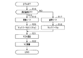
- FIG. 5 shows a procedure of processing executed by the control unit 70. This process is repeatedly executed, for example, at a predetermined control cycle.
- the product of the number of turns of the first voltage V1 and the first coil 50a is larger than the product of the number of turns of the second voltage V2 and the second coil 50b. That is, it is assumed that the electric power is transmitted from the storage battery 10 to the power supply target 11 by this process.
- step S10 it is determined whether the environmental temperature T is equal to or lower than the set temperature.
- step S10 corresponds to the determination unit.
- step S10 If a negative determination is made in step S10, the process proceeds to step S11 assuming that there is no request to increase the calorific value, and the control mode is set to the normal mode. In the normal mode, in the next step S12, the gate voltage Voff when the fifth to eighth switches Q5 to Q8 are off is set to the first off voltage V ⁇ .
- step S10 If an affirmative judgment is made in step S10, the process proceeds to step S13 on the assumption that there is a request to increase the amount of heat generated, and the control mode is set to the heat generation mode.
- the gate voltage Voff when the fifth to eighth switches Q5 to Q8 are off is set to the second off voltage V ⁇ .
- step S15 the command current setting unit 71 sets the command current Iref2.
- step S16 the first to fourth switches Q1 to Q4 are turned on and off, and the fifth to eighth switches Q5 to Q8 are turned off so that the second current I2 is controlled by the command current Iref2.
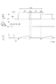
- FIG. 6 shows the transition of the operation state and the like of each switch Q1 to Q8 in the normal mode and the heat generation mode.
- FIG. 6A shows the transition of the operating state of the first to fourth switches Q1 to Q4.
- FIG. 6B shows the transition of the operating state of the 5th to 8th switches Q5 to Q8.
- FIG. 6C shows the transition of the first current I1 and the second current I2.
- FIG. 6D shows the first power P1, the second power P2, and the lost power P1 + P2.
- the first electric power P1 is the time average value of the electric power supplied from the storage battery 10 to the first full bridge circuit 30, and the second electric power P2 is supplied from the second full bridge circuit 40 to the power supply target 11. It is the time average value of the electric power to be generated.
- the first electric power P1 is positive, the storage battery 10 is discharged. Further, when the second electric power P2 is negative, electric power is supplied to the power supply target 11. Therefore, the sum P1 + P2 of the first power P1 and the second power P2 is the lost power.
- FIG. 6E is an enlarged view of the vertical axis of the power loss P1 + P2 in FIG. 6D.
- the scales of the vertical axis in the normal mode and the heat generation mode of FIG. 6 (e) are the same, and are used to compare the magnitudes of the power loss P1 + P2 in the normal mode and the heat generation mode.
- the inter-leg phase ⁇ 1 is set to a value in the range from 0 ° to a predetermined phase so that the second current I2 is feedback-controlled by the command current Iref2.
- the inter-leg phase ⁇ 1 By limiting the inter-leg phase ⁇ 1 to a range from 0 ° to a predetermined phase, it is possible to prevent the inter-leg phase ⁇ 1 from becoming too large and reducing the power that can be transmitted from the storage battery 10 to the power supply target 11.
- the first to fourth periods T1 to T4 appear in one switching cycle Tsw.
- the switching patterns of the normal mode and the heat generation mode are the same.
- the first period T1 the second and third switches Q2 and Q3 are turned on, and the first, fourth, fifth, sixth, seventh and eighth switches Q1, Q4, Q5, Q6 and Q7.
- Q8 is the period during which it is turned off.
- the second period T2 the first, third switches Q1 and Q3 are turned on, and the second, fourth, fifth, sixth, seventh, and eighth switches Q2, Q4, Q5, Q6, and Q7.
- Q8 is the period during which it is turned off.
- the first and fourth switches Q1 and Q4 are turned on, and the second, third, fifth, sixth, seventh, and eighth switches Q2, Q3, Q5, Q6, and Q7. , Q8 is the period during which it is turned off.
- the second and fourth switches Q2 and Q4 are turned on, and the first, third, fifth, sixth, seventh, and eighth switches Q1, Q3, Q5, Q6, and Q7. , Q8 is the period during which it is turned off.
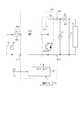
- FIG. 7A shows the current path in the first period T1.
- a current path including the first high potential side terminal CH1, the third switch Q3, the first coil 50a, the second switch Q2, and the first low potential side terminal CL1 is formed.
- the second full bridge circuit 40 a current path including the second low potential side terminal CL2, the sixth switch Q6, the second coil 50b, the seventh switch Q7, and the second high potential side terminal CH2 is formed.
- the 6th switch Q6 and the 7th switch Q7 are turned off, but due to the characteristics of the GaN-HEMT, a reverse conduction current is flowing through the 6th switch Q6 and the 7th switch Q7.
- the first current I1 gradually increases in the positive direction and the second current I2 gradually increases in the negative direction.
- the gate voltage Voff at the time of off is increased to the negative side as compared with the normal mode. Therefore, due to the characteristics of GaN-HEMT, the reverse conduction current of the sixth switch Q6 and the seventh switch Q7 The conduction loss due to is larger than that in the normal mode.
- FIG. 7B shows the current path in the second period T2.
- a current path including the first switch Q1, the third switch Q3, and the first coil 50a is formed.
- the second full bridge circuit 40 the same current path as in the first period T1 is formed.
- the first coil 50a is not connected to the first low potential side terminal CL1, so that the first current I1 is 0 as shown in FIG. 6C.
- the first full bridge circuit 30 an induced voltage is temporarily generated in the first coil 50a so that the potential at the first end is higher than that at the second end.
- an induced voltage is temporarily generated in the second coil 50b so that the potential at the second end is higher than that at the first end. Therefore, the sign of the second current I2 remains negative, and its absolute value gradually decreases. Even in this case, due to the characteristics of GaN-HEMT, the conduction loss due to the reverse conduction current is larger in the heat generation mode than in the normal mode.
- FIG. 7 (c) shows the current path in the third period T3.
- a current path including the first high potential side terminal CH1, the first switch Q1, the first coil 50a, the fourth switch Q4, and the first low potential side terminal CL1 is formed.
- the second full bridge circuit 40 a current path including the second low potential side terminal CL2, the eighth switch Q8, the second coil 50b, the fifth switch Q5, and the second high potential side terminal CH2 is formed.
- the fifth switch Q5 and the eighth switch Q8 are turned off, but due to the characteristics of the GaN-HEMT, a reverse conduction current is passed through the fifth switch Q5 and the eighth switch Q8.
- the first current I1 gradually increases in the positive direction and the second current I2 gradually increases in the negative direction.
- the gate voltage Voff at the time of off is increased to the negative side as compared with the normal mode. Therefore, due to the characteristics of GaN-HEMT, the reverse conduction current of the fifth switch Q5 and the eighth switch Q8 The conduction loss due to is larger than that in the normal mode.
- FIG. 7 (d) shows the current path in the fourth period T4.
- a current path including the second switch Q2, the first coil 50a, and the fourth switch Q4 is formed.
- the second full bridge circuit 40 the same current path as in the third period T3 is formed.
- the first coil 50a is not connected to the first high potential side terminal CH1, so that the first current I1 is 0 as shown in FIG. 6C.
- the first full bridge circuit 30 an induced voltage is temporarily generated in the first coil 50a so that the potential at the second end is higher than that at the first end.
- an induced voltage is temporarily generated in the second coil 50b so that the potential at the first end is higher than that at the second end. Therefore, the sign of the second current I2 remains negative, and its absolute value gradually decreases. Even in this case, due to the characteristics of GaN-HEMT, the conduction loss due to the reverse conduction current is larger in the heat generation mode than in the normal mode.
- FIG. 6C shows the time average value I1ave of the first current I1 and the time average value I2ave of the second current I2 in the first to fourth periods T1 to T4 with broken lines.
- the first current average value I1ave is a positive value
- the second current average value I2ave is a negative value.
- the first power P1 has a positive value
- the second power P2 has a negative value. This indicates that the electric power was transmitted from the storage battery 10 to the power supply target 11 in the first period T1 to the fourth period T4. Since power loss occurs in each of the switches Q1 to Q8 and the like due to this power transmission, the lost power P1 + P2 is a positive value.
- the power loss P1 + P2 in the heat generation mode is larger than the value of the power loss P1 + P2 in the normal mode. This is because in the heat generation mode, the gate voltage Voff at off is increased to the negative side as compared with the normal mode, and therefore, due to the characteristics of GaN-HEMT, the conduction loss due to the reverse conduction current in the 5th to 8th switches Q5 to Q8. This is because
- the fifth to eighth switches Q5 to Q8 are turned off when power is transmitted from the storage battery 10 to the power supply target 11. At this time, a conduction loss is generated as the reverse conduction current flows through the 5th to 8th switches Q5 to Q8, and heat is generated by the conduction loss.
- the power conversion device 20 can be miniaturized.
- the fifth to eighth switches Q5 to Q8 of the present embodiment are composed of GaN-HEMT, when a reverse conduction current flows, the larger the gate voltage Voff at the time of off is on the negative side, the more it occurs. It has the characteristic that the conduction loss is large. Focusing on this characteristic, in the present embodiment, when the heat generation mode is set, the gate voltage Voff when the 5th to 8th switches Q5 to Q8 are off increases to the negative side as compared with the case where the normal mode is set. Will be done. As a result, the conduction loss generated in the fifth to eighth switches Q5 to Q8 when the heat generation mode is set can be made larger than that when the normal mode is set. As a result, the amount of heat generated by the power conversion device 20 can be increased.
- the first to fourth switches Q1 to Q4 are not limited to N-channel MOSFETs, and may be IGBTs.
- the high potential side terminal is the collector and the low potential side terminal is the emitter.
- the first full bridge circuit 30 includes a freewheel diode connected in antiparallel to each of the first to fourth switches Q1 to Q4. In this case, the pair of the switch and the freewheel diode corresponds to the switch portion.
- FIG. 8 is a configuration diagram of this embodiment.
- the power conversion system includes a power conversion device 90.
- the power conversion device 90 includes a third capacitor 91 and a half-bridge circuit 92.
- the half-bridge circuit 92 corresponds to the conversion circuit.
- the half-bridge circuit 92 includes a ninth switch Q9 and a tenth switch Q10.
- the 9th switch Q9 and the 10th switch Q10 are N-channel MOSFETs.
- the first high potential side terminal CH1 is connected to the drain of the ninth switch Q9.
- the drain of the 10th switch Q10 is connected to the source of the 9th switch Q9.
- the first low potential side terminal CL1 and the second end of the first coil 50a are connected to the source of the tenth switch Q10.
- the source of the 9th switch Q9 and the drain of the 10th switch Q10 are connected to the first end of the first coil 50a via the third capacitor 91.
- the control unit 70 alternately turns on the ninth switch Q9 and the tenth switch Q10 constituting the half-bridge circuit 92.
- the duty ratio of the ninth switch Q9 is 0.5.
- the duty ratio is the ratio (Ton / Tsw) of the on-time Ton to the one switching cycle Tsw of the ninth switch Q9.
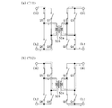
- FIG. 9 shows changes in the operating states of the fifth to tenth switches Q5 to Q10 in the normal mode and the heat generation mode of the present embodiment.
- the solid line in FIG. 9A shows the transition of the operating state of the 9th switch Q9, and the broken line shows the transition of the 10th switch Q10.
- FIG. 9B shows the operating states of the 5th to 8th switches Q5 to Q8.
- FIG. 9C shows the transition of the first current I1 and the second current I2.
- the fifth to eighth periods T5 to T8 appear in one switching cycle Tsw.
- the ninth switch Q9 is turned on, and the fifth, sixth, seventh, eighth, and tenth switches Q5, Q6, Q7, Q8, and Q10 are turned off.
- the 10th switch Q10 is turned on, and the 5th, 6th, 6th, 7th, 8th, and 9th switches Q5, Q6, Q7, Q8, and Q9 are turned off.
- the period. As described above, also in this embodiment, since the fifth to eighth switches Q5 to Q8 constituting the second full bridge circuit 40 are fixed to off, conduction loss due to the reverse conduction current occurs.
- FIG. 10A shows the current path in the fifth period T5.
- a current path including the first high potential side terminal CH1, the ninth switch Q9, the third capacitor 91, the first coil 50a, and the first low potential side terminal CL1 is formed.
- the second full bridge circuit 40 the same current path as in the third period T3 is formed.
- the first current I1 gradually increases in the positive direction in the fifth period T5.
- the second current I2 gradually increases in the negative direction.
- FIG. 10B shows the current path in the sixth period T6.
- a current path including the 10th switch Q10, the 3rd capacitor 91, and the 1st coil 50a is formed in the half-bridge circuit 92.
- the same current path as in the fifth period T5 is formed in the second full bridge circuit 40.
- the first current I1 is 0 as shown in FIG. 9C.
- the half-bridge circuit 92 an induced voltage is temporarily generated in the first coil 50a so that the potential at the second end is higher than that at the first end.
- an induced voltage is temporarily generated in the second coil 50b so that the potential at the first end is higher than that at the second end. Therefore, the sign of the second current I2 remains negative, and its absolute value gradually decreases.
- FIG. 10 (c) shows the current path in the 7th period T7.
- a current in the opposite direction flows in the same current path as in the sixth period T6.
- a current path including the second low potential side terminal CL2, the sixth switch Q6, the second coil 50b, the seventh switch Q7, and the second high potential side terminal CH2 is formed.
- the 1st current I1 is 0 as shown in FIG. 9C. Since the electric charge stored in the third capacitor 91 is discharged to the half-bridge circuit 92, a current flows in the direction opposite to that of the sixth period T6. Therefore, an induced voltage is generated in the second coil 50b so that the potential at the second end is higher than that at the first end. Therefore, the second current I2 gradually increases in the negative direction.
- FIG. 10 (d) shows the current path in the eighth period T8.
- a current path including the first low potential side terminal CL1, the second coil 50b, the third capacitor 91, the ninth switch Q9, and the first high potential side terminal CH1 is formed.
- the second full bridge circuit 40 the same current path as in the seventh period T7 is formed.
- an induced voltage is temporarily generated in the first coil 50a so that the potential at the first end is higher than that at the second end. Therefore, as shown in FIG. 9C, the sign of the first current I1 becomes negative, and its absolute value gradually decreases.
- an induced voltage is temporarily generated in the second coil 50b so that the potential at the second end is higher than that at the first end. Therefore, the sign of the second current I2 remains negative, and its absolute value gradually decreases.
- the half-bridge circuit 92 is used as the configuration of the conversion circuit, the DC voltage supplied from the storage battery 10 can be converted into an alternating voltage. Therefore, using this alternating voltage, a reverse conduction current can be passed through the fifth to eighth switches Q5 to Q8 constituting the second full bridge circuit 40.
- the tenth switch Q10 is not limited to the N-channel MOSFET, but may be an IGBT.
- the second embodiment will be described with reference to the drawings, focusing on the differences from the first embodiment.
- a full bridge circuit is used in the configuration of the power conversion device 20, but this is changed.
- the configuration of the power conversion device is a step-up chopper circuit.
- FIG. 11 shows a configuration diagram of this embodiment.
- the power conversion system includes a storage battery 10, a power supply target 11, a capacitor 12, and a power conversion device 100.
- the power conversion device 100 includes a first high potential side terminal CH1, a first low potential side terminal CL1, a second high potential side terminal CH2, a second low potential side terminal CL2, a half bridge circuit 101, and a reactor 102. ..
- the half-bridge circuit 101 includes an eleventh switch Q11 and a twelfth switch Q12.
- the eleventh switch Q11 is a GaN-HEMT and the twelfth switch Q12 is an IGBT.
- the second high potential side terminal CH2 is connected to the drain of the eleventh switch Q11.
- the collector of the 12th switch Q12 is connected to the source of the 11th switch Q11.
- the first low potential side terminal CL1 and the second low potential side terminal CL2 are connected to the emitter of the twelfth switch Q12.
- the second low potential side terminal CL2 is connected to the second high potential side terminal CH2 via the capacitor 12. Further, the second low potential side terminal CL2 is connected to the second high potential side terminal CH2 via the power supply target 11.
- a diode D as a freewheel diode is connected in antiparallel to the 12th switch Q12.
- the twelfth switch Q12 is not limited to the IGBT, and an N-channel MOSFET may be used. In this case, the diode D may not be provided.
- the first end of the reactor 102 is connected to the first high potential side terminal CH1.
- the second end of the reactor 102 is connected to the source of the 11th switch Q11 and the collector of the 12th switch Q12.
- the positive electrode terminal of the storage battery 10 is connected to the first high potential side terminal CH1, and the first low potential side terminal CL1 is connected to the negative electrode terminal of the storage battery 10.
- the power conversion system includes a first current sensor 60, a first voltage sensor 61, a second current sensor 62, a second voltage sensor 63, and a temperature sensor 64.
- the detection target of these sensors is the same as that of the first embodiment.
- the control unit 70 outputs a drive signal to the gates of the 11th switch Q11 and the 12th switch Q12 based on the detected values I1, V1, I2, V2, T, and turns the 11th switch Q11 and the 12th switch Q12 on and off.
- the definition of the code of the first current I1 is the same as that of the first embodiment, but the second current I2 is a case where a current flows from the second high potential side terminal CH2 in the direction of the power supply target 11. Is positive, and the case where current flows in the opposite direction is negative.
- FIG. 12 is a control block diagram implemented by the control unit 70 in this embodiment.
- the control unit 70 includes a voltage controller 82.
- the voltage controller 82 includes a voltage deviation calculation unit 83, a feedback control unit 77, and a duty ratio calculation unit 84.
- the voltage deviation calculation unit 83 calculates the voltage deviation ⁇ V2 by subtracting the second voltage V2, which is the detection voltage of the second voltage sensor 63, from the command voltage V2 *.
- the feedback control unit 77 calculates the duty ratio of the 12th switch Q12 as an operation amount for feeding back the calculated voltage deviation ⁇ V2 to 0.
- the duty ratio calculation unit 84 adds the feedforward term (V2 * -V1) / V2 * to the duty ratio calculated by the feedback control unit 77 to obtain the final duty ratio of the 12th switch Q12.
- the duty ratio of the 12th switch Q12 is output to the PWM generation unit 79.
- the PWM generation unit 79 generates drive signals for the 11th switch Q11 and the 12th switch Q12 and outputs them to the gate voltage correction unit 85.
- the eleventh switch Q11 is turned off.
- the twelfth switch Q12 is turned on and off based on the duty ratio of the twelfth switch Q12.
- the gate voltage correction unit 85 corrects the gate voltage Voff when the 11th switch Q11 is off, based on the command received from the gate voltage setting unit 81. After that, the gate voltage correction unit 85 outputs the drive signal to the 11th switch Q11 and the 12th switch Q12.
- the gate voltage setting unit 81 sets the gate voltage Voff when the eleventh switch Q11 is off, as in the first embodiment.
- FIG. 13 shows a procedure of processing executed by the control unit 70. This process is repeatedly executed, for example, at a predetermined control cycle.
- FIG. 13 the same processing as that shown in FIG. 5 above is designated by the same reference numerals for convenience.
- step S10 If a negative determination is made in step S10, the process proceeds to step S17 assuming that there is no request to increase the calorific value, and the control mode is set to the normal mode. In the normal mode, in the next step S18, the gate voltage Voff when the eleventh switch Q11 is off is set to the first off voltage V ⁇ .
- step S10 If an affirmative judgment is made in step S10, the process proceeds to step S19 on the assumption that there is a request to increase the amount of heat generated, and the control mode is set to the heat generation mode.
- the gate voltage Voff when the 11th switch Q11 is off is set to the second off voltage V ⁇ .
- the second off voltage V ⁇ is a value increased to the negative side of the first off voltage V ⁇ .
- step S21 the value of the command voltage V2 * is set.
- step S22 the eleventh switch Q11 is turned off, and the duty ratio of the twelfth switch Q12 is controlled so that the second voltage V2 is controlled by the command voltage V2 *.
- FIG. 14 shows changes in the operating states of the 11th switch Q11 and the 12th switch Q12 in the normal mode and the heat generation mode.
- the solid line in FIG. 14A shows the transition of the operating state of the 11th switch Q11, and the broken line shows the transition of the operating state of the 12th switch Q12.
- FIG. 14B shows a first voltage V1 and a second voltage V2.
- FIG. 14C shows the transition of the first current I1 and the second current I2.
- FIG. 14D shows the first power P1, the second power P2, and the lost power P1-P2.
- the case where the second electric power P2 is supplied from the electric power conversion device 100 to the power supply target 11 is positive. Therefore, the value obtained by subtracting the second power P2 from the first power P1 is the lost power P1-P2.
- the power loss P1-P2 in the heat generation mode is larger than the power loss P1-P2 in the normal mode. This is because, also in the present embodiment, in the heat generation mode, the gate voltage Voff at the time of off is increased to the negative side as compared with the normal mode. Therefore, due to the characteristics of GaN-HEMT, the conduction due to the reverse conduction current in the 11th switch Q11 This is because the loss becomes large.
- the gate voltage setting unit 81 controls the gate voltage Voff when the fifth to eighth switches Q5 to Q8 are off based on the environmental temperature T.
- FIG. 15 shows a voltage control method implemented by the gate voltage setting unit 81.
- the upper limit temperature TL is a temperature set from the heat resistance of the element to be heated, and is set to, for example, the allowable upper limit temperature of the element to be heated.
- the gate voltage setting unit 81 sets the gate voltage Voff when the fifth to eighth switches Q5 to Q8 are off. Set to a value according to the temperature T. Specifically, when the environmental temperature T exceeds the limit start temperature TC, the gate voltage setting unit 81 sets the gate voltage Voff when the fifth to eighth switches Q5 to Q8 are off as the environmental temperature T approaches the upper limit temperature TL.
- the gate voltage setting unit 81 sets the gate voltage Voff when the fifth to eighth switches Q5 to Q8 are off to the first off voltage V ⁇ .
- the gate voltage Voff when the fifth to eighth switches Q5 to Q8 set in this way are off is output to the gate voltage correction unit 80.
- the gate voltage Voff at the time of off is set to the first off voltage V ⁇ .
- the off gate voltage Voff is set to the second off voltage V ⁇ .
- the gate voltage Voff of the 5th to 8th switches Q5 to Q8 is gradually reduced based on the environmental temperature T to reduce heat generation due to the reverse conduction current. be able to. As a result, it is possible to prevent the environmental temperature T from exceeding the upper limit temperature TL.
- FIG. 16 is a control block diagram implemented by the gate voltage setting unit 81 in the heat generation mode of the present embodiment.
- the gate voltage setting unit 81 includes a temperature controller 86.
- the temperature controller 86 includes a temperature deviation calculation unit 87, a feedback control unit 88, and a limiter 89.
- the temperature deviation calculation unit 87 calculates the temperature deviation ⁇ T by subtracting the environmental temperature T from the target temperature T *.
- the target temperature T * corresponds to the command temperature.
- the feedback control unit 88 calculates the gate voltage Voff when the fifth to eighth switches Q5 to Q8 are off as the operation amount for feeding back the calculated temperature deviation ⁇ T to 0. For example, when the environmental temperature T is raised, the gate voltage Voff at the time of off is increased to the negative side. On the other hand, when the environmental temperature T is lowered, the absolute value of the gate voltage Voff at the time of off is reduced.
- proportional integral control is used as this feedback control.
- the feedback control used in the feedback control unit 88 is not limited to the proportional integral control, and may be, for example, the proportional integral differential control.
- the upper limit value or lower limit value of the gate voltage Voff when the fifth to eighth switches Q5 to Q8 calculated by the feedback control unit 88 is off is limited by the limiter 89, and is output to the gate voltage correction unit 80.
- the upper limit value is the first off voltage V ⁇
- the lower limit value is the voltage determined from the characteristics of the fifth to eighth switches Q5 to Q8.
- the environmental temperature T can be controlled to the target temperature T *.
- control unit 70 temporarily switches the gate voltage Voff when the fifth switch Q5 and the sixth switch Q6 are off from the second off voltage V ⁇ to the first off voltage V ⁇ .
- FIG. 17 shows the transition of the operating state and the like of the switches Q1 to Q8 in each of the case where the gate voltage Voff at the time of off is fixed and the case where the gate voltage Voff at the time of off is temporarily switched.
- FIG. 17A shows the transition of the operating state of the first switch Q1 and the fourth switch Q4. The operating state in which the operating states of the first switch Q1 and the fourth switch Q4 are reversed becomes the operating state of the second switch Q2 and the third switch Q3.
- FIG. 17B shows the transition of the operating state of the fifth to eighth switches Q5 to Q8. Also in this embodiment, the fifth to eighth switches Q5 to Q8 are turned off.
- FIG. 17C shows the transition of the gate voltage Voff when the fifth switch Q5 and the sixth switch Q6 are off.
- FIG. 17D shows the transition of the first current I1 and the second current I2.
- the control unit 70 fixes the gate voltage Voff when the fifth switch Q5 and the sixth switch Q6 are off to the second off voltage V ⁇ .
- the control unit 70 temporarily switches the gate voltage Voff at the time of off from the second off voltage V ⁇ to the first off voltage V ⁇ .
- the control unit 70 controls the gate voltage Voff when the sixth switch Q6 is off to the first off voltage V ⁇ .
- the operating states of the switches Q1 to Q8 in the ninth period T9 are the same as those in the first period T1.
- the current path of the 9th period T9 is the same as that of the 1st period T1.
- the gate voltage Voff when the sixth switch Q6 is off is switched from the second off voltage V ⁇ to the first off voltage V ⁇ , so that the voltage drop amount of the sixth switch Q6 becomes smaller.
- the conduction loss of the sixth switch Q6 becomes smaller. Therefore, as shown in FIG. 17D, the second current I2 increases to the negative side in the case of Voff switching as compared with the case of Voff fixing. The speed will increase.
- the operating states of the switches Q1 to Q8 in the 10th period T10 are the same as those in the 3rd period T3.
- the current path of the 10th period T10 is the same as that of the 3rd period T3.
- the gate voltage Voff when the fifth switch Q5 is off is switched from the second off voltage V ⁇ to the first off voltage V ⁇ , so that the voltage drop amount of the fifth switch Q5 becomes smaller.
- the conduction loss of the fifth switch Q5 becomes small, as shown in FIG. 17D, when the Voff is switched, the second current I2 is moved to the negative side as compared with the case where the Voff is fixed. Increases the rate of increase.
- the control unit 70 sets the gate voltage Voff at the time of turning off the switch through which the reverse conduction current is flowing to the first off voltage within the period when the fifth to eighth switches Q5 to Q8 are turned off.
- a period for temporarily switching to V ⁇ is provided.
- the reverse conduction current is increased during this period, so that the gate voltage Voff at the time of off is returned to the second off voltage V ⁇ .
- the reverse conduction current can be passed through the 5th to 8th switches Q5 to Q8. As a result, the conduction loss due to the reverse conduction current can be increased, so that the amount of heat generated by the power conversion device 20 can be increased.
- the value for temporarily switching the gate voltage Voff at the time of off is set to the first off voltage V ⁇ , but this value is not limited to the first off voltage V ⁇ , and the magnitude of the reverse conduction current is adjusted. Therefore, it may be adjusted in a direction in which the conduction loss is reduced.
- the time width for temporarily switching the gate voltage Voff when off is increased, the reverse conduction current increases, but the amount of heat generated by the reverse conduction current decreases. Therefore, if the time width for temporarily switching the gate voltage Voff at the time of off is increased, the calorific value per switching cycle reaches the maximum value and then starts to decrease.
- a desired calorific value can be obtained as the time width for temporarily switching the gate voltage Voff at the time of off. It may be set to the time width.
- the fifth embodiment will be described with reference to the drawings, focusing on the differences from the first embodiment.
- the switching pattern in the heat generation mode is changed.
- the fifth to eighth switches Q5 to Q8 are turned off in the heat generation mode, but in the present embodiment, the fifth to eighth switches Q5 to Q8 are turned on and off.
- FIG. 18 shows the transition of the operating state and the like of the switches Q1 to Q8 in the heat generation mode of the present embodiment.
- the solid line in FIG. 18A shows the transition of the operating state of the first switch Q1.
- the operation state in which the operation state of the first switch Q1 is reversed becomes the operation state of the second switch Q2.
- the broken line in FIG. 18A shows the operating state of the fourth switch Q4.
- the operation state in which the operation state of the fourth switch Q4 is reversed becomes the operation state of the third switch Q3.
- the solid line in FIG. 18B shows the transition of the operating state of the fifth switch Q5.
- the operation state in which the operation state of the fifth switch Q5 is reversed becomes the operation state of the sixth switch Q6.
- the broken line in FIG. 18B shows the transition of the operating state of the eighth switch Q8.
- the operation state in which the operation state of the eighth switch Q8 is reversed becomes the operation state of the seventh switch Q7.
- the transmitted power between the first full bridge circuit 30 and the second full bridge circuit 40 is adjusted by controlling the intercircuit phase ⁇ 21.
- the inter-circuit phase ⁇ 21 is the phase difference between the on-switching timing of the fourth switch Q4 and the on-switching timing of the eighth switch Q8.
- FIG. 18C shows the transition of the gate voltage of the 5th switch Q5 and the 8th switch Q8.
- Von1 indicates the on-time gate voltage in the normal mode
- Von2 indicates the on-time gate voltage in the heat generation mode.
- the gate voltage Von2 at the time of turning on in the heat generation mode is reduced as compared with the gate voltage Von1 at the time of turning on in the normal mode.
- Voff1 indicates the gate voltage at the time of off in the normal mode
- Voff2 indicates the gate voltage at the time of off in the heat generation mode.
- the gate voltage Voff2 at the time of off in the heat generation mode is increased to the negative side as compared with the gate voltage Voff1 at the time of off in the normal mode. For example, in the eleventh period T11 shown in FIG.
- the gate voltage when the fifth switch Q5 and the eighth switch Q8 are on is set to Von2. Further, in the 12th period T12, the gate voltage when the fifth switch Q5 is on is set to Von2, and the gate voltage when the eighth switch Q8 is off is set to Voff2.
- the 1st, 4th, 5th, and 8th switches Q1, Q4, Q5, and Q8 are turned on, and the 2nd, 3rd, 6th, and 7th switches Q2, Q3, and Q6. This is the period during which Q7 is turned off.
- the current path of the 11th period T11 is the same as that of the 3rd period T3.
- the fifth switch Q5 and the eighth switch Q8 are turned on. Therefore, the control unit 70 sets the gate voltage at the time of turning on the fifth switch Q5 and the eighth switch Q8 through which the reverse conduction current flows to Von2, which is smaller than the gate voltage Von1 at the time of turning on in the normal mode.
- the conduction loss at the time of conduction can be increased.
- the second, third, fifth, and seventh switches Q2, Q3, Q5, and Q7 are turned on, and the first, fourth, sixth, and eighth switches Q1, Q4, and Q6. This is the period during which Q8 is turned off.
- FIG. 19B shows the current path of the 12th period T12.
- a circuit including the second coil 50b, the seventh switch Q7, and the fifth switch Q5 is formed.
- the control unit 70 sets the gate voltage at the time of turning on the fifth switch Q5 through which the forward conducting current flows to Von2, which is smaller than the gate voltage Von1 at the time of turning on in the normal mode. The conduction loss can be increased.
- FIG. 20 shows the characteristics of the forward conduction current amount and the voltage drop amount when the gate voltage when the fifth to eighth switches Q5 to Q8 are turned on is reduced.
- the arrows in FIG. 20 indicate that the gate voltage when on is reduced. It can be seen that when the gate voltage at the time of ON is reduced, the amount of voltage drop for the same amount of forward conduction current increases.
- the present embodiment by reducing the gate voltage at the time of turning on in the heat generation mode as compared with the normal mode, the voltage drop amount of the fifth to eighth switches Q5 to Q8 is increased, and the conduction loss is increased. be able to.
- the fifth to eighth switches Q5 It is also possible to reduce the stress applied to Q8. As a result, deterioration of the fifth to eighth switches Q5 to Q8 can be suppressed.
- FIG. 21 shows a control block diagram carried out by the control unit 70 in the normal mode.
- the same components as those in FIG. 2 above are designated by the same reference numerals for convenience.
- the feedback control unit 77 calculates the inter-circuit phase ⁇ 21 as an operation amount for feeding back the current deviation ⁇ I2 to 0.
- the inter-circuit phase ⁇ 21 is limited to a range from 0 ° to a predetermined phase, and in that range, the larger the value, the larger the transmitted power from the storage battery 10 to the power supply target 11.
- the PWM generation unit 79 generates drive signals for the switches Q1 to Q8 based on the inter-circuit phase ⁇ 21.
- FIG. 22 shows the transition of the operating state of each switch Q1 to Q8 in the normal mode.
- the solid line in FIG. 22A shows the transition of the operating state of the first switch Q1.
- the operation state in which the operation state of the first switch Q1 is reversed becomes the operation state of the second switch Q2.
- the broken line in FIG. 22A shows the transition of the operating state of the third switch Q3.
- the operation state in which the operation state of the third switch Q3 is reversed becomes the operation state of the fourth switch Q4.
- the solid line in FIG. 22B shows the transition of the operating state of the fifth switch Q5.
- the operation state in which the operation state of the fifth switch Q5 is reversed becomes the operation state of the sixth switch Q6.
- the broken line in FIG. 22B shows the transition of the operating state of the seventh switch Q7.
- the operation state in which the operation state of the seventh switch Q7 is reversed becomes the operation state of the eighth switch Q8.
- the phase difference between the on-switching timing of the first switch Q1 and the on-switching timing of the fifth switch Q5 is defined as the inter-circuit phase ⁇ 21.
- FIG. 23 shows a configuration diagram of this embodiment.
- the power conversion device 20 includes a heat transfer unit 110.
- the heat transfer unit 110 has each switch Q1 to Q8, a transformer 50, and a power supply target 11 as heat exchange target elements, and is configured to be able to absorb heat generated by the heat exchange target elements.
- the heat transfer unit 110 transfers the absorbed heat to the element to be heated, and raises the temperature of the element to be heated.
- the element to be heated is, for example, the power supply target 11.
- the heat transfer unit 110 includes, for example, a circulation path in which cooling water circulates between the heat exchange target element and the temperature rise target element, and raises the temperature of the temperature rise target element through the cooling water. May be good.
- the heat transfer unit 110 may use, for example, a gas (air) as the cooling fluid.
- the heat transfer unit 110 may be, for example, a constituent member such as a heat sink that comes into contact with the heat exchange target element and the temperature rise target element without using a cooling fluid.
- the heat generated by the power conversion can be recovered and transferred to the element to be heated, so that the temperature of the element to be heated can be efficiently increased.
- the circuit configuration of the power conversion device 20 of the first embodiment is used, but the modified example 2 of the first embodiment is used.
- the same effect can be obtained by using the circuit configuration of the power conversion device 90 shown in 1.
- the controls and methods thereof described in the present disclosure are provided by a dedicated computer provided by configuring a processor and memory programmed to perform one or more functions embodied by a computer program. It may be realized. Alternatively, the controls and methods thereof described in the present disclosure may be implemented by a dedicated computer provided by configuring the processor with one or more dedicated hardware logic circuits. Alternatively, the control unit and method thereof described in the present disclosure may be a combination of a processor and memory programmed to perform one or more functions and a processor composed of one or more hardware logic circuits. It may be realized by one or more dedicated computers configured. Further, the computer program may be stored in a computer-readable non-transitional tangible recording medium as an instruction executed by the computer.
Landscapes
- Engineering & Computer Science (AREA)
- Power Engineering (AREA)
- Transportation (AREA)
- Mechanical Engineering (AREA)
- Inverter Devices (AREA)
- Dc-Dc Converters (AREA)
- Electric Propulsion And Braking For Vehicles (AREA)
Priority Applications (3)
| Application Number | Priority Date | Filing Date | Title |
|---|---|---|---|
| CN202080076480.3A CN114631255B (zh) | 2019-10-30 | 2020-10-28 | 电力转换装置 |
| DE112020005352.0T DE112020005352T5 (de) | 2019-10-30 | 2020-10-28 | Leistungsumwandlungsvorrichtung |
| US17/730,417 US12015351B2 (en) | 2019-10-30 | 2022-04-27 | Power conversion apparatus |
Applications Claiming Priority (2)
| Application Number | Priority Date | Filing Date | Title |
|---|---|---|---|
| JP2019-197371 | 2019-10-30 | ||
| JP2019197371A JP7075385B2 (ja) | 2019-10-30 | 2019-10-30 | 電力変換装置 |
Related Child Applications (1)
| Application Number | Title | Priority Date | Filing Date |
|---|---|---|---|
| US17/730,417 Continuation US12015351B2 (en) | 2019-10-30 | 2022-04-27 | Power conversion apparatus |
Publications (1)
| Publication Number | Publication Date |
|---|---|
| WO2021085515A1 true WO2021085515A1 (ja) | 2021-05-06 |
Family
ID=75713845
Family Applications (1)
| Application Number | Title | Priority Date | Filing Date |
|---|---|---|---|
| PCT/JP2020/040536 Ceased WO2021085515A1 (ja) | 2019-10-30 | 2020-10-28 | 電力変換装置 |
Country Status (5)
| Country | Link |
|---|---|
| US (1) | US12015351B2 (https=) |
| JP (1) | JP7075385B2 (https=) |
| CN (1) | CN114631255B (https=) |
| DE (1) | DE112020005352T5 (https=) |
| WO (1) | WO2021085515A1 (https=) |
Families Citing this family (2)
| Publication number | Priority date | Publication date | Assignee | Title |
|---|---|---|---|---|
| JP7719659B2 (ja) * | 2021-07-30 | 2025-08-06 | 株式会社Soken | 電力変換装置、プログラム |
| JP7712817B2 (ja) * | 2021-07-30 | 2025-07-24 | 株式会社Soken | 電力変換装置、プログラム |
Citations (5)
| Publication number | Priority date | Publication date | Assignee | Title |
|---|---|---|---|---|
| JP2008029050A (ja) * | 2006-07-18 | 2008-02-07 | Toyota Motor Corp | 電源システムおよびそれを備えた車両、蓄電装置の昇温制御方法、ならびに蓄電装置の昇温制御をコンピュータに実行させるためのプログラムを記録したコンピュータ読取可能な記録媒体 |
| JP2014146589A (ja) * | 2013-01-28 | 2014-08-14 | Samsung Sdi Co Ltd | バッテリ温度制御システムおよびその制御方法 |
| JP2016092884A (ja) * | 2014-10-30 | 2016-05-23 | 株式会社デンソー | 半導体素子の駆動回路及び半導体素子の駆動システム |
| JP2019004544A (ja) * | 2017-06-12 | 2019-01-10 | 株式会社デンソー | 制御システム |
| WO2019097926A1 (ja) * | 2017-11-16 | 2019-05-23 | 株式会社村田製作所 | 蓄電モジュールおよび電源システム |
Family Cites Families (7)
| Publication number | Priority date | Publication date | Assignee | Title |
|---|---|---|---|---|
| JP3451141B2 (ja) | 1994-11-14 | 2003-09-29 | 本田技研工業株式会社 | バッテリ温度調節装置 |
| JP4396287B2 (ja) * | 2004-01-22 | 2010-01-13 | 富士電機ホールディングス株式会社 | 電力制御装置 |
| JP6072645B2 (ja) * | 2013-08-08 | 2017-02-01 | 株式会社日立製作所 | 電力変換装置 |
| JP5744144B2 (ja) * | 2013-09-26 | 2015-07-01 | 三菱電機株式会社 | 誘導性負荷の給電制御装置 |
| US10017030B2 (en) * | 2016-09-27 | 2018-07-10 | Hanon Systems | Efficient transfer of heat to passenger cabin |
| US11368031B2 (en) * | 2017-11-08 | 2022-06-21 | Eaton Intelligent Power Limited | Power distribution and circuit protection for a mobile application having a high efficiency inverter |
| JP7087650B2 (ja) | 2018-05-09 | 2022-06-21 | 株式会社島津製作所 | データ検索装置、データ蓄積システムおよびデータ検索方法 |
-
2019
- 2019-10-30 JP JP2019197371A patent/JP7075385B2/ja active Active
-
2020
- 2020-10-28 DE DE112020005352.0T patent/DE112020005352T5/de active Pending
- 2020-10-28 WO PCT/JP2020/040536 patent/WO2021085515A1/ja not_active Ceased
- 2020-10-28 CN CN202080076480.3A patent/CN114631255B/zh active Active
-
2022
- 2022-04-27 US US17/730,417 patent/US12015351B2/en active Active
Patent Citations (5)
| Publication number | Priority date | Publication date | Assignee | Title |
|---|---|---|---|---|
| JP2008029050A (ja) * | 2006-07-18 | 2008-02-07 | Toyota Motor Corp | 電源システムおよびそれを備えた車両、蓄電装置の昇温制御方法、ならびに蓄電装置の昇温制御をコンピュータに実行させるためのプログラムを記録したコンピュータ読取可能な記録媒体 |
| JP2014146589A (ja) * | 2013-01-28 | 2014-08-14 | Samsung Sdi Co Ltd | バッテリ温度制御システムおよびその制御方法 |
| JP2016092884A (ja) * | 2014-10-30 | 2016-05-23 | 株式会社デンソー | 半導体素子の駆動回路及び半導体素子の駆動システム |
| JP2019004544A (ja) * | 2017-06-12 | 2019-01-10 | 株式会社デンソー | 制御システム |
| WO2019097926A1 (ja) * | 2017-11-16 | 2019-05-23 | 株式会社村田製作所 | 蓄電モジュールおよび電源システム |
Also Published As
| Publication number | Publication date |
|---|---|
| CN114631255B (zh) | 2026-02-06 |
| DE112020005352T5 (de) | 2022-08-04 |
| JP7075385B2 (ja) | 2022-05-25 |
| CN114631255A (zh) | 2022-06-14 |
| JP2021072696A (ja) | 2021-05-06 |
| US12015351B2 (en) | 2024-06-18 |
| US20220255445A1 (en) | 2022-08-11 |
Similar Documents
| Publication | Publication Date | Title |
|---|---|---|
| CN104410252B (zh) | 源极驱动电路及其控制方法 | |
| CN105763032B (zh) | 电子装置及其控制方法 | |
| JP2021090264A (ja) | スイッチング回路のゲート駆動回路および制御回路、スイッチング電源 | |
| TWI496403B (zh) | 電壓轉換控制器及電壓轉換電路 | |
| CN114616117B (zh) | 电力转换装置 | |
| CN114097170B (zh) | 电源系统 | |
| JP2001078435A (ja) | 電流制御型半導体スイッチング素子を使用した電力変換装置におけるスイッチング素子の駆動装置 | |
| CN110994982B (zh) | 一种软开关方式的buck变换器及其控制方法 | |
| JP7075385B2 (ja) | 電力変換装置 | |
| US11764696B2 (en) | Direct-current voltage converter for bidirectional electrical power transmission from a primary side to a secondary side of the direct-current voltage converter or vice versa | |
| TW201916567A (zh) | 絕緣型雙向dc/dc變換裝置及絕緣型雙向dc/dc變換電路的控制方法 | |
| KR20070110997A (ko) | 스위치 구동장치, 이를 사용하는 하프 브릿지 컨버터 및 그구동방법 | |
| WO2019142704A1 (ja) | 車載用のdcdcコンバータ | |
| JP7320783B2 (ja) | 電力変換装置 | |
| TWM453302U (zh) | 切換式電源供應器及其控制電路 | |
| US10312826B2 (en) | Power conversion apparatus | |
| US20260039212A1 (en) | High-side device control in phase shift full bridge dc/dc converter | |
| CN223194604U (zh) | 驱动电路及电压转换器 | |
| JP7712817B2 (ja) | 電力変換装置、プログラム | |
| EP4586477A1 (en) | Soft-switch resonant converter and control method thereof | |
| JP2014222969A (ja) | 電圧変換装置 | |
| CN118353274A (zh) | 电力转换装置和电力转换装置的控制方法 | |
| WO2025109887A1 (ja) | 整流回路、整流回路の制御方法 | |
| JP2026060843A (ja) | 駆動回路、電圧変換器及びその制御方法 | |
| CN121907009A (zh) | 一种全效同步整流系统及控制方法 |
Legal Events
| Date | Code | Title | Description |
|---|---|---|---|
| 121 | Ep: the epo has been informed by wipo that ep was designated in this application |
Ref document number: 20881207 Country of ref document: EP Kind code of ref document: A1 |
|
| 122 | Ep: pct application non-entry in european phase |
Ref document number: 20881207 Country of ref document: EP Kind code of ref document: A1 |