WO2021085515A1 - 電力変換装置 - Google Patents
電力変換装置 Download PDFInfo
- Publication number
- WO2021085515A1 WO2021085515A1 PCT/JP2020/040536 JP2020040536W WO2021085515A1 WO 2021085515 A1 WO2021085515 A1 WO 2021085515A1 JP 2020040536 W JP2020040536 W JP 2020040536W WO 2021085515 A1 WO2021085515 A1 WO 2021085515A1
- Authority
- WO
- WIPO (PCT)
- Prior art keywords
- switch
- gate voltage
- voltage
- power
- temperature
- Prior art date
Links
Images


Classifications
-
- H—ELECTRICITY
- H02—GENERATION; CONVERSION OR DISTRIBUTION OF ELECTRIC POWER
- H02M—APPARATUS FOR CONVERSION BETWEEN AC AND AC, BETWEEN AC AND DC, OR BETWEEN DC AND DC, AND FOR USE WITH MAINS OR SIMILAR POWER SUPPLY SYSTEMS; CONVERSION OF DC OR AC INPUT POWER INTO SURGE OUTPUT POWER; CONTROL OR REGULATION THEREOF
- H02M1/00—Details of apparatus for conversion
- H02M1/0003—Details of control, feedback or regulation circuits
-
- H—ELECTRICITY
- H02—GENERATION; CONVERSION OR DISTRIBUTION OF ELECTRIC POWER
- H02M—APPARATUS FOR CONVERSION BETWEEN AC AND AC, BETWEEN AC AND DC, OR BETWEEN DC AND DC, AND FOR USE WITH MAINS OR SIMILAR POWER SUPPLY SYSTEMS; CONVERSION OF DC OR AC INPUT POWER INTO SURGE OUTPUT POWER; CONTROL OR REGULATION THEREOF
- H02M3/00—Conversion of dc power input into dc power output
- H02M3/22—Conversion of dc power input into dc power output with intermediate conversion into ac
- H02M3/24—Conversion of dc power input into dc power output with intermediate conversion into ac by static converters
- H02M3/28—Conversion of dc power input into dc power output with intermediate conversion into ac by static converters using discharge tubes with control electrode or semiconductor devices with control electrode to produce the intermediate ac
- H02M3/325—Conversion of dc power input into dc power output with intermediate conversion into ac by static converters using discharge tubes with control electrode or semiconductor devices with control electrode to produce the intermediate ac using devices of a triode or a transistor type requiring continuous application of a control signal
- H02M3/335—Conversion of dc power input into dc power output with intermediate conversion into ac by static converters using discharge tubes with control electrode or semiconductor devices with control electrode to produce the intermediate ac using devices of a triode or a transistor type requiring continuous application of a control signal using semiconductor devices only
- H02M3/33569—Conversion of dc power input into dc power output with intermediate conversion into ac by static converters using discharge tubes with control electrode or semiconductor devices with control electrode to produce the intermediate ac using devices of a triode or a transistor type requiring continuous application of a control signal using semiconductor devices only having several active switching elements
- H02M3/33576—Conversion of dc power input into dc power output with intermediate conversion into ac by static converters using discharge tubes with control electrode or semiconductor devices with control electrode to produce the intermediate ac using devices of a triode or a transistor type requiring continuous application of a control signal using semiconductor devices only having several active switching elements having at least one active switching element at the secondary side of an isolation transformer
-
- B—PERFORMING OPERATIONS; TRANSPORTING
- B60—VEHICLES IN GENERAL
- B60L—PROPULSION OF ELECTRICALLY-PROPELLED VEHICLES; SUPPLYING ELECTRIC POWER FOR AUXILIARY EQUIPMENT OF ELECTRICALLY-PROPELLED VEHICLES; ELECTRODYNAMIC BRAKE SYSTEMS FOR VEHICLES IN GENERAL; MAGNETIC SUSPENSION OR LEVITATION FOR VEHICLES; MONITORING OPERATING VARIABLES OF ELECTRICALLY-PROPELLED VEHICLES; ELECTRIC SAFETY DEVICES FOR ELECTRICALLY-PROPELLED VEHICLES
- B60L1/00—Supplying electric power to auxiliary equipment of vehicles
- B60L1/02—Supplying electric power to auxiliary equipment of vehicles to electric heating circuits
- B60L1/04—Supplying electric power to auxiliary equipment of vehicles to electric heating circuits fed by the power supply line
-
- H—ELECTRICITY
- H02—GENERATION; CONVERSION OR DISTRIBUTION OF ELECTRIC POWER
- H02J—CIRCUIT ARRANGEMENTS OR SYSTEMS FOR SUPPLYING OR DISTRIBUTING ELECTRIC POWER; SYSTEMS FOR STORING ELECTRIC ENERGY
- H02J7/00—Circuit arrangements for charging or depolarising batteries or for supplying loads from batteries
- H02J7/0063—Circuit arrangements for charging or depolarising batteries or for supplying loads from batteries with circuits adapted for supplying loads from the battery
-
- H—ELECTRICITY
- H02—GENERATION; CONVERSION OR DISTRIBUTION OF ELECTRIC POWER
- H02M—APPARATUS FOR CONVERSION BETWEEN AC AND AC, BETWEEN AC AND DC, OR BETWEEN DC AND DC, AND FOR USE WITH MAINS OR SIMILAR POWER SUPPLY SYSTEMS; CONVERSION OF DC OR AC INPUT POWER INTO SURGE OUTPUT POWER; CONTROL OR REGULATION THEREOF
- H02M1/00—Details of apparatus for conversion
- H02M1/08—Circuits specially adapted for the generation of control voltages for semiconductor devices incorporated in static converters
-
- H—ELECTRICITY
- H02—GENERATION; CONVERSION OR DISTRIBUTION OF ELECTRIC POWER
- H02M—APPARATUS FOR CONVERSION BETWEEN AC AND AC, BETWEEN AC AND DC, OR BETWEEN DC AND DC, AND FOR USE WITH MAINS OR SIMILAR POWER SUPPLY SYSTEMS; CONVERSION OF DC OR AC INPUT POWER INTO SURGE OUTPUT POWER; CONTROL OR REGULATION THEREOF
- H02M3/00—Conversion of dc power input into dc power output
- H02M3/02—Conversion of dc power input into dc power output without intermediate conversion into ac
- H02M3/04—Conversion of dc power input into dc power output without intermediate conversion into ac by static converters
- H02M3/10—Conversion of dc power input into dc power output without intermediate conversion into ac by static converters using discharge tubes with control electrode or semiconductor devices with control electrode
- H02M3/145—Conversion of dc power input into dc power output without intermediate conversion into ac by static converters using discharge tubes with control electrode or semiconductor devices with control electrode using devices of a triode or transistor type requiring continuous application of a control signal
- H02M3/155—Conversion of dc power input into dc power output without intermediate conversion into ac by static converters using discharge tubes with control electrode or semiconductor devices with control electrode using devices of a triode or transistor type requiring continuous application of a control signal using semiconductor devices only
- H02M3/156—Conversion of dc power input into dc power output without intermediate conversion into ac by static converters using discharge tubes with control electrode or semiconductor devices with control electrode using devices of a triode or transistor type requiring continuous application of a control signal using semiconductor devices only with automatic control of output voltage or current, e.g. switching regulators
- H02M3/158—Conversion of dc power input into dc power output without intermediate conversion into ac by static converters using discharge tubes with control electrode or semiconductor devices with control electrode using devices of a triode or transistor type requiring continuous application of a control signal using semiconductor devices only with automatic control of output voltage or current, e.g. switching regulators including plural semiconductor devices as final control devices for a single load
- H02M3/1588—Conversion of dc power input into dc power output without intermediate conversion into ac by static converters using discharge tubes with control electrode or semiconductor devices with control electrode using devices of a triode or transistor type requiring continuous application of a control signal using semiconductor devices only with automatic control of output voltage or current, e.g. switching regulators including plural semiconductor devices as final control devices for a single load comprising at least one synchronous rectifier element
-
- H—ELECTRICITY
- H02—GENERATION; CONVERSION OR DISTRIBUTION OF ELECTRIC POWER
- H02M—APPARATUS FOR CONVERSION BETWEEN AC AND AC, BETWEEN AC AND DC, OR BETWEEN DC AND DC, AND FOR USE WITH MAINS OR SIMILAR POWER SUPPLY SYSTEMS; CONVERSION OF DC OR AC INPUT POWER INTO SURGE OUTPUT POWER; CONTROL OR REGULATION THEREOF
- H02M3/00—Conversion of dc power input into dc power output
- H02M3/22—Conversion of dc power input into dc power output with intermediate conversion into ac
- H02M3/24—Conversion of dc power input into dc power output with intermediate conversion into ac by static converters
- H02M3/28—Conversion of dc power input into dc power output with intermediate conversion into ac by static converters using discharge tubes with control electrode or semiconductor devices with control electrode to produce the intermediate ac
- H02M3/325—Conversion of dc power input into dc power output with intermediate conversion into ac by static converters using discharge tubes with control electrode or semiconductor devices with control electrode to produce the intermediate ac using devices of a triode or a transistor type requiring continuous application of a control signal
- H02M3/335—Conversion of dc power input into dc power output with intermediate conversion into ac by static converters using discharge tubes with control electrode or semiconductor devices with control electrode to produce the intermediate ac using devices of a triode or a transistor type requiring continuous application of a control signal using semiconductor devices only
- H02M3/33569—Conversion of dc power input into dc power output with intermediate conversion into ac by static converters using discharge tubes with control electrode or semiconductor devices with control electrode to produce the intermediate ac using devices of a triode or a transistor type requiring continuous application of a control signal using semiconductor devices only having several active switching elements
- H02M3/33573—Full-bridge at primary side of an isolation transformer
-
- B—PERFORMING OPERATIONS; TRANSPORTING
- B60—VEHICLES IN GENERAL
- B60R—VEHICLES, VEHICLE FITTINGS, OR VEHICLE PARTS, NOT OTHERWISE PROVIDED FOR
- B60R16/00—Electric or fluid circuits specially adapted for vehicles and not otherwise provided for; Arrangement of elements of electric or fluid circuits specially adapted for vehicles and not otherwise provided for
- B60R16/02—Electric or fluid circuits specially adapted for vehicles and not otherwise provided for; Arrangement of elements of electric or fluid circuits specially adapted for vehicles and not otherwise provided for electric constitutive elements
- B60R16/03—Electric or fluid circuits specially adapted for vehicles and not otherwise provided for; Arrangement of elements of electric or fluid circuits specially adapted for vehicles and not otherwise provided for electric constitutive elements for supply of electrical power to vehicle subsystems or for
- B60R16/033—Electric or fluid circuits specially adapted for vehicles and not otherwise provided for; Arrangement of elements of electric or fluid circuits specially adapted for vehicles and not otherwise provided for electric constitutive elements for supply of electrical power to vehicle subsystems or for characterised by the use of electrical cells or batteries
-
- H—ELECTRICITY
- H02—GENERATION; CONVERSION OR DISTRIBUTION OF ELECTRIC POWER
- H02J—CIRCUIT ARRANGEMENTS OR SYSTEMS FOR SUPPLYING OR DISTRIBUTING ELECTRIC POWER; SYSTEMS FOR STORING ELECTRIC ENERGY
- H02J2207/00—Indexing scheme relating to details of circuit arrangements for charging or depolarising batteries or for supplying loads from batteries
- H02J2207/20—Charging or discharging characterised by the power electronics converter
-
- H—ELECTRICITY
- H02—GENERATION; CONVERSION OR DISTRIBUTION OF ELECTRIC POWER
- H02M—APPARATUS FOR CONVERSION BETWEEN AC AND AC, BETWEEN AC AND DC, OR BETWEEN DC AND DC, AND FOR USE WITH MAINS OR SIMILAR POWER SUPPLY SYSTEMS; CONVERSION OF DC OR AC INPUT POWER INTO SURGE OUTPUT POWER; CONTROL OR REGULATION THEREOF
- H02M1/00—Details of apparatus for conversion
- H02M1/32—Means for protecting converters other than automatic disconnection
- H02M1/327—Means for protecting converters other than automatic disconnection against abnormal temperatures
-
- H—ELECTRICITY
- H02—GENERATION; CONVERSION OR DISTRIBUTION OF ELECTRIC POWER
- H02M—APPARATUS FOR CONVERSION BETWEEN AC AND AC, BETWEEN AC AND DC, OR BETWEEN DC AND DC, AND FOR USE WITH MAINS OR SIMILAR POWER SUPPLY SYSTEMS; CONVERSION OF DC OR AC INPUT POWER INTO SURGE OUTPUT POWER; CONTROL OR REGULATION THEREOF
- H02M3/00—Conversion of dc power input into dc power output
- H02M3/22—Conversion of dc power input into dc power output with intermediate conversion into ac
- H02M3/24—Conversion of dc power input into dc power output with intermediate conversion into ac by static converters
- H02M3/28—Conversion of dc power input into dc power output with intermediate conversion into ac by static converters using discharge tubes with control electrode or semiconductor devices with control electrode to produce the intermediate ac
- H02M3/325—Conversion of dc power input into dc power output with intermediate conversion into ac by static converters using discharge tubes with control electrode or semiconductor devices with control electrode to produce the intermediate ac using devices of a triode or a transistor type requiring continuous application of a control signal
- H02M3/335—Conversion of dc power input into dc power output with intermediate conversion into ac by static converters using discharge tubes with control electrode or semiconductor devices with control electrode to produce the intermediate ac using devices of a triode or a transistor type requiring continuous application of a control signal using semiconductor devices only
- H02M3/33569—Conversion of dc power input into dc power output with intermediate conversion into ac by static converters using discharge tubes with control electrode or semiconductor devices with control electrode to produce the intermediate ac using devices of a triode or a transistor type requiring continuous application of a control signal using semiconductor devices only having several active switching elements
- H02M3/33576—Conversion of dc power input into dc power output with intermediate conversion into ac by static converters using discharge tubes with control electrode or semiconductor devices with control electrode to produce the intermediate ac using devices of a triode or a transistor type requiring continuous application of a control signal using semiconductor devices only having several active switching elements having at least one active switching element at the secondary side of an isolation transformer
- H02M3/33584—Bidirectional converters
Definitions
- This disclosure relates to a power conversion device.
- Patent Document 1 discloses a power conversion device that raises a temperature of a storage battery as a heating target element by using a heat exchange fluid heated by an electric heater.
- the present disclosure has been made in view of the above problems, and its main purpose is to provide a power conversion device capable of miniaturization.
- the present disclosure includes an input side terminal, an output side terminal, and a switch unit, and from a power storage unit connected to the input side terminal to a power supply target connected to the output side terminal.
- a power conversion device that turns on and off the switch unit when performing power transmission, when a reverse conduction current flows through the switch unit, the larger the gate voltage is on the negative side, the more the reverse conduction current flows.
- a control unit that increases the gate voltage when the switch unit is off, through which a reverse conduction current flows when the power is transmitted, is provided as compared with the case where it is determined that there is no request.
- the switch unit is turned off when power is transmitted from the power storage unit connected to the input side terminal to the power supply target connected to the output side terminal. At this time, a conduction loss is generated as the reverse conduction current flows through the switch portion, and heat is generated due to the conduction loss.
- the device can be miniaturized. Therefore, according to the present disclosure, it is possible to reduce the size of the power conversion device.
- the switch unit of the present disclosure has a characteristic that when a reverse conduction current flows, the larger the gate voltage is on the negative side, the larger the conduction loss generated when the reverse conduction current flows. Focusing on this characteristic, in the present disclosure, when it is determined that there is a request for an increase in the amount of heat generated due to power transmission, the reverse conduction current is generated during power transmission as compared with the case where it is determined that there is no increase request. The gate voltage when the flowing switch is off is increased to the negative side. As a result, the conduction loss generated in the switch unit when the increase request is made can be made larger than when the increase request is not made. As a result, the amount of heat generated by the power conversion device can be increased.
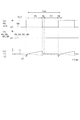
- FIG. 1 is a configuration diagram of a power conversion device according to the first embodiment.
- FIG. 2 is a functional block diagram of the control unit in the normal mode and the heat generation mode.
- FIG. 3 is a diagram showing the characteristics of the reverse conduction current flowing through the Gan-HEMT.
- FIG. 4 is a timing chart showing the transition of the operating state of each switch in the normal mode and the heat generation mode.
- FIG. 5 is a flowchart showing a processing procedure of the control unit.
- FIG. 6 is a timing chart showing current waveforms and the like in the normal mode and the heat generation mode.
- FIG. 7 is a diagram showing current paths in the normal mode and the heat generation mode.
- FIG. 8 is a configuration diagram of the power conversion device according to the second modification of the first embodiment.
- FIG. 9 is a timing chart showing the transition of the operation state of each switch in the normal mode and the heat generation mode.
- FIG. 10 is a diagram showing current paths in the normal mode and the heat generation mode.
- FIG. 11 is a configuration diagram of the power conversion device according to the second embodiment.
- FIG. 12 is a functional block diagram of the control unit in the normal mode and the heat generation mode.
- FIG. 13 is a flowchart showing a processing procedure of the control unit.
- FIG. 14 is a timing chart showing current waveforms and the like in the normal mode and the heat generation mode.
- FIG. 15 is a diagram showing a voltage control method of the gate voltage setting unit in the heat generation mode.
- FIG. 16 is a functional block diagram of the gate voltage setting unit in the heat generation mode.
- FIG. 17 is a timing chart showing a current waveform and the like in the heat generation mode of the fourth embodiment.
- FIG. 18 is a timing chart showing the transition of the operating state of each switch in the heat generation mode of the fifth embodiment.
- FIG. 19 is a timing chart showing the current path in the heat generation mode.
- FIG. 20 is a diagram showing the characteristics of the amount of conduction current and the amount of voltage drop when the gate voltage at the time of turning on is reduced.
- FIG. 21 is a functional block diagram of the control unit in the normal mode of the sixth embodiment.
- FIG. 22 is a timing chart showing the transition of the operating state of each switch in the normal mode.
- FIG. 23 is a configuration diagram of the power conversion device according to the seventh embodiment.
- the power conversion device of the present embodiment is mounted on an electrified vehicle such as a plug-in hybrid vehicle or an electric vehicle.
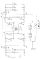
- the power conversion system includes a storage battery 10 as a power storage unit, a power supply target 11, a first capacitor 12, a second capacitor 13, and a power conversion device 20.
- the storage battery 10 supplies electric power to the power supply target 11 via the electric power conversion device 20.
- the storage battery 10 is a rechargeable and dischargeable secondary battery, for example, a lithium ion storage battery.
- the power supply target 11 includes at least one of a low-voltage storage battery having an output voltage lower than that of the storage battery 10 and an electric load.
- the low-voltage storage battery is, for example, a lead storage battery.
- the electric load is, for example, a headlamp or the like.
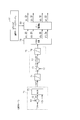
- the power conversion device 20 includes a first high potential side terminal CH1, a first low potential side terminal CL1, a first full bridge circuit 30, a second high potential side terminal CH2, a second low potential side terminal CL2, and a second full bridge circuit. It includes 40 and a transformer 50.
- the first high potential side terminal CH1 and the first low potential side terminal CL1 correspond to a pair of input side terminals
- the second high potential side terminal CH2 and the second low potential side terminal CL2 correspond to a pair of output sides.
- the first full bridge circuit 30 corresponds to the conversion circuit.
- the first full bridge circuit 30 includes first to fourth switches Q1 to Q4.
- the first to fourth switches Q1 to Q4 are N-channel MOSFETs.
- the second full bridge circuit 40 includes fifth to eighth switches Q5 to Q8.
- the fifth to eighth switches Q5 to Q8 are GaN-HEMTs.
- GaN is gallium nitride and HEMT is a high electron mobility transistor.
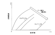
- the GaN-HEMT is a switching device having a characteristic that when a negative voltage is applied to the gate, the voltage drop at the time of reverse conduction increases.
- the fifth to eighth switches Q5 to Q8 correspond to the switch unit.
- the drain corresponds to the high potential side terminal and the source corresponds to the low potential side terminal.
- the first high potential side terminal CH1 is connected to the drains of the first switch Q1 and the third switch Q3.
- the drain of the second switch Q2 is connected to the source of the first switch Q1, and the drain of the fourth switch Q4 is connected to the source of the third switch Q3.
- the first low potential side terminal CL1 is connected to the sources of the second switch Q2 and the fourth switch Q4.
- the first low potential side terminal CL1 is connected to the first high potential side terminal CH1 via the first capacitor 12.
- the positive electrode terminal of the storage battery 10 is connected to the first high potential side terminal CH1, and the first low potential side terminal CL1 is connected to the negative electrode terminal of the storage battery 10.
- the second high potential side terminal CH2 is connected to the drains of the fifth switch Q5 and the seventh switch Q7.
- the drain of the sixth switch Q6 is connected to the source of the fifth switch Q5, and the drain of the eighth switch Q8 is connected to the source of the seventh switch Q7.
- the second low potential side terminal CL2 is connected to the sources of the sixth switch Q6 and the eighth switch Q8.
- the second low potential side terminal CL2 is connected to the second high potential side terminal CH2 via the second capacitor 13. Further, the second low potential side terminal CL2 is connected to the second high potential side terminal CH2 via the power supply target 11.
- the transformer 50 has a first coil 50a and a second coil 50b.
- the source of the first switch Q1 and the drain of the second switch Q2 are connected to the first end of the first coil 50a, and the source of the third switch Q3 and the fourth switch Q4 are connected to the second end of the first coil 50a. Drain is connected.
- the source of the fifth switch Q5 and the drain of the sixth switch Q6 are connected to the first end of the second coil 50b, and the source of the seventh switch Q7 and the eighth switch Q8 are connected to the second end of the second coil 50b. Drain is connected.
- the first coil 50a and the second coil 50b are magnetically coupled to each other.
- an induced voltage is generated in the second coil 50b so that the potential of the first end becomes higher than that of the second end.
- an induced voltage is generated in the second coil 50b so that the potential of the second end is higher than that of the first end.
- the power conversion system includes a first current sensor 60, a first voltage sensor 61, a second current sensor 62, a second voltage sensor 63, and a temperature sensor 64.
- the first current sensor 60 detects the first current I1 flowing through the first high potential side terminal CH1
- the first voltage sensor 61 detects the voltage between the terminals of the first high potential side terminal CH1 and the first low potential side terminal CL1.
- the first voltage V1 is detected.
- the first current I1 is positive when the discharge current flows through the storage battery 10 and negative when the charge current flows.
- the second current sensor 62 detects the second current I2 flowing through the second high potential side terminal CH2, and the second voltage sensor 63 detects the voltage between the terminals of the second high potential side terminal CH2 and the second low potential side terminal CL2.
- the second voltage V2 is detected.
- the second current I2 is positive when the current flows from the second high potential side terminal CH2 in the drain direction of the fifth switch Q5 and the seventh switch Q7, and negative when the current flows in the opposite direction. ..
- the temperature sensor 64 detects the environmental temperature T.
- the environmental temperature T is the temperature of the element to be heated.
- the element to be heated is, for example, the power conversion device 20.
- Each detected value I1, V1, I2, V2, T is input to the control unit 70 included in the power conversion device 20.
- the control unit 70 outputs a drive signal to the gates of the switches Q1 to Q8 based on the detected values I1, V1, I2, V2, T, and turns on and off the switches Q1 to Q8.
- the temperature rise control implemented in this embodiment will be described.
- the normal mode is set as there is no request for increasing the calorific value.
- the heat generation mode is set because there is a request to increase the heat generation amount.
- FIG. 2 shows a control block diagram carried out by the control unit 70 in the normal mode and the heat generation mode.
- the control unit 70 includes a command current setting unit 71.
- the command current setting unit 71 includes a current calculation unit 72 and a minimum value selection unit 73.
- the current calculation unit 72 calculates the command current I2f by dividing the power command value P2 * by the second voltage V2, which is the detection voltage of the second voltage sensor 63.
- the definition of the code of the command current I2f is the same as the definition of the code of the second current I2.
- the minimum value selection unit 73 selects the smaller of the command current I2f calculated by the current calculation unit 72 and the current limit value I2L as the final command current Iref2.
- the current limit value I2L is set to protect the power conversion system from overcurrent.
- the upper limit value or the lower limit value of the command current Iref2 output from the minimum value selection unit 73 is limited by the first limiter 74.
- the control unit 70 includes a current controller 75.
- the current controller 75 includes a current deviation calculation unit 76, a feedback control unit 77, and a second limiter 78.
- the current deviation calculation unit 76 calculates the current deviation ⁇ I2 by subtracting the second current I2, which is the detection current of the second current sensor 62, from the command current Iref2 output from the first limiter 74.
- the feedback control unit 77 calculates the inter-leg phase ⁇ 1 as an operation amount for feeding back the calculated current deviation ⁇ I2 to 0.
- proportional integral control is used as this feedback control.
- the feedback control used in the feedback control unit 77 is not limited to the proportional integral control, and may be, for example, the proportional integral differential control.
- the upper limit value or the lower limit value of the inter-leg phase ⁇ 1 calculated by the feedback control unit 77 is limited by the second limiter 78.
- the inter-leg phase ⁇ 1 is limited to a range from 0 ° to a predetermined phase, and in that range, the larger the value, the larger the power transmitted from the storage battery 10 to the power supply target 11.
- the control unit 70 includes a PWM generation unit 79, a gate voltage correction unit 80, and a gate voltage setting unit 81.
- the PWM generation unit 79 generates drive signals for the switches Q1 to Q8 based on the inter-leg phase ⁇ 1 received from the second limiter 78, and outputs the drive signals to the gate voltage correction unit 80.
- the PWM generation unit 79 generates a drive signal for turning on / off the first to fourth switches Q1 to Q4 and turning off the fifth to eighth switches Q5 to Q8.
- the gate voltage correction unit 80 corrects the gate voltage Voff when the fifth to eighth switches Q5 to Q8 are off, based on the command received from the gate voltage setting unit 81. After that, the gate voltage correction unit 80 outputs a drive signal reflecting the above correction to the gates of the switches Q1 to Q8.
- the gate voltage setting unit 81 sets the gate voltage Voff when the fifth to eighth switches Q5 to Q8 are off to the first off voltage V ⁇ (for example, 0V) in the normal mode, and the second in the heat generation mode.
- V ⁇ the first off voltage V ⁇
- the second off voltage V ⁇ is a value smaller than the first off voltage V ⁇ , and is a negative voltage in the present embodiment. Setting the off-time gate voltage Voff to the second off-voltage V ⁇ corresponds to increasing the off-time gate voltage Voff to the negative side.
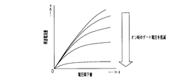
- FIG. 3 is a diagram showing the characteristics of the reverse conduction current flowing through the GaN-HEMT.
- the vertical axis shows the amount of reverse conduction current
- the horizontal axis shows the amount of voltage drop.
- FIG. 4 shows the transition of the operating state of each switch Q1 to Q8 in the normal mode and the heat generation mode.
- FIG. 4A shows the transition of the operating state of the first to fourth switches Q1 to Q4
- FIG. 4B shows the transition of the operating state of the fifth to eighth switches Q5 to Q8.
- the solid line in FIG. 4A shows the transition of the operating state of the first switch Q1.
- the operation state in which the operation state of the first switch Q1 is reversed becomes the operation state of the second switch Q2.
- the broken line in FIG. 4A shows the transition of the operating state of the third switch Q3.
- the operation state in which the operation state of the third switch Q3 is reversed becomes the operation state of the fourth switch Q4.
- the on period of the first switch Q1 is the off period of the second switch Q2.
- the solid line in FIG. 4B shows the operating state of the 5th to 8th switches Q5 to Q8.
- the fifth to eighth switches Q5 to Q8 are turned off.
- the 1 switching period Tsw of the 1st to 4th switches Q1 to Q4 is the same as each other.
- the phase difference between the off-switching timing of the first switch Q1 and the off-switching timing of the third switch Q3 is defined as the inter-leg phase ⁇ 1.
- the inter-leg phase ⁇ 1 becomes positive when the switching timing of the third switch Q3 to the off is earlier than the switching timing of the first switch Q1 to the off.
- the inter-leg phase ⁇ 1 is positive.
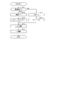
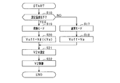
- FIG. 5 shows a procedure of processing executed by the control unit 70. This process is repeatedly executed, for example, at a predetermined control cycle.
- the product of the number of turns of the first voltage V1 and the first coil 50a is larger than the product of the number of turns of the second voltage V2 and the second coil 50b. That is, it is assumed that the electric power is transmitted from the storage battery 10 to the power supply target 11 by this process.
- step S10 it is determined whether the environmental temperature T is equal to or lower than the set temperature.
- step S10 corresponds to the determination unit.
- step S10 If a negative determination is made in step S10, the process proceeds to step S11 assuming that there is no request to increase the calorific value, and the control mode is set to the normal mode. In the normal mode, in the next step S12, the gate voltage Voff when the fifth to eighth switches Q5 to Q8 are off is set to the first off voltage V ⁇ .
- step S10 If an affirmative judgment is made in step S10, the process proceeds to step S13 on the assumption that there is a request to increase the amount of heat generated, and the control mode is set to the heat generation mode.
- the gate voltage Voff when the fifth to eighth switches Q5 to Q8 are off is set to the second off voltage V ⁇ .
- step S15 the command current setting unit 71 sets the command current Iref2.
- step S16 the first to fourth switches Q1 to Q4 are turned on and off, and the fifth to eighth switches Q5 to Q8 are turned off so that the second current I2 is controlled by the command current Iref2.
- FIG. 6 shows the transition of the operation state and the like of each switch Q1 to Q8 in the normal mode and the heat generation mode.
- FIG. 6A shows the transition of the operating state of the first to fourth switches Q1 to Q4.
- FIG. 6B shows the transition of the operating state of the 5th to 8th switches Q5 to Q8.
- FIG. 6C shows the transition of the first current I1 and the second current I2.
- FIG. 6D shows the first power P1, the second power P2, and the lost power P1 + P2.
- the first electric power P1 is the time average value of the electric power supplied from the storage battery 10 to the first full bridge circuit 30, and the second electric power P2 is supplied from the second full bridge circuit 40 to the power supply target 11. It is the time average value of the electric power to be generated.
- the first electric power P1 is positive, the storage battery 10 is discharged. Further, when the second electric power P2 is negative, electric power is supplied to the power supply target 11. Therefore, the sum P1 + P2 of the first power P1 and the second power P2 is the lost power.
- FIG. 6E is an enlarged view of the vertical axis of the power loss P1 + P2 in FIG. 6D.
- the scales of the vertical axis in the normal mode and the heat generation mode of FIG. 6 (e) are the same, and are used to compare the magnitudes of the power loss P1 + P2 in the normal mode and the heat generation mode.
- the inter-leg phase ⁇ 1 is set to a value in the range from 0 ° to a predetermined phase so that the second current I2 is feedback-controlled by the command current Iref2.
- the inter-leg phase ⁇ 1 By limiting the inter-leg phase ⁇ 1 to a range from 0 ° to a predetermined phase, it is possible to prevent the inter-leg phase ⁇ 1 from becoming too large and reducing the power that can be transmitted from the storage battery 10 to the power supply target 11.
- the first to fourth periods T1 to T4 appear in one switching cycle Tsw.
- the switching patterns of the normal mode and the heat generation mode are the same.
- the first period T1 the second and third switches Q2 and Q3 are turned on, and the first, fourth, fifth, sixth, seventh and eighth switches Q1, Q4, Q5, Q6 and Q7.
- Q8 is the period during which it is turned off.
- the second period T2 the first, third switches Q1 and Q3 are turned on, and the second, fourth, fifth, sixth, seventh, and eighth switches Q2, Q4, Q5, Q6, and Q7.
- Q8 is the period during which it is turned off.
- the first and fourth switches Q1 and Q4 are turned on, and the second, third, fifth, sixth, seventh, and eighth switches Q2, Q3, Q5, Q6, and Q7. , Q8 is the period during which it is turned off.
- the second and fourth switches Q2 and Q4 are turned on, and the first, third, fifth, sixth, seventh, and eighth switches Q1, Q3, Q5, Q6, and Q7. , Q8 is the period during which it is turned off.
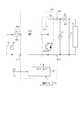
- FIG. 7A shows the current path in the first period T1.
- a current path including the first high potential side terminal CH1, the third switch Q3, the first coil 50a, the second switch Q2, and the first low potential side terminal CL1 is formed.
- the second full bridge circuit 40 a current path including the second low potential side terminal CL2, the sixth switch Q6, the second coil 50b, the seventh switch Q7, and the second high potential side terminal CH2 is formed.
- the 6th switch Q6 and the 7th switch Q7 are turned off, but due to the characteristics of the GaN-HEMT, a reverse conduction current is flowing through the 6th switch Q6 and the 7th switch Q7.
- the first current I1 gradually increases in the positive direction and the second current I2 gradually increases in the negative direction.
- the gate voltage Voff at the time of off is increased to the negative side as compared with the normal mode. Therefore, due to the characteristics of GaN-HEMT, the reverse conduction current of the sixth switch Q6 and the seventh switch Q7 The conduction loss due to is larger than that in the normal mode.
- FIG. 7B shows the current path in the second period T2.
- a current path including the first switch Q1, the third switch Q3, and the first coil 50a is formed.
- the second full bridge circuit 40 the same current path as in the first period T1 is formed.
- the first coil 50a is not connected to the first low potential side terminal CL1, so that the first current I1 is 0 as shown in FIG. 6C.
- the first full bridge circuit 30 an induced voltage is temporarily generated in the first coil 50a so that the potential at the first end is higher than that at the second end.
- an induced voltage is temporarily generated in the second coil 50b so that the potential at the second end is higher than that at the first end. Therefore, the sign of the second current I2 remains negative, and its absolute value gradually decreases. Even in this case, due to the characteristics of GaN-HEMT, the conduction loss due to the reverse conduction current is larger in the heat generation mode than in the normal mode.
- FIG. 7 (c) shows the current path in the third period T3.
- a current path including the first high potential side terminal CH1, the first switch Q1, the first coil 50a, the fourth switch Q4, and the first low potential side terminal CL1 is formed.
- the second full bridge circuit 40 a current path including the second low potential side terminal CL2, the eighth switch Q8, the second coil 50b, the fifth switch Q5, and the second high potential side terminal CH2 is formed.
- the fifth switch Q5 and the eighth switch Q8 are turned off, but due to the characteristics of the GaN-HEMT, a reverse conduction current is passed through the fifth switch Q5 and the eighth switch Q8.
- the first current I1 gradually increases in the positive direction and the second current I2 gradually increases in the negative direction.
- the gate voltage Voff at the time of off is increased to the negative side as compared with the normal mode. Therefore, due to the characteristics of GaN-HEMT, the reverse conduction current of the fifth switch Q5 and the eighth switch Q8 The conduction loss due to is larger than that in the normal mode.
- FIG. 7 (d) shows the current path in the fourth period T4.
- a current path including the second switch Q2, the first coil 50a, and the fourth switch Q4 is formed.
- the second full bridge circuit 40 the same current path as in the third period T3 is formed.
- the first coil 50a is not connected to the first high potential side terminal CH1, so that the first current I1 is 0 as shown in FIG. 6C.
- the first full bridge circuit 30 an induced voltage is temporarily generated in the first coil 50a so that the potential at the second end is higher than that at the first end.
- an induced voltage is temporarily generated in the second coil 50b so that the potential at the first end is higher than that at the second end. Therefore, the sign of the second current I2 remains negative, and its absolute value gradually decreases. Even in this case, due to the characteristics of GaN-HEMT, the conduction loss due to the reverse conduction current is larger in the heat generation mode than in the normal mode.
- FIG. 6C shows the time average value I1ave of the first current I1 and the time average value I2ave of the second current I2 in the first to fourth periods T1 to T4 with broken lines.
- the first current average value I1ave is a positive value
- the second current average value I2ave is a negative value.
- the first power P1 has a positive value
- the second power P2 has a negative value. This indicates that the electric power was transmitted from the storage battery 10 to the power supply target 11 in the first period T1 to the fourth period T4. Since power loss occurs in each of the switches Q1 to Q8 and the like due to this power transmission, the lost power P1 + P2 is a positive value.
- the power loss P1 + P2 in the heat generation mode is larger than the value of the power loss P1 + P2 in the normal mode. This is because in the heat generation mode, the gate voltage Voff at off is increased to the negative side as compared with the normal mode, and therefore, due to the characteristics of GaN-HEMT, the conduction loss due to the reverse conduction current in the 5th to 8th switches Q5 to Q8. This is because
- the fifth to eighth switches Q5 to Q8 are turned off when power is transmitted from the storage battery 10 to the power supply target 11. At this time, a conduction loss is generated as the reverse conduction current flows through the 5th to 8th switches Q5 to Q8, and heat is generated by the conduction loss.
- the power conversion device 20 can be miniaturized.
- the fifth to eighth switches Q5 to Q8 of the present embodiment are composed of GaN-HEMT, when a reverse conduction current flows, the larger the gate voltage Voff at the time of off is on the negative side, the more it occurs. It has the characteristic that the conduction loss is large. Focusing on this characteristic, in the present embodiment, when the heat generation mode is set, the gate voltage Voff when the 5th to 8th switches Q5 to Q8 are off increases to the negative side as compared with the case where the normal mode is set. Will be done. As a result, the conduction loss generated in the fifth to eighth switches Q5 to Q8 when the heat generation mode is set can be made larger than that when the normal mode is set. As a result, the amount of heat generated by the power conversion device 20 can be increased.
- the first to fourth switches Q1 to Q4 are not limited to N-channel MOSFETs, and may be IGBTs.
- the high potential side terminal is the collector and the low potential side terminal is the emitter.
- the first full bridge circuit 30 includes a freewheel diode connected in antiparallel to each of the first to fourth switches Q1 to Q4. In this case, the pair of the switch and the freewheel diode corresponds to the switch portion.
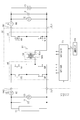
- FIG. 8 is a configuration diagram of this embodiment.
- the power conversion system includes a power conversion device 90.
- the power conversion device 90 includes a third capacitor 91 and a half-bridge circuit 92.
- the half-bridge circuit 92 corresponds to the conversion circuit.
- the half-bridge circuit 92 includes a ninth switch Q9 and a tenth switch Q10.
- the 9th switch Q9 and the 10th switch Q10 are N-channel MOSFETs.
- the first high potential side terminal CH1 is connected to the drain of the ninth switch Q9.
- the drain of the 10th switch Q10 is connected to the source of the 9th switch Q9.
- the first low potential side terminal CL1 and the second end of the first coil 50a are connected to the source of the tenth switch Q10.
- the source of the 9th switch Q9 and the drain of the 10th switch Q10 are connected to the first end of the first coil 50a via the third capacitor 91.
- the control unit 70 alternately turns on the ninth switch Q9 and the tenth switch Q10 constituting the half-bridge circuit 92.
- the duty ratio of the ninth switch Q9 is 0.5.
- the duty ratio is the ratio (Ton / Tsw) of the on-time Ton to the one switching cycle Tsw of the ninth switch Q9.
- FIG. 9 shows changes in the operating states of the fifth to tenth switches Q5 to Q10 in the normal mode and the heat generation mode of the present embodiment.
- the solid line in FIG. 9A shows the transition of the operating state of the 9th switch Q9, and the broken line shows the transition of the 10th switch Q10.
- FIG. 9B shows the operating states of the 5th to 8th switches Q5 to Q8.
- FIG. 9C shows the transition of the first current I1 and the second current I2.
- the fifth to eighth periods T5 to T8 appear in one switching cycle Tsw.
- the ninth switch Q9 is turned on, and the fifth, sixth, seventh, eighth, and tenth switches Q5, Q6, Q7, Q8, and Q10 are turned off.
- the 10th switch Q10 is turned on, and the 5th, 6th, 6th, 7th, 8th, and 9th switches Q5, Q6, Q7, Q8, and Q9 are turned off.
- the period. As described above, also in this embodiment, since the fifth to eighth switches Q5 to Q8 constituting the second full bridge circuit 40 are fixed to off, conduction loss due to the reverse conduction current occurs.
- FIG. 10A shows the current path in the fifth period T5.
- a current path including the first high potential side terminal CH1, the ninth switch Q9, the third capacitor 91, the first coil 50a, and the first low potential side terminal CL1 is formed.
- the second full bridge circuit 40 the same current path as in the third period T3 is formed.
- the first current I1 gradually increases in the positive direction in the fifth period T5.
- the second current I2 gradually increases in the negative direction.
- FIG. 10B shows the current path in the sixth period T6.
- a current path including the 10th switch Q10, the 3rd capacitor 91, and the 1st coil 50a is formed in the half-bridge circuit 92.
- the same current path as in the fifth period T5 is formed in the second full bridge circuit 40.
- the first current I1 is 0 as shown in FIG. 9C.
- the half-bridge circuit 92 an induced voltage is temporarily generated in the first coil 50a so that the potential at the second end is higher than that at the first end.
- an induced voltage is temporarily generated in the second coil 50b so that the potential at the first end is higher than that at the second end. Therefore, the sign of the second current I2 remains negative, and its absolute value gradually decreases.
- FIG. 10 (c) shows the current path in the 7th period T7.
- a current in the opposite direction flows in the same current path as in the sixth period T6.
- a current path including the second low potential side terminal CL2, the sixth switch Q6, the second coil 50b, the seventh switch Q7, and the second high potential side terminal CH2 is formed.
- the 1st current I1 is 0 as shown in FIG. 9C. Since the electric charge stored in the third capacitor 91 is discharged to the half-bridge circuit 92, a current flows in the direction opposite to that of the sixth period T6. Therefore, an induced voltage is generated in the second coil 50b so that the potential at the second end is higher than that at the first end. Therefore, the second current I2 gradually increases in the negative direction.
- FIG. 10 (d) shows the current path in the eighth period T8.
- a current path including the first low potential side terminal CL1, the second coil 50b, the third capacitor 91, the ninth switch Q9, and the first high potential side terminal CH1 is formed.
- the second full bridge circuit 40 the same current path as in the seventh period T7 is formed.
- an induced voltage is temporarily generated in the first coil 50a so that the potential at the first end is higher than that at the second end. Therefore, as shown in FIG. 9C, the sign of the first current I1 becomes negative, and its absolute value gradually decreases.
- an induced voltage is temporarily generated in the second coil 50b so that the potential at the second end is higher than that at the first end. Therefore, the sign of the second current I2 remains negative, and its absolute value gradually decreases.
- the half-bridge circuit 92 is used as the configuration of the conversion circuit, the DC voltage supplied from the storage battery 10 can be converted into an alternating voltage. Therefore, using this alternating voltage, a reverse conduction current can be passed through the fifth to eighth switches Q5 to Q8 constituting the second full bridge circuit 40.
- the tenth switch Q10 is not limited to the N-channel MOSFET, but may be an IGBT.
- the second embodiment will be described with reference to the drawings, focusing on the differences from the first embodiment.
- a full bridge circuit is used in the configuration of the power conversion device 20, but this is changed.
- the configuration of the power conversion device is a step-up chopper circuit.
- FIG. 11 shows a configuration diagram of this embodiment.
- the power conversion system includes a storage battery 10, a power supply target 11, a capacitor 12, and a power conversion device 100.
- the power conversion device 100 includes a first high potential side terminal CH1, a first low potential side terminal CL1, a second high potential side terminal CH2, a second low potential side terminal CL2, a half bridge circuit 101, and a reactor 102. ..
- the half-bridge circuit 101 includes an eleventh switch Q11 and a twelfth switch Q12.
- the eleventh switch Q11 is a GaN-HEMT and the twelfth switch Q12 is an IGBT.
- the second high potential side terminal CH2 is connected to the drain of the eleventh switch Q11.
- the collector of the 12th switch Q12 is connected to the source of the 11th switch Q11.
- the first low potential side terminal CL1 and the second low potential side terminal CL2 are connected to the emitter of the twelfth switch Q12.
- the second low potential side terminal CL2 is connected to the second high potential side terminal CH2 via the capacitor 12. Further, the second low potential side terminal CL2 is connected to the second high potential side terminal CH2 via the power supply target 11.
- a diode D as a freewheel diode is connected in antiparallel to the 12th switch Q12.
- the twelfth switch Q12 is not limited to the IGBT, and an N-channel MOSFET may be used. In this case, the diode D may not be provided.
- the first end of the reactor 102 is connected to the first high potential side terminal CH1.
- the second end of the reactor 102 is connected to the source of the 11th switch Q11 and the collector of the 12th switch Q12.
- the positive electrode terminal of the storage battery 10 is connected to the first high potential side terminal CH1, and the first low potential side terminal CL1 is connected to the negative electrode terminal of the storage battery 10.
- the power conversion system includes a first current sensor 60, a first voltage sensor 61, a second current sensor 62, a second voltage sensor 63, and a temperature sensor 64.
- the detection target of these sensors is the same as that of the first embodiment.
- the control unit 70 outputs a drive signal to the gates of the 11th switch Q11 and the 12th switch Q12 based on the detected values I1, V1, I2, V2, T, and turns the 11th switch Q11 and the 12th switch Q12 on and off.
- the definition of the code of the first current I1 is the same as that of the first embodiment, but the second current I2 is a case where a current flows from the second high potential side terminal CH2 in the direction of the power supply target 11. Is positive, and the case where current flows in the opposite direction is negative.
- FIG. 12 is a control block diagram implemented by the control unit 70 in this embodiment.
- the control unit 70 includes a voltage controller 82.
- the voltage controller 82 includes a voltage deviation calculation unit 83, a feedback control unit 77, and a duty ratio calculation unit 84.
- the voltage deviation calculation unit 83 calculates the voltage deviation ⁇ V2 by subtracting the second voltage V2, which is the detection voltage of the second voltage sensor 63, from the command voltage V2 *.
- the feedback control unit 77 calculates the duty ratio of the 12th switch Q12 as an operation amount for feeding back the calculated voltage deviation ⁇ V2 to 0.
- the duty ratio calculation unit 84 adds the feedforward term (V2 * -V1) / V2 * to the duty ratio calculated by the feedback control unit 77 to obtain the final duty ratio of the 12th switch Q12.
- the duty ratio of the 12th switch Q12 is output to the PWM generation unit 79.
- the PWM generation unit 79 generates drive signals for the 11th switch Q11 and the 12th switch Q12 and outputs them to the gate voltage correction unit 85.
- the eleventh switch Q11 is turned off.
- the twelfth switch Q12 is turned on and off based on the duty ratio of the twelfth switch Q12.
- the gate voltage correction unit 85 corrects the gate voltage Voff when the 11th switch Q11 is off, based on the command received from the gate voltage setting unit 81. After that, the gate voltage correction unit 85 outputs the drive signal to the 11th switch Q11 and the 12th switch Q12.
- the gate voltage setting unit 81 sets the gate voltage Voff when the eleventh switch Q11 is off, as in the first embodiment.
- FIG. 13 shows a procedure of processing executed by the control unit 70. This process is repeatedly executed, for example, at a predetermined control cycle.
- FIG. 13 the same processing as that shown in FIG. 5 above is designated by the same reference numerals for convenience.
- step S10 If a negative determination is made in step S10, the process proceeds to step S17 assuming that there is no request to increase the calorific value, and the control mode is set to the normal mode. In the normal mode, in the next step S18, the gate voltage Voff when the eleventh switch Q11 is off is set to the first off voltage V ⁇ .
- step S10 If an affirmative judgment is made in step S10, the process proceeds to step S19 on the assumption that there is a request to increase the amount of heat generated, and the control mode is set to the heat generation mode.
- the gate voltage Voff when the 11th switch Q11 is off is set to the second off voltage V ⁇ .
- the second off voltage V ⁇ is a value increased to the negative side of the first off voltage V ⁇ .
- step S21 the value of the command voltage V2 * is set.
- step S22 the eleventh switch Q11 is turned off, and the duty ratio of the twelfth switch Q12 is controlled so that the second voltage V2 is controlled by the command voltage V2 *.
- FIG. 14 shows changes in the operating states of the 11th switch Q11 and the 12th switch Q12 in the normal mode and the heat generation mode.
- the solid line in FIG. 14A shows the transition of the operating state of the 11th switch Q11, and the broken line shows the transition of the operating state of the 12th switch Q12.
- FIG. 14B shows a first voltage V1 and a second voltage V2.
- FIG. 14C shows the transition of the first current I1 and the second current I2.
- FIG. 14D shows the first power P1, the second power P2, and the lost power P1-P2.
- the case where the second electric power P2 is supplied from the electric power conversion device 100 to the power supply target 11 is positive. Therefore, the value obtained by subtracting the second power P2 from the first power P1 is the lost power P1-P2.
- the power loss P1-P2 in the heat generation mode is larger than the power loss P1-P2 in the normal mode. This is because, also in the present embodiment, in the heat generation mode, the gate voltage Voff at the time of off is increased to the negative side as compared with the normal mode. Therefore, due to the characteristics of GaN-HEMT, the conduction due to the reverse conduction current in the 11th switch Q11 This is because the loss becomes large.
- the gate voltage setting unit 81 controls the gate voltage Voff when the fifth to eighth switches Q5 to Q8 are off based on the environmental temperature T.
- FIG. 15 shows a voltage control method implemented by the gate voltage setting unit 81.
- the upper limit temperature TL is a temperature set from the heat resistance of the element to be heated, and is set to, for example, the allowable upper limit temperature of the element to be heated.
- the gate voltage setting unit 81 sets the gate voltage Voff when the fifth to eighth switches Q5 to Q8 are off. Set to a value according to the temperature T. Specifically, when the environmental temperature T exceeds the limit start temperature TC, the gate voltage setting unit 81 sets the gate voltage Voff when the fifth to eighth switches Q5 to Q8 are off as the environmental temperature T approaches the upper limit temperature TL.
- the gate voltage setting unit 81 sets the gate voltage Voff when the fifth to eighth switches Q5 to Q8 are off to the first off voltage V ⁇ .
- the gate voltage Voff when the fifth to eighth switches Q5 to Q8 set in this way are off is output to the gate voltage correction unit 80.
- the gate voltage Voff at the time of off is set to the first off voltage V ⁇ .
- the off gate voltage Voff is set to the second off voltage V ⁇ .
- the gate voltage Voff of the 5th to 8th switches Q5 to Q8 is gradually reduced based on the environmental temperature T to reduce heat generation due to the reverse conduction current. be able to. As a result, it is possible to prevent the environmental temperature T from exceeding the upper limit temperature TL.
- FIG. 16 is a control block diagram implemented by the gate voltage setting unit 81 in the heat generation mode of the present embodiment.
- the gate voltage setting unit 81 includes a temperature controller 86.
- the temperature controller 86 includes a temperature deviation calculation unit 87, a feedback control unit 88, and a limiter 89.
- the temperature deviation calculation unit 87 calculates the temperature deviation ⁇ T by subtracting the environmental temperature T from the target temperature T *.
- the target temperature T * corresponds to the command temperature.
- the feedback control unit 88 calculates the gate voltage Voff when the fifth to eighth switches Q5 to Q8 are off as the operation amount for feeding back the calculated temperature deviation ⁇ T to 0. For example, when the environmental temperature T is raised, the gate voltage Voff at the time of off is increased to the negative side. On the other hand, when the environmental temperature T is lowered, the absolute value of the gate voltage Voff at the time of off is reduced.
- proportional integral control is used as this feedback control.
- the feedback control used in the feedback control unit 88 is not limited to the proportional integral control, and may be, for example, the proportional integral differential control.
- the upper limit value or lower limit value of the gate voltage Voff when the fifth to eighth switches Q5 to Q8 calculated by the feedback control unit 88 is off is limited by the limiter 89, and is output to the gate voltage correction unit 80.
- the upper limit value is the first off voltage V ⁇
- the lower limit value is the voltage determined from the characteristics of the fifth to eighth switches Q5 to Q8.
- the environmental temperature T can be controlled to the target temperature T *.
- control unit 70 temporarily switches the gate voltage Voff when the fifth switch Q5 and the sixth switch Q6 are off from the second off voltage V ⁇ to the first off voltage V ⁇ .
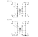
- FIG. 17 shows the transition of the operating state and the like of the switches Q1 to Q8 in each of the case where the gate voltage Voff at the time of off is fixed and the case where the gate voltage Voff at the time of off is temporarily switched.
- FIG. 17A shows the transition of the operating state of the first switch Q1 and the fourth switch Q4. The operating state in which the operating states of the first switch Q1 and the fourth switch Q4 are reversed becomes the operating state of the second switch Q2 and the third switch Q3.
- FIG. 17B shows the transition of the operating state of the fifth to eighth switches Q5 to Q8. Also in this embodiment, the fifth to eighth switches Q5 to Q8 are turned off.
- FIG. 17C shows the transition of the gate voltage Voff when the fifth switch Q5 and the sixth switch Q6 are off.
- FIG. 17D shows the transition of the first current I1 and the second current I2.
- the control unit 70 fixes the gate voltage Voff when the fifth switch Q5 and the sixth switch Q6 are off to the second off voltage V ⁇ .
- the control unit 70 temporarily switches the gate voltage Voff at the time of off from the second off voltage V ⁇ to the first off voltage V ⁇ .
- the control unit 70 controls the gate voltage Voff when the sixth switch Q6 is off to the first off voltage V ⁇ .
- the operating states of the switches Q1 to Q8 in the ninth period T9 are the same as those in the first period T1.
- the current path of the 9th period T9 is the same as that of the 1st period T1.
- the gate voltage Voff when the sixth switch Q6 is off is switched from the second off voltage V ⁇ to the first off voltage V ⁇ , so that the voltage drop amount of the sixth switch Q6 becomes smaller.
- the conduction loss of the sixth switch Q6 becomes smaller. Therefore, as shown in FIG. 17D, the second current I2 increases to the negative side in the case of Voff switching as compared with the case of Voff fixing. The speed will increase.
- the operating states of the switches Q1 to Q8 in the 10th period T10 are the same as those in the 3rd period T3.
- the current path of the 10th period T10 is the same as that of the 3rd period T3.
- the gate voltage Voff when the fifth switch Q5 is off is switched from the second off voltage V ⁇ to the first off voltage V ⁇ , so that the voltage drop amount of the fifth switch Q5 becomes smaller.
- the conduction loss of the fifth switch Q5 becomes small, as shown in FIG. 17D, when the Voff is switched, the second current I2 is moved to the negative side as compared with the case where the Voff is fixed. Increases the rate of increase.
- the control unit 70 sets the gate voltage Voff at the time of turning off the switch through which the reverse conduction current is flowing to the first off voltage within the period when the fifth to eighth switches Q5 to Q8 are turned off.
- a period for temporarily switching to V ⁇ is provided.
- the reverse conduction current is increased during this period, so that the gate voltage Voff at the time of off is returned to the second off voltage V ⁇ .
- the reverse conduction current can be passed through the 5th to 8th switches Q5 to Q8. As a result, the conduction loss due to the reverse conduction current can be increased, so that the amount of heat generated by the power conversion device 20 can be increased.
- the value for temporarily switching the gate voltage Voff at the time of off is set to the first off voltage V ⁇ , but this value is not limited to the first off voltage V ⁇ , and the magnitude of the reverse conduction current is adjusted. Therefore, it may be adjusted in a direction in which the conduction loss is reduced.
- the time width for temporarily switching the gate voltage Voff when off is increased, the reverse conduction current increases, but the amount of heat generated by the reverse conduction current decreases. Therefore, if the time width for temporarily switching the gate voltage Voff at the time of off is increased, the calorific value per switching cycle reaches the maximum value and then starts to decrease.
- a desired calorific value can be obtained as the time width for temporarily switching the gate voltage Voff at the time of off. It may be set to the time width.
- the fifth embodiment will be described with reference to the drawings, focusing on the differences from the first embodiment.
- the switching pattern in the heat generation mode is changed.
- the fifth to eighth switches Q5 to Q8 are turned off in the heat generation mode, but in the present embodiment, the fifth to eighth switches Q5 to Q8 are turned on and off.
- FIG. 18 shows the transition of the operating state and the like of the switches Q1 to Q8 in the heat generation mode of the present embodiment.
- the solid line in FIG. 18A shows the transition of the operating state of the first switch Q1.
- the operation state in which the operation state of the first switch Q1 is reversed becomes the operation state of the second switch Q2.
- the broken line in FIG. 18A shows the operating state of the fourth switch Q4.
- the operation state in which the operation state of the fourth switch Q4 is reversed becomes the operation state of the third switch Q3.
- the solid line in FIG. 18B shows the transition of the operating state of the fifth switch Q5.
- the operation state in which the operation state of the fifth switch Q5 is reversed becomes the operation state of the sixth switch Q6.
- the broken line in FIG. 18B shows the transition of the operating state of the eighth switch Q8.
- the operation state in which the operation state of the eighth switch Q8 is reversed becomes the operation state of the seventh switch Q7.
- the transmitted power between the first full bridge circuit 30 and the second full bridge circuit 40 is adjusted by controlling the intercircuit phase ⁇ 21.
- the inter-circuit phase ⁇ 21 is the phase difference between the on-switching timing of the fourth switch Q4 and the on-switching timing of the eighth switch Q8.
- FIG. 18C shows the transition of the gate voltage of the 5th switch Q5 and the 8th switch Q8.
- Von1 indicates the on-time gate voltage in the normal mode
- Von2 indicates the on-time gate voltage in the heat generation mode.
- the gate voltage Von2 at the time of turning on in the heat generation mode is reduced as compared with the gate voltage Von1 at the time of turning on in the normal mode.
- Voff1 indicates the gate voltage at the time of off in the normal mode
- Voff2 indicates the gate voltage at the time of off in the heat generation mode.
- the gate voltage Voff2 at the time of off in the heat generation mode is increased to the negative side as compared with the gate voltage Voff1 at the time of off in the normal mode. For example, in the eleventh period T11 shown in FIG.
- the gate voltage when the fifth switch Q5 and the eighth switch Q8 are on is set to Von2. Further, in the 12th period T12, the gate voltage when the fifth switch Q5 is on is set to Von2, and the gate voltage when the eighth switch Q8 is off is set to Voff2.
- the 1st, 4th, 5th, and 8th switches Q1, Q4, Q5, and Q8 are turned on, and the 2nd, 3rd, 6th, and 7th switches Q2, Q3, and Q6. This is the period during which Q7 is turned off.
- the current path of the 11th period T11 is the same as that of the 3rd period T3.
- the fifth switch Q5 and the eighth switch Q8 are turned on. Therefore, the control unit 70 sets the gate voltage at the time of turning on the fifth switch Q5 and the eighth switch Q8 through which the reverse conduction current flows to Von2, which is smaller than the gate voltage Von1 at the time of turning on in the normal mode.
- the conduction loss at the time of conduction can be increased.
- the second, third, fifth, and seventh switches Q2, Q3, Q5, and Q7 are turned on, and the first, fourth, sixth, and eighth switches Q1, Q4, and Q6. This is the period during which Q8 is turned off.
- FIG. 19B shows the current path of the 12th period T12.
- a circuit including the second coil 50b, the seventh switch Q7, and the fifth switch Q5 is formed.
- the control unit 70 sets the gate voltage at the time of turning on the fifth switch Q5 through which the forward conducting current flows to Von2, which is smaller than the gate voltage Von1 at the time of turning on in the normal mode. The conduction loss can be increased.
- FIG. 20 shows the characteristics of the forward conduction current amount and the voltage drop amount when the gate voltage when the fifth to eighth switches Q5 to Q8 are turned on is reduced.
- the arrows in FIG. 20 indicate that the gate voltage when on is reduced. It can be seen that when the gate voltage at the time of ON is reduced, the amount of voltage drop for the same amount of forward conduction current increases.
- the present embodiment by reducing the gate voltage at the time of turning on in the heat generation mode as compared with the normal mode, the voltage drop amount of the fifth to eighth switches Q5 to Q8 is increased, and the conduction loss is increased. be able to.
- the fifth to eighth switches Q5 It is also possible to reduce the stress applied to Q8. As a result, deterioration of the fifth to eighth switches Q5 to Q8 can be suppressed.
- FIG. 21 shows a control block diagram carried out by the control unit 70 in the normal mode.
- the same components as those in FIG. 2 above are designated by the same reference numerals for convenience.
- the feedback control unit 77 calculates the inter-circuit phase ⁇ 21 as an operation amount for feeding back the current deviation ⁇ I2 to 0.
- the inter-circuit phase ⁇ 21 is limited to a range from 0 ° to a predetermined phase, and in that range, the larger the value, the larger the transmitted power from the storage battery 10 to the power supply target 11.
- the PWM generation unit 79 generates drive signals for the switches Q1 to Q8 based on the inter-circuit phase ⁇ 21.
- FIG. 22 shows the transition of the operating state of each switch Q1 to Q8 in the normal mode.
- the solid line in FIG. 22A shows the transition of the operating state of the first switch Q1.
- the operation state in which the operation state of the first switch Q1 is reversed becomes the operation state of the second switch Q2.
- the broken line in FIG. 22A shows the transition of the operating state of the third switch Q3.
- the operation state in which the operation state of the third switch Q3 is reversed becomes the operation state of the fourth switch Q4.
- the solid line in FIG. 22B shows the transition of the operating state of the fifth switch Q5.
- the operation state in which the operation state of the fifth switch Q5 is reversed becomes the operation state of the sixth switch Q6.
- the broken line in FIG. 22B shows the transition of the operating state of the seventh switch Q7.
- the operation state in which the operation state of the seventh switch Q7 is reversed becomes the operation state of the eighth switch Q8.
- the phase difference between the on-switching timing of the first switch Q1 and the on-switching timing of the fifth switch Q5 is defined as the inter-circuit phase ⁇ 21.
- FIG. 23 shows a configuration diagram of this embodiment.
- the power conversion device 20 includes a heat transfer unit 110.
- the heat transfer unit 110 has each switch Q1 to Q8, a transformer 50, and a power supply target 11 as heat exchange target elements, and is configured to be able to absorb heat generated by the heat exchange target elements.
- the heat transfer unit 110 transfers the absorbed heat to the element to be heated, and raises the temperature of the element to be heated.
- the element to be heated is, for example, the power supply target 11.
- the heat transfer unit 110 includes, for example, a circulation path in which cooling water circulates between the heat exchange target element and the temperature rise target element, and raises the temperature of the temperature rise target element through the cooling water. May be good.
- the heat transfer unit 110 may use, for example, a gas (air) as the cooling fluid.
- the heat transfer unit 110 may be, for example, a constituent member such as a heat sink that comes into contact with the heat exchange target element and the temperature rise target element without using a cooling fluid.
- the heat generated by the power conversion can be recovered and transferred to the element to be heated, so that the temperature of the element to be heated can be efficiently increased.
- the circuit configuration of the power conversion device 20 of the first embodiment is used, but the modified example 2 of the first embodiment is used.
- the same effect can be obtained by using the circuit configuration of the power conversion device 90 shown in 1.
- the controls and methods thereof described in the present disclosure are provided by a dedicated computer provided by configuring a processor and memory programmed to perform one or more functions embodied by a computer program. It may be realized. Alternatively, the controls and methods thereof described in the present disclosure may be implemented by a dedicated computer provided by configuring the processor with one or more dedicated hardware logic circuits. Alternatively, the control unit and method thereof described in the present disclosure may be a combination of a processor and memory programmed to perform one or more functions and a processor composed of one or more hardware logic circuits. It may be realized by one or more dedicated computers configured. Further, the computer program may be stored in a computer-readable non-transitional tangible recording medium as an instruction executed by the computer.
Landscapes
- Engineering & Computer Science (AREA)
- Power Engineering (AREA)
- Transportation (AREA)
- Mechanical Engineering (AREA)
- Inverter Devices (AREA)
- Dc-Dc Converters (AREA)
- Electric Propulsion And Braking For Vehicles (AREA)
Abstract
電力変換装置(20,90,100)は、入力側端子(CH1,CL1)、出力側端子(CH1,CL1)及びスイッチ部(Q5~Q8,Q11)を有し、入力側端子に接続される蓄電部(10)から、出力側端子に接続される給電対象(11)へと電力伝達を行う場合にスイッチ部をオンオフする。スイッチ部は、スイッチ部に逆導通電流が流れる場合において、そのゲート電圧が負側に大きいほど、逆導通電流が流れる場合に発生する導通損失が大きくなる特性を有している。また、電力変換装置は、電力伝達に伴う発熱量の増大要求があるか否かを判定し、増大要求があると判定した場合、増大要求がないと判定した場合に比べて電力伝達を行うときに逆導通電流が流れるスイッチ部のオフ時のゲート電圧を負側に増大する制御部(70)を備える。
Description
本出願は、2019年10月30日に出願された日本出願番号2019-197371号に基づくもので、ここにその記載内容を援用する。
本開示は、電力変換装置に関する。
従来、蓄電池の電気エネルギを熱エネルギに変換し、昇温対象要素を昇温する制御が行われている。特許文献1には、電熱ヒータにより加熱された熱交換流体を用いて、昇温対象要素としての蓄電池を昇温する電力変換装置が開示されている。
蓄電池を昇温させるために電熱ヒータが追加されると、電力変換装置が大型化する懸念がある。
本開示は、上記課題に鑑みてなされたものであり、その主たる目的は、小型化を図ることができる電力変換装置を提供することである。
上記課題を解決するために、本開示は、入力側端子、出力側端子及びスイッチ部を有し、前記入力側端子に接続される蓄電部から、前記出力側端子に接続される給電対象へと電力伝達を行う場合に前記スイッチ部をオンオフする電力変換装置において、前記スイッチ部は、該スイッチ部に逆導通電流が流れる場合において、そのゲート電圧が負側に大きいほど、逆導通電流が流れる場合に発生する導通損失が大きくなる特性を有しており、前記電力伝達に伴う発熱量の増大要求があるか否かを判定する判定部と、前記増大要求があると判定された場合、前記増大要求がないと判定された場合に比べて前記電力伝達を行うときに逆導通電流が流れる前記スイッチ部のオフ時のゲート電圧を負側に増大する制御部と、を備える。
本開示では、入力側端子に接続される蓄電部から、出力側端子に接続される給電対象へと電力伝達を行う場合にスイッチ部がオフされる。この際、スイッチ部に逆導通電流が流れることに伴って導通損失が発生し、その導通損失によって熱が発生する。その熱を利用することにより、昇温対象要素を昇温させるための発熱装置を不要にできたり、発熱装置が設けられる場合であっても、その装置を小型化できたりすることができる。このため、本開示によれば、電力変換装置の小型化を図ることができる。
また、本開示のスイッチ部は、逆導通電流が流れる場合において、そのゲート電圧が負側に大きいほど、逆導通電流が流れる場合に発生する導通損失が大きくなる特性を有している。この特性に着目し、本開示では、電力伝達に伴う発熱量の増大要求があると判定された場合、増大要求がないと判定された場合に比べて、電力伝達を行うときに逆導通電流が流れるスイッチ部のオフ時のゲート電圧は負側に増大される。これにより、上記増大要求がある場合にスイッチ部で発生する導通損失を上記増大要求がない場合よりも大きくできる。その結果、電力変換装置で発生する熱量を大きくすることができる。
本開示についての上記目的およびその他の目的、特徴や利点は、添付の図面を参照しながら下記の詳細な記述により、より明確になる。その図面は、
図1は、第1実施形態に係る電力変換装置の構成図であり、
図2は、通常モード及び発熱モードにおける制御部の機能ブロック図であり、
図3は、Gan-HEMTに流れる逆導通電流の特性を示す図であり、
図4は、通常モード及び発熱モードにおける各スイッチの操作状態の推移を示すタイミングチャートであり、
図5は、制御部の処理手順を示すフローチャートであり、
図6は、通常モード及び発熱モードにおける電流波形等を示すタイミングチャートであり、
図7は、通常モード及び発熱モードにおける電流経路を示す図であり、
図8は、第1実施形態の変形例2に係る電力変換装置の構成図であり、
図9は、通常モード及び発熱モードにおける各スイッチの操作状態の推移を示すタイミングチャートであり、
図10は、通常モード及び発熱モードにおける電流経路を示す図であり、
図11は、第2実施形態に係る電力変換装置の構成図であり、
図12は、通常モード及び発熱モードにおける制御部の機能ブロック図であり、
図13は、制御部の処理手順を示すフローチャートであり、
図14は、通常モード及び発熱モードにおける電流波形等を示すタイミングチャートであり、
図15は、発熱モードにおけるゲート電圧設定部の電圧制御方法を示す図であり、
図16は、発熱モードにおけるゲート電圧設定部の機能ブロック図であり、
図17は、第4実施形態の発熱モードにおける電流波形等を示すタイミングチャートであり、
図18は、第5実施形態の発熱モードにおける各スイッチの操作状態の推移を示すタイミングチャートであり、
図19は、発熱モードにおける電流経路を示すタイミングチャートであり、
図20は、オン時のゲート電圧を低減した場合の導通電流量及び電圧降下量の特性を示す図であり、
図21は、第6実施形態の通常モードにおける制御部の機能ブロック図であり、
図22は、通常モードにおける各スイッチの操作状態の推移を示すタイミングチャートであり、
図23は、第7実施形態に係る電力変換装置の構成図である。
<第1実施形態>
以下、本開示に係る電力変換装置を具体化した第1実施形態について、図面を参照しつつ説明する。本実施形態の電力変換装置は、プラグインハイブリッド自動車や電気自動車等の電動化車両に搭載される。
以下、本開示に係る電力変換装置を具体化した第1実施形態について、図面を参照しつつ説明する。本実施形態の電力変換装置は、プラグインハイブリッド自動車や電気自動車等の電動化車両に搭載される。
図1に示すように、電力変換システムは、蓄電部としての蓄電池10、給電対象11、第1コンデンサ12、第2コンデンサ13、及び電力変換装置20を備えている。
蓄電池10は、電力変換装置20を介して、給電対象11に電力を供給する。蓄電池10は、充放電可能な2次電池であり、例えば、リチウムイオン蓄電池である。また、給電対象11は、蓄電池10よりも出力電圧の低い低圧蓄電池と、電気負荷とのうち、少なくとも一方を含む。低圧蓄電池は、例えば鉛蓄電池である。電気負荷は、例えばヘッドランプ等である。
電力変換装置20は、第1高電位側端子CH1、第1低電位側端子CL1、第1フルブリッジ回路30、第2高電位側端子CH2、第2低電位側端子CL2、第2フルブリッジ回路40及びトランス50を備えている。本実施形態において、第1高電位側端子CH1及び第1低電位側端子CL1が一対の入力側端子に相当し、第2高電位側端子CH2及び第2低電位側端子CL2が一対の出力側端子に相当する。また、第1フルブリッジ回路30が変換回路に相当する。
第1フルブリッジ回路30は、第1~第4スイッチQ1~Q4を備えている。本実施形態において、第1~第4スイッチQ1~Q4は、NチャネルMOSFETである。また、第2フルブリッジ回路40は第5~第8スイッチQ5~Q8を備えている。本実施形態において、第5~第8スイッチQ5~Q8は、GaN-HEMTである。ここで、GaNとは窒化ガリウムであり、HEMTとは高電子移動度トランジスタである。GaN-HEMTは、ゲートに負の電圧を印加すると、逆導通時の電圧降下が増大する特性を有するスイッチングデバイスである。本実施形態において、第5~第8スイッチQ5~Q8が、スイッチ部に相当する。なお、本実施形態において、ドレインが高電位側端子に相当し、ソースが低電位側端子に相当する。
第1フルブリッジ回路30において、第1スイッチQ1及び第3スイッチQ3のドレインには、第1高電位側端子CH1が接続されている。第1スイッチQ1のソースには、第2スイッチQ2のドレインが接続され、第3スイッチQ3のソースには、第4スイッチQ4のドレインが接続されている。第2スイッチQ2及び第4スイッチQ4のソースには、第1低電位側端子CL1が接続されている。第1高電位側端子CH1には、第1コンデンサ12を介して第1低電位側端子CL1が接続されている。また、第1高電位側端子CH1には、蓄電池10の正極端子が接続され、蓄電池10の負極端子には、第1低電位側端子CL1が接続されている。
第2フルブリッジ回路40において、第5スイッチQ5及び第7スイッチQ7のドレインには、第2高電位側端子CH2が接続されている。第5スイッチQ5のソースには、第6スイッチQ6のドレインが接続され、第7スイッチQ7のソースには、第8スイッチQ8のドレインが接続されている。第6スイッチQ6及び第8スイッチQ8のソースには、第2低電位側端子CL2が接続されている。第2高電位側端子CH2には、第2コンデンサ13を介して、第2低電位側端子CL2が接続されている。また、第2高電位側端子CH2には、給電対象11を介して、第2低電位側端子CL2が接続されている。
トランス50は、第1コイル50a及び第2コイル50bを有している。第1コイル50aの第1端には、第1スイッチQ1のソース及び第2スイッチQ2のドレインが接続され、第1コイル50aの第2端には、第3スイッチQ3のソース及び第4スイッチQ4のドレインが接続されている。第2コイル50bの第1端には、第5スイッチQ5のソース及び第6スイッチQ6のドレインが接続され、第2コイル50bの第2端には、第7スイッチQ7のソース及び第8スイッチQ8のドレインが接続されている。
第1コイル50a及び第2コイル50bは、互いに磁気結合する。第1コイル50aの第2端に対する第1端の電位が高くなる場合、第2コイル50bには、その第2端よりも第1端の電位が高くなるような誘起電圧が発生する。一方、第1コイル50aの第1端に対する第2端の電位が高くなる場合、第2コイル50bには、その第1端よりも第2端の電位が高くなるような誘起電圧が発生する。
電力変換システムは、第1電流センサ60、第1電圧センサ61、第2電流センサ62、第2電圧センサ63及び温度センサ64を備えている。第1電流センサ60は、第1高電位側端子CH1を流れる第1電流I1を検出し、第1電圧センサ61は、第1高電位側端子CH1及び第1低電位側端子CL1の端子間電圧である第1電圧V1を検出する。ここで、第1電流I1は、蓄電池10に放電電流が流れる場合を正とし、充電電流が流れる場合を負とする。
第2電流センサ62は、第2高電位側端子CH2を流れる第2電流I2を検出し、第2電圧センサ63は、第2高電位側端子CH2及び第2低電位側端子CL2の端子間電圧である第2電圧V2を検出する。ここで、第2電流I2は、第2高電位側端子CH2から第5スイッチQ5及び第7スイッチQ7のドレイン方向へ電流が流れる場合を正とし、その逆方向に電流が流れる場合を負とする。
温度センサ64は環境温度Tを検出する。ここで、本実施形態において、環境温度Tは昇温対象要素の温度である。本実施形態において、昇温対象要素は、例えば電力変換装置20である。
各検出値I1,V1,I2,V2,Tは、電力変換装置20が備える制御部70に入力される。制御部70は、各検出値I1,V1,I2,V2,Tに基づいて、各スイッチQ1~Q8のゲートに駆動信号を出力し、各スイッチQ1~Q8をオンオフする。
次に、本実施形態で実施される昇温制御について説明する。本実施形態では、環境温度Tが設定温度より高い場合は、発熱量の増大要求がないとして通常モードに設定される。一方、環境温度Tが設定温度以下の場合は、発熱量の増大要求があるとして発熱モードに設定される。
図2に、通常モード及び発熱モードにおける制御部70が実施する制御ブロック図を示す。
制御部70は、指令電流設定部71を備えている。指令電流設定部71は、電流算出部72及び最小値選択部73を備えている。
電流算出部72は、電力指令値P2*を、第2電圧センサ63の検出電圧である第2電圧V2で除算することにより、指令電流I2fを算出する。指令電流I2fの符号の定義は、第2電流I2の符号の定義と同一である。
最小値選択部73は、電流算出部72により算出された指令電流I2fと、電流制限値I2Lとのうち小さい方を最終的な指令電流Iref2として選択する。電流制限値I2Lは、電力変換システムを過電流から保護するために設定されている。
最小値選択部73から出力された指令電流Iref2は、第1リミッタ74により上限値又は下限値が制限される。
制御部70は、電流制御器75を備えている。電流制御器75は、電流偏差算出部76、フィードバック制御部77及び第2リミッタ78を備えている。電流偏差算出部76は、第1リミッタ74から出力された指令電流Iref2から、第2電流センサ62の検出電流である第2電流I2を減算することにより、電流偏差ΔI2を算出する。
フィードバック制御部77は、算出された電流偏差ΔI2を0にフィードバックするための操作量として、レグ間位相φ1を算出する。本実施形態では、このフィードバック制御として、比例積分制御が用いられている。なお、フィードバック制御部77で用いられるフィードバック制御は、比例積分制御に限らず、例えば、比例積分微分制御であってもよい。
フィードバック制御部77により算出されたレグ間位相φ1は、第2リミッタ78により上限値又は下限値が制限される。本実施形態では、レグ間位相φ1は、0°から所定位相までの範囲に制限され、その範囲において、値が大きくなるほど蓄電池10から給電対象11への伝達電力が大きくなる。
制御部70は、PWM生成部79、ゲート電圧補正部80、ゲート電圧設定部81を備えている。
PWM生成部79は、第2リミッタ78から受け取るレグ間位相φ1に基づいて、各スイッチQ1~Q8の駆動信号を生成し、ゲート電圧補正部80へ出力する。本実施形態では、PWM生成部79は、第1~第4スイッチQ1~Q4をオンオフし、第5~第8スイッチQ5~Q8をオフする駆動信号を生成する。
ゲート電圧補正部80は、ゲート電圧設定部81から受け取る指令に基づいて、第5~第8スイッチQ5~Q8のオフ時のゲート電圧Voffの補正を行う。その後、ゲート電圧補正部80は、上記補正が反映された駆動信号を各スイッチQ1~Q8のゲートへ出力する。
ゲート電圧設定部81は、第5~第8スイッチQ5~Q8のオフ時のゲート電圧Voffを、通常モードの場合に第1オフ電圧Vα(例えば0V)に設定し、発熱モードの場合に第2オフ電圧Vβに設定する。ここで、第2オフ電圧Vβは、第1オフ電圧Vαよりも小さい値であり、本実施形態では負電圧である。オフ時のゲート電圧Voffが第2オフ電圧Vβに設定されることは、オフ時のゲート電圧Voffが負側に増大されることに相当する。
図3は、GaN-HEMTに流れる逆導通電流の特性を示す図である。縦軸は、逆導通電流量を示し、横軸は、電圧降下量を示す。図3中の矢印は、オフ時のゲート電圧Voffを負側に増大させる方向を示す。よって、オフ時のゲート電圧Voffが負側に増大されたVoff=Vβの場合は、Voff=Vαの場合よりも、逆導通時の電圧降下が増大するため、導通損失も大きくなる。
図4に、通常モード及び発熱モードにおける各スイッチQ1~Q8の操作状態の推移を示す。図4(a)は、第1~第4スイッチQ1~Q4の操作状態の推移を示し、図4(b)は、第5~第8スイッチQ5~Q8の操作状態の推移を示す。
図4(a)の実線は、第1スイッチQ1の操作状態の推移を示す。第1スイッチQ1の操作状態が反転された操作状態が、第2スイッチQ2の操作状態となる。図4(a)の破線は、第3スイッチQ3の操作状態の推移を示す。第3スイッチQ3の操作状態が反転された操作状態が、第4スイッチQ4の操作状態となる。例えば、図4(a)において、第1スイッチQ1のオン期間は、第2スイッチQ2のオフ期間となる。
図4(b)の実線は、第5~第8スイッチQ5~Q8の操作状態を示す。本実施形態では、第5~第8スイッチQ5~Q8はオフされる。
第1~第4スイッチQ1~Q4の1スイッチング周期Tswは、互いに同じである。第1スイッチQ1のオフへの切り替えタイミングと、第3スイッチQ3のオフへの切り替えタイミングとの位相差がレグ間位相φ1とされる。本実施形態において、レグ間位相φ1は、第1スイッチQ1のオフへの切り替えタイミングに対して、第3スイッチQ3のオフへの切り替えタイミングが早まる場合に正となる。例えば、図4(a)において、レグ間位相φ1は正である。
図5に、制御部70により実行される処理の手順を示す。この処理は、例えば所定の制御周期で繰り返し実行される。なお、本実施形態において、第1電圧V1と第1コイル50aの巻き数の積は、第2電圧V2と第2コイル50bの巻き数の積よりも大きいとする。つまり、この処理により電力は、蓄電池10から給電対象11へ伝達されるものとする。
ステップS10では、環境温度Tが設定温度以下であるかを判定する。本実施形態において、ステップS10が判定部に相当する。
ステップS10で否定判定した場合、発熱量の増大要求がないとしてステップS11に進み、制御モードを通常モードに設定する。通常モードでは、次のステップS12で、第5~第8スイッチQ5~Q8のオフ時のゲート電圧Voffを第1オフ電圧Vαとする。
ステップS10で肯定判定した場合、発熱量の増大要求があるとしてステップS13に進み、制御モードを発熱モードに設定する。発熱モードでは、次のステップS14で、第5~第8スイッチQ5~Q8のオフ時のゲート電圧Voffを第2オフ電圧Vβとする。
ステップS15では、指令電流設定部71で指令電流Iref2を設定する。
ステップS16では、第2電流I2が指令電流Iref2に制御されるように、第1~第4スイッチQ1~Q4をオンオフし、第5~第8スイッチQ5~Q8をオフする。
図6に、通常モード及び発熱モードにおける、各スイッチQ1~Q8の操作状態等の推移を示す。図6(a)は、第1~第4スイッチQ1~Q4の操作状態の推移を示す。図6(b)は、第5~第8スイッチQ5~Q8の操作状態の推移を示す。
図6(c)は、第1電流I1及び第2電流I2の推移を示す。図6(d)は、第1電力P1、第2電力P2及び損失電力P1+P2を示す。ここで、第1電力P1は、蓄電池10から第1フルブリッジ回路30へと供給される電力の時間平均値であり、第2電力P2は、第2フルブリッジ回路40から給電対象11へと供給される電力の時間平均値である。第1電力P1が正であると、蓄電池10から放電される。また、第2電力P2が負であると、給電対象11に電力が供給される。したがって、第1電力P1及び第2電力P2の和P1+P2が損失電力となる。損失電力P1+P2が正であると、電気エネルギが熱エネルギへと変換され、発熱が生じることを示す。図6(e)は、図6(d)における損失電力P1+P2の縦軸を拡大した図である。図6(e)の通常モード及び発熱モードにおける縦軸のスケールは同一であり、通常モード及び発熱モードにおける損失電力P1+P2の大きさを比較するのに用いる。
以下、図6及び図7を用いつつ、本実施形態の通常モード及び発熱モードにおける昇温制御について説明する。本実施形態の発熱モードにおいて、レグ間位相φ1は、第2電流I2が指令電流Iref2にフィードバック制御されるように、0°から所定位相までの範囲の値とされる。レグ間位相φ1を0°から所定位相までの範囲に制限することにより、レグ間位相φ1を大きくしすぎて、蓄電池10から給電対象11へ伝送することができる電力が小さくなることを防止できる。
図6(a)に示すように、本実施形態の通常モード及び発熱モードでは、1スイッチング周期Tswにおいて、第1~第4期間T1~T4が出現する。本実施形態において、通常モード及び発熱モードのスイッチングパターンは同一である。第1期間T1は、第2,第3スイッチQ2,Q3がオンにされて、かつ、第1,第4,第5,第6,第7,第8スイッチQ1,Q4,Q5,Q6,Q7,Q8がオフにされる期間である。第2期間T2は、第1,第3スイッチQ1,Q3がオンにされて、かつ、第2,第4,第5,第6,第7,第8スイッチQ2,Q4,Q5,Q6,Q7,Q8がオフにされる期間である。
第3期間T3は、第1,第4スイッチQ1,Q4がオンにされて、かつ、第2,第3,第5,第6,第7,第8スイッチQ2,Q3,Q5,Q6,Q7,Q8がオフにされる期間である。第4期間T4は、第2,第4スイッチQ2,Q4がオンにされて、かつ、第1,第3,第5,第6,第7,第8スイッチQ1,Q3,Q5,Q6,Q7,Q8がオフにされる期間である。
図7(a)に、第1期間T1における電流経路を示す。第1フルブリッジ回路30においては、第1高電位側端子CH1、第3スイッチQ3、第1コイル50a、第2スイッチQ2及び第1低電位側端子CL1を含む電流経路が形成される。一方、第2フルブリッジ回路40においては、第2低電位側端子CL2、第6スイッチQ6、第2コイル50b、第7スイッチQ7及び第2高電位側端子CH2を含む電流経路が形成される。この場合、第6スイッチQ6及び第7スイッチQ7はオフされているが、GaN-HEMTの特性により、第6スイッチQ6及び第7スイッチQ7には逆導通電流が流されている。
これにより、図6(c)に示すように、第1期間T1において、第1電流I1は正方向に漸増し、第2電流I2は負方向に漸増する。第1期間T1において、発熱モードでは、通常モードよりもオフ時のゲート電圧Voffが負側に増大されているため、GaN-HEMTの特性により、第6スイッチQ6及び第7スイッチQ7の逆導通電流による導通損失は、通常モードに比べて大きい。
図7(b)に、第2期間T2における電流経路を示す。第1フルブリッジ回路30においては、第1スイッチQ1、第3スイッチQ3及び第1コイル50aを含む電流経路が形成される。一方、第2フルブリッジ回路40においては、第1期間T1と同じ電流経路が形成される。
第2期間T2において、第1コイル50aは、第1低電位側端子CL1と接続されないため、図6(c)に示すように、第1電流I1は0である。第1フルブリッジ回路30には、第1コイル50aにおいて、第2端よりも第1端の電位が高くなるような誘起電圧が一時的に発生する。これにより、第2コイル50bには、第1端よりも第2端の電位が高くなるような誘起電圧が一時的に発生する。このため、第2電流I2の符号は負のままで、その絶対値は漸減する。この場合においても、GaN-HEMTの特性により、通常モードよりも発熱モードの方が、逆導通電流による導通損失は大きい。
図7(c)に、第3期間T3における電流経路を示す。第1フルブリッジ回路30においては、第1高電位側端子CH1、第1スイッチQ1、第1コイル50a、第4スイッチQ4及び第1低電位側端子CL1を含む電流経路が形成される。一方、第2フルブリッジ回路40においては、第2低電位側端子CL2、第8スイッチQ8、第2コイル50b、第5スイッチQ5及び第2高電位側端子CH2を含む電流経路が形成される。この場合、第5スイッチQ5及び第8スイッチQ8はオフされているが、GaN-HEMTの特性により、第5スイッチQ5及び第8スイッチQ8には逆導通電流が流されている。
これにより、図6(c)に示すように、第3期間T3において、第1電流I1は正方向に漸増し、第2電流I2は負方向に漸増する。第3期間T3において、発熱モードでは、通常モードよりもオフ時のゲート電圧Voffが負側に増大されているため、GaN-HEMTの特性により、第5スイッチQ5及び第8スイッチQ8の逆導通電流による導通損失は、通常モードに比べて大きい。
図7(d)に、第4期間T4における電流経路を示す。第1フルブリッジ回路30においては、第2スイッチQ2、第1コイル50a及び第4スイッチQ4を含む電流経路が形成される。一方、第2フルブリッジ回路40においては、第3期間T3と同じ電流経路が形成される。
第4期間T4において、第1コイル50aは、第1高電位側端子CH1と接続されないため、図6(c)に示すように、第1電流I1は0である。第1フルブリッジ回路30には、第1コイル50aにおいて、第1端よりも第2端の電位が高くなるような誘起電圧が一時的に発生する。これにより、第2コイル50bには、第2端よりも第1端の電位が高くなるような誘起電圧が一時的に発生する。このため、第2電流I2の符号は負のままで、その絶対値は漸減する。この場合においても、GaN-HEMTの特性により、通常モードよりも発熱モードの方が、逆導通電流による導通損失は大きい。
図6(c)に、第1~第4期間T1~T4における、第1電流I1の時間平均値I1aveと第2電流I2の時間平均値I2aveとを破線にて示す。第1電流平均値I1aveは正の値となり、第2電流平均値I2aveは負の値となる。
図6(d)に示すように、第1電力P1は正の値となり、第2電力P2は負の値となっている。これは、第1期間T1~第4期間T4において、蓄電池10から給電対象11へ電力が伝達されたことを示す。この電力伝達により、各スイッチQ1~Q8等において、電力の損失が発生するため、損失電力P1+P2は正の値となっている。
図6(e)に示すように、発熱モードの損失電力P1+P2は、通常モードにおける損失電力P1+P2の値と比較して大きくなっていることがわかる。これは、発熱モードでは、通常モードよりもオフ時のゲート電圧Voffが負側に増大されているため、GaN-HEMTの特性により、第5~第8スイッチQ5~Q8における逆導通電流による導通損失が大きくなるためである。
以上詳述した本実施形態によれば、以下の効果が得られる。
本実施形態では、蓄電池10から、給電対象11へと電力伝達を行う場合に第5~第8スイッチQ5~Q8がオフされる。この際、第5~第8スイッチQ5~Q8に逆導通電流が流れることに伴って導通損失が発生し、その導通損失によって熱が発生する。その熱を利用することにより、昇温対象要素を昇温させるための発熱装置を不要にできたり、発熱装置が設けられる場合であっても、その装置を小型化できたりすることができる。このため、本開示によれば、電力変換装置20の小型化を図ることができる。
また、本実施形態の第5~第8スイッチQ5~Q8は、GaN-HEMTで構成されているため、逆導通電流が流れる場合において、そのオフ時のゲート電圧Voffが負側に大きいほど、発生する導通損失が大きくなる特性を有している。この特性に着目し、本実施形態では、発熱モードに設定された場合、通常モードに設定された場合よりも、第5~第8スイッチQ5~Q8のオフ時のゲート電圧Voffは負側に増大される。これにより、発熱モードに設定された場合に第5~第8スイッチQ5~Q8で発生する導通損失を、通常モードに設定された場合よりも大きくすることができる。その結果、電力変換装置20で発生する熱量を大きくすることができる。
<第1実施形態の変形例1>
以下、第1実施形態の変形例1について、第1実施形態との相違点を中心に説明する。
以下、第1実施形態の変形例1について、第1実施形態との相違点を中心に説明する。
第1~第4スイッチQ1~Q4としては、NチャネルMOSFETに限らず、IGBTであってもよい。この場合、高電位側端子はコレクタであり、低電位側端子はエミッタである。さらに、IGBTを用いる場合、第1フルブリッジ回路30は、第1~第4スイッチQ1~Q4それぞれに対して逆並列に接続されるフリーホイールダイオードを備えている。この場合、スイッチとフリーホイールダイオードとの組がスイッチ部に相当する。
<第1実施形態の変形例2>
以下、第1実施形態の変形例2について、第1実施形態との相違点を中心に図面を参照しつつ説明する。第1実施形態では、変換回路として第1フルブリッジ回路30を用いたが、これを変更する。本実施形態では、変換回路としてハーフブリッジ回路を用いる。
以下、第1実施形態の変形例2について、第1実施形態との相違点を中心に図面を参照しつつ説明する。第1実施形態では、変換回路として第1フルブリッジ回路30を用いたが、これを変更する。本実施形態では、変換回路としてハーフブリッジ回路を用いる。
図8は、本実施形態の構成図である。図8において、先の図1に示した構成と同一の構成については、便宜上同一の符号を付している。電力変換システムは、電力変換装置90を備えている。
電力変換装置90は、第3コンデンサ91及びハーフブリッジ回路92を備えている。本実施形態において、ハーフブリッジ回路92が変換回路に相当する。
ハーフブリッジ回路92は、第9スイッチQ9及び第10スイッチQ10を備えている。本実施形態において、第9スイッチQ9及び第10スイッチQ10は、NチャネルMOSFETである。第9スイッチQ9のドレインには、第1高電位側端子CH1が接続されている。第9スイッチQ9のソースには、第10スイッチQ10のドレインが接続されている。第10スイッチQ10のソースには、第1低電位側端子CL1及び第1コイル50aの第2端が接続されている。第1コイル50aの第1端には、第3コンデンサ91を介して、第9スイッチQ9のソース及び第10スイッチQ10のドレインが接続されている。
本実施形態では、制御部70は、ハーフブリッジ回路92を構成する第9スイッチQ9及び第10スイッチQ10を交互にオンする。この場合の第9スイッチQ9のデューティ比は0.5である。ここで、デューティ比は、第9スイッチQ9の1スイッチング周期Tswに対するオン時間Tonの比率(Ton/Tsw)である。
図9に、本実施形態の通常モード及び発熱モードにおける第5~第10スイッチQ5~Q10の操作状態等の推移を示す。図9(a)の実線は第9スイッチQ9の操作状態の推移を、破線は第10スイッチQ10の推移を示す。図9(b)は、第5~第8スイッチQ5~Q8の操作状態を示す。図9(c)は、第1電流I1及び第2電流I2の推移を示す。
以下、図9及び図10を用いつつ、本実施形態の通常モード及び発熱モードにおける昇温制御について説明する。
図9(a)に示すように、本実施形態の通常モード及び発熱モードでは、1スイッチング周期Tswにおいて、第5~第8期間T5~T8が出現する。第5期間T5及び第8期間T8は、第9スイッチQ9がオンされて、かつ、第5,第6,第7,第8,第10スイッチQ5,Q6,Q7,Q8,Q10がオフされる期間である。第6期間T6及び第7期間T7は、第10スイッチQ10がオンされて、かつ、第5,第6,第7,第8,第9スイッチQ5,Q6,Q7,Q8,Q9がオフされる期間である。このように、本実施形態においても、第2フルブリッジ回路40を構成する第5~第8スイッチQ5~Q8はオフに固定されるため、逆導通電流による導通損失が発生する。
図10(a)に、第5期間T5における電流経路を示す。ハーフブリッジ回路92においては、第1高電位側端子CH1、第9スイッチQ9、第3コンデンサ91、第1コイル50a及び第1低電位側端子CL1を含む電流経路が形成される。一方、第2フルブリッジ回路40においては、第3期間T3と同じ電流経路が形成される。
これにより、図9(c)に示すように、第5期間T5において、第1電流I1は正方向に漸増する。一方、第2電流I2は負方向に漸増する。
図10(b)に、第6期間T6における電流経路を示す。ハーフブリッジ回路92においては、第10スイッチQ10、第3コンデンサ91及び第1コイル50aを含む電流経路が形成される。第2フルブリッジ回路40においては、第5期間T5と同じ電流経路が形成される。
第6期間T6において、第1コイル50aは、第1高電位側端子CH1に接続されていないため、図9(c)に示すように、第1電流I1は0である。ハーフブリッジ回路92には、第1コイル50aにおいて、第1端よりも第2端の電位が高くなるような誘起電圧が一時的に発生する。これにより、第2コイル50bには、第2端よりも第1端の電位が高くなるような誘起電圧が一時的に発生する。このため、第2電流I2の符号は負のままで、その絶対値は漸減する。
図10(c)に、第7期間T7における電流経路を示す。ハーフブリッジ回路92においては、第6期間T6と同じ電流経路で、逆方向の電流が流れる。第2フルブリッジ回路40においては、第2低電位側端子CL2、第6スイッチQ6、第2コイル50b、第7スイッチQ7及び第2高電位側端子CH2を含む電流経路が形成される。
第7期間T7においても、第1コイル50aは、第1高電位側端子CH1に接続されていないため、図9(c)に示すように、第1電流I1は0である。ハーフブリッジ回路92には、第3コンデンサ91が蓄えた電荷を放出するため、第6期間T6とは逆方向に電流が流れる。このため、第2コイル50bには、第1端よりも第2端の電位が高くなるような誘起電圧が発生する。このため、第2電流I2は負方向に漸増する。
図10(d)に、第8期間T8における電流経路を示す。ハーフブリッジ回路92においては、第1低電位側端子CL1、第2コイル50b、第3コンデンサ91、第9スイッチQ9及び第1高電位側端子CH1を含む電流経路が形成される。第2フルブリッジ回路40においては、第7期間T7と同じ電流経路が形成される。
第8期間T8において、第1コイル50aには、第2端よりも第1端の電位が高くなるような誘起電圧が一時的に発生する。このため、図9(c)に示すように、第1電流I1の符号は負となり、その絶対値は漸減する。一方、第2コイル50bには、第1端よりも第2端の電位が高くなるような誘起電圧が一時的に発生する。このため、第2電流I2の符号は負のままで、その絶対値は漸減する。
このように、変換回路の構成としてハーフブリッジ回路92を用いた場合も、蓄電池10から供給される直流電圧を交番電圧に変換することができる。よって、この交番電圧を用いて、第2フルブリッジ回路40を構成する第5~第8スイッチQ5~Q8に逆導通電流を流すことができる。
よって、以上詳述した本実施形態においても、第1実施形態と同様の効果を得ることができる。
なお、本実施形態においても、第10スイッチQ10としては、NチャネルMOSFETに限らず、IGBTであってもよい。
<第2実施形態>
以下、第2実施形態について、第1実施形態との相違点を中心に図面を参照しつつ説明する。第1実施形態では、電力変換装置20の構成にフルブリッジ回路を用いたが、これを変更する。本実施形態では、電力変換装置の構成を昇圧チョッパ回路とする。
以下、第2実施形態について、第1実施形態との相違点を中心に図面を参照しつつ説明する。第1実施形態では、電力変換装置20の構成にフルブリッジ回路を用いたが、これを変更する。本実施形態では、電力変換装置の構成を昇圧チョッパ回路とする。
図11に本実施形態の構成図を示す。図11において、先の図1に示した構成と同一の構成については、便宜上、同一の符号を付している。電力変換システムは、蓄電池10、給電対象11、コンデンサ12及び電力変換装置100を備えている。
電力変換装置100は、第1高電位側端子CH1、第1低電位側端子CL1、第2高電位側端子CH2、第2低電位側端子CL2、ハーフブリッジ回路101、及びリアクトル102を備えている。
ハーフブリッジ回路101は、第11スイッチQ11及び第12スイッチQ12を備えている。本実施形態において、第11スイッチQ11はGaN-HEMTであり、第12スイッチQ12はIGBTである。第11スイッチQ11のドレインには、第2高電位側端子CH2が接続されている。第11スイッチQ11のソースには、第12スイッチQ12のコレクタが接続されている。第12スイッチQ12のエミッタには、第1低電位側端子CL1及び第2低電位側端子CL2が接続されている。第2高電位側端子CH2には、コンデンサ12を介して、第2低電位側端子CL2が接続されている。また、第2高電位側端子CH2には、給電対象11を介して、第2低電位側端子CL2が接続されている。
なお、第12スイッチQ12には、フリーホイールダイオードとしてのダイオードDが逆並列に接続されている。第12スイッチQ12としては、IGBTに限らず、NチャネルMOSFETを用いてもよい。この場合、ダイオードDが備えられていなくてもよい。
リアクトル102の第1端は、第1高電位側端子CH1に接続されている。リアクトル102の第2端は、第11スイッチQ11のソース及び第12スイッチQ12のコレクタに接続されている。第1高電位側端子CH1には、蓄電池10の正極端子が接続され、蓄電池10の負極端子には、第1低電位側端子CL1が接続されている。
電力変換システムは、第1電流センサ60、第1電圧センサ61、第2電流センサ62、第2電圧センサ63及び温度センサ64を備えている。これらのセンサの検出対象は、第1実施形態と同様である。
制御部70は、各検出値I1,V1,I2,V2,Tに基づいて、第11スイッチQ11及び第12スイッチQ12のゲートに駆動信号を出力し、第11スイッチQ11及び第12スイッチQ12をオンオフする。ここで、本実施形態において、第1電流I1の符号の定義は第1実施形態と同様であるが、第2電流I2は、第2高電位側端子CH2から給電対象11方向へ電流が流れる場合を正とし、その逆方向に電流が流れる場合を負とする。
図12は、本実施形態において、制御部70が実施する制御ブロック図である。制御部70は、電圧制御器82を備えている。電圧制御器82は、電圧偏差算出部83、フィードバック制御部77及びデューティ比算出部84を備えている。
電圧偏差算出部83は、指令電圧V2*から第2電圧センサ63の検出電圧である第2電圧V2を減算することにより、電圧偏差ΔV2を算出する。
フィードバック制御部77は、算出された電圧偏差ΔV2を0にフィードバックするための操作量として、第12スイッチQ12のデューティ比を算出する。
デューティ比算出部84では、フィードバック制御部77により算出されたデューティ比に、フィードフォワード項(V2*-V1)/V2*を加算し、最終的な第12スイッチQ12のデューティ比とする。この第12スイッチQ12のデューティ比は、PWM生成部79に出力される。
PWM生成部79は、第11スイッチQ11及び第12スイッチQ12の駆動信号を生成し、ゲート電圧補正部85に出力する。本実施形態では、第11スイッチQ11は、オフされる。また、第12スイッチQ12のデューティ比に基づいて、第12スイッチQ12はオンオフされる。
ゲート電圧補正部85は、ゲート電圧設定部81から受け取る指令に基づいて、第11スイッチQ11のオフ時のゲート電圧Voffの補正を行う。その後、ゲート電圧補正部85は、駆動信号を第11スイッチQ11及び第12スイッチQ12へ出力する。
ゲート電圧設定部81は、第1実施形態と同様に、第11スイッチQ11のオフ時のゲート電圧Voffを設定する。
図13に、制御部70により実行される処理の手順を示す。この処理は、例えば所定の制御周期で繰り返し実行される。なお、図13において、先の図5に示した処理と同一の処理については、便宜上、同一の符号を付している。
ステップS10で否定判定した場合、発熱量の増大要求がないとしてステップS17に進み、制御モードを通常モードに設定する。通常モードでは、次のステップS18で、第11スイッチQ11のオフ時のゲート電圧Voffを第1オフ電圧Vαに設定する。
ステップS10で肯定判定した場合、発熱量の増大要求があるとしてステップS19に進み、制御モードを発熱モードに設定する。発熱モードでは、次のステップS20で、第11スイッチQ11のオフ時のゲート電圧Voffを第2オフ電圧Vβに設定する。ここで、第2オフ電圧Vβは第1オフ電圧Vαよりも負側に増大された値である。
ステップS21では、指令電圧V2*の値を設定する。
ステップS22では、第11スイッチQ11をオフし、第2電圧V2が指令電圧V2*に制御されるように第12スイッチQ12のデューティ比を制御する。
図14に、通常モード及び発熱モードにおける、第11スイッチQ11及び第12スイッチQ12の操作状態等の推移を示す。図14(a)の実線は第11スイッチQ11の操作状態の推移を示し、破線は第12スイッチQ12の操作状態の推移を示す。図14(b)は、第1電圧V1及び第2電圧V2を示す。図14(c)は、第1電流I1及び第2電流I2の推移を示す。図14(d)は、第1電力P1、第2電力P2及び損失電力P1-P2を示す。ここで、本実施形態において、第2電力P2は、電力変換装置100から給電対象11へと供給される場合を正とする。そのため、第1電力P1から第2電力P2を差し引いた値が損失電力P1-P2となる。
図14(d)に示すように、通常モードの損失電力P1-P2よりも発熱モードの損失電力P1-P2の方が大きい。これは、本実施形態においても、発熱モードでは、通常モードよりもオフ時のゲート電圧Voffが負側に増大されているため、GaN-HEMTの特性により、第11スイッチQ11における逆導通電流による導通損失が大きくなるためである。
以上詳述した本実施形態においても、第1実施形態と同様の効果を得ることができる。
<第3実施形態>
以下、第3実施形態について、第1実施形態との相違点を中心に図面を参照しつつ説明する。本実施形態では、ゲート電圧設定部81の発熱モードにおけるオフ時のゲート電圧Voffを設定する方法を変更する。
以下、第3実施形態について、第1実施形態との相違点を中心に図面を参照しつつ説明する。本実施形態では、ゲート電圧設定部81の発熱モードにおけるオフ時のゲート電圧Voffを設定する方法を変更する。
本実施形態の発熱モードにおいて、ゲート電圧設定部81は、第5~第8スイッチQ5~Q8のオフ時のゲート電圧Voffを、環境温度Tに基づき制御する。
図15に、ゲート電圧設定部81が実施する電圧制御方法を示す。上限温度TLは、昇温対象要素の耐熱性等から設定される温度であり、例えば、昇温対象要素の許容上限温度に設定される。環境温度Tが、上限温度TLに対して低い温度に設定された制限開始温度TC以上になると、ゲート電圧設定部81は、第5~第8スイッチQ5~Q8のオフ時のゲート電圧Voffを環境温度Tに応じた値に設定する。詳しくは、ゲート電圧設定部81は、環境温度Tが制限開始温度TCを超える場合、環境温度Tが上限温度TLに近づくほど、第5~第8スイッチQ5~Q8のオフ時のゲート電圧Voffを第1オフ電圧Vαに近づける。ゲート電圧設定部81は、環境温度Tが制限開始温度TCになる場合、第5~第8スイッチQ5~Q8のオフ時のゲート電圧Voffを第1オフ電圧Vαに設定する。このように設定された第5~第8スイッチQ5~Q8のオフ時のゲート電圧Voffは、ゲート電圧補正部80へ出力される。
なお、環境温度Tが上限温度TL以上の場合、オフ時のゲート電圧Voffは第1オフ電圧Vαに設定される。また、環境温度Tが制限開始温度TC以下の場合、オフ時のゲート電圧Voffは第2オフ電圧Vβに設定される。
このように、環境温度Tが制限開始温度TCを超える場合、第5~第8スイッチQ5~Q8のゲート電圧Voffを環境温度Tに基づき徐々に低減することで、逆導通電流による発熱を低減することができる。その結果、環境温度Tが上限温度TLを超えることを防止することができる。
<第3実施形態の変形例>
以下、第3実施形態の変形例について、第3実施形態との相違点を中心に図面を参照しつつ説明する。本実施形態では、ゲート電圧設定部81の発熱モードにおけるオフ時のゲート電圧Voffを設定する方法として、フィードバック制御を用いる。
以下、第3実施形態の変形例について、第3実施形態との相違点を中心に図面を参照しつつ説明する。本実施形態では、ゲート電圧設定部81の発熱モードにおけるオフ時のゲート電圧Voffを設定する方法として、フィードバック制御を用いる。
図16は、本実施形態の発熱モードにおいて、ゲート電圧設定部81が実施する制御ブロック図である。ゲート電圧設定部81は、温度制御器86を備えている。温度制御器86は、温度偏差算出部87、フィードバック制御部88及びリミッタ89を備えている。
温度偏差算出部87は、目標温度T*から環境温度Tを減算することにより、温度偏差ΔTを算出する。なお、本実施形態において、目標温度T*が指令温度に相当する。
フィードバック制御部88は、算出された温度偏差ΔTを0にフィードバックするための操作量として、第5~第8スイッチQ5~Q8のオフ時のゲート電圧Voffを算出する。例えば、環境温度Tを上げる場合、オフ時のゲート電圧Voffは負側に増大される。一方、環境温度Tを下げる場合、オフ時のゲート電圧Voffはその絶対値を低減される。本実施形態では、このフィードバック制御として、比例積分制御が用いられている。なお、フィードバック制御部88で用いられるフィードバック制御は、比例積分制御に限らず、例えば、比例積分微分制御であってもよい。
フィードバック制御部88により算出された第5~第8スイッチQ5~Q8のオフ時のゲート電圧Voffは、リミッタ89により上限値又は下限値が制限され、ゲート電圧補正部80へ出力される。なお、本実施形態において、上限値は第1オフ電圧Vαであり、下限値は第5~第8スイッチQ5~Q8の特性から定められる電圧である。
このように、第5~第8スイッチQ5~Q8のゲート電圧Voffを環境温度Tに基づきフィードバック制御することで、環境温度Tを目標温度T*に制御することができる。
<第4実施形態>
以下、第4実施形態について、第1実施形態との相違点を中心に図面を参照しつつ説明する。本実施形態において、制御部70は、第5スイッチQ5及び第6スイッチQ6のオフ時のゲート電圧Voffを、第2オフ電圧Vβから一時的に第1オフ電圧Vαへと切り替える。
以下、第4実施形態について、第1実施形態との相違点を中心に図面を参照しつつ説明する。本実施形態において、制御部70は、第5スイッチQ5及び第6スイッチQ6のオフ時のゲート電圧Voffを、第2オフ電圧Vβから一時的に第1オフ電圧Vαへと切り替える。
図17に、オフ時のゲート電圧Voffを固定した場合と、オフ時のゲート電圧Voffを一時的に切り替えた場合とのそれぞれにおける各スイッチQ1~Q8の操作状態等の推移を示す。図17(a)は、第1スイッチQ1及び第4スイッチQ4の操作状態の推移を示す。第1スイッチQ1及び第4スイッチQ4の操作状態が反転された操作状態が、第2スイッチQ2及び第3スイッチQ3の操作状態となる。図17(b)は、第5~第8スイッチQ5~Q8の操作状態の推移を示す。本実施形態においても、第5~第8スイッチQ5~Q8はオフされる。図17(c)は、第5スイッチQ5及び第6スイッチQ6のオフ時のゲート電圧Voffの推移を示す。図17(d)は、第1電流I1及び第2電流I2の推移を示す。
図17(c)に示すように、Voff固定の場合、制御部70は、第5スイッチQ5及び第6スイッチQ6のオフ時のゲート電圧Voffを第2オフ電圧Vβに固定する。一方、Voff切替ありの場合、制御部70は、オフ時のゲート電圧Voffを第2オフ電圧Vβから一時的に第1オフ電圧Vαへ切り替える。例えば、図17(a)に示す第9期間T9及び第10期間T10において、制御部70は、第6スイッチQ6のオフ時のゲート電圧Voffを第1オフ電圧Vαに制御する。
第9期間T9の各スイッチQ1~Q8の操作状態は、第1期間T1と同一である。
第9期間T9の電流経路は、第1期間T1と同一である。この場合、第6スイッチQ6のオフ時のゲート電圧Voffが第2オフ電圧Vβから第1オフ電圧Vαへ切り替えられることで、第6スイッチQ6の電圧降下量は小さくなる。これにより、第6スイッチQ6の導通損失が小さくなるため、図17(d)に示すように、Voff切替ありの場合では、Voff固定の場合に比べて、第2電流I2の負側への増加速度が高くなる。
第10期間T10の各スイッチQ1~Q8の操作状態は、第3期間T3と同一である。
第10期間T10の電流経路は、第3期間T3と同一である。この場合、第5スイッチQ5のオフ時のゲート電圧Voffが第2オフ電圧Vβから第1オフ電圧Vαへ切り替えられることで、第5スイッチQ5の電圧降下量は小さくなる。この場合にも、第5スイッチQ5の導通損失が小さくなるため、図17(d)に示すように、Voff切替ありの場合では、Voff固定の場合に比べて、第2電流I2の負側への増加速度が高くなる。
このように、本実施形態では、制御部70は、第5~第8スイッチQ5~Q8をオフする期間内に、逆導通電流が流れているスイッチのオフ時のゲート電圧Voffを第1オフ電圧Vαに一時的に切り替える期間を設ける。これにより、第1電圧V1及び第2電圧V2の差を十分に確保できない場合でも、この期間において逆導通電流が増大されるので、その後オフ時のゲート電圧Voffを第2オフ電圧Vβに戻しても、逆導通電流を第5~第8スイッチQ5~Q8に流すことができる。その結果、逆導通電流による導通損失を大きくすることができるため、電力変換装置20で発生する熱量を大きくすることができる。
なお、本実施形態では、オフ時のゲート電圧Voffを一時的に切り替える値を第1オフ電圧Vαとしたが、この値は第1オフ電圧Vαに限られず、逆導通電流の大きさを調整するために導通損失が低減される方向に調整されてよい。
また、オフ時のゲート電圧Voffを一時的に切り替える時間幅を増やした場合、逆導通電流は増加するが、逆導通電流による発熱量は減少する。そのため、オフ時のゲート電圧Voffを一時的に切り替える時間幅を増やしていくと、1スイッチング周期当たりの発熱量は極大値を迎えた後減少に転じる。このような特性を予め設計しておく又は発熱量に応じた時間幅のフィードバック制御を随時実施することで、オフ時のゲート電圧Voffを一時的に切り替える時間幅は、所望の発熱量が得られる時間幅に設定されてもよい。
<第5実施形態>
以下、第5実施形態について、第1実施形態との相違点を中心に図面を参照しつつ説明する。第5実施形態では、発熱モードにおけるスイッチングパターンを変更する。第1実施形態では、発熱モードにおいて、第5~第8スイッチQ5~Q8はオフされていたが、本実施形態では、第5~第8スイッチQ5~Q8はオンオフされる。
以下、第5実施形態について、第1実施形態との相違点を中心に図面を参照しつつ説明する。第5実施形態では、発熱モードにおけるスイッチングパターンを変更する。第1実施形態では、発熱モードにおいて、第5~第8スイッチQ5~Q8はオフされていたが、本実施形態では、第5~第8スイッチQ5~Q8はオンオフされる。
図18に、本実施形態の発熱モードにおける各スイッチQ1~Q8の操作状態等の推移を示す。図18(a)の実線は、第1スイッチQ1の操作状態の推移を示す。第1スイッチQ1の操作状態が反転された操作状態が、第2スイッチQ2の操作状態となる。図18(a)の破線は、第4スイッチQ4の操作状態を示す。第4スイッチQ4の操作状態が反転された操作状態が、第3スイッチQ3の操作状態となる。図18(b)の実線は、第5スイッチQ5の操作状態の推移を示す。第5スイッチQ5の操作状態が反転された操作状態が、第6スイッチQ6の操作状態となる。図18(b)の破線は、第8スイッチQ8の操作状態の推移を示す。第8スイッチQ8の操作状態が反転された操作状態が、第7スイッチQ7の操作状態となる。
第1フルブリッジ回路30及び第2フルブリッジ回路40の間の伝達電力は、回路間位相φ21を制御することで調整される。ここで、回路間位相φ21は、第4スイッチQ4のオンへの切り替えタイミングと、第8スイッチQ8のオンへの切り替えタイミングとの位相差である。
図18(c)に、第5スイッチQ5及び第8スイッチQ8のゲート電圧の推移を示す。Von1は通常モードにおけるオン時のゲート電圧を示し、Von2は発熱モードにおけるオン時のゲート電圧を示す。発熱モードにおけるオン時のゲート電圧Von2は、通常モードにおけるオン時のゲート電圧Von1に比べて低減されている。また、Voff1は、通常モードにおけるオフ時のゲート電圧を示し、Voff2は発熱モードにおけるオフ時のゲート電圧を示す。発熱モードにおけるオフ時のゲート電圧Voff2は、通常モードのオフ時のゲート電圧Voff1に比べて負側に増大されている。例えば、図18(a)に示す第11期間T11において、第5スイッチQ5及び第8スイッチQ8のオン時のゲート電圧はVon2に設定される。また、第12期間T12において、第5スイッチQ5のオン時のゲート電圧はVon2に設定され、第8スイッチQ8のオフ時のゲート電圧はVoff2に設定される。
第11期間T11は、第1,第4,第5,第8スイッチQ1,Q4,Q5,Q8がオンされて、かつ、第2,第3,第6,第7スイッチQ2,Q3,Q6,Q7がオフされる期間である。
第11期間T11の電流経路は、図19(a)に示すように、第3期間T3と同一である。しかし、第3期間T3と異なり第5スイッチQ5及び第8スイッチQ8はオンされている。そこで、制御部70は、逆導通電流が流れる第5スイッチQ5及び第8スイッチQ8のオン時のゲート電圧を、通常モードにおけるオン時のゲート電圧Von1に比べて小さいVon2に設定することで、逆導通時の導通損失を大きくすることができる。
第12期間T12は、第2,第3,第5,第7スイッチQ2,Q3,Q5,Q7がオンされて、かつ、第1,第4,第6,第8スイッチQ1,Q4,Q6,Q8がオフされる期間である。
図19(b)に、第12期間T12の電流経路を示す。第2フルブリッジ回路40においては、第2コイル50b、第7スイッチQ7及び第5スイッチQ5を含む回路が形成される。この場合についても、制御部70は、順導通電流が流れる第5スイッチQ5のオン時のゲート電圧を、通常モードにおけるオン時のゲート電圧Von1に比べて小さいVon2に設定することで、順導通時の導通損失を大きくすることができる。
オン時のゲート電圧を低減することで、逆導通時の導通損失を大きくすることができるのは、図3に示したGaN-HEMTに流れる逆導通電流の特性によるものである。また、図20に、第5~第8スイッチQ5~Q8のオン時のゲート電圧を低減した場合の順導通電流量及び電圧降下量の特性を示す。図20中の矢印は、オン時のゲート電圧を低減することを示す。オン時のゲート電圧を低減すると、同じ順導通電流量に対する電圧降下量が増大することがわかる。
このように、本実施形態では、発熱モードにおけるオン時のゲート電圧を通常モードに比べて低減することで、第5~第8スイッチQ5~Q8の電圧降下量を増大し、導通損失を大きくすることができる。
また、オン時のゲート電圧の大きさを低減することで、オン時のゲート電圧と負側に増大したオフ時のゲート電圧との差を低減することができるため、第5~第8スイッチQ5~Q8にかかるストレスを低減することもできる。その結果、第5~第8スイッチQ5~Q8が劣化することを抑制することができる。
<第6実施形態>
以下、第6実施形態について、第1実施形態との相違点を中心に図面を参照しつつ説明する。第1実施形態では、通常モードにおいて、第5~第8スイッチQ5~Q8をオフしたが、これを変更する。本実施形態では、通常モードにおいて第5~第8スイッチQ5~Q8をオンオフする。
以下、第6実施形態について、第1実施形態との相違点を中心に図面を参照しつつ説明する。第1実施形態では、通常モードにおいて、第5~第8スイッチQ5~Q8をオフしたが、これを変更する。本実施形態では、通常モードにおいて第5~第8スイッチQ5~Q8をオンオフする。
図21に、通常モードにおける制御部70が実施する制御ブロック図を示す。図21において、先の図2と同一の構成については、便宜上、同一の符号を付している。本実施形態では、フィードバック制御部77は、電流偏差ΔI2を0にフィードバックするための操作量として、回路間位相φ21を算出する。本実施形態では、回路間位相φ21は、0°から所定位相までの範囲に制限され、その範囲において、値が大きくなるほど蓄電池10から給電対象11への伝達電力が大きくなる。
PWM生成部79は、回路間位相φ21に基づいて、各スイッチQ1~Q8の駆動信号を生成する。
ゲート電圧補正部80は、ゲート電圧設定部81からオフ時のゲート電圧をVoff=Vαとする指令を受け取り、第5~第8スイッチQ5~Q8のゲート電圧Voffを補正する。その後、ゲート電圧補正部80は、駆動信号を各スイッチQ1~Q8のゲートへ出力する。
図22に、通常モードにおける各スイッチQ1~Q8の操作状態の推移を示す。図22(a)の実線は、第1スイッチQ1の操作状態の推移を示す。第1スイッチQ1の操作状態が反転された操作状態が、第2スイッチQ2の操作状態となる。図22(a)の破線は、第3スイッチQ3の操作状態の推移を示す。第3スイッチQ3の操作状態が反転された操作状態が、第4スイッチQ4の操作状態となる。図22(b)の実線は、第5スイッチQ5の操作状態の推移を示す。第5スイッチQ5の操作状態が反転された操作状態が、第6スイッチQ6の操作状態となる。図22(b)の破線は、第7スイッチQ7の操作状態の推移を示す。第7スイッチQ7の操作状態が反転された操作状態が、第8スイッチQ8の操作状態となる。第1スイッチQ1のオンへの切り替えタイミングと、第5スイッチQ5のオンへの切り替えタイミングとの位相差が回路間位相φ21とされる。
本実施形態においても、第1実施形態と同様の効果を得ることができる。
<第7実施形態>
以下、第7実施形態について、第1実施形態との相違点を中心に図面を参照しつつ説明する。第7実施形態では、第1実施形態の構成に熱伝達部を追加する。
以下、第7実施形態について、第1実施形態との相違点を中心に図面を参照しつつ説明する。第7実施形態では、第1実施形態の構成に熱伝達部を追加する。
図23に、本実施形態の構成図を示す。図23において、先の図1に示した構成と同一の構成については、便宜上、同一の符号を付している。電力変換装置20は、熱伝達部110を備えている。本実施形態において、熱伝達部110は、各スイッチQ1~Q8、トランス50及び給電対象11を熱交換対象要素とし、熱交換対象要素で発生する熱を吸収可能に構成されている。熱伝達部110は、吸収した熱を昇温対象要素に伝達し、昇温対象要素を昇温させる。昇温対象要素は、例えば、給電対象11である。
熱伝達部110としては、例えば、熱交換対象要素と昇温対象要素との間で冷却水が循環する循環経路を備え、この冷却水を介して昇温対象要素を昇温させるものであってもよい。なお、熱伝達部110としては、これ以外にも例えば、冷却流体として気体(空気)が用いられるものであってよい。また、熱伝達部110としては、例えば、冷却流体を用いず、熱交換対象要素及び昇温対象要素に当接するヒートシンク等の構成部材であってもよい。
これにより、電力変換に伴い発生した熱を回収し、昇温対象要素に伝達することができるため、効率的に昇温対象要素の温度を上昇することができる。
<その他の実施形態>
なお、上記各実施形態は、以下のように変更して実施してもよい。
なお、上記各実施形態は、以下のように変更して実施してもよい。
・第3実施形態、第3実施形態の変形例、第4実施形態及び第5実施形態では、第1実施形態の電力変換装置20の回路構成を用いたが、第1実施形態の変形例2で示した電力変換装置90の回路構成を用いても同様の効果を得ることができる。
・本開示に記載の制御部及びその手法は、コンピュータプログラムにより具体化された一つ乃至は複数の機能を実行するようにプログラムされたプロセッサ及びメモリを構成することによって提供された専用コンピュータにより、実現されてもよい。あるいは、本開示に記載の制御部及びその手法は、一つ以上の専用ハードウエア論理回路によってプロセッサを構成することによって提供された専用コンピュータにより、実現されてもよい。もしくは、本開示に記載の制御部及びその手法は、一つ乃至は複数の機能を実行するようにプログラムされたプロセッサ及びメモリと一つ以上のハードウエア論理回路によって構成されたプロセッサとの組み合わせにより構成された一つ以上の専用コンピュータにより、実現されてもよい。また、コンピュータプログラムは、コンピュータにより実行されるインストラクションとして、コンピュータ読み取り可能な非遷移有形記録媒体に記憶されていてもよい。
本開示は、実施例に準拠して記述されたが、本開示は当該実施例や構造に限定されるものではないと理解される。本開示は、様々な変形例や均等範囲内の変形をも包含する。加えて、様々な組み合わせや形態、さらには、それらに一要素のみ、それ以上、あるいはそれ以下、を含む他の組み合わせや形態をも、本開示の範疇や思想範囲に入るものである。
Claims (8)
- 入力側端子(CH1,CL1)、出力側端子(CH1,CL1)及びスイッチ部(Q5~Q8,Q11)を有し、前記入力側端子に接続される蓄電部(10)から、前記出力側端子に接続される給電対象(11)へと電力伝達を行う場合に前記スイッチ部をオンオフする電力変換装置(20,90,100)において、
前記スイッチ部は、該スイッチ部に逆導通電流が流れる場合において、そのゲート電圧が負側に大きいほど、逆導通電流が流れる場合に発生する導通損失が大きくなる特性を有しており、
前記電力伝達に伴う発熱量の増大要求があるか否かを判定する判定部と、
前記増大要求があると判定された場合、前記増大要求がないと判定された場合に比べて前記電力伝達を行うときに逆導通電流が流れる前記スイッチ部のオフ時のゲート電圧を負側に増大する制御部(70)と、を備える電力変換装置。 - 前記制御部は、前記増大要求があると判定された場合、前記スイッチ部のオフ時のゲート電圧を、前記電力伝達に伴って発生した熱を用いて昇温させる昇温対象要素の温度(T)に基づき設定する請求項1に記載の電力変換装置。
- 前記制御部は、前記昇温対象要素の温度が上限温度以上の場合、前記スイッチ部のオフ時のゲート電圧を第1オフ電圧に設定し、前記昇温対象要素の温度が、前記上限温度よりも低い制限開始温度以下の場合、前記スイッチ部のオフ時のゲート電圧を、前記第1オフ電圧よりも負側に増大した第2オフ電圧に設定し、前記昇温対象要素の温度が前記制限開始温度よりも高くてかつ前記上限温度よりも低い場合、前記スイッチ部のオフ時のゲート電圧を、前記昇温対象要素の温度が前記上限温度に近いほど前記第1オフ電圧に近づける請求項2に記載の電力変換装置。
- 前記制御部は、前記昇温対象要素の温度をその目標温度にフィードバック制御すべく、前記スイッチ部のオフ時のゲート電圧を設定する請求項2に記載の電力変換装置。
- 互いに磁気結合される第1コイル(50a)及び第2コイル(50b)を有するトランス(50)と、
前記入力側端子及び前記第1コイルに接続され、前記蓄電部から供給される直流電圧を交番電圧に変換して前記第1コイルに印加する変換回路(30)と、
前記出力側端子及び前記第2コイルに接続され、前記スイッチ部を有するフルブリッジ回路(40)と、を備え、
前記制御部は、前記増大要求があると判定された場合、逆導通電流が流れている前記スイッチ部のオフ時のゲート電圧を、正側に一時的に増大させる期間を設ける請求項1乃至4のいずれか一項に記載の電力変換装置。 - 互いに磁気結合される第1コイル及び第2コイルを有するトランスと、
前記入力側端子及び前記第1コイルに接続され、前記蓄電部から供給される直流電圧を交番電圧に変換して前記第1コイルに印加する変換回路と、
前記出力側端子及び前記第2コイルに接続され、前記スイッチ部を有するフルブリッジ回路と、を備え、
前記制御部は、前記増大要求があると判定された場合、前記スイッチ部のオン時のゲート電圧を、前記増大要求がないと判定された場合に比べ低減する請求項1乃至4のいずれか一項に記載の電力変換装置。 - 前記制御部は、前記増大要求がないと判定された場合、前記電力伝達を行うときに逆導通電流が流れる前記スイッチ部をオンする請求項1乃至6のいずれか一項に記載の電力変換装置。
- 前記電力伝達に伴って発生した熱を吸収し、その熱を昇温対象要素に伝達する熱伝達部(110)を備える請求項1乃至7のいずれか一項に記載の電力変換装置。
Priority Applications (3)
| Application Number | Priority Date | Filing Date | Title |
|---|---|---|---|
| DE112020005352.0T DE112020005352T5 (de) | 2019-10-30 | 2020-10-28 | Leistungsumwandlungsvorrichtung |
| CN202080076480.3A CN114631255A (zh) | 2019-10-30 | 2020-10-28 | 电力转换装置 |
| US17/730,417 US20220255445A1 (en) | 2019-10-30 | 2022-04-27 | Power conversion apparatus |
Applications Claiming Priority (2)
| Application Number | Priority Date | Filing Date | Title |
|---|---|---|---|
| JP2019-197371 | 2019-10-30 | ||
| JP2019197371A JP7075385B2 (ja) | 2019-10-30 | 2019-10-30 | 電力変換装置 |
Related Child Applications (1)
| Application Number | Title | Priority Date | Filing Date |
|---|---|---|---|
| US17/730,417 Continuation US20220255445A1 (en) | 2019-10-30 | 2022-04-27 | Power conversion apparatus |
Publications (1)
| Publication Number | Publication Date |
|---|---|
| WO2021085515A1 true WO2021085515A1 (ja) | 2021-05-06 |
Family
ID=75713845
Family Applications (1)
| Application Number | Title | Priority Date | Filing Date |
|---|---|---|---|
| PCT/JP2020/040536 WO2021085515A1 (ja) | 2019-10-30 | 2020-10-28 | 電力変換装置 |
Country Status (5)
| Country | Link |
|---|---|
| US (1) | US20220255445A1 (ja) |
| JP (1) | JP7075385B2 (ja) |
| CN (1) | CN114631255A (ja) |
| DE (1) | DE112020005352T5 (ja) |
| WO (1) | WO2021085515A1 (ja) |
Citations (5)
| Publication number | Priority date | Publication date | Assignee | Title |
|---|---|---|---|---|
| JP2008029050A (ja) * | 2006-07-18 | 2008-02-07 | Toyota Motor Corp | 電源システムおよびそれを備えた車両、蓄電装置の昇温制御方法、ならびに蓄電装置の昇温制御をコンピュータに実行させるためのプログラムを記録したコンピュータ読取可能な記録媒体 |
| JP2014146589A (ja) * | 2013-01-28 | 2014-08-14 | Samsung Sdi Co Ltd | バッテリ温度制御システムおよびその制御方法 |
| JP2016092884A (ja) * | 2014-10-30 | 2016-05-23 | 株式会社デンソー | 半導体素子の駆動回路及び半導体素子の駆動システム |
| JP2019004544A (ja) * | 2017-06-12 | 2019-01-10 | 株式会社デンソー | 制御システム |
| WO2019097926A1 (ja) * | 2017-11-16 | 2019-05-23 | 株式会社村田製作所 | 蓄電モジュールおよび電源システム |
Family Cites Families (4)
| Publication number | Priority date | Publication date | Assignee | Title |
|---|---|---|---|---|
| JP3451141B2 (ja) | 1994-11-14 | 2003-09-29 | 本田技研工業株式会社 | バッテリ温度調節装置 |
| US10017030B2 (en) * | 2016-09-27 | 2018-07-10 | Hanon Systems | Efficient transfer of heat to passenger cabin |
| US11368031B2 (en) * | 2017-11-08 | 2022-06-21 | Eaton Intelligent Power Limited | Power distribution and circuit protection for a mobile application having a high efficiency inverter |
| JP7087650B2 (ja) | 2018-05-09 | 2022-06-21 | 株式会社島津製作所 | データ検索装置、データ蓄積システムおよびデータ検索方法 |
-
2019
- 2019-10-30 JP JP2019197371A patent/JP7075385B2/ja active Active
-
2020
- 2020-10-28 DE DE112020005352.0T patent/DE112020005352T5/de active Pending
- 2020-10-28 CN CN202080076480.3A patent/CN114631255A/zh active Pending
- 2020-10-28 WO PCT/JP2020/040536 patent/WO2021085515A1/ja active Application Filing
-
2022
- 2022-04-27 US US17/730,417 patent/US20220255445A1/en active Pending
Patent Citations (5)
| Publication number | Priority date | Publication date | Assignee | Title |
|---|---|---|---|---|
| JP2008029050A (ja) * | 2006-07-18 | 2008-02-07 | Toyota Motor Corp | 電源システムおよびそれを備えた車両、蓄電装置の昇温制御方法、ならびに蓄電装置の昇温制御をコンピュータに実行させるためのプログラムを記録したコンピュータ読取可能な記録媒体 |
| JP2014146589A (ja) * | 2013-01-28 | 2014-08-14 | Samsung Sdi Co Ltd | バッテリ温度制御システムおよびその制御方法 |
| JP2016092884A (ja) * | 2014-10-30 | 2016-05-23 | 株式会社デンソー | 半導体素子の駆動回路及び半導体素子の駆動システム |
| JP2019004544A (ja) * | 2017-06-12 | 2019-01-10 | 株式会社デンソー | 制御システム |
| WO2019097926A1 (ja) * | 2017-11-16 | 2019-05-23 | 株式会社村田製作所 | 蓄電モジュールおよび電源システム |
Also Published As
| Publication number | Publication date |
|---|---|
| JP2021072696A (ja) | 2021-05-06 |
| CN114631255A (zh) | 2022-06-14 |
| JP7075385B2 (ja) | 2022-05-25 |
| DE112020005352T5 (de) | 2022-08-04 |
| US20220255445A1 (en) | 2022-08-11 |
Similar Documents
| Publication | Publication Date | Title |
|---|---|---|
| JP4811852B2 (ja) | スイッチング電源と半導体集積回路 | |
| US7345896B2 (en) | Secondary side power supply controller and method therefor | |
| CN108649785B (zh) | SiC MOSFET三相两电平变换器死区设置方法 | |
| JP6382739B2 (ja) | Dcdcコンバータ | |
| JP2013509152A (ja) | 同期整流器制御のシステム及び方法 | |
| JP2010279194A (ja) | 電源装置 | |
| TW201622323A (zh) | 電子裝置與電子裝置之控制方法 | |
| JP2022524722A (ja) | パワーエレクトロニクスハーフブリッジのためのデッドタイムを決定する制御装置 | |
| JP2021090264A (ja) | スイッチング回路のゲート駆動回路および制御回路、スイッチング電源 | |
| TWI655837B (zh) | Insulated bidirectional DC/DC converter and control method of insulated bidirectional DC/DC converter circuit | |
| TWI496403B (zh) | 電壓轉換控制器及電壓轉換電路 | |
| CN114097170B (zh) | 电源系统 | |
| WO2021085515A1 (ja) | 電力変換装置 | |
| US10312826B2 (en) | Power conversion apparatus | |
| WO2021085514A1 (ja) | 電力変換装置 | |
| TWM453302U (zh) | 切換式電源供應器及其控制電路 | |
| EP3557763A1 (en) | A drive circuit for half-bridges, corresponding driver, device and method | |
| TWM591640U (zh) | 單階雙切式寬輸入範圍電源轉換電路 | |
| JP7320783B2 (ja) | 電力変換装置 | |
| TWI565205B (zh) | 功率變換器裝置 | |
| CN113328631A (zh) | 电源转换器以及用于操作电源转换器的方法和控制器 | |
| US11764696B2 (en) | Direct-current voltage converter for bidirectional electrical power transmission from a primary side to a secondary side of the direct-current voltage converter or vice versa | |
| TWI839138B (zh) | 同步整流控制系統 | |
| WO2019142704A1 (ja) | 車載用のdcdcコンバータ | |
| JP2022076532A (ja) | 電力変換装置 |
Legal Events
| Date | Code | Title | Description |
|---|---|---|---|
| 121 | Ep: the epo has been informed by wipo that ep was designated in this application |
Ref document number: 20881207 Country of ref document: EP Kind code of ref document: A1 |
|
| 122 | Ep: pct application non-entry in european phase |
Ref document number: 20881207 Country of ref document: EP Kind code of ref document: A1 |