WO2021085368A1 - 撮像装置、撮像光学系及び撮像方法 - Google Patents
撮像装置、撮像光学系及び撮像方法 Download PDFInfo
- Publication number
- WO2021085368A1 WO2021085368A1 PCT/JP2020/040065 JP2020040065W WO2021085368A1 WO 2021085368 A1 WO2021085368 A1 WO 2021085368A1 JP 2020040065 W JP2020040065 W JP 2020040065W WO 2021085368 A1 WO2021085368 A1 WO 2021085368A1
- Authority
- WO
- WIPO (PCT)
- Prior art keywords
- optical system
- pupil region
- imaging optical
- imaging
- wavelength band
- Prior art date
- Legal status (The legal status is an assumption and is not a legal conclusion. Google has not performed a legal analysis and makes no representation as to the accuracy of the status listed.)
- Ceased
Links
Images













Classifications
-
- G—PHYSICS
- G02—OPTICS
- G02B—OPTICAL ELEMENTS, SYSTEMS OR APPARATUS
- G02B15/00—Optical objectives with means for varying the magnification
- G02B15/14—Optical objectives with means for varying the magnification by axial movement of one or more lenses or groups of lenses relative to the image plane for continuously varying the equivalent focal length of the objective
- G02B15/142—Optical objectives with means for varying the magnification by axial movement of one or more lenses or groups of lenses relative to the image plane for continuously varying the equivalent focal length of the objective having two groups only
-
- G—PHYSICS
- G02—OPTICS
- G02B—OPTICAL ELEMENTS, SYSTEMS OR APPARATUS
- G02B5/00—Optical elements other than lenses
- G02B5/005—Diaphragms
-
- G—PHYSICS
- G01—MEASURING; TESTING
- G01J—MEASUREMENT OF INTENSITY, VELOCITY, SPECTRAL CONTENT, POLARISATION, PHASE OR PULSE CHARACTERISTICS OF INFRARED, VISIBLE OR ULTRAVIOLET LIGHT; COLORIMETRY; RADIATION PYROMETRY
- G01J3/00—Spectrometry; Spectrophotometry; Monochromators; Measuring colours
- G01J3/28—Investigating the spectrum
- G01J3/30—Measuring the intensity of spectral lines directly on the spectrum itself
- G01J3/36—Investigating two or more bands of a spectrum by separate detectors
-
- G—PHYSICS
- G02—OPTICS
- G02B—OPTICAL ELEMENTS, SYSTEMS OR APPARATUS
- G02B13/00—Optical objectives specially designed for the purposes specified below
-
- G—PHYSICS
- G02—OPTICS
- G02B—OPTICAL ELEMENTS, SYSTEMS OR APPARATUS
- G02B13/00—Optical objectives specially designed for the purposes specified below
- G02B13/16—Optical objectives specially designed for the purposes specified below for use in conjunction with image converters or intensifiers, or for use with projectors, e.g. objectives for projection TV
-
- G—PHYSICS
- G02—OPTICS
- G02B—OPTICAL ELEMENTS, SYSTEMS OR APPARATUS
- G02B27/00—Optical systems or apparatus not provided for by any of the groups G02B1/00 - G02B26/00, G02B30/00
- G02B27/0025—Optical systems or apparatus not provided for by any of the groups G02B1/00 - G02B26/00, G02B30/00 for optical correction, e.g. distorsion, aberration
- G02B27/0068—Optical systems or apparatus not provided for by any of the groups G02B1/00 - G02B26/00, G02B30/00 for optical correction, e.g. distorsion, aberration having means for controlling the degree of correction, e.g. using phase modulators, movable elements
-
- G—PHYSICS
- G02—OPTICS
- G02B—OPTICAL ELEMENTS, SYSTEMS OR APPARATUS
- G02B5/00—Optical elements other than lenses
- G02B5/30—Polarising elements
- G02B5/3025—Polarisers, i.e. arrangements capable of producing a definite output polarisation state from an unpolarised input state
- G02B5/3033—Polarisers, i.e. arrangements capable of producing a definite output polarisation state from an unpolarised input state in the form of a thin sheet or foil, e.g. Polaroid
-
- H—ELECTRICITY
- H04—ELECTRIC COMMUNICATION TECHNIQUE
- H04N—PICTORIAL COMMUNICATION, e.g. TELEVISION
- H04N23/00—Cameras or camera modules comprising electronic image sensors; Control thereof
- H04N23/10—Cameras or camera modules comprising electronic image sensors; Control thereof for generating image signals from different wavelengths
-
- H—ELECTRICITY
- H04—ELECTRIC COMMUNICATION TECHNIQUE
- H04N—PICTORIAL COMMUNICATION, e.g. TELEVISION
- H04N23/00—Cameras or camera modules comprising electronic image sensors; Control thereof
- H04N23/50—Constructional details
- H04N23/55—Optical parts specially adapted for electronic image sensors; Mounting thereof
-
- G—PHYSICS
- G03—PHOTOGRAPHY; CINEMATOGRAPHY; ANALOGOUS TECHNIQUES USING WAVES OTHER THAN OPTICAL WAVES; ELECTROGRAPHY; HOLOGRAPHY
- G03B—APPARATUS OR ARRANGEMENTS FOR TAKING PHOTOGRAPHS OR FOR PROJECTING OR VIEWING THEM; APPARATUS OR ARRANGEMENTS EMPLOYING ANALOGOUS TECHNIQUES USING WAVES OTHER THAN OPTICAL WAVES; ACCESSORIES THEREFOR
- G03B11/00—Filters or other obturators specially adapted for photographic purposes
Definitions
- the present invention relates to an image pickup apparatus, an image pickup optical system, and an image pickup method, and particularly relates to a technique for capturing an image of a plurality of wavelength bands.
- Patent Document 1 Conventionally, a multi-band camera described in Patent Document 1 has been proposed as this type of imaging device.
- This multi-band camera is equipped with a photographing optical system having an imaging lens system and a spectroscopic filter plate.
- the spectroscopic filter plate is inserted in the optical path passing through the image pickup lens system, and a plurality of spectral regions that transmit light of a plurality of wavelength bands different from each other are arranged substantially concentrically around the optical axis related to the image pickup lens system.
- the multi-band camera captures a plurality of spectral images of the subject in a surface-sequential manner by switching between a light-transmitting state and a light-shielding state in a plurality of spectral regions of the spectroscopic filter plate.
- the imaging misalignment characteristics of the chromatic aberration of the imaging lens system with respect to each of the plurality of wavelength bands are adjusted so as to be substantially canceled by the spherical aberration of the imaging lens system and the spectroscopic filter.
- One embodiment according to the technique of the present disclosure provides an imaging device, an imaging optical system, and an imaging method capable of simultaneously capturing images in different wavelength bands and improving the focusing accuracy of each image.
- the image pickup apparatus has a first pupil region through which light in the first wavelength band is passed and a second pupil through which light in a second wavelength band different from the first wavelength band is passed.
- An imaging optical system having a region, the axial chromatic aberration of the imaging optical system due to the difference between the first wavelength band and the second wavelength band, the aberration other than the axial chromatic aberration of the imaging optical system, and the first of the imaging optical system.
- An imaging optical system that reduces based on the relationship between the positions of the first pupil region and the second pupil region, and the first pixel and the second pupil that receive light passing through the first pupil region of the imaging optical system.
- the image pickup element including the second pixel that receives the light passing through the region and the signal output from the image pickup element are processed, and the first pixel is based on the output signal of the first pixel and the output signal of the second pixel. It includes a signal processing unit that generates a first image in the wavelength band and a second image in the second wavelength band, respectively.
- the aberration other than the axial chromatic aberration of the image pickup optical system is spherical aberration.
- the first pupil region is a pupil region closer to the optical axis of the imaging optical system than the second pupil region, and the first pupil region
- the representative wavelength of the wavelength band is preferably shorter than the representative wavelength of the second wavelength band.
- the first pupil region is a circular or ring-shaped pupil region divided by concentric circles centered on the optical axis of the imaging optical system, and is a second pupil region. Is preferably a ring-shaped pupil region outside the first pupil region.
- aberrations other than the axial chromatic aberration of the image pickup optical system are coma aberrations.
- the imaging position on the optical axis of the imaging optical system of light passing through the first pupil region passes through the second pupil region due to coma of the imaging optical system. It is preferable that the representative wavelength of the first wavelength band is shorter than the representative wavelength of the second wavelength band because the light moves to the image side of the image formation position on the optical axis of the light.
- the image pickup optical system includes a first region and a second region located opposite to a straight line intersecting the optical axis of the image pickup optical system with the optical axis interposed therebetween.
- the first pupil region may be a pupil region corresponding to the first region of the imaging optical system
- the second pupil region may be a pupil region corresponding to the second region of the imaging optical system. preferable.
- aberrations other than the axial chromatic aberration of the image pickup optical system are astigmatisms.
- the imaging position on the optical axis of the imaging optical system of the light passing through the first pupil region is set to the second pupil region due to the non-point aberration of the imaging optical system. It is preferable that the light moves to the image side of the image formation position on the optical axis of the passing light, and the representative wavelength of the first wavelength band is shorter than the representative wavelength of the second wavelength band.
- the image formation position on the optical axis of the light incident on the first region symmetrical with respect to the optical axis of the image pickup optical system moves to the image side.
- astigmatism in which the imaging position on the optical axis of the light incident on the second region orthogonal to the first region, which is the second region symmetric with respect to the optical axis moves toward the object side.
- the first pupil region may be a pupil region corresponding to the first region of the imaging optical system
- the second pupil region may be a pupil region corresponding to the second region of the imaging optical system. preferable.
- the imaging optical system has a first wavelength selection filter for passing light in the first wavelength band from the first pupil region and a second from the second pupil region. It is preferable to include a wavelength selection filter unit having a second wavelength selection filter for passing light in the wavelength band.
- the image pickup optical system further has a third pupil region through which light in a third wavelength band intermediate between the first wavelength band and the second wavelength band is passed.
- the third pupil region is a pupil region between the first pupil region and the second pupil region, and the image sensor receives a third pixel that receives light passing through the third pupil region.
- the signal processing unit further generates a third image in the third wavelength band based on the output signal of the third pixel.
- the imaging optical system passes through a first polarizing filter that polarizes the light passing through the first pupil region in the first direction and a second pupil region.
- a third polarizing filter that includes a second polarizing filter that polarizes light in a second direction different from the first direction, and polarized light incident on the first pixel of the imaging element in the first direction. Is arranged, and it is preferable that a fourth polarizing filter for polarizing the incident light in the second direction is arranged in the second pixel.
- a third wavelength selection filter for passing light in the first wavelength band of the incident light is arranged in the first pixel of the image pickup device, and the image pickup device is provided. It is preferable that a fourth wavelength selection filter for passing light in the second wavelength band of the incident light is arranged in the second pixel of the above.
- a first light-shielding mask having a first microlens and a first aperture corresponding to a first pupil region is arranged in the first pixel of the image pickup device. It is preferable that a second light-shielding mask having a second microlens and a second aperture corresponding to the second pupil region is arranged in the second pixel of the image sensor.
- the image pickup optical system limits the light flux incident on the image pickup device only in the first pupil region and the second pupil region that function as a diaphragm or a diaphragm. ..
- the imaging optical system has a front group lens arranged on the object side of the diaphragm and a rear group lens arranged on the image side of the diaphragm.
- the first pupil region and the second pupil region are located between the front group lens and the rear group lens, and the front group lens is an off-axis main ray incident on the first pupil region and the second pupil region. It is preferable to have an angular magnification that makes the angle close to perpendicular to the aperture surface.
- the imaging optical system has a front group lens arranged on the object side of the diaphragm and a rear group lens arranged on the image side of the diaphragm.
- the first pupil region and the second pupil region are located between the front group lens and the rear group lens, and the front group lens is an axial marginal ray angle incident on the first pupil region and the second pupil region. It is preferable to have a focal length that brings the lens closer to the aperture surface.
- the first pupil region and the second pupil region function as a diaphragm or are adjacent to the diaphragm.
- n be an integer of 2 or more
- i be a parameter that changes in the range of 1 to n
- ⁇ i be the i-th pupil region of the imaging optical system.
- ⁇ ij be the representative wavelength of light transmitted through the i-th pupil region ⁇ i.
- the m i be the number of the representative wavelength in the pupil region ⁇ i of the i
- j be a parameter that changes in the range of 1 to m.
- ⁇ ij be the j-th representative wavelength in the i-th pupil region ⁇ i.
- f ( ⁇ ) be the paraxial focal length at the wavelength ⁇ of the imaging optical system.
- g (x, y; ⁇ ) be the axial longitudinal aberration of the wavelength ⁇ at the pupil coordinates (x, y) of the pupil region of the imaging optical system.
- S ⁇ i be the area of the i-th pupil region ⁇ i
- the imaging optical system includes the following [Equation 1] and [Equation 2] equations.
- b in the equation [Equation 2] is preferably b ⁇ 8p.
- the invention according to still another aspect is an imaging optical system constituting the above-mentioned imaging device.
- the invention has a first pupil region for passing light in the first wavelength band and a second pupil region for passing light in a second wavelength band different from the first wavelength band.
- the imaging optical system the axial chromatic aberration of the imaging optical system due to the difference between the first wavelength band and the second wavelength band, the aberration other than the axial chromatic aberration of the imaging optical system, and the first pupil of the imaging optical system.
- n an integer of 2 or more
- i be a parameter that changes in the range of 1 to n
- ⁇ i be the i-th pupil region of the imaging optical system.
- ⁇ ij be the representative wavelength of light transmitted through the i-th pupil region ⁇ i.
- the m i be the number of the representative wavelength in the pupil region ⁇ i of the i
- Let j be a parameter that changes in the range of 1 to m.
- ⁇ ij be the j-th representative wavelength in the i-th pupil region ⁇ i.
- f ( ⁇ ) be the paraxial focal length at the wavelength ⁇ of the imaging optical system.
- g (x, y; ⁇ ) be the axial longitudinal aberration of the wavelength ⁇ at the pupil coordinates (x, y) of the pupil region of the imaging optical system.
- S ⁇ i be the area of the i-th pupil region ⁇ i
- the imaging optical system includes the following [Equation 1] and [Equation 2] equations.
- the imaging method is a second pupil region that allows light in a first wavelength band to pass through and a second pupil region that allows light in a second wavelength band different from the first wavelength band to pass through.
- An imaging optical system having a pupil region, the axial chromatic aberration of the imaging optical system due to the difference between the first wavelength band and the second wavelength band is measured by the aberrations other than the axial chromatic aberration of the imaging optical system and the imaging optical system.
- the step of dividing the passing light into pupils and incidenting them on the first pixel and the second pixel included in the image pickup element and the signal output from the image pickup element by the signal processing unit are processed to form the first pixel. It includes a step of generating a first image of the first wavelength band and a second image of the second wavelength band based on the output signal and the output signal of the second pixel, respectively.
- FIG. 1 is a diagram showing a schematic configuration of an embodiment of an imaging device according to the present invention.
- FIG. 2 is a front view showing an embodiment of the bandpass filter unit shown in FIG.
- FIG. 3 is a graph showing the transmission wavelength characteristics of the first bandpass filter and the second bandpass filter of the bandpass filter unit shown in FIG.
- FIG. 4 is a diagram used to explain the sign of spherical aberration.
- FIG. 5 is a front view of the polarizing filter unit shown in FIG.
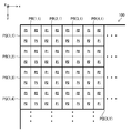
- FIG. 6 is a diagram showing a schematic configuration of an array of pixels of the image pickup device shown in FIG.
- FIG. 7 is a diagram showing a schematic configuration of the image pickup device shown in FIG. FIG.
- FIG. 8 is a cross-sectional view showing a schematic configuration of one pixel (broken line portion in FIG. 7) shown in FIG. 7.
- FIG. 9 is a diagram showing an example of an arrangement pattern of the polarizing filter elements provided in each pixel block of the image pickup device.
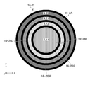
- FIG. 10 is a front view showing another embodiment of the bandpass filter unit.
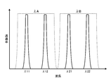
- FIG. 11 is a graph showing the transmission wavelength characteristics of each of the four bandpass filters of the bandpass filter unit shown in FIG.
- FIG. 12 is a front view of a polarizing filter unit provided corresponding to the bandpass filter unit shown in FIG.
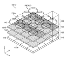
- FIG. 13 is a diagram showing a schematic configuration of another image pickup device applied to the image pickup apparatus according to the present invention.
- FIG. 14 is a cross-sectional view showing a schematic configuration of one pixel (broken line portion in FIG. 13) shown in FIG.
- FIG. 15 is a diagram showing an aberration type of an imaging optical system and variations of a bandpass filter unit corresponding to the aberration type.
- FIG. 16 is a diagram showing an aberration type of an imaging optical system and other variations of a bandpass filter unit corresponding to the aberration type.
- FIG. 17 is a diagram showing an aberration type of the imaging optical system and still another variation of the bandpass filter unit corresponding to the aberration type.
- FIG. 18 is a cross-sectional view showing an example of an imaging optical system to which the present invention is applied.
- FIG. 19 is a chart showing lens data of the imaging optical system shown in FIG. FIG.
- FIG. 20 is a front view showing the configuration of the bandpass filter unit applied to the imaging optical system shown in FIG.
- FIG. 21 is a graph showing spherical aberration, astigmatism, distortion, and chromatic aberration of magnification of the imaging optical system shown in FIG.
- FIG. 22 is a chart showing changes in axial chromatic aberration of the imaging optical system when the bandpass filter unit is not arranged and when it is arranged in the imaging optical system shown in FIG.
- FIG. 23 is a diagram used to explain the off-axis luminous flux diameter on the diaphragm.
- FIG. 24 is a diagram used to explain the presence or absence of luminous flux regulation other than the aperture.
- FIG. 21 is a graph showing spherical aberration, astigmatism, distortion, and chromatic aberration of magnification of the imaging optical system shown in FIG.
- FIG. 22 is a chart showing changes in axial chromatic aberration of the imaging optical system when the bandpass filter unit is not arranged and
- FIG. 25 is a diagram used to explain the angle of the off-axis main ray passing through the diaphragm.
- FIG. 26 is a diagram used to explain the axial marginal ray angle passing through the diaphragm.
- FIG. 27 is a diagram showing another example of the arrangement pattern of the polarizing filter element provided in each pixel block of the image pickup device.
- FIG. 28 is a diagram showing an example of one pixel of an image pickup device having a light-shielding mask.
- FIG. 29 is a flowchart showing an embodiment of the imaging method according to the present invention.
- FIG. 1 is a diagram showing a schematic configuration of an embodiment of an imaging device according to the present invention.
- the image pickup device 1 of the present embodiment is a multispectral camera that captures a first image and a second image having different wavelength bands, and includes an image pickup optical system 10, an image sensor 100, and a signal processing unit 200. ..
- the imaging optical system 10 is configured by combining a plurality of lenses 12.
- the imaging optical system 10 has a bandpass filter unit 16 and a polarizing filter unit 18 in the vicinity of the pupil thereof. Further, the imaging optical system 10 has a focus adjusting mechanism (not shown). The focus adjustment mechanism adjusts the focus by, for example, moving the entire imaging optical system 10 back and forth along the optical axis L.
- FIG. 2 is a front view showing an embodiment of the bandpass filter unit shown in FIG.
- the bandpass filter unit 16 shown in FIG. 2 has a first pupil region through which light in the first wavelength band ⁇ 1 is passed and a second pupil region through which light in a second wavelength band ⁇ 2 different from the first wavelength band is passed. It is an example of the pupil region, and functions as a wavelength selection unit that transmits light of a different wavelength band for each of the pupil regions of the first pupil region and the second pupil region.
- the bandpass filter unit 16 is arranged so that its center coincides with the optical axis L of the imaging optical system 10, and is a circular aperture region 16A1 and an aperture region divided by concentric circles centered on the optical axis L. It is composed of a frame body 16A having an outer ring-shaped opening region 16A2 of 16A1 and two wavelength selection filters (bandpass filters) 16B1 and 16B2 provided in the frame body 16A.
- one opening region 16A1 provided in the frame body 16A will be referred to as a first opening region 16A1, and the other opening region 16A2 will be referred to as a second opening region 16A2. Distinguish between 16A1 and 16A2. Further, the bandpass filter 16B1 provided in the first opening region 16A1 is referred to as a first bandpass filter 16B1, and the bandpass filter 16B2 provided in the second opening region 16A2 is referred to as a second bandpass filter 16B2. Distinguish between two bandpass filters 16B1 and 16B2.
- the frame body 16A has a light-shielding property, and the light in the first wavelength band ⁇ 1 and the first bandpass filter 16B2 are passed through the first bandpass filter 16B1 and the second bandpass filter 16B2 provided in the two opening regions 16A1 and 16A2. It transmits light in the wavelength band ⁇ 2 of 2.
- the bandpass filter unit 16 functions as a diaphragm. A diaphragm (not shown) may be provided in the imaging optical system 10, and the bandpass filter unit 16 may be installed adjacent to the diaphragm.
- the region of the first bandpass filter 16B1 (first pupil region) is larger than the region of the second bandpass filter 16B2 (second pupil region) of the imaging optical system. It is a pupil region close to the optical axis L of 10.
- FIG. 3 is a graph showing the transmission wavelength characteristics of the first bandpass filter 16B1 and the second bandpass filter 16B2, respectively.
- the first bandpass filter 16B1 transmits light in the first wavelength band ⁇ 1 and the second bandpass filter 16B2 transmits light in the second wavelength band ⁇ 2.
- the representative wavelength of the first wavelength band ⁇ 1 is shorter than the representative wavelength of the second wavelength band ⁇ 2 that passes through the second bandpass filter 16B2.
- the first bandpass filter 16B1 of the bandpass filter unit 16 transmits the light of the first wavelength band ⁇ 1 from the first pupil region near the optical axis L of the imaging optical system 10 and the second bandpass.
- the filter 16B2 transmits light in the second wavelength band ⁇ 2 from the second pupil region far from the optical axis L of the imaging optical system 10.
- the image formation position shifts toward the image plane as the distance from the optical axis of the lens increases in the peripheral direction.
- the image formation position shifts toward the object side as the distance from the optical axis of the lens increases in the peripheral direction.
- the imaging optical system 10 of this example is a lens having negative spherical aberration, and the imaging position shifts toward the object side as the distance from the optical axis of the lens increases in the peripheral direction.
- the imaging optical system 10 uses this characteristic of spherical aberration to reduce axial chromatic aberration as shown below.
- the imaging position of the light in the first wavelength band ⁇ 1 shifts to the object side from the imaging position of the light in the second wavelength band ⁇ 2.
- the image forming position of the luminous flux incident on the imaging optical system 10 shifts toward the object side as the distance from the optical axis L in the peripheral direction increases.
- a first bandpass filter 16B1 that transmits light of the first wavelength band ⁇ 1 is arranged in a circular opening region 16A1 (a region close to the optical axis L) of the frame body 16A, and a ring-shaped opening of the frame body 16A.
- the bandpass filter unit 16 is configured by arranging the second bandpass filter 16B2 that transmits light of the second wavelength band ⁇ 2 in the region 16A2 (the region far from the optical axis L).
- the imaging optical system 10 is realized in which the deviation of the imaging position due to the aberrations (1) and (2) above is canceled out and the axial chromatic aberration is satisfactorily corrected.
- the first bandpass filter 16B1 When the imaging optical system has positive spherical aberration, the first bandpass filter 16B1 has a ring-shaped shape far from the optical axis L, contrary to the bandpass filter unit 16 shown in FIG.
- the second bandpass filter 16B2 is arranged in the opening region 16A2, and the circular opening region 16A1 close to the optical axis L is arranged.
- FIG. 5 is a front view of the polarizing filter unit 18 shown in FIG.
- the polarizing filter unit 18 divides the light passing through the two pupil regions (bandpass filters 16B1 and 16B2) into pupils, and divides the light into two types of pixels (first pixel and second pixel) included in the image sensor 100. It constitutes a part of the pupil division optical system to be incident.
- the polarizing filter unit 18 is arranged so that its center coincides with the optical axis L of the imaging optical system 10, and includes the frame body 18A and the two polarizing filters 18B1 and 18B2. Consists of ,.
- the frame body 18A of the polarizing filter unit 18 has the same projected shape as the frame body 16A of the bandpass filter unit 16, and has a circular opening region 18A1 divided by concentric circles centered on the optical axis L and an annular shape. It has an opening area 18A2.
- the polarizing filter 18B1 is arranged in the circular opening region 18A1 of the frame body 18A, and the polarizing filter 18B2 is arranged in the annular opening region 18A2.
- the polarizing filter 18B1 (first polarizing filter) polarized the light passing through the first pupil region in the first direction
- the polarizing filter 18B2 (second polarizing filter) used the second pupil region.
- the light passing through is polarized in a second direction different from the first direction. That is, the directions of the polarization axes of the two polarizing filters 18B1 and 18B2 are different from each other by 90 °, and in FIG. 5, the direction of the polarization axis of the polarizing filter 18B1 is an xy plane orthogonal to the optical axis L (x axis).
- the upper left-right direction (x-axis direction), and the direction of the polarization axis of the polarizing filter 18B2 is the up-down direction (y-axis direction).
- one opening region 18A1 provided in the frame body 18A is referred to as a first opening region 18A1, and the other opening region 18A2 is referred to as a second opening region 18A2. Distinguish between 18A1 and 18A2.
- the polarizing filter 18B1 provided in the first opening region 18A1 is referred to as a first polarizing filter 18B1
- the polarizing filter 18B2 provided in the second opening region 18A2 is referred to as a second polarizing filter 18B2.
- the two polarizing filters 18B1 and 18B2 are distinguished.
- the pupil region is divided into two regions by the bandpass filter unit 16 and the polarizing filter unit 18. That is, the first pupil region defined by the first aperture region 16A1 of the bandpass filter unit 16 and the first aperture region 18A1 of the polarizing filter unit 18, and the second aperture region 16A2 of the bandpass filter unit 16 And a second pupil region defined by the second aperture region 18A2 of the polarizing filter unit 18.
- Light with different characteristics is emitted from the first pupil region and the second pupil region. That is, the first light having the first wavelength band ⁇ 1 and the polarization direction in the x direction is emitted from the first pupil region, and the second wavelength band ⁇ 2 is emitted from the second pupil region. A second light having a polarization direction of y is emitted.
- FIG. 6 is a diagram showing a schematic configuration of a pixel arrangement of the image sensor 100 shown in FIG.
- the image sensor 100 has a plurality of types (two types) of pixels P1 and P2 on the light receiving surface thereof.
- the pixels P1 and P2 are regularly arranged at a constant pitch along the horizontal direction (x-axis direction) and the vertical direction (y-axis direction).
- one pixel block PB (X, Y) is composed of four adjacent (2 ⁇ 2) pixels P1 and P2, and the pixel block PB (X, Y) is horizontal. It is regularly arranged along the direction (x-axis direction) and the vertical direction (y-axis direction).
- each pixel P1 and P2 are distinguished by using the pixel P1 as the first pixel P1 and the pixel P2 as the second pixel P2, if necessary.
- Each pixel P1 and P2 has different optical characteristics.
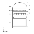
- FIG. 7 is a diagram showing a schematic configuration of the image pickup device 100 shown in FIG. 1, and FIG. 8 is a cross-sectional view showing a schematic configuration of one pixel (broken line portion in FIG. 7) shown in FIG.
- the image sensor 100 is a CMOS (Complementary Metal-Oxide Semiconductor) type image sensor, and has a pixel array layer 110, a polarizing filter element array layer 120, and a microlens array layer 140. Each layer is arranged in the order of the pixel array layer 110, the polarizing filter element array layer 120, and the microlens array layer 140 from the image plane side to the object side.
- the image sensor 100 is not limited to the CMOS type, and may be an XY address type or a CCD (Charge Coupled Device) type image sensor.
- the pixel array layer 110 is configured by arranging a large number of photodiodes 112 two-dimensionally.
- One photodiode 112 constitutes one pixel.
- Each photodiode 112 is regularly arranged along the horizontal direction (x direction) and the vertical direction (y direction).
- the polarizing filter element array layer 120 is configured by two-dimensionally arranging two types of polarizing filter elements 122A and 122B having different polarization directions (polarization directions of transmitted light).
- each polarizing filter element 122A and 122B is distinguished by using the polarizing filter element 122A as the first polarizing filter element 122A and the polarizing filter element 122B as the second polarizing filter element 122B, if necessary.
- the polarizing filter elements 122A and 122B are arranged at the same intervals as the photodiode 112, and are provided for each pixel.
- FIG. 9 is a diagram showing an example of an arrangement pattern of the polarizing filter elements provided in each pixel block of the image pickup device 100.
- the two polarizing filters 18B1 and 18B2 are different from each other in the direction of the polarization axis by 90 °, and the direction of the polarization axis of the first polarization filter element 122A (first polarization direction ⁇ 1) is shown in FIG.
- the direction of the polarization axis of the second polarizing filter 18B2 is the vertical direction (y-axis direction).
- the polarizing filter elements 122A and 122B are regularly arranged.
- the first polarization direction ⁇ 1 of the first polarization filter element 122A coincides with the polarization direction of the first polarization filter 18B1 of the polarization filter unit 18 (FIG. 5), and the second polarization of the second polarization filter element 122B.
- the direction ⁇ 2 coincides with the polarization direction of the second polarizing filter 18B2 of the polarizing filter unit 18.
- the first pixel P1 having the polarizing filter element 122A of the imaging element 100 receives only the first light of the first wavelength band ⁇ 1 transmitted through the first pupil region having the first polarizing filter 18B1.
- the second pixel P2 having the polarizing filter element 122B receives only the second light of the second wavelength band ⁇ 2 transmitted through the second pupil region having the second polarizing filter 18B2.
- the image pickup device 1 When the image pickup device 1 receives a shooting instruction input from a shutter release switch or the like, the image pickup device 1 performs exposure control on the image sensor 100.
- the optical image of the subject imaged on the light receiving surface of the image sensor 100 by this exposure control is converted into an electric signal by the image sensor 100.
- Charges corresponding to the amount of light incident on the photodiode 112 are accumulated in each pixel (first pixel, second pixel) of the image sensor 100, and the amount of charge accumulated in each pixel from the image sensor 100.
- the electric signal corresponding to the above is read out as an image signal and output.
- the signal processing unit 200 processes the signal output from the image sensor 100, and based on the output signal of the first pixel P1 and the output signal of the second pixel P2, the first wavelength band ⁇ 1 A first image of the above and a second image of the second wavelength band ⁇ 2 are generated, respectively.
- the image pickup apparatus 1 can simultaneously capture the first image of the first wavelength band ⁇ 1 and the second image (multispectral image) of the second wavelength band ⁇ 2, and the first image and the first image and The second image is an image having different wavelength bands from each other, but is captured as an image in which the axial chromatic aberration of the imaging optical system 10 is improved.
- FIG. 10 is a front view showing another embodiment of the bandpass filter unit.
- the bandpass filter unit 16-2 shown in FIG. 10 has a first pupil region through which light in the first wavelength band ⁇ 11 passes, a second pupil region through which light in the second wavelength band ⁇ 12 passes, and a second pupil region.
- This is an example of a third pupil region through which light in the wavelength band ⁇ 21 passes and a fourth pupil region in which light in the fourth wavelength band ⁇ 22 passes, and is a pupil region from the first pupil region to the fourth pupil region. It functions as a wavelength selection unit that transmits light in different wavelength bands.
- the bandpass filter unit 16-2 is arranged so that its center coincides with the optical axis of the imaging optical system, and has a circular aperture region divided by concentric circles centered on the optical axis and three ring-shaped aperture regions. 16-2A and the first wavelength selection filter to the fourth wavelength selection filter (four bandpass filters) 16-2B1 to 16-2B4 provided in the frame body 16-2A. Will be done.
- FIG. 11 is a graph showing the transmission wavelength characteristics of each of the four bandpass filters 16-2B1 to 16-2B4 of the bandpass filter unit 16-2 shown in FIG.
- the bandpass filter 16-2B1 transmits light in the first wavelength band ⁇ 11
- the bandpass filter 16-2B2 transmits light in the second wavelength band ⁇ 12
- the bandpass filter 16-2B3 transmits light in the second wavelength band ⁇ 12.
- the bandpass filter 16-2B4 transmits the light of the wavelength band ⁇ 21 of the above, and transmits the light of the fourth wavelength band ⁇ 22.
- the second wavelength band ⁇ 12, the third wavelength band ⁇ 21, and the fourth wavelength band in which the representative wavelengths are sequentially lengthened are provided in the three ring-shaped pupil regions in which the pass filter 16-2B1 is arranged and sequentially moves away from the optical axis.
- Bandpass filters 16-2B2 to 16-2B4 that transmit the light of ⁇ 22 are arranged.
- An imaging optical system capable of satisfactorily correcting axial chromatic aberration is configured by canceling the deviation of the imaging position due to axial chromatic aberration by the deviation of the imaging position due to spherical aberration.
- FIG. 12 is a front view of the polarizing filter unit 18-2 provided corresponding to the bandpass filter unit 16-2 shown in FIG.
- the polarizing filter unit 18-2 divides the light passing through the four pupil regions (bandpass filters 16-2B1 to 16-2B4) into pupils, and divides the light into four types of pixels (first) included in the image sensor 100-2. It constitutes a part of the pupil division optical system that is incident on the pixels (pixels to the fourth pixel).
- the polarizing filter unit 18-2 is arranged so that its center coincides with the optical axis of the imaging optical system.
- the frame body 18-2A and the four polarizing filters It is composed of 18-2B1 to 18-2B4.
- the frame 18-2A of the polarizing filter unit 18-2 has the same projected shape as the frame 16-2A of the bandpass filter unit 16-2, and is a circular opening divided by concentric circles centered on the optical axis. It has a region and three ring-shaped opening regions.
- the polarizing filter 18-2B1 is arranged in the circular opening region of the frame body 18-2A, and the three polarizing filters 18-2B2 to 18-2B4 are arranged in the three ring-shaped opening regions, respectively.
- the polarization axes of the two polarization filters 18-2B1 and 18-2B3 out of the four polarization filters 18-2B1 to 18B4 are in the left-right direction (x-axis direction) on FIG. 12, and the remaining two polarizations.
- the polarization axes of the filters 18-2B3 and 18-2B4 are in the vertical direction (y-axis direction) on FIG. 12, and the polarizing filters 18-2B1 and 18-2B3 and the polarizing filters 18-2B3 and 18-2B4 are mutually exclusive.
- the directions of the polarization axes are different by 90 °.
- the bandpass filter unit 16-2 shown in FIG. 10 transmits light of four wavelength bands ⁇ 11, ⁇ 12, ⁇ 21, and ⁇ 22 from four pupil regions, respectively, and transmits light of four wavelength bands ⁇ 11, ⁇ 12, ⁇ 21, and ⁇ 22, respectively. Is emitted by the polarizing filter unit 18-2 as the first light in the wavelength bands ⁇ 11 and ⁇ 21 in the x direction in the polarization direction and the second light in the wavelength bands ⁇ 12 and ⁇ 22 in the y direction in the polarization direction.
- FIG. 13 is a diagram showing a schematic configuration of another image pickup device applied to the image pickup device according to the present invention.
- FIG. 14 is a cross-sectional view showing a schematic configuration of one pixel (broken line portion in FIG. 13) shown in FIG.
- the same reference numerals are given to the parts common to the image pickup devices shown in FIGS. 7 and 8, and detailed description thereof will be omitted.
- the image pickup device 100-2 shown in FIGS. 13 and 14 has the addition of a spectroscopic filter element array layer 130 functioning as a first wavelength selection filter and a second wavelength selection filter. It is different from the element 100.
- the spectroscopic filter element array layer 130 is configured by two-dimensionally arranging two types of spectroscopic filter elements 132A and 132B (first wavelength selection filter and second wavelength selection filter) having different transmission wavelength characteristics from each other.
- each spectroscopic filter element 132A and 132B will be distinguished by using the spectroscopic filter element 132A as the first spectroscopic filter element 132A and the spectroscopic filter element 132B as the second spectroscopic filter element 132B, if necessary.
- the spectroscopic filter elements 132A and 132B are arranged at the same intervals as the photodiode 112, and are provided for each pixel.
- FIG. 11 is a graph including an example of transmission wavelength characteristics of each spectroscopic filter element.
- the first spectroscopic filter element 132A transmits light in the wavelength band ⁇ A
- the second spectroscopic filter element 132B transmits light in the wavelength band ⁇ B.
- the first light in the wavelength bands ⁇ 11 and ⁇ 21 whose polarization direction is the x direction and the second light in the wavelength bands ⁇ 12 and ⁇ 22 whose polarization direction is the y direction are incident on the image pickup element 100-2.
- the pixel having the first spectral filter element 132A and the first polarizing filter element 122A is defined as the pixel P1
- the first spectral filter element 132A and the second polarizing filter element A pixel having 122B is a pixel P2
- a pixel having a second spectral filter element 132B and a first polarizing filter element 122A is a pixel P3
- a pixel having a second spectral filter element 132B and a second polarizing filter element 122B is defined as the pixel P1
- the first spectral filter element 132A and the second polarizing filter element A pixel having 122B is a pixel P2
- a pixel having a second spectral filter element 132B and a first polarizing filter element 122A is a pixel P3
- a pixel having a second spectral filter element 132B and a second polarizing filter element 122B is defined as the pixel P1
- one pixel block PB (X, Y) is composed of four adjacent (2 ⁇ 2) pixels P1, P2, P3, and P4, and this pixel block PB (X, Y) is formed.
- PBs (X, Y) are regularly arranged along the horizontal direction (x-axis direction) and the vertical direction (y-axis direction).
- pixels P1, P2, P3, and P4 are referred to as first pixel P1, second pixel P2, third pixel P3, and fourth pixel P4, and four types of pixels P1, P2, P3, and P4 are referred to as four types. Pixels P1, P2, P3, P4 are distinguished.
- the four types of pixels P1 to P4 are composed of polarizing filter elements 122A and 122B, and spectroscopic filter elements 132A. With the combination of 132B, only light in any one of the four wavelength bands ⁇ 11 to ⁇ 22 is received. That is, the first pixel P1 receives only the light in the wavelength band ⁇ 11, the second pixel P2 receives only the light in the wavelength band ⁇ 12, and the third pixel P3 receives only the light in the wavelength band ⁇ 21. Upon receiving light, the fourth pixel P4 receives only light in the wavelength band ⁇ 22.
- the image pickup device When the image pickup device receives a shooting instruction input from a shutter release switch or the like, the image pickup device performs exposure control on the image pickup element 100-2.
- the optical image of the subject imaged on the light receiving surface of the image sensor 100-2 by this exposure control is converted into an electric signal by the image sensor 100-2.
- an electric charge corresponding to the amount of light incident on the photodiode 112 is accumulated, and from the image sensor 100-2, the electric charge accumulated in each pixel is accumulated.
- the corresponding electric signal is read out as an image signal and output.
- the signal processing unit 200 shown in FIG. 1 processes the signal output from the image pickup element 100-2, and outputs the output signal of the first pixel P1, the output signal of the second pixel P2, and the output signal of the third pixel P3. , And a first image of the first wavelength band ⁇ 11, a second image of the second wavelength band ⁇ 12, a third image of the third wavelength band ⁇ 21, and a third image of the third wavelength band ⁇ 21, based on the output signal of the fourth pixel P4. A fourth image of the fourth wavelength band ⁇ 22 is generated, respectively.
- the image pickup apparatus can use the first image of the first wavelength band ⁇ 11, the second image of the second wavelength band ⁇ 12, the third image of the third wavelength band ⁇ 21, and the fourth wavelength band ⁇ 22.
- the fourth image (multispectral image) can be simultaneously imaged, and the first to fourth images have different wavelength bands from each other, but the axial chromatic aberration of the imaging optical system is improved. It is imaged as an image.
- [Variations of bandpass filter units corresponding to the aberration type of the imaging optical system] 15 to 17 are diagrams showing an aberration type of the imaging optical system and variations of the bandpass filter unit corresponding to the aberration type, respectively.
- Spherical aberration, coma, and astigmatism can be considered as the aberration types of the imaging optical system that can be applied to correct the axial chromatic aberration of the imaging optical system.
- the imaging optical system may be designed so that aberrations other than the axial chromatic aberration of the imaging optical system are positively generated.
- spherical aberration is generated by changing the surface spacing or curvature near the aperture for an imaging optical system in which spherical aberration is well corrected. It is possible to make it.
- coma is generated by eccentricity of a lens near the diaphragm, and as a method of realizing an imaging optical system having astigmatism, it is near the diaphragm. It is conceivable to generate astigmatism by arranging the anamorphic lens.
- the imaging position shifts depending on the position of the pupil.
- the regions a1, b1 and c1 are a region in which the phase advances with respect to the region b1 in the imaging optical system and the region c1 is a region c1 in which the phase is delayed, the regions a1, b1 and c1 The imaging position approaches the image plane side in order.
- Bandpass filters having different wavelength bands are assigned to each of the corresponding pupil regions a2, b2, and c2. That is, a bandpass filter having a long wavelength that transmits in the order of regions a2, b2, and c2 is arranged.
- bandpass filters having different transmission wavelength bands are appropriately arranged corresponding to (B) “wavelength allocation image” in FIG. 15, the deviation of the imaging position due to the influences of 1) and 2) cancel each other out. It is possible to realize an imaging optical system in which axial chromatic aberration is satisfactorily corrected.
- FIG. 15 (C) “concentric circle type”
- FIG. 15 (D) “circular opening vertical 3-hole type”
- FIG. E "Circular opening cross 5 hole type”
- FIG. 16 (F) “Circular opening vertical 5 hole type”
- FIG. 16 (G) “Circular opening cross 9 hole type”
- FIG. 16 (H) “Circular”
- the six bandpass filter units shown in “Opening 8 directions 9 holes type" are shown in FIGS. 15 and 16.
- the imaging optical system having spherical aberration has the characteristic (characteristic of negative spherical aberration) shown in (A) “aberration characteristic” of FIG. 15, in order to correct the axial chromatic aberration, (B) of FIG.
- a bandpass filter having a long wavelength that transmits in the order of regions a2, b2, and c2 that are sequentially moved away from the optical axis is arranged.
- the "concentric circle type" in FIG. 15 (C) is a bandpass filter unit of the same type as the bandpass filter unit 16 shown in FIG. 2 and the bandpass filter unit 16-2 shown in FIG.
- the filter unit has a visible white filter in a circular aperture on the optical axis or a circular aperture without a filter, and a plurality of circular apertures separated by an equal distance from the optical axis have a representative wavelength higher than that of the visible white representative wavelength.
- a bandpass filter that transmits light in a long wavelength band is arranged.
- an image in the visible white wavelength band and an image in a wavelength band having a longer representative wavelength than the visible white representative wavelength can be simultaneously captured, and each image having a different wavelength band can be captured at the same time. Even so, the focusing accuracy of each image can be improved.
- (F) “circular opening vertical 5-hole type” of FIG. 16 and (G) “circular opening cross 9-hole type” of FIG. 16 (E) of FIG. 15 have a first wavelength band having a short wavelength in the center.
- a bandpass filter that transmits light is arranged, and a bandpass filter that transmits light in a second wavelength band having a long wavelength is arranged in the outermost part, and an intermediate between the first wavelength band and the second wavelength band is arranged in the middle. It has a third pupil region through which light in the third wavelength band of the above is passed.
- bandpass filter units when the spherical aberration is negative, a bandpass filter having a longer wavelength is arranged as the distance from the optical axis increases. In this way, by arranging the bandpass fill for each wavelength band in consideration of the spherical aberration of the imaging optical system, the deviation of the imaging position for each wavelength due to the axial chromatic aberration is reduced, and a plurality of images are simultaneously imaged. I am trying to improve the focusing accuracy of the image.
- the light is transmitted in the order of regions gradually moving away from the optical axis. Place a bandpass filter with a short wavelength.
- FIG. 15 (D) “circular opening vertical 3-hole type”
- FIG. 15 (E) “circular opening cross 5-hole type”
- 16 (F) “Circular opening vertical 5 hole type”
- FIG. 16 (G) “Circular opening cross 9 hole type”
- FIG. 16 (H) “Circular opening 8 direction 9 hole type”
- FIG. J) "Square opening 2x2 type”
- FIG. 17 (K) Square opening 8-hole rhombic type
- FIG. 17 (L) “Square opening 3x3 type", FIG.
- the imaging position on the optical axis of the light incident on the region a2 of the (first region) and the region c2 (second region) moves to the image side, and is on the optical axis of the light incident on the region c2.
- the imaging position moves to the object side.
- the bandpass filter unit that reduces axial chromatic aberration by utilizing coma has three circular openings from bottom to top in FIG. Bandpass filters that transmit longer wavelengths are sequentially arranged.
- the imaging position shifts toward the object from the bottom to the top due to the influence of coma, but the wavelength gradually shifts from the bottom to the top.
- a bandpass filter unit having a long bandpass filter it is possible to cancel the deviation of the imaging position due to axial chromatic aberration and obtain a good image in which the deviation of the imaging position for each wavelength is reduced. ..
- a bandpass filter in which the transmitted wavelength becomes longer is sequentially arranged in each opening from the bottom to the top.
- the 10 bandpass filter units shown in the “divided type” and the “fan-shaped 8-divided type” in FIG. 17 (O) are shown in FIGS. 15 to 17.
- the imaging optical system having astigmatism has the characteristics shown in (A) "abrasive characteristics" of FIG. 15, it is incident on the left and right regions (first region) symmetrical with respect to the optical axis of the imaging optical system.
- the imaging position on the optical axis of light moves to the image side, and it is an upper and lower region (second region) symmetrical with respect to the optical axis and is orthogonal to the left and right regions (including the case where it is substantially orthogonal).
- the imaging position on the optical axis of the light incident on the upper and lower regions moves to the object side.
- the bandpass filter unit that reduces axial chromatic aberration by utilizing non-point aberration has a circular aperture in the center (on the optical axis) in FIG.
- the left and right circular openings are arranged with short wavelength bandpass filters
- the upper and lower circular openings are arranged with short wavelength bandpass filters.
- bandpass filters having shorter wavelengths transmitted are sequentially arranged as the distance from the center in the left-right direction is shorter than that of the center bandpass filter, while the center.
- a bandpass filter having a longer transmitted wavelength is sequentially arranged than the central bandpass filter as the distance from the bandpass filter increases in the vertical direction.
- band pass filter In the case of (I) "circular aperture astigmatism special type" of FIG. 16, a band pass filter is not arranged in the center, and light is emitted to the 12 circular openings formed along the sides of the substantially rhombus. Bandpass filters with shorter transmitted wavelengths are sequentially arranged as they move away from the straight line in the vertical direction passing through the axis in the horizontal direction.
- the bandpass filter unit shown in (J) “square opening 2x2 type” in FIG. 16 and (N) “fan-shaped 4-split type” in FIG. 17 has a visible white filter in the left and right openings or an opening without a filter. Bandpass filters that transmit light in a wavelength band whose representative wavelength is longer than the representative wavelength of visible white are arranged in the upper and lower openings.
- a bandpass filter in which the transmitted wavelength becomes shorter as the distance from the left and right direction increases is arranged, and a bandpass filter in which the transmitted wavelength becomes longer as the distance from the vertical direction increases.
- the wavelength to be transmitted depends on the characteristic of the astigmatism. It is necessary to determine the position and area of multiple bandpass filters with different wavelengths.
- FIG. 18 is a cross-sectional view showing an example of an imaging optical system to which the present invention is applied.
- the imaging optical system 20 shown in FIG. 18 includes a front group lens 20A arranged on the object side of the aperture position indicated by the surface number 8 and a rear group lens 20B arranged on the image side of the aperture position. Have.
- 1 to 7 indicate surface numbers for the four lenses constituting the front group lens 20A
- 9 to 16 indicate surface numbers for the four lenses constituting the rear group lens 20B and the parallel flat plate. ing.
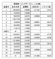
- FIG. 19 is a chart showing the lens data of the imaging optical system 20 shown in FIG.
- FIG. 20 is a front view showing the configuration of the bandpass filter unit applied to the imaging optical system 20 shown in FIG.
- the bandpass filter unit 16-3 shown in FIG. 20 is arranged between the front group lens 20A and the rear group lens 20B of the imaging optical system 20 shown in FIG. 18, for example, at the position of the aperture shown in FIG. It is placed and can function as a fixed diaphragm or can be placed adjacent to the diaphragm.
- the bandpass filter unit 16-3 is a "concentric circle type" bandpass filter unit equivalent to the bandpass filter unit 16-2 shown in FIG. 10, and has diameters of 6 mm, 6 ⁇ 2 mm, 6 ⁇ 3 mm, and 12 mm, respectively.
- a pass filter, a bandpass filter that transmits a representative wavelength ⁇ 21 (red: 668 nm), and a bandpass filter that transmits a representative wavelength ⁇ 22 (red edge: 717 nm) are arranged and configured.
- the imaging optical system 20 of this embodiment has a polarizing filter unit (corresponding to the polarizing filter unit 18-2 shown in FIG. 12) corresponding to the bandpass filter unit 16-3.
- FIG. 21 is a graph showing spherical aberration, astigmatism, distortion, and chromatic aberration of magnification of the imaging optical system 20 shown in FIG.
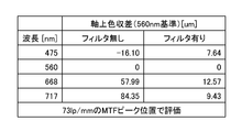
- FIG. 22 is a chart showing changes in the axial chromatic aberration of the imaging optical system 20 when the bandpass filter unit 16-3 is not arranged in the imaging optical system 20 and when it is arranged.
- the axial chromatic aberration shown in FIG. 22 indicates the amount of deviation of the imaging position of another wavelength with respect to the wavelength ⁇ 12 (60 nm), and the negative value indicates the amount of deviation toward the object side. Further, these deviation amounts were measured based on the imaging position where the MFT (Modulation Transfer Function) at the spatial frequency 73 [lp / mm] takes a peak value.
- MFT Modulation Transfer Function
- n be an integer of 2 or more
- i be a parameter that changes in the range of 1 to n
- ⁇ i be the i-th pupil region of the imaging optical system.
- ⁇ ij be the representative wavelength of light transmitted through the i-th pupil region ⁇ i.
- the m i be the number of the representative wavelength in the pupil region ⁇ i of the i
- j be a parameter that changes in the range of 1 to m.
- ⁇ ij be the j-th representative wavelength in the i-th pupil region ⁇ i.
- f ( ⁇ ) be the paraxial focal length at the wavelength ⁇ of the imaging optical system.
- g (x, y; ⁇ ) be the axial longitudinal aberration of the wavelength ⁇ at the pupil coordinates (x, y) of the pupil region of the imaging optical system.
- S ⁇ i be the area of the third pupil region ⁇ i.
- the imaging optical system is based on the following [Equation 1] and [Equation 2] equations.
- Equation 1 means that the imaging optical system has axial chromatic aberration exceeding a.
- Equation 2 is preferably b ⁇ 8p.
- the depth of focus of the imaging optical system can be expressed as ⁇ ⁇ F, where ⁇ is the permissible circle of confusion diameter and F is the aperture value (F value).
- F the aperture value
- the axial chromatic aberration of the imaging optical system can be reduced within the depth of focus of the imaging optical system.
- the permissible circle of confusion diameter ⁇ is a full Nyquist of the pixel pitch p of the image sensor, and b ⁇ 4p.
- the axial chromatic aberration with a filter shown in FIG. 22 satisfies b ⁇ 4p.
- FIG. 23 is a diagram used to explain the off-axis luminous flux diameter on the diaphragm.
- the image of the wavelength assigned to the outermost outline does not show the periphery with a high image height as shown in FIG. 23 (B). That is, the image circle becomes smaller.
- an imaging optical system having a large image circle is used so that the off-axis luminous flux can cover the outermost ring-shaped region, and as shown in FIG. 23 (C), the image of the wavelength assigned to the outermost shell is also the outermost periphery. It is preferable to capture up to.
- FIG. 24 is a diagram used to explain the presence or absence of luminous flux regulation other than the aperture.
- FIG. 24 (A) is a diagram showing an imaging optical system 30-1 in which the luminous flux is regulated by the diaphragm 32
- FIG. 24 (B) is a diagram showing an imaging optical system 30-2 in which the luminous flux is regulated by other than the diaphragm 32.
- the off-axis luminous flux diameter on the diaphragm 32 can cover almost the entire area of the diaphragm 32, and it is possible to cover each ring-shaped region (for each wavelength band).
- the image size can be the same.
- FIG. 25 is a diagram used to explain the angle of the off-axis main ray passing through the diaphragm.
- the imaging optical system 40 shown in FIG. 25 has a front group lens 40A and a rear group lens 40B, and an aperture surface 42 is located between the front group lens 40A and the rear group lens 40B.
- the angle ⁇ of the off-axis main ray passing through the diaphragm surface 42 is determined by the angle of the ray and the angular magnification of the front lens group lens 40A.
- the angle ⁇ of the off-axis main ray passing through the diaphragm surface 42 approaches perpendicular to the diaphragm surface 42.
- the input angle of light incident on the diaphragm surface 42 or the bandpass filter (not shown) arranged adjacent to the diaphragm surface 42 can be reduced, and the wavelength shift due to the large incident angle is reduced. can do.
- FIG. 26 is a diagram used to explain the axial marginal ray angle passing through the diaphragm.
- the imaging optical system 50 shown in FIG. 26 has a front group lens 50A and a rear group lens 50B, and an aperture surface 52 is located between the front group lens 50A and the rear group lens 50B.
- the axial marginal ray angle ⁇ passing through the diaphragm surface 52 is determined by the entrance pupil diameter and the focal length of the front lens group lens 50A.
- the front group lens 50A has a focal length that brings the on-axis marginal ray angle ⁇ incident on the diaphragm surface 52 closer to perpendicular to the diaphragm surface 52.
- the axial marginal ray angle ⁇ passing through the diaphragm surface 52 approaches perpendicular to the diaphragm surface 52.
- the axial marginal ray angle ⁇ (input angle) incident on the diaphragm surface 52 or the bandpass filter (not shown) arranged adjacent to the diaphragm surface 52 can be reduced, and the incident angle becomes large. This makes it possible to reduce the wavelength shift.
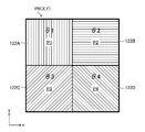
- FIG. 27 is a diagram showing another example of the arrangement pattern of the polarizing filter element provided in each pixel block of the image pickup device.
- the four pixels P1 to P4 constituting one pixel block PB are provided with polarizing filter elements 122A to 122D having different transmission polarization directions.
- the first pixel P1 is provided with a polarizing filter element 122A (first polarizing filter) that transmits light in the polarization direction ⁇ 1 (for example, 90 °).
- the second pixel P2 is provided with a second polarizing filter element 122B (second polarizing filter) that transmits light in the polarization direction ⁇ 2 (for example, 0 °).
- the third pixel P3 is provided with a third polarizing filter element 122C (third polarizing filter) that transmits light in the polarization direction ⁇ 3 (for example, 45 °).
- the fourth pixel P4 is provided with a fourth polarizing filter element 122D (fourth polarizing filter) that transmits light in the polarization direction ⁇ 4 (for example, 135 °).
- the number of wavelength bands selected by the bandpass filter unit is three, and three types of polarization filter units (for example, ⁇ 1, ⁇ 2, ⁇ 3) are arranged corresponding to each pupil region of the bandpass filter unit. It is assumed that it has been done.
- the signal processing unit 200 (FIG. 1) performs interference removal processing to generate an image signal in each wavelength band.
- the pixel signal (signal value) obtained from the first pixel P1 of each pixel block PB (X, Y) is x1
- the pixel signal obtained from the second pixel P2 is x2
- the signal processing unit 200 calculates three pixel signals X1 to X3 corresponding to light in each wavelength band (for example, ⁇ 1, ⁇ 2, ⁇ 3) from the three pixel signals x1 to x3, and eliminates interference.
- the three pixel signals X1 to X3 corresponding to the light of each wavelength band ⁇ 1, ⁇ 2, and ⁇ 3 are calculated by the [Equation 4] equation using the matrix A of the [Equation 3] equation, and the interference is eliminated. To do.
- Interference occurs when light from the pupil region of each wavelength band is mixed into each pixel P1 to P3.
- the ratio of light incident on the pupil region of each wavelength band received by each pixel P1 to P3 (the amount of interference (also referred to as the interference ratio)) is the polarization direction of the polarizing filter unit provided in the pupil region of each wavelength band. It is uniquely determined from the relationship between the above and the polarization directions of the polarizing filter elements 122A to 122C provided in the pixels P1 to P3.
- the ratio of light incident on the first pupil region received by the first pixel P1 (interference amount) is b11, and the ratio of light incident on the second pupil region is received by the first pixel P1.
- the ratio of light incident on b12 and the third pupil region received by the first pixel P1 is b13, the following relationship holds between X1, X2, X3 and x1.
- X1, X2, and X3 are calculated by the following equation by multiplying both sides of the equation [Equation 9] by the inverse matrix B -1 of the matrix B.
- the pixel signals X1, X2, and X3 of the image obtained in each pupil region are each pixel P1 based on the ratio (interference amount) that the light incident on each pupil region is received by each pixel P1 to P3. It can be calculated from the pixel signals x1, x2, x3 of P3.
- a first microlens and a first light-shielding mask having a first aperture corresponding to a first pupil region are arranged in the first pixel of the image sensor, and a second microlens is placed in the second pixel of the image sensor. And a second shading mask with a second aperture corresponding to the second pupil region is placed.
- the first pupil region and the second pupil region are divided by using the light-shielding mask (first light-shielding mask, second light-shielding mask), and the first pixel and the second pixel of the image pickup device are divided.
- a light beam passing through each pupil region can be incident on the surface.
- FIG. 28 is a diagram showing an example of one pixel of an image pickup device having a light-shielding mask.
- 112 is a photodiode
- 142 is a microlens
- the light-shielding mask M is arranged between the photodiode 112 and the microlens 142.
- the light-shielding mask M has an opening corresponding to the shape of each pupil region.
- the photodiode 112 receives only the light passing through the desired pupil region by the light-shielding mask M.
- the pixel block of the image pickup device by configuring the pixel block of the image pickup device with a plurality of types of pixels provided with a light-shielding mask M having an aperture corresponding to the shape of each pupil region, an image of each wavelength band passing through each pupil region is acquired. can do.
- FIG. 29 is a flowchart showing an embodiment of the imaging method according to the present invention.
- the imaging method shown in FIG. 29 corresponds to the imaging device 1 shown in FIG. 1, and when carrying out this imaging method, the imaging optical system 10 according to the present invention is prepared.
- the image pickup apparatus 1 determines whether or not there is an instruction input for taking an image of a plurality of wavelength bands by, for example, an instruction input from a shutter release switch (step S10).
- the image pickup device 1 controls the exposure to the image pickup device 100 when it receives an input of a shooting instruction (step S12). As a result, electric charges corresponding to the amount of light incident on the photodiode are accumulated in each pixel (first pixel P1 and second pixel P2) of the image sensor 100, and are accumulated in each pixel from the image sensor 100. An electric signal corresponding to the amount of electric charge is read out as an image signal and output.
- the signal processing unit 200 acquires a signal output from the image sensor 100 (step S14), generates a first image in the first wavelength band based on the output signal of the first pixel P1, and second. A second image of the second wavelength band ⁇ 2 is generated based on the output signal of the pixel P2.
- the image pickup apparatus 1 can simultaneously capture the first image of the first wavelength band ⁇ 1 and the second image (multispectral image) of the second wavelength band ⁇ 2, and the first image and the first image and The second image is an image in which the wavelength bands differ from each other due to the bandpass filter unit 16, but the axial chromatic aberration of the imaging optical system 10 due to the difference between the first wavelength band ⁇ 1 and the second wavelength band ⁇ 2 is captured.
- Imaging optics that reduce based on the relationship between aberrations other than axial chromatic aberration of the optical system 10 (spherical aberration in the embodiment of FIG. 1) and the positions of the first pupil region and the second pupil region of the imaging optical system 10. Since it is the system 10, it is captured as a multispectral image with improved axial chromatic aberration.
- the imaging apparatus is not limited to capturing still images in a plurality of wavelength bands, and may capture moving images in a plurality of wavelength bands at the same time.
- the present invention is not limited to the image pickup apparatus, and includes an image pickup optical system constituting the image pickup apparatus.
- an imaging device in which the imaging optical system can be exchanged, it is possible to acquire a multispectral image in a desired wavelength band by exchanging with an imaging optical system designed according to the wavelength band.
- Imaging device 10 20, 30-1, 30-2, 40, 50 Imaging optical system 11A, 11B Restriction point 12 Lens 16, 16-2, 16-3, 16-4 Bandpass filter unit 16A, 16-2A , 18A, 18-2A Frame 16B1, 16B2, 16-2B1, 16-2B2, 16-2B3, 16-2B4 Bandpass filter 16A1, 16A2, 18A1, 18A2 Opening area 18, 18-2 Polarized filter unit 18B1, 18B2 , 18-2B1, 18-2B2, 18-2B3 Polarizing filter 20A, 40A, 50A Front group lens 20B, 40B, 50B Rear group lens 32 Aperture 42, 52 Aperture surface 100, 100-2 Imaging element 110 Pixel array layer 112 Photo Diode 120 Polarized filter element Array layer 122A, 122B, 122C, 122D Polarized filter element 130 Spectral filter element Array layer 132A, 132B Spectral filter element 140 Microlens Array layer 142 Microlens 200 Signal processing unit L Optical axis M Shading mask P1, P2
Landscapes
- Physics & Mathematics (AREA)
- General Physics & Mathematics (AREA)
- Optics & Photonics (AREA)
- Spectroscopy & Molecular Physics (AREA)
- Engineering & Computer Science (AREA)
- Signal Processing (AREA)
- Multimedia (AREA)
- Studio Devices (AREA)
- Lenses (AREA)
- Spectrometry And Color Measurement (AREA)
- Optical Filters (AREA)
- Polarising Elements (AREA)
- Color Television Image Signal Generators (AREA)
Priority Applications (3)
| Application Number | Priority Date | Filing Date | Title |
|---|---|---|---|
| JP2021553594A JP7220302B2 (ja) | 2019-10-30 | 2020-10-26 | 撮像装置、撮像光学系及び撮像方法 |
| CN202080075588.0A CN114631057B (zh) | 2019-10-30 | 2020-10-26 | 摄像装置、摄像光学系统及摄像方法 |
| US17/721,330 US11930256B2 (en) | 2019-10-30 | 2022-04-14 | Imaging device, imaging optical system, and imaging method |
Applications Claiming Priority (2)
| Application Number | Priority Date | Filing Date | Title |
|---|---|---|---|
| JP2019197778 | 2019-10-30 | ||
| JP2019-197778 | 2019-10-30 |
Related Child Applications (1)
| Application Number | Title | Priority Date | Filing Date |
|---|---|---|---|
| US17/721,330 Continuation US11930256B2 (en) | 2019-10-30 | 2022-04-14 | Imaging device, imaging optical system, and imaging method |
Publications (1)
| Publication Number | Publication Date |
|---|---|
| WO2021085368A1 true WO2021085368A1 (ja) | 2021-05-06 |
Family
ID=75715161
Family Applications (1)
| Application Number | Title | Priority Date | Filing Date |
|---|---|---|---|
| PCT/JP2020/040065 Ceased WO2021085368A1 (ja) | 2019-10-30 | 2020-10-26 | 撮像装置、撮像光学系及び撮像方法 |
Country Status (4)
| Country | Link |
|---|---|
| US (1) | US11930256B2 (https=) |
| JP (1) | JP7220302B2 (https=) |
| CN (1) | CN114631057B (https=) |
| WO (1) | WO2021085368A1 (https=) |
Cited By (1)
| Publication number | Priority date | Publication date | Assignee | Title |
|---|---|---|---|---|
| US12181663B2 (en) * | 2020-07-28 | 2024-12-31 | Fujifilm Corporation | Imaging device, adjustment method, and adjustment program |
Families Citing this family (3)
| Publication number | Priority date | Publication date | Assignee | Title |
|---|---|---|---|---|
| US11853845B2 (en) * | 2020-09-02 | 2023-12-26 | Cognex Corporation | Machine vision system and method with multi-aperture optics assembly |
| JP2023173099A (ja) * | 2022-05-25 | 2023-12-07 | キヤノン株式会社 | 検査装置 |
| FR3143777A1 (fr) * | 2022-12-19 | 2024-06-21 | Thales | Dispositif de filtrage à effet variable |
Citations (3)
| Publication number | Priority date | Publication date | Assignee | Title |
|---|---|---|---|---|
| JP2004157059A (ja) * | 2002-11-08 | 2004-06-03 | Minolta Co Ltd | 撮像装置およびレンズ光学系 |
| WO2012043211A1 (ja) * | 2010-10-01 | 2012-04-05 | 富士フイルム株式会社 | 撮像装置 |
| WO2014020791A1 (ja) * | 2012-08-02 | 2014-02-06 | パナソニック株式会社 | 偏光カラー撮像装置 |
Family Cites Families (11)
| Publication number | Priority date | Publication date | Assignee | Title |
|---|---|---|---|---|
| JPH10170816A (ja) * | 1996-12-09 | 1998-06-26 | Canon Inc | ピント合わせ情報検出装置及び焦点検出装置及びそれを用いたカメラ |
| JP5610254B2 (ja) * | 2008-06-18 | 2014-10-22 | 株式会社リコー | 撮像装置及び路面状態判別方法 |
| WO2012111220A1 (ja) * | 2011-02-15 | 2012-08-23 | 富士フイルム株式会社 | 撮像装置、撮像装置本体およびシェーディング補正方法 |
| EP2536153B1 (en) * | 2011-04-22 | 2016-04-13 | Panasonic Intellectual Property Management Co., Ltd. | Image capture device, image capture system, and image capture method |
| CN103119516B (zh) * | 2011-09-20 | 2016-09-07 | 松下知识产权经营株式会社 | 光场摄像装置和图像处理装置 |
| US9658463B2 (en) * | 2012-02-03 | 2017-05-23 | Panasonic Intellectual Property Management Co., Ltd. | Imaging device and imaging system |
| US9395516B2 (en) * | 2012-05-28 | 2016-07-19 | Nikon Corporation | Imaging device |
| US9509893B2 (en) * | 2014-03-31 | 2016-11-29 | Panasonic Intellectual Property Management Co., Ltd. | Imaging device and analyzing apparatus using the imaging device |
| GB2548462B (en) * | 2016-01-29 | 2020-06-17 | Canon Kk | Image sensor and image capturing apparatus |
| EP3697075B1 (en) * | 2017-10-11 | 2021-09-22 | FUJIFILM Corporation | Imaging device and image processing device |
| WO2020250774A1 (ja) * | 2019-06-11 | 2020-12-17 | 富士フイルム株式会社 | 撮像装置 |
-
2020
- 2020-10-26 CN CN202080075588.0A patent/CN114631057B/zh active Active
- 2020-10-26 JP JP2021553594A patent/JP7220302B2/ja active Active
- 2020-10-26 WO PCT/JP2020/040065 patent/WO2021085368A1/ja not_active Ceased
-
2022
- 2022-04-14 US US17/721,330 patent/US11930256B2/en active Active
Patent Citations (3)
| Publication number | Priority date | Publication date | Assignee | Title |
|---|---|---|---|---|
| JP2004157059A (ja) * | 2002-11-08 | 2004-06-03 | Minolta Co Ltd | 撮像装置およびレンズ光学系 |
| WO2012043211A1 (ja) * | 2010-10-01 | 2012-04-05 | 富士フイルム株式会社 | 撮像装置 |
| WO2014020791A1 (ja) * | 2012-08-02 | 2014-02-06 | パナソニック株式会社 | 偏光カラー撮像装置 |
Cited By (1)
| Publication number | Priority date | Publication date | Assignee | Title |
|---|---|---|---|---|
| US12181663B2 (en) * | 2020-07-28 | 2024-12-31 | Fujifilm Corporation | Imaging device, adjustment method, and adjustment program |
Also Published As
| Publication number | Publication date |
|---|---|
| JPWO2021085368A1 (https=) | 2021-05-06 |
| US11930256B2 (en) | 2024-03-12 |
| CN114631057A (zh) | 2022-06-14 |
| CN114631057B (zh) | 2024-07-26 |
| US20220239850A1 (en) | 2022-07-28 |
| JP7220302B2 (ja) | 2023-02-09 |
Similar Documents
| Publication | Publication Date | Title |
|---|---|---|
| JP7220302B2 (ja) | 撮像装置、撮像光学系及び撮像方法 | |
| CN102907102B (zh) | 摄像装置、摄像系统以及摄像方法 | |
| US20160299410A1 (en) | Imaging device | |
| JP7292848B2 (ja) | 光学装置及びそれを備える撮像システム | |
| WO2007123064A1 (ja) | 複眼方式のカメラモジュール | |
| WO2013047111A1 (ja) | 撮像装置及び合焦用パラメータ値算出方法 | |
| JP2020064161A (ja) | 光学装置及びそれを備える撮像システム | |
| WO2013114895A1 (ja) | 撮像装置 | |
| CN103430094B (zh) | 图像处理装置、拍摄装置以及图像处理程序 | |
| JPWO2021085368A5 (https=) | ||
| JP7532088B2 (ja) | 光学ユニット、光学装置、及び撮像装置 | |
| JP6929511B2 (ja) | 撮像素子、及び、撮像装置 | |
| WO2022092007A1 (ja) | 光学部材、レンズ装置及び撮像装置 | |
| CN113728253A (zh) | 图像传感器和摄像设备 | |
| JP2020088684A (ja) | 複眼撮像装置 | |
| US11829053B2 (en) | Optical unit, optical apparatus, imaging apparatus, and imaging system | |
| JP2020064162A (ja) | 光学系、それを備えるアクセサリ装置及び撮像装置 | |
| JP5589799B2 (ja) | 撮像装置 | |
| JP2011182041A (ja) | 撮像装置 | |
| US6798586B1 (en) | Corrector optic compensating spherical and coma aberrations generated by a prism | |
| US12261184B2 (en) | Image sensor and image capturing apparatus | |
| JP6476630B2 (ja) | 撮像装置 | |
| JP7849393B2 (ja) | 性能が改善された低視差レンズ設計 | |
| JP2017026814A (ja) | 撮像光学系及び撮像システム | |
| JP2013219180A (ja) | 撮像素子および撮像装置 |
Legal Events
| Date | Code | Title | Description |
|---|---|---|---|
| 121 | Ep: the epo has been informed by wipo that ep was designated in this application |
Ref document number: 20881828 Country of ref document: EP Kind code of ref document: A1 |
|
| DPE2 | Request for preliminary examination filed before expiration of 19th month from priority date (pct application filed from 20040101) | ||
| ENP | Entry into the national phase |
Ref document number: 2021553594 Country of ref document: JP Kind code of ref document: A |
|
| NENP | Non-entry into the national phase |
Ref country code: DE |
|
| 122 | Ep: pct application non-entry in european phase |
Ref document number: 20881828 Country of ref document: EP Kind code of ref document: A1 |