WO2020250774A1 - 撮像装置 - Google Patents
撮像装置 Download PDFInfo
- Publication number
- WO2020250774A1 WO2020250774A1 PCT/JP2020/021936 JP2020021936W WO2020250774A1 WO 2020250774 A1 WO2020250774 A1 WO 2020250774A1 JP 2020021936 W JP2020021936 W JP 2020021936W WO 2020250774 A1 WO2020250774 A1 WO 2020250774A1
- Authority
- WO
- WIPO (PCT)
- Prior art keywords
- pixel
- pupil region
- light
- optical element
- region
- Prior art date
Links
Images


Classifications
-
- G—PHYSICS
- G02—OPTICS
- G02B—OPTICAL ELEMENTS, SYSTEMS OR APPARATUS
- G02B5/00—Optical elements other than lenses
- G02B5/20—Filters
- G02B5/201—Filters in the form of arrays
-
- H—ELECTRICITY
- H04—ELECTRIC COMMUNICATION TECHNIQUE
- H04N—PICTORIAL COMMUNICATION, e.g. TELEVISION
- H04N23/00—Cameras or camera modules comprising electronic image sensors; Control thereof
- H04N23/45—Cameras or camera modules comprising electronic image sensors; Control thereof for generating image signals from two or more image sensors being of different type or operating in different modes, e.g. with a CMOS sensor for moving images in combination with a charge-coupled device [CCD] for still images
-
- G—PHYSICS
- G02—OPTICS
- G02B—OPTICAL ELEMENTS, SYSTEMS OR APPARATUS
- G02B26/00—Optical devices or arrangements for the control of light using movable or deformable optical elements
-
- G—PHYSICS
- G02—OPTICS
- G02B—OPTICAL ELEMENTS, SYSTEMS OR APPARATUS
- G02B27/00—Optical systems or apparatus not provided for by any of the groups G02B1/00 - G02B26/00, G02B30/00
- G02B27/0025—Optical systems or apparatus not provided for by any of the groups G02B1/00 - G02B26/00, G02B30/00 for optical correction, e.g. distorsion, aberration
-
- G—PHYSICS
- G02—OPTICS
- G02B—OPTICAL ELEMENTS, SYSTEMS OR APPARATUS
- G02B27/00—Optical systems or apparatus not provided for by any of the groups G02B1/00 - G02B26/00, G02B30/00
- G02B27/28—Optical systems or apparatus not provided for by any of the groups G02B1/00 - G02B26/00, G02B30/00 for polarising
- G02B27/286—Optical systems or apparatus not provided for by any of the groups G02B1/00 - G02B26/00, G02B30/00 for polarising for controlling or changing the state of polarisation, e.g. transforming one polarisation state into another
-
- G—PHYSICS
- G02—OPTICS
- G02B—OPTICAL ELEMENTS, SYSTEMS OR APPARATUS
- G02B5/00—Optical elements other than lenses
- G02B5/20—Filters
-
- G—PHYSICS
- G02—OPTICS
- G02B—OPTICAL ELEMENTS, SYSTEMS OR APPARATUS
- G02B5/00—Optical elements other than lenses
- G02B5/30—Polarising elements
- G02B5/3025—Polarisers, i.e. arrangements capable of producing a definite output polarisation state from an unpolarised input state
-
- H—ELECTRICITY
- H04—ELECTRIC COMMUNICATION TECHNIQUE
- H04N—PICTORIAL COMMUNICATION, e.g. TELEVISION
- H04N23/00—Cameras or camera modules comprising electronic image sensors; Control thereof
- H04N23/10—Cameras or camera modules comprising electronic image sensors; Control thereof for generating image signals from different wavelengths
- H04N23/125—Colour sequential image capture, e.g. using a colour wheel
-
- H—ELECTRICITY
- H04—ELECTRIC COMMUNICATION TECHNIQUE
- H04N—PICTORIAL COMMUNICATION, e.g. TELEVISION
- H04N23/00—Cameras or camera modules comprising electronic image sensors; Control thereof
- H04N23/50—Constructional details
- H04N23/54—Mounting of pick-up tubes, electronic image sensors, deviation or focusing coils
-
- H—ELECTRICITY
- H04—ELECTRIC COMMUNICATION TECHNIQUE
- H04N—PICTORIAL COMMUNICATION, e.g. TELEVISION
- H04N23/00—Cameras or camera modules comprising electronic image sensors; Control thereof
- H04N23/50—Constructional details
- H04N23/55—Optical parts specially adapted for electronic image sensors; Mounting thereof
-
- H—ELECTRICITY
- H04—ELECTRIC COMMUNICATION TECHNIQUE
- H04N—PICTORIAL COMMUNICATION, e.g. TELEVISION
- H04N25/00—Circuitry of solid-state image sensors [SSIS]; Control thereof
- H04N25/10—Circuitry of solid-state image sensors [SSIS]; Control thereof for transforming different wavelengths into image signals
- H04N25/11—Arrangement of colour filter arrays [CFA]; Filter mosaics
- H04N25/13—Arrangement of colour filter arrays [CFA]; Filter mosaics characterised by the spectral characteristics of the filter elements
- H04N25/135—Arrangement of colour filter arrays [CFA]; Filter mosaics characterised by the spectral characteristics of the filter elements based on four or more different wavelength filter elements
Definitions
- the present invention relates to an imaging device.
- Patent Document 1 uses a plurality of wavelength bands by using a polarizing color filter plate having a plurality of light-transmitting regions having different polarization characteristics and color characteristics and an image pickup device having a plurality of polarization filters having different polarization characteristics.
- a technique for capturing an image (multi-spectral image) has been proposed.
- One embodiment according to the technique of the present disclosure provides an imaging device that captures a multispectral image of good image quality.
- the pupil region is divided into a first pupil region and a plurality of regions including a second pupil region different from the first pupil region, and passes through the first pupil region and the second pupil region.
- An image sensor equipped with a polarizer that polarizes the light in different directions, a first pixel that receives light that passes through the first pupil region, and a light that passes through the second pupil region.
- a second image sensor including the second pixel, a first image data composed of an image sensor including the second pixel, a signal output from the image sensor, and at least an output signal of the first pixel, and a second image data composed of an output signal of the second pixel.
- the image pickup optical system includes a processor that outputs the image data of the above, and the wavelengths of light passing through the first pupil region and the second pupil region are different from each other, and the first pupil region and the second pupil are provided.
- An image sensor in which the aberration characteristics of the regions corresponding to the regions are different from each other.
- the image pickup optical system further differs in the amount of light passing through the first pupil region and the second pupil region.
- the image pickup optical system is a first optical element arranged in the first pupil region and a first optical element arranged in the second pupil region.
- a second optical element different from the above is provided, and the aberrations in the first pupil region and the region corresponding to the second pupil region are individually corrected by the first optical element and the second optical element.
- the first optical element transmits light in the first wavelength band
- the second optical element has a second wavelength band different from the first wavelength band. To transmit the light of.
- the first optical element has a first transmittance
- the second optical element has a second transmittance different from the first transmittance. ..
- the first optical element has a first aperture area
- the second optical element has a first aperture area. It has a different second opening area.
- the first optical element and the second optical element have a lens shape
- the imaging optical system includes the first optical element and the first optical element.
- the curvature of the second optical element is individually adjusted, and the aberrations in the first pupil region and the region corresponding to the second pupil region are individually corrected.
- the first optical element and the second optical element have a flat plate shape, and the imaging optical system includes the first optical element and the first optical element.
- the thickness of the second optical element is individually adjusted to individually correct the aberrations in the first pupil region and the region corresponding to the second pupil region.
- the first optical element and the second optical element have a flat plate shape
- the imaging optical system includes the first optical element and the first optical element.
- the inclination of the second optical element is individually adjusted, and the aberrations in the first pupil region and the region corresponding to the second pupil region are individually corrected.
- the first optical element and the second optical element have a flat plate shape, and the imaging optical system includes the first optical element and the first optical element.
- the inclination of one side of the second optical element is individually adjusted, and the aberrations in the first pupil region and the region corresponding to the second pupil region are individually corrected.
- the first optical element and the second optical element are integrated to form one optical element.
- the pupil region of the imaging optical system is divided concentrically.
- FIG. 1st Embodiment of the image pickup apparatus which concerns on this invention.
- Front view of bandpass filter unit Graph showing an example of transmission wavelength characteristics of each bandpass filter
- Front view of polarizing filter unit The figure which shows the schematic structure of the arrangement of the pixel of an image sensor
- the figure which shows the schematic structure of the image sensor Sectional drawing which shows the schematic structure of one pixel
- FIG. 15-15 sectional view of the bandpass filter unit shown in FIG.
- the figure which shows the structure of the bandpass filter unit of 3rd Embodiment 20-20 sectional view of FIG. 21-21 sectional view of FIG. A diagram schematically showing how the imaging position shifts due to asymmetric pupil division in a lens in which coma aberration remains.
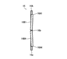
- FIG. 1 is a diagram showing a schematic configuration of a first embodiment of an imaging device according to the present invention.
- the image pickup device of the present embodiment is an image pickup device that captures a 4-band multispectral image.
- the image pickup apparatus of the present embodiment mainly includes an image pickup optical system 10, an image pickup element 100, and a signal processing unit 200.
- the imaging optical system 10 is configured by combining a plurality of lenses 12.
- the imaging optical system 10 has a bandpass filter unit 16 and a polarizing filter unit 18 in its optical path. Further, the imaging optical system 10 has a focus adjusting mechanism (not shown). The focus adjustment mechanism adjusts the focus by, for example, moving the entire imaging optical system 10 back and forth along the optical axis L.
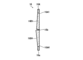
- FIG. 2 is a front view of the bandpass filter unit.
- the bandpass filter unit 16 is composed of a frame body 16A having four opening areas 16A1 to 16A4, and four bandpass filters 16B1 to 16B4 provided in each opening area 16A1 to 16A4 of the frame body 16A.
- the opening area 16A1 is the first opening area 16A1
- the opening area 16A2 is the second opening area 16A2
- the opening area 16A3 is the third opening area 16A3
- the opening area 16A4 is the fourth opening area 16A4.
- Each opening region 16A1 to 16A4 is distinguished by the name.
- the bandpass filter 16B1 provided in the first opening region 16A1 is provided in the first bandpass filter 16B1
- the bandpass filter 16B2 provided in the second opening region 16A2 is provided in the second bandpass filter 16B2 and the third opening region 16A3.
- the bandpass filter 16B3 is referred to as a third bandpass filter 16B3
- the bandpass filter 16B4 provided in the fourth opening region 16A4 is referred to as a fourth bandpass filter 16B4, and the bandpass filters 16B1 to 16B4 are distinguished.
- the frame body 16A has an annular frame body 16a and a partition 16b that partitions the inside of the frame body 16a.
- the frame body 16A is divided into four equal parts in the circumferential direction by a cross-shaped partition 16b inside the frame body 16a, and four opening regions 16A1 to 16A4 are provided.
- the frame body 16a constitutes the diaphragm (aperture diaphragm) of the imaging optical system 10.
- the pupil region is divided into four regions Z1 to Z4 by the frame body 16A (pupil division).
- each of the divided regions Z1 to Z4 will be referred to as a first pupil region Z1, a second pupil region Z2, a third pupil region Z3, and a fourth pupil region Z4, respectively, as necessary.
- the aperture regions 16A1 to 16A4 correspond to the four pupil regions Z1 to Z4 of the imaging optical system 10. That is, the first aperture region 16A1 corresponds to the first pupil region Z1.
- the second aperture region 16A2 corresponds to the second pupil region Z2.
- the third aperture region 16A3 corresponds to the third pupil region Z3.
- the fourth aperture region 16A4 corresponds to the fourth pupil region Z4.
- the wavelength band of light passing through is limited by the bandpass filters 16B1 to 16B4 provided in each aperture region 16A1 to 16A4. That is, in the first pupil region Z1, the wavelength band of the passing light is limited by the first bandpass filter 16B1. In the second pupil region Z2, the wavelength band of light passing through is limited by the second bandpass filter 16B2. In the third pupil region Z3, the wavelength band of light passing through is limited by the third bandpass filter 16B3. In the fourth pupil region Z4, the wavelength band of light passing through is limited by the fourth bandpass filter 16B4.
- the bandpass filters 16B1 to 16B4 are examples of optical elements.
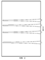
- FIG. 3 is a graph showing an example of the transmission wavelength characteristics of each bandpass filter.
- Each bandpass filter 16B1 to 16B4 transmits light in a different wavelength band. Specifically, the first bandpass filter 16B1 transmits light in the wavelength band ⁇ 1. The second bandpass filter 16B2 transmits light in the wavelength band ⁇ 2. The third bandpass filter 16B3 transmits light in the wavelength band ⁇ 3. The fourth bandpass filter 16B4 transmits light in the wavelength band ⁇ 4.
- each bandpass filter 16B1 to 16B4 has a function of individually correcting the aberration of the region corresponding to each pupil region Z1 to Z4. This point will be described in detail later.
- the imaging optical system 10 has different wavelengths of light passing through the regions corresponding to the pupil regions Z1 to Z4.
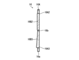
- FIG. 4 is a front view of the polarizing filter unit.
- the polarizing filter unit 18 is composed of a frame body 18A having four opening regions 18A1 and 18A2, and four polarizing filters 18B1 to 18B4 provided in each opening regions 18A1 to 18A4 of the frame body 18A.
- the opening area 18A1 is the first opening area 18A1
- the opening area 18A2 is the second opening area 18A2
- the opening area 18A3 is the third opening area 18A3
- the opening area 18A4 is the fourth opening area 18A4.
- the polarizing filter 18B1 provided in the first opening region 18A1 is used as the first polarizing filter 18B1
- the polarizing filter 18B2 provided in the second opening region 18A2 is used as the second polarizing filter 18B2
- the polarizing filter 18B3 provided in the third opening region 18A3 is used.
- the polarizing filters 18B4 provided in the third polarizing filter 18B3 and the fourth aperture region 18A4 are referred to as the fourth polarizing filter 18B4, and the polarizing filters 18B1 to 18B4 are distinguished from each other.
- the frame body 18A has the same shape as the frame body 16A of the bandpass filter unit 16. Therefore, it has an annular frame body 18a and a partition 18b.
- the frame body 18A is provided with four opening regions 18A1 to 18A4 by dividing the inner peripheral portion of the frame body 18a into four equal parts in the circumferential direction by a cross-shaped partition 18b.
- the opening regions 18A1 to 18A4 are arranged so as to overlap the opening regions 16A1 to 16A4 of the bandpass filter unit 16. That is, the first opening region 18A1 is arranged so as to overlap the first opening region 16A1 of the bandpass filter unit 16.
- the second opening region 18A2 is arranged so as to overlap the second opening region 16A2 of the bandpass filter unit 16.
- the third opening region 18A3 is arranged so as to overlap the third opening region 16A3 of the bandpass filter unit 16.
- the fourth opening region 18A4 is arranged so as to overlap the fourth opening region 16A4 of the bandpass filter unit 16. Therefore, the light that has passed through the first aperture region 16A1 of the bandpass filter unit 16 passes through the first aperture region 18A1 of the polarizing filter unit 18. Further, the light that has passed through the second aperture region 16A2 of the bandpass filter unit 16 passes through the second aperture region 18A2 of the polarizing filter unit 18. Further, the light that has passed through the third aperture region 16A3 of the bandpass filter unit 16 passes through the third aperture region 18A3 of the polarizing filter unit 18. Further, the light that has passed through the fourth aperture region 16A4 of the bandpass filter unit 16 passes through the fourth aperture region 18A4 of the polarizing filter unit 18.
- the polarizing filters 18B1 to 18B4 are examples of polarizers.
- light having different characteristics is emitted from the regions corresponding to the pupil regions Z1 to Z4. That is, light having a polarization direction ⁇ 1 and a wavelength band ⁇ 1 (first light), light having a polarization direction ⁇ 2 and a wavelength band ⁇ 2 (second light), light having a polarization direction ⁇ 3 and a wavelength band ⁇ 3 (third light), Then, (fourth light) having a polarization direction ⁇ 4 and a wavelength band ⁇ 4 is emitted.
- the first light is light that passes through the pupil region Z1 and is light that passes through the first bandpass filter 16B1 and the first polarizing filter 18B1.
- the second light is light that passes through the pupil region Z2, and is light that passes through the second bandpass filter 16B2 and the second polarizing filter 18B2.
- the third light is light that passes through the pupil region Z3, and is light that passes through the third bandpass filter 16B3 and the third polarizing filter 18B3.
- the fourth light is light that passes through the pupil region Z4, and is light that passes through the fourth bandpass filter 16B4 and the fourth polarizing filter 18B4.
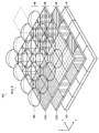
- FIG. 5 is a diagram showing a schematic configuration of an array of pixels of the image sensor.
- the image sensor 100 has a plurality of types of pixels P1 to P16 on its light receiving surface.
- the pixels P1 to P16 are regularly arranged at a constant pitch along the horizontal direction (x-axis direction) and the vertical direction (y-axis direction).
- one pixel block PB (X, Y) is composed of 16 adjacent (4 ⁇ 4) pixels P1 to P16, and the pixel block PB (X, Y) is formed.
- the pixel P1 is the first pixel P1
- the pixel P2 is the second pixel P2
- the pixel P3 is the third pixel P3
- the pixel P4 is the fourth pixel P4
- the pixel P5 is the fifth pixel P5, and the pixel P6.
- the sixth pixel P6, the pixel P7 is the seventh pixel P7, the pixel P8 is the eighth pixel P8, the pixel P9 is the ninth pixel P9, the pixel P10 is the tenth pixel P10, the pixel P11 is the eleventh pixel P11, and the pixel P12 is the twelfth.
- Pixels P12 and P13 are the 13th pixel P13, the pixel P14 is the 14th pixel P14, the pixel P15 is the 15th pixel P15, and the pixel P16 is the 16th pixel P16, and each pixel P1 to P16 is distinguished. Each pixel P1 to P16 has different optical characteristics.
- FIG. 6 is a diagram showing a schematic configuration of an image sensor. Further, FIG. 7 is a cross-sectional view showing a schematic configuration of one pixel (broken line portion in FIG. 6).
- the image pickup device 100 includes a pixel array layer 110, a polarizing filter element array layer 120, a spectroscopic filter element array layer 130, and a microlens array layer 140. Each layer is arranged in the order of the pixel array layer 110, the polarizing filter element array layer 120, the spectroscopic filter element array layer 130, and the microlens array layer 140 from the image plane side to the object side.
- the pixel array layer 110 is configured by arranging a large number of photodiodes 112 two-dimensionally.
- One photodiode 112 constitutes one pixel.
- Each photodiode 112 is regularly arranged along the horizontal direction (x direction) and the vertical direction (y direction).
- the polarizing filter element array layer 120 is configured by two-dimensionally arranging four types of polarizing filter elements 122A to 122D having different polarization directions of the transmitted light.
- the polarizing filter element 122A is the first polarizing filter element 122A
- the polarizing filter element 122B is the second polarizing filter element 122B
- the polarizing filter element 122C is the third polarizing filter element 122C
- the polarizing filter element 122D is the fourth.
- each polarizing filter element 122A to 122D is distinguished.
- the polarizing filter elements 122A to 122D are arranged at the same intervals as the photodiode 112, and are provided for each pixel. In each pixel block PB (X, Y), each polarizing filter element 122A to 122D is regularly arranged.
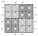
- FIG. 8 is a diagram showing an example of an arrangement pattern of polarizing filter elements in one pixel block.
- the first polarizing filter element 122A is provided in the first pixel P1, the third pixel P3, the ninth pixel P9, and the eleventh pixel P11.
- a second polarizing filter element 122B is provided in the second pixel P2, the fourth pixel P4, the tenth pixel P10, and the twelfth pixel P12.
- the third pixel P3, the seventh pixel P7, the thirteenth pixel P13, and the fifteenth pixel P15 are provided with the third polarizing filter element 122C.
- the 4th pixel P4, the 8th pixel P8, the 14th pixel P14, and the 16th pixel P16 are provided with the fourth polarizing filter element 122D.
- the spectroscopic filter element array layer 130 is configured by two-dimensionally arranging four types of spectroscopic filter elements 132A to 132D having different transmission wavelength characteristics.
- the spectroscopic filter element 132A is the first spectroscopic filter element 132A
- the spectroscopic filter element 132B is the second spectroscopic filter element 132B
- the spectroscopic filter element 132C is the third spectroscopic filter element 132C
- the spectroscopic filter element 132D is the fourth.
- each spectroscopic filter element 132A to 132D is distinguished.
- the spectroscopic filter elements 132A to 132D are arranged at the same intervals as the photodiode 112, and are provided for each pixel. In each pixel block PB (X, Y), the spectroscopic filter elements 132A to 132D are regularly arranged.
- FIG. 9 is a diagram showing an example of an arrangement pattern of spectral filter elements in one pixel block.
- the first spectral filter element 132A is provided in the first pixel P1, the second pixel P2, the fifth pixel P5, and the sixth pixel P6.
- the second spectral filter element 132B is provided in the third pixel P3, the fourth pixel P4, the seventh pixel P7, and the eighth pixel P8.
- the ninth pixel P9, the tenth pixel P10, the thirteenth pixel P13, and the fourteenth pixel P14 are provided with the third spectral filter element 132C.
- the 11th pixel P11, the 12th pixel P12, the 15th pixel P15, and the 16th pixel P16 are provided with the fourth spectral filter element 132D.
- FIG. 10 is a graph showing an example of transmission wavelength characteristics of each spectroscopic filter element.
- A indicates the transmission wavelength characteristic of the first spectral filter element 132A.
- B shows the transmission wavelength characteristic of the second spectral filter element 132B.
- C indicates the transmission wavelength characteristic of the third spectral filter element 132C.
- D indicates the transmission wavelength characteristic of the fourth spectral filter element 132D.
- the spectroscopic filter elements 132A to 132D have different transmission wavelength characteristics.
- the first spectroscopic filter element 132A is composed of a spectroscopic filter element that transmits blue (Blue, B) light
- the second spectroscopic filter element 132B transmits green (Green, G) light
- the third spectroscopic filter element 132C is composed of a spectroscopic filter element that transmits red (Red, R) light
- the fourth spectroscopic filter element 132D is composed of infrared light (Infrared, IR).
- An example is shown in the case of being composed of a spectroscopic filter element for transmitting infrared rays.
- the wavelength bands ⁇ 1 to ⁇ 4 of the light transmitted by the bandpass filters 16B1 to 16B4 of the imaging optical system 10 are within the wavelength band transmitted by the spectral filter elements 132A to 132D.
- the wavelength bands ⁇ 1 to ⁇ 4 of the light transmitted by the bandpass filters 16B1 to 16B4 are set in the region where the wavelength bands transmitted by the spectral filter elements 132A to 132D overlap.
- the transmission wavelength bands of the spectroscopic filter elements 132A to 132D are set so as to cover the transmission wavelength bands of the bandpass filters 16B1 to 16B4 of the imaging optical system 10. Therefore, each spectroscopic filter element 132A to 132D uses a filter that transmits light in a wide band.
- the microlens array layer 140 is configured by arranging a large number of microlenses 142 two-dimensionally. Each microlens 142 is arranged at the same spacing as the photodiode 112 and is provided for each pixel. The microlens 142 is provided for the purpose of efficiently condensing the light from the imaging optical system 10 on the photodiode 112.
- each pixel P1 to P16 receives light from the image pickup optical system 10 as follows. That is, the first pixel P1 receives light from the imaging optical system 10 via the first spectral filter element 132A (transmission wavelength characteristic A) and the first polarizing filter element 122A (polarization direction ⁇ A). Further, the second pixel P2 receives light from the imaging optical system 10 via the first spectral filter element 132A (transmission wavelength characteristic A) and the second polarizing filter element 122B (polarization direction ⁇ B).
- the third pixel P3 receives light from the imaging optical system 10 via the second spectral filter element 132B (transmission wavelength characteristic B) and the first polarizing filter element 122A (polarization direction ⁇ A). Further, the fourth pixel P4 receives light from the imaging optical system 10 via the second spectral filter element 132B (transmission wavelength characteristic B) and the second polarizing filter element 122B (polarization direction ⁇ B). Further, the fifth pixel P5 receives light from the imaging optical system 10 via the first spectral filter element 132A (transmission wavelength characteristic A) and the third polarizing filter element 122C (polarization direction ⁇ C).
- the sixth pixel P6 receives light from the imaging optical system 10 via the first spectral filter element 132A (transmission wavelength characteristic A) and the fourth polarizing filter element 122D (polarization direction ⁇ D). Further, the seventh pixel P7 receives light from the imaging optical system 10 via the second spectral filter element 132B (transmission wavelength characteristic B) and the third polarizing filter element 122C (polarization direction ⁇ C). Further, the eighth pixel P8 receives light from the imaging optical system 10 via the second spectral filter element 132B (transmission wavelength characteristic B) and the fourth polarizing filter element 122D (polarization direction ⁇ D).
- the ninth pixel P9 receives light from the imaging optical system 10 via the third spectral filter element 132C (transmission wavelength characteristic C) and the first polarizing filter element 122A (polarization direction ⁇ A). Further, the tenth pixel P10 receives light from the imaging optical system 10 via the third spectral filter element 132C (transmission wavelength characteristic C) and the second polarizing filter element 122B (polarization direction ⁇ B). Further, the 11th pixel P11 receives light from the imaging optical system 10 via the fourth spectral filter element 132D (transmission wavelength characteristic D) and the first polarizing filter element 122A (polarization direction ⁇ A).
- the 12th pixel P12 receives light from the imaging optical system 10 via the fourth spectral filter element 132D (transmission wavelength characteristic D) and the second polarization filter element 122B (polarization direction ⁇ B). Further, the 13th pixel P13 receives light from the imaging optical system 10 via the third spectral filter element 132C (transmission wavelength characteristic C) and the third polarizing filter element 122C (polarization direction ⁇ C). Further, the 14th pixel P14 receives light from the imaging optical system 10 via the third spectral filter element 132C (transmission wavelength characteristic C) and the fourth polarizing filter element 122D (polarization direction ⁇ D).
- the 15th pixel P15 receives light from the imaging optical system 10 via the fourth spectral filter element 132D (transmission wavelength characteristic D) and the third polarizing filter element 122C (polarization direction ⁇ C). Further, the 16th pixel P16 receives light from the imaging optical system 10 via the fourth spectral filter element 132D (transmission wavelength characteristic D) and the fourth polarizing filter element 122D (polarization direction ⁇ D). As described above, each of the pixels P1 to P16 receives light having different characteristics by having different optical characteristics from each other. That is, it receives light having different wavelength bands and polarization directions.
- the signal processing unit 200 processes the signal output from the image sensor 100 to generate image data of a 4-band multispectral image. That is, image data of four types of wavelength bands ⁇ 1 to ⁇ 4 that pass through the bandpass filter unit 16 of the imaging optical system 10 are generated.
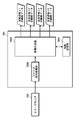
- FIG. 11 is a block diagram showing a schematic configuration of a signal processing unit.
- the signal processing unit 200 includes an analog signal processing unit 200A, an image generation unit 200B, and a coefficient storage unit 200C.
- the analog signal processing unit 200A takes in the analog pixel signal output from each pixel of the image pickup element 100, performs predetermined signal processing (for example, correlation double sampling processing, amplification processing, etc.), and then converts it into a digital signal. And output.
- predetermined signal processing for example, correlation double sampling processing, amplification processing, etc.
- the image generation unit 200B performs predetermined signal processing on the pixel signal after being converted into a digital signal, and generates image data in each wavelength band ⁇ 1 to ⁇ 4.
- FIG. 12 is a conceptual diagram of image generation.
- Each pixel block PB (X, Y) includes 16 pixels P1 to P16. Therefore, 16 image data D1 to D16 are generated by separating and extracting the pixel signals of the pixels P1 to P16 from the pixel blocks PB (X, Y). However, interference (crosstalk) has occurred in the 16 image data D1 to D16. That is, since light in each wavelength band is incident on each pixel P1 to P16, the generated image is an image in which images in each wavelength band are mixed at a predetermined ratio. Therefore, the image generation unit 200B performs the interference removal process to generate image data in each wavelength band.
- the pixel signal (signal value) obtained from the first pixel P1 of each pixel block PB (X, Y) is ⁇ 1
- the pixel signal obtained from the second pixel P2 is ⁇ 2
- the pixel signal obtained from the third pixel P3 is ⁇ 3.
- the pixel signal obtained by the 4th pixel P4 is ⁇ 4, the pixel signal (signal value) obtained by the 5th pixel P5 is ⁇ 5, the pixel signal obtained by the 6th pixel P6 is ⁇ 6, and the pixel signal obtained by the 7th pixel P7 is ⁇ 7, the pixel signal obtained by the eighth pixel P8 is ⁇ 8, the pixel signal (signal value) obtained by the ninth pixel P9 is ⁇ 9, the pixel signal (signal value) obtained by the first pixel P1 is ⁇ 1, and the second pixel P2.
- the pixel signal obtained in the above is ⁇ 2, the pixel signal obtained in the third pixel P3 is ⁇ 3, the pixel signal obtained in the fourth pixel P4 is ⁇ 4, and the pixel signal (signal value) obtained in the tenth element P10 is ⁇ 10, eleventh.
- the pixel signal (signal value) obtained by the pixel P11 is ⁇ 11
- the pixel signal obtained by the 12th pixel P12 is ⁇ 12
- the pixel signal obtained by the 13th pixel P13 is ⁇ 13
- the pixel signal obtained by the 14th pixel P14 is ⁇ 14.
- the pixel signal (signal value) obtained by the 15th pixel P15 is ⁇ 15
- the pixel signal obtained by the 16th pixel P16 is ⁇ 16.
- 16 pixel signals ⁇ 1 to ⁇ 16 can be obtained.
- the image generation unit 200B calculates four pixel signals ⁇ 1 to ⁇ 4 corresponding to light in each wavelength band ⁇ 1 to ⁇ 4 from the 16 pixel signals ⁇ 1 to ⁇ 16, and removes interference. Specifically, four pixel signals ⁇ 1 to ⁇ 4 corresponding to light in each wavelength band ⁇ 1 to ⁇ 4 are calculated by Equation 1 using the following matrix A, and interference is eliminated.
- the pixel signal ⁇ 1 is a pixel signal corresponding to light in the wavelength band ⁇ 1
- the pixel signal ⁇ 2 is a pixel signal corresponding to light in the wavelength band ⁇ 2
- the pixel signal ⁇ 3 is a pixel signal corresponding to light in the wavelength band ⁇ 3, and the pixel signal ⁇ 4.
- the reason why the interference can be eliminated by the above equation 1 will be described.
- Interference occurs when light in each wavelength band ⁇ 1 to ⁇ 4 is mixed into each pixel P1 to P16.
- b11 is the ratio of light in the wavelength band ⁇ 1 received by the first pixel P1
- b12 is the ratio of light in the wavelength band ⁇ 2 received by the first pixel P1
- b13 is the ratio of light in the wavelength band ⁇ 3.
- the ratio of light received by the first pixel P1, b14 is the ratio of light in the wavelength band ⁇ 4 received by the first pixel P1.
- b21 is the ratio of light in the wavelength band ⁇ 1 received by the second pixel P2
- b22 is the ratio of light received in the wavelength band ⁇ 2 by the second pixel P2
- b23 is the ratio of light in the wavelength band ⁇ 3.
- the ratio of light received by the two pixels P2, b24 is the ratio of light received in the wavelength band ⁇ 4 received by the second pixel P2.
- b31 is the ratio of light in the wavelength band ⁇ 1 received by the third pixel P3
- b32 is the ratio of light received in the wavelength band ⁇ 2 by the third pixel P3,
- b33 is the ratio of light in the wavelength band ⁇ 3.
- the ratio of light received by the three pixels P3, b34 is the ratio of light received in the wavelength band ⁇ 4 received by the third pixel P3. Further, b41 is the ratio of light in the wavelength band ⁇ 1 received by the fourth pixel P4, b42 is the ratio of light received in the wavelength band ⁇ 2 by the fourth pixel P4, and b43 is the ratio of light in the wavelength band ⁇ 3. The ratio of light received by the four pixels P4, b44, is the ratio of light received in the wavelength band ⁇ 4 received by the fourth pixel P4.
- b51 is the ratio of light in the wavelength band ⁇ 1 received by the fifth pixel P5
- b52 is the ratio of light received in the wavelength band ⁇ 2 by the fifth pixel P5
- b53 is the ratio of light in the wavelength band ⁇ 3.
- the ratio of light received by the 5th pixel P5, b54 is the ratio of light received in the wavelength band ⁇ 4 being received by the 5th pixel P5.
- b61 is the ratio of light in the wavelength band ⁇ 1 received by the sixth pixel P6, b62 is the ratio of light in the wavelength band ⁇ 2 received by the sixth pixel P6, and b63 is the ratio of light in the wavelength band ⁇ 3.
- the ratio of light received by the 6-pixel P6, b64 is the ratio of the light in the wavelength band ⁇ 4 received by the 6-pixel P6.
- b71 is the ratio of light in the wavelength band ⁇ 1 received by the seventh pixel P7
- b72 is the ratio of light in the wavelength band ⁇ 2 received by the seventh pixel P7
- b73 is the ratio of light in the wavelength band ⁇ 3.
- the ratio of light received by the 7-pixel P7, b74 is the ratio of the light in the wavelength band ⁇ 4 received by the 7th pixel P7.
- b81 is the ratio of light in the wavelength band ⁇ 1 received by the eighth pixel P8
- b82 is the ratio of light received in the wavelength band ⁇ 2 by the eighth pixel P8
- b83 is the ratio of light in the wavelength band ⁇ 3.
- the ratio of light received by the eight pixels P8, b84 is the ratio of light received in the wavelength band ⁇ 4 being received by the eighth pixel P8.
- b91 is the ratio of light in the wavelength band ⁇ 1 received by the ninth pixel P9
- b92 is the ratio of light received in the wavelength band ⁇ 2 in the ninth pixel P9
- b93 is the ratio of light in the wavelength band ⁇ 3.
- the ratio of light received by the 9-pixel P9, b94 is the ratio of the light in the wavelength band ⁇ 4 received by the 9th pixel P9.
- b101 is the ratio of light in the wavelength band ⁇ 1 received by the 10th pixel P10
- b102 is the ratio of light received in the wavelength band ⁇ 2 in the 10th pixel P10
- b103 is the ratio of light in the wavelength band ⁇ 3.
- the ratio of light received by the 10 pixels P10, b104 is the ratio of light received in the wavelength band ⁇ 4 received by the 10th pixel P10.
- b111 is the ratio of light in the wavelength band ⁇ 1 received by the 11th pixel P11
- b112 is the ratio of light in the wavelength band ⁇ 2 received by the 11th pixel P11
- b113 is the ratio of light in the wavelength band ⁇ 3.
- the ratio of light received by the 11th pixel P11, b114, is the ratio of light received in the wavelength band ⁇ 4 being received by the 11th pixel P11.
- b121 is the ratio of light in the wavelength band ⁇ 1 received by the 12th pixel P12
- b122 is the ratio of light received in the wavelength band ⁇ 2 in the 12th pixel P12
- b123 is the ratio of light in the wavelength band ⁇ 3.
- the ratio of light received by the 12-pixel P12, b124 is the ratio of the light in the wavelength band ⁇ 4 received by the 12-pixel P12. Further, b131 is the ratio of light in the wavelength band ⁇ 1 received by the 13th pixel P13, b132 is the ratio of light received in the wavelength band ⁇ 2 by the 13th pixel P13, and b133 is the ratio of light in the wavelength band ⁇ 3.
- the ratio of light received by the 13-pixel P13, b134 is the ratio of the light in the wavelength band ⁇ 4 received by the 13-pixel P13.
- b141 is the ratio of light in the wavelength band ⁇ 1 received by the 14th pixel P14
- b142 is the ratio of light received in the wavelength band ⁇ 2 in the 14th pixel P14
- b143 is the ratio of light in the wavelength band ⁇ 3.
- the ratio of light received by the 14-pixel P14, b144, is the ratio of light in the wavelength band ⁇ 4 received by the 14-pixel P14.
- b151 is the ratio of light in the wavelength band ⁇ 1 received in the 15th pixel P15
- b152 is the ratio of light in the wavelength band ⁇ 2 received in the 15th pixel P15
- b153 is the ratio of light in the wavelength band ⁇ 3.
- the ratio of light received by the 15 pixels P15, b154, is the ratio of light received in the wavelength band ⁇ 4 received by the 15th pixel P15.
- b161 is the ratio of light in the wavelength band ⁇ 1 received by the 16th pixel P16
- b162 is the ratio of light received in the wavelength band ⁇ 2 in the 16th pixel P16
- b163 is the ratio of light in the wavelength band ⁇ 3.
- the ratio of light received by the 16-pixel P16, b164, is the ratio of light in the wavelength band ⁇ 4 received by the 16th pixel P16.
- This ratio bij sets the wavelength bands ⁇ 1 to ⁇ 4 of the light transmitted by the opening regions 16A1 to 16A4 of the bandpass filter unit 16, and the polarization direction ⁇ 1 of the light transmitted by the opening regions 18A1 to 18A4 of the polarizing filter unit 18. It is uniquely determined from the setting of ⁇ 2, the transmission wavelength characteristics A to D of the pixels P1 to P16 of the image pickup element 100, and the polarization directions ⁇ A to ⁇ C of the light received by the pixels P1 to P16 of the image pickup element 100. Can be asked for.
- the following relationship is between the pixel signals ⁇ 1 to ⁇ 16 obtained from the pixels P1 to P16 of each pixel block PB (X, Y) and the pixel signals ⁇ 1 to ⁇ 4 corresponding to the light of each wavelength band ⁇ 1 to ⁇ 4. Holds.
- ⁇ 1 to ⁇ 4 which are the solutions of the simultaneous equations of equations 2 to 17, are calculated by multiplying both sides of the above equation 18 by the inverse matrix B -1 of the matrix B.
- the light of the respective wavelength bands ⁇ 1 to ⁇ 4 emitted from the imaging optical system 10 is the light of each pixel P1 of the pixel block PB (X, Y). It can be calculated from the signal values (pixel signals) ⁇ 1 to ⁇ 16 of each pixel P1 to P16 based on the ratio of light received by ⁇ P16.
- the coefficient storage unit 200C stores each element aij of the matrix A for performing the interference removal process as a coefficient group.
- the image generation unit 200B acquires a coefficient group from the coefficient storage unit 200C, and from the pixel signals ⁇ 1 to ⁇ 16 obtained from the pixels P1 to P16 of each pixel block PB (X, Y), each wavelength band is obtained by the above equation 1. Pixel signals ⁇ 1 to ⁇ 4 corresponding to ⁇ 1 to ⁇ 4 are calculated, and image data of each wavelength band ⁇ 1 to ⁇ 4 is generated.
- the image data of each wavelength band ⁇ 1 to ⁇ 4 generated by the image generation unit 200B is output to the outside and stored in a storage device (not shown) as needed. In addition, it is displayed on a display (not shown) as needed.
- FIG. 13 is a conceptual diagram of image generation by the imaging device.
- the light incident on the image pickup optical system 10 becomes four types of light having different characteristics and is incident on the image pickup element 100. Specifically, light having a polarization direction ⁇ 1 and a wavelength band ⁇ 1 (first light), light having a polarization direction ⁇ 1 and a wavelength band ⁇ 2 (second light), and light having a polarization direction ⁇ 2 and a wavelength band ⁇ 3 (third light). Light) and (fourth light) having a polarization direction ⁇ 2 and a wavelength band ⁇ 4 are incident on the image pickup element 100.
- each pixel block PB (X, Y) of the image sensor 100 light in each wavelength band emitted from the image pickup optical system 10 is received in each pixel P1 to P16 at a predetermined ratio bij. That is, due to the action of the polarizing filter elements 122A to 122D and the spectroscopic filter elements 132A to 132D provided in the pixels P1 to P16, the light in each wavelength band ⁇ 1 to ⁇ 4 is received at a predetermined ratio bij.
- the signal processing unit 200 has pixel signals ⁇ 1 to ⁇ 4 corresponding to light in each wavelength band ⁇ 1 to ⁇ 4 from pixel signals ⁇ 1 to ⁇ 16 obtained from pixels P1 to P16 of each pixel block PB (X, Y) of the image sensor 100. Is calculated, and image data of each wavelength band ⁇ 1 to ⁇ 4 is generated. That is, arithmetic processing (interference removal processing) according to Equation 1 using the matrix A is performed to correspond to light in each wavelength band ⁇ 1 to ⁇ 4 from the pixel signals ⁇ 1 to ⁇ 16 of the pixels P1 to P16 obtained from the image sensor 100. The pixel signals ⁇ 1 to ⁇ 4 are calculated, and image data of each wavelength band ⁇ 1 to ⁇ 4 is generated.
- one image pickup optical system 10 and one (single plate) image pickup element 100 capture images of four different wavelength bands (four-band multispectral images). it can.
- the imaging apparatus 1 of the present embodiment captures a multispectral image by dividing the pupil region of the imaging optical system 10 into a plurality of regions (pupil division) and limiting the wavelength region in each region. Is possible.
- the "general imaging optical system” here means an imaging optical system in which aberrations for each wavelength are not particularly corrected, that is, an imaging optical system in which aberrations for each wavelength remain.
- the bandpass filters 16B1 to 16B4 have a function of individually correcting the aberrations in the regions corresponding to the pupil regions Z1 to Z4.
- each bandpass filter 16B1 to 16B4 has a lens shape having a curvature on at least one surface on the object side and the image side, and the curvature is individually adjusted to cause aberration in the corresponding region. It is corrected individually. That is, by giving the bandpass filter a lens function, the optical path lengths of the regions corresponding to the pupil regions Z1 to Z4 are individually adjusted to correct the aberration.
- FIG. 14 is a 14-14 cross-sectional view of the bandpass filter unit shown in FIG.
- the figure shows a cross section of the first bandpass filter 16B1 and the fourth bandpass filter 16B4.
- 15 is a 15-15 cross-sectional view of the bandpass filter unit shown in FIG. 2.
- FIG. The figure shows the cross section of the second bandpass filter 16B2 and the third bandpass filter 16B3.
- each of the bandpass filters 16B1 to 16B4 has a curved surface on one side (the surface on the object side (left side in FIGS. 14 and 15)).
- the curvature of one side of the bandpass filters 16B1 to 16B4 is individually adjusted, and the aberration of the region corresponding to each pupil region Z1 to Z4 is corrected.
- the aberration of the region corresponding to the first pupil region Z1 is corrected by adjusting the curvature of one side of the first bandpass filter 16B1.
- the aberration is corrected by adjusting the curvature of one side of the second bandpass filter 16B2.
- the aberration is corrected by adjusting the curvature of one side of the third bandpass filter 16B3. Further, for the region corresponding to the fourth pupil region Z4, the aberration is corrected by adjusting the curvature of the surface of the fourth bandpass filter 16B4 on the object side.
- each bandpass filter 16B1 to 16B4 changes by changing the curvature of one side. Let the focal lengths at the center wavelength of the light passing through the pupil regions Z1 to Z4 of the imaging optical system 10 be f1, f2, f3, and f4. The focal lengths of the bandpass filters 16B1 to 16B4 are shortened in descending order of the focal lengths f1, f2, f3, and f4.
- the imaging optical system 10 the aberrations in the regions corresponding to the pupil regions Z1 to Z4 are individually corrected by the bandpass filters 16B1 to 16B4. As a result, the imaging optical system 10 has different aberration characteristics in the regions corresponding to the pupil regions Z1 to Z4.
- the aberrations in the regions corresponding to the pupil regions Z1 to Z4 can be individually controlled, so that the aberrations can be controlled for each wavelength. This makes it possible to capture a multispectral image with good image quality.
- the method of this embodiment can also be applied to an existing imaging lens (general imaging lens not for multispectral imaging). That is, since the method of the present embodiment only arranges a bandpass filter in each pupil-divided region and adjusts the curvature of each bandpass filter, it can be applied to an existing imaging lens. Therefore, by using the method of the present embodiment, the existing imaging lens can be used as an imaging lens for multispectral imaging.
- an existing imaging lens generally imaging lens not for multispectral imaging. That is, since the method of the present embodiment only arranges a bandpass filter in each pupil-divided region and adjusts the curvature of each bandpass filter, it can be applied to an existing imaging lens. Therefore, by using the method of the present embodiment, the existing imaging lens can be used as an imaging lens for multispectral imaging.
- each bandpass filter 16B1 to 16B4 has a curvature on only one side, but both sides may have a curvature.
- the imaging optical system has a configuration in which the wavelengths of light passing through each pupil region are different from each other and the aberration characteristics of the regions corresponding to each pupil region are different from each other.
- the bandpass filters 16B1 to 16B4 provided in the regions corresponding to the pupil regions Z1 to Z4 limit the wavelength band of light passing through the regions corresponding to the pupil regions Z1 to Z4.
- the bandpass filters 16B1 to 16B4 provided in the regions corresponding to the pupil regions Z1 to Z4 individually correct the aberrations in the regions corresponding to the pupil regions Z1 to Z4, and correspond to the pupil regions Z1 to Z4. It is assumed that the aberration characteristics of the regions to be affected are different from each other. It is the same as the imaging device 1 of the first embodiment, except that the aberration correction method is different. Therefore, here, the aberration correction method by the bandpass filters 16B1 to 16B4 will be described.
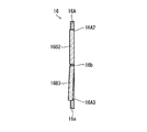
- FIG. 16 is a diagram showing the configuration of the bandpass filter unit of the present embodiment.
- (A) shows a side view of the bandpass filter unit
- (B) shows a front view of the bandpass filter unit.
- FIG. 17 is a cross-sectional view taken along the line 17-17 of FIG.
- the figure shows a cross section of the first bandpass filter 16B1 and the fourth bandpass filter 16B4.
- 18 is a cross-sectional view taken along the line 18-18 of FIG.
- the figure shows the cross section of the second bandpass filter 16B2 and the third bandpass filter 16B3.
- the bandpass filters 16B1 to 16B4 of the present embodiment have a flat plate shape.
- the imaging optical system 10 is formed by individually adjusting the thicknesses t1 to t4 of the bandpass filters 16B1 to B4 (thicknesses in the direction parallel to the optical axis L) to cover the regions corresponding to the pupil regions Z1 to Z4. Aberrations are corrected individually. That is, due to the difference in thickness t1 to t4, even if the object distance is the same for the entire imaging optical system 10, the object distance for the rear group changes, and the position of the final image plane changes for each wavelength band. Can be done.
- the axial chromatic aberration (deviation of the imaging position for each color) of the imaging optical system 10 is corrected individually for each wavelength band by changing the thicknesses t1 to t4 of the bandpass filters 16B1 to 16B4. it can.
- the focal lengths at the center wavelengths of the light passing through the pupil regions Z1 to Z4 of the imaging optical system 10 are f1, f2, f3, and f4
- each band path is in ascending order of focal lengths f1, f2, f3, and f4.
- the thicknesses t1 to t4 of the filters 16B1 to 16B4 are increased.
- the aberration of the region corresponding to each pupil region Z1 to Z4 can be individually controlled, so that the aberration can be controlled for each wavelength. This makes it possible to capture a multispectral image with good image quality. Further, since the method of the present embodiment can also be applied to an existing imaging lens, the existing imaging lens can be used as an imaging lens for multispectral imaging.
- the imaging optical system has a configuration in which the wavelengths of light passing through each pupil region are different from each other and the aberration characteristics of the regions corresponding to each pupil region are different from each other.
- the bandpass filters 16B1 to 16B4 provided in the regions corresponding to the pupil regions Z1 to Z4 limit the wavelength band of light passing through the regions corresponding to the pupil regions Z1 to Z4.
- the bandpass filters 16B1 to 16B4 provided in the regions corresponding to the pupil regions Z1 to Z4 individually correct the aberrations in the regions corresponding to the pupil regions Z1 to Z4, and correspond to the pupil regions Z1 to Z4. It is assumed that the aberration characteristics of the regions to be affected are different from each other. It is the same as the imaging device 1 of the first embodiment, except that the aberration correction method is different. Therefore, here, the aberration correction method by the bandpass filters 16B1 to 16B4 will be described.
- FIG. 19 is a diagram showing the configuration of the bandpass filter unit of the present embodiment.
- (A) shows a side view of the bandpass filter unit
- (B) shows a front view of the bandpass filter unit.
- FIG. 20 is a cross-sectional view taken along the line 20-20 of FIG.
- the figure shows a cross section of the first bandpass filter 16B1 and the fourth bandpass filter 16B4.
- 21 is a cross-sectional view taken along the line 21-21 of FIG.
- the figure shows the cross section of the second bandpass filter 16B2 and the third bandpass filter 16B3.
- the bandpass filters 16B1 to 16B4 of the present embodiment have a flat plate shape.
- the imaging optical system 10 individually adjusts the inclinations of the bandpass filters 16B1 to B4 to individually correct the aberrations in the regions corresponding to the pupil regions Z1 to Z4.
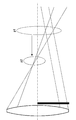
- FIG. 22 is a diagram schematically showing how the imaging position shifts due to asymmetric pupil division in a lens in which coma aberration remains.
- the position p1 indicates the image formation position when the pupil is not divided
- the position p2 indicates the image formation position when the pupil is divided.
- the central imaging position can be shifted by dividing the pupil in a state where coma is generated at the central imaging point.
- axial chromatic aberration can be suppressed for each wavelength band passing through the respective pupil regions Z1 to Z4. That is, since the imaging position can be changed for each wavelength band, the axial chromatic aberration inherent in the imaging optical system 10 can be canceled for each wavelength band.
- FIG. 23 is a conceptual diagram of tilt setting.
- the focal length at the d-line (587.6 nm (yellow) emission line spectrum) of the optical system in front of the aperture is f0, and the focal length at the center wavelength of the wavelength band of light passing through the regions corresponding to the respective pupil regions Z1 to Z4. Let it be f1, f2, f3, and f4, respectively.
- ⁇ be the angle with the rotation center of the vector orthogonal to the vector drawn from the center to the center of gravity of the aperture in the aperture plane. The angle ⁇ is positive in the direction of tilting toward the object.
- the angle ⁇ is increased in ascending order of focal lengths f1, f2, f3, and f4.
- the focal length f0 on the d-line of the optical system on the front side of the diaphragm is f ⁇ 0
- the angle ⁇ is increased in descending order of the focal lengths f1, f2, f3, and f4.
- FIG. 24 is a diagram showing another example of the bandpass filter unit of the present embodiment.
- (A) shows a side view of the bandpass filter unit
- (B) shows a front view of the bandpass filter unit.
- FIG. 25 is a cross-sectional view taken along the line 25-25 of FIG. 24.
- the figure shows a cross section of the first bandpass filter 16B1 and the fourth bandpass filter 16B4.
- 26 is a cross-sectional view taken along the line 26-26 of FIG. 24.
- the figure shows the cross section of the second bandpass filter 16B2 and the third bandpass filter 16B3.
- the bandpass filters 16B1 to 16B4 of this example have a flat plate shape with an inclination on one side (the cross section has a wedge shape).
- the imaging optical system 10 individually corrects the aberration in the region corresponding to each pupil region Z1 to Z4.
- the pupil region of the imaging optical system is equally divided in the circumferential direction, but the mode of division of the pupil region is not limited to this.
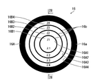
- FIG. 27 is a diagram showing another example (modification example) of the division mode of the pupil region. This figure corresponds to the front view of the bandpass filter unit.
- the pupil region is divided into a plurality of regions by dividing the inner peripheral portion of the frame body 16a constituting the diaphragm into a plurality of regions.
- the inner peripheral portion of the frame body 16a is divided concentrically by a plurality of ring-shaped partitions 16b, and the pupil region of the imaging optical system is divided into a plurality of regions. ..
- FIG. 27 shows an example of the case where the pupil region is divided into four regions.
- the four aperture regions of the frame 16A (first aperture region 16A1, second aperture region 16A2, third aperture region 16A3, fourth aperture region 16A4) each have four pupil regions (first pupil region Z1, second pupil). It corresponds to the area Z2, the third pupil area Z3, and the fourth pupil area Z4). That is, the first aperture region 16A1 corresponds to the first pupil region Z1.
- the second aperture region 16A2 corresponds to the second pupil region Z2.
- the third aperture region 16A3 corresponds to the third pupil region Z3.
- the fourth aperture region 16A4 corresponds to the fourth pupil region Z4.
- the points that the wavelengths of the light passing through the pupil regions Z1 to Z4 are different from each other and the aberration characteristics of the regions corresponding to the pupil regions Z1 to Z4 are different from each other are the same as those of the imaging optical system of the above embodiment. is there. That is, in the imaging optical system, the wavelength band of light passing through the regions corresponding to the pupil regions Z1 to Z4 is limited by the bandpass filters 16B1 to 16B4 provided in the aperture regions 16A1 to 16A4. Further, the bandpass filters 16B1 to 16B4 individually correct the aberrations in the regions corresponding to the pupil regions Z1 to Z4.
- FIG. 28 is a diagram showing an example of a case where the curvature of the bandpass filter is adjusted to correct the aberration. This figure corresponds to the 28-28 cross-sectional view of FIG. 27.
- This example shows an example in which the shape of each bandpass filter 16B1 to 16B4 is set as a lens shape and the aberration of the region corresponding to each pupil region Z1 to Z4 is corrected by individually adjusting the curvature thereof. ..
- only one side (the surface on the object side) of the bandpass filters 16B1 to 16B4 has a curvature, but it is also possible to give a curvature to both sides. Further, the surface on the image side may be configured to have a curvature.
- the wavelength band assigned to each pupil region Z1 to Z4 it is preferable to set the wavelength band assigned to each pupil region Z1 to Z4 according to the required image quality (high image quality is required). Allocate the wavelength band to the central pupil region.
- FIG. 29 is a diagram showing another example of the aberration correction method. The figure shows an example in which the thickness of the bandpass filter is adjusted to correct the aberration.
- each bandpass filter 16B1 to 16B4 is formed into a flat plate shape, and the aberration of the region corresponding to each pupil region Z1 to Z4 is corrected by individually adjusting the thickness thereof.
- FIG. 30 is a diagram showing another example of the aberration correction method. The figure shows an example of a case where the inclination of the bandpass filter is adjusted to correct the aberration.
- each bandpass filter 16B1 to 16B4 is made into a flat plate shape, and the aberration of the region corresponding to each pupil region Z1 to Z4 is corrected by individually adjusting the inclination of one side thereof. ing.
- FIG. 30 shows an example of adjusting the inclination of one side of each bandpass filter
- the inclination of the bandpass filter itself is adjusted to obtain aberrations in the regions corresponding to the pupil regions Z1 to Z4. It can also be configured to be corrected.
- each pupil region Z1 to Z4 it is possible to correct the aberration in the region corresponding to each pupil region Z1 to Z4.
- the curvature of the first bandpass filter is adjusted to correct the aberration
- the thickness of each bandpass filter 16B2 to 16B4 is adjusted. Then, the aberration can be corrected.
- ⁇ Fifth Embodiment When a multispectral image is captured by dividing the pupil region of the imaging optical system, a good dynamic range cannot be obtained if the difference in the amount of light for each wavelength band is large. For example, only an image in a specific wavelength band may be darkened or overexposed.
- the aperture area of each pupil region is adjusted individually, and the amount of light for each wavelength band is adjusted individually.
- the adjustment of the opening area of each pupil region is realized by adjusting the area (opening area) of each opening region of the frame body constituting the bandpass filter unit. It is the same as the imaging device 1 of the first embodiment, except that the aperture area of each pupil region is adjusted by the bandpass filter unit. Therefore, only the configuration of the bandpass filter unit will be described here.
- FIG. 31 is a diagram showing the configuration of the bandpass filter unit of the present embodiment.
- the outer peripheral diameters of the opening regions 16A1 to 16A4 are individually adjusted, and the areas (opening areas) of the opening regions 16A1 to 16A4 are individually adjusted. Is adjusted to.
- the areas of the respective aperture regions 16A1 to 16A4 are individually adjusted, so that the aperture areas of the corresponding pupil regions Z1 to Z4 are individually adjusted.
- the aperture area of each pupil region Z1 to Z4 is individually adjusted, so that the amount of light passing through each pupil region Z1 to Z4 is individually adjusted.
- the amount of light passing through each pupil region Z1 to Z4 is different from each other.
- each pupil region Z1 to Z4 by reducing the opening area of each pupil region Z1 to Z4, it is possible to reduce the aberration of the region corresponding to each pupil region Z1 to Z4. Therefore, by individually adjusting the opening area of each pupil region Z1 to Z4, the aberration of the region corresponding to each pupil region Z1 to Z4 can be individually corrected. For example, the opening area is reduced as the distance from the d line increases. Since a normal image pickup lens is designed with reference to the vicinity of the d line, the aberration increases as the distance from the d line increases. Therefore, it is preferable to reduce the aperture area and reduce the aberration as the wavelength becomes farther from the d line.
- each opening area 16A1 to 16A4 is changed to adjust the area of each opening area 16A1 to 16A4, but the method of adjusting the area of each opening area 16A1 to 16A4. Is not limited to this.
- the area of each opening region 16A1 to 16A4 can be adjusted by changing the width of the partition 16b.
- ⁇ 6th Embodiment As described above, by individually adjusting the amount of light passing through each pupil region Z1 to Z4, the amount of light for each wavelength band can be individually adjusted, and a good dynamic range can be obtained.
- the aperture areas of the pupil regions Z1 to Z4 are individually adjusted, and the amount of light passing through the pupil regions Z1 to Z4 is individually adjusted.
- the transmittance of the bandpass filters 16B1 to 16B4 provided corresponding to the pupil regions Z1 to Z4 is adjusted to adjust the amount of light passing through the pupil regions Z1 to Z4.
- FIG. 32 is a graph showing an example of the transmission wavelength characteristics of each bandpass filter provided in the bandpass filter unit of the present embodiment.
- the first bandpass filter 16B1 transmits light in the wavelength band ⁇ 1.
- the second bandpass filter 16B2 transmits light in the wavelength band ⁇ 2.
- the third bandpass filter 16B3 transmits light in the wavelength band ⁇ 3.
- the fourth bandpass filter 16B4 transmits light in the wavelength band ⁇ 4.
- each bandpass filter 16B1 to 16B4 transmits light in each wavelength band ⁇ 1 to ⁇ 4 with different transmittances.
- the transmittance of the bandpass filters 16B1 to 16B4 provided corresponding to the pupil regions Z1 to Z4 is individually adjusted, and the amount of light passing through the pupil regions Z1 to Z4 is individually adjusted. You can also. As a result, a good dynamic range can be obtained.
- the resolution is also good by controlling the transmittance as in the present embodiment. Image can be obtained.
- the adjustment method of the present embodiment can also be used in combination with the method of adjusting the opening area of each pupil region Z1 to Z4.
- the bandwidth of the light passing through the pupil regions Z1 to Z4 is adjusted to adjust the amount of light passing through the pupil regions Z1 to Z4.
- the bandwidth of the light passing through the pupil regions Z1 to Z4 is adjusted by changing the bandwidth of the wavelength transmitted by the bandpass filters 16B1 to 16B4.
- FIG. 33 is a graph showing an example of the transmission wavelength characteristics of each bandpass filter provided in the bandpass filter unit of the present embodiment.
- the bandpass filters 16B1 to 16B4 have different bandwidths of the wavelength bands ⁇ 1 to ⁇ 4 to be transmitted.
- the amount of light in the first pupil region Z1 is adjusted by adjusting the bandwidth of the wavelength band ⁇ 1 transmitted by the first bandpass filter 16B1.
- the amount of light in the second pupil region Z2 is adjusted by adjusting the bandwidth of the wavelength band ⁇ 2 transmitted by the second bandpass filter 16B2.
- the amount of light in the third pupil region Z3 is adjusted by adjusting the bandwidth of the wavelength band ⁇ 3 transmitted by the third bandpass filter 16B3.
- the amount of light in the fourth pupil region Z4 is adjusted by adjusting the bandwidth of the wavelength band ⁇ 4 transmitted by the fourth bandpass filter 16B4.
- the bandwidth of the wavelength bands ⁇ 1 to ⁇ 4 transmitted by the bandpass filters 16B1 to 16B4 can be individually adjusted, and the amount of light passing through the pupil regions Z1 to Z4 can be individually adjusted. As a result, a good dynamic range can be obtained.
- the adjustment method of the present embodiment is used in combination with a method of adjusting the opening area of each pupil region Z1 to Z4 and / or a method of adjusting the transmittance of light transmitted through each pupil region Z1 to Z4. You can also do it.
- the mode of division is not limited to that shown in the above embodiment, and other modes (for example, a mode of dividing into a grid) can be adopted.
- the opening shape of each pupil region is not limited to that shown in the above embodiment, and other shapes may be adopted.
- FIG. 34 is a diagram showing another example of the aperture shape of the pupil region.
- each opening region 16A1 to 16A4 of the bandpass filter unit 16 has a circular shape.
- a rectangular shape, a polygonal shape, or the like can be adopted as the opening shape of the pupil region.
- each pupil region may have a different aperture shape.
- the pupil region is divided into a plurality of regions by arranging the bandpass filter at the position of the diaphragm, but it is also possible to substantially arrange the bandpass filter in the vicinity of the diaphragm.
- the pupil region can be divided into a plurality of regions, and the wavelength band of light transmitted through each region can be limited.
- the wavelength band transmitted by at least one pupil region (first pupil region) and the wavelength band transmitted by the other pupil region (second pupil region) are transmitted. Should be different. Therefore, a pupil region that transmits light in the same wavelength band may be provided.
- the imaging optical system may be configured to polarize each divided pupil region in a different polarization direction.
- the polarization directions of the light transmitted by the polarizing filters 18B1 to 18B4 may be different from each other.
- the image pickup device of the present invention has a maximum (n ⁇ m) band.
- the image pickup device is composed of (n ⁇ m) pixels in which the combination of the polarizing filter element and the spectroscopic filter element is different.
- the imaging optical system When capturing an N-band (N is an integer of 2 or more) multispectral image, the imaging optical system is configured to emit N-band light, and the image sensor is configured to satisfy N ⁇ (n ⁇ m). To.
- q pixel signals ⁇ 1, ⁇ 2, ..., ⁇ q are output from each pixel block of the image sensor.
- interference is removed from the q pixel signals ⁇ 1, ⁇ 2, ..., ⁇ q, and the pixel signals ⁇ 1, ⁇ 2, ..., ⁇ k in each wavelength band are removed.
- the arithmetic expression for calculating the above is defined as follows using the matrix A.
- the matrix A is an inverse matrix B -1 of the matrix B whose element is the ratio of light in each wavelength band received by each pixel of the pixel block.
- the signal processing unit can also generate image data in each wavelength band without performing interference removal processing.
- the pupil region of the imaging optical system is divided into a first pupil region and a second pupil region.
- the first pupil region includes a first bandpass filter that transmits light in the first wavelength band ⁇ 1 and a first polarizing filter that transmits light in the first polarization direction ⁇ 1.
- a first bandpass filter that transmits light in a second wavelength band ⁇ 2 different from the first wavelength band ⁇ 1 and a second bandpass filter orthogonal to the first polarization direction ⁇ 1
- a second polarizing filter that transmits light in the polarization direction ⁇ 2 is provided.
- the image pickup device comprises one pixel block with two pixels (first pixel and second pixel).
- the first pixel includes a first polarizing filter element that transmits light in the first polarization direction ⁇ 1.
- the second pixel includes a polarizing filter element that transmits light in the second polarization direction ⁇ 2.
- the bandpass filters are independently arranged for each divided pupil region, but the bandpass filters corresponding to each pupil region can be integrated to form one bandpass filter.
- FIG. 35 is a diagram showing an example of a case where the bandpass filters corresponding to each pupil region are integrated to form one bandpass filter.
- the bandpass filter of this example integrates the bandpass filters 16B1 to 16B4 corresponding to the divided pupil regions Z1 to Z4 to form one bandpass filter.
- the configuration is such that light of one type of wavelength band is transmitted from one aperture region, but it is also possible to transmit light of a plurality of types of wavelength bands from one aperture region.
- a bandpass filter so-called multi-bandpass filter
- the number of wavelength bands transmitted through one aperture region is up to the number of types of spectral filter elements provided in the image sensor. That is, the number of transmission wavelength bands included in one aperture region can be set to be less than or equal to the number of transmission wavelength bands of the spectroscopic filter element.
- the imaging optical system preferably has a configuration in which the bandpass filter unit can be replaced.
- the wavelength band can be changed for imaging.
- the image pickup device of the present invention can capture a multispectral image of a maximum of n ⁇ m band (n is the type of the polarizing filter element provided in the image pickup device, and m is the type of the spectral filter element). It is also possible to take an image by changing the number of bands within the range of n ⁇ m.
- the bandpass filter unit is preferably configured to hold the bandpass filter detachably for each opening region. As a result, a multispectral image of an arbitrary wavelength band can be easily captured by simply exchanging the bandpass filter.
- a spectroscopic filter element that transmits a wide band of light as the spectroscopic filter element provided in the image pickup device in consideration of enabling switching of the wavelength band. That is, it is preferable to use a spectroscopic filter element that covers a selectable transmission wavelength band.
- the aberration of the region corresponding to each pupil region is individually corrected by the bandpass filter provided corresponding to each pupil region, but an optical element different from the bandpass filter is used.
- the aberration of the region corresponding to each pupil region may be individually corrected.
- the arrangement of pixels constituting one pixel block is not limited to that of each of the above embodiments.
- the arrangement of pixels can be appropriately changed according to the number of pixels constituting one pixel block and the like.
- the polarizing filter element and the spectroscopic filter element are arranged between the photodiode and the microlens, but one or both of them are arranged in front of the microlens (subject side). It can also be configured to be. By arranging the polarizing filter element and the spectroscopic filter element between the microlens and the photodiode, it is possible to effectively prevent light from being mixed into adjacent pixels. As a result, interference can be further prevented.
- the polarizing filter elements provided in each pixel of one pixel block may be configured to transmit light in different polarization directions.
- the polarization directions of the light transmitted by the polarization filter elements included in the pixels P1 to P16 may be different from each other.
- the function of the image generation unit 200B (calculation unit) in the signal processing unit 200 can be realized by using various processors.
- the various processors include, for example, a CPU (Central Processing Unit), which is a general-purpose processor that executes software (programs) to realize various functions.
- the above-mentioned various processors include a programmable logic device (Programmable) which is a processor whose circuit configuration can be changed after manufacturing such as GPU (Graphics Processing Unit) and FPGA (Field Programmable Gate Array) which are processors specialized in image processing.
- Logic Device: PLD is also included.
- the above-mentioned various processors also include a dedicated electric circuit, which is a processor having a circuit configuration specially designed for executing a specific process such as an ASIC (Application Specific Integrated Circuit).
- each part may be realized by one processor, or may be realized by a plurality of processors of the same type or different types (for example, a plurality of FPGAs, a combination of a CPU and an FPGA, or a combination of a CPU and a GPU). Further, a plurality of functions may be realized by one processor. As an example of configuring a plurality of functions with one processor, first, as represented by a computer such as a server, one processor is configured by a combination of one or more CPUs and software, and there are a plurality of these processors. There is a form realized as a function of.
- SoC System On Chip
- various functions are configured by using one or more of the above-mentioned various processors as a hardware structure.
- the hardware structure of these various processors is, more specifically, an electric circuit (circuitry) in which circuit elements such as semiconductor elements are combined.
- These electric circuits may be electric circuits that realize the above functions by using logical sum, logical product, logical denial, exclusive OR, and logical operations combining these.
- the processor (computer) readable code of the software to be executed is stored in a non-temporary recording medium such as ROM (Read Only Memory), and the processor Refers to the software.
- the software stored in the non-temporary recording medium includes a program for executing image input, analysis, display control, and the like.
- the code may be recorded on a non-temporary recording medium such as various optical magnetic recording devices or semiconductor memories instead of the ROM.
- RAM Random Access Memory
- EEPROM Electrical Erasable and Programmable Read Only Memory
- the coefficient storage unit 200C of the signal processing unit 200 can be realized by, for example, a memory such as a ROM (Read-only Memory) or an EEPROM (Electrically Erasable Programmable Read-only Memory).
- a memory such as a ROM (Read-only Memory) or an EEPROM (Electrically Erasable Programmable Read-only Memory).
- the image pickup apparatus can also be configured as an interchangeable lens type image pickup apparatus in which the imaging optical system can be exchanged.
- the matrix A is uniquely determined for each lens (imaging optical system)
- a matrix A is prepared for each lens, and the coefficient group thereof is stored in the coefficient storage unit.
- the coefficient group of the matrix A corresponding to the exchanged lenses is read from the coefficient storage unit, arithmetic processing is executed, and each image is generated.
- Imaging device 10 Imaging optical system 12 Lens 16 Bandpass filter unit 16A Frame body 16A1 First aperture region 16A2 Second aperture region 16A3 Third aperture region 16A4 Fourth aperture region 16B1 First bandpass filter 16B2 Second bandpass filter 16B3 3rd bandpass filter 16B4 4th bandpass filter 16a Frame body 16b Partition 18 Polarizing filter unit 18A Frame 18A1 1st opening area 18A2 2nd opening area 18A3 3rd opening area 18A4 4th opening area 18B1 1st polarizing filter 18B2 2 Polarizing filter 18B3 3rd polarizing filter 18B4 4th polarizing filter 18a Frame body 18b Partition 100 Imaging element 110 Pixel array layer 112 Photo diode 120 Polarizing filter element Array layer 122A 1st polarizing filter element 122B 2nd polarizing filter element 122C 3rd polarization Filter element 122D Fourth polarization filter element 130 Spectral filter element Array layer 132A First spectroscopic filter element 132B Second spectroscopic filter element
Abstract
良好な画質のマルチスペクトル画像を撮像する撮像装置を提供する。撮像装置(1)は、瞳領域が、第1の瞳領域、及び、第1の瞳領域とは異なる第2の瞳領域を含む複数の領域に分割され、第1の瞳領域及び第2の瞳領域を通過する光を互いに異なる方向に偏光する偏光フィルタを備えた撮像光学系(10)と、第1の瞳領域を通過する光を受光する第1の画素、及び、第2の瞳領域を通過する光を受光する第2の画素を含む撮像素子(100)と、撮像素子(100)から出力される信号を処理し、少なくとも第1の画素の出力信号からなる第1の画像データ、及び、第2の画素の出力信号からなる第2の画像データを出力する信号処理部(200)と、を備える。撮像光学系(10)は、第1の瞳領域及び第2の瞳領域を通過する光の波長が互いに異なり、かつ、第1の瞳領域及び第2の瞳領域に対応する領域の収差特性が互いに異なる。
Description
本発明は、撮像装置に関する。
特許文献1には、偏光特性及び色特性の異なる複数の透光領域を有する偏光カラーフィルタ板と、偏光特性の異なる複数の偏光フィルタを備えた撮像素子と、を使用して、複数の波長帯域の画像(マルチスペクトル画像)を撮像する技術が提案されている。
本開示の技術に係る1つの実施形態は、良好な画質のマルチスペクトル画像を撮像する撮像装置を提供する。
(1)瞳領域が、第1の瞳領域、及び、第1の瞳領域とは異なる第2の瞳領域を含む複数の領域に分割され、第1の瞳領域及び第2の瞳領域を通過する光を互いに異なる方向に偏光する偏光子を備えた撮像光学系と、第1の瞳領域を通過する光を受光する第1の画素、及び、第2の瞳領域を通過する光を受光する第2の画素を含む撮像素子と、撮像素子から出力される信号を処理し、少なくとも第1の画素の出力信号からなる第1の画像データ、及び、第2の画素の出力信号からなる第2の画像データを出力するプロセッサと、を備え、撮像光学系は、第1の瞳領域及び第2の瞳領域を通過する光の波長が互いに異なり、かつ、第1の瞳領域及び第2の瞳領域に対応する領域の収差特性が互いに異なる、撮像装置。
(2)上記(1)の撮像装置において、撮像光学系は、更に、第1の瞳領域及び第2の瞳領域を通過する光の光量が互いに異なる。
(3)上記(1)又は(2)の撮像装置において、撮像光学系は、第1の瞳領域に配置される第1の光学素子及び第2の瞳領域に配置される第1の光学素子とは異なる第2の光学素子を備え、第1の光学素子及び第2の光学素子によって、第1の瞳領域及び第2の瞳領域に対応する領域の収差が個別に補正される。
(4)上記(3)の撮像装置において、第1の光学素子は、第1の波長帯域の光を透過させ、第2の光学素子は、第1の波長帯域とは異なる第2の波長帯域の光を透過させる。
(5)上記(4)の撮像装置において、第1の光学素子は、第1の透過率を有し、第2の光学素子は、第1の透過率とは異なる第2の透過率を有する。
(6)上記(3)から(5)のいずれか一の撮像装置において、第1の光学素子は、第1の開口面積を有し、第2の光学素子は、第1の開口面積とは異なる第2の開口面積を有する。
(7)上記(3)から(6)のいずれか一の撮像装置において、第1の光学素子及び第2の光学素子は、レンズ形状を有し、撮像光学系は、第1の光学素子及び第2の光学素子の曲率が個別に調整されて、第1の瞳領域及び第2の瞳領域に対応する領域の収差が個別に補正される。
(8)上記(3)から(6)のいずれか一の撮像装置において、第1の光学素子及び第2の光学素子は、平板形状を有し、撮像光学系は、第1の光学素子及び第2の光学素子の厚さが個別に調整されて、第1の瞳領域及び第2の瞳領域に対応する領域の収差が個別に補正される。
(9)上記(3)から(6)のいずれか一の撮像装置において、第1の光学素子及び第2の光学素子は、平板形状を有し、撮像光学系は、第1の光学素子及び第2の光学素子の傾きが個別に調整されて、第1の瞳領域及び第2の瞳領域に対応する領域の収差が個別に補正される。
(10)上記(3)から(6)のいずれか一の撮像装置において、第1の光学素子及び第2の光学素子は、平板形状を有し、撮像光学系は、第1の光学素子及び第2の光学素子の片面の傾きが個別に調整されて、第1の瞳領域及び第2の瞳領域に対応する領域の収差が個別に補正される。
(11)上記(3)から(10)のいずれか一の撮像装置において、第1の光学素子及び第2の光学素子が一体化されて1つの光学素子で構成される。
(12)上記(1)から(11)のいずれか一の撮像装置において、撮像光学系は、瞳領域が同心円状に分割される
以下、添付図面に従って本発明の好ましい実施の形態について詳説する。
《第1の実施の形態》
[撮像装置の基本構成]
図1は、本発明に係る撮像装置の第1の実施の形態の概略構成を示す図である。
[撮像装置の基本構成]
図1は、本発明に係る撮像装置の第1の実施の形態の概略構成を示す図である。
本実施の形態の撮像装置は、4バンドのマルチスペクトル画像を撮像する撮像装置である。本実施の形態の撮像装置は、主として、撮像光学系10と、撮像素子100と、信号処理部200と、を備える。
[撮像光学系]
撮像光学系10は、複数のレンズ12を組み合わせて構成される。撮像光学系10は、その光路中にバンドパスフィルタユニット16及び偏光フィルタユニット18を有する。また、撮像光学系10は、図示しない焦点調節機構を有する。焦点調節機構は、たとえば、撮像光学系10の全体を光軸Lに沿って前後移動させて、焦点を調節する。
撮像光学系10は、複数のレンズ12を組み合わせて構成される。撮像光学系10は、その光路中にバンドパスフィルタユニット16及び偏光フィルタユニット18を有する。また、撮像光学系10は、図示しない焦点調節機構を有する。焦点調節機構は、たとえば、撮像光学系10の全体を光軸Lに沿って前後移動させて、焦点を調節する。
図2は、バンドパスフィルタユニットの正面図である。
バンドパスフィルタユニット16は、4つの開口領域16A1~16A4を備えた枠体16Aと、その枠体16Aの各開口領域16A1~16A4に備えられた4つのバンドパスフィルタ16B1~16B4と、で構成される。なお、以下においては、必要に応じて、開口領域16A1を第1開口領域16A1、開口領域16A2を第2開口領域16A2、開口領域16A3を第3開口領域16A3、開口領域16A4を第4開口領域16A4と称して、各開口領域16A1~16A4を区別する。また、第1開口領域16A1に備えられるバンドパスフィルタ16B1を第1バンドパスフィルタ16B1、第2開口領域16A2に備えられるバンドパスフィルタ16B2を第2バンドパスフィルタ16B2、第3開口領域16A3に備えられるバンドパスフィルタ16B3を第3バンドパスフィルタ16B3、第4開口領域16A4に備えられるバンドパスフィルタ16B4を第4バンドパスフィルタ16B4と称して、各バンドパスフィルタ16B1~16B4を区別する。
枠体16Aは、円環状の枠本体16aと、枠本体16aの内側を仕切る間仕切り16bと、を有する。枠体16Aは、枠本体16aの内側を十字状の間仕切り16bによって、周方向に4等分割されて、4つの開口領域16A1~16A4が備えられる。枠本体16aは、撮像光学系10の絞り(開口絞り)を構成する。撮像光学系10は、枠体16Aによって、瞳領域が4つの領域Z1~Z4に分割される(瞳分割)。以下、必要に応じて、分割された各領域Z1~Z4をそれぞれ第1瞳領域Z1、第2瞳領域Z2、第3瞳領域Z3、第4瞳領域Z4と称する。各開口領域16A1~16A4は、撮像光学系10の4つの瞳領域Z1~Z4に対応する。すなわち、第1開口領域16A1は、第1瞳領域Z1に対応する。第2開口領域16A2は、第2瞳領域Z2に対応する。第3開口領域16A3は、第3瞳領域Z3に対応する。第4開口領域16A4は、第4瞳領域Z4に対応する。
撮像光学系10の各瞳領域Z1~Z4は、各開口領域16A1~16A4に備えられるバンドパスフィルタ16B1~16B4によって、通過する光の波長帯域が制限される。すなわち、第1瞳領域Z1は、第1バンドパスフィルタ16B1によって、通過する光の波長帯域が制限される。第2瞳領域Z2は、第2バンドパスフィルタ16B2によって、通過する光の波長帯域が制限される。第3瞳領域Z3は、第3バンドパスフィルタ16B3によって、通過する光の波長帯域が制限される。第4瞳領域Z4は、第4バンドパスフィルタ16B4によって、通過する光の波長帯域が制限される。バンドパスフィルタ16B1~16B4は、光学素子の一例である。
図3は、各バンドパスフィルタの透過波長特性の一例を示すグラフである。
各バンドパスフィルタ16B1~16B4は、それぞれ異なる波長帯域の光を透過させる。具体的には、第1バンドパスフィルタ16B1は、波長帯域λ1の光を透過させる。第2バンドパスフィルタ16B2は、波長帯域λ2の光を透過させる。第3バンドパスフィルタ16B3は、波長帯域λ3の光を透過させる。第4バンドパスフィルタ16B4は、波長帯域λ4の光を透過させる。
また、各バンドパスフィルタ16B1~16B4は、各瞳領域Z1~Z4に対応する領域の収差を個別に補正する機能を有する。この点については、後に詳述する。
以上の構成のバンドパスフィルタユニット16によって、撮像光学系10は、各瞳領域Z1~Z4に対応する領域を通過する光の波長が互いに異なるものとなる。
図4は、偏光フィルタユニットの正面図である。
偏光フィルタユニット18は、4つの開口領域18A1、18A2を備えた枠体18Aと、その枠体18Aの各開口領域18A1~18A4に備えられた4つの偏光フィルタ18B1~18B4と、で構成される。なお、以下においては、必要に応じて、開口領域18A1を第1開口領域18A1、開口領域18A2を第2開口領域18A2、開口領域18A3を第3開口領域18A3、開口領域18A4を第4開口領域18A4と称して、4つの開口領域18A1~18A4を区別する。また、第1開口領域18A1に備えられる偏光フィルタ18B1を第1偏光フィルタ18B1、第2開口領域18A2に備えられる偏光フィルタ18B2を第2偏光フィルタ18B2、第3開口領域18A3に備えられる偏光フィルタ18B3を第3偏光フィルタ18B3、第4開口領域18A4に備えられる偏光フィルタ18B4を第4偏光フィルタ18B4と称して、各偏光フィルタ18B1~18B4を区別する。
枠体18Aは、バンドパスフィルタユニット16の枠体16Aと同じ形状を有する。したがって、円環状の枠本体18a及び間仕切り18bを有する。枠体18Aは、その枠本体18a内周部を十字状の間仕切り18bによって、周方向に4等分割されて、4つの開口領域18A1~18A4が備えられる。各開口領域18A1~18A4は、バンドパスフィルタユニット16の各開口領域16A1~16A4に重ねて配置される。すなわち、第1開口領域18A1は、バンドパスフィルタユニット16の第1開口領域16A1に重ねて配置される。第2開口領域18A2は、バンドパスフィルタユニット16の第2開口領域16A2に重ねて配置される。第3開口領域18A3は、バンドパスフィルタユニット16の第3開口領域16A3に重ねて配置される。第4開口領域18A4は、バンドパスフィルタユニット16の第4開口領域16A4に重ねて配置される。したがって、バンドパスフィルタユニット16の第1開口領域16A1を通過した光は、偏光フィルタユニット18の第1開口領域18A1を通過する。また、バンドパスフィルタユニット16の第2開口領域16A2を通過した光は、偏光フィルタユニット18の第2開口領域18A2を通過する。また、バンドパスフィルタユニット16の第3開口領域16A3を通過した光は、偏光フィルタユニット18の第3開口領域18A3を通過する。また、バンドパスフィルタユニット16の第4開口領域16A4を通過した光は、偏光フィルタユニット18の第4開口領域18A4を通過する。
各開口領域18A1~18A4に備えられる偏光フィルタ18B1~18B4は、互いに異なる偏光方向の光を透過させる。具体的には、第1開口領域18A1に備えられる第1偏光フィルタ18B1は、偏光方向θ1(たとえば、θ1=0°)の光を透過させる。第2開口領域18A2に備えられる第2偏光フィルタ18B2は、偏光方向θ2(たとえば、θ2=45°)の光を透過させる。第3開口領域18A3に備えられる第3偏光フィルタ18B3は、偏光方向θ3(たとえば、θ3=90°)の光を透過させる。第4開口領域18A4に備えられる第4偏光フィルタ18B4は、偏光方向θ4(たとえば、θ4=135°)の光を透過させる。よって、したがって、第1瞳領域Z1を通過する光は偏光方向θ1で偏光し、第2瞳領域Z2を通過する光は偏光方向θ2で偏光し、第3瞳領域Z3を通過する光は偏光方向θ3で偏光し、第4瞳領域Z4を通過する光は偏光方向θ4で偏光する。偏光フィルタ18B1~18B4は、偏光子の一例である。
以上の構成の撮像光学系10によれば、各瞳領域Z1~Z4に対応する領域から特性の異なる光が出射される。すなわち、偏光方向θ1かつ波長帯域λ1の光(第1の光)、偏光方向θ2かつ波長帯域λ2の光(第2の光)、偏光方向θ3かつ波長帯域λ3の光(第3の光)、及び、偏光方向θ4かつ波長帯域λ4の(第4の光)が出射される。第1の光は、瞳領域Z1を通過する光であり、第1バンドパスフィルタ16B1及び第1偏光フィルタ18B1を通過する光である。第2の光は、瞳領域Z2を通過する光であり、第2バンドパスフィルタ16B2及び第2偏光フィルタ18B2を通過する光である。第3の光は、瞳領域Z3を通過する光であり、第3バンドパスフィルタ16B3及び第3偏光フィルタ18B3を通過する光である。第4の光は、瞳領域Z4を通過する光であり、第4バンドパスフィルタ16B4及び第4偏光フィルタ18B4を通過する光である。
[撮像素子]
図5は、撮像素子の画素の配列の概略構成を示す図である。
図5は、撮像素子の画素の配列の概略構成を示す図である。
同図に示すように、撮像素子100は、その受光面に複数種類の画素P1~P16を有する。各画素P1~P16は、水平方向(x軸方向)及び垂直方向(y軸方向)に沿って、一定ピッチで規則的に配列される。
本実施の形態の撮像素子100は、隣接する16個(4×4個)の画素P1~P16で1つの画素ブロックPB(X,Y)が構成され、この画素ブロックPB(X,Y)が、水平方向(x軸方向)及び垂直方向(y軸方向)に沿って規則的に配列される。以下、必要に応じて、画素P1を第1画素P1、画素P2を第2画素P2、画素P3を第3画素P3、画素P4を第4画素P4、画素P5を第5画素P5、画素P6を第6画素P6、画素P7を第7画素P7、画素P8を第8画素P8、画素P9を第9画素P9、画素P10を第10画素P10、画素P11を第11画素P11、画素P12を第12画素P12、画素P13を第13画素P13、画素P14を第14画素P14、画素P15を第15画素P15、画素P16を第16画素P16として、各画素P1~P16を区別する。各画素P1~P16は、それぞれ異なる光学特性を有する。
図6は、撮像素子の概略構成を示す図である。また、図7は、1つ画素(図6の破線部)の概略構成を示す断面図である。
撮像素子100は、ピクセルアレイ層110、偏光フィルタ素子アレイ層120、分光フィルタ素子アレイ層130及びマイクロレンズアレイ層140を有する。各層は、像面側から物体側に向かって、ピクセルアレイ層110、偏光フィルタ素子アレイ層120、分光フィルタ素子アレイ層130、マイクロレンズアレイ層140の順で配置される。
ピクセルアレイ層110は、多数のフォトダイオード112を二次元的に配列して構成される。1つのフォトダイオード112は、1つの画素を構成する。各フォトダイオード112は、水平方向(x方向)及び垂直方向(y方向)に沿って規則的に配置される。
偏光フィルタ素子アレイ層120は、透過させる光の偏光方向が異なる4種類の偏光フィルタ素子122A~122Dを二次元的に配列して構成される。以下、必要に応じて、偏光フィルタ素子122Aを第1偏光フィルタ素子122A、偏光フィルタ素子122Bを第2偏光フィルタ素子122B、偏光フィルタ素子122Cを第3偏光フィルタ素子122C、偏光フィルタ素子122Dを第4偏光フィルタ素子122Dとして、各偏光フィルタ素子122A~122Dを区別する。
各偏光フィルタ素子122A~122Dは、フォトダイオード112と同じ間隔で配置され、画素ごとに備えられる。各画素ブロックPB(X,Y)において、各偏光フィルタ素子122A~122Dは、規則的に配列される。
図8は、1つの画素ブロックにおける偏光フィルタ素子の配列パターンの一例を示す図である。
同図に示すように、本実施の形態の撮像装置1では、第1画素P1、第3画素P3、第9画素P9、第11画素P11に第1偏光フィルタ素子122Aが備えられる。また、第2画素P2、第4画素P4、第10画素P10、第12画素P12に第2偏光フィルタ素子122Bが備えられる。また、第3画素P3、第7画素P7、第13画素P13、第15画素P15に第3偏光フィルタ素子122Cが備えられる。また、第4画素P4、第8画素P8、第14画素P14、第16画素P16に第4偏光フィルタ素子122Dが備えられる。
各偏光フィルタ素子122A~122Dは、互いに異なる偏光方向の光を透過させる。具体的には、第1偏光フィルタ素子122Aは、偏光方向θA(たとえば、θA=45°)の光を透過させる。第2偏光フィルタ素子122Bは、偏光方向θB(たとえば、θB=90°)の光を透過させる。第3偏光フィルタ素子122Cは、偏光方向θC(たとえば、θA=135°)の光を透過させる。第4偏光フィルタ素子122Dは、偏光方向θD(たとえば、θD=0°)の光を透過させる。
分光フィルタ素子アレイ層130は、透過波長特性の異なる4種類の分光フィルタ素子132A~132Dを二次元的に配列して構成される。以下、必要に応じて、分光フィルタ素子132Aを第1分光フィルタ素子132A、分光フィルタ素子132Bを第2分光フィルタ素子132B、分光フィルタ素子132Cを第3分光フィルタ素子132C、分光フィルタ素子132Dを第4分光フィルタ素子132Dとして、各分光フィルタ素子132A~132Dを区別する。
各分光フィルタ素子132A~132Dは、フォトダイオード112と同じ間隔で配置され、画素ごとに備えられる。各画素ブロックPB(X,Y)において、各分光フィルタ素子132A~132Dは、規則的に配列される。
図9は、1つの画素ブロックにおける分光フィルタ素子の配列パターンの一例を示す図である。
同図に示すように、本実施の形態の撮像装置では、第1画素P1、第2画素P2、第5画素P5及び第6画素P6に第1分光フィルタ素子132Aが備えられる。また、第3画素P3、第4画素P4、第7画素P7及び第8画素P8に第2分光フィルタ素子132Bが備えられる。また、第9画素P9、第10画素P10、第13画素P13及び第14画素P14に第3分光フィルタ素子132Cが備えられる。また、第11画素P11、第12画素P12、第15画素P15及び第16画素P16に第4分光フィルタ素子132Dが備えられる。
図10は、各分光フィルタ素子の透過波長特性の一例を示すグラフである。
同図において、Aは、第1分光フィルタ素子132Aの透過波長特性を示している。Bは第2分光フィルタ素子132Bの透過波長特性を示している。Cは、第3分光フィルタ素子132Cの透過波長特性を示している。Dは第4分光フィルタ素子132Dの透過波長特性を示している。各分光フィルタ素子132A~132Dは、互いに異なる透過波長特性を有する。
なお、図10は、第1分光フィルタ素子132Aが、青色(Blue,B)の光を透過させる分光フィルタ素子で構成され、第2分光フィルタ素子132Bが、緑色(Green,G)の光を透過させる分光フィルタ素子で構成され、第3分光フィルタ素子132Cが、赤色(Red,R)の光を透過させる分光フィルタ素子で構成され、第4分光フィルタ素子132Dが、赤外光(Infrared,IR)を透過させる分光フィルタ素子で構成される場合の例を示している。
ここで、図10に示すように、撮像光学系10の各バンドパスフィルタ16B1~16B4が透過させる光の波長帯域λ1~λ4は、各分光フィルタ素子132A~132Dが透過させる波長帯域の範囲内で設定される。すなわち、各バンドパスフィルタ16B1~16B4が透過させる光の波長帯域λ1~λ4は、各分光フィルタ素子132A~132Dが透過させる波長帯域が重なり合う領域で設定される。換言すると、各分光フィルタ素子132A~132Dは、撮像光学系10の各バンドパスフィルタ16B1~16B4の透過波長帯域をカバーするように、その透過波長帯域が設定される。このため、各分光フィルタ素子132A~132Dは、広帯域の光を透過させるフィルタが使用される。
マイクロレンズアレイ層140は、多数のマイクロレンズ142を二次元的に配列して構成される。各マイクロレンズ142は、フォトダイオード112と同じ間隔で配置され、1画素ごとに備えられる。マイクロレンズ142は、撮像光学系10からの光をフォトダイオード112に効率よく集光させる目的で備えられる。
以上のように構成される撮像素子100は、各画素ブロックPB(X,Y)において、各画素P1~P16が、次のように撮像光学系10からの光を受光する。すなわち、第1画素P1は、第1分光フィルタ素子132A(透過波長特性A)及び第1偏光フィルタ素子122A(偏光方向θA)を介して、撮像光学系10からの光を受光する。また、第2画素P2は、第1分光フィルタ素子132A(透過波長特性A)及び第2偏光フィルタ素子122B(偏光方向θB)を介して、撮像光学系10からの光を受光する。また、第3画素P3は、第2分光フィルタ素子132B(透過波長特性B)及び第1偏光フィルタ素子122A(偏光方向θA)を介して、撮像光学系10からの光を受光する。また、第4画素P4は、第2分光フィルタ素子132B(透過波長特性B)及び第2偏光フィルタ素子122B(偏光方向θB)を介して、撮像光学系10からの光を受光する。また、第5画素P5は、第1分光フィルタ素子132A(透過波長特性A)及び第3偏光フィルタ素子122C(偏光方向θC)を介して、撮像光学系10からの光を受光する。また、第6画素P6は、第1分光フィルタ素子132A(透過波長特性A)及び第4偏光フィルタ素子122D(偏光方向θD)を介して、撮像光学系10からの光を受光する。また、第7画素P7は、第2分光フィルタ素子132B(透過波長特性B)及び第3偏光フィルタ素子122C(偏光方向θC)を介して、撮像光学系10からの光を受光する。また、第8画素P8は、第2分光フィルタ素子132B(透過波長特性B)及び第4偏光フィルタ素子122D(偏光方向θD)を介して、撮像光学系10からの光を受光する。また、第9画素P9は、第3分光フィルタ素子132C(透過波長特性C)及び第1偏光フィルタ素子122A(偏光方向θA)を介して、撮像光学系10からの光を受光する。また、第10画素P10は、第3分光フィルタ素子132C(透過波長特性C)及び第2偏光フィルタ素子122B(偏光方向θB)を介して、撮像光学系10からの光を受光する。また、第11画素P11は、第4分光フィルタ素子132D(透過波長特性D)及び第1偏光フィルタ素子122A(偏光方向θA)を介して、撮像光学系10からの光を受光する。また、第12画素P12は、第4分光フィルタ素子132D(透過波長特性D)及び第2偏光フィルタ素子122B(偏光方向θB)を介して、撮像光学系10からの光を受光する。また、第13画素P13は、第3分光フィルタ素子132C(透過波長特性C)及び第3偏光フィルタ素子122C(偏光方向θC)を介して、撮像光学系10からの光を受光する。また、第14画素P14は、第3分光フィルタ素子132C(透過波長特性C)及び第4偏光フィルタ素子122D(偏光方向θD)を介して、撮像光学系10からの光を受光する。また、第15画素P15は、第4分光フィルタ素子132D(透過波長特性D)及び第3偏光フィルタ素子122C(偏光方向θC)を介して、撮像光学系10からの光を受光する。また、第16画素P16は、第4分光フィルタ素子132D(透過波長特性D)及び第4偏光フィルタ素子122D(偏光方向θD)を介して、撮像光学系10からの光を受光する。このように、各画素P1~P16は、互いに異なる光学特性を有することにより、それぞれ特性の異なる光を受光する。すなわち、波長帯域及び偏光方向の異なる光を受光する。
[信号処理部]
信号処理部200は、撮像素子100から出力される信号を処理して、4バンドのマルチスペクトル画像の画像データを生成する。すなわち、撮像光学系10のバンドパスフィルタユニット16を透過する4種類の波長帯域λ1~λ4の画像データを生成する。
信号処理部200は、撮像素子100から出力される信号を処理して、4バンドのマルチスペクトル画像の画像データを生成する。すなわち、撮像光学系10のバンドパスフィルタユニット16を透過する4種類の波長帯域λ1~λ4の画像データを生成する。
図11は、信号処理部の概略構成を示すブロック図である。
同図に示すように、信号処理部200は、アナログ信号処理部200A、画像生成部200B及び係数記憶部200Cを含む。
アナログ信号処理部200Aは、撮像素子100の各画素から出力されるアナログの画素信号を取り込み、所定の信号処理(たとえば、相関二重サンプリング処理、増幅処理等)を施した後、デジタル信号に変換して出力する。
画像生成部200Bは、デジタル信号に変換された後の画素信号に所定の信号処理を施して、各波長帯域λ1~λ4の画像データを生成する。
図12は、画像生成の概念図である。
各画素ブロックPB(X,Y)には、16個の画素P1~P16が含まれる。したがって、各画素ブロックPB(X,Y)から各画素P1~P16の画素信号を分離して抽出することにより、16個の画像データD1~D16が生成される。しかし、この16個の画像データD1~D16には、混信(クロストーク)が生じている。すなわち、各画素P1~P16には、各波長帯域の光が入射するため、生成される画像は、各波長帯域の画像が所定の割合で混合した画像となる。このため、画像生成部200Bは、混信除去処理を行って、各波長帯域の画像データを生成する。
以下、信号処理部200において行われる混信除去処理について説明する。
各画素ブロックPB(X,Y)の第1画素P1で得られる画素信号(信号値)をα1、第2画素P2で得られる画素信号をα2、第3画素P3で得られる画素信号をα3、第4画素P4で得られる画素信号をα4、第5画素P5で得られる画素信号(信号値)をα5、第6画素P6で得られる画素信号をα6、第7画素P7で得られる画素信号をα7、第8画素P8で得られる画素信号をα8、第9画素P9で得られる画素信号(信号値)をα9、第1画素P1で得られる画素信号(信号値)をα1、第2画素P2で得られる画素信号をα2、第3画素P3で得られる画素信号をα3、第4画素P4で得られる画素信号をα4、第10素P10で得られる画素信号(信号値)をα10、第11画素P11で得られる画素信号(信号値)をα11、第12画素P12で得られる画素信号をα12、第13画素P13で得られる画素信号をα13、第14画素P14で得られる画素信号をα14、第15画素P15で得られる画素信号(信号値)をα15、第16画素P16で得られる画素信号をα16とする。各画素ブロックPB(X,Y)からは、16個の画素信号α1~α16が得られる。画像生成部200Bは、この16個の画素信号α1~α16から各波長帯域λ1~λ4の光に対応した4つの画素信号β1~β4を算出し、混信を除去する。具体的には、下記の行列Aを用いた式1によって、各波長帯域λ1~λ4の光に対応した4つの画素信号β1~β4を算出し、混信を除去する。


なお、画素信号β1は波長帯域λ1の光に対応した画素信号、画素信号β2は波長帯域λ2の光に対応した画素信号、画素信号β3は波長帯域λ3の光に対応した画素信号、画素信号β4は波長帯域λ4の光に対応した画素信号である。したがって、画素信号β1からは波長帯域λ1の画像データが生成され、画素信号β2からは波長帯域λ2の画像データが生成され、画素信号β3からは波長帯域λ3の画像データが生成され、画素信号β4からは波長帯域λ4の画像データが生成される。以下、上記の式1によって混信を除去できる理由について説明する。
混信は、各画素P1~P16に各波長帯域λ1~λ4の光が混入することで発生する。撮像光学系10から出射した各波長帯域λ1~λ4の光が、各画素P1~P16で受光される割合(混信比率)をbij(i=1~4、j=1~4)とする。ここで、b11は、波長帯域λ1の光が第1画素P1で受光される割合、b12は、波長帯域λ2の光が第1画素P1で受光される割合、b13は、波長帯域λ3の光が第1画素P1で受光される割合、b14は、波長帯域λ4の光が第1画素P1で受光される割合である。また、b21は、波長帯域λ1の光が第2画素P2で受光される割合、b22は、波長帯域λ2の光が第2画素P2で受光される割合、b23は、波長帯域λ3の光が第2画素P2で受光される割合、b24は、波長帯域λ4の光が第2画素P2で受光される割合である。また、b31は、波長帯域λ1の光が第3画素P3で受光される割合、b32は、波長帯域λ2の光が第3画素P3で受光される割合、b33は、波長帯域λ3の光が第3画素P3で受光される割合、b34は、波長帯域λ4の光が第3画素P3で受光される割合である。また、b41は、波長帯域λ1の光が第4画素P4で受光される割合、b42は、波長帯域λ2の光が第4画素P4で受光される割合、b43は、波長帯域λ3の光が第4画素P4で受光される割合、b44は、波長帯域λ4の光が第4画素P4で受光される割合である。また、b51は、波長帯域λ1の光が第5画素P5で受光される割合、b52は、波長帯域λ2の光が第5画素P5で受光される割合、b53は、波長帯域λ3の光が第5画素P5で受光される割合、b54は、波長帯域λ4の光が第5画素P5で受光される割合である。た、b61は、波長帯域λ1の光が第6画素P6で受光される割合、b62は、波長帯域λ2の光が第6画素P6で受光される割合、b63は、波長帯域λ3の光が第6画素P6で受光される割合、b64は、波長帯域λ4の光が第6画素P6で受光される割合である。た、b71は、波長帯域λ1の光が第7画素P7で受光される割合、b72は、波長帯域λ2の光が第7画素P7で受光される割合、b73は、波長帯域λ3の光が第7画素P7で受光される割合、b74は、波長帯域λ4の光が第7画素P7で受光される割合である。また、b81は、波長帯域λ1の光が第8画素P8で受光される割合、b82は、波長帯域λ2の光が第8画素P8で受光される割合、b83は、波長帯域λ3の光が第8画素P8で受光される割合、b84は、波長帯域λ4の光が第8画素P8で受光される割合である。また、b91は、波長帯域λ1の光が第9画素P9で受光される割合、b92は、波長帯域λ2の光が第9画素P9で受光される割合、b93は、波長帯域λ3の光が第9画素P9で受光される割合、b94は、波長帯域λ4の光が第9画素P9で受光される割合である。また、b101は、波長帯域λ1の光が第10画素P10で受光される割合、b102は、波長帯域λ2の光が第10画素P10で受光される割合、b103は、波長帯域λ3の光が第10画素P10で受光される割合、b104は、波長帯域λ4の光が第10画素P10で受光される割合である。また、b111は、波長帯域λ1の光が第11画素P11で受光される割合、b112は、波長帯域λ2の光が第11画素P11で受光される割合、b113は、波長帯域λ3の光が第11画素P11で受光される割合、b114は、波長帯域λ4の光が第11画素P11で受光される割合である。また、b121は、波長帯域λ1の光が第12画素P12で受光される割合、b122は、波長帯域λ2の光が第12画素P12で受光される割合、b123は、波長帯域λ3の光が第12画素P12で受光される割合、b124は、波長帯域λ4の光が第12画素P12で受光される割合である。また、b131は、波長帯域λ1の光が第13画素P13で受光される割合、b132は、波長帯域λ2の光が第13画素P13で受光される割合、b133は、波長帯域λ3の光が第13画素P13で受光される割合、b134は、波長帯域λ4の光が第13画素P13で受光される割合である。また、b141は、波長帯域λ1の光が第14画素P14で受光される割合、b142は、波長帯域λ2の光が第14画素P14で受光される割合、b143は、波長帯域λ3の光が第14画素P14で受光される割合、b144は、波長帯域λ4の光が第14画素P14で受光される割合である。また、b151は、波長帯域λ1の光が第15画素P15で受光される割合、b152は、波長帯域λ2の光が第15画素P15で受光される割合、b153は、波長帯域λ3の光が第15画素P15で受光される割合、b154は、波長帯域λ4の光が第15画素P15で受光される割合である。また、b161は、波長帯域λ1の光が第16画素P16で受光される割合、b162は、波長帯域λ2の光が第16画素P16で受光される割合、b163は、波長帯域λ3の光が第16画素P16で受光される割合、b164は、波長帯域λ4の光が第16画素P16で受光される割合である。この割合bijは、バンドパスフィルタユニット16の各開口領域16A1~16A4が透過させる光の波長帯域λ1~λ4の設定、偏光フィルタユニット18の各開口領域18A1~18A4が透過させる光の偏光方向θ1、θ2の設定、撮像素子100の各画素P1~P16の透過波長特性A~D、及び、撮像素子100の各画素P1~P16が受光する光の偏光方向θA~θCの設定から一意に定まり、事前に求めることができる。
各画素ブロックPB(X,Y)の各画素P1~P16で得られる画素信号α1~α16と、各波長帯域λ1~λ4の光に対応する画素信号β1~β4との間には、次の関係が成り立つ。
第1画素P1で得られる画素信号α1に関して、「b11*β1+b12*β2+b13*β3+b14*β4=α1…式2」が成り立つ(「*」は、積算の記号)。
第2画素P2で得られる画素信号α2に関して、「b21*β1+b22*β2+b23*β3+b24*β4=α2…式3」が成り立つ。
第3画素P3で得られる画素信号α3に関して、「b31*β1+b32*β2+b33*β3+b34*β4=α3…式4」が成り立つ。
第4画素P4で得られる画素信号α4に関して、「b41*β1+b42*β2+b43*β3+b44*β4=α4…式5」が成り立つ。
第5画素P5で得られる画素信号α5に関して、「b51*β1+b52*β2+b53*β3+b54*β4=α5…式6」が成り立つ。
第6画素P6で得られる画素信号α6に関して、「b61*β1+b62*β2+b63*β3+b64*β4=α6…式7」が成り立つ。
第7画素P7で得られる画素信号α7に関して、「b71*β1+b72*β2+b73*β3+b74*β4=α7…式8」が成り立つ。
第8画素P8で得られる画素信号α8に関して、「b81*β1+b82*β2+b83*β3+b84*β4=α8…式9」が成り立つ。
第9画素P9で得られる画素信号α9に関して、「b91*β1+b92*β2+b93*β3+b94*β4=α9…式10」が成り立つ。
第10画素P10で得られる画素信号α10に関して、「b101*β1+b102*β2+b103*β3+b104*β4=α10…式11」が成り立つ。
第11画素P11で得られる画素信号α11に関して、「b111*β1+b112*β2+b113*β3+b114*β4=α11…式12」が成り立つ。
第12画素P12で得られる画素信号α12に関して、「b121*β1+b122*β2+b123*β3+b124*β4=α12…式13」が成り立つ。
第13画素P13で得られる画素信号α13に関して、「b131*β1+b132*β2+b133*β3+b134*β4=α13…式14」が成り立つ。
第14画素P14で得られる画素信号α14に関して、「b141*β1+b142*β2+b143*β3+b144*β4=α14…式15」が成り立つ。
第15画素P15で得られる画素信号α15に関して、「b151*β1+b152*β2+b153*β3+b154*β4=α15…式16」が成り立つ。
第16画素P16で得られる画素信号α16に関して、「b161*β1+b162*β2+b163*β3+b164*β4=α16…式17」が成り立つ。
ここで、上記式2~17の連立方程式は、行列Bを用いた下記の式18で表わすことができる。


式2~17の連立方程式の解であるβ1~β4は、上記式18の両辺に行列Bの逆行列B-1をかけることで算出される。

このように、各波長帯域λ1~λ4に対応した画素信号β1~β4は、撮像光学系10から出射される各波長帯域λ1~λ4の光が、画素ブロックPB(X,Y)の各画素P1~P16で受光される割合に基づいて、各画素P1~P16の信号値(画素信号)α1~α16から算出できる。
上記式1は、上記式19の逆行列B-1をAとしたものである(B-1=A)。したがって、式1における行列Aの各要素aijは、行列Bの逆行列B-1を求めることで取得できる。
係数記憶部200Cは、混信除去処理を行うための行列Aの各要素aijを係数群として記憶する。
画像生成部200Bは、係数記憶部200Cから係数群を取得し、各画素ブロックPB(X,Y)の各画素P1~P16から得られる画素信号α1~α16から、上記式1によって、各波長帯域λ1~λ4に対応した画素信号β1~β4を算出し、各波長帯域λ1~λ4の画像データを生成する。
画像生成部200Bで生成された各波長帯域λ1~λ4の画像データは、外部に出力され、必要に応じて記憶装置(不図示)に記憶される。また、必要に応じてディスプレイ(不図示)に表示される。
[画像生成]
図13は、撮像装置による画像生成の概念図である。
図13は、撮像装置による画像生成の概念図である。
撮像光学系10に入射した光は、特性の異なる4種類の光となって、撮像素子100に入射する。具体的には、偏光方向θ1かつ波長帯域λ1の光(第1の光)、偏光方向θ1かつ波長帯域λ2の光(第2の光)、偏光方向θ2かつ波長帯域λ3の光(第3の光)、及び、偏光方向θ2かつ波長帯域λ4の(第4の光)となって撮像素子100に入射する。
撮像素子100の各画素ブロックPB(X,Y)では、撮像光学系10から出射した各波長帯域の光が、各画素P1~P16において、所定の割合bijで受光される。すなわち、各画素P1~P16に備えられる偏光フィルタ素子122A~122D及び分光フィルタ素子132A~132Dの作用によって、各波長帯域λ1~λ4の光が所定の割合bijで受光される。
信号処理部200は、撮像素子100の各画素ブロックPB(X,Y)の各画素P1~P16から得られる画素信号α1~α16から各波長帯域λ1~λ4の光に対応した画素信号β1~β4を算出し、各波長帯域λ1~λ4の画像データを生成する。すなわち、行列Aを用いた式1による演算処理(混信除去処理)を行って、撮像素子100から得られる各画素P1~P16の画素信号α1~α16から各波長帯域λ1~λ4の光に対応した画素信号β1~β4を算出し、各波長帯域λ1~λ4の画像データを生成する。
このように、本実施の形態の撮像装置によれば、1つの撮像光学系10と1つ(単板)の撮像素子100で4種類の波長帯域の画像(4バンドのマルチスペクトル画像)を撮像できる。
[撮像光学系の収差補正]
上記のように、本実施の形態の撮像装置1は、撮像光学系10の瞳領域を複数の領域に分割(瞳分割)し、各領域で波長域を制限することにより、マルチスペクトル画像の撮像を可能としている。
上記のように、本実施の形態の撮像装置1は、撮像光学系10の瞳領域を複数の領域に分割(瞳分割)し、各領域で波長域を制限することにより、マルチスペクトル画像の撮像を可能としている。
ところで、一般的な撮像光学系では、波長ごとに収差が異なる。したがって、一般的な撮像光学系を単純に瞳分割して、撮像に用いても、良好な画質のマルチスペクトル画像は得られない。なお、ここでの「一般的な撮像光学系」とは、波長ごとの収差の特に補正していない撮像光学系、すなわち、波長ごとの収差が残存した撮像光学系を意味する。
上記のように、本実施の形態の撮像装置1では、バンドパスフィルタ16B1~16B4が、各瞳領域Z1~Z4に対応する領域の収差を個別に補正する機能を有する。具体的には、各バンドパスフィルタ16B1~16B4が、物体側及び像側の少なくとも一方の面に曲率を持ったレンズ形状を有し、その曲率が個別に調整されて、対応する領域の収差が個別に補正される。すなわち、バンドパスフィルタにレンズの機能を持たせることにより、各瞳領域Z1~Z4に対応する領域の光路長を個別に調整して、収差を補正する。
図14は、図2に示すバンドパスフィルタユニットの14-14断面図である。同図は、第1バンドパスフィルタ16B1及び第4バンドパスフィルタ16B4の断面を示している。また、図15は、図2に示すバンドパスフィルタユニットの15-15断面図である。同図は、第2バンドパスフィルタ16B2及び第3バンドパスフィルタ16B3の断面を示している。
図14及び図15に示すように、各バンドパスフィルタ16B1~16B4は、いずれも片面(物体側(図14及び図15において左側)の面)が、曲面で構成される。撮像光学系10は、このバンドパスフィルタ16B1~16B4の片面の曲率が個別に調整されて、各瞳領域Z1~Z4に対応する領域の収差が補正される。具体的には、第1瞳領域Z1に対応する領域については、第1バンドパスフィルタ16B1の片面の曲率が調整されることによって、その収差が補正される。また、第2瞳領域Z2に対応する領域については、第2バンドパスフィルタ16B2の片面の曲率が調整されることによって、その収差が補正される。また、第3瞳領域Z3に対応する領域については、第3バンドパスフィルタ16B3の片面の曲率が調整されることによって、その収差が補正される。また、第4瞳領域Z4に対応する領域については、第4バンドパスフィルタ16B4の物体側の面の曲率が調整されることによって、その収差が補正される。
各バンドパスフィルタ16B1~16B4は、片面の曲率を変えることにより、焦点距離が変わる。撮像光学系10の各瞳領域Z1~Z4を通過する光の中心波長における焦点距離をf1、f2、f3、f4とする。焦点距離f1、f2、f3、f4が大きい順に各バンドパスフィルタ16B1~16B4の焦点距離を短くする。
このように、撮像光学系10は、バンドパスフィルタ16B1~16B4によって、各瞳領域Z1~Z4に対応する領域の収差が個別に補正される。この結果、撮像光学系10は、各瞳領域Z1~Z4に対応する領域の収差特性が互いに異なるものとなる。
本実施の形態の撮像装置1によれば、各瞳領域Z1~Z4に対応する領域の収差を個別に制御できるので、波長ごとに収差を制御できる。これにより、良好な画質のマルチスペクトル画像を撮像できる。
本実施の形態の手法は、既存の撮像レンズ(マルチスペクトル撮像用ではない一般的な撮像レンズ)にも適用できる。すなわち、本実施の形態の手法は、瞳分割された各領域にバンドパスフィルタを配置し、各バンドパスフィルタの曲率を調整するだけなので、既存の撮像レンズにも適用できる。したがって、本実施の形態の手法を用いることにより、既存の撮像レンズをマルチスペクトル撮像用の撮像レンズにすることもできる。
なお、本実施の形態では、各バンドパスフィルタ16B1~16B4の片面にのみ曲率を持たせているが、両面に曲率を持たせてもよい。
《第2の実施の形態》
本実施の形態の撮像装置においても、撮像光学系は、各瞳領域を通過する光の波長が互いに異なり、かつ、各瞳領域に対応する領域の収差特性が互いに異なる構成を有する。具体的には、各瞳領域Z1~Z4に対応する領域に備えられるバンドパスフィルタ16B1~16B4によって、各瞳領域Z1~Z4に対応する領域を通過する光の波長帯域が制限される。また、各瞳領域Z1~Z4に対応する領域に備えられるバンドパスフィルタ16B1~16B4によって、各瞳領域Z1~Z4に対応する領域の収差が個別に補正されて、各瞳領域Z1~Z4に対応する領域の収差特性が互いに異なるものとされる。収差の補正手法が異なる点以外は、上記第1の実施の形態の撮像装置1と同じである。したがって、ここでは、バンドパスフィルタ16B1~16B4による収差の補正手法について説明する。
本実施の形態の撮像装置においても、撮像光学系は、各瞳領域を通過する光の波長が互いに異なり、かつ、各瞳領域に対応する領域の収差特性が互いに異なる構成を有する。具体的には、各瞳領域Z1~Z4に対応する領域に備えられるバンドパスフィルタ16B1~16B4によって、各瞳領域Z1~Z4に対応する領域を通過する光の波長帯域が制限される。また、各瞳領域Z1~Z4に対応する領域に備えられるバンドパスフィルタ16B1~16B4によって、各瞳領域Z1~Z4に対応する領域の収差が個別に補正されて、各瞳領域Z1~Z4に対応する領域の収差特性が互いに異なるものとされる。収差の補正手法が異なる点以外は、上記第1の実施の形態の撮像装置1と同じである。したがって、ここでは、バンドパスフィルタ16B1~16B4による収差の補正手法について説明する。
図16は、本実施の形態のバンドパスフィルタユニットの構成を示す図である。なお、同図において、(A)は、バンドパスフィルタユニットの側面図を示しており、(B)は、バンドパスフィルタユニットの正面図を示している。図17は、図16の17-17断面図である。同図は、第1バンドパスフィルタ16B1及び第4バンドパスフィルタ16B4の断面を示している。また、図18は、図16の18-18断面図である。同図は、第2バンドパスフィルタ16B2及び第3バンドパスフィルタ16B3の断面を示している。
図16~図18に示すように、本実施の形態のバンドパスフィルタ16B1~16B4は、平板形状を有する。撮像光学系10は、各バンドパスフィルタ16B1~B4の厚さ(光軸Lと平行な方向の厚さ)t1~t4を個別に調整することで、各瞳領域Z1~Z4に対応する領域の収差が個別に補正される。すなわち、厚さt1~t4の違いにより、撮像光学系10の全体では同じ物体距離であっても、後群にとっての物体距離が変化し、最終結像面の位置を波長帯域ごとに変化させることができる。このため、撮像光学系10が持つ軸上色収差(色ごとの結像位置のずれ)を、各バンドパスフィルタ16B1~16B4の厚さt1~t4を変化させることによって、波長帯域ごとに個別に補正できる。たとえば、撮像光学系10の各瞳領域Z1~Z4を通過する光の中心波長における焦点距離をf1、f2、f3、f4とした場合、焦点距離f1、f2、f3、f4が小さい順に各バンドパスフィルタ16B1~16B4の厚さt1~t4を厚くする。
このように、本実施の形態の撮像装置によれば、各瞳領域Z1~Z4に対応する領域の収差を個別に制御できるので、波長ごとに収差を制御できる。これにより、良好な画質のマルチスペクトル画像を撮像できる。また、本実施の形態の手法も既存の撮像レンズに適用できるので、既存の撮像レンズをマルチスペクトル撮像用の撮像レンズにすることができる。
《第3の実施の形態》
本実施の形態の撮像装置においても、撮像光学系は、各瞳領域を通過する光の波長が互いに異なり、かつ、各瞳領域に対応する領域の収差特性が互いに異なる構成を有する。具体的には、各瞳領域Z1~Z4に対応する領域に備えられるバンドパスフィルタ16B1~16B4によって、各瞳領域Z1~Z4に対応する領域を通過する光の波長帯域が制限される。また、各瞳領域Z1~Z4に対応する領域に備えられるバンドパスフィルタ16B1~16B4によって、各瞳領域Z1~Z4に対応する領域の収差が個別に補正されて、各瞳領域Z1~Z4に対応する領域の収差特性が互いに異なるものとされる。収差の補正手法が異なる点以外は、上記第1の実施の形態の撮像装置1と同じである。したがって、ここでは、バンドパスフィルタ16B1~16B4による収差の補正手法について説明する。
本実施の形態の撮像装置においても、撮像光学系は、各瞳領域を通過する光の波長が互いに異なり、かつ、各瞳領域に対応する領域の収差特性が互いに異なる構成を有する。具体的には、各瞳領域Z1~Z4に対応する領域に備えられるバンドパスフィルタ16B1~16B4によって、各瞳領域Z1~Z4に対応する領域を通過する光の波長帯域が制限される。また、各瞳領域Z1~Z4に対応する領域に備えられるバンドパスフィルタ16B1~16B4によって、各瞳領域Z1~Z4に対応する領域の収差が個別に補正されて、各瞳領域Z1~Z4に対応する領域の収差特性が互いに異なるものとされる。収差の補正手法が異なる点以外は、上記第1の実施の形態の撮像装置1と同じである。したがって、ここでは、バンドパスフィルタ16B1~16B4による収差の補正手法について説明する。
図19は、本実施の形態のバンドパスフィルタユニットの構成を示す図である。なお、同図において、(A)は、バンドパスフィルタユニットの側面図を示しており、(B)は、バンドパスフィルタユニットの正面図を示している。図20は、図19の20-20断面図である。同図は、第1バンドパスフィルタ16B1及び第4バンドパスフィルタ16B4の断面を示している。また、図21は、図19の21-21断面図である。同図は、第2バンドパスフィルタ16B2及び第3バンドパスフィルタ16B3の断面を示している。
図19~図21に示すように、本実施の形態のバンドパスフィルタ16B1~16B4は、平板形状を有する。撮像光学系10は、各バンドパスフィルタ16B1~B4の傾きを個別に調整することで、各瞳領域Z1~Z4に対応する領域の収差が個別に補正される。
図22は、コマ収差が残存するレンズにおいて非対称な瞳分割で結像位置がずれる様子を模式的に示した図である。同図において、位置p1は瞳分割しない場合の結像位置を示し、位置p2は瞳分割した場合の結像位置を示している。同図に示すように、中心結像点にコマ収差を発生させた状態で瞳分割することにより、中心の結像位置をずらすことができる。
各瞳領域Z1~Z4に対応する領域に備えられたバンドパスフィルタ16B1~16B4の傾きを個別に調整することにより、各瞳領域Z1~Z4を通過する波長帯域ごとに軸上色収差を抑制できる。すなわち、波長帯域ごとに結像位置を変更できるので、撮像光学系10が本来的に有する軸上色収差を波長帯域ごとにキャンセルできる。
図23は、傾きの設定の概念図である。
絞りより前側の光学系のd線(587.6nm(黄)の輝線スペクトル)における焦点距離をf0、各瞳領域Z1~Z4に対応する領域を通過する光の波長帯域の中心波長における焦点距離をそれぞれf1、f2、f3、f4とする。中心から開口重心へ引いたベクトルに絞り面内で直行するベクトルを回転中心とした角度をΘとする。角度Θは、物体側に傾ける方向を正とする。絞りより前側の光学系のd線における焦点距離f0が、f>0の場合、焦点距離f1、f2、f3、f4が小さい順に角度Θを大きくする。一方、絞りより前側の光学系のd線における焦点距離f0が、f<0の場合、焦点距離f1、f2、f3、f4が大きい順に角度Θを大きくする。
図24は、本実施の形態のバンドパスフィルタユニットの他の一例を示す図である。なお、同図において、(A)は、バンドパスフィルタユニットの側面図を示しており、(B)は、バンドパスフィルタユニットの正面図を示している。図25は、図24の25-25断面図である。同図は、第1バンドパスフィルタ16B1及び第4バンドパスフィルタ16B4の断面を示している。また、図26は、図24の26-26断面図である。同図は、第2バンドパスフィルタ16B2及び第3バンドパスフィルタ16B3の断面を示している。
図24~図26に示すように、本例のバンドパスフィルタ16B1~16B4は、片面に傾きを持った平板形状を有する(断面はくさび形状)。撮像光学系10は、各バンドパスフィルタ16B1~16B4の片面の傾きを個別に調整することで、各瞳領域Z1~Z4に対応する領域の収差が個別に補正される。
このように、バンドパスフィルタ自体の傾きを調整するのではなく、片面の傾きを調整することによっても、同様の効果が得られる。
《第4の実施の形態》
上記各実施の形態では、撮像光学系の瞳領域を周方向に等分割しているが、瞳領域の分割の態様は、これに限定されるものではない。
上記各実施の形態では、撮像光学系の瞳領域を周方向に等分割しているが、瞳領域の分割の態様は、これに限定されるものではない。
図27は、瞳領域の分割態様の他の一例(変形例)を示す図である。同図は、バンドパスフィルタユニットの正面図に相当する。
上記のように、撮像光学系は、絞りを構成する枠本体16aの内周部を複数の領域に分割することにより、瞳領域が複数の領域に分割される。本例では、図27に示すように、枠本体16aの内周部を複数のリング状の間仕切り16bによって、同心円状に分割して、撮像光学系の瞳領域を複数の領域に分割している。
図27は、瞳領域を4つの領域に分割する場合の一例を示している。枠体16Aの4つの開口領域(第1開口領域16A1、第2開口領域16A2、第3開口領域16A3、第4開口領域16A4)は、それぞれ4つの瞳領域(第1瞳領域Z1、第2瞳領域Z2、第3瞳領域Z3、第4瞳領域Z4)に対応する。すなわち、第1開口領域16A1は、第1瞳領域Z1に対応する。第2開口領域16A2は、第2瞳領域Z2に対応する。第3開口領域16A3は、第3瞳領域Z3に対応する。第4開口領域16A4は、第4瞳領域Z4に対応する。
各瞳領域Z1~Z4を通過する光の波長が互いに異なる点、及び、各瞳領域Z1~Z4に対応する領域の収差特性が互いに異なる点については、上記実施の形態の撮像光学系と同じである。すなわち、撮像光学系は、各開口領域16A1~16A4に備えられるバンドパスフィルタ16B1~16B4によって、各瞳領域Z1~Z4に対応する領域を通過する光の波長帯域が制限される。また、バンドパスフィルタ16B1~16B4によって、各瞳領域Z1~Z4に対応する領域の収差が個別に補正される。
各瞳領域Z1~Z4に対応する領域の収差を補正する方法は、上記各実施の形態で説明した手法を採用できる。
図28は、バンドパスフィルタの曲率を調整して収差を補正する場合の一例を示す図である。同図は、図27の28-28断面図に相当する。
本例は、各バンドパスフィルタ16B1~16B4の形状をレンズ形状とし、その曲率を個別に調整することにより、各瞳領域Z1~Z4に対応する領域の収差を補正する場合の例を示している。
なお、図28に示す例では、バンドパスフィルタ16B1~16B4の片面(物体側の面)のみに曲率を持たせているが、両面に曲率を持たせる構成とすることもできる。また、像側の面に曲率を持たせる構成とすることもできる。
本例のように、瞳領域を同心円状に分割した場合、分割による非対称性が発生しないという利点がある。一方、回折限界については、レンズの中心から外側に向かうにつれて低下するので、要求される画質に応じて、各瞳領域Z1~Z4に割り当てる波長帯域を設定することが好ましい(高画質が要求される波長帯域を中央の瞳領域に割り当てる。)。
図29は、収差の補正手法の他の一例を示す図である。同図は、バンドパスフィルタの厚さを調整して収差を補正する場合の一例を示している。
本例では、各バンドパスフィルタ16B1~16B4の形状を平板形状とし、その厚さを個別に調整することにより、各瞳領域Z1~Z4に対応する領域の収差を補正する場合の例を示している。
図30は、収差の補正手法の他の一例を示す図である。同図は、バンドパスフィルタの傾きを調整して収差を補正する場合の一例を示している。
本例では、各バンドパスフィルタ16B1~16B4の形状を平板形状とし、その片面の傾きを個別に調整することにより、各瞳領域Z1~Z4に対応する領域の収差を補正する場合の例を示している。
なお、図30では、各バンドパスフィルタの片面の傾きを調整する場合の例を示しているが、バンドパスフィルタ自体の傾きを調整して、各瞳領域Z1~Z4に対応する領域の収差を補正する構成とすることもできる。
また、上記各手法を組み合わせて、各瞳領域Z1~Z4に対応する領域の収差を補正することもできる。たとえば、第1瞳領域Z1については、第1バンドパスフィルタの曲率を調整して、その収差を補正し、他の瞳領域Z2~Z4については、各バンドパスフィルタ16B2~16B4の厚さを調整して、その収差を補正する構成とすることもできる。
《第5の実施の形態》
撮像光学系の瞳領域を分割して、マルチスペクトル画像を撮像する場合、波長帯域ごとの光量差が大きい場合、良好なダイナミックレンジが得られない。たとえば、特定の波長帯域の画像だけが暗かったり、白飛びしたりする場合がある。本実施の形態の撮像装置では、各瞳領域の開口面積を個別に調整し、波長帯域ごとの光量を個別に調整する。各瞳領域の開口面積の調整は、バンドパスフィルタユニットを構成する枠体の各開口領域の面積(開口面積)を調整することにより実現される。各瞳領域の開口面積が、バンドパスフィルタユニットによって調整される点以外は、上記第1の実施の形態の撮像装置1と同じである。したがって、ここでは、バンドパスフィルタユニットの構成についてのみ説明する。
撮像光学系の瞳領域を分割して、マルチスペクトル画像を撮像する場合、波長帯域ごとの光量差が大きい場合、良好なダイナミックレンジが得られない。たとえば、特定の波長帯域の画像だけが暗かったり、白飛びしたりする場合がある。本実施の形態の撮像装置では、各瞳領域の開口面積を個別に調整し、波長帯域ごとの光量を個別に調整する。各瞳領域の開口面積の調整は、バンドパスフィルタユニットを構成する枠体の各開口領域の面積(開口面積)を調整することにより実現される。各瞳領域の開口面積が、バンドパスフィルタユニットによって調整される点以外は、上記第1の実施の形態の撮像装置1と同じである。したがって、ここでは、バンドパスフィルタユニットの構成についてのみ説明する。
図31は、本実施の形態のバンドパスフィルタユニットの構成を示す図である。
同図に示すように、本実施の形態のバンドパスフィルタユニット16は、各開口領域16A1~16A4の外周の径が個別に調整されて、各開口領域16A1~16A4の面積(開口面積)が個別に調整される。撮像光学系は、各開口領域16A1~16A4の面積が個別に調整されることにより、対応する各瞳領域Z1~Z4の開口面積が個別に調整される。また、撮像光学系は、各瞳領域Z1~Z4の開口面積が個別に調整されることにより、各瞳領域Z1~Z4を通過する光の光量が個別に調整される。この結果、撮像光学系は、各瞳領域Z1~Z4を通過する光の光量が互いに異なるものとなる。
このように、各瞳領域Z1~Z4を通過する光の光量を個別に調整することにより、波長帯域ごとの光量を個別に調整でき、良好なダイナミックレンジが得られる。
また、各瞳領域Z1~Z4の開口面積を小さくすることにより、各瞳領域Z1~Z4に対応する領域の収差を低減することもできる。したがって、各瞳領域Z1~Z4の開口面積を個別に調整することにより、各瞳領域Z1~Z4に対応する領域の収差を個別に補正できる。たとえば、d線から離れるに従って開口面積を小さくする。通常の撮像レンズでは、d線付近を基準として設計するため、d線から離れるに従って収差が大きくなる。このため、d線から波長が離れるほど開口面積を小さくし、収差を低減することが好ましい。
なお、本実施の形態では、各開口領域16A1~16A4の外周の径を変えて、各開口領域16A1~16A4の面積を調整する構成としているが、各開口領域16A1~16A4の面積を調整する方法は、これに限定されるものではない。この他、たとえば、間仕切り16bの幅を変えて、各開口領域16A1~16A4の面積を調整することもできる。
《第6の実施の形態》
上記のように、各瞳領域Z1~Z4を通過する光の光量を個別に調整することにより、波長帯域ごとの光量を個別に調整でき、良好なダイナミックレンジが得られる。上記第5の実施の形態では、各瞳領域Z1~Z4の開口面積を個別に調整して、各瞳領域Z1~Z4を通過する光の光量を個別に調整している。本実施の形態では、各瞳領域Z1~Z4に対応して備えられるバンドパスフィルタ16B1~16B4の透過率を調整して、各瞳領域Z1~Z4を通過する光の光量を調整する。
上記のように、各瞳領域Z1~Z4を通過する光の光量を個別に調整することにより、波長帯域ごとの光量を個別に調整でき、良好なダイナミックレンジが得られる。上記第5の実施の形態では、各瞳領域Z1~Z4の開口面積を個別に調整して、各瞳領域Z1~Z4を通過する光の光量を個別に調整している。本実施の形態では、各瞳領域Z1~Z4に対応して備えられるバンドパスフィルタ16B1~16B4の透過率を調整して、各瞳領域Z1~Z4を通過する光の光量を調整する。
図32は、本実施の形態のバンドパスフィルタユニットに備えられる各バンドパスフィルタの透過波長特性の一例を示すグラフである。
上記のように、第1バンドパスフィルタ16B1は、波長帯域λ1の光を透過させる。第2バンドパスフィルタ16B2は、波長帯域λ2の光を透過させる。第3バンドパスフィルタ16B3は、波長帯域λ3の光を透過させる。第4バンドパスフィルタ16B4は、波長帯域λ4の光を透過させる。
図32に示すように、各バンドパスフィルタ16B1~16B4は、それぞれ異なる透過率で各波長帯域λ1~λ4の光を透過させる。
このように、各瞳領域Z1~Z4に対応して備えられるバンドパスフィルタ16B1~16B4の透過率を個別に調整して、各瞳領域Z1~Z4を通過する光の光量を個別に調整することもできる。これにより、良好なダイナミックレンジが得られる。
また、開口面積を調整する方法の場合、開口面積を小さくし過ぎると、回折限界が低くなり、解像度が低下するが、本実施の形態のように、透過率を制御することにより、解像度も良好な画像が得られる。
なお、本実施の形態の調整手法は、各瞳領域Z1~Z4の開口面積を調整する手法と組み合わせて使用することもできる。
《第7の実施の形態》
本実施の形態では、各瞳領域Z1~Z4を通過する光の帯域幅を調整して、各瞳領域Z1~Z4を通過する光の光量を調整する。各瞳領域Z1~Z4を通過する光の帯域幅は、バンドパスフィルタ16B1~16B4で透過させる波長の帯域幅を変えることにより調整する。
本実施の形態では、各瞳領域Z1~Z4を通過する光の帯域幅を調整して、各瞳領域Z1~Z4を通過する光の光量を調整する。各瞳領域Z1~Z4を通過する光の帯域幅は、バンドパスフィルタ16B1~16B4で透過させる波長の帯域幅を変えることにより調整する。
図33は、本実施の形態のバンドパスフィルタユニットに備えられる各バンドパスフィルタの透過波長特性の一例を示すグラフである。
図33に示すように、各バンドパスフィルタ16B1~16B4は、透過させる波長帯域λ1~λ4の帯域幅が異なる。第1瞳領域Z1は、第1バンドパスフィルタ16B1が透過させる波長帯域λ1の帯域幅を調整することにより、光量が調整される。第2瞳領域Z2は、第2バンドパスフィルタ16B2が透過させる波長帯域λ2の帯域幅を調整することにより、光量が調整される。第3瞳領域Z3は、第3バンドパスフィルタ16B3が透過させる波長帯域λ3の帯域幅を調整することにより、光量が調整される。第4瞳領域Z4は、第4バンドパスフィルタ16B4が透過させる波長帯域λ4の帯域幅を調整することにより、光量が調整される。
このように、各バンドパスフィルタ16B1~16B4が透過させる波長帯域λ1~λ4の帯域幅を個別に調整して、各瞳領域Z1~Z4を通過する光の光量を個別に調整することもできる。これにより、良好なダイナミックレンジが得られる。
なお、本実施の形態の調整手法は、各瞳領域Z1~Z4の開口面積を調整する手法、及び/又は、各瞳領域Z1~Z4を透過させる光の透過率を調整する手法と組み合わせて使用することもできる。
《その他の実施の形態》
[瞳分割について]
上記実施の形態では、撮像光学系の瞳領域を4つの領域に分割する場合を例に説明したが、分割数については、これに限定されるものではない。撮像するバンド数(N)に応じて適宜設定できる(ただし、N≧2)。
[瞳分割について]
上記実施の形態では、撮像光学系の瞳領域を4つの領域に分割する場合を例に説明したが、分割数については、これに限定されるものではない。撮像するバンド数(N)に応じて適宜設定できる(ただし、N≧2)。
また、分割の態様については、上記実施の形態で示したものに限定されず、他の態様(とえば、グリッド状に分割する態様等)を採用することもできる。同様に、各瞳領域の開口形状についても、上記実施の形態で示したものに限定されず、他の形状を採用することもできる。
図34は、瞳領域の開口形状の他の一例を示す図である。
同図は、各瞳領域の開口形状を円形状とした場合の例を示している。この場合、バンドパスフィルタユニット16の各開口領域16A1~16A4は、円形状とされる。瞳領域の開口形状は、この他、矩形状、多角形状等を採用することもできる。また、各瞳領域が異なる開口形状を有していてもよい。
また、上記実施の形態では、絞りの位置にバンドパスフィルタを配置することで、瞳領域を複数の領域に分割しているが、バンドパスフィルタを絞りの近傍に配置することによっても、実質的に瞳領域を複数の領域に分割でき、かつ、各領域を透過する光の波長帯域を制限できる。
[各瞳領域を透過させる波長帯域の設定について]
分割した各瞳領域を透過させる波長帯域については、少なくとも一つの瞳領域(第1の瞳領域)が透過させる波長帯域と、他の一つの瞳領域(第2の瞳領域)が透過させる波長帯域とが異なっていればよい。したがって、同じ波長帯域の光を透過させる瞳領域を備えていてもよい。
分割した各瞳領域を透過させる波長帯域については、少なくとも一つの瞳領域(第1の瞳領域)が透過させる波長帯域と、他の一つの瞳領域(第2の瞳領域)が透過させる波長帯域とが異なっていればよい。したがって、同じ波長帯域の光を透過させる瞳領域を備えていてもよい。
[各瞳領域を透過させる光の偏光方向について]
撮像光学系は、分割した瞳領域ごとに異なる偏光方向に偏光させる構成としてもよい。たとえば、上記第1の実施の形態の撮像光学系において、各偏光フィルタ18B1~18B4が透過させる光の偏光方向を互いに異なる方向としてもよい。
撮像光学系は、分割した瞳領域ごとに異なる偏光方向に偏光させる構成としてもよい。たとえば、上記第1の実施の形態の撮像光学系において、各偏光フィルタ18B1~18B4が透過させる光の偏光方向を互いに異なる方向としてもよい。
[Nバンドのマルチスペクトル画像を撮像する場合について]
撮像素子に備えられる偏光フィルタ素子の種類をn種(n≧2)、分光フィルタ素子の種類をm種(m≧2)とすると、本発明の撮像装置では、最大で(n×m)バンドのマルチスペクトル画像を撮像できる。この場合、撮像素子の1つの画素ブロックは、偏光フィルタ素子と分光フィルタ素子との組み合わせが異なる(n×m)個の画素で構成される。
撮像素子に備えられる偏光フィルタ素子の種類をn種(n≧2)、分光フィルタ素子の種類をm種(m≧2)とすると、本発明の撮像装置では、最大で(n×m)バンドのマルチスペクトル画像を撮像できる。この場合、撮像素子の1つの画素ブロックは、偏光フィルタ素子と分光フィルタ素子との組み合わせが異なる(n×m)個の画素で構成される。
Nバンド(Nは2以上の整数)のマルチスペクトル画像を撮像する場合、撮像光学系はNバンドの光を出射する構成とされ、撮像素子は、N≦(n×m)を満たす構成とされる。
いま、撮像素子に備えられる偏光フィルタ素子の種類をn種、分光フィルタ素子の種類をm種、n×m=qとして、1つの画素ブロックがq個の画素で構成される場合を考える。この場合、撮像素子の各画素ブロックからは、q個の画素信号α1、α2、…、αqが出力される。撮像光学系が、k種の波長帯域の光を出射する場合、このq個の画素信号α1、α2、…、αqから混信を除去して、各波長帯域の画素信号β1、β2、…、βkを算出するための演算式は、行列Aを用いて、次のように定義される。


上記のように、行列Aは、各波長帯域の光が、画素ブロックの各画素で受光される割合を要素とする行列Bの逆行列B-1である。
[混信除去処理について]
信号処理部では、混信除去処理を行わずに各波長帯域の画像データを生成することもできる。たとえば、2種類の波長帯域のマルチスペクトル画像を撮像する場合において、撮像光学系の瞳領域を第1の瞳領域及び第2の瞳領域に分割する。第1の瞳領域には、第1の波長帯域λ1の光を透過する第1のバンドパスフィルタ、及び、第1の偏光方向θ1の光を透過する第1の偏光フィルタを備える。一方、第2の瞳領域には、第1の波長帯域λ1とは異なる第2の波長帯域λ2の光を透過する第1のバンドパスフィルタ、及び、第1の偏光方向θ1と直交する第2の偏光方向θ2の光を透過する第2の偏光フィルタを備える。撮像素子は、1つの画素ブロックを2つの画素(第1の画素及び第2の画素)で構成する。第1の画素には、第1の偏光方向θ1の光を透過する第1の偏光フィルタ素子を備える。一方、第2の画素には、第2の偏光方向θ2の光を透過する偏光フィルタ素子を備える。これにより、第1の瞳領域を通過する光が第1の画素でのみ受光され、かつ、第2の瞳領域を通過する光が第2の画素でのみ受光される。したがって、このような場合は混信除去処理を行わずに、各波長帯域の画像データを生成できる。また、混信が生じる場合であっても、その影響が少ない場合、あるいは、ユーザが許容できると認める場合には、混信除去処理を行わずに、各波長帯域の画像データを生成することもできる。
信号処理部では、混信除去処理を行わずに各波長帯域の画像データを生成することもできる。たとえば、2種類の波長帯域のマルチスペクトル画像を撮像する場合において、撮像光学系の瞳領域を第1の瞳領域及び第2の瞳領域に分割する。第1の瞳領域には、第1の波長帯域λ1の光を透過する第1のバンドパスフィルタ、及び、第1の偏光方向θ1の光を透過する第1の偏光フィルタを備える。一方、第2の瞳領域には、第1の波長帯域λ1とは異なる第2の波長帯域λ2の光を透過する第1のバンドパスフィルタ、及び、第1の偏光方向θ1と直交する第2の偏光方向θ2の光を透過する第2の偏光フィルタを備える。撮像素子は、1つの画素ブロックを2つの画素(第1の画素及び第2の画素)で構成する。第1の画素には、第1の偏光方向θ1の光を透過する第1の偏光フィルタ素子を備える。一方、第2の画素には、第2の偏光方向θ2の光を透過する偏光フィルタ素子を備える。これにより、第1の瞳領域を通過する光が第1の画素でのみ受光され、かつ、第2の瞳領域を通過する光が第2の画素でのみ受光される。したがって、このような場合は混信除去処理を行わずに、各波長帯域の画像データを生成できる。また、混信が生じる場合であっても、その影響が少ない場合、あるいは、ユーザが許容できると認める場合には、混信除去処理を行わずに、各波長帯域の画像データを生成することもできる。
[バンドパスフィルタの変形例1]
上記実施の形態では、分割した瞳領域ごとに独立してバンドパスフィルタを配置しているが、各瞳領域に対応するバンドパスフィルタを一体化して1つのバンドパスフィルタとして構成することもできる。
上記実施の形態では、分割した瞳領域ごとに独立してバンドパスフィルタを配置しているが、各瞳領域に対応するバンドパスフィルタを一体化して1つのバンドパスフィルタとして構成することもできる。
図35は、各瞳領域に対応するバンドパスフィルタを一体化して1つのバンドパスフィルタとして構成する場合の一例を示す図である。
同図に示すように、本例のバンドパスフィルタは、分割した各瞳領域Z1~Z4に対応するバンドパスフィルタ16B1~16B4を一体化して、1つのバンドパスフィルタとして構成している。
[バンドパスフィルタの変形例2]
上記実施の形態では、1つの開口領域から1種類の波長帯域の光を透過させる構成としているが、1つの開口領域から複数種類の波長帯域の光を透過させる構成とすることもできる。たとえば、複数種類の波長帯域を透過させるバンドパスフィルタ(いわゆるマルチバンドパスフィルタ)を使用することにより、1つの開口領域から複数種類の波長帯域を透過させることができる。この場合、1つの開口領域で透過させる波長帯域の数(透過波長帯域数)は、最大で撮像素子に備えられる分光フィルタ素子の種類の数までとされる。すなわち、1つの開口領域が有する透過波長帯域の数は、分光フィルタ素子の透過波長帯域の数以下で設定できる。
上記実施の形態では、1つの開口領域から1種類の波長帯域の光を透過させる構成としているが、1つの開口領域から複数種類の波長帯域の光を透過させる構成とすることもできる。たとえば、複数種類の波長帯域を透過させるバンドパスフィルタ(いわゆるマルチバンドパスフィルタ)を使用することにより、1つの開口領域から複数種類の波長帯域を透過させることができる。この場合、1つの開口領域で透過させる波長帯域の数(透過波長帯域数)は、最大で撮像素子に備えられる分光フィルタ素子の種類の数までとされる。すなわち、1つの開口領域が有する透過波長帯域の数は、分光フィルタ素子の透過波長帯域の数以下で設定できる。
[交換可能なバンドパスフィルタユニット]
撮像光学系は、バンドパスフィルタユニットを交換できる構成とすることが好ましい。これにより、波長帯域を変えて撮像できる。なお、上記のように、本発明の撮像装置では、最大でn×mバンドのマルチスペクトル画像を撮像できるので(nは撮像素子に備えられる偏光フィルタ素子の種類、mは分光フィルタ素子の種類)、n×mの範囲内でバンド数を変えて撮像することもできる。
撮像光学系は、バンドパスフィルタユニットを交換できる構成とすることが好ましい。これにより、波長帯域を変えて撮像できる。なお、上記のように、本発明の撮像装置では、最大でn×mバンドのマルチスペクトル画像を撮像できるので(nは撮像素子に備えられる偏光フィルタ素子の種類、mは分光フィルタ素子の種類)、n×mの範囲内でバンド数を変えて撮像することもできる。
バンドパスフィルタユニットは、各開口領域に対してバンドパスフィルタを着脱可能に保持する構成とすることが好ましい。これにより、バンドパスフィルタを交換するだけで、任意の波長帯域のマルチスペクトル画像を簡単に撮像できる。
なお、本例のように、波長帯域の切り換えを可能にすることを考慮して、撮像素子に備える分光フィルタ素子には、広帯域の光を透過させる分光フィルタ素子を使用することが好ましい。すなわち、選択可能な透過波長帯域をカバーする分光フィルタ素子を使用することが好ましい。
[他の光学素子による収差補正]
上記実施の形態では、各瞳領域に対応して備えられたバンドパスフィルタによって、各瞳領域に対応する領域の収差を個別に補正する構成としているが、バンドパスフィルタとは別の光学素子によって、各瞳領域に対応する領域の収差を個別に補正する構成としてもよい。バンドパスフィルタによって各瞳領域に対応する領域の収差を補正することにより、部品点数を削減でき、かつ、構成を簡素化できる。
上記実施の形態では、各瞳領域に対応して備えられたバンドパスフィルタによって、各瞳領域に対応する領域の収差を個別に補正する構成としているが、バンドパスフィルタとは別の光学素子によって、各瞳領域に対応する領域の収差を個別に補正する構成としてもよい。バンドパスフィルタによって各瞳領域に対応する領域の収差を補正することにより、部品点数を削減でき、かつ、構成を簡素化できる。
[撮像素子の構成]
1つの画素ブロックを構成する画素の配列は、上記各実施の形態のものに限定されるものではない。1つの画素ブロックを構成する画素の数等に応じて画素の配列を適宜変更できる。
1つの画素ブロックを構成する画素の配列は、上記各実施の形態のものに限定されるものではない。1つの画素ブロックを構成する画素の数等に応じて画素の配列を適宜変更できる。
また、上記実施の形態では、偏光フィルタ素子及び分光フィルタ素子が、フォトダイオードとマイクロレンズとの間に配置される構成としているが、いずれか一方又は両方をマイクロレンズの前(被写体側)に配置する構成とすることもできる。なお、偏光フィルタ素子及び分光フィルタ素子をマイクロレンズとフォトダイオードとの間に配置することにより、隣接する画素に光が混入するのを効果的に防止できる。これにより、より混信を防止できる。
また、1つの画素ブロックの各画素に備える偏光フィルタ素子については、互いに異なる偏光方向の光を透過させる構成としてもよい。たとえば、上記第1の実施の形態の撮像素子において、各画素P1~P16に備える偏光フィルタ素子が透過させる光の偏光方向を互いに異なる方向としてもよい。
[信号処理部の構成]
信号処理部200における画像生成部200B(演算部)の機能は、各種のプロセッサ(processor)を用いて実現できる。各種のプロセッサには、たとえば、ソフトウェア(プログラム)を実行して各種の機能を実現する汎用的なプロセッサであるCPU(Central Processing Unit)が含まれる。また、上記各種のプロセッサには、画像処理に特化したプロセッサであるGPU(Graphics Processing Unit)、FPGA(Field Programmable Gate Array)などの製造後に回路構成を変更可能なプロセッサであるプログラマブルロジックデバイス(Programmable Logic Device:PLD)も含まれる。更に、ASIC(Application Specific Integrated Circuit)などの特定の処理を実行させるために専用に設計された回路構成を有するプロセッサである専用電気回路なども上記各種のプロセッサに含まれる。
信号処理部200における画像生成部200B(演算部)の機能は、各種のプロセッサ(processor)を用いて実現できる。各種のプロセッサには、たとえば、ソフトウェア(プログラム)を実行して各種の機能を実現する汎用的なプロセッサであるCPU(Central Processing Unit)が含まれる。また、上記各種のプロセッサには、画像処理に特化したプロセッサであるGPU(Graphics Processing Unit)、FPGA(Field Programmable Gate Array)などの製造後に回路構成を変更可能なプロセッサであるプログラマブルロジックデバイス(Programmable Logic Device:PLD)も含まれる。更に、ASIC(Application Specific Integrated Circuit)などの特定の処理を実行させるために専用に設計された回路構成を有するプロセッサである専用電気回路なども上記各種のプロセッサに含まれる。
各部の機能は1つのプロセッサにより実現されてもよいし、同種又は異種の複数のプロセッサ(たとえば、複数のFPGA、あるいはCPUとFPGAの組み合わせ、又はCPUとGPUの組み合わせ)で実現されてもよい。また、複数の機能を1つのプロセッサで実現してもよい。複数の機能を1つのプロセッサで構成する例としては、第1に、サーバなどのコンピュータに代表されるように、1つ以上のCPUとソフトウェアの組合せで1つのプロセッサを構成し、このプロセッサが複数の機能として実現する形態がある。第2に、システムオンチップ(System On Chip:SoC)などに代表されるように、システム全体の機能を1つのIC(Integrated Circuit)チップで実現するプロセッサを使用する形態がある。このように、各種の機能は、ハードウェア的な構造として、上記各種のプロセッサを1つ以上用いて構成される。更に、これらの各種のプロセッサのハードウェア的な構造は、より具体的には、半導体素子などの回路素子を組み合わせた電気回路(circuitry)である。これらの電気回路は、論理和、論理積、論理否定、排他的論理和、及びこれらを組み合わせた論理演算を用いて上記の機能を実現する電気回路であってもよい。
上記のプロセッサあるいは電気回路がソフトウェア(プログラム)を実行する際は、実行するソフトウェアのプロセッサ(コンピュータ)読み取り可能なコードをROM(Read Only Memory)等の非一時的記録媒体に記憶しておき、プロセッサがそのソフトウェアを参照する。非一時的記録媒体に記憶しておくソフトウェアは、画像の入力、解析、表示制御等を実行するためのプログラムを含む。ROMではなく各種光磁気記録装置、半導体メモリ等の非一時的記録媒体にコードを記録してもよい。ソフトウェアを用いた処理の際には、たとえばRAM(Random Access Memory)が一時的記憶領域として用いられ、また、たとえば、不図示のEEPROM(Electronically Erasable and Programmable Read Only Memory)に記憶されたデータを参照することもできる。
信号処理部200の係数記憶部200Cは、たとえば、ROM(Read-only Memory)、EEPROM(Electrically Erasable Programmable Read-only Memory)等のメモリで実現できる。
[撮像装置の構成]
撮像装置は、撮像光学系の交換が可能なレンズ交換式の撮像装置として構成することもできる。この場合、行列Aは、レンズ(撮像光学系)ごとに一意に定まるので、レンズごとに行列Aを用意し、その係数群を係数記憶部に記憶させる。レンズが交換された場合は、交換されたレンズに対応する行列Aの係数群を係数記憶部から読み出して、演算処理を実行し、各画像を生成する。
撮像装置は、撮像光学系の交換が可能なレンズ交換式の撮像装置として構成することもできる。この場合、行列Aは、レンズ(撮像光学系)ごとに一意に定まるので、レンズごとに行列Aを用意し、その係数群を係数記憶部に記憶させる。レンズが交換された場合は、交換されたレンズに対応する行列Aの係数群を係数記憶部から読み出して、演算処理を実行し、各画像を生成する。
1 撮像装置
10 撮像光学系
12 レンズ
16 バンドパスフィルタユニット
16A 枠体
16A1 第1開口領域
16A2 第2開口領域
16A3 第3開口領域
16A4 第4開口領域
16B1 第1バンドパスフィルタ
16B2 第2バンドパスフィルタ
16B3 第3バンドパスフィルタ
16B4 第4バンドパスフィルタ
16a 枠本体
16b 間仕切り
18 偏光フィルタユニット
18A 枠体
18A1 第1開口領域
18A2 第2開口領域
18A3 第3開口領域
18A4 第4開口領域
18B1 第1偏光フィルタ
18B2 第2偏光フィルタ
18B3 第3偏光フィルタ
18B4 第4偏光フィルタ
18a 枠本体
18b 間仕切り
100 撮像素子
110 ピクセルアレイ層
112 フォトダイオード
120 偏光フィルタ素子アレイ層
122A 第1偏光フィルタ素子
122B 第2偏光フィルタ素子
122C 第3偏光フィルタ素子
122D 第4偏光フィルタ素子
130 分光フィルタ素子アレイ層
132A 第1分光フィルタ素子
132B 第2分光フィルタ素子
140 マイクロレンズアレイ層
142 マイクロレンズ
200 信号処理部
200A アナログ信号処理部
200B 画像生成部
200C 係数記憶部
D1~D16 画像データ
L 光軸
P1 第1画素
P2 第2画素
P3 第3画素
P4 第4画素
P5 第5画素
P6 第6画素
P7 第7画素
P8 第8画素
P9 第9画素
P10 第10画素
P11 第11画素
P12 第12画素
P13 第13画素
P14 第14画素
P15 第15画素
P16 第16画素
PB 画素ブロック
Z1 第1瞳領域
Z2 第2瞳領域
Z3 第3瞳領域
Z4 第4瞳領域
θ1 偏光方向
θ2 偏光方向
θ3 偏光方向
θ4 偏光方向
θA 偏光方向
θB 偏光方向
θC 偏光方向
θD 偏光方向
λ1 波長帯域
λ2 波長帯域
λ3 波長帯域
λ4 波長帯域
A 第1分光フィルタ素子の透過波長特性
B 第2分光フィルタ素子の透過波長特性
C 第3分光フィルタ素子の透過波長特性
D 第4分光フィルタ素子の透過波長特性
Claims (12)
- 瞳領域が、第1の瞳領域、及び、前記第1の瞳領域とは異なる第2の瞳領域を含む複数の領域に分割され、前記第1の瞳領域及び前記第2の瞳領域を通過する光を互いに異なる方向に偏光する偏光子を備えた撮像光学系と、
前記第1の瞳領域を通過する光を受光する第1の画素、及び、前記第2の瞳領域を通過する光を受光する第2の画素を含む撮像素子と、
前記撮像素子から出力される信号を処理し、少なくとも前記第1の画素の出力信号からなる第1の画像データ、及び、前記第2の画素の出力信号からなる第2の画像データを出力するプロセッサと、
を備え、
前記撮像光学系は、前記第1の瞳領域及び前記第2の瞳領域を通過する光の波長が互いに異なり、かつ、前記第1の瞳領域及び前記第2の瞳領域に対応する領域の収差特性が互いに異なる、
撮像装置。 - 前記撮像光学系は、更に、前記第1の瞳領域及び前記第2の瞳領域を通過する光の光量が互いに異なる、
請求項1に記載の撮像装置。 - 前記撮像光学系は、前記第1の瞳領域に配置される第1の光学素子及び前記第2の瞳領域に配置される前記第1の光学素子とは異なる第2の光学素子を備え、前記第1の光学素子及び前記第2の光学素子によって、前記第1の瞳領域及び前記第2の瞳領域に対応する領域の収差が個別に補正される、
請求項1又は2に記載の撮像装置。 - 前記第1の光学素子は、第1の波長帯域の光を透過させ、前記第2の光学素子は、前記第1の波長帯域とは異なる第2の波長帯域の光を透過させる、
請求項3に記載の撮像装置。 - 前記第1の光学素子は、第1の透過率を有し、前記第2の光学素子は、前記第1の透過率とは異なる第2の透過率を有する、
請求項4に記載の撮像装置。 - 前記第1の光学素子は、第1の開口面積を有し、前記第2の光学素子は、前記第1の開口面積とは異なる第2の開口面積を有する、
請求項3から5のいずれか1項に記載の撮像装置。 - 前記第1の光学素子及び前記第2の光学素子は、レンズ形状を有し、
前記撮像光学系は、前記第1の光学素子及び前記第2の光学素子の曲率が個別に調整されて、前記第1の瞳領域及び前記第2の瞳領域に対応する領域の収差が個別に補正される、
請求項3から6のいずれか1項に記載の撮像装置。 - 前記第1の光学素子及び前記第2の光学素子は、平板形状を有し、
前記撮像光学系は、前記第1の光学素子及び前記第2の光学素子の厚さが個別に調整されて、前記第1の瞳領域及び前記第2の瞳領域に対応する領域の収差が個別に補正される、
請求項3から6のいずれか1項に記載の撮像装置。 - 前記第1の光学素子及び前記第2の光学素子は、平板形状を有し、
前記撮像光学系は、前記第1の光学素子及び前記第2の光学素子の傾きが個別に調整されて、前記第1の瞳領域及び前記第2の瞳領域に対応する領域の収差が個別に補正される、
請求項3から6のいずれか1項に記載の撮像装置。 - 前記第1の光学素子及び前記第2の光学素子は、平板形状を有し、
前記撮像光学系は、前記第1の光学素子及び前記第2の光学素子の片面の傾きが個別に調整されて、前記第1の瞳領域及び前記第2の瞳領域に対応する領域の収差が個別に補正される、
請求項3から6のいずれか1項に記載の撮像装置。 - 前記第1の光学素子及び前記第2の光学素子が一体化されて1つの光学素子で構成される、
請求項3から10のいずれか1項に記載の撮像装置。 - 前記撮像光学系は、瞳領域が同心円状に分割される、
請求項1から11のいずれか1項に記載の撮像装置。
Priority Applications (3)
| Application Number | Priority Date | Filing Date | Title |
|---|---|---|---|
| JP2021526036A JP7238121B2 (ja) | 2019-06-11 | 2020-06-03 | 撮像装置 |
| CN202080042619.2A CN113966605B (zh) | 2019-06-11 | 2020-06-03 | 摄像装置 |
| US17/528,175 US11706506B2 (en) | 2019-06-11 | 2021-11-16 | Imaging apparatus |
Applications Claiming Priority (2)
| Application Number | Priority Date | Filing Date | Title |
|---|---|---|---|
| JP2019108830 | 2019-06-11 | ||
| JP2019-108830 | 2019-06-11 |
Related Child Applications (1)
| Application Number | Title | Priority Date | Filing Date |
|---|---|---|---|
| US17/528,175 Continuation US11706506B2 (en) | 2019-06-11 | 2021-11-16 | Imaging apparatus |
Publications (1)
| Publication Number | Publication Date |
|---|---|
| WO2020250774A1 true WO2020250774A1 (ja) | 2020-12-17 |
Family
ID=73780970
Family Applications (1)
| Application Number | Title | Priority Date | Filing Date |
|---|---|---|---|
| PCT/JP2020/021936 WO2020250774A1 (ja) | 2019-06-11 | 2020-06-03 | 撮像装置 |
Country Status (4)
| Country | Link |
|---|---|
| US (1) | US11706506B2 (ja) |
| JP (1) | JP7238121B2 (ja) |
| CN (1) | CN113966605B (ja) |
| WO (1) | WO2020250774A1 (ja) |
Cited By (2)
| Publication number | Priority date | Publication date | Assignee | Title |
|---|---|---|---|---|
| WO2022196477A1 (ja) * | 2021-03-19 | 2022-09-22 | 富士フイルム株式会社 | 画像データ処理装置、画像データ処理方法、画像データ処理プログラム及び撮像システム |
| WO2024042783A1 (ja) * | 2022-08-22 | 2024-02-29 | 富士フイルム株式会社 | 画像処理装置、画像処理方法、及びプログラム |
Families Citing this family (2)
| Publication number | Priority date | Publication date | Assignee | Title |
|---|---|---|---|---|
| EP3697075B1 (en) * | 2017-10-11 | 2021-09-22 | FUJIFILM Corporation | Imaging device and image processing device |
| WO2021085368A1 (ja) * | 2019-10-30 | 2021-05-06 | 富士フイルム株式会社 | 撮像装置、撮像光学系及び撮像方法 |
Citations (5)
| Publication number | Priority date | Publication date | Assignee | Title |
|---|---|---|---|---|
| JP2009162847A (ja) * | 2007-12-28 | 2009-07-23 | Nikon Corp | 撮像装置 |
| JP2012247645A (ja) * | 2011-05-27 | 2012-12-13 | Fujifilm Corp | 撮像装置 |
| JP2013077935A (ja) * | 2011-09-30 | 2013-04-25 | Sony Corp | 撮像装置及び撮像方法 |
| WO2014020791A1 (ja) * | 2012-08-02 | 2014-02-06 | パナソニック株式会社 | 偏光カラー撮像装置 |
| WO2014024745A1 (ja) * | 2012-08-06 | 2014-02-13 | 富士フイルム株式会社 | 撮像装置 |
Family Cites Families (13)
| Publication number | Priority date | Publication date | Assignee | Title |
|---|---|---|---|---|
| JPH088157A (ja) * | 1994-06-16 | 1996-01-12 | Nikon Corp | 投影露光装置 |
| JP2004157059A (ja) * | 2002-11-08 | 2004-06-03 | Minolta Co Ltd | 撮像装置およびレンズ光学系 |
| JP4350996B2 (ja) * | 2002-11-26 | 2009-10-28 | 日東電工株式会社 | 有機エレクトロルミネッセンス素子、面光源および表示装置 |
| US7387387B2 (en) * | 2004-06-17 | 2008-06-17 | Amo Manufacturing Usa, Llc | Correction of presbyopia using adaptive optics and associated methods |
| WO2006026354A2 (en) * | 2004-08-25 | 2006-03-09 | Newport Imaging Corporation | Apparatus for multiple camera devices and method of operating same |
| ES2373134B2 (es) * | 2009-08-28 | 2012-10-26 | Universidad De Murcia | Instrumento oftalmico de medida de la refraccion ocular y simulacion visual, y metodos asociados de medida de la refraccion ocular, de simulacion de elementos oftalmicos de simulacion visual y de obtencion de parametros opticos. |
| JP2012003080A (ja) * | 2010-06-17 | 2012-01-05 | Olympus Corp | 撮像装置 |
| JP5764747B2 (ja) * | 2011-09-02 | 2015-08-19 | パナソニックIpマネジメント株式会社 | 偏光撮像素子および内視鏡 |
| CN103234527B (zh) * | 2013-04-07 | 2015-06-24 | 南京理工大学 | 多光谱光场相机的成像方法 |
| JP6173065B2 (ja) * | 2013-06-21 | 2017-08-02 | オリンパス株式会社 | 撮像装置、画像処理装置、撮像方法及び画像処理方法 |
| JP6248484B2 (ja) * | 2013-09-11 | 2017-12-20 | ソニー株式会社 | 立体視画像生成装置、立体視画像生成方法 |
| GB2548462B (en) | 2016-01-29 | 2020-06-17 | Canon Kk | Image sensor and image capturing apparatus |
| US20210235060A1 (en) * | 2018-05-18 | 2021-07-29 | Sony Corporation | Solid-state imaging device, information processing device, information processing method, and calibration method |
-
2020
- 2020-06-03 WO PCT/JP2020/021936 patent/WO2020250774A1/ja active Application Filing
- 2020-06-03 JP JP2021526036A patent/JP7238121B2/ja active Active
- 2020-06-03 CN CN202080042619.2A patent/CN113966605B/zh active Active
-
2021
- 2021-11-16 US US17/528,175 patent/US11706506B2/en active Active
Patent Citations (5)
| Publication number | Priority date | Publication date | Assignee | Title |
|---|---|---|---|---|
| JP2009162847A (ja) * | 2007-12-28 | 2009-07-23 | Nikon Corp | 撮像装置 |
| JP2012247645A (ja) * | 2011-05-27 | 2012-12-13 | Fujifilm Corp | 撮像装置 |
| JP2013077935A (ja) * | 2011-09-30 | 2013-04-25 | Sony Corp | 撮像装置及び撮像方法 |
| WO2014020791A1 (ja) * | 2012-08-02 | 2014-02-06 | パナソニック株式会社 | 偏光カラー撮像装置 |
| WO2014024745A1 (ja) * | 2012-08-06 | 2014-02-13 | 富士フイルム株式会社 | 撮像装置 |
Cited By (2)
| Publication number | Priority date | Publication date | Assignee | Title |
|---|---|---|---|---|
| WO2022196477A1 (ja) * | 2021-03-19 | 2022-09-22 | 富士フイルム株式会社 | 画像データ処理装置、画像データ処理方法、画像データ処理プログラム及び撮像システム |
| WO2024042783A1 (ja) * | 2022-08-22 | 2024-02-29 | 富士フイルム株式会社 | 画像処理装置、画像処理方法、及びプログラム |
Also Published As
| Publication number | Publication date |
|---|---|
| US11706506B2 (en) | 2023-07-18 |
| CN113966605B (zh) | 2023-08-18 |
| CN113966605A (zh) | 2022-01-21 |
| US20220078319A1 (en) | 2022-03-10 |
| JPWO2020250774A1 (ja) | 2020-12-17 |
| JP7238121B2 (ja) | 2023-03-13 |
Similar Documents
| Publication | Publication Date | Title |
|---|---|---|
| WO2020250774A1 (ja) | 撮像装置 | |
| JPWO2020250774A5 (ja) | ||
| US20220385863A1 (en) | Imaging apparatus and method | |
| US11796722B2 (en) | Optical element, optical device, and imaging apparatus for acquiring multispectral images | |
| US20240019762A1 (en) | Lens device, imaging apparatus, imaging method, and imaging program | |
| JP2021135404A (ja) | レンズ装置、撮像装置、撮像方法、及び撮像プログラム | |
| WO2020250773A1 (ja) | 撮像装置 | |
| US20220201172A1 (en) | Optical element, optical device, imaging apparatus, and manufacturing method of optical element | |
| JP7169363B2 (ja) | 撮像装置 | |
| JP6692749B2 (ja) | マルチスペクトルカメラ | |
| WO2020213418A1 (ja) | 撮像装置、信号処理装置、信号処理方法及び信号処理プログラム | |
| WO2017126242A1 (ja) | 撮像装置、及び、画像データ生成方法 | |
| WO2020213419A1 (ja) | 撮像装置、信号処理装置、信号処理方法及び信号処理プログラム | |
| US11982899B2 (en) | Image processing device, imaging device, image processing method, and image processing program | |
| WO2023047794A1 (ja) | 情報処理方法、情報処理装置、情報処理プログラム、及び情報処理システム | |
| WO2023053767A1 (ja) | データ処理装置、方法及びプログラム並びにマルチスペクトルカメラ | |
| US20230319385A1 (en) | Optical member, lens device, and imaging apparatus | |
| JP7399194B2 (ja) | 画像処理装置、撮像装置、画像処理方法及び画像処理プログラム | |
| WO2023053766A1 (ja) | 画像データ処理装置及び方法 | |
| WO2023145188A1 (ja) | 撮像装置、処理装置、処理方法、プログラム、及び光学フィルタ | |
| WO2024047944A1 (ja) | 校正用部材、筐体装置、校正装置、校正方法、及びプログラム | |
| JP6815628B2 (ja) | マルチスペクトル撮像装置 | |
| WO2023007966A1 (ja) | レンズ装置、撮像装置及びフィルタユニット | |
| JP2010245581A (ja) | カメラ | |
| JP2020178158A (ja) | 撮像装置 |
Legal Events
| Date | Code | Title | Description |
|---|---|---|---|
| 121 | Ep: the epo has been informed by wipo that ep was designated in this application |
Ref document number: 20822383 Country of ref document: EP Kind code of ref document: A1 |
|
| ENP | Entry into the national phase |
Ref document number: 2021526036 Country of ref document: JP Kind code of ref document: A |
|
| NENP | Non-entry into the national phase |
Ref country code: DE |
|
| 122 | Ep: pct application non-entry in european phase |
Ref document number: 20822383 Country of ref document: EP Kind code of ref document: A1 |