WO2021066156A1 - 結晶性積層構造体および半導体装置 - Google Patents
結晶性積層構造体および半導体装置 Download PDFInfo
- Publication number
- WO2021066156A1 WO2021066156A1 PCT/JP2020/037577 JP2020037577W WO2021066156A1 WO 2021066156 A1 WO2021066156 A1 WO 2021066156A1 JP 2020037577 W JP2020037577 W JP 2020037577W WO 2021066156 A1 WO2021066156 A1 WO 2021066156A1
- Authority
- WO
- WIPO (PCT)
- Prior art keywords
- crystal
- layer
- crystalline
- laminated structure
- oxide
- Prior art date
- Legal status (The legal status is an assumption and is not a legal conclusion. Google has not performed a legal analysis and makes no representation as to the accuracy of the status listed.)
- Ceased
Links
Images




Classifications
-
- C—CHEMISTRY; METALLURGY
- C30—CRYSTAL GROWTH
- C30B—SINGLE-CRYSTAL GROWTH; UNIDIRECTIONAL SOLIDIFICATION OF EUTECTIC MATERIAL OR UNIDIRECTIONAL DEMIXING OF EUTECTOID MATERIAL; REFINING BY ZONE-MELTING OF MATERIAL; PRODUCTION OF A HOMOGENEOUS POLYCRYSTALLINE MATERIAL WITH DEFINED STRUCTURE; SINGLE CRYSTALS OR HOMOGENEOUS POLYCRYSTALLINE MATERIAL WITH DEFINED STRUCTURE; AFTER-TREATMENT OF SINGLE CRYSTALS OR A HOMOGENEOUS POLYCRYSTALLINE MATERIAL WITH DEFINED STRUCTURE; APPARATUS THEREFOR
- C30B25/00—Single-crystal growth by chemical reaction of reactive gases, e.g. chemical vapour-deposition growth
- C30B25/02—Epitaxial-layer growth
- C30B25/04—Pattern deposit, e.g. by using masks
-
- C—CHEMISTRY; METALLURGY
- C30—CRYSTAL GROWTH
- C30B—SINGLE-CRYSTAL GROWTH; UNIDIRECTIONAL SOLIDIFICATION OF EUTECTIC MATERIAL OR UNIDIRECTIONAL DEMIXING OF EUTECTOID MATERIAL; REFINING BY ZONE-MELTING OF MATERIAL; PRODUCTION OF A HOMOGENEOUS POLYCRYSTALLINE MATERIAL WITH DEFINED STRUCTURE; SINGLE CRYSTALS OR HOMOGENEOUS POLYCRYSTALLINE MATERIAL WITH DEFINED STRUCTURE; AFTER-TREATMENT OF SINGLE CRYSTALS OR A HOMOGENEOUS POLYCRYSTALLINE MATERIAL WITH DEFINED STRUCTURE; APPARATUS THEREFOR
- C30B29/00—Single crystals or homogeneous polycrystalline material with defined structure characterised by the material or by their shape
- C30B29/10—Inorganic compounds or compositions
- C30B29/16—Oxides
Definitions
- the present invention relates to a crystalline laminated structure and a semiconductor device useful for manufacturing a semiconductor device and the like.
- gallium oxide Ga 2 O 3
- semiconductor devices using gallium oxide (Ga 2 O 3 ) having a large bandgap are attracting attention, and are used for power semiconductor devices such as inverters.
- Ga 2 O 3 gallium oxide
- gallium oxide, ⁇ -Ga 2 O 3 and the like having a corundum structure can control the band gap by mixing indium and aluminum with each other or in combination, which is extremely attractive as an InAlGaO-based semiconductor. It constitutes a material system.
- the most stable phase of gallium oxide has a ⁇ -gaul structure, it is difficult to form a crystal film having a corundum structure, which is a metastable phase, unless a special film forming method is used. Further, ⁇ -Ga 2 O 3 having a corundum structure is a metastable phase, and a bulk substrate due to melt growth cannot be used. Therefore, at present, sapphire having the same crystal structure as ⁇ -Ga 2 O 3 is used as the substrate. However, since ⁇ -Ga 2 O 3 and sapphire have a large lattice mismatch , the crystal film of ⁇ -Ga 2 O 3 heteroepitaxially grown on the sapphire substrate tends to have a high dislocation density.
- Patent Document 1 describes a method for producing an oxide crystal thin film by a mist CVD method using a bromide or iodide of gallium or indium.
- Patent Documents 2 to 4 describe a multilayer structure in which a semiconductor layer having a corundum-type crystal structure and an insulating film having a corundum-type crystal structure are laminated on a base substrate having a corundum-type crystal structure. .. Further, as in Patent Documents 5 to 7, film formation by mist CVD using an ELO substrate or void formation is also being studied. However, none of these methods is still satisfactory in terms of achieving both crystal quality and large area, and a crystal film having a large area and excellent crystal quality has been desired.
- Patent Document 8 describes that at least a gallium oxide having a corundum structure is formed by a halide vapor deposition method (HVPE method) using a gallium raw material and an oxygen raw material. Further, Non-Patent Document 1 describes that gallium oxide is formed on an ELO substrate by using the HVPE method. However, since ⁇ -Ga 2 O 3 is a metastable phase, it is difficult to form a film like ⁇ -Ga 2 O 3 , and there are still many problems in the industry. All of Patent Documents 1 to 8 are publications relating to patents or patent applications by the applicants, and are still under study.
- An object of the present invention is to provide a crystalline laminated structure provided with a high-quality crystal layer and a semiconductor device provided with such a crystalline laminated structure.
- the present inventors have made a crystalline stack in which a second crystal layer containing a second crystal is laminated on a first crystal layer containing the first crystal.
- a polycrystal containing an oxide represented by M 2 O 3 in the formula, M represents a trivalent metal atom and O represents an oxygen atom
- M represents a trivalent metal atom
- O represents an oxygen atom
- the present invention relates to the following invention.
- the first crystal layer including a first crystal, the second crystal layer to a crystalline layered structure is laminated, including a second crystal, the first crystal, M 2 It is a polycrystal containing an oxide represented by O 3 (in the formula, M is a trivalent metal atom and O is an oxygen atom), and the second crystal is a single crystal of a crystalline oxide.
- [2] The crystalline laminated structure according to the above [1], wherein the trivalent metal atom contains a metal of Group 13 of the periodic table.
- [3] The crystalline laminated structure according to the above [1] or [2], wherein the trivalent metal atom contains gallium.
- Crystal is a polycrystal containing an oxide represented by M 2 O 3 (in the formula, M is a trivalent metal atom and O is an oxygen atom), and the second crystal is a crystalline oxide.
- a crystalline laminated structure characterized by being a single crystal.
- a semiconductor system including a semiconductor device, wherein the semiconductor device is the semiconductor device according to the above [13].
- a method for producing a crystalline laminated structure in which a crystalline oxide layer containing a single crystal of a crystalline oxide is formed on a crystal substrate via a stress relaxing layer comprises using a polycrystal containing an oxide represented by M 2 O 3 (in the formula, M represents a trivalent metal atom and O represents an oxygen atom).
- M represents a trivalent metal atom
- O represents an oxygen atom.
- a concavo-convex portion composed of a concave portion or a convex portion is formed on the crystal substrate directly or via another layer, and then the stress relaxation layer is formed on the concavo-convex portion.
- the polycrystal is formed at least on the mask.
- the crystalline laminated structure of the present invention has a high quality crystal layer.
- HVPE halide vapor deposition
- (A) is a bird's-eye view, and (b) is a cross-sectional view. It is a figure which shows the SEM observation result in the comparative example. It is a figure which shows the SEM observation result in the comparative example.
- (A) is a bird's-eye view, and (b) is a cross-sectional view. It is a figure which shows typically a preferable example of a power-source system. It is a figure which shows typically a preferable example of a system apparatus. It is a figure which shows typically a preferable example of the power supply circuit diagram of a power supply device. It is a figure which shows the SEM observation result in an Example.
- the crystalline laminated structure of the present invention is a crystalline laminated structure in which a second crystal layer containing a second crystal is laminated on a first crystal layer containing the first crystal.
- the crystal of 1 is a polycrystal containing an oxide represented by M 2 O 3 (in the formula, M is a trivalent metal atom and O is an oxygen atom), and the second crystal is crystalline oxidation. It is characterized by being a single crystal of an object.
- the second crystal layer is laminated so that at least a part of the second crystal layer comes into contact with the first crystal layer.
- the “single crystal” refers to a crystal composed of a single crystallite having the same crystal plane and crystal axis.
- polycrystal refers to a crystal formed by joining or accumulating two or more crystallites having different crystal planes and crystal axes via grain boundaries.
- the first crystal is not particularly limited as long as it is a polycrystal containing an oxide represented by M 2 O 3 (in the formula, M represents a trivalent metal atom and O represents an oxygen atom).
- M represents a trivalent metal atom
- O represents an oxygen atom
- the polycrystal contains an oxide represented by M 2 O 3 (in the formula, M represents a trivalent metal atom and O represents an oxygen atom) as a main component.
- the trivalent metal atom include aluminum (Al), gallium (Ga), indium (In), thallium (Tl), cobalt (Co), rhodium (Rh), iridium (Ir), and iron (Fe).
- the trivalent metal atom preferably contains a Group 13 metal of the Periodic Table, and more preferably gallium.
- the "main component” means, for example, when the polycrystal contains Ga 2 O 3 as a main component, the atomic ratio of gallium in the metal element in the polycrystal is 0.5 or more, and Ga 2 is used. If O 3 is included, that is sufficient.
- the atomic ratio of gallium in the metal element in the polycrystal is preferably 0.7 or more, more preferably 0.8 or more.
- the polycrystal may contain a mixed crystal, in which case, for example, the polycrystal may contain gallium and aluminum, indium, iron, chromium, vanadium, titanium, rhodium, nickel, cobalt and It preferably contains one or more metals selected from iridium.
- the crystal structure of the polycrystal is not particularly limited as long as the object of the present invention is not impaired.
- the crystal structure of the polycrystal includes, for example, a corundum structure, a ⁇ -gallia structure, a hexagonal structure (for example, ⁇ -type structure, etc.), a rectangular structure (for example, a ⁇ -type structure, etc.), a cubic structure, or a tetragonal crystal.
- the polycrystal preferably has a corundum structure, a ⁇ -Galia structure, a hexagonal structure (for example, ⁇ -type structure, etc.) or an orthorhombic structure (for example, ⁇ -type structure, etc.).
- a corundum structure for example, a ⁇ -Galia structure, a hexagonal structure (for example, ⁇ -type structure, etc.) or an orthorhombic structure (for example, ⁇ -type structure, etc.).
- the first crystal layer further contains a single crystal because the second crystal layer can have higher quality.
- the constituent material of the single crystal is also not particularly limited as long as the object of the present invention is not impaired.
- the constituent material of the single crystal for example, a single metal oxide containing one or more metals selected from aluminum, gallium, indium, iron, chromium, vanadium, titanium, rhodium, nickel, cobalt and iridium.
- the single crystal preferably contains a single crystal of a metal oxide of at least one metal selected from aluminum, indium and gallium, and at least a single crystal of a metal oxide of a metal containing gallium. Is more preferable, and it is most preferable to contain single crystal gallium oxide or a mixed crystal thereof.
- the crystal structure of the single crystal is not particularly limited as long as the object of the present invention is not impaired.
- the crystal structure of the single crystal includes, for example, a corundum structure, a ⁇ -gallia structure, a hexagonal structure (for example, ⁇ -type structure, etc.), a rectangular structure (for example, a ⁇ -type structure, etc.), a cubic structure, or a tetragonal structure. And so on.
- the single crystal preferably has a corundum structure, a ⁇ -Galia structure, a hexagonal structure (for example, ⁇ -type structure, etc.) or an orthorhombic structure (for example, ⁇ -type structure, etc.), and has a corundum structure. Is more preferable.
- the thickness of the first crystal layer is not particularly limited and may be 1 ⁇ m or more or 1 ⁇ m or less.
- the first crystal layer may contain an amorphous portion.
- it is preferable that the first crystal layer has voids because the second crystal layer can be made of higher quality.
- the first crystal layer of such a preferable embodiment can be obtained by appropriately adjusting conditions such as a growth rate and a growth temperature in the method for forming the first crystal layer described later.
- the polycrystal and the single crystal in the first crystal layer are provided adjacent to each other in the lateral direction, so that the lateral growth portion is formed better in the second crystal layer. Therefore, it is preferable that they are provided alternately adjacent to each other in the lateral direction, and it is most preferable that the polycrystal and the single crystal are provided on the surface of at least the first crystal layer.
- the planar shape of the single crystal and / or the polycrystal is also not particularly limited, but in the present invention, it may be striped, island-shaped, rectangular or lattice-shaped (square lattice, oblique lattice, triangular lattice, hexagonal lattice). It is preferably present, more preferably striped or grid-like, and most preferably grid-like.
- the second crystal is not particularly limited as long as it is a single crystal of a crystalline oxide. It is preferable that the second crystal layer contains the second crystal as a main component.
- the crystalline oxide may be a semiconductor. Examples of the crystalline oxide include crystals of a metal oxide containing one or more metals selected from aluminum, gallium, indium, iron, chromium, vanadium, titanium, rhodium, nickel, cobalt and iridium. Can be mentioned.
- the crystalline oxide preferably contains at least one metal selected from aluminum, indium and gallium, more preferably at least gallium, in crystalline gallium oxide or a mixed crystal thereof. Most preferably.
- the crystal structure of the crystalline oxide is not particularly limited as long as the object of the present invention is not impaired.
- the crystal structure of the crystalline oxide includes, for example, a corundum structure, a ⁇ -gallia structure, a hexagonal structure (for example, ⁇ -type structure, etc.), an orthorhombic structure (for example, a ⁇ -type structure, etc.), a cubic structure, or a tetragonal structure.
- a crystal structure and the like can be mentioned.
- the crystalline oxide preferably has a corundum structure, a ⁇ -gaul structure or a hexagonal crystal (for example, an ⁇ -type structure), and more preferably has a corundum structure.
- the quality such as crystallinity of the second crystal layer can be made more excellent.
- the "main component” means that the second crystal contains, in terms of atomic ratio, preferably 50% or more, more preferably 70% or more, still more preferably 90% or more with respect to all the components of the second crystal layer. It means that it can be 100%.
- the thickness of the second crystal layer is not particularly limited, but is preferably 10 ⁇ m or more, more preferably 30 ⁇ m or more, and most preferably 50 ⁇ m or more. Further, in the present invention, it is preferable that the second crystal layer includes a lateral growth portion.
- the lateral growth portion is not particularly limited as long as it is a portion that grows in the lateral direction or substantially lateral direction with respect to the thickness direction of the second crystal layer.
- the crystal structure of the crystalline oxide and the crystal structure of the single crystal in the first crystal layer are the same. It is preferable that the crystalline oxide and the constituent material of the single crystal in the first crystal layer are the same because the quality of the laterally growing portion of the crystal layer can be improved. preferable.
- the second crystal layer may contain a dopant.
- the dopant is not particularly limited and may be a known one, and may be an n-type dopant or a p-type dopant.
- Examples of the n-type dopant include tin, germanium, silicon, titanium, zirconium, vanadium, niobium, two or more of these elements, and the like.
- Examples of the p-type dopant include Mg, H, Li, Na, K, Rb, Cs, Fr, Be, Ca, Sr, Ba, Ra, Mn, Fe, Co, Ni, Pd, Cu, Ag and Au. , Zn, Cd, Hg, Ti, Pb, N, P or two or more of these elements.
- the content of the dopant is also not particularly limited, but is preferably 0.00001 atomic% or more, more preferably 0.00001 atomic% to 20 atomic%, and 0.00001 in the second crystal layer. Most preferably, it is from% to 10 atoms.
- the crystalline laminated structure is, for example, M 2 O 3 on the crystal substrate in a method of forming a first crystal layer and a second crystal layer on the crystal substrate to produce the crystalline laminated structure.
- a first crystal layer containing a polycrystal containing an oxide represented by (M represents a trivalent metal atom and O represents an oxygen atom) is formed, and further, on the first crystal layer.
- It can be preferably obtained by forming a second crystal layer containing a single crystal of a crystalline oxide.
- the formation of the first crystal layer and the second crystal layer can be performed by using known means.
- the crystalline laminated structure is, for example, a crystalline oxide layer containing a single crystal of a crystalline oxide (hereinafter, "second crystal") on a crystal substrate via a stress relaxation layer.
- second crystal a crystalline oxide layer containing a single crystal of a crystalline oxide
- M 2 O 3 in the formula, M in the formula
- first crystal layer can be preferably obtained by using a polycrystal containing an oxide represented by (where 3 is a trivalent metal atom and O is an oxygen atom).
- a method for producing such a crystalline laminated structure is also included as one aspect of the present invention.
- the crystal substrate is not particularly limited as long as it is a substrate containing a crystal as a main component, and may be a known substrate. It may be an insulator substrate, a conductive substrate, or a semiconductor substrate. It may be a single crystal substrate or a polycrystalline substrate. Examples of the crystal substrate include a substrate containing a crystal having a corundum structure as a main component, a substrate containing a crystal having a ⁇ -gaul structure as a main component, and a substrate containing a crystal having a hexagonal structure as a main component. And so on.
- the "main component” refers to a composition ratio in the substrate containing 50% or more of the crystals, preferably 70% or more, and more preferably 90% or more.
- Examples of the substrate containing a crystal having a corundum structure as a main component include a sapphire substrate and an ⁇ -type gallium oxide substrate.
- Examples of the substrate containing the crystal having a ⁇ -gaul structure as a main component include a ⁇ -Ga 2 O 3 substrate or a mixed crystal substrate containing ⁇ -Ga 2 O 3 and Al 2 O 3. ..
- As the mixed crystal substrate containing ⁇ -Ga 2 O 3 and Al 2 O 3 for example, a mixed crystal substrate containing Al 2 O 3 in an atomic ratio of more than 0% and 60% or less is preferable. Is listed as.
- Examples of the substrate having the hexagonal structure include a SiC substrate, a ZnO substrate, and a GaN substrate. Examples of other crystal substrates include Si substrates.
- the crystal substrate is preferably a sapphire substrate.
- the sapphire substrate include a c-plane sapphire substrate, an m-plane sapphire substrate, an a-plane sapphire substrate, and an r-plane sapphire substrate.
- the sapphire substrate may have an off angle. The off angle is not particularly limited, but is preferably 0 ° to 15 °.
- the thickness of the crystal substrate is not particularly limited, but is preferably 50 to 2000 ⁇ m, and more preferably 200 to 800 ⁇ m.
- a concavo-convex portion composed of a concave portion or a convex portion is formed on the crystal substrate directly or via another layer, and a first crystal layer is formed on the concavo-convex portion.
- the stress relaxation layer may constitute the uneven portion.
- the uneven portion is not particularly limited as long as it is composed of a concave portion or a convex portion, and may be an uneven portion composed of a concave portion or an uneven portion composed of a convex portion.
- the uneven portion may be formed from a regular concave portion or a convex portion, or may be formed from an irregular concave portion or a convex portion.
- the uneven portion is formed periodically, and it is more preferable that the uneven portion is periodically and regularly patterned.
- the shape of the uneven portion is not particularly limited, and examples thereof include a striped shape, a dot shape, a mesh shape, and a random shape. In the present invention, the dot shape or the striped shape is preferable.
- the pattern shape of the uneven portion is a polygonal shape such as a triangle, a quadrangle (for example, a square, a rectangle or a trapezoid), a pentagon or a hexagon.
- the shape is preferably circular or elliptical.
- the lattice shape of the dots is preferably a lattice shape such as a square lattice, an oblique lattice, a triangular lattice, or a hexagonal lattice, and the lattice shape of the triangular lattice is used. Is more preferable.
- the cross-sectional shape of the concave or convex portion of the uneven portion is not particularly limited, and is, for example, U-shaped, U-shaped, inverted U-shaped, corrugated, or triangular, quadrangular (for example, square, rectangular, trapezoidal, etc.). ), Polygons such as pentagons and hexagons, etc.
- the constituent material of the convex portion is not particularly limited and may be a known material. It may be an insulator material, a conductor material, or a semiconductor material. Further, the constituent material may be amorphous, single crystal, or polycrystalline. Examples of the constituent material of the convex portion include oxides such as Si, Ge, Ti, Zr, Hf, Ta, Sn, nitrides or carbides, carbon, diamond, metal, and mixtures thereof.
- a Si-containing compound containing SiO 2 , SiN or polycrystalline silicon as a main component a metal having a melting point higher than the crystal growth temperature of the crystalline oxide (for example, platinum, gold, silver, palladium, etc.) Precious metals such as rhodium, iridium, and ruthenium) and the like.
- the constituent material of the convex portion contains the metal oxide of the Group 4 metal of the periodic table (for example, Ti, Zr, Hf, etc.) to form the first layer more efficiently. Therefore, it is preferable, and it is more preferable to contain a metal oxide of Ti.
- the content of the constituent material is preferably 50% or more, more preferably 70% or more, and most preferably 90% or more in the convex portion in terms of composition ratio.
- the means for forming the convex portion may be a known means, for example, a known patterning processing means such as photolithography, electron beam lithography, laser patterning, subsequent etching (for example, dry etching or wet etching) or lift-off. And so on.
- the convex portion is preferably striped or dot-shaped, and more preferably dot-shaped.
- the crystal substrate is a PSS (Patterned Sapphire Substrate) substrate.
- the pattern shape of the PSS substrate is not particularly limited and may be a known pattern shape.
- the pattern shape examples include a cone shape, a bell shape, a dome shape, a hemispherical shape, a square or triangular pyramid shape, and the like, but in the present invention, the pattern shape is preferably a cone shape.
- the pitch interval of the pattern shape is also not particularly limited, but in the present invention, it is preferably 5 ⁇ m or less, and more preferably 1 ⁇ m to 3 ⁇ m. Further, in the present invention, it is preferable to form the convex portion by forming a mask layer on the crystal substrate.
- the mask layer is suitably formed by forming a film of a constituent material of the mask layer by a known film forming means such as a vacuum vapor deposition method, a CVD method or a sputtering method, and then processing the mask layer by a known pattern processing means described above. be able to.
- a known film forming means such as a vacuum vapor deposition method, a CVD method or a sputtering method
- the constituent material of the mask layer include materials exemplified as the constituent material of the convex portion.
- the constituent material of the mask layer preferably contains a metal oxide of a transition metal, more preferably contains a metal oxide of a Group 4 metal of the periodic table, and most preferably contains titanium oxide. preferable.
- the constituent material of the mask layer such preferable, the crystallinity of the second crystal layer can be made more excellent.
- the concave portion is not particularly limited, but may be the same as the constituent material of the convex portion, or may be a substrate. In the present invention, it is preferable that the recess is a void layer provided on the surface of the substrate.
- the means for forming the concave portion the same means as the means for forming the convex portion can be used.
- the void layer can be formed on the surface of the substrate by providing a groove on the substrate by a known grooving means. In the present invention, the void layer can be suitably formed by, for example, providing a mask layer by sputtering and then patterning using a known patterning processing means such as photolithography.
- the groove width, groove depth, terrace width, etc. of the void layer are not particularly limited and can be appropriately set as long as the object of the present invention is not impaired.
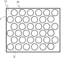
- FIG. 3 shows an aspect of the uneven portion provided on the crystal growth surface of the crystal substrate in the present invention.
- the uneven portion of FIG. 3 is composed of the crystal substrate 1 and the mask layer 4.
- FIG. 4 shows the surface of the uneven portion shown in FIG. 3 as viewed from the zenith direction.
- the mask layer 4 is formed on the crystal growth surface of the crystal substrate 1 and has holes in a dot shape.
- the crystal substrate 1 is exposed from the dot holes of the mask layer 4, and the dot-shaped recesses 2b are formed in a triangular lattice shape.
- the circles of the dots are provided at regular intervals a.
- the period a is not particularly limited, but in the present invention, it is preferably 1 ⁇ m to 1 mm, and more preferably 5 ⁇ m to 300 ⁇ m.
- the period a refers to the distance between the ends of circles of adjacent dots.
- the mask layer 4 can be formed by forming a film of the constituent material of the mask layer 4 and then processing it into a predetermined shape using a known means such as photolithography.
- the constituent material of the mask layer 4 include oxides such as Si, Ge, Ti, Zr, Hf, Ta, Sn, and Al, nitrides or carbides, carbon, diamond, metal, or a mixture thereof. Can be mentioned.
- the mask layer 4 preferably contains a metal oxide of a transition metal, more preferably contains a metal oxide of a Group 4 metal of the Periodic Table, and most preferably contains titanium oxide.
- the film forming means of the mask layer 4 is not particularly limited, and may be a known means. Examples of the means for forming the film of the constituent material of the mask layer 4 include a vacuum vapor deposition method, a CVD method, a sputtering method, and the like.
- the mask layer contains titanium oxide
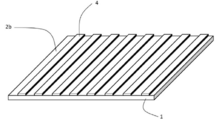
- FIG. 5 shows one aspect of the uneven portion provided on the crystal growth surface of the crystal substrate in the present invention.
- the uneven portion of FIG. 5 is composed of a crystal substrate 1 and a mask layer 4.
- the mask layer is formed in stripes on the crystal growth surface of the crystal substrate 1, and the recesses (grooves) 2b are formed in stripes by the mask layer 4.
- the mask layer 4 can be formed by using a known means such as photolithography.
- Examples of the constituent material of the mask layer 4 include oxides such as Si, Ge, Ti, Zr, Hf, Ta, Sn, and Al, nitrides or carbides, carbon, diamond, metal, or a mixture thereof. Can be mentioned.
- the mask layer 4 preferably contains a metal oxide of a transition metal, more preferably contains a metal oxide of a Group 4 metal of the Periodic Table, and most preferably contains titanium oxide.
- the constituent material of the mask layer such preferable, the crystallinity of the second crystal layer can be made more excellent.
- the width and height of the convex portion (mask layer) of the uneven portion, the width and depth of the concave portion, the interval, and the like are not particularly limited, but in the present invention, the width of the convex portion (mask layer) is about 1 ⁇ m to about 1 mm. It is preferably about 5 ⁇ m to about 300 ⁇ m, more preferably about 10 ⁇ m to about 100 ⁇ m.
- the height of the convex portion is preferably about 1 nm to about 10 ⁇ m, more preferably about 5 nm to about 1 ⁇ m, and more preferably about 10 nm to about 100 nm. Is the most preferable.
- the width of the recess is preferably about 1 ⁇ m to about 300 ⁇ m, more preferably about 3 ⁇ m to about 100 ⁇ m, and most preferably about 5 ⁇ m to about 50 ⁇ m.
- the depth of the recess is preferably about 1 nm to about 1 mm, more preferably about 10 nm to about 300 ⁇ m, and most preferably about 20 nm to about 100 ⁇ m.
- FIG. 2 shows a cross-sectional view of the crystalline laminated structure of the present invention.
- the first crystal layer 3 is formed on the crystal substrate 1, and the second crystal layer 5 is further formed by crystal growth.
- the first crystal layer 3 is provided with polycrystals 3a and single crystals 3b alternately adjacent to each other in the lateral direction.
- crystalline oxides are also grown laterally on the first crystal layer 3. In this way, by growing the second crystal layer 5 containing the single crystal of the crystalline oxide on the first crystal layer 3 containing polycrystals, the crystallinity of the second crystal layer 5 is further improved. Can be. Further, in the crystalline laminated structure of FIG.
- the polycrystals 3a and the single crystals 3b in the first crystal layer 3 are provided on the surface of the first crystal layer 3 and are alternately adjacent to each other in the lateral direction. Since it is provided, the second crystal layer 5 can be a high-quality crystal layer in which a well-continuous lateral growth portion is formed.
- a buffer layer including a stress relaxation layer or the like may be provided on the crystal substrate, and when the buffer layer is provided, the uneven portion may be formed on the buffer layer as well.
- the buffer layer may have crystallinity or may be amorphous, but it is preferable that the buffer layer has crystallinity.
- the buffer layer may be a single crystal layer or a polycrystalline layer. Further, the buffer layer may contain mixed crystals.
- the substrate has a buffer layer on a part or all of the surface.
- the means for forming the buffer layer is not particularly limited and may be a known means.
- the forming means include a spray method, a mist CVD method, an HVPE method, an MBE method, a MOCVD method, a sputtering method and the like.
- the buffer layer formed by the mist CVD method can improve the film quality of the crystal film formed on the buffer layer, and in particular, can cause crystal defects such as tilt. It is preferable because it can be suppressed.
- the means for forming the first crystal layer and the second crystal layer is not particularly limited and may be known means.
- the forming means include a CVD method, a MOCVD method, a MOVPE method, a mist CVD method, a mist epitaxy method, an MBE method, an HVPE method, a pulse growth method, an ALD method, a sputtering method and the like.
- the forming means is preferably a mist CVD method, a mist epitaxy method or an HVPE method, and more preferably an HVPE method.
- the means for forming the first crystal layer and the second crystal layer are the same, so that the first crystal layer and the second crystal layer can be continuously and efficiently formed. Therefore, it is preferable.
- the means for forming the stress relaxation layer and / or the crystalline oxide layer may be the same as the means for forming the first crystal layer and the second crystal layer.
- the present invention will be described in more detail by taking as an example the case where the HVPE method is used as a means for forming the first crystal layer or the second crystal layer (hereinafter, collectively referred to as “crystal layer”).
- a metal source containing a metal is gasified to obtain a metal halide gas, and then the metal halide gas and an oxygen-containing raw material gas are supplied to the crystal substrate in the reaction chamber. It is preferable that the reactive gas is supplied onto the crystal substrate and the film formation is carried out under the flow of the reactive gas.
- the metal source is not particularly limited as long as it contains a metal and can be gasified, and may be a simple substance of a metal or a metal compound.
- the metal include one or more metals selected from gallium, aluminum, indium, iron, chromium, vanadium, titanium, rhodium, nickel, cobalt, iridium and the like.
- the metal is preferably one or more metals selected from gallium, aluminum and indium, more preferably gallium, and the metal source is gallium alone. Most preferred.
- the metal source may be a gas, a liquid, or a solid, but in the present invention, for example, when gallium is used as the metal, the metal is used.
- the source is preferably a liquid.
- the gasification means is not particularly limited and may be a known means as long as the object of the present invention is not impaired.
- the gasification means is preferably carried out by halogenating the metal source.
- the halogenating agent used for the halogenation is not particularly limited as long as the metal source can be halogenated, and may be a known halogenating agent.
- the halogenating agent include halogens and hydrogen halides.
- the halogen include fluorine, chlorine, bromine, iodine and the like.
- hydrogen halide include hydrogen fluoride, hydrogen chloride, hydrogen bromide, hydrogen iodide and the like.
- the gasification is carried out by supplying halogen or hydrogen halide as a halogenating agent to the metal source and reacting the metal source with halogen or hydrogen halide at a temperature equal to or higher than the vaporization temperature of the metal halide. It is preferable to carry out the process by forming a metal halide.
- the halogenation reaction temperature is not particularly limited, but in the present invention, for example, when the metal source is gallium and the halogenating agent is HCl, 900 ° C. or lower is preferable, and 700 ° C. or lower is preferable.
- the metal halide gas is not particularly limited as long as it is a gas containing a halide of the metal of the metal source.
- the metal halide gas include halides of the metal (fluoride, chloride, bromide, iodide, etc.).
- the metal halide gas and the oxygen-containing raw material gas are supplied onto a substrate in the reaction chamber. Further, in the present invention, the reactive gas is supplied onto the substrate.
- the formation temperature of the crystal layer is not particularly limited, but in the present invention, for example, when the metal source is gallium and the halogenating agent is HCl, the temperature is preferably 900 ° C. or lower, preferably 700 ° C. or lower. Is more preferable, and the temperature is most preferably 400 ° C. to 700 ° C.
- the first crystal layer is formed at a low temperature (for example, less than 500 ° C.) and the second crystal layer is formed at a high temperature (for example, 500 ° C. or higher). It is preferable because the crystal layer and the second crystal layer can be made separately.
- the oxygen-containing raw material gas may be, for example, one or more gases selected from O 2 gas, CO 2 gas, NO gas, NO 2 gas, N 2 O gas, H 2 O gas or O 3 gas. is there.
- the reactive gas is usually a reactive gas different from the metal halide gas and the oxygen-containing raw material gas, and does not include an inert gas.
- the reactive gas is not particularly limited, and examples thereof include an etching gas and the like.
- the etching gas is not particularly limited and may be a known etching gas as long as the object of the present invention is not impaired.
- the reactive gas is a halogen gas (for example, fluorine gas, chlorine gas, bromine gas, iodine gas, etc.), hydrogen halide gas (for example, hydrofluoric acid gas, hydrochloric acid gas, hydrogen bromide gas, or hydrogen bromide gas).
- the metal halide gas, the oxygen-containing raw material gas, and the reactive gas may contain a carrier gas.
- the carrier gas include an inert gas such as nitrogen and argon.
- the partial pressure of the metal halide gas is not particularly limited, but in the present invention, it is preferably 0.5 Pa to 1 kPa, and more preferably 5 Pa to 0.5 kPa.
- the partial pressure of the oxygen-containing raw material gas is not particularly limited, but in the present invention, it is preferably 0.5 to 100 times the partial pressure of the metal halide gas, and 1 to 20 times the partial pressure. Is more preferable.
- the partial pressure of the reactive gas is also not particularly limited, but in the present invention, it is preferably 0.1 to 5 times, preferably 0.2 to 3 times, the partial pressure of the metal halide gas. Is more preferable.
- the dopant-containing raw material gas is not particularly limited as long as it contains a dopant.
- the dopant is also not particularly limited, but in the present invention, the dopant preferably contains one or more elements selected from germanium, silicon, titanium, zirconium, vanadium, niobium and tin, preferably germanium. It is more preferably containing silicon or tin, and most preferably it contains germanium.
- the dopant-containing raw material gas preferably has the dopant in the form of a compound (for example, a halide, an oxide, etc.), and more preferably in the form of a halide.
- the partial pressure of the dopant-containing raw material gas is not particularly limited, but in the present invention, it is preferably 1 ⁇ 10 -7 times to 0.1 times the partial pressure of the metal-containing raw material gas, and is 2.5 ⁇ . More preferably, it is 10-6 times to 7.5 ⁇ 10-2 times. In the present invention, it is preferable to supply the dopant-containing raw material gas together with the reactive gas onto the substrate.
- the stress relaxation layer is not particularly limited as long as it contains a polycrystal containing an oxide represented by M 2 O 3 (in the formula, M represents a trivalent metal atom and O represents an oxygen atom).
- M represents a trivalent metal atom
- O represents an oxygen atom
- the trivalent metal atom include aluminum (Al), gallium (Ga), indium (In), thallium (Tl), cobalt (Co), rhodium (Rh), iridium (Ir), and iron (Fe).
- the trivalent metal atom preferably contains a Group 13 metal of the Periodic Table, and more preferably gallium.
- the "main component” means, for example, when the polycrystal contains Ga 2 O 3 as a main component, the atomic ratio of gallium in the metal element in the polycrystal is 0.5 or more, and Ga 2 is used. If O 3 is included, that is sufficient.
- the atomic ratio of gallium in the metal element in the polycrystal is preferably 0.7 or more, more preferably 0.8 or more.
- the polycrystal may contain a mixed crystal, in which case, for example, the polycrystal may contain gallium and aluminum, indium, iron, chromium, vanadium, titanium, rhodium, nickel, cobalt and It preferably contains one or more metals selected from iridium.
- the crystal structure of the polycrystal is not particularly limited as long as the object of the present invention is not impaired.
- the crystal structure of the polycrystal includes, for example, a corundum structure, a ⁇ -gallia structure, a hexagonal structure (for example, ⁇ -type structure, etc.), a rectangular structure (for example, a ⁇ -type structure, etc.), a cubic structure, or a tetragonal crystal.
- the polycrystal preferably has a corundum structure, a ⁇ -Galia structure, a hexagonal structure (for example, ⁇ -type structure, etc.) or an orthorhombic structure (for example, ⁇ -type structure, etc.). It is more preferable to have (for example, a ⁇ type structure).
- the stress relaxation layer further contains a single crystal because the crystalline oxide layer formed on the stress relaxation layer can have higher quality.
- the constituent material of the single crystal is also not particularly limited as long as the object of the present invention is not impaired.
- the constituent material of the single crystal for example, a single metal oxide containing one or more metals selected from aluminum, gallium, indium, iron, chromium, vanadium, titanium, rhodium, nickel, cobalt and iridium.
- the single crystal preferably contains a single crystal of a metal oxide of at least one metal selected from aluminum, indium and gallium, and at least a single crystal of a metal oxide of a metal containing gallium. Is more preferable, and it is most preferable to contain single crystal gallium oxide or a mixed crystal thereof.
- the crystal structure of the single crystal is not particularly limited as long as the object of the present invention is not impaired.
- the crystal structure of the single crystal includes, for example, a corundum structure, a ⁇ -gallia structure, a hexagonal structure (for example, ⁇ -type structure, etc.), a rectangular structure (for example, a ⁇ -type structure, etc.), a cubic structure, or a tetragonal structure. And so on.
- the single crystal preferably has a corundum structure, a ⁇ -Galia structure hexagonal structure (for example, ⁇ -type structure, etc.) or an orthorhombic structure (for example, ⁇ -type structure, etc.), and has a corundum structure. Is more preferable.
- the thickness of the stress relaxation layer is not particularly limited and may be 1 ⁇ m or more or 1 ⁇ m or less.
- the stress relaxation layer may include an amorphous portion. Further, in the embodiment of the present invention, it is preferable that the stress relaxation layer has voids because the crystalline oxide layer can be made of higher quality.
- the stress relaxation layer of such a preferable embodiment can be obtained by appropriately adjusting conditions such as growth rate in the method of forming the stress relaxation layer.
- the polycrystal and the single crystal in the stress relaxation layer are provided adjacent to each other in the lateral direction, so that the lateral growth portion is better formed in the crystalline oxide layer. Therefore, it is preferable that they are provided alternately adjacent to each other in the lateral direction, and it is most preferable that the polycrystal and the single crystal are provided at least on the surface of the stress relaxation layer.
- the planar shape of the single crystal and / or the polycrystal is also not particularly limited, but in the present invention, it may be striped, island-shaped, rectangular or lattice-shaped (square lattice, oblique lattice, triangular lattice, hexagonal lattice). It is preferably present, more preferably striped or grid-like, and most preferably grid-like.
- the stress relaxation layer having a concave-convex portion or a convex portion formed on at least a part of the surface thereof is laminated as the stress relaxation layer to further improve the quality of the crystalline oxide layer. It is preferable because it can be used.
- Such a stress relaxation layer is formed, for example, by forming the uneven portion on the surface of the crystal substrate and then forming the stress relaxation layer on the uneven portion by using the above-mentioned preferable forming means. It can be preferably performed.
- the shape of the concavo-convex portion of the stress relaxation layer may be the same as the shape of the concavo-convex portion on the crystal substrate described above.
- the crystalline oxide layer is not particularly limited as long as it contains a single crystal of the crystalline oxide, but in the present invention, it is preferable to contain the single crystal of the crystalline oxide as a main component.
- the crystalline oxide may be a semiconductor.
- the crystalline oxide include crystals of a metal oxide containing one or more metals selected from aluminum, gallium, indium, iron, chromium, vanadium, titanium, rhodium, nickel, cobalt and iridium. Can be mentioned.
- the crystalline oxide preferably contains at least one metal selected from aluminum, indium and gallium, more preferably at least gallium, in crystalline gallium oxide or a mixed crystal thereof. Most preferably.
- the crystal structure of the crystalline oxide is not particularly limited.
- the crystal structure of the crystalline oxide includes, for example, a corundum structure, a ⁇ -gallia structure, a hexagonal structure (for example, ⁇ -type structure, etc.), an orthorhombic structure (for example, a ⁇ -type structure, etc.), a cubic structure, or a tetragonal structure.
- a crystal structure and the like can be mentioned.
- the crystalline oxide preferably has a corundum structure, a ⁇ -gaul structure or a hexagonal crystal (for example, an ⁇ -type structure), and more preferably has a corundum structure.
- the quality such as crystallinity of the crystalline oxide layer can be made more excellent.
- the "main component” is preferably 50% or more, more preferably 70% or more, still more preferably 90%, based on the atomic ratio of the crystalline oxide with respect to all the components of the crystalline oxide layer. It means that the above is included, and it means that it may be 100%.
- the thickness of the crystalline oxide layer is not particularly limited, but is preferably 10 ⁇ m or more, more preferably 30 ⁇ m or more, and most preferably 50 ⁇ m or more. Further, in the present invention, it is preferable that the crystalline oxide layer includes a lateral growth portion.
- the lateral growth portion is not particularly limited as long as it is a portion that grows in the lateral direction or substantially lateral direction with respect to the thickness direction of the crystalline oxide layer.
- the stress relaxation layer contains a single crystal
- the crystal structure of the crystalline oxide and the crystal structure of the single crystal in the stress relaxation layer are the same, that is, the crystallinity oxidation. Since the crystallinity of the laterally growing portion of the material layer can be made more excellent, it is preferable that the crystalline oxide and the constituent material of the single crystal in the stress relaxation layer are the same. preferable.
- the crystalline oxide layer may contain a dopant.
- the dopant is not particularly limited and may be a known one, and may be an n-type dopant or a p-type dopant.
- Examples of the n-type dopant include tin, germanium, silicon, titanium, zirconium, vanadium, niobium, two or more of these elements, and the like.
- Examples of the p-type dopant include Mg, H, Li, Na, K, Rb, Cs, Fr, Be, Ca, Sr, Ba, Ra, Mn, Fe, Co, Ni, Pd, Cu, Ag and Au. , Zn, Cd, Hg, Ti, Pb, N, P or two or more of these elements.
- the content of the dopant is also not particularly limited, but is preferably 0.00001 atomic% or more, more preferably 0.00001 atomic% to 20 atomic%, and 0. Most preferably, it is 0.001 atomic% to 10 atomic%.
- the crystalline laminated structure of the present invention can be particularly suitably used for semiconductor devices, and is particularly useful for power devices.
- Semiconductor devices formed using the crystalline laminated structure include transistors and TFTs such as MIS, HEMT, and MOS, Schottky barrier diodes using semiconductor-metal junctions, and PN or PIN combined with other P layers. Examples include diodes and light emitting / receiving elements.
- the crystalline laminated structure may be used as it is in a semiconductor device or the like, or the crystal substrate and / or the first crystal layer and the second crystal layer may be peeled off by a known means. It may be applied to a semiconductor device or the like.
- the semiconductor device of the present invention is suitably used as a power module, an inverter or a converter by using known means, and these semiconductor devices are also included in the present invention. Further, the semiconductor device of the present invention is further preferably used for, for example, a semiconductor system using a power supply device.
- the power supply device can be manufactured from or as the semiconductor device by connecting to a wiring pattern or the like using a known means.
- FIG. 10 shows an example of a power supply system.
- a power supply system is configured by using the plurality of power supply devices and control circuits. As shown in FIG. 11, the power supply system can be used in a system device in combination with an electronic circuit.
- An example of the power supply circuit diagram of the power supply device is shown in FIG. FIG.
- a DC voltage is switched at a high frequency by an inverter (MOSFET: composed of A to D), converted to AC, and then insulated and transformed by a transformer. This is performed, rectified by a rectifying MOSFET (A to B'), smoothed by a DCL (smoothing coils L1 and L2) and a capacitor, and a DC voltage is output. At this time, the output voltage is compared with the reference voltage by the voltage comparator, and the inverter and the rectifying MOSFET are controlled by the PWM control circuit so as to obtain the desired output voltage.
- MOSFET composed of A to D
- Example 1 Mask formation A sapphire substrate (c-plane, off-angle 0.25 °) having an ⁇ -Ga 2 O 3 layer formed on its surface is used as the substrate, and a mask layer made of titanium oxide is used on the substrate by a sputtering method. Then, using a photolithography method, the formed mask layer was processed into a mask having a predetermined shape. In the sputtering method, a mask layer (thickness 50 nm) made of titanium oxide was formed by using a Ti target while flowing O 2 gas.
- the openings (dots) are arranged on the substrate in a triangular lattice pattern with a period (distance between the ends of adjacent dots) of 20 ⁇ m.
- the mask layer was processed.
- the halide vapor deposition (HVPE) device 50 used in this embodiment will be described with reference to FIG.
- the HVPE apparatus 50 includes a reaction chamber 51, a heater 52a for heating the metal source 57, and a heater 52b for heating the substrate fixed to the substrate holder 56, and further supplies an oxygen-containing raw material gas into the reaction chamber 51. It includes a pipe 55b, a reactive gas supply pipe 54b, and a board holder 56 on which a board is installed.
- a metal-containing raw material gas (metal halide gas) supply pipe 53b is provided in the reactive gas supply pipe 54b to form a double pipe structure.
- the oxygen-containing raw material gas supply pipe 55b is connected to the oxygen-containing raw material gas supply source 55a, and the oxygen-containing raw material gas is transferred from the oxygen-containing raw material gas supply source 55a via the oxygen-containing raw material gas supply pipe 55b to the substrate holder.
- the flow path of the oxygen-containing raw material gas is configured so that it can be supplied to the substrate fixed to 56.
- the reactive gas supply pipe 54b is connected to the reactive gas supply source 54a, and the reactive gas is fixed to the substrate holder 56 from the reactive gas supply source 54a via the reactive gas supply pipe 54b.
- the flow path of the reactive gas is configured so that it can be supplied to the substrate.
- the metal-containing raw material gas supply pipe 53b is connected to the halogen-containing raw material gas supply source 53a, and the halogen-containing raw material gas is supplied to the metal source to become the metal-containing raw material gas, and the metal-containing raw material gas is fixed to the substrate holder 56. It is supplied to the substrate.
- the reaction chamber 51 is provided with a gas discharge unit 59 for exhausting used gas, and further, a protective sheet 58 for preventing precipitation of reactants is provided on the inner wall of the reaction chamber 51.
- a gallium (Ga) metal source 57 (purity 99.99999% or more) is arranged inside the metal-containing raw material gas supply pipe 53b, and the above 1.
- the sapphire substrate with the mask layer obtained in the above was installed.
- the heaters 52a and 52b were operated to raise the temperature in the reaction chamber 51 to 570 ° C (near the Ga metal source) and 540 ° C (near the substrate holder).
- Hydrogen chloride (HCl) gas (purity 99.999% or more) was supplied from the halogen-containing raw material gas supply source 53a to the gallium (Ga) metal 57 arranged inside the film-forming metal raw material-containing gas supply pipe 53b.
- Gallium chloride (GaCl / GaCl 3 ) was produced by a chemical reaction between a Ga metal and hydrogen chloride (HCl) gas.
- the obtained gallium chloride (GaCl / GaCl 3 ) and O 2 gas (purity 99.99995% or more) supplied from the oxygen-containing raw material gas supply source 55a are supplied onto the substrate through the reactive gas supply pipe 54b. did.
- the flow rate of the HCl gas supplied from the halogen-containing raw material gas supply source 53a is 10 sccm
- the flow rate of the HCl gas supplied from the reactive gas supply source 54a is 10 sccm
- the flow rate of the HCl gas supplied from the oxygen-containing raw material gas supply source 55a is O.
- the flow rates of the two gases were maintained at 100 sccm, respectively.
- FIGS. 6 and 7 show an SEM image of the laminated structure after 60 minutes of film formation
- FIG. 7 shows an SEM image of the laminated structure after 120 minutes of film formation
- 7 (a) shows a bird's-eye view
- FIG. 7 (b) shows a cross-sectional view. From the SEM observation results of FIGS. 6 and 7 and the analysis results using the XRD diffractometer, polycrystals containing k-Ga 2 O 3 and ⁇ -Ga 2 O 3 single crystals are alternately adjacent to each other on a mask made of titanium oxide.
- the ⁇ -Ga 2 O 3 single crystal (second crystal) was grown in the vertical direction and the horizontal direction. Further, even when the film was formed for a long time, the crystal film did not peel off from the substrate, and a high-quality ⁇ -Ga 2 O 3 single crystal was formed. Further, when the film formation was further continued on the laminated structure shown in FIG. 7, the lateral growth portions were associated with each other, and a high-quality single crystal layer (second crystal layer) having a continuous lateral growth portion was formed. Was found to be formed.
- Example 1 A laminated structure was produced in the same manner as in Example 1 except that SiO 2 was used as the mask material. The obtained laminated structure was observed by SEM. The results are shown in FIG. From the SEM observation result of FIG. 8 and the analysis result using the XRD diffractometer , an amorphous portion was formed on the SiO 2 mask, and a part of the amorphous portion grew abnormally and ⁇ -Ga 2 O. It was found that 3 was formed.
- Example 2 In the formation of the titanium oxide mask layer by the sputtering method, a laminated structure was produced in the same manner as in Example 1 except that the thickness of the titanium oxide layer was set to 10 nm. The obtained laminated structure was observed by SEM.
- the SEM image of the laminated structure after the film formation is shown in FIG. 9 (a) shows a bird's-eye view, and FIG. 9 (b) shows a cross-sectional view. From the SEM observation result of FIG. 9 and the analysis result using the XRD diffractometer, a ⁇ -Ga 2 O 3 single crystal layer was formed on the titanium oxide mask, and an ⁇ -Ga 2 O 3 layer was formed on the single crystal layer. It was found that (second crystal layer) was formed. Further, with respect to the laminated structure shown in FIG. 9, when the film formation was continued for 120 minutes and then the film formation was continued, the crystal layer was peeled off from the substrate and the film could not be further thickened.
- Comparative Example 3 A laminated structure was produced in the same manner as in Example 1 except that an alumina (Al 2 O 3 ) mask layer was used instead of the titanium oxide mask layer. As a result, as in the case of Comparative Example 1, an amorphous portion is formed on the mask and abnormal growth occurs, and if the growth is continued, the crystal layer is peeled off from the substrate and the film cannot be thickened. It was.
- an alumina (Al 2 O 3 ) mask layer was used instead of the titanium oxide mask layer.
- Example 2 A laminated structure was obtained in the same manner as in Example 1 except that the first crystal layer was formed so that the mask width was 10 ⁇ m and at least a part of the first crystal layer had voids. It was. More specifically, by first growing at a growth temperature of 520 ° C. for 20 minutes, then lowering the growth temperature to 460 ° C. and growing for another 40 minutes, the polycrystalline k-Ga 2 O 3 having a void structure is masked. Accumulated on top. The obtained laminated structure was observed by SEM. The results are shown in FIG. From the SEM observation result of FIG.
- the crystalline laminated structure and semiconductor device of the present invention can be used in all fields such as semiconductors (for example, compound semiconductor electronic devices, etc.), electronic parts / electrical equipment parts, optical / electrophotographic-related equipment, industrial parts, etc. , Useful for manufacturing semiconductor devices and the like.
- semiconductors for example, compound semiconductor electronic devices, etc.
- electronic parts / electrical equipment parts for example, electronic parts / electrical equipment parts
- optical / electrophotographic-related equipment for manufacturing semiconductor devices and the like.
Landscapes
- Chemical & Material Sciences (AREA)
- Engineering & Computer Science (AREA)
- Crystallography & Structural Chemistry (AREA)
- Materials Engineering (AREA)
- Metallurgy (AREA)
- Organic Chemistry (AREA)
- Inorganic Chemistry (AREA)
- Chemical Kinetics & Catalysis (AREA)
- General Chemical & Material Sciences (AREA)
- Crystals, And After-Treatments Of Crystals (AREA)
- Chemical Vapour Deposition (AREA)
Priority Applications (1)
| Application Number | Priority Date | Filing Date | Title |
|---|---|---|---|
| JP2021551489A JPWO2021066156A1 (https=) | 2019-10-04 | 2020-10-02 |
Applications Claiming Priority (4)
| Application Number | Priority Date | Filing Date | Title |
|---|---|---|---|
| JP2019183939 | 2019-10-04 | ||
| JP2019-183939 | 2019-10-04 | ||
| JP2019-183940 | 2019-10-04 | ||
| JP2019183940 | 2019-10-04 |
Publications (1)
| Publication Number | Publication Date |
|---|---|
| WO2021066156A1 true WO2021066156A1 (ja) | 2021-04-08 |
Family
ID=75338098
Family Applications (1)
| Application Number | Title | Priority Date | Filing Date |
|---|---|---|---|
| PCT/JP2020/037577 Ceased WO2021066156A1 (ja) | 2019-10-04 | 2020-10-02 | 結晶性積層構造体および半導体装置 |
Country Status (2)
| Country | Link |
|---|---|
| JP (1) | JPWO2021066156A1 (https=) |
| WO (1) | WO2021066156A1 (https=) |
Cited By (1)
| Publication number | Priority date | Publication date | Assignee | Title |
|---|---|---|---|---|
| EP4431634A4 (en) * | 2021-11-10 | 2025-10-29 | Shinetsu Chemical Co | BASE SUBSTRATE, MULTILAYER MONOCRYSTALLINE DIAMOND SUBSTRATE, PROCESS FOR PRODUCING BASE SUBSTRATE, AND PROCESS FOR PRODUCING MULTILAYER MONOCRYSTALLINE DIAMOND SUBSTRATE |
Citations (3)
| Publication number | Priority date | Publication date | Assignee | Title |
|---|---|---|---|---|
| JPS645999A (en) * | 1987-06-29 | 1989-01-10 | Nippon Telegraph & Telephone | Production of thin film of ferroelectric single crystal |
| JP2016025256A (ja) * | 2014-07-22 | 2016-02-08 | 株式会社Flosfia | 半導体装置 |
| JP2018002544A (ja) * | 2016-06-30 | 2018-01-11 | 株式会社Flosfia | 結晶性酸化物半導体膜およびその製造方法 |
-
2020
- 2020-10-02 JP JP2021551489A patent/JPWO2021066156A1/ja active Pending
- 2020-10-02 WO PCT/JP2020/037577 patent/WO2021066156A1/ja not_active Ceased
Patent Citations (3)
| Publication number | Priority date | Publication date | Assignee | Title |
|---|---|---|---|---|
| JPS645999A (en) * | 1987-06-29 | 1989-01-10 | Nippon Telegraph & Telephone | Production of thin film of ferroelectric single crystal |
| JP2016025256A (ja) * | 2014-07-22 | 2016-02-08 | 株式会社Flosfia | 半導体装置 |
| JP2018002544A (ja) * | 2016-06-30 | 2018-01-11 | 株式会社Flosfia | 結晶性酸化物半導体膜およびその製造方法 |
Cited By (1)
| Publication number | Priority date | Publication date | Assignee | Title |
|---|---|---|---|---|
| EP4431634A4 (en) * | 2021-11-10 | 2025-10-29 | Shinetsu Chemical Co | BASE SUBSTRATE, MULTILAYER MONOCRYSTALLINE DIAMOND SUBSTRATE, PROCESS FOR PRODUCING BASE SUBSTRATE, AND PROCESS FOR PRODUCING MULTILAYER MONOCRYSTALLINE DIAMOND SUBSTRATE |
Also Published As
| Publication number | Publication date |
|---|---|
| JPWO2021066156A1 (https=) | 2021-04-08 |
Similar Documents
| Publication | Publication Date | Title |
|---|---|---|
| JP7480937B2 (ja) | 結晶膜、半導体装置および結晶膜の製造方法 | |
| JP7460975B2 (ja) | 結晶膜の製造方法 | |
| JP7166522B2 (ja) | 結晶膜の製造方法 | |
| JP7163540B2 (ja) | 結晶膜の製造方法 | |
| JP7648034B2 (ja) | 積層構造体および半導体装置 | |
| JP7741487B2 (ja) | 結晶性酸化物膜 | |
| JP7404593B2 (ja) | 成膜方法および結晶性積層構造体 | |
| JP7659153B2 (ja) | 結晶性積層構造体および半導体装置 | |
| US11804519B2 (en) | Crystalline multilayer structure, semiconductor device, and method of manufacturing crystalline structure | |
| WO2021066156A1 (ja) | 結晶性積層構造体および半導体装置 | |
| JP7530054B2 (ja) | 結晶膜の製造方法 | |
| US20220189769A1 (en) | Crystal film, semiconductor device including crystal film, and method of producing crystal film | |
| JP7649944B2 (ja) | 結晶性積層構造体の製造方法 | |
| US11694894B2 (en) | Crystalline film containing a crystalline metal oxide and method for manufacturing the same under partial pressure | |
| JP2025126924A (ja) | 結晶膜 | |
| JP7598113B2 (ja) | 結晶膜の成長方法および結晶性酸化物膜 | |
| WO2023048150A1 (ja) | 結晶膜の製造方法および結晶膜 | |
| JP7453609B2 (ja) | 剥離方法および結晶性酸化物膜の製造方法 | |
| JP7344426B2 (ja) | 結晶性積層構造体 |
Legal Events
| Date | Code | Title | Description |
|---|---|---|---|
| 121 | Ep: the epo has been informed by wipo that ep was designated in this application |
Ref document number: 20871326 Country of ref document: EP Kind code of ref document: A1 |
|
| ENP | Entry into the national phase |
Ref document number: 2021551489 Country of ref document: JP Kind code of ref document: A |
|
| NENP | Non-entry into the national phase |
Ref country code: DE |
|
| 122 | Ep: pct application non-entry in european phase |
Ref document number: 20871326 Country of ref document: EP Kind code of ref document: A1 |