WO2021039639A1 - 弾性波装置 - Google Patents
弾性波装置 Download PDFInfo
- Publication number
- WO2021039639A1 WO2021039639A1 PCT/JP2020/031658 JP2020031658W WO2021039639A1 WO 2021039639 A1 WO2021039639 A1 WO 2021039639A1 JP 2020031658 W JP2020031658 W JP 2020031658W WO 2021039639 A1 WO2021039639 A1 WO 2021039639A1
- Authority
- WO
- WIPO (PCT)
- Prior art keywords
- elastic wave
- wave resonator
- film
- edge regions
- wave device
- Prior art date
- Legal status (The legal status is an assumption and is not a legal conclusion. Google has not performed a legal analysis and makes no representation as to the accuracy of the status listed.)
- Ceased
Links
Images


Classifications
-
- H—ELECTRICITY
- H03—ELECTRONIC CIRCUITRY
- H03H—IMPEDANCE NETWORKS, e.g. RESONANT CIRCUITS; RESONATORS
- H03H9/00—Networks comprising electromechanical or electro-acoustic elements; Electromechanical resonators
- H03H9/02—Details
- H03H9/125—Driving means, e.g. electrodes, coils
- H03H9/145—Driving means, e.g. electrodes, coils for networks using surface acoustic waves
- H03H9/14538—Formation
- H03H9/14541—Multilayer finger or busbar electrode
-
- H—ELECTRICITY
- H03—ELECTRONIC CIRCUITRY
- H03H—IMPEDANCE NETWORKS, e.g. RESONANT CIRCUITS; RESONATORS
- H03H9/00—Networks comprising electromechanical or electro-acoustic elements; Electromechanical resonators
- H03H9/15—Constructional features of resonators consisting of piezoelectric or electrostrictive material
- H03H9/17—Constructional features of resonators consisting of piezoelectric or electrostrictive material having a single resonator
-
- H—ELECTRICITY
- H03—ELECTRONIC CIRCUITRY
- H03H—IMPEDANCE NETWORKS, e.g. RESONANT CIRCUITS; RESONATORS
- H03H9/00—Networks comprising electromechanical or electro-acoustic elements; Electromechanical resonators
- H03H9/46—Filters
- H03H9/64—Filters using surface acoustic waves
- H03H9/6423—Means for obtaining a particular transfer characteristic
- H03H9/6433—Coupled resonator filters
- H03H9/6436—Coupled resonator filters having one acoustic track only
-
- H—ELECTRICITY
- H03—ELECTRONIC CIRCUITRY
- H03H—IMPEDANCE NETWORKS, e.g. RESONANT CIRCUITS; RESONATORS
- H03H9/00—Networks comprising electromechanical or electro-acoustic elements; Electromechanical resonators
- H03H9/02—Details
- H03H9/02535—Details of surface acoustic wave devices
- H03H9/02543—Characteristics of substrate, e.g. cutting angles
- H03H9/02574—Characteristics of substrate, e.g. cutting angles of combined substrates, multilayered substrates, piezoelectrical layers on not-piezoelectrical substrate
-
- H—ELECTRICITY
- H03—ELECTRONIC CIRCUITRY
- H03H—IMPEDANCE NETWORKS, e.g. RESONANT CIRCUITS; RESONATORS
- H03H9/00—Networks comprising electromechanical or electro-acoustic elements; Electromechanical resonators
- H03H9/02—Details
- H03H9/02535—Details of surface acoustic wave devices
- H03H9/02992—Details of bus bars, contact pads or other electrical connections for finger electrodes
-
- H—ELECTRICITY
- H03—ELECTRONIC CIRCUITRY
- H03H—IMPEDANCE NETWORKS, e.g. RESONANT CIRCUITS; RESONATORS
- H03H9/00—Networks comprising electromechanical or electro-acoustic elements; Electromechanical resonators
- H03H9/02—Details
- H03H9/125—Driving means, e.g. electrodes, coils
- H03H9/13—Driving means, e.g. electrodes, coils for networks consisting of piezoelectric or electrostrictive materials
-
- H—ELECTRICITY
- H03—ELECTRONIC CIRCUITRY
- H03H—IMPEDANCE NETWORKS, e.g. RESONANT CIRCUITS; RESONATORS
- H03H9/00—Networks comprising electromechanical or electro-acoustic elements; Electromechanical resonators
- H03H9/02—Details
- H03H9/125—Driving means, e.g. electrodes, coils
- H03H9/145—Driving means, e.g. electrodes, coils for networks using surface acoustic waves
- H03H9/14544—Transducers of particular shape or position
- H03H9/1457—Transducers having different finger widths
-
- H—ELECTRICITY
- H03—ELECTRONIC CIRCUITRY
- H03H—IMPEDANCE NETWORKS, e.g. RESONANT CIRCUITS; RESONATORS
- H03H9/00—Networks comprising electromechanical or electro-acoustic elements; Electromechanical resonators
- H03H9/25—Constructional features of resonators using surface acoustic waves
-
- H—ELECTRICITY
- H03—ELECTRONIC CIRCUITRY
- H03H—IMPEDANCE NETWORKS, e.g. RESONANT CIRCUITS; RESONATORS
- H03H9/00—Networks comprising electromechanical or electro-acoustic elements; Electromechanical resonators
- H03H9/46—Filters
- H03H9/64—Filters using surface acoustic waves
- H03H9/6423—Means for obtaining a particular transfer characteristic
- H03H9/6433—Coupled resonator filters
- H03H9/6483—Ladder SAW filters
Definitions
- the present invention relates to an elastic wave device having a structure in which first and second edge regions as low sound velocity regions are provided at both ends in a crossing region.
- a piston mode is formed to suppress transverse mode ripple. More specifically, in the IDT electrode, a region where adjacent electrode fingers overlap in the elastic wave propagation direction is defined as a crossing region.
- the crossing region has a central region and first and second edge regions arranged outside in the extending direction of the electrode fingers in the central region. The speed of sound in the first and second edge regions is lower than the speed of sound in the central region. Then, a region having a higher sound velocity than the central region is provided outside the first and second edge regions. Thereby, the piston mode is formed.
- transverse mode ripple is suppressed by forming a piston mode.
- the first and second edge regions are formed in both the elastic wave resonator and the vertically coupled elastic wave resonator filter.
- the lateral mode may not be sufficiently suppressed.
- An object of the present invention is to provide an elastic wave apparatus having an elastic wave resonator and a vertically coupled elastic wave resonator filter, which can suppress transverse mode more effectively. It is in.
- the elastic wave device is a vertically coupled type having an elastic wave resonator having an IDT electrode and a second piezoelectric substrate, which is composed of a first piezoelectric substrate and has a plurality of IDT electrodes.
- the IDT electrode of the elastic wave resonator and the IDT electrode of the vertically coupled elastic wave resonator filter are each provided with an elastic wave resonator filter, and each of the electrode fingers has a plurality of electrode fingers. It has crossing regions that intersect in the elastic wave propagation direction, and the crossing regions are provided on both outer sides of the central region and the central region in the direction in which the electrode finger extends, and the sound velocity is higher than that of the central region.
- the first and second edge regions have lower first and second edge regions, are arranged outside the extending direction of the electrode fingers in the first and second edge regions, and have a higher sound velocity than the central region.
- the first and second edge regions of the vertical coupling type elastic wave resonator filter are provided with a gap region of the above, and when the dimension along the extending direction of the electrode finger is defined as the length in the first and second edge regions.
- the length of the second edge region is shorter than the length of the first and second edge regions in the elastic wave resonator.
- the transverse mode can be effectively suppressed in both the elastic wave resonator and the vertically coupled elastic wave resonator filter.
- FIG. 1 is a circuit diagram of an elastic wave device according to a first embodiment of the present invention.
- FIG. 2 is a front sectional view for explaining the structure of an elastic wave resonator in the elastic wave device according to the first embodiment of the present invention.
- FIG. 3 is a schematic plan view for explaining the electrode arrangement of the elastic wave resonator in the elastic wave device according to the first embodiment of the present invention.
- FIG. 4 is a plan view showing the IDT electrode of the elastic wave resonator in the elastic wave device according to the first embodiment of the present invention.
- FIG. 5 is a partially cutaway plan view showing an enlarged main part of the IDT electrode shown in FIG. FIG.
- FIG. 6 is a schematic plan view for explaining the electrode arrangement of the vertically coupled elastic wave resonator filter in the elastic wave device according to the first embodiment of the present invention.
- 7 (a) and 7 (b) show the main part of the IDT electrode of the elastic wave resonator of the elastic wave apparatus and the main part of the IDT electrode of the vertical coupling type elastic wave resonator filter according to the first embodiment. It is a top view of each partial notch shown.
- FIG. 8A is a diagram showing the impedance characteristics of the elastic wave resonator in the elastic wave apparatus according to the first embodiment
- FIG. 8B is a diagram showing the S11 characteristics.
- FIG. 9 is a diagram showing the relationship between the lengths of the first and second edge regions of the elastic wave resonator in the elastic wave apparatus according to the first embodiment and the ripple intensity which is the intensity of the transverse mode ripple.
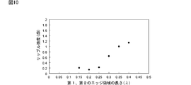
- FIG. 10 is a diagram showing the relationship between the lengths of the first and second edge regions of the vertically coupled elastic wave resonator filter in Example 1 and the ripple intensity, which is the intensity of the transverse mode ripple.
- FIG. 11 is a diagram showing the relationship between the lengths of the first and second edge regions of the elastic wave resonator in the elastic wave apparatus of Example 2 using the LiNbO 3 film and the ripple intensity which is the intensity of the transverse mode ripple. Is. FIG.
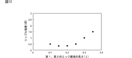
- FIG. 12 is a diagram showing the relationship between the lengths of the first and second edge regions of the vertically coupled elastic wave resonator filter in Example 2 using the LiNbO 3 film and the ripple intensity which is the intensity of the transverse mode ripple.
- FIG. 13 is a circuit diagram of an elastic wave device according to a second embodiment of the present invention.
- FIG. 14 is a plan view for explaining a modified example of the IDT electrode in the elastic wave device according to the second embodiment of the present invention.
- FIG. 15 is a plan view for explaining still another modification of the IDT electrode in the elastic wave device according to the second embodiment of the present invention.
- FIG. 1 is a circuit diagram of an elastic wave device according to a first embodiment of the present invention.
- the elastic wave device 1 is a duplexer and has a reception filter 2 and a transmission filter 3. One end of the reception filter 2 and the transmission filter 3 is connected to the antenna terminal 4.
- the reception filter 2 and the transmission filter 3 are each an elastic wave filter.
- a 1-port type elastic wave resonator 5 is connected in series with the vertically coupled elastic wave resonator filter 6.
- the transmission filter 3 has a plurality of series arm resonators S1 to S3 and a plurality of parallel arm resonators P1 and P2.
- the series arm resonators S1 to S3 and the parallel arm resonators P1 and P2 are each composed of a 1-port elastic wave resonator. That is, the transmission filter 3 is a ladder type filter having a plurality of elastic wave resonators.
- first and second edge regions are provided in the intersecting region of the IDT electrodes. ..
- the lengths of the first and second edge regions are different between the elastic wave resonator 5 and the vertically coupled elastic wave resonator filter 6. Thereby, the transverse mode can be suppressed more effectively.
- the structures of the elastic wave resonator 5 and the vertically coupled elastic wave resonator filter 6 will be described in more detail.
- FIG. 2 is a front sectional view for explaining the structure of the elastic wave resonator 5.
- the IDT electrode 16 and the reflectors 17 and 18 are provided on the first piezoelectric substrate 15.
- FIG. 3 is a schematic plan view showing a portion where the IDT electrode 16 and the reflectors 17 and 18 are provided. Reflectors 17 and 18 are provided on both sides of the IDT electrode 16 in the elastic wave propagation direction, thereby forming a 1-port elastic wave resonator.
- the support substrate 11 As shown in FIG. 2, in the first piezoelectric substrate 15, the support substrate 11, the hypersonic film 12 as the hypersonic material layer, the low sound velocity film 13 as the low sound velocity material layer, and the piezoelectric film 14 are in this order. It is laminated.
- the IDT electrode 16 is laminated on the piezoelectric film 14.
- the piezoelectric film 14 is made of a lithium tantalate single crystal film.
- the support substrate 11 is made of a semiconductor such as Si or SiC or an insulator such as aluminum oxide or quartz.
- the material of the support substrate 11 is not particularly limited.
- the hypersonic film 12 is made of a hypersonic material.
- the bass velocity film 13 is made of a bass velocity material.
- the hypersonic material is a material in which the sound velocity of the propagating bulk wave is higher than the sound velocity of the elastic wave propagating in the piezoelectric film 14.
- high-frequency materials include aluminum oxide, silicon carbide, silicon nitride, silicon nitride, silicon, sapphire, lithium tantalate, lithium niobate, crystal, alumina, zirconia, cozylite, mulite, steatite, and fol.
- Various materials such as sterite, magnesia, DLC (diamond-like carbon) film or diamond, a medium containing the above materials as a main component, and a medium containing a mixture of the above materials as a main component can be used.
- the low sound velocity material refers to a material in which the sound velocity of the propagating bulk wave is lower than the sound velocity of the bulk wave propagating through the piezoelectric film 14.
- Examples of such a low sound velocity material include silicon oxide, glass, silicon nitride, tantalum oxide, a compound obtained by adding fluorine, carbon, boron, hydrogen, or a silanol group to silicon oxide, and a medium containing the above material as a main component.
- Various materials such as can be used.
- the hypersonic material layer may also serve as a support substrate.
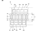
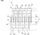
- FIG. 4 is a plan view showing the IDT electrode 16 of the elastic wave resonator 5
- FIG. 5 is a partially cutaway plan view showing a main part of FIG. 4 in an enlarged manner.
- the IDT electrode 16 has a plurality of first electrode fingers 21 and a plurality of second electrode fingers 22.
- the plurality of first electrode fingers 21 and the plurality of second electrode fingers 22 are interleaved with each other.
- the base end of the first electrode finger 21 is connected to the first bus bar 23.
- a plurality of openings 23c arranged along the elastic wave propagation direction are formed in the first bus bar 23.
- the portion of the opening 23c on the crossing region side, which will be described later, is the inner bus bar portion 23a.
- the region outside the crossing width direction of the opening 23c is the outer bus bar portion 23b.
- the connecting portion 23d is located at a portion where the first electrode finger 21 is extended.
- the connecting portion 23d connects the inner bus bar portion 23a and the outer bus bar portion 23b.
- the base end of the second electrode finger 22 is connected to the second bus bar 24.
- the second bus bar 24 is configured in the same manner as the first bus bar 23. That is, the second bus bar 24 has an inner bus bar portion 24a, an outer bus bar portion 24b, a plurality of openings 24c, and a plurality of connecting portions 24d.
- the inner bus bar portions 23a and 24a, the outer bus bar portions 23b and 24b, and the openings 23c and 24c may not be formed on the first bus bar 23 and the second bus bar 24.
- the region where the first electrode finger 21 and the second electrode finger 22 overlap in the elastic wave propagation direction is the crossing region A.
- the crossing region A has a central region B and first and second edge regions C1 and C2 located outside the extending direction of the first and second electrode fingers 21 and 22 of the central region B.
- wide portions 25 and 26 are provided on the first electrode finger 21 and the second electrode finger 22. That is, the widths of the first and second electrode fingers 21 and 22 in the first and second edge regions C1 and C2 are larger than the widths of the first and second electrode fingers 21 and 22 in the central region B.
- the width of the electrode fingers means the dimensions in the direction orthogonal to the extending direction of the first and second electrode fingers 21 and 22.
- the dimension of the first and second edge regions C1 and C2 in the direction in which the first and second electrode fingers 21 and 22 extend is defined as the length X of the first and second edge regions C1 and C2. ..
- the wide portions 25 and 26 are provided over this length X.
- the speed of sound of the first and second edge regions C1 and C2 is lower than the speed of sound of the central region B because the wide portions 25 and 26 are provided.
- the first and second gap regions G1 and G2 are provided on the outer sides of the first and second edge regions C1 and C2 in the direction in which the first and second electrode fingers 21 and 22 extend.
- the speed of sound in the regions where the openings 23c and 24c of the first and second gap regions G1 and G2 and the first and second bus bars 23 and 24 are provided is the first and second edge regions C1 and C2. Higher than the speed of sound. Therefore, the piston mode is formed and the transverse mode ripple can be suppressed.
- the openings 23c and 24c of the first and second bus bars 23 and 24 may not be provided. If the sound velocity of the first and second gap regions G1 and G2 is higher than the sound velocity of the first and second edge regions C1 and C2, the piston mode is formed.
- FIG. 6 is a schematic plan view showing a portion of the vertically coupled elastic wave resonator filter 6 in which a plurality of IDT electrodes are provided.
- the electrode structure shown in FIG. 6 is provided on the first piezoelectric substrate that also serves as the second piezoelectric substrate, whereby the vertically coupled elastic wave resonator filter 6 is configured.
- the vertically coupled elastic wave resonator filter 6 may be configured not on the first piezoelectric substrate but on a second piezoelectric substrate different from the first piezoelectric substrate.
- a plurality of IDT electrodes 6a to 6c are arranged along the elastic wave propagation direction. Reflectors 6d and 6e are arranged outside the elastic wave propagation direction in the region where the IDT electrodes 6a to 6c are provided.
- the number of the plurality of IDT electrodes 6a to 6c is not particularly limited.
- the crossing region A is the central region so as to form the piston mode as in the IDT electrodes 16 shown in FIGS. 4 and 5. It has B and first and second edge regions C1 and C2.
- the feature of the present embodiment is the first and second edge regions C1 and C2 of the IDT electrodes 6a to 6c in the vertically coupled elastic wave resonator filter 6.
- the length X of the elastic wave resonator 5 is shorter than the length X of the first and second edge regions C1 and C2 in the IDT electrode 16 of the elastic wave resonator 5.
- the inventors of the present application provide first and second edge regions to suppress transverse mode ripple. It was found that the transverse mode may not be sufficiently suppressed on both sides. Then, they have found that the effect of suppressing the transverse mode ripple differs depending on the length of the first and second edge regions between the elastic wave resonator and the vertically coupled elastic wave resonator filter, and have completed the present invention. .. This will be described with reference to FIGS. 8 to 12.
- Example 1 As the elastic wave device according to the first embodiment, the following elastic wave device of Example 1 was produced.
- the first piezoelectric substrate 15 of the elastic wave resonator 5 and the piezoelectric substrate including the vertically coupled elastic wave resonator filter 6 were set as the same piezoelectric substrate.
- a Si substrate was used as the support substrate 11.
- a silicon nitride film was used as the hypersonic film 12.
- the thickness of the hypersonic film 12 was set to 900 nm.
- a silicon oxide film was used as the low sound velocity film 13.
- the thickness of the bass sound film 13 was set to 600 nm.
- a LiTaO 3 film having a 50 ° Y-cut X propagation was used as the piezoelectric film 14.
- the film thickness was 600 nm.
- An AlCu film was used as the electrode material constituting the IDT electrode 16 and the reflectors 17 and 18. The thickness was 100 nm.
- a Ti layer having a thickness of 12 nm was provided as an adhesion layer between the AlCu film and the piezoelectric film 14.
- a Ti layer having a thickness of 4 nm was provided as an adhesion layer on the AlCu film.
- a silicon oxide film was laminated on the IDT electrode 16 as a protective film. The thickness of the silicon oxide film was 35 nm.
- the duty of the IDT electrode 16 in the central region B was 0.45, and the duty in the first and second edge regions C1 and C2 was 0.7.
- the wavelength ⁇ determined by the electrode finger pitch of the IDT electrode was set to 2 ⁇ m.
- the IDT electrode and the protective film are similarly configured.
- FIG. 8 (a) and 8 (b) are diagrams showing the impedance characteristics and the S11 characteristics of the elastic wave resonator in the first embodiment, respectively.
- a plurality of ripples indicated by arrows P appear.
- the lengths of the first and second edge regions C1 and C2 were changed in the range of 0.2 ⁇ or more and 1.2 ⁇ or less.
- FIG. 9 is a diagram showing the relationship between the lengths of the first and second edge regions C1 and C2 in the elastic wave resonator 5 and the ripple intensity.
- FIG. 10 is a diagram showing the relationship between the lengths of the first and second edge regions C1 and C2 in the vertically coupled elastic wave resonator filter 6 and the ripple intensity.
- the lengths of the first and second edge regions C1 and C2 are most preferably 0.3 ⁇ , and the ripple intensity is the smallest. Further, it can be seen that if the lengths of the first and second edge regions C1 and C2 are 0.2 ⁇ or more and 0.5 ⁇ or less, the ripple intensity can be reduced to 1.0 dB or less. On the other hand, in the vertically coupled elastic wave resonator filter 6, it can be seen that the ripple intensity is the smallest when the lengths of the first and second edge regions C1 and C2 are 0.2 ⁇ . Further, it can be seen that when the lengths of the first and second edge regions C1 and C2 are 0.15 ⁇ or more and 0.25 ⁇ or less, the ripple intensity can be made very small, 0.4 dB.
- the lengths X of the first and second edge regions C1 and C2 in the vertically coupled elastic wave resonator filter 6 are set to the lengths X of the first and second edge regions C1 and C2 in the elastic wave resonator 5. It can be seen that if the length X of C2 is shorter than the length X, the ripple due to the transverse mode can be effectively suppressed in both the vertically coupled elastic wave resonator filter 6 and the elastic wave resonator 5.
- the transverse mode can be suppressed even if the lengths of the first and second edge regions are shortened for the following reasons.
- the vertically coupled type elastic wave resonator filter is a reflector. Since the mode is formed by using the above, the resonance mode can be generated on the frequency side lower than that of the normal elastic wave resonator.
- the sound velocity in the central region of the vertically coupled elastic wave resonator filter is lower than that of the ordinary elastic wave resonator, and the sound velocity in the first and second edge regions is also lowered accordingly.
- the relative sound velocity difference becomes large. Therefore, in the vertically coupled elastic wave resonator filter, even if the length of the first and second edge regions is shorter than that in the case of the normal elastic wave resonator, the transverse mode can be suppressed.
- Example 2 LiNbO 3 having a temperature of 128.5 ° Y was used as the piezoelectric film.
- the thickness was 125 nm.
- the IDT electrode is provided on the piezoelectric film, and NiCr, Pt, Ti, AlCu, and Ti are laminated in this order from the piezoelectric film side, and the respective film thicknesses are 10 nm, 30 nm, 30 nm, 200 nm, and 10 nm.
- a first protective film made of SiO 2 is provided so as to cover the IDT electrode.
- the film thickness was 600 nm.
- a SiN film is provided as a second protective film on the first protective film as the SiO 2 film.
- the film thickness was 25 nm.
- FIG. 11 is a diagram showing the relationship between the lengths of the first and second edge regions C1 and C2 of the elastic wave resonator 5 in the second embodiment and the ripple intensity.
- FIG. 12 is a diagram showing the relationship between the lengths of the first and second edge regions C1 and C2 of the vertically coupled elastic wave resonator filter 6 in Example 2 and the ripple intensity.
- the ripple intensity is the smallest. Further, it can be seen that if the lengths of the first and second edge regions C1 and C2 are 0.25 ⁇ or more and 0.35 ⁇ or less, the ripple intensity can be reduced to 1.0 dB or less. Further, as is clear from FIG. 12, in the vertically coupled elastic wave resonator filter 6, the ripple intensity is the smallest when the lengths of the first and second edge regions C1 and C2 are 0.15 ⁇ . Further, it can be seen that when the lengths of the first and second edge regions C1 and C2 are 0.1 ⁇ or more and 0.25 ⁇ or less, the ripple intensity can be made very small, about 0.5 dB.
- FIG. 13 is a circuit diagram of an elastic wave device according to a second embodiment of the present invention.
- the elastic wave resonator 33 is connected in series with the vertically coupled elastic wave resonator filter 32.
- the elastic wave device 31 is a single band-passing type filter.
- the present invention can also be applied to such a single bandpass filter. That is, the present invention can be widely applied to various elastic wave devices including an elastic wave resonator and a vertically coupled elastic wave resonator filter.
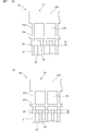
- the sound velocity of the first and second edge regions C1 and C2 is lowered by providing the wide portion, but as shown in FIG. 14, the first and second edge regions In C1 and C2, the mass addition films 25A and 26A may be laminated.
- the portion shown with hatching is the portion where the mass addition films 25A and 26A are laminated.
- the sound velocity of the first and second edge regions C1 and C2 can be lowered.
- an insulator such as silicon oxide or silicon nitride, or a metal or alloy such as Ni or W can be used.
- the mass addition films 25A and 26A may be provided in stripes along the elastic wave propagation direction so as to reach the region between the adjacent electrode fingers. In that case, it is necessary to use an insulating material as the material of the mass addition films 25A and 26A.
- the mass-added films 25A and 26A are provided in the elastic wave resonator 5 and the vertically coupled elastic wave resonator filter 6 to form the piston mode, the first and second edge regions C1 and 2 of the elastic wave resonator 5 are formed.
- the thicknesses of the mass-added films 25A and 26A in C2 may be the same as the thicknesses of the mass-added films 25A and 26A in the first and second edge regions C1 and C2 of the vertically coupled elastic wave resonator filter 6. ..
- the mass-added film may be laminated on the surface of the electrode finger opposite to the piezoelectric substrate side in the first and second edge regions, or may be laminated between the electrode finger and the piezoelectric substrate. ..
- the mass-added film passes from the first and second edge regions to the first and second gap regions, and is connected to the bus bar and the piezoelectric substrate. It may extend to the interval.
- the mass addition film may be replaced by a dielectric film formed so as to cover the IDT electrode and the piezoelectric substrate.
- the thickness of the dielectric film in the first and second edge regions is thicker than the thickness of the dielectric film in the central region. Also with this configuration, the speed of sound in the first and second edge regions can be made lower than that in the central region.
- high-speed films 27 and 28 for increasing the speed of sound may be laminated. ..
- the speed-up films 27 and 28 are not provided in the first and second edge regions C1 and C2.
- the high-speed film refers to a film in which the sound velocity of the bulk wave propagating in the high-speed film is faster than the sound velocity of the elastic wave propagating in the piezoelectric film, and the materials of the high-speed films 27 and 28 are Examples thereof include Al 2 O 3 , SiN, and Al N.
- the speed-up films 27 and 28 may be provided so as to extend in the elastic wave propagation direction. In this case, the speed-up films 27 and 28 may be integrated.
- the elastic wave resonator 5 and the vertically coupled elastic wave resonator filter 6 are provided with the speed-up films 27 and 28 to form the piston mode, the speed-up films 27 and 28 in the central region B of the elastic wave resonator 5 are formed.
- the thickness of the vertical coupling type elastic wave resonator filter 6 may be the same as the thickness of the speed-up films 27 and 28 in the central region B of the vertically coupled elastic wave resonator filter 6.
- the speed-up films 27 and 28 may be provided in the first and second edge regions C1 and C2.
- the film thickness of the speed-up films 27 and 28 in the first and second edge regions C1 and C2 is thinner than the film thickness of the speed-up films 27 and 28 in the central region B. Even with such a configuration, the sound velocity of the first and second edge regions C1 and C2 can be made lower than that of the central region B.
- the configuration in which the sound velocity of the first and second edge regions C1 and C2 is lower than the sound velocity of the central region B is not particularly limited.
- the hypersonic material layer may be a support substrate. That is, a support substrate made of a hypersonic material may be used.
- the length of the edge region in the vertically coupled elastic wave resonator filter is set.
- An example shorter than the length of the edge region in the elastic wave resonator is shown.
- the present invention is not limited to this example.
- the present invention includes at least one elastic wave resonator among the series arm resonators S1 to S3 and the parallel arm resonators P1 and P2 included in the transmission filter 3 shown in FIG. 1, and the vertical arm resonator included in the reception filter 2. It may be applied to the coupled elastic wave resonator filter 6.
- the length of the first and second edge regions C1 and C2 in the vertically coupled elastic wave resonator filter 6 is at least one of the series arm resonators S1 to S3 and the parallel arm resonators P1 and P2. It may be shorter than the length of the first and second edge regions C1 and C2 in the elastic wave resonator. That is, the present invention can be applied to any elastic wave device including one or more 1-port type elastic wave resonators and one or more vertically coupled elastic wave resonator filters, and the length of the edge region can be adjusted.
- the changing elastic wave resonator and the vertically coupled elastic wave resonator filter may be formed at any place in the elastic wave device.
- Inner bus bar part 24b ... Outer bus bar part 24c ... Opening 24d ... Connecting part 25, 26 ... Wide width part 25A , 26A ... Mass-added film 27, 28 ... High-speed film 31 ...
- Elastic wave device 32 ... Vertical coupling type elastic wave resonator filter 33 .
- Elastic wave resonator P1, P2 Parallel arm resonator S1 to S3 ... Series arm resonator
Landscapes
- Physics & Mathematics (AREA)
- Acoustics & Sound (AREA)
- Surface Acoustic Wave Elements And Circuit Networks Thereof (AREA)
Priority Applications (4)
| Application Number | Priority Date | Filing Date | Title |
|---|---|---|---|
| KR1020227002063A KR102636227B1 (ko) | 2019-08-30 | 2020-08-21 | 탄성파 장치 |
| JP2021542843A JP7268747B2 (ja) | 2019-08-30 | 2020-08-21 | 弾性波装置 |
| CN202080059195.0A CN114270707B (zh) | 2019-08-30 | 2020-08-21 | 弹性波装置 |
| US17/679,394 US12355425B2 (en) | 2019-08-30 | 2022-02-24 | Acoustic wave device |
Applications Claiming Priority (2)
| Application Number | Priority Date | Filing Date | Title |
|---|---|---|---|
| JP2019158337 | 2019-08-30 | ||
| JP2019-158337 | 2019-08-30 |
Related Child Applications (1)
| Application Number | Title | Priority Date | Filing Date |
|---|---|---|---|
| US17/679,394 Continuation US12355425B2 (en) | 2019-08-30 | 2022-02-24 | Acoustic wave device |
Publications (1)
| Publication Number | Publication Date |
|---|---|
| WO2021039639A1 true WO2021039639A1 (ja) | 2021-03-04 |
Family
ID=74683526
Family Applications (1)
| Application Number | Title | Priority Date | Filing Date |
|---|---|---|---|
| PCT/JP2020/031658 Ceased WO2021039639A1 (ja) | 2019-08-30 | 2020-08-21 | 弾性波装置 |
Country Status (5)
| Country | Link |
|---|---|
| US (1) | US12355425B2 (https=) |
| JP (1) | JP7268747B2 (https=) |
| KR (1) | KR102636227B1 (https=) |
| CN (1) | CN114270707B (https=) |
| WO (1) | WO2021039639A1 (https=) |
Cited By (4)
| Publication number | Priority date | Publication date | Assignee | Title |
|---|---|---|---|---|
| WO2022264933A1 (ja) * | 2021-06-16 | 2022-12-22 | 株式会社村田製作所 | 弾性波装置 |
| WO2023002858A1 (ja) * | 2021-07-21 | 2023-01-26 | 株式会社村田製作所 | 弾性波装置及びフィルタ装置 |
| WO2023048140A1 (ja) * | 2021-09-21 | 2023-03-30 | 株式会社村田製作所 | 弾性波装置 |
| WO2024043347A1 (ja) * | 2022-08-26 | 2024-02-29 | 株式会社村田製作所 | 弾性波装置及びフィルタ装置 |
Citations (4)
| Publication number | Priority date | Publication date | Assignee | Title |
|---|---|---|---|---|
| WO2015182522A1 (ja) * | 2014-05-26 | 2015-12-03 | 株式会社村田製作所 | 弾性波装置 |
| WO2016208446A1 (ja) * | 2015-06-24 | 2016-12-29 | 株式会社村田製作所 | フィルタ装置 |
| WO2018003338A1 (ja) * | 2016-06-27 | 2018-01-04 | 株式会社村田製作所 | 弾性波フィルタ装置 |
| WO2018225650A1 (ja) * | 2017-06-06 | 2018-12-13 | 株式会社村田製作所 | 弾性波フィルタ装置、マルチプレクサ及び複合フィルタ装置 |
Family Cites Families (8)
| Publication number | Priority date | Publication date | Assignee | Title |
|---|---|---|---|---|
| JPS553020Y2 (https=) | 1976-10-08 | 1980-01-24 | ||
| DE102010005596B4 (de) * | 2010-01-25 | 2015-11-05 | Epcos Ag | Elektroakustischer Wandler mit verringerten Verlusten durch transversale Emission und verbesserter Performance durch Unterdrückung transversaler Moden |
| EP3007358B1 (en) * | 2013-05-29 | 2019-10-23 | Murata Manufacturing Co., Ltd. | Elastic wave filter device |
| JP6513104B2 (ja) * | 2014-04-08 | 2019-05-15 | スカイワークスフィルターソリューションズジャパン株式会社 | 弾性波共振器、これを用いた弾性波フィルタ、アンテナ共用器、モジュール及び通信機器 |
| KR102083803B1 (ko) * | 2014-06-23 | 2020-03-03 | 가부시키가이샤 무라타 세이사쿠쇼 | 탄성파 장치 |
| DE112016001894B4 (de) * | 2015-04-24 | 2022-02-03 | Murata Manufacturing Co., Ltd. | Vorrichtung für elastische Wellen |
| JP6798562B2 (ja) * | 2016-10-28 | 2020-12-09 | 株式会社村田製作所 | ラダー型フィルタ、デュプレクサ及び弾性波フィルタ装置 |
| CN110140296B (zh) * | 2016-12-28 | 2023-01-13 | 株式会社村田制作所 | 纵耦合谐振器型弹性波滤波器 |
-
2020
- 2020-08-21 WO PCT/JP2020/031658 patent/WO2021039639A1/ja not_active Ceased
- 2020-08-21 CN CN202080059195.0A patent/CN114270707B/zh active Active
- 2020-08-21 JP JP2021542843A patent/JP7268747B2/ja active Active
- 2020-08-21 KR KR1020227002063A patent/KR102636227B1/ko active Active
-
2022
- 2022-02-24 US US17/679,394 patent/US12355425B2/en active Active
Patent Citations (4)
| Publication number | Priority date | Publication date | Assignee | Title |
|---|---|---|---|---|
| WO2015182522A1 (ja) * | 2014-05-26 | 2015-12-03 | 株式会社村田製作所 | 弾性波装置 |
| WO2016208446A1 (ja) * | 2015-06-24 | 2016-12-29 | 株式会社村田製作所 | フィルタ装置 |
| WO2018003338A1 (ja) * | 2016-06-27 | 2018-01-04 | 株式会社村田製作所 | 弾性波フィルタ装置 |
| WO2018225650A1 (ja) * | 2017-06-06 | 2018-12-13 | 株式会社村田製作所 | 弾性波フィルタ装置、マルチプレクサ及び複合フィルタ装置 |
Cited By (4)
| Publication number | Priority date | Publication date | Assignee | Title |
|---|---|---|---|---|
| WO2022264933A1 (ja) * | 2021-06-16 | 2022-12-22 | 株式会社村田製作所 | 弾性波装置 |
| WO2023002858A1 (ja) * | 2021-07-21 | 2023-01-26 | 株式会社村田製作所 | 弾性波装置及びフィルタ装置 |
| WO2023048140A1 (ja) * | 2021-09-21 | 2023-03-30 | 株式会社村田製作所 | 弾性波装置 |
| WO2024043347A1 (ja) * | 2022-08-26 | 2024-02-29 | 株式会社村田製作所 | 弾性波装置及びフィルタ装置 |
Also Published As
| Publication number | Publication date |
|---|---|
| CN114270707A (zh) | 2022-04-01 |
| US20220182037A1 (en) | 2022-06-09 |
| KR20220024799A (ko) | 2022-03-03 |
| KR102636227B1 (ko) | 2024-02-16 |
| CN114270707B (zh) | 2026-02-27 |
| US12355425B2 (en) | 2025-07-08 |
| JP7268747B2 (ja) | 2023-05-08 |
| JPWO2021039639A1 (https=) | 2021-03-04 |
Similar Documents
| Publication | Publication Date | Title |
|---|---|---|
| US12113509B2 (en) | Acoustic wave device with IDT electrode including al metal layer and high acoustic impedance metal layer | |
| CN107112975B (zh) | 弹性波装置 | |
| US9035725B2 (en) | Acoustic wave device | |
| WO2021187397A1 (ja) | 弾性波装置 | |
| WO2021039639A1 (ja) | 弾性波装置 | |
| WO2019177028A1 (ja) | 弾性波装置 | |
| KR20230146602A (ko) | 탄성파 장치 | |
| US12244296B2 (en) | Acoustic wave filter | |
| WO2020261763A1 (ja) | 弾性波装置 | |
| WO2021065684A1 (ja) | 弾性波装置 | |
| WO2021241364A1 (ja) | 弾性波装置 | |
| WO2020250572A1 (ja) | 弾性波装置 | |
| WO2021024762A1 (ja) | 弾性波フィルタ装置 | |
| WO2020262388A1 (ja) | フィルタ装置 | |
| CN115485973B (zh) | 弹性波装置 | |
| CN115777176B (zh) | 弹性波装置 | |
| WO2023048256A1 (ja) | 弾性波装置 | |
| JP7095745B2 (ja) | 弾性波装置、帯域通過型フィルタ、デュプレクサ及びマルチプレクサ | |
| WO2024262276A1 (ja) | 弾性波装置及びフィルタ装置 | |
| WO2022019169A1 (ja) | ラダー型フィルタ | |
| WO2024004862A1 (ja) | フィルタ装置および通信装置 | |
| WO2024143006A1 (ja) | 弾性波装置 | |
| WO2023080167A1 (ja) | フィルタ装置及びマルチプレクサ | |
| WO2022085565A1 (ja) | 弾性波装置 |
Legal Events
| Date | Code | Title | Description |
|---|---|---|---|
| 121 | Ep: the epo has been informed by wipo that ep was designated in this application |
Ref document number: 20857327 Country of ref document: EP Kind code of ref document: A1 |
|
| ENP | Entry into the national phase |
Ref document number: 2021542843 Country of ref document: JP Kind code of ref document: A |
|
| ENP | Entry into the national phase |
Ref document number: 20227002063 Country of ref document: KR Kind code of ref document: A |
|
| NENP | Non-entry into the national phase |
Ref country code: DE |
|
| 122 | Ep: pct application non-entry in european phase |
Ref document number: 20857327 Country of ref document: EP Kind code of ref document: A1 |