WO2021038363A1 - 半導体装置、電子機器 - Google Patents
半導体装置、電子機器 Download PDFInfo
- Publication number
- WO2021038363A1 WO2021038363A1 PCT/IB2020/057716 IB2020057716W WO2021038363A1 WO 2021038363 A1 WO2021038363 A1 WO 2021038363A1 IB 2020057716 W IB2020057716 W IB 2020057716W WO 2021038363 A1 WO2021038363 A1 WO 2021038363A1
- Authority
- WO
- WIPO (PCT)
- Prior art keywords
- wiring
- transistor
- region
- conductor
- semiconductor
- Prior art date
- Legal status (The legal status is an assumption and is not a legal conclusion. Google has not performed a legal analysis and makes no representation as to the accuracy of the status listed.)
- Ceased
Links
Images


Classifications
-
- H—ELECTRICITY
- H10—SEMICONDUCTOR DEVICES; ELECTRIC SOLID-STATE DEVICES NOT OTHERWISE PROVIDED FOR
- H10B—ELECTRONIC MEMORY DEVICES
- H10B12/00—Dynamic random access memory [DRAM] devices
-
- G—PHYSICS
- G11—INFORMATION STORAGE
- G11C—STATIC STORES
- G11C11/00—Digital stores characterised by the use of particular electric or magnetic storage elements; Storage elements therefor
- G11C11/21—Digital stores characterised by the use of particular electric or magnetic storage elements; Storage elements therefor using electric elements
- G11C11/34—Digital stores characterised by the use of particular electric or magnetic storage elements; Storage elements therefor using electric elements using semiconductor devices
- G11C11/40—Digital stores characterised by the use of particular electric or magnetic storage elements; Storage elements therefor using electric elements using semiconductor devices using transistors
- G11C11/401—Digital stores characterised by the use of particular electric or magnetic storage elements; Storage elements therefor using electric elements using semiconductor devices using transistors forming cells needing refreshing or charge regeneration, i.e. dynamic cells
- G11C11/403—Digital stores characterised by the use of particular electric or magnetic storage elements; Storage elements therefor using electric elements using semiconductor devices using transistors forming cells needing refreshing or charge regeneration, i.e. dynamic cells with charge regeneration common to a multiplicity of memory cells, i.e. external refresh
- G11C11/405—Digital stores characterised by the use of particular electric or magnetic storage elements; Storage elements therefor using electric elements using semiconductor devices using transistors forming cells needing refreshing or charge regeneration, i.e. dynamic cells with charge regeneration common to a multiplicity of memory cells, i.e. external refresh with three charge-transfer gates, e.g. MOS transistors, per cell
-
- G—PHYSICS
- G11—INFORMATION STORAGE
- G11C—STATIC STORES
- G11C11/00—Digital stores characterised by the use of particular electric or magnetic storage elements; Storage elements therefor
- G11C11/21—Digital stores characterised by the use of particular electric or magnetic storage elements; Storage elements therefor using electric elements
- G11C11/34—Digital stores characterised by the use of particular electric or magnetic storage elements; Storage elements therefor using electric elements using semiconductor devices
- G11C11/40—Digital stores characterised by the use of particular electric or magnetic storage elements; Storage elements therefor using electric elements using semiconductor devices using transistors
- G11C11/401—Digital stores characterised by the use of particular electric or magnetic storage elements; Storage elements therefor using electric elements using semiconductor devices using transistors forming cells needing refreshing or charge regeneration, i.e. dynamic cells
- G11C11/4063—Auxiliary circuits, e.g. for addressing, decoding, driving, writing, sensing or timing
- G11C11/407—Auxiliary circuits, e.g. for addressing, decoding, driving, writing, sensing or timing for memory cells of the field-effect type
- G11C11/409—Read-write [R-W] circuits
- G11C11/4097—Bit-line organisation, e.g. bit-line layout, folded bit lines
-
- G—PHYSICS
- G11—INFORMATION STORAGE
- G11C—STATIC STORES
- G11C8/00—Arrangements for selecting an address in a digital store
- G11C8/16—Multiple access memory array, e.g. addressing one storage element via at least two independent addressing line groups
-
- H—ELECTRICITY
- H10—SEMICONDUCTOR DEVICES; ELECTRIC SOLID-STATE DEVICES NOT OTHERWISE PROVIDED FOR
- H10B—ELECTRONIC MEMORY DEVICES
- H10B41/00—Electrically erasable-and-programmable ROM [EEPROM] devices comprising floating gates
- H10B41/70—Electrically erasable-and-programmable ROM [EEPROM] devices comprising floating gates the floating gate being an electrode shared by two or more components
-
- H—ELECTRICITY
- H10—SEMICONDUCTOR DEVICES; ELECTRIC SOLID-STATE DEVICES NOT OTHERWISE PROVIDED FOR
- H10D—INORGANIC ELECTRIC SEMICONDUCTOR DEVICES
- H10D86/00—Integrated devices formed in or on insulating or conducting substrates, e.g. formed in silicon-on-insulator [SOI] substrates or on stainless steel or glass substrates
- H10D86/40—Integrated devices formed in or on insulating or conducting substrates, e.g. formed in silicon-on-insulator [SOI] substrates or on stainless steel or glass substrates characterised by multiple TFTs
- H10D86/421—Integrated devices formed in or on insulating or conducting substrates, e.g. formed in silicon-on-insulator [SOI] substrates or on stainless steel or glass substrates characterised by multiple TFTs having a particular composition, shape or crystalline structure of the active layer
- H10D86/423—Integrated devices formed in or on insulating or conducting substrates, e.g. formed in silicon-on-insulator [SOI] substrates or on stainless steel or glass substrates characterised by multiple TFTs having a particular composition, shape or crystalline structure of the active layer comprising semiconductor materials not belonging to the Group IV, e.g. InGaZnO
-
- H—ELECTRICITY
- H10—SEMICONDUCTOR DEVICES; ELECTRIC SOLID-STATE DEVICES NOT OTHERWISE PROVIDED FOR
- H10D—INORGANIC ELECTRIC SEMICONDUCTOR DEVICES
- H10D86/00—Integrated devices formed in or on insulating or conducting substrates, e.g. formed in silicon-on-insulator [SOI] substrates or on stainless steel or glass substrates
- H10D86/40—Integrated devices formed in or on insulating or conducting substrates, e.g. formed in silicon-on-insulator [SOI] substrates or on stainless steel or glass substrates characterised by multiple TFTs
- H10D86/60—Integrated devices formed in or on insulating or conducting substrates, e.g. formed in silicon-on-insulator [SOI] substrates or on stainless steel or glass substrates characterised by multiple TFTs wherein the TFTs are in active matrices
Definitions
- One aspect of the present invention relates to a semiconductor device and an electronic device.
- one aspect of the present invention is not limited to the above technical fields.
- the technical field of one aspect of the invention disclosed in the present specification and the like relates to a product, a driving method, or a manufacturing method.
- the present invention relates to a process, machine, manufacture, or composition (composition of matter).
- one aspect of the present invention relates to a semiconductor device, a display device, a light emitting device, a power storage device, a storage device, a method for driving them, or a method for manufacturing them.
- the semiconductor device refers to an element, a circuit, a device, or the like that can function by utilizing the semiconductor characteristics.
- semiconductor elements such as transistors and diodes are semiconductor devices.
- the circuit having a semiconductor element is a semiconductor device.
- a device including a circuit having a semiconductor element is a semiconductor device.
- Mobile devices such as smartphones, tablets and electronic books, and electronic devices with semiconductor devices such as personal computers and servers are required to handle large amounts of data. Therefore, semiconductor devices are required to have a large storage capacity, low power consumption, and high processing time.
- Patent Document 1 discloses a semiconductor device in which memory cells are three-dimensionally stacked. Further, in order to realize a semiconductor device having a large storage capacity without changing the size of the chip of the semiconductor device, a technique for miniaturizing the circuit of the semiconductor device is required.
- a NAND flash memory known as a semiconductor device
- one aspect of the present invention is to provide a storage device having a new configuration.
- one aspect of the present invention is to provide a storage device with reduced power consumption.
- one aspect of the present invention is to provide a storage device in which the rewriting time is shortened.
- the present invention is a semiconductor device having a memory module.
- the memory module has a first memory cell, a first wire, a second wire, and a third wire.
- the second wiring and the third wiring contain metal oxides.
- the first memory cell has a first read transistor and a first rewrite transistor.
- the first wiring has a region that functions as a back gate of the first readout transistor and a region that functions the second wiring as a conductor.
- the second wiring has a region that functions as a channel forming region of the first readout transistor, a region that functions as a back gate of the first rewriting transistor, and a region that functions the third wiring as a conductor.
- the third wiring has a region that functions as a channel forming region of the first rewriting transistor and a region that functions as a conductor.
- the first rewrite transistor is formed in the same opening as the first read transistor, and the second wiring including the channel formation region of the first read transistor is the channel formation region of the first rewrite transistor. It is preferable that it is formed inside the third wiring including the above through an insulating layer.
- An electronic device having the above-mentioned semiconductor device and a housing is preferable.
- One aspect of the present invention can provide a storage device having a novel configuration. Alternatively, one aspect of the present invention can provide a storage device with reduced power consumption. Alternatively, one aspect of the present invention can provide a storage device in which the rewriting time is shortened.
- the effect of one aspect of the present invention is not limited to the effects listed above.
- the effects listed above do not preclude the existence of other effects.
- the other effects are the effects not mentioned in this item, which are described below. Effects not mentioned in this item can be derived from those described in the description or drawings by those skilled in the art, and can be appropriately extracted from these descriptions.
- one aspect of the present invention has at least one of the above-listed effects and / or other effects. Therefore, one aspect of the present invention may not have the effects listed above in some cases.
- FIG. 1A to 1C are circuit diagrams showing a configuration example of a semiconductor device.
- FIG. 2 is a circuit diagram showing a configuration example of a semiconductor device.
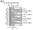
- FIG. 3 is an equivalent circuit diagram of a memory string.
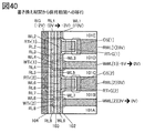
- FIG. 4 is an equivalent circuit diagram of a memory string.
- FIG. 5 is an equivalent circuit diagram of a memory string.
- FIG. 6 is an equivalent circuit diagram of a memory string.
- FIG. 7 is a timing chart showing an operation example of the semiconductor device.
- FIG. 8 is a timing chart showing an operation example of the semiconductor device.
- FIG. 9 is a timing chart showing an operation example of the semiconductor device.
- FIG. 10 is a circuit diagram showing a configuration example of a semiconductor device.
- FIG. 11 is a timing chart showing an operation example of the semiconductor device.
- FIG. 12 is a timing chart showing an operation example of the semiconductor device.
- 13A and 13B are block diagrams showing an example of a storage device.
- FIG. 14 is a circuit diagram showing a configuration example of a semiconductor device.
- FIG. 15 is a circuit diagram showing a configuration example of a semiconductor device.
- FIG. 16 is a circuit diagram showing a configuration example of a semiconductor device.
- 17A and 17B are a top view and a cross-sectional view for explaining a configuration example of the semiconductor device.
- 18A and 18B are cross-sectional views for explaining a manufacturing example of a semiconductor device.
- 19A and 19B are cross-sectional views for explaining a manufacturing example of a semiconductor device.
- 20A and 20B are cross-sectional views for explaining a manufacturing example of a semiconductor device.
- 21A and 21B are cross-sectional views for explaining a manufacturing example of a semiconductor device.
- 22A and 22B are cross-sectional views for explaining a manufacturing example of the semiconductor device.
- 23A and 23B are cross-sectional views for explaining a manufacturing example of the semiconductor device.
- 24A and 24B are cross-sectional views for explaining a manufacturing example of the semiconductor device.
- 25A and 25B are cross-sectional views for explaining a manufacturing example of the semiconductor device.
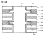
- 26A and 26B are cross-sectional views for explaining a manufacturing example of a semiconductor device.
- 27A and 27B are cross-sectional views for explaining a manufacturing example of the semiconductor device.
- FIG. 28 is a cross-sectional view for explaining a manufacturing example of the semiconductor device.
- FIG. 29 is a cross-sectional view for explaining a manufacturing example of the semiconductor device.
- FIG. 30 is a cross-sectional view for explaining a manufacturing example of the semiconductor device.
- FIG. 31 is a cross-sectional view for explaining the semiconductor device.
- 32A and 32B are cross-sectional views for explaining the semiconductor device.
- 33A and 33B are cross-sectional views for explaining a semiconductor device.
- FIG. 34 is a diagram illustrating a semiconductor device.
- FIG. 35 is a diagram illustrating an operation example of the semiconductor device.
- FIG. 36 is a diagram illustrating an operation example of the semiconductor device.
- FIG. 37 is a diagram illustrating an operation example of the semiconductor device.
- FIG. 38 is a diagram illustrating an operation example of the semiconductor device.
- FIG. 39 is a diagram illustrating an operation example of the semiconductor device.
- FIG. 40 is a diagram illustrating an operation example of the semiconductor device.
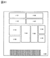
- FIG. 41 is a block diagram illustrating a CPU.
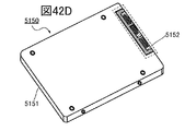
- 42A to 42E are perspective views showing an example of an electronic device.
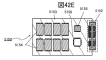
- 43A to 43F are perspective views showing an example of an electronic device.
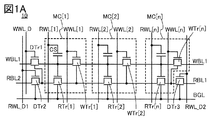
- the semiconductor device shown in FIG. 1A is a memory module 10 having n memory cells.
- the memory module 10 includes memory cell MC [1] to memory cell MC [n], selection transistor DTr1, selection transistor DTr2, selection transistor DTr3, wiring WWL_D, wiring RWL_D1, wiring RWL_D2, wiring WWL [1] to wiring WWL [n]. ], Wiring RWL [1] to Wiring RWL [n], Wiring WBL1, Wiring RBL1, and Wiring RBL2.
- the wiring WWL (wiring WWL [1] to wiring WWL [n]) functions as a rewrite word line
- the wiring RWL wiring RWL [1] to wiring RWL [n]) functions as a read word line
- the wiring WBL1 Functions as a rewrite bit line
- the wiring RBL1 and the wiring RBL2 function as a read bit line.
- n is an integer of 2 or more.
- Each of the memory cell MC [1] to the memory cell MC [n] has a transistor WTr and a transistor RTr.
- the transistor WTr (transistor WTr [1] to transistor WTr [n]) and the transistor RTr (transistor RTr [1] to transistor RTr [n]) shown in FIG. 1A are transistors having a small off-current. Is preferable. By using a transistor having a small off-current for the transistor WTr and the transistor RTr, the independence of the data held in the adjacent memory nodes can be ensured. Further, the transistor WTr and the transistor RTr are preferably transistors having a back gate. By applying a potential to the back gate, the threshold values of the transistor WTr and the transistor RTr can be controlled.
- FIG. 1A shows an example in which memory cells MC [1] to memory cells MC [n] are connected in series. It is preferable that the selection transistor DTr1 for rewriting the data stored in the memory cell is connected to either end of the memory cell MC [1] or the memory cell MC [n] connected in series. Further, a selection transistor DTr2 for reading data stored in the memory cell is connected to one end of one of the memory cells MC [1] and the memory cell MC [n] connected in series, and the other end is connected. Is preferably connected to a selection transistor DTr3 for reading data stored in a memory cell. FIG. 1A shows an example in which the selection transistor DTr1 and the selection transistor DTr2 are connected to the memory cell MC [1].
- Each memory cell has a capacitance CS and a memory node in addition to the transistor WTr and the transistor RTr.
- the transistor WTr functions as a rewrite transistor, and the transistor RTr functions as a read transistor.
- the memory node is formed by being electrically connected to one of the source or drain of the transistor WTr, the gate of the transistor RTr, and one of the electrodes of the capacitance CS.
- the gate of the transistor WTr is electrically connected to the wiring WWL
- the other electrode of the capacitive CS is electrically connected to the wiring RWL.
- the other of the source or drain of the transistor WTr [1] of the memory cell MC [1] is electrically connected to the memory node of the memory cell MC [2] connected in series with the memory cell MC [1]. ing.
- One of the source or drain of the selection transistor DTr1 is electrically connected to the wiring WBL1, and the other of the source or drain of the selection transistor DTr1 is electrically connected to the memory node of the memory cell MC [1].
- the gate of is electrically connected to the wiring WWL_D.
- the other of the source or drain of the transistor WTr [n] of the memory cell MC [n] is electrically connected to the wiring WBL1. That is, one end of a series of memory cells connected in series is electrically connected to the other end of the series of memory cells via the selection transistor DTr1 and the wiring WBL1.
- One of the source or drain of the selection transistor DTr2 is electrically connected to the wiring RBL2, and the other of the source or drain of the selection transistor DTr2 is connected to one of the source or drain of the transistor RTr [1] of the memory cell MC [1]. It is electrically connected and the gate of the selection transistor DTr2 is electrically connected to the wiring RWL_D1.
- the other of the source or drain of the transistor RTr [1] of the memory cell MC [1] is electrically connected to one of the source or drain of the transistor RTr [2] of the memory cell MC [2] connected in series. Has been done.
- the other of the source or drain of the transistor RTr [n] of the memory cell MC [n] is electrically connected to one of the source or drain of the selection transistor DTr3. Further, the other side of the source or drain of the selection transistor DTr3 is electrically connected to the wiring RBL1.
- the gate of the selection transistor DTr3 is electrically connected to the wiring RWL_D2. That is, the wiring RBL1 is electrically connected to the transistor RTr of the memory cells connected in series via the selection transistor DTr2, and the transistor RTr [n] of the memory cell MC [n] is connected via the selection transistor DTr2. Is electrically connected to the wiring RBL2.
- the back gate of the transistor WTr [1] included in the memory cell MC [1] is provided by the memory cell MC [2] with the other of the source or drain of the transistor RTr [1] included in the memory cell MC [1].
- One of the source and drain of the transistor RTr [2] is electrically connected to the connecting node.
- the back gate of the selection transistor DTr1 is electrically connected to a node to which the other of the source or drain of the selection transistor DTr2 and one of the source or drain of the transistor RTr [1] of the memory cell MC [1] are connected. Will be done.
- the wiring BGL shown in FIG. 1A is electrically connected to the back gate of the transistors RTr [1] to RTr [n] of the respective memory cells MC [1] to MC [n]. ing. Further, the selection transistor DTr2 and the selection transistor DTr3 preferably have a back gate like the transistor WTr [n], and as shown in FIG. 1A, the selection transistor DTr2 and the selection transistor DTr3 are respectively. The back gate is also preferably electrically connected to the wiring BGL.
- the transistor WTr connected in series and the memory node are connected. Can be rewritten via.
- the data is given from the wiring WBL1 via the selection transistor DTr1. It is preferable that the data is given from the wiring WBL1 connected to the memory cell MC [n] in order to rewrite the data of the memory cell MC [j] close to the memory cell MC [n].
- the data in the memory cell of any one of the memory cell MC [1] to the memory cell MC [n] is read out via the transistor RTr connected in series. be able to.
- the data read to the wiring RBL1 is given via the selection transistor DTr2, and it is close to the memory cell MC [n].
- the data read out to the wiring RBL2 is given via the selection transistor DTr3 connected to the memory cell MC [n].
- the channel forming portion of the selection transistor DTr1, the memory node, and the channel forming region of the transistor WTr are semiconductor layers containing the same metal oxide.
- the semiconductor layer containing the metal oxide can be made to function as a wiring by lowering the resistance value by adding an impurity containing hydrogen or the like.
- the semiconductor layer containing the metal oxide can be made to function as a wiring by lowering the resistance value by applying a positive electric field. Therefore, the semiconductor layer containing the metal oxide can be paraphrased as wiring.
- the channel forming portion of the selection transistor DTr2 and the selection transistor DTr3, the channel forming region of the readout transistor RTr, and the connection node between the transistors RTr are semiconductor layers containing a metal oxide. Therefore, the semiconductor layer containing the metal oxide can be paraphrased as wiring.
- the channel forming region of the transistor WTr and the transistor RTr has, for example, one or more metal oxides selected from indium, element M (element M is, for example, aluminum, gallium, yttrium, tin, etc.), and zinc. Is preferable.
- element M is, for example, aluminum, gallium, yttrium, tin, etc.
- zinc is, for example, aluminum, gallium, yttrium, tin, etc.
- the transistor in which the metal oxide is contained in the channel forming region has a characteristic that the off-current is very low.
- a transistor having a characteristic of low off-current to the transistor WTr that controls data retention, data can be retained in the memory cell MC for a long time. As a result, the number of times the retained data is refreshed can be reduced, so that the power consumption of the semiconductor device can be reduced.
- a transistor containing a metal oxide in the channel forming region can be called an OS transistor.
- the channel formation region of the transistor RTr it is preferable to use a material having a high field effect mobility of the transistor.
- the semiconductor device can be operated faster.
- indium, element M element M is, for example, aluminum, gallium, yttrium, tin, etc.
- metal oxide selected from zinc one or more. It can have a semiconductor material such as silicon.
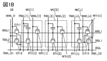
- a memory module 10 having a circuit configuration different from that of FIG. 1A will be described with reference to FIG. 1B.
- the wiring BGL shown in FIG. 1B shows an example in which the transistor WTr and the back gate of the transistor RTr of the respective memory cells MC [1] to MC [n] are electrically connected to each other. By applying a potential to the back gate, the threshold values of the transistor WTr and the transistor RTr can be controlled.
- the wiring BGL is electrically connected to the back gates of the transistors WTr and the transistors RTr included in the memory cells MC [1] to the memory cells MC [n] independently of each other. They may be connected to each other to supply different potentials.
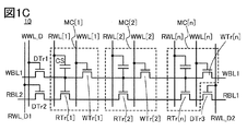
- the memory module 10 having a circuit configuration different from that of FIG. 1B will be described with reference to FIG. 1C.
- the transistor WTr or the transistor RTr is a transistor without a back gate.
- the transistor WTr can be formed in the same opening as the transistor RTr.
- the wiring including the channel forming region of the transistor RTr is preferably configured to be formed inside the wiring including the channel forming region of the transistor WTr via an insulating layer. It is preferable that a plurality of transistors WTr and transistors RTr are formed so as to alternately overlap each other in one opening. The structure will be described in detail with reference to FIGS. 14 to 29.
- the transistor WTr and the transistor RTr can be formed on a silicon substrate.
- the memory module 10 can be formed above the transistor formed on the silicon substrate. Therefore, in the case of providing a semiconductor device having a high information density per unit area, it is easy to realize by forming a plurality of transistors WTr and transistors RTr so as to be alternately overlapped in one opening.
- a plurality of transistors WTr and transistors RTr are formed in a plane.
- the manufacturing process can be simplified, and circuits having different functions can be mounted on the silicon substrate. Since a memory module including a transistor WTr and a transistor RTr can be formed on the circuit, it is suitable for mounting an embedded memory or the like. Further, by configuring the memory module on the circuit, the mounting space can be reduced.
- the memory modules 10 shown in FIG. 1A are arranged side by side in m columns, and the wiring RWL and the wiring WWL are electrically shared with the memory cell MC in the same row. It has a connected configuration. That is, the semiconductor device shown in FIG. 2 is a semiconductor device that can be represented in two dimensions of n rows and m columns, and has memory cells MC [1,1] to memory cells MC [m, n]. In FIG. 2, although not shown for the sake of simplicity, the semiconductor device is a three-dimensional memory cell MC [1,1,1] to a memory cell MC [m, n, d] by considering the depth direction. ] Can have. In the second embodiment, an example in which the semiconductor device has three-dimensional memory cells MC [1,1,1] to memory cells MC [m, n, d] will be described in detail. m, n, or d is an integer of 2 or more.
- the semiconductor device shown in FIG. 2 includes wiring WWL_D, wiring RWL_D1, wiring RWL_D2, wiring RWL [1] to wiring RWL [n], wiring WWL [1] to wiring WWL [n], wiring RBL1 [1] to wiring RBL1 [ m], wiring RBL2 [1] to wiring RBL2 [m], wiring WBL1 [1] to wiring WBL1 [m], and wiring BGL [1] to wiring BGL [m].
- the other electrode of the capacitance CS of the memory cell MC [i, j] (not shown) is electrically connected to the wiring RWL [j], and the transistor WTr of the memory cell MC [i, j] is connected.
- the gate of [i, j] is electrically connected to the wiring WWL [j].
- one of the source or drain of the selection transistor DTr1 [i] and the other of the source or drain of the transistor WTr [i, n] of the memory cell MC [i, n] are electrically connected.
- the wiring RBL1 [i] is electrically connected to the source or drain of the transistor RTr [i, n] of the memory cell MC [i, n].
- the wiring RBL2 [i] is electrically connected to one of the source and drain of the transistor RTr of the memory cell MC [i, 1].
- i is an integer of 1 or more and m or less, and j is an integer of 1 or more and n or less.
- the transistor WTr, the transistor RTr, and the capacitive element CS included in the memory cell MC [1] are shown as the transistor WTr [1], the transistor RTr [1], and the capacitive element CS [1], respectively. ..
- the transistor WTr, the transistor RTr, and the capacitive element CS included in the memory cells MC [2] to the memory cells MC [4] are also shown.
- the number of memory cell MCs included in the memory module 10 is not limited to 4. Assuming that the number of memory cell MCs included in the memory module 10 is n, n may be an integer of 2 or more.
- a configuration in which a plurality of memory cell MCs are connected in series means the drain (or source) of the transistor WTr [k] included in the memory cell MC [k] (k is an integer of 1 or more and n-1 or less). ) Is electrically connected to the source (or drain) of the transistor WTr [k + 1] included in the memory cell MC [k + 1], and the drain (or source) of the transistor RTr [k] included in the memory cell MC [k]. Refers to a configuration in which is electrically connected to the source (or drain) of the transistor RTr [k + 1] included in the memory cell MC [k + 1].
- a single crystal semiconductor, a polycrystalline semiconductor, a microcrystal semiconductor, an amorphous semiconductor, or the like can be used alone or in combination.
- the semiconductor material for example, silicon, germanium, or the like can be used.
- compound semiconductors such as silicon germanium, silicon carbide, gallium arsenide, oxide semiconductors, and nitride semiconductors may be used.
- the semiconductor used for the transistor may be a laminate of semiconductors.
- semiconductors having different crystal states may be used, or different semiconductor materials may be used.
- the transistor WTr is preferably an OS transistor in which an oxide semiconductor, which is a kind of metal oxide, is used in the semiconductor layer on which a channel is formed. Since the oxide semiconductor has a band gap of 2 eV or more, the off-current is remarkably small.
- an OS transistor is used as the transistor WTr, the electric charge written in the node ND (also referred to as “storage node”) can be retained for a long period of time.
- the memory cell MC can be called an “OS memory”. Further, the memory module 10 including the memory cell MC can also be called an "OS memory”.
- a NAND type storage device including an OS memory is also referred to as an "OS NAND type” or an “OS NAND type storage device”. Further, an OS NAND type storage device having a configuration in which a plurality of OS memories are stacked in the Z direction is also referred to as a "3D OS NAND type” or a “3D OS NAND type storage device”.
- the transistor RTr may be a transistor (also referred to as "Si transistor") in which silicon is used in the semiconductor layer on which the channel is formed.
- the transistor RTr may be formed of a Si transistor, and the transistor WTr may be formed of an OS transistor.
- FIG. 4 shows an equivalent circuit diagram of the memory module 10 when an OS transistor is used as the transistor WTr and a Si transistor is used as the transistor RTr.
- the OS memory can retain the information written for a period of one year or more, or even ten years or more, even if the power supply is stopped. Therefore, the OS memory can be regarded as a non-volatile memory.
- the OS memory can hold not only binary (1 bit) but also multi-value (multi-bit) information.
- the OS memory is a method of writing an electric charge to a node via an OS transistor, the high voltage required for a conventional flash memory is not required, and a high-speed writing operation can be realized. Further, the erasing operation before data rewriting performed in the flash memory is unnecessary in the OS memory. Also, since no charge is injected or withdrawn into the floating gate or charge capture layer, the OS memory is capable of writing and reading data virtually unlimited times. The OS memory has less deterioration than the conventional flash memory, and high reliability can be obtained.
- OS memory does not involve structural changes at the atomic level. Therefore, the OS memory is superior in rewrite resistance to the magnetic resistance memory and the resistance change type memory.
- the off-current of the OS transistor hardly increases even in a high temperature environment. Specifically, the off-current hardly increases even at an environmental temperature of room temperature or higher and 200 ° C. or lower. In addition, the on-current does not easily decrease even in a high temperature environment.
- the storage device including the OS memory has stable operation even in a high temperature environment, and high reliability can be obtained. Further, the OS transistor has a high dielectric strength between the source and the drain. By using an OS transistor as the transistor constituting the semiconductor device, the operation is stable even in a high temperature environment, and a semiconductor device with good reliability can be realized.
- a Si transistor may be used as the transistor WTr and an OS transistor may be used as the transistor RTr depending on the purpose or application. Further, as shown in FIG. 6, Si transistors may be used for both the transistor WTr and the transistor RTr depending on the purpose or application.
- the storage capacity per unit area can be increased.
- the structure of the data stored in the memory module of the semiconductor device shown in FIG. 2 is preferably represented by bits having a data width as the minimum unit.
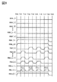
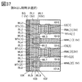
- the operation of rewriting the data of the first line, the second line, the n-1 line, and the nth line will be described with reference to the timing chart of FIG.
- the selection transistor DTr1 [1] to the selection transistor DTr1 [m] are turned on by giving "H” to the wiring WWL_D. Further, when “H” is given to the wiring WWL [1], the respective transistors WTr of the memory cells MC [1,1] to MC [m, 1] are turned on.
- the wirings WBL1 [1] to WBL1 [m] transmit data D [2] to memory cells MC [1, 2] to memory cells MC [m, via the selection transistor DTr1 [1] to the selection transistor DTr1 [m]. It can be given to each memory node of 2].
- data D [2] is also given to each memory node of the memory cell MC [1,1] to the memory cell MC [m, 1].
- the data D is preferably digital data having a data width of m bits.
- the data D may be given analog data.
- the analog data is preferably controlled by the potential. The amount of data that can be stored in a semiconductor device can be dramatically improved by handling analog data in which each bit is different.
- the respective transistors WTr of the memory cells MC [1,1] to MC [m, 1] are turned off. Therefore, the data D [2] is held in each memory node of the memory cells MC [1, 2] to the memory cells MC [m, 2]. Further, the data D [1] given to the wiring WBL1 [1] to the wiring WBL1 [m] is the memory cell MC [1,1] to the memory cell via the selection transistor DTr1 [1] to the selection transistor DTr1 [m]. The data of each memory node of MC [m, 1] can be rewritten.
- the selection transistor DTr1 [1] to the selection transistor DTr1 [m] are turned off by giving "L" to the wiring WWL_D. Therefore, the data D [1] is held in each of the memory nodes of the memory cells MC [1,1] to the memory cells MC [m, 1].
- the wiring WWL [n-1] is given an “H” so that the respective transistors WTr of the memory cells MC [1, n-1] to the memory cells MC [m, n-1] are assigned. Turns on. Further, when “H” is given to the wiring WWL [n], the respective transistors WTr of the memory cells MC [1, n] to the memory cells MC [m, n] are turned on.
- the data D [n-1] given to the wiring WBL1 [1] to the wiring WBL1 [m] is stored in the memory via the respective memory nodes of the memory cells MC [1, n] to the memory cells MC [m, n]. The data of each memory node of the cell MC [1, n-1] to the memory cell MC [m, n-1] can be rewritten.
- the respective transistors WTr of the memory cells MC [1, n-1] to the memory cells MC [m, n-1] are turned off. become. Therefore, the data D [n-1] is held in each of the memory nodes of the memory cells MC [1, n-1] to the memory cells MC [m, n-1]. Further, the wiring WBL1 [1] to the wiring WBL1 [m] can provide the data D [n] to the respective memory nodes of the memory cells MC [1, n] to the memory cells MC [m, n].
- NAND flash memory it is necessary to update the data in all rows of the memory module in order to update the memory cell of any one of the memory modules in which the memory cells are connected in series.
- the data can be rewritten from an arbitrary line of the memory module, the data can be rewritten at high speed.
- FIG. 8 describes rewriting the data in the third line.
- the data D [3] is held in the memory cells MC [1,3] to the memory cells MC [m, 3] as the data in the third row during the period from the time T21 to the time T22.
- any row to be rewritten can be accessed from the memory cell MC in the first row to which the selection transistor DTr1 is connected or the memory cell MC in the nth row, whichever is closer. preferable.
- the rewrite time of the memory cell corresponds to the number of rows up to an arbitrary rewrite target row. Therefore, the rewriting time can be shortened by accessing the line to be rewritten from a side close to the desired line.
- the semiconductor device is a storage device having an m-bit data width (mbit / width) for an arbitrary address.
- the wiring RBL1 [1] to the wiring RBL1 [m] can be initialized at an arbitrary potential. Further, the wiring RBL2 [1] to the wiring RBL2 [m] are provided with a reference potential for confirming that arbitrary data is stored in the memory cell. Any potential to be initialized is preferably the same potential as the "L" of the data or lower than the "L” of the data. During the period when the reference potential is given to the wiring RBL2 [1] to the wiring RBL2 [m], "H" is given to the wiring RWL_D1 and the wiring RWL_D2, and the selection transistor DTr2 and the selection transistor DTr3 are turned on.
- the respective data stored in the memory cells MC [1,1] to the memory cells MC [m, 1] connected to the wiring RWL [1] can be read out.
- “L” is given to the wiring RWL [1]
- “H” is given to the other wiring RWL [2] to the wiring RWL [n]. Since the transistors RTr are connected in series, if the data of "H” is held in any of the memory cells MC [1,1] to the memory cells MC [m, 1], the data of "H” A reference potential signal is output to the wiring RBL1 in the target row of the memory cell MC in which the is held.
- Each memory cell MC connected to the wiring RWL [2] to the wiring RWL [n] is given an “H” to the wiring RWL [2] to the wiring RWL [n], so that the capacitance CS is a transistor according to the charge conservation law.
- the gate of the RTr can be in a state where "H” is given. Therefore, in the transistors RTr connected in series, all the transistors RTr other than the reading target are turned on. Therefore, when the data of the memory cell to be read is “L”, the reference potential given to the wiring RBL2 cannot be output to the wiring RBL1. Further, when the data of the memory cell to be read is “H”, the reference potential given to the wiring RBL2 is output to the wiring RBL1. Therefore, each data stored in the memory cell MC [1,1] to the memory cell MC [m, 1] is output to the wiring RBL1 [1] to the wiring RBL1 [m].
- the data held in the memory cells MC [1, 2] to the memory cells MC [m, 2] connected to the wiring RWL [2] can be read out.
- “L” is given to the wiring RWL [2]
- “H” is given to the other wiring RWL [1] and the wiring RWL [3] to the wiring RWL [n].
- the description will be omitted because the operation is the same as the operation of reading data from the wiring RWL [1].
- time T34 is the same as the operation at the time T32, the description thereof will be omitted.
- the time T34 (the period from the time T35 to the time T39), it is connected to the wiring RWL [3] to the wiring RWL [n] by performing the read operation line by line in the same manner as the operation of the time T31 and the time T33.
- the data stored in the memory cell MC can be read out. Therefore, the data read from the memory cell MC can be sequentially read in the row direction of the memory cell.
- FIG. 10 A semiconductor device different from FIG. 2 will be described with reference to FIG.
- the semiconductor device shown in FIG. 10 differs from FIG. 2 in that one of the source and drain of the selection transistor DTr1 is electrically connected to the wiring WBL2.
- the memory module 10 will be used as an example.
- the memory module 10 Since the wiring WBL2 is electrically connected to one of the source and drain of the selection transistor DTr1, the memory module 10 rewrites data to the memory cell MC from either one or both of the wiring WBL1 and the wiring WBL2. Can be done.
- the wiring WBL2 [1] can rewrite the data of the memory node of the memory cell MC [1,1] via the selection transistor DTr1 [1]. Further, by giving "H” to the wiring WWL [n], the wiring WBL1 [1] can rewrite the data of the memory node of the memory cell MC [1, n]. Further, by simultaneously giving “H” to the wiring WWL [1] and the wiring WWL [n], the data of the memory nodes of the memory cells MC [1,1] and the memory cells MC [1, n] can be rewritten at the same time. Can be done.
- wiring WWL_D wiring WWL [1] to wiring WWL [n]
- wiring RWL_D1 wiring RWL_D2
- wiring RWL [1] to wiring RWL [n] wiring RBL1 [1]
- wiring RBL2 [2] "L” is given. Further, no data is input to the wiring WBL1 [1] and the wiring WBL2 [1].
- the selection transistor DTr1 [1] to the selection transistor DTr1 [m] are turned on by giving "H" to the wiring WWL_D. Further, when “H” is given to the wiring WWL [1], the respective transistors WTr of the memory cells MC [1,1] to the memory cells MC [m, 1] are turned on. Therefore, the data D [2] given to the wiring WBL2 [1] to the wiring WBL2 [m] is the respective memory cells MC [1, 2] via the selection transistor DTr1 [1] to the selection transistor DTr1 [m]. The data in the memory cell MC [m, 2] can be rewritten. At this time, the data D [2] is also given to the memory cells MC [1,1] to the memory cells MC [m, 1].
- each transistor WTr of the memory cells MC [1, n] to the memory cells MC [m, n] is turned on.
- the respective transistors WTr of the memory cells MC [1, n-1] to the memory cells MC [m, n-1] are turned on.
- the data D [n-1] given to the wiring WBL1 [1] to the wiring WBL1 [m] is the memory cell MC [1, n-1] to the memory cell MC [m, n-1], respectively.
- the data in the memory node can be rewritten.
- data D [n-1] is also given to the memory cells MC [1, n] to the memory cells MC [m, n].
- the data D [1] given to the wiring WBL2 [1] to the wiring WBL2 [m] is the memory cell MC [1,1] to the memory via the selection transistor DTr1 [1] to the selection transistor DTr1 [m].
- Each data in the cell MC [m, 1] can be rewritten.
- the data D [n] given to the wiring WBL2 [1] to the wiring WBL2 [m] is the memory cells MC [1, n] to the memory via the selection transistor DTr1 [1] to the selection transistor DTr1 [m].
- the data in the cells MC [m, n] can be rewritten.
- FIG. 12 a plurality of memory modules included in the semiconductor device are connected by wiring WWL, wiring RWL, and wiring WWL_D, and an example in which the stored data structure has a data width of m bits will be described.
- the operation of rewriting the data of the first line, the second line, the third line, the n-1 line, and the nth line will be described with reference to the timing chart of FIG.
- the memory cell MC in the first row to which the selection transistor DTr1 is connected or the memory cell MC in the nth row, whichever is closer, is used. It is preferable to access the rows at the same time. Since two different rows can be rewritten at the same time, the rewriting time to the memory cell can be further shortened. Therefore, the rewriting time can be shortened by accessing the line to be rewritten from a side close to the desired line.
- the semiconductor device is a storage device having a data width of m bits for an arbitrary address.
- FIG. 13A shows an example of the configuration of the storage device.
- the storage device 2600 has a peripheral circuit 2601 and a memory cell array 2610.
- the peripheral circuit 2601 has a low decoder 2621, a word line driver circuit 2622, a bit line driver circuit 2630, an output circuit 2640, and a control logic circuit 2660.
- the semiconductor device shown in FIGS. 1A, 1B, or 1C described in the first embodiment can be applied to the memory cell array 2610.
- the bit line driver circuit 2630 includes a column decoder 2631, a precharge circuit 2632, a sense amplifier 2633, and a write circuit 2634.
- the precharge circuit 2632 has a function of precharging the wiring RBL2 described in the first embodiment to a predetermined potential.
- the sense amplifier 2633 has a function of acquiring the potential output from the memory cell MC to the wiring RBL1 as a data signal and amplifying the data signal. The amplified data signal is output to the outside of the storage device 2600 as a digital data signal RDATA via the output circuit 2640.
- the storage device 2600 is supplied with a low power supply potential (VSS), a high power supply potential (VDD) for the peripheral circuit 2601, and a high power supply potential (VIL) for the memory cell array 2610 as power supply potentials from the outside.
- VSS low power supply potential
- VDD high power supply potential
- VIL high power supply potential
- control signal (CE, WE, RE), the address signal ADDR, and the data signal WDATA are input to the storage device 2600 from the outside.
- the address signal ADDR is input to the low decoder 2621 and the column decoder 2631, and the data signal WDATA is input to the write circuit 2634.
- the control logic circuit 2660 processes input signals (CE, WE, RE) from the outside to generate control signals for the low decoder 2621 and the column decoder 2631.
- CE is a chip enable signal
- WE is a write enable signal
- RE is a read enable signal.
- the signal processed by the control logic circuit 2660 is not limited to this, and other control signals may be input as needed.
- FIG. 13B shows an example in which the storage device 2600 is configured by using a p-channel type Si transistor and a transistor containing an oxide semiconductor (preferably an oxide containing In, Ga, and Zn) in the channel forming region.
- the storage device 2600 shown in FIG. 13B has a logic layer 1000 and a memory layer 2000 whose peripheral circuits are composed of Si transistors. That is, the memory layer 2000 formed by the transistors including the oxide semiconductor in the channel forming region is formed above the logic layer 1000.
- the wiring length of the wiring RBL1 connecting the sense amplifier 2633 and the memory cell MC can be shortened. Therefore, the wiring RBL1 can reduce the influence of the time constant of the wiring and improve the reading operation speed of the data from the memory cell MC. Further, by using a transistor having an oxide semiconductor in the memory cell MC, the off current of the memory cell MC can be reduced. Since data leakage between adjacent memory cell MCs can be suppressed, data can be stored for a long period of time. Further, since the refresh interval of the memory cells can be lengthened, the power consumption of the storage device 2600 can be reduced. Further, by using only the p-channel type Si transistor, the manufacturing cost can be kept low. Alternatively, the Si transistor may be only an n-channel type.
- FIGS. 14 to 16 show the configuration of the memory cell array 2610 of FIG. In FIGS. 14 to 16, some elements are omitted for the sake of clarity of the figure.
- the memory cell MC [m, n, d] is connected to the wiring RBL1 [m], the wiring WBL1 [m], the wiring WWL [n, d], and the wiring RWL [n, d]. Therefore, the semiconductor device shown in FIG. 14 has memory cells MC [1,1,1] to memory cells MC [m, n, d] arranged three-dimensionally having a depth direction.
- FIG. 14 has a selection transistor DTr1, a selection transistor DTr2, a selection transistor DTr3, a wiring WWL_D, a wiring RWL_D1, and a wiring RWL_D2.
- the wiring WBL1 is connected to one end and the other end of the memory module 10 via the selection transistor DTr1
- the wiring RBL2 is connected to one end of the memory module 10 via the selection transistor DTr2
- the wiring RBL1 is connected to the selection transistor DTr3. Is connected to the other end of the memory module 10 via.
- the wiring WWL_D is electrically connected to the gate of the selection transistor DTr1
- the wiring RWL_D1 is electrically connected to the gate of the selection transistor DTr2
- the wiring RWL_D2 is electrically connected to the gate of the selection transistor DTr3.
- the selection transistor DTr2 can be precharged to each memory module 10 at a predetermined potential used for reading data.
- the wiring RBL2 may be fixed at an arbitrary high potential. Further, the selection transistor DTr3 can select the memory module 10 for reading data.
- the wiring RWL_D2 for reading data can individually turn off the selection transistor DTr3 connected to the unselected memory module 10.
- the non-selected memory module 10 can be separated, the signal quality of the data read from the selected memory cell to the wiring RBL1 can be improved.
- the selection transistor DTr3 when reading data from the wiring RBL2, the selection transistor DTr2 can be controlled.
- the selection transistor DTr2 or the selection transistor DTr3 can be provided as needed.
- the wiring RBL1 and the wiring WBL1 are connected to the bit line driver circuit 2630A in column units and in the depth direction d.
- the wiring RBL2 is electrically connected to the bit line driver circuit 2630B in column units and in the depth direction d. Therefore, the memory cells MC [1,1] to the memory cells MC [m, n] are processed as data access units. That is, it indicates that the data width has m bits.
- the semiconductor device of this embodiment can be easily applied not only to a general-purpose memory but also to a frame memory of a display device.
- each memory module 10 can reduce the variation due to the wiring resistance by shortening the wiring length of the wiring WBL1, so that the data rewriting time can be shortened.
- FIG. 15 shows a configuration of a memory cell array 2610 different from that of FIG.
- the wiring WBL1a is further provided, and the wiring WBL1a is electrically connected to the memory module 10 via the selection transistor DTr1.
- the wiring WBL1 is electrically connected in the vicinity of the memory module 10, and the memory module 10 shares the wiring WBL1 and is electrically connected to the bit line driver circuit 2630A.
- FIG. 15 shows an example in which the memory module 10 is electrically connected to the bit line driver circuit 2630A via the wiring WBL1 and is electrically connected to the bit line driver circuit 2630B via the wiring WBL1a. It is preferable that the wiring WBL1 or the wiring WBL1a shown in FIG.
- bit line driver circuit 2630A and the bit line driver circuit 2630B are electrically connected to the bit line driver circuit 2630A and the bit line driver circuit 2630B outside the memory cell array 2610.
- the bit line driver circuit 2630A and the bit line driver circuit 2630B preferably function as one bit line driver circuit 2630. Therefore, in the memory cell array 2610 shown in FIG. 15, it is not necessary to connect the wiring WBL1 in the vicinity of the memory module 10, so that the data density of the semiconductor device can be improved.
- FIG. 15 shows a configuration of a memory cell array 2610 different from that of FIG.
- the wiring WBL1a is further provided, and the wiring WBL1a is electrically connected to the memory module 10 via the selection transistor DTr1.
- the wiring WBL1 is connected in the vicinity of the memory module 10, and the memory module 10 shares the wiring WBL1 and is connected to the bit line driver circuit 2630A.
- FIG. 15 shows an example in which the memory module 10 is connected to the bit line driver circuit 2630A via the wiring WBL1 or the wiring WBL2.
- the wiring WBL1 or wiring WBL2 shown in FIG. 15 is preferably connected to the bit line driver circuit 2630A outside the memory cell array 2610. Therefore, the memory cell array 2610 can improve the data density of the semiconductor device as compared with the configuration shown in FIG.
- one of the memory modules 10 is connected to the wiring WBL2 via the selection transistor DTr1.
- the wiring WBL1 and the wiring RBL1 are connected to the bit line driver circuit 2630A, and the wiring WBL2 and the wiring RBL2 are connected to the bit line driver circuit 2630B. Therefore, the memory module 10 can rewrite the data by the signal given to the wiring WBL1 from the bit line driver circuit 2630A and the signal given to the wiring WBL2 from the bit line driver circuit 2630B. Further, as described with reference to FIG. 12, the same memory module 10 can be rewritten or read at the same time from the bit line driver circuit 2630A and the bit line driver circuit 2630B.
- FIGS. 1A to 1C are schematic views showing the semiconductor devices shown in FIGS. 1A to 1C.
- FIG. 17A shows a top view of the semiconductor device
- FIG. 17B shows a cross-sectional view corresponding to the alternate long and short dash line A1-A2 of FIG. 17A.
- the semiconductor device has a structure in which a wiring RWL, a wiring WWL, and an insulator (a region in which hatching is not shown in FIGS. 17A and 17B) are laminated, and an opening is provided in the structure.
- the conductor PG is formed so as to fill the opening.
- a wiring ER is formed on the conductor PG, whereby the wiring ER and the wiring WWL_D, the wiring RWL_D1, the wiring RWL_D2, the wiring RWL, or the wiring WWL are electrically connected.
- an opening is formed in the structure so as to penetrate the wiring RWL and the wiring WWL at once.
- the selection transistor DTr1 and the selection transistor DTr2 are in the region DM1 through which the wiring WWL_D, the wiring RWL, and the wiring WWL are penetrated
- the transistor WTr and the transistor RTr of the memory cell MC are in the region AR
- the selection transistor is in the region DM2.
- DTr3 can be provided. Therefore, an insulator, a conductor, and a semiconductor for forming the transistor are formed in the opening.
- the conductor functions as a wiring WBL and a wiring RBL
- the semiconductor functions as a channel forming region of the selection transistor DTr1, the selection transistor DTr2, the selection transistor DTr3, the transistor WTr, and the transistor RTr.
- a region in which an insulator, a conductor, and a semiconductor are formed in the opening is illustrated as a region HL.
- the transistor is provided with a back gate, the conductor possessed by the region HL functions as the back gate. Therefore, the back gate can be rephrased as wiring BGL.
- FIG. 17 shows that the semiconductor device shown in either FIG. 1A or FIG. 1B is configured in the region SD1, and the semiconductor device shown in FIG. 2 or FIG. 10 is configured in the region SD2. ..
- the following manufacturing method example 1 and manufacturing method example 2 describe a method for forming a transistor included in the memory cell MC formed in the region AR.
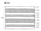
- 18 to 22 are cross-sectional views for explaining a manufacturing example of the semiconductor device shown in FIG. 1A, and in particular, show a cross-sectional view of a transistor WTr and a transistor RTr in the channel length direction. Further, in the cross-sectional views of FIGS. 18 to 22, some elements are omitted for the purpose of clarifying the figure.
- the semiconductor device of FIG. 1A is arranged on an insulator 101A arranged above a substrate (not shown), a conductor 131A arranged on the insulator 101A, and a conductor 131A.
- the laminate 100 having the plurality of conductors and the plurality of insulators will be referred to as the laminate 100.
- an insulator substrate, a semiconductor substrate, or a conductor substrate may be used as the substrate.
- the insulator substrate include a glass substrate, a quartz substrate, a sapphire substrate, a stabilized zirconia substrate (yttria-stabilized zirconia substrate, etc.), a resin substrate, and the like.
- the semiconductor substrate include a semiconductor substrate made of silicon, germanium, etc., or a compound semiconductor substrate made of silicon carbide, silicon germanium, gallium arsenide, indium phosphide, zinc oxide, gallium oxide, and the like.
- the conductor substrate includes a graphite substrate, a metal substrate, an alloy substrate, and a conductive resin substrate.
- a substrate having a metal nitride a substrate having a metal oxide, and the like.
- a substrate in which a conductor or a semiconductor is provided in an insulator substrate a substrate in which a conductor or an insulator is provided in a semiconductor substrate, a substrate in which a semiconductor or an insulator is provided in a conductor substrate, and the like.
- those on which an element is provided may be used.
- Elements provided on the substrate include a capacitance, a resistance element, a transistor, a switch element, a light emitting element, a storage element, and the like.
- a flexible substrate may be used as the substrate.
- a method of providing a transistor on a flexible substrate there is also a method of forming a transistor on a non-flexible substrate, peeling off the transistor, and transposing the transistor on the flexible substrate.
- a release layer may be provided between the non-flexible substrate and the transistor.
- the substrate a sheet, film, foil or the like in which fibers are woven may be used.
- the substrate may have elasticity. Further, the substrate may have a property of returning to the original shape when the bending or pulling is stopped. Alternatively, it may have a property of not returning to the original shape.
- the substrate has, for example, a region having a thickness of 5 ⁇ m or more and 700 ⁇ m or less, preferably 10 ⁇ m or more and 500 ⁇ m or less, and more preferably 15 ⁇ m or more and 300 ⁇ m or less.
- the substrate By making the substrate thinner, the weight of the semiconductor device having a transistor can be reduced. Further, by making the substrate thinner, it may have elasticity even when glass or the like is used, or it may have a property of returning to the original shape when bending or pulling is stopped. Therefore, it is possible to alleviate the impact applied to the semiconductor device on the substrate due to dropping or the like. That is, it is possible to provide a durable semiconductor device.
- the flexible substrate for example, metal, alloy, resin or glass, fibers thereof, or the like can be used.
- a material having a linear expansion coefficient of 1 ⁇ 10 -3 / K or less, 5 ⁇ 10 -5 / K or less, or 1 ⁇ 10 -5 / K or less may be used.
- the resin include polyester, polyolefin, polyamide (nylon, aramid, etc.), polyimide, polycarbonate, acrylic and the like.
- aramid has a low coefficient of linear expansion and is therefore suitable as a flexible substrate.
- the conductor 131A (conductor 131B) functions as the wiring WWL shown in FIG. 1A
- the conductor 132A (conductor 132B) functions as the wiring RWL shown in FIG. 1A.
- Examples of the conductor 131A, the conductor 131B, the conductor 132A, and the conductor 132B include aluminum, chromium, copper, silver, gold, platinum, tantalum, nickel, titanium, molybdenum, tungsten, hafnium, vanadium, niobium, manganese, and the like.
- a material containing at least one metal element selected from magnesium, zirconium, beryllium, indium, ruthenium and the like can be used.
- a semiconductor having high electrical conductivity typified by polycrystalline silicon containing an impurity element such as phosphorus, and SiO such as nickel silicide may be used.
- a conductive material containing a metal element and oxygen contained in a metal oxide applicable to the semiconductor 1, semiconductor 152, semiconductor 153a, and semiconductor 153b described later is used. You may use it.
- the above-mentioned conductive material containing a metal element and nitrogen may be used.
- a conductive material containing nitrogen such as titanium nitride and tantalum nitride may be used.
- indium tin oxide indium tin oxide, indium oxide containing tungsten oxide, indium zinc oxide containing tungsten oxide, indium oxide containing titanium oxide, indium tin oxide containing titanium oxide, indium zinc oxide, and silicon were added.
- Indium tin oxide may be used.
- indium gallium zinc oxide containing nitrogen may be used. By using such a material, it may be possible to capture hydrogen mixed in from a surrounding insulator or the like.
- a conductive material having a function of suppressing the permeation of impurities such as water and hydrogen is preferable to use.
- a conductive material having a function of suppressing the permeation of impurities such as water and hydrogen.
- tantalum, tantalum nitride, titanium, titanium nitride, ruthenium, ruthenium oxide and the like are preferably used, and may be a single layer or a laminate.
- a plurality of conductors formed of the above materials may be laminated and used.
- a laminated structure may be formed in which the above-mentioned material containing a metal element and a conductive material containing oxygen are combined.
- a laminated structure may be formed in which the above-mentioned material containing a metal element and a conductive material containing nitrogen are combined.
- a laminated structure may be formed in which the above-mentioned material containing a metal element, a conductive material containing oxygen, and a conductive material containing nitrogen are combined.
- an insulator having an excess oxygen region as an insulator in contact with the conductor, oxygen may be diffused in the region in contact with the insulator of the conductor.
- the conductor 131A, the conductor 131B, the conductor 132A, and the conductor 132B may be made of the same material or different materials from each other. That is, the materials applied to the conductor 131A, the conductor 131B, the conductor 132A, and the conductor 132B that constitute the semiconductor device of one aspect of the present invention can be appropriately selected and used.
- the insulator 101A to 101E it is preferable that the insulator is a material in which the concentration of impurities such as water or hydrogen is reduced.
- the amount of hydrogen desorbed from the insulators 101A to 101E is determined by the thermal desorption gas analysis method (TDS (Thermal Destruction Spectroscopy)) when the surface temperature of the film is in the range of 50 ° C. to 500 ° C.
- TDS Thermal Desorption gas analysis method
- the amount of desorption converted into 1 is 2 ⁇ 10 15 molecules / cm 2 or less, preferably 1 ⁇ 10 15 molecules / cm 2 or less, in terms of the area of any one of the insulators 101A to 101E. It is preferably 5 ⁇ 10 14 molecules / cm 2 or less.
- the insulator 101A to the insulator 101E may be formed by using an insulator in which oxygen is released by heating.
- the conductor 131A, the conductor 131B, the conductor 132A, and the conductor 132B can be formed into a laminated structure in which a material containing a metal element and a conductive material containing oxygen are combined.
- Examples of the insulator 101A to the insulator 101E include boron, carbon, nitrogen, oxygen, fluorine, magnesium, aluminum, silicon, phosphorus, chlorine, argon, gallium, germanium, yttrium, zirconium, lantern, neodymium, hafnium or tantalum.
- the containing insulator can be used in a single layer or in a laminated manner. Further, for example, a material containing silicon oxide or silicon nitride nitride can be used.
- silicon oxide refers to a material whose composition has a higher oxygen content than nitrogen
- silicon nitride refers to a material whose composition has a higher nitrogen content than oxygen. Is shown.
- aluminum nitride refers to a material whose composition has a higher oxygen content than nitrogen
- aluminum nitride refers to a material whose composition has a higher nitrogen content than oxygen. Is shown.
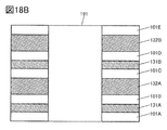
- an opening 191 is formed in the laminate 100 shown in FIG. 18A by resist mask forming, etching treatment, and the like.
- the resist mask can be formed by appropriately using a lithography method, a printing method, an inkjet method, or the like.
- the etching process may be a dry etching method or a wet etching method, or both may be used.
- the conductor 132A (conductor 132B) on the side surface of the opening 191 is removed by etching or the like, and a recess 192A (recess 192B) is formed on the side surface.
- the conductor 132A (conductor 132B) is a material (insulator 101A to 101E, and a conductor) from which the conductor 132A (conductor 132B) is selectively removed from the laminated body 100. It is assumed that a material having a higher etching rate than 131A (conductor 131B) is applied.
- a sacrificial layer is provided in the region where the opening 191 and the recess 192A (recess 192B) are formed at the stage of the manufacturing process of the semiconductor device shown in FIG. 18A, and the semiconductor shown in FIG. 18B is provided. It may be formed together with the opening 191 in the manufacturing process of the device. Further, when the opening 191 is formed without providing the sacrificial layer, the recess 192A (recess 192B) may be automatically formed.
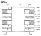
- the insulator 102 is formed on the side surface of the opening 191 shown in FIG. 19A and the recessed portion described above.
- the insulator 102 it is preferable to use an insulating material having a function of suppressing the permeation of oxygen.
- an insulating material having a function of suppressing the permeation of oxygen For example, it is preferable to use silicon nitride, silicon nitride, silicon oxide, aluminum nitride, aluminum nitride, or the like as the insulator 102.
- silicon nitride, silicon nitride, silicon oxide, aluminum nitride, aluminum nitride, or the like As the insulator 102, it is preferable to use an insulating material having a function of suppressing the permeation of oxygen.
- silicon nitride, silicon nitride, silicon oxide, aluminum nitride, aluminum nitride, or the like As the insulator 102, it is preferable to use an insulating material having a function of suppressing the permeation of oxygen.
- the conductor 133 is formed on the side surface of the opening 191 shown in FIG. 19B and the recess formed therein. That is, the conductor 133 is formed on the insulator 102.
- the conductor 133 a material applicable to the above-mentioned conductor 131A, conductor 131B, conductor 132A, and conductor 132B can be used. In particular, among the materials, it is preferable to apply a material having high conductivity to the conductor 133.
- the conductor 133 contained in the opening 191 is removed so that the conductor 133 remains only in the recesses described above by resist mask forming and etching treatment. As a result, the conductor 133a and the conductor 133b are formed. At this time, a part of the insulator 102 may be removed as long as the insulators 101A to 101E, the conductor 131A, and the conductor 131B are not exposed to the opening 191.
- the conductor 133a (conductor 133b) functions as the other electrode of the capacitance CS shown in FIG. 1A. That is, the capacitance CS is formed in the region 181A (region 181B) shown in FIG. 20B.
- the semiconductor 151 is formed on the insulator 102, the conductor 133a, and the conductor 133b located on the side surface of the opening 191.
- the semiconductor 151 a material containing one or more metal oxides selected from indium, element M (element M is, for example, aluminum, gallium, yttrium, tin, etc.) and zinc is applied. preferable.
- the insulator 102 in contact with the semiconductor 151 may use an insulating material having a function of suppressing the permeation of impurities such as water and hydrogen as well as oxygen. preferable.
- an insulator 102 By forming such an insulator 102, it is possible to prevent impurities such as water or hydrogen from entering through the insulator 102 and reacting with oxygen contained in the semiconductor 151 to become water.
- oxygen deficiency may be formed in the semiconductor 151. Impurities such as hydrogen may enter the oxygen deficiency to generate carriers as electrons.
- the transistor in which the region is included in the channel formation region tends to have a normally-on characteristic.
- an insulating material having a function of suppressing permeation of impurities such as water and hydrogen as well as oxygen as the insulator 102.
- the conductivity of the semiconductor 151 may differ depending on the formed region.
- the region in contact with the insulator 102 is shown as a region 151a and the region 151b
- the region in contact with the conductor 133a (conductor 133b) is shown as a region 151c. ..
- the region 151a is a region that overlaps with the side surface of the conductor 131A (conductor 131B)
- the region 151b is a region that overlaps with the side surface of the insulator 101A (insulator 101B to insulator 101E).
- the region 151c is in contact with the conductor 133a (conductor 133b), impurities such as hydrogen or water contained in the conductor 133a (conductor 133b) may diffuse into the region 151c. As described above, when impurities such as water or hydrogen are diffused in the semiconductor 151, electrons serving as carriers may be generated, so that the resistance of the region 151c may be lowered. Therefore, the region 151c is a region having higher conductivity than the regions 151a and 151b.
- Region 151a is a region serving as a transistor channel forming region. Therefore, when the transistor is in the ON state, the resistance of the region 151a is lowered, so that the conductivity is higher than that of the region 151b.
- the insulator 103 and the semiconductor 152 are sequentially formed on the semiconductor 151 located on the side surface of the opening 191.
- the insulator 103 a material applicable to the above-mentioned insulator 102 can be used.
- the insulator 103 is preferably an insulating material having a function of suppressing permeation of impurities such as water and hydrogen as well as oxygen.
- the transistor WTr shown in FIG. 1A is configured in the region 182A (region 182B) shown in FIG. 21B.
- the region 151a of the semiconductor 151 functions as a channel forming region of the transistor WTr
- each of the two regions 151b of the semiconductor 151 functions as a source electrode and a drain electrode of the transistor WTr.
- the conductor 132A functions as a gate electrode of the transistor WTr.
- the transistor WTr constitutes an oxide semiconductor (OS) transistor.
- the semiconductor 152 a material containing one or a plurality of metal oxides selected from indium, element M (element M is, for example, aluminum, gallium, yttrium, tin, etc.) and zinc is used as in semiconductor 151. be able to. Further, as an alternative to the semiconductor 152, a semiconductor material such as polycrystalline silicon or amorphous silicon can be used.
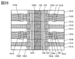
- the insulator 104 is formed on the semiconductor 152, and the conductor 134 is formed so as to fill the remaining opening 191.
- insulator 104 a material applicable to the above-mentioned insulator 102 and insulator 103 can be used.
- conductor 134 a material applicable to the above-mentioned conductor 131A, conductor 131B, conductor 132A, conductor 132B, conductor 133a, and conductor 133b can be used.
- the transistor RTr shown in FIG. 1A is configured.
- the region 151c of the semiconductor 151, the two regions 151b, and the conductor 133a (conductor 133b) function as the gate electrode of the transistor RTr
- the semiconductor 152 is the channel of the transistor RTr. It functions as a forming region
- the conductor 134 functions as a back gate electrode of the transistor RTr.
- the transistor RTr constitutes an OS transistor.
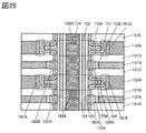
- the semiconductor device shown in FIG. 1A can be manufactured.
- One aspect of the present invention is not limited to the configuration example of the semiconductor device shown in FIG. 22A.
- One aspect of the present invention may have a configuration in which the semiconductor device shown in FIG. 22A is appropriately modified depending on the situation or as necessary.
- one aspect of the present invention may be a semiconductor device in which the transistor WTr and the transistor RTr are not provided with a back gate as shown in FIG. 1C.
- the step shown in FIG. 22B may be performed instead of the step shown in FIG. 22A in the process of manufacturing the semiconductor device shown in FIG. 1A.
- FIG. 22B shows a step of forming an insulator 105 so as to fill the opening 191 instead of the conductor 134 of FIG. 22A.
- the insulator 105 for example, a material applicable as the insulator 104 can be used.
- the configuration of the gate electrode of the transistor WTr may be changed from the configuration shown in FIG. 22A in order to improve the switching characteristics of the transistor WTr.
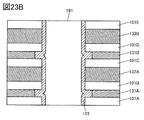
- 23A, 23B, 24A, and 24B show an example of a method for manufacturing the semiconductor device.
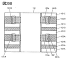
- FIG. 23A FIG. 18B shows a step in which the conductor 131A (conductor 131B) on the side surface of the opening 191 is removed to form the recess 193A (recess 193B).
- the conductor 131A (conductor 131B) is a material (conductor 132A (conductor 132B), insulator) from which the conductor 131A (conductor 131B) is selectively removed from the laminated body 100. It is assumed that a material having an etching rate higher than that of 101A to 101E is applied.
- the recess 193A (recess 193B) is shown in FIG. 18B by providing a sacrificial layer in the region where the opening 191 and the recess 193A (recess 193B) are formed at the stage of the manufacturing process of the semiconductor device shown in FIG. 18A. In the manufacturing process of the semiconductor device, it may be formed together with the opening 191. Further, when the opening 191 is formed without providing the sacrificial layer, the recess 193A (recess 193B) may be automatically formed.
- the semiconductor 153 is formed on the side surface of the opening 191 and the recess 193A (recess 193B) shown in FIG. 23A.
- the semiconductor 153 a material containing one or more metal oxides selected from indium, element M (element M is, for example, aluminum, gallium, yttrium, tin, etc.) and zinc is applied. To do.
- element M is, for example, aluminum, gallium, yttrium, tin, etc.
- the semiconductor 153 contained in the opening 191 is removed so that the semiconductor 153 remains only in the recess 193A (recess 193B) described above by resist mask forming and etching treatment, and the semiconductor 153a is removed. (Semiconductor 153b) is formed. Further, at the same time as this treatment or after this treatment, an etching treatment is performed to remove the conductor 132A (conductor 132B) to form the recess 192A (recess 192B).
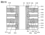
- the insulator 102 is formed on the side surface of the opening 191 so as to cover the semiconductor 153a (semiconductor 153b).
- the semiconductor 153a semiconductor 153b
- the semiconductor 153a semiconductor 153b comes into contact with the insulator 102, so that impurities such as hydrogen and water contained in the insulator 102 are removed from the semiconductor. It diffuses into 153a (semiconductor 153b).
- the semiconductor 153a semiconductor 153b
- the semiconductor 153a semiconductor 153b
- the semiconductor 153a semiconductor 153b
- the semiconductor 153a semiconductor 153b
- the semiconductor 153a has a low resistance and can function as a gate electrode of the transistor WTr.
- the semiconductor device shown in FIG. 24B can be configured by performing the same steps as those in FIGS. 21A to 22A.
- the transistor RTr in order to reduce the electrical resistance between the first terminal or the second terminal of the transistor WTr shown in FIG. 1A and the gate of the transistor RTr, the transistor RTr
- the configuration of the gate electrode may be changed from the configuration shown in FIG. 22A.
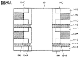
- 25A and 25B show an example of a method for manufacturing the semiconductor device.
- FIG. 25A not only the conductor 132A (conductor 132B) on the side surface of the opening 191 in FIG. 19A is removed, but also the insulator 101A to the insulator 101E are removed to remove the recess 194B (recess 194A, recess 194A, recess). It shows the process in which 194C) is formed.
- the conductor 132A (conductor 132B) and the insulator 101A to the insulator 101E are selectively removed from the laminated body 100. It is assumed that such a material (a material having a higher etching rate than the conductor 131A (conductor 131B)) is applied.
- the recess 194B (recess 194A, recess 194C) is provided with a sacrificial layer in the region where the opening 191 and the recess 194B (recess 194A, recess 194C) are formed at the stage of the manufacturing process of the semiconductor device shown in FIG. 18A.
- the semiconductor device may be formed together with the opening 191.
- the recess 194B (recess 194A, recess 194C) may be automatically formed.
- the conductor 132A (conductor 132B) is larger than the insulator 101B and the insulator 101C (insulator 101A, insulator 101D, insulator 101E). Although it is largely removed, the insulator 101B and the insulator 101C (insulator 101A, insulator 101D, insulator 101E) may be removed more than the conductor 132A (conductor 132B). Further, the insulator 101B, the insulator 101C (insulator 101A, the insulator 101D, the insulator 101E) and the conductor 132A (the conductor 132B) may be formed at the same depth.
- FIG. 25B shows a configuration example of a semiconductor device through the process of FIG. 25A.
- the conductor 133 is formed so as to fill the recess 194B (recess 194A, recess 194C), and the gate electrode of the transistor RTr is formed.
- the conductor 133a, the conductor 133b, and the conductor 133c that function as the gate electrodes of the transistor RTr are shown.
- the semiconductor device shown in FIG. 25B can be configured by performing the same steps from FIGS. 21A to 22A.
- This semiconductor device has a configuration in which the contact area between the semiconductor 151 and the conductor 133a (conductor 133b) is larger than that of the semiconductor device shown in FIG. 22A.
- the semiconductor device shown in FIG. 25B does not have the region 151b shown in FIG. 22A, so that the first terminal or the second terminal of the transistor WTr and the gate of the transistor RTr The electrical resistance between and can be reduced.
- FIGS. 26 to 28 are cross-sectional views for explaining a manufacturing example of the semiconductor device shown in FIG. 1A, similarly to FIGS. 18 to 22, and in particular, are cross-sectional views of the transistor WTr and the transistor RTr in the channel length direction. Shown. Further, in the cross-sectional views of FIGS. 26 to 28, as in FIGS. 18 to 22, some elements are omitted for the purpose of clarifying the drawings.
- FIG. 26A The process shown in FIG. 26A is a continuation of the process shown in FIG. 19B.
- the semiconductor 151 is formed on the side surface of the opening 191 shown in FIG. 19B and the recess formed therein. That is, the semiconductor 151 is formed on the insulator 102.
- the semiconductor 151 it is preferable to apply one or more semiconductors selected from indium, element M (element M is, for example, aluminum, gallium, yttrium, tin, etc.) and zinc.
- element M is, for example, aluminum, gallium, yttrium, tin, etc.
- the conductor 133 is formed on the side surface of the opening 191 shown in FIG. 26A and the recess formed therein.
- the description of the conductor 133 described in the manufacturing method example 1 is taken into consideration.
- the conductor 133 contained in the opening 191 is removed so that the conductor 133 remains only in the recesses described above by resist mask forming and etching treatment. As a result, the conductor 133a and the conductor 133b are formed. At this time, a part of the semiconductor 151 may be removed as long as the insulator 102 is not exposed to the opening 191.
- the conductor 133a (conductor 133b) functions as the other electrode of the capacitance CS shown in FIG. 1A. That is, the capacitance CS is formed in the region 181A (region 181B) shown in FIG. 27A.
- the description of the semiconductor 151 described in the manufacturing method example 1 is taken into consideration.
- the semiconductor 151 contains a metal oxide
- the semiconductor 151 can be divided into a region 151a, a region 151b, and a region 151c.
- the region 151a, the region 151b, and the region 151c the description of the region 151a, the region 151b, and the region 151c described in the production method example 1 is taken into consideration.
- the insulator 103 is formed on the conductor 133a, the conductor 133b, and the semiconductor 151 located on the side surface of the opening 191 and then the semiconductor 103 on the insulator 103. 152 is formed.
- the description of the insulator 103 described in the manufacturing method example 1 is taken into consideration.
- the transistor WTr shown in FIG. 1A is configured in the region 182A (region 182B) shown in FIG. 27B.
- the region 151a of the semiconductor 151 functions as a channel forming region of the transistor WTr
- each of the two regions 151b of the semiconductor 151 functions as a source electrode and a drain electrode of the transistor WTr.
- the conductor 132A functions as a gate electrode of the transistor WTr.
- the transistor WTr constitutes an OS transistor.
- the insulator 104 is formed on the semiconductor 152, and the conductor 134 is formed so as to fill the remaining opening 191.
- the description of the conductor 134 described in the manufacturing method example 1 is taken into consideration.
- the transistor RTr shown in FIG. 1A is configured.
- the region 151c of the semiconductor 151, the two regions 151b, and the conductor 133a (conductor 133b) function as the gate electrode of the transistor RTr
- the semiconductor 152 is the channel of the transistor RTr. It functions as a forming region
- the conductor 134 functions as a back gate electrode of the transistor RTr.
- the transistor RTr constitutes an OS transistor.
- the semiconductor device shown in FIG. 1A can be manufactured by performing the steps of FIGS. 18A to 19B and 26A to 28.
- One aspect of the present invention is not limited to the configuration example of the semiconductor device shown in FIG. 28.
- One aspect of the present invention may have a configuration in which the semiconductor device shown in FIG. 28 is appropriately modified depending on the situation or as necessary.
- one aspect of the present invention may be a semiconductor device in which the transistor WTr and the transistor RTr are not provided with a back gate as shown in FIG. 1C.
- an insulator is used so that the opening 191 is filled in the same manner as in the step shown in FIG. 22B.
- the film 105 may be formed (not shown).
- a material applicable as the insulator 104 can be used.
- the configuration of the gate electrode of the transistor WTr may be changed from the configuration shown in FIG. 28 in order to improve the switching characteristics of the transistor WTr.
- FIG. 29 shows a configuration example of the semiconductor device.
- the semiconductor 153a semiconductor 153b
- the semiconductor 153a semiconductor 153b
- the recess 193A reces 193B
- the insulator 102 is formed on the side surface of the opening 191 so as to cover the semiconductor 153a (semiconductor 153b).
- the semiconductor device shown in FIG. 29 can be configured by performing the same steps as in FIGS. 26A to 28.
- the description of FIGS. 23A, 23B, 24A, and 24B described in the production method example 1 is taken into consideration.
- FIG. 30 shows a configuration example of the semiconductor device.
- a configuration example shown in FIG. 25A described in Manufacturing Method Example 1 is manufactured.
- the semiconductor device shown in FIG. 30 can be configured by performing the same steps as in FIGS. 26A to 28.
- the description of FIG. 25B described in Production Method Example 1 is taken into consideration.
- a semiconductor device capable of holding a large amount of data can be manufactured by the above-mentioned manufacturing method example 1 or manufacturing method example 2.
- FIG. 31 shows a structure in which a cross-sectional view of the semiconductor device (circuit configuration of FIG. 1A) shown in FIG. 22A is applied to the region SD2 of the semiconductor device shown in FIG. 17B.
- the area SD1 corresponds to the memory cell MC.
- an opening is provided collectively in the structure in which the conductor which is the wiring RWL and the wiring WWL and the insulator are laminated, and the above-mentioned manufacturing method example 1 or manufacturing method example 2 is provided.
- the circuit configuration shown in FIG. 1A can be realized by manufacturing as described.
- peripheral circuits of a memory cell array such as a read circuit and a precharge circuit may be formed in the lower layer thereof.
- a Si transistor is formed on a silicon substrate or the like to form the peripheral circuit, and then, in the manufacturing method example 1 or the manufacturing method example 2, the semiconductor device of one aspect of the present invention is mounted on the peripheral circuit. It may be formed.
- FIG. 32A is a cross-sectional view in which the peripheral circuit is composed of a planar type Si transistor and the semiconductor device of one aspect of the present invention is formed on the upper layer thereof. Further, FIG.
- FIGS. 32A and 33A is a cross-sectional view in which the peripheral circuit is composed of a FIN type Si transistor and the semiconductor device of one aspect of the present invention is formed on the upper layer thereof.
- the semiconductor device shown in FIGS. 32A and 33A applies the configuration of FIG. 22A as an example.
- the Si transistors constituting the peripheral circuits are formed on the substrate 1700.
- the element separation layer 1701 is formed between a plurality of Si transistors.
- a conductor 1712 is formed as a source and a drain of the Si transistor.
- the conductor 1730 is formed so as to extend in the channel width direction, and is connected to another Si transistor or the conductor 1712 (not shown).
- a single crystal semiconductor substrate made of silicon or silicon carbide, a polycrystalline semiconductor substrate, a compound semiconductor substrate made of silicon germanium, an SOI substrate, or the like can be used.
- the substrate 1700 for example, a glass substrate, a quartz substrate, a plastic substrate, a metal substrate, a flexible substrate, a bonding film, paper containing a fibrous material, or a base film may be used. Further, a semiconductor element may be formed using a certain substrate, and then the semiconductor element may be transposed to another substrate.
- FIGS. 32A and 33A as an example, an example in which a single crystal silicon wafer is used for the substrate 1700 is shown.
- the planar type Si transistor shown in FIG. 32A shows a cross-sectional view in the channel length direction
- the planar type Si transistor shown in FIG. 32B shows a cross-sectional view in the channel width direction.
- the Si transistor is provided in contact with a channel forming region 1793 provided in the well 1792, a low concentration impurity region 1794, a high concentration impurity region 1795 (collectively referred to as an impurity region), and the impurity region.
- a metal silicide or the like may be used for the conductive region 1796.
- the FIN type Si transistor shown in FIG. 33A shows a cross-sectional view in the channel length direction
- the FIN type Si transistor shown in FIG. 33B shows a cross-sectional view in the channel width direction.
- the channel forming region 1793 has a convex shape
- a gate insulating film 1797 and a gate electrode 1790 are provided along the side surfaces and the upper surface thereof.
- the SOI substrate may be processed to form a semiconductor layer having a convex shape.
- the reference numerals shown in FIGS. 33A and 33B are the same as the reference numerals shown in FIGS. 32A and 32B.
- the insulator, conductor, semiconductor, etc. disclosed in the present specification and the like can be formed by a PVD (Physical Vapor Deposition) method and a CVD (Chemical Vapor Deposition) method.
- the PVD method include a sputtering method, a resistance heating vapor deposition method, an electron beam vapor deposition method, and a PLD (Pulsed Laser Deposition) method.
- the CVD method include a plasma CVD method and a thermal CVD method.
- examples of the thermal CVD method include a MOCVD (Metalorganic Chemical Vapor Deposition) method and an ALD (Atomic Layer Deposition) method.
- the thermal CVD method is a film forming method that does not use plasma, it has an advantage that defects are not generated due to plasma damage.
- the raw material gas and the oxidizing agent may be sent into the chamber at the same time, the inside of the chamber is set to atmospheric pressure or reduced pressure, and the film may be reacted by reacting in the vicinity of the substrate or on the substrate and depositing on the substrate. ..
- the inside of the chamber may be under atmospheric pressure or reduced pressure
- the raw material gas for the reaction is sequentially introduced into the chamber
- the film formation may be performed by repeating the order of gas introduction.
- each switching valve also called a high-speed valve
- the first raw material gas is not mixed at the same time or after that so that the multiple kinds of raw materials gas are not mixed.
- An active gas argon, nitrogen, etc. or the like is introduced, and a second raw material gas is introduced.
- the inert gas becomes a carrier gas, and the inert gas may be introduced at the same time when the second raw material gas is introduced.
- the first raw material gas may be discharged by vacuum exhaust, and then the second raw material gas may be introduced.
- the first raw material gas is adsorbed on the surface of the substrate to form a first thin layer, and reacts with the second raw material gas introduced later, so that the second thin layer is on the first thin layer.
- a thin film is formed by being laminated on.
- Thermal CVD methods such as the MOCVD method and the ALD method can form various films such as metal films, semiconductor films, and inorganic insulating films disclosed in the embodiments described so far, and for example, In-Ga-Zn.
- Trimethylindium (In (CH 3 ) 3 ), trimethylgallium (Ga (CH 3 ) 3 ), and dimethylzinc (Zn (CH 3 ) 2 ) are used to form a ⁇ O film.
- the combination is not limited to these, and triethylgallium (Ga (C 2 H 5 ) 3 ) can be used instead of trimethylgallium, and diethylzinc (Zn (C 2 H 5 ) 2 ) can be used instead of dimethylzinc. Can also be used.
- hafnium oxide film is formed by a film forming apparatus using ALD, a liquid containing a solvent and a hafnium precursor compound (hafnium alkoxide or tetrakisdimethylamide hafnium (TDHA, Hf [N (CH 3 ) 2 ]]. 4) a raw material gas hafnium amide) was vaporized, such as, using the two kinds of gases ozone (O 3) as an oxidizing agent.
- other materials include tetrakis (ethylmethylamide) hafnium and the like.
- a raw material gas obtained by vaporizing a liquid containing a solvent and an aluminum precursor compound (trimethylaluminum (TMA, Al (CH 3 ) 3), etc.)
- TMA trimethylaluminum
- H 2 O gases
- other materials include tris (dimethylamide) aluminum, triisobutylaluminum, aluminum tris (2,2,6,6-tetramethyl-3,5-heptane dinate) and the like.
- a silicon oxide film using a deposition apparatus employing ALD is hexachlorodisilane adsorbed on the film-forming surface, and supplying radicals for oxidizing gas (O 2, dinitrogen monoxide) adsorption React with things.
- oxidizing gas O 2, dinitrogen monoxide
- tungsten film when a tungsten film is formed by a film forming apparatus using ALD, WF 6 gas and B 2 H 6 gas are sequentially and repeatedly introduced to form an initial tungsten film, and then WF 6 gas and H 2 are formed. Gas is introduced repeatedly in sequence to form a tungsten film.
- SiH 4 gas may be used instead of B 2 H 6 gas.
- an oxide semiconductor film for example, an In-Ga-Zn-O film is formed by a film forming apparatus using ALD
- In (CH 3 ) 3 gas and O 3 gas are sequentially and repeatedly introduced into In.
- the ⁇ O layer is formed, and then Ga (CH 3 ) 3 gas and O 3 gas are sequentially and repeatedly introduced to form a GaO layer, and then Zn (CH 3 ) 2 gas and O 3 gas are sequentially and repeatedly introduced.
- Form a ZnO layer is not limited to this example.
- these gases may be used to form a mixed oxide layer such as an In—Ga—O layer, an In—Zn—O layer, and a Ga—Zn—O layer.
- O 3 may be used of H 2 O gas obtained by bubbling water with an inert gas such as Ar in place of the gas, but better to use an O 3 gas containing no H are preferred.
- In (C 2 H 5 ) 3 gas may be used instead of In (CH 3 ) 3 gas.
- Ga (C 2 H 5 ) 3 gas may be used instead of Ga (CH 3 ) 3 gas.
- Zn (CH 3 ) 2 gas may be used.
- FIGS. 34 to 40 are semiconductor devices (a part of the cross-sectional view of FIG. 22A) described in the second embodiment, and a method of driving the semiconductor device will be described with reference to these drawings.
- the same reference numerals are commonly used between different drawings for the same parts or parts having similar functions, and the repetition of the description will be omitted.
- the driving method of the semiconductor device the first embodiment can be incorporated.
- the semiconductor device will be described as a memory module.
- FIG. 34 is a diagram illustrating a memory module.
- the memory module includes a first memory cell, a second memory cell, a wiring BG, a wiring WL, a wiring RL, a wiring WWL [1], a wiring WWL [2], a wiring RWL [1], and a wiring RWL [ 2].
- the wiring WL and the wiring RL are semiconductor layers containing metal oxides. Further, the wiring WL has a region WL1 to a region WL9, and the wiring RL has a region RL1 to a region RL9.
- FIG. 34 shows an example in which the memory module has a first memory cell and a second memory cell, the number of memory cells that the memory module can have is not limited.
- the first memory cell has a read transistor RTr [1], a rewrite transistor WTr [1], and a capacitance CS [1]. Further, the second memory cell has a transistor RTr [2] for reading, a transistor WTr [2] for rewriting, and a capacitance CS [2].
- the gate electrode RTrG [1] of the transistor RTr [1] is located at a position overlapping the region WL2 and the region RL2. Further, the wiring WWL [1] that functions as a gate electrode of the transistor WTr [1] is located at a position that overlaps with the region WL4 and the region RL4. Similarly, the gate electrode RTrG [2] of the transistor RTr [2] is located at a position overlapping the region WL6 and the region RL6. Further, the wiring WWL [2] that functions as a gate electrode of the transistor WTr [2] is located at a position that overlaps with the region WL8 and the region RL8.
- the capacitance CS [1] is formed by arranging the gate electrode RTrG [1] of the transistor RTr [1] at a position where it overlaps with the wiring RWL [1] via the insulator 102. Therefore, the gate electrode RTRG [1] can be rephrased as the first memory node of the first memory cell. The data held in the first memory node is held in the capacity CS [1].
- the capacitance CS [2] is formed by arranging the gate electrode RTrG [2] of the transistor RTr [2] at a position where it overlaps with the wiring RWL [2] via the insulator 102. Therefore, the gate electrode RTRG [2] can be rephrased as the second memory node of the second memory cell. The data held in the second memory node is held in the capacity CS [2].
- the wiring BG has a region overlapping the wiring RL via the insulator 104, and the wiring RL has a region overlapping the wiring WL via the insulator 103.
- the wiring BG is arranged inside the wiring RL via the insulator 104, and the wiring RL is arranged inside the wiring WL via the insulator 103.
- the wiring BG has a region that functions as a back gate of the transistor RTr [1]. Further, the wiring BG can function the region RL1, the region RL3, the region RL4, the region RL5, the region RL7, the region RL8, and the region RL9 of the wiring RL as conductors.
- the region RL2 functions as a channel forming region of the transistor RTr [1], and the region RL6 functions as a channel forming region of the transistor RTr [2]. Further, the region RL4 functions as a back gate of the transistor WTr [1], and the region RL 8 functions as a back gate of the transistor WTr [2].
- the region RL1, the region RL3, the region RL5, the region RL7, and the region RL9 can make the region WL1, the region WL3, the region WL5, the region WL7, and the region WL9 function as conductors when a potential is applied.
- the resistance value is set by impurities such as hydrogen diffused from the insulating layer 101 (insulator 101A to 101E). It can function as a sag conductor.
- One of the source and drain of the selection transistor DTr1 is electrically connected to the wiring WBL1.
- the gate of the selection transistor DTr1 is electrically connected to the wiring WWL_D.
- the other of the source or drain of the selection transistor DTr1 is electrically connected to the gate electrode RTRG [1] that functions as the first memory node via the region WL1. It is preferable that the region WL1 is electrically connected to the gate electrode RTRG [1] via the region WL2.
- the gate electrode RTrG [1] is electrically connected to a region WL4 that functions as a channel forming region of the transistor WTr [1] via the region WL3.
- the gate electrode RTrG [1] is preferably electrically connected to the region WL3 via the region WL2.
- the area WL4 is electrically connected to the gate electrode RTrG [2] that functions as a second memory node via the area WL5. It is preferable that the region WL5 is electrically connected to the gate electrode RTrG [1] via the region WL6.
- the gate electrode RTrG [2] is electrically connected to a region WL8 that functions as a channel forming region of the transistor WTr [2] via the region WL7.
- the gate electrode RTrG [2] is preferably electrically connected to the region WL7 via the region WL6.
- the region WL8 is electrically connected to the wiring WBL1 via the region WL9 (not shown in FIG. 34).
- One of the source and drain of the selection transistor DTr2 is electrically connected to the wiring RBL2.
- the gate of the selection transistor DTr2 is electrically connected to the wiring RWL_D1.
- the other of the source or drain of the selected transistor DTr2 is electrically connected to the region RL2 which functions as a channel forming region of the transistor RTr [1] via the region RL1.
- the region RL2 is electrically connected to the region RL4 via the region RL3.
- the region RL4 functions as a back gate of the transistor WTr [1].
- the region RL4 is electrically connected to the region RL6 that functions as a channel forming region of the transistor RTr [2] via the region RL5.
- the region RL6 is electrically connected to the region RL8 via the region RL7.
- the region RL8 functions as a back gate of the transistor WTr [2].
- the region RL8 is electrically connected to one of the source and drain of the selection transistor DTr3 via the region RL9 (not shown in FIG. 34).
- the gate of the selection transistor DTr3 is electrically connected to the wiring RWL_D2.
- the region WL1 to the region WL9 can be suspended by using the selection transistor DTr1 and the transistor WTr [2]. Further, the region RL1 to the region RL9 can be put into a floating state by using the selection transistor DTr2 and the selection transistor DTr3.
- 35 to 40 are diagrams for explaining an operation example of the memory module.
- FIG. 35 describes, as an example, the operation of the data retention period of the memory cell of the memory module.
- the potential given to each wiring during the holding period is shown in the figure.
- the potential is an example and is not limited.
- F-4V it means that the wiring is in a floating state after -4V is applied to the wiring.
- F0V the wiring is in a floating state after 0V is applied to the wiring.
- the capacitance CS [1] or the capacitance CS [2] is given a potential of 0V to 3V as data. Further, -2V is given to the wiring BG. -4V is given from the wiring RBL2 to the region RL1 of the wiring RL via the selection transistor DTr2. Further, -4V is given from the wiring RBL1 to the region RL9 of the wiring RL via the selection transistor DTr3. After that, the selection transistor DTr2 and the selection transistor DTr3 are turned off, and the wiring RL is in a floating state. Further, 0V is given to the wiring WL from the wiring WBL1 via the selection transistor DTr1.
- the selection transistor DTr1 and the transistor WTr [2] are turned off, and the wiring WL is in a floating state. Further, the wiring WWL [1], the wiring RWL [1], the wiring WWL [2], and the wiring RWL [2] are given 0V and then enter a floating state.
- the wiring RBL1 and the wiring RBL2 may be in a floating state.
- the wiring WBL1 may be put in a floating state.
- the potential of the wiring BG By making the potential of the wiring BG larger than the potential of the wiring RL, the resistance value of the wiring RL formed by the semiconductor layer becomes smaller. Therefore, the potential of -4V given to the wiring RL is given to the region RL1, the region RL3, the region RL4, the region RL5, the region RL7, the region RL8, and the region RL9. At this time, a parasitic capacitance is formed between the wiring BG and the wiring RL via the insulator 104. That is, the potential difference given to the wiring BG and the wiring RL can be maintained in the parasitic capacitance by making the wiring RL float.
- the region RL4 and the region RL8 function as back gates for the transistor WTr [1] and the transistor WTr [2], the off-current of the transistor WTr [1] and the transistor WTr [2] can be reduced. It is preferable to give a potential smaller than the potential given to the wiring RL to the back gates of the selection transistor DTr1, the selection transistor DTr2, and the selection transistor DTr3.
- the wiring BG may be given a potential smaller than the potential given to the wiring RL.
- a potential smaller than the potential given to the wiring RL is applied to the wiring BG, the off-current of the transistor RTr [1] or the transistor RTr [2] can be reduced.
- the off-current of the transistor WTr [1] or the transistor WTr [2] can be reduced. Therefore, the retention period of the data stored in each memory node can be lengthened.
- FIG. 36 describes, as an example, the operation of the memory cell data rewriting period of the memory module.
- the potential given to each wiring during the rewriting period is shown in the figure.
- the potential is an example and is not limited.
- 0V is given from the wiring RBL2 to the region RL1 of the wiring RL via the selection transistor DTr2.
- 0V is given from the wiring RBL1 to the region RL9 of the wiring RL via the selection transistor DTr3.
- 3V is applied from the wiring WBL1 to the area WL1 or the area WL9 of the wiring WL via the selection transistor DTr1.
- 0V is applied from the wiring WBL1 to the area WL1 or the area WL9 of the wiring WL via the selection transistor DTr1.
- -2V is given to the wiring BG.
- the wiring WWL [1] is given -5V
- the wiring RWL [1] is given 0V
- the wiring WWL [2] is given 3V
- the wiring RWL [2] is given 0V.
- 3V is given to the wiring WWL [1]
- 0V is given to the wiring RWL [1]
- 3V is given to the wiring WWL [2]
- 0V is given to the wiring RWL [2].
- the wiring WWL [1] is given -5V
- the wiring RWL [1] is given 0V
- the wiring WWL [2] is given 3V
- the wiring RWL [2] is given 0V.
- the rewriting of the memory cell data included in the memory module described above may be rewritten via the area WL1.
- FIG. 37 describes, as an example, the operation of the data read period (non-selection) from the memory cell of the memory module.
- the potential given to each wiring during the read-out period is shown in the figure.
- the potential is an example and is not limited.
- 0V is applied to the region WL1 and the region WL9 of the wiring WL via the wiring WBL1, and then the region WL1 and the region WL9 are in a floating state. Further, it is preferable that the region RL1 of the wiring RL is given 3V via the wiring RBL2, and the region RL9 of the wiring RL is given 0V via the wiring RBL1 and then put into a floating state. In addition, -2V is given to the wiring BG.
- -5V is given to the wiring WWL [1] and the wiring WWL [2].
- the transistor WTr [1] is turned off.
- ⁇ 5V is applied to the wiring WWL [2]
- the transistor WTr [2] is turned off. Therefore, the data of the capacity CS [1] and the capacity CS [2] are retained.
- the potential held by the capacitance CS [1] changes from 0V to 3V due to the capacitive coupling of the capacitance CS [1].
- the potential held in the capacitance CS [1] is given to the gate of the transistor RTr [1]. Therefore, the transistor RTr [1] is turned on.
- the potential held by the capacitance CS [2] changes from 3V to 6V due to the capacitive coupling of the capacitance CS [2].
- the potential held by the capacitance CS [2] is given to the gate of the transistor RTr [2]. Therefore, the transistor RTr [2] is turned on.
- the transistor RTr [1] and the transistor RTr [2] are turned on regardless of the size of the data held in the capacitance CS. .. Therefore, when the memory cell included in the memory module is not selected, the potential given to the wiring RBL2 is output to the region RL9 possessed by the wiring RL.
- FIG. 38 describes the operation of the data read period (selection) from the memory cell of the memory module.
- the potential given to each wiring during the read-out period is shown in the figure.
- the potential is an example and is not limited. Note that FIG. 38 is different from FIG. 37 in that the potential applied to the wiring RWL [1] is 0 V. In addition, 0V is held in the capacity CS [1], and 3V is held in the capacity CS [2].
- 0V is given to the wiring RWL [1] as the memory cell to be read.
- the wiring RWL [1] is 0V, no capacitive coupling occurs via the capacitive CS [1]. Therefore, the potential held in the capacitance CS [1] is given to the gate of the transistor RTr [1]. Since the transistor RTr [1] maintains the off state, 0 V is maintained because the potential given to the wiring RBL2 is not output to the region RL9 of the wiring RL.
- 3V is given to the wiring RWL [2].
- the potential held by the capacitance CS [2] changes from 3V to 6V due to the capacitive coupling of the capacitance CS [2].
- the potential held by the capacitance CS [2] is given to the gate of the transistor RTr [2]. Therefore, the transistor RTr [2] is turned on.
- the potential given to the wiring RBL2 is output to the area RL9 of the wiring RL.
- the potential given to the wiring RBL2 does not change from 0V in the region RL9 of the wiring RL.
- FIG. 39 describes, as an example, the operation of shifting from the memory cell to the data read period to the retention period of the memory module.
- the potential given to each wiring during the read-out period and the change in potential at the time of transition are shown in the figure.
- the potential is an example and is not limited.
- -2V is given to the wiring BG.
- 0V is given to the wiring RWL [1] and the wiring RWL [2].
- 0V is held in the capacity CS [1]
- 3V is held in the capacity CS [2].
- the potential given to the region RL1 and the region RL9 of the wiring RL is changed from 3V to -3V.
- the wiring WWL [1] and the wiring WWL [2] are changed from ⁇ 5V to 0V.
- the wiring RWL [1] and the wiring RWL [2] are changed from 3V to 0V.
- the wiring RL, the wiring RWL [1], the wiring RWL [2], the wiring WWL [1], and the wiring WWL [2] are put into a floating state. Since the transistor RTr and the transistor WTr are OS transistors, the off-current is small.
- the capacitance CS [1] and the capacitance even if the wiring RL, the wiring RWL [1], the wiring RWL [2], the wiring WWL [1], and the wiring WWL [2] are in a floating state.
- the data held in CS [2] can suppress deterioration.
- FIG. 40 describes, as an example, the operation of shifting from the memory cell to the data rewriting period to the retention period of the memory module.
- the potential is an example and is not limited.
- -2V is given to the wiring BG.
- 0V is given to the wiring RWL [1] and the wiring RWL [2].
- 0V is held in the capacity CS [1]
- 3V is held in the capacity CS [2].
- the potential given to the region WL1 and the region WL9 of the wiring WL is changed from 0V to -3V.
- the wiring WWL [1] is changed from ⁇ 5V to 0V
- the wiring WWL [2] is changed from 3V to 0V.
- the wiring WL, the wiring WWL [1], the wiring WWL [2], the wiring RWL [1], and the wiring RWL [2] are put into a floating state. Since the transistor RTr and the transistor WTr are OS transistors, the off-current is small.
- the data held in CS [2] can suppress deterioration.
- FIG. 41 is a block diagram showing an example configuration of a CPU using the semiconductor device described in the first embodiment as a part.
- the CPU shown in FIG. 41 has an ALU 1191 (ALU: Arithmetic logic unit, arithmetic unit), an ALU controller 1192, an instruction decoder 1193, an interrupt controller 1194, a timing controller 1195, a register 1196, a register controller 1197, and a bus interface 1198 on a substrate 1190. It has (Bus I / F), a rewritable ROM 1199, and a ROM interface 1189 (ROM I / F).
- the substrate 1190 a semiconductor substrate, an SOI substrate, a glass substrate, or the like is used.
- the ROM 1199 and the ROM interface 1189 may be provided on separate chips.
- the configuration including the CPU or the arithmetic circuit shown in FIG. 41 may be one core, and a configuration including a plurality of the cores and each core operating in parallel, that is, a configuration such as a GPU may be used.
- the number of bits that the CPU can handle in the internal arithmetic circuit or the data bus can be, for example, 8 bits, 16 bits, 32 bits, 64 bits, or the like.
- Instructions input to the CPU via the bus interface 1198 are input to the instruction decoder 1193, decoded, and then input to the ALU controller 1192, interrupt controller 1194, register controller 1197, and timing controller 1195.
- the ALU controller 1192, interrupt controller 1194, register controller 1197, and timing controller 1195 perform various controls based on the decoded instructions. Specifically, the ALU controller 1192 generates a signal for controlling the operation of the ALU 1191. Further, the interrupt controller 1194 determines and processes an interrupt request from an external input / output device or a peripheral circuit from the priority or the mask state during the execution of the CPU program. The register controller 1197 generates the address of the register 1196 and reads or writes the register 1196 according to the state of the CPU.
- the timing controller 1195 generates a signal for controlling the operation timing of the ALU 1191, the ALU controller 1192, the instruction decoder 1193, the interrupt controller 1194, and the register controller 1197.
- the timing controller 1195 includes an internal clock generator that generates an internal clock signal based on the reference clock signal, and supplies the internal clock signal to the above-mentioned various circuits.
- a memory cell is provided in the register 1196.
- the transistor shown in the previous embodiment can be used as the memory cell of the register 1196.
- the register controller 1197 selects the holding operation in the register 1196 according to the instruction from the ALU 1191. That is, in the memory cell of the register 1196, it is selected whether to hold the data by the flip-flop or the data by the capacity. When holding data by flip-flop is selected, the power supply voltage is supplied to the memory cell in the register 1196. When the retention of data in the capacitance is selected, the data is rewritten to the capacitance and the supply of the power supply voltage to the memory cell in the register 1196 can be stopped.
- the storage device of the above embodiment can be applied to various removable storage devices such as a memory card (for example, an SD card), a USB (Universal Serial Bus) memory, and an SSD (Solid State Drive).
- a memory card for example, an SD card
- USB Universal Serial Bus
- SSD Solid State Drive
- FIG. 42A is a schematic diagram of a USB memory.
- the USB memory 5100 has a housing 5101, a cap 5102, a USB connector 5103, and a board 5104.
- the substrate 5104 is housed in the housing 5101.
- the substrate 5104 is provided with a storage device and a circuit for driving the storage device.
- a memory chip 5105 and a controller chip 5106 are attached to the substrate 5104.
- the memory chip 5105 incorporates the memory cell array 2610, the word line driver circuit 2622, the low decoder 2621, the sense amplifier 2633, the precharge circuit 2632, the column decoder 2631, and the like described in the second embodiment.
- the controller chip 5106 incorporates a processor, a work memory, an ECC circuit, and the like.
- the circuit configurations of the memory chip 5105 and the controller chip 5106 are not limited to the above description, and the circuit configurations may be appropriately changed depending on the situation or in some cases.
- the word line driver circuit 2622, the low decoder 2621, the sense amplifier 2633, the precharge circuit 2632, and the column decoder 2631 may be incorporated in the controller chip 5106 instead of the memory chip 5105.
- the USB connector 5103 functions as an interface for connecting to an external device.
- FIG. 42B is a schematic view of the appearance of the SD card
- FIG. 42C is a schematic view of the internal structure of the SD card.
- the SD card 5110 has a housing 5111, a connector 5112, and a substrate 5113.
- the connector 5112 functions as an interface for connecting to an external device.
- the substrate 5113 is housed in the housing 5111.
- the substrate 5113 is provided with a storage device and a circuit for driving the storage device. For example, a memory chip 5114 and a controller chip 5115 are attached to the substrate 5113.
- the memory chip 5114 incorporates the memory cell array 2610, the word line driver circuit 2622, the low decoder 2621, the sense amplifier 2633, the precharge circuit 2632, the column decoder 2631, and the like described in the second embodiment.
- the controller chip 5115 incorporates a processor, a work memory, an ECC circuit, and the like.
- the circuit configurations of the memory chip 5114 and the controller chip 5115 are not limited to the above description, and the circuit configurations may be appropriately changed depending on the situation or in some cases.
- the word line driver circuit 2622, the low decoder 2621, the sense amplifier 2633, the precharge circuit 2632, and the column decoder 2631 may be incorporated in the controller chip 5115 instead of the memory chip 5114.
- the capacity of the SD card 5110 can be increased. Further, a wireless chip having a wireless communication function may be provided on the substrate 5113. As a result, wireless communication can be performed between the external device and the SD card 5110, and data on the memory chip 5114 can be read and written.
- FIG. 42D is a schematic view of the appearance of the SSD
- FIG. 42E is a schematic view of the internal structure of the SSD.
- the SSD 5150 has a housing 5151, a connector 5152, and a substrate 5153.
- the connector 5152 functions as an interface for connecting to an external device.
- the substrate 5153 is housed in the housing 5151.
- the substrate 5153 is provided with a storage device and a circuit for driving the storage device. For example, a memory chip 5154, a memory chip 5155, and a controller chip 5156 are attached to the substrate 5153.
- the memory chip 5154 incorporates the memory cell array 2610, the word line driver circuit 2622, the low decoder 2621, the sense amplifier 2633, the precharge circuit 2632, the column decoder 2631, and the like described in the second embodiment.
- a work memory is incorporated in the memory chip 5155.
- a DRAM chip may be used as the memory chip 5155.
- a processor, an ECC circuit, and the like are incorporated in the controller chip 5156.
- the circuit configurations of the memory chip 5154, the memory chip 5155, and the controller chip 5115 are not limited to the above description, and the circuit configurations may be appropriately changed depending on the situation or in some cases. ..
- the controller chip 5156 may also be provided with a memory that functions as a work memory.
- FIG. 43A is a notebook personal computer, which includes a housing 5401, a display unit 5402, a keyboard 5403, a pointing device 5404, and the like.
- the storage device of one aspect of the present invention can be provided in a notebook personal computer.
- FIG. 43B is a smart watch which is a kind of wearable terminal, and has a housing 5901, a display unit 5902, an operation button 5903, an operator 5904, a band 5905, and the like.
- the storage device of one aspect of the present invention can be provided in a smart watch.
- the display unit 5902 may use a display device having a function as a position input device.
- the function as a position input device can be added by providing a touch panel on the display device.
- the function as a position input device can be added by providing a photoelectric conversion element, which is also called a photo sensor, in the pixel portion of the display device.
- the operation button 5903 may be provided with any one of a power switch for activating the smartwatch, a button for operating the smartwatch application, a volume adjustment button, and a switch for turning on or off the display unit 5902.
- the number of operation buttons 5903 is shown as two, but the number of operation buttons included in the smart watch is not limited to this.
- the operator 5904 functions as a crown for adjusting the time of the smart watch. Further, the operator 5904 may be used as an input interface for operating the smartwatch application in addition to the time adjustment.
- the smart watch shown in FIG. 43B has a configuration having an operator 5904, but the present invention is not limited to this, and a configuration without an operator 5904 may be used.
- FIG. 43C is a video camera, which includes a first housing 5801, a second housing 5802, a display unit 5803, an operation key 5804, a lens 5805, a connection unit 5806, and the like.
- the storage device of one aspect of the present invention can be provided in a video camera.
- the operation key 5804 and the lens 5805 are provided in the first housing 5801
- the display unit 5803 is provided in the second housing 5802.
- the first housing 5801 and the second housing 5802 are connected by a connecting portion 5806, and the angle between the first housing 5801 and the second housing 5802 can be changed by the connecting portion 5806. is there.
- the image on the display unit 5803 may be switched according to the angle between the first housing 5801 and the second housing 5802 on the connecting unit 5806.
- FIG. 43D is a mobile phone having a function of an information terminal, which includes a housing 5501, a display unit 5502, a microphone 5503, a speaker 5504, and an operation button 5505.
- the storage device of one aspect of the present invention can be provided in a mobile phone.
- the display unit 5502 may use a display device having a function as a position input device.
- the function as a position input device can be added by providing a touch panel on the display device.
- the function as a position input device can be added by providing a photoelectric conversion element, which is also called a photo sensor, in the pixel portion of the display device.
- the operation button 5505 may be provided with any one of a power switch for activating the mobile phone, a button for operating the application of the mobile phone, a volume adjustment button, and a switch for turning on or off the display unit 5502.
- the number of operation buttons 5505 is shown as two, but the number of operation buttons possessed by the mobile phone is not limited to this.
- the mobile phone shown in FIG. 43D may have a flashlight or a light emitting device for lighting purposes.
- FIG. 43E is a perspective view showing the television device.
- the television device includes a housing 9000, a display unit 9001, a speaker 9003, an operation key 9005 (including a power switch or an operation switch), a connection terminal 9006, and a sensor 9007 (force, displacement, position, speed, acceleration, angular velocity, rotation). Includes the ability to measure numbers, distances, light, liquids, magnetism, temperature, chemicals, voice, time, hardness, electric fields, currents, voltages, power, radiation, flow rates, humidity, gradients, vibrations, odors or infrared rays) And so on.
- the storage device of one aspect of the present invention can be provided in the television device.
- the television device can incorporate a large screen, for example, a display unit 9001 having a size of 50 inches or more, or 100 inches or more.
- the above-mentioned storage device can also be applied around the driver's seat of a moving vehicle.
- FIG. 43F is a diagram showing the periphery of the windshield in the interior of an automobile.
- a display panel 5701 attached to the dashboard a display panel 5702, a display panel 5703, and a display panel 5704 attached to the pillar are shown.
- the display panel 5701 to the display panel 5703 can provide various information by displaying navigation information, a speedometer or tachometer, a mileage, a fuel gauge, a gear status, an air conditioner setting, and the like.
- the display items and layout displayed on the display panel can be appropriately changed according to the user's preference, and the design can be improved.
- the display panel 5701 to 5703 can also be used as a lighting device.
- the field of view (blind spot) blocked by the pillars can be complemented. That is, by displaying the image from the imaging means provided on the outside of the automobile, the blind spot can be supplemented and the safety can be enhanced. In addition, by projecting an image that complements the invisible part, safety confirmation can be performed more naturally and without discomfort.
- the display panel 5704 can also be used as a lighting device.
- the storage device of one aspect of the present invention can be provided in a moving body.
- the storage device according to one aspect of the present invention is, for example, a frame memory for temporarily storing image data used when displaying an image on the display panel 5701 to 5704, or a program for driving a system included in a moving body. It can be used as a storage device or the like for storing.
- the electronic devices shown in FIGS. 43A to 43C, 43E, and 43F may have a microphone and a speaker.
- the above-mentioned electronic device can be provided with a voice input function.
- the electronic devices shown in FIGS. 43A, 43B, 43D to 43F may have a camera.
- the electronic devices shown in FIGS. 43A to 43F have sensors (force, displacement, position, speed, acceleration, angular velocity, rotation speed, distance, light, liquid, magnetism, etc.) inside the housing. It may have a configuration (including a function of measuring temperature, chemical substance, sound, time, hardness, electric field, current, voltage, power, radiation, flow rate, humidity, inclination, vibration, odor, infrared ray, etc.).
- a detection device having a sensor for detecting inclination such as a gyro and an acceleration sensor, the orientation of the mobile phone (which direction the mobile phone faces with respect to the vertical direction).
- the screen display of the display unit 5502 can be automatically switched according to the orientation of the mobile phone.
- the electronic devices shown in FIGS. 43A to 43F may have a device for acquiring biological information such as fingerprints, veins, irises, or voiceprints. By applying this configuration, an electronic device having a biometric authentication function can be realized.
- a flexible base material may be used as a display unit of the electronic device shown in FIGS. 43A to 43F.
- the display unit may be configured such that a transistor, a capacitance, a display element, and the like are provided on a flexible base material.
- the content (may be a part of the content) described in one embodiment is the other content (may be a part of the content) described in the embodiment and one or more other implementations. It is possible to apply, combine, or replace at least one content with the content described in the form of (may be a part of the content).
- the figure (which may be a part) described in one embodiment is different from another part of the figure, another figure (which may be a part) described in the embodiment, and one or more other figures.
- the diagram (which may be a part) described in the embodiment By combining at least one diagram with the diagram (which may be a part) described in the embodiment, more diagrams can be constructed.
- ordinal numbers “first”, “second”, and “third” are added to avoid confusion of the components. Therefore, the number of components is not limited. Moreover, the order of the components is not limited. Further, for example, the component referred to in “first” in one of the embodiments of the present specification and the like is defined as a component referred to in “second” in another embodiment or in the claims. It is possible. Further, for example, the component referred to in “first” in one of the embodiments of the present specification and the like may be omitted in another embodiment or in the claims.
- the terms “above” and “below” do not limit the positional relationship of the components directly above or below and in direct contact with each other.
- the electrode B does not have to be formed in direct contact with the insulating layer A, and another configuration is formed between the insulating layer A and the electrode B. Do not exclude those that contain elements.
- the size, the thickness of the layer, or the area is shown in an arbitrary size for convenience of explanation. Therefore, it is not necessarily limited to that scale.
- the drawings are schematically shown for the sake of clarity, and are not limited to the shapes or values shown in the drawings. For example, it is possible to include variations in signal, voltage, or current due to noise, or variations in signal, voltage, or current due to timing lag.
- the channel forming region refers to a region where a channel is formed by applying an electric potential to the gate, and by forming this region, a current can flow between the source and the drain. it can.
- source and drain functions may be interchanged when transistors with different polarities are used or when the direction of current changes during circuit operation. Therefore, in the present specification and the like, the terms source and drain can be used interchangeably.
- the transistor described in the present specification or the like has two or more gates (this configuration may be referred to as a dual gate structure), those gates may be referred to as a first gate and a second gate, or a front gate. , Sometimes called a back gate.
- the phrase “front gate” can simply be paraphrased into the phrase “gate”.
- the phrase “backgate” can simply be paraphrased into the phrase “gate”.
- the bottom gate refers to a terminal formed before the channel formation region when the transistor is manufactured, and the "top gate” is formed after the channel formation region when the transistor is manufactured. Transistor terminal.
- electrode and “wiring” in the present specification and the like do not functionally limit these components.
- an “electrode” may be used as part of a “wiring” and vice versa.
- the terms “electrode” and “wiring” include the case where a plurality of “electrodes” and “wiring” are integrally formed.
- the voltage and the potential can be paraphrased as appropriate.
- the voltage is a potential difference from a reference potential.
- the reference potential is a ground potential (ground potential)
- the voltage can be paraphrased as a potential.
- the ground potential does not necessarily mean 0V.
- the electric potential is relative, and the electric potential given to the wiring or the like may be changed depending on the reference electric potential.
- membrane and layer can be interchanged with each other in some cases or depending on the situation.
- terms such as “wiring”, “signal line”, and “power line” can be interchanged with each other in some cases or depending on the situation.
- the reverse is also true, and it may be possible to change terms such as “signal line” and “power line” to the term “wiring”.
- a term such as “power line” may be changed to a term such as "signal line”.
- terms such as “signal line” may be changed to terms such as "power line”.
- the term “potential” applied to the wiring may be changed to a term such as “signal” in some cases or depending on the situation.
- the reverse is also true, and terms such as “signal” may be changed to the term “potential”.
- the semiconductor impurities are, for example, other than the main components constituting the semiconductor layer.
- an element having a concentration of less than 0.1 atomic% is an impurity. Due to the inclusion of impurities, for example, DOS (Density of States) may be formed in the semiconductor, carrier mobility may be lowered, crystallinity may be lowered, and the like.
- the impurities that change the characteristics of the semiconductor include, for example, group 1 element, group 2 element, group 13 element, group 14 element, group 15 element, and other than the main component.
- transition metals and the like and in particular, hydrogen (also contained in water), lithium, sodium, silicon, boron, phosphorus, carbon, nitrogen and the like.
- oxygen deficiency may be formed due to the mixing of impurities such as hydrogen.
- the impurities that change the characteristics of the semiconductor include, for example, Group 1 elements other than oxygen and hydrogen, Group 2 elements, Group 13 elements, Group 15 elements and the like.
- a switch means a switch that is in a conductive state (on state) or a non-conducting state (off state) and has a function of controlling whether or not a current flows.
- the switch means a switch having a function of selecting and switching a path through which a current flows.
- an electric switch or a mechanical switch can be used. That is, the switch is not limited to a specific switch as long as it can control the current.
- Examples of electrical switches include transistors (for example, bipolar transistors, MOS transistors, etc.), diodes (for example, PN diodes, PIN diodes, Schottky diodes, MIM (Metal Insulator Metal) diodes, and MIS (Metal Insulator Semiconductor) diodes. , Diode-connected transistors, etc.), or logic circuits that combine these.
- transistors for example, bipolar transistors, MOS transistors, etc.
- diodes for example, PN diodes, PIN diodes, Schottky diodes, MIM (Metal Insulator Metal) diodes, and MIS (Metal Insulator Semiconductor) diodes. , Diode-connected transistors, etc.
- diodes for example, PN diodes, PIN diodes, Schottky diodes, MIM (Metal Insulator Metal) diodes, and MIS (Metal Insulator Semiconductor) diodes. , Diode
- the "conducting state” of the transistor means a state in which the source electrode and the drain electrode of the transistor can be regarded as being electrically short-circuited. Further, the “non-conducting state” of the transistor means a state in which the source electrode and the drain electrode of the transistor can be regarded as being electrically cut off.
- the polarity (conductive type) of the transistor is not particularly limited.
- a mechanical switch is a switch that uses MEMS (Micro Electro Mechanical System) technology, such as the Digital Micromirror Device (DMD).
- MEMS Micro Electro Mechanical System
- DMD Digital Micromirror Device
- the switch has an electrode that can be moved mechanically, and by moving the electrode, it operates by controlling conduction and non-conduction.
- connection ⁇ About connection
- X and Y are connected, the case where X and Y are electrically connected and the case where X and Y are functionally connected. And the case where X and Y are directly connected. Therefore, it is not limited to the predetermined connection relationship, for example, the connection relationship shown in the figure or text, and includes the connection relationship other than the connection relationship shown in the figure or text.
- X, Y, etc. are objects (for example, devices, elements, circuits, wirings, electrodes, terminals, conductive films, layers, etc.).
- an element that enables an electrical connection between X and Y for example, a switch, a transistor, a capacitance, an inductor, a resistance element, a diode, and a display element
- Light emitting element, load, etc. can be connected to one or more between X and Y.
- the switch has a function of controlling on / off. That is, the switch is in a conductive state (on state) or a non-conducting state (off state), and has a function of controlling whether or not a current flows.
- a circuit that enables functional connection between X and Y for example, a logic circuit (inverter, NAND circuit, NOR circuit, etc.), signal conversion) Circuits (DA conversion circuit, AD conversion circuit, gamma correction circuit, etc.), potential level conversion circuit (power supply circuit (boost circuit, step-down circuit, etc.), level shifter circuit that changes the signal potential level, etc.), voltage source, current source, switching Circuits, amplification circuits (circuits that can increase signal amplitude or current amount, operational amplifiers, differential amplification circuits, source follower circuits, buffer circuits, etc.), signal generation circuits, storage circuits, control circuits, etc.) are X and Y. It is possible to connect one or more in between. As an example, even if another circuit is sandwiched between X and Y, if the signal output from X is transmitted to Y, it is assumed that X and Y are functionally connected. To do.
- X and Y are electrically connected, it means that X and Y are electrically connected (that is, another element between X and Y). Or when they are connected with another circuit in between) and when X and Y are functionally connected (that is, they are functionally connected with another circuit in between X and Y). (Is) and the case where X and Y are directly connected (that is, the case where another element or another circuit is not sandwiched between X and Y) is included. In other words, the case of explicitly stating that it is electrically connected is the same as the case of explicitly stating that it is simply connected.
- the source of the transistor (or the first terminal, etc.) is electrically connected to X via (or not) Z1, and the drain of the transistor (or the second terminal, etc.) connects to Z2.
- the source of the transistor or the first terminal, etc.
- the source of the transistor is directly connected to one part of Z1 and another part of Z1.
- the drain of the transistor is directly connected to one part of Z2, and another part of Z2 is directly connected to Y.
- X and Y the source of the transistor (or the first terminal, etc.) and the drain (or the second terminal, etc.) are electrically connected to each other, and the X, the source of the transistor (or the first terminal, etc.) (Terminals, etc.), transistor drains (or second terminals, etc.), and Y are electrically connected in this order.
- the source of the transistor (or the first terminal, etc.) is electrically connected to X
- the drain of the transistor (or the second terminal, etc.) is electrically connected to Y
- the first terminal, etc.), the drain of the transistor (or the second terminal, etc.), and Y are electrically connected in this order.
- X is electrically connected to Y via the source (or first terminal, etc.) and drain (or second terminal, etc.) of the transistor, and X, the source (or first terminal, etc.) of the transistor.
- the terminals, etc.), the drain of the transistor (or the second terminal, etc.), and Y are provided in this connection order.
- the source (or first terminal, etc.) and drain (or second terminal, etc.) of the transistor can be separated. Separately, the technical scope can be determined. It should be noted that these expression methods are examples and are not limited to these expression methods.
- X, Y, Z1 and Z2 are objects (for example, devices, elements, circuits, wirings, electrodes, terminals, conductive films, layers, etc.).
- the circuit diagram shows that the independent components are electrically connected to each other, the case where one component has the functions of a plurality of components together.
- one component has the functions of a plurality of components together.
- the electrical connection in the present specification also includes the case where one conductive film has the functions of a plurality of components in combination.
- parallel means a state in which two straight lines are arranged at an angle of ⁇ 10 ° or more and 10 ° or less. Therefore, the case of ⁇ 5 ° or more and 5 ° or less is also included.
- substantially parallel means a state in which two straight lines are arranged at an angle of ⁇ 30 ° or more and 30 ° or less.
- vertical means a state in which two straight lines are arranged at an angle of 80 ° or more and 100 ° or less. Therefore, the case of 85 ° or more and 95 ° or less is also included.
- substantially vertical means a state in which two straight lines are arranged at an angle of 60 ° or more and 120 ° or less.
- DM1 Region, DM2: Region, DTr1: Selective Conductor, DTr2: Selective Conductor, DTr3: Selective Conductor, RBL1: Wiring, RBL2: Wiring, RL1: Region, RL2: Region, RL3: Region, RL4: Region, RL5: Region , RL6: region, RL7: region, RL8: region, RL9: region, RW2: region, RW4: region, RW6: region, RW8: region, RWL_D1: wiring, RWL_D2: wiring, WWL_D: wiring, SD1: region, SD2 : Area, WBL1: Wiring, WBL1a: Wiring, WBL2: Wiring, WL1: Area, WL2: Area, WL3: Area, WL4: Area, WL5: Area, WL6: Area, WL7: Area, WL8: Area, WL9: Area , WLR9: region, WWL4
Landscapes
- Engineering & Computer Science (AREA)
- Microelectronics & Electronic Packaging (AREA)
- Computer Hardware Design (AREA)
- Semiconductor Memories (AREA)
- Metal-Oxide And Bipolar Metal-Oxide Semiconductor Integrated Circuits (AREA)
- Thin Film Transistor (AREA)
Priority Applications (3)
| Application Number | Priority Date | Filing Date | Title |
|---|---|---|---|
| JP2021541742A JP7630430B2 (ja) | 2019-08-29 | 2020-08-17 | 半導体装置、電子機器 |
| US17/634,270 US20220328487A1 (en) | 2019-08-29 | 2020-08-17 | Semiconductor device and electronic device |
| JP2025016608A JP2025069338A (ja) | 2019-08-29 | 2025-02-04 | 半導体装置 |
Applications Claiming Priority (4)
| Application Number | Priority Date | Filing Date | Title |
|---|---|---|---|
| JP2019156245 | 2019-08-29 | ||
| JP2019-156245 | 2019-08-29 | ||
| JP2019-220154 | 2019-12-05 | ||
| JP2019220154 | 2019-12-05 |
Publications (1)
| Publication Number | Publication Date |
|---|---|
| WO2021038363A1 true WO2021038363A1 (ja) | 2021-03-04 |
Family
ID=74683610
Family Applications (1)
| Application Number | Title | Priority Date | Filing Date |
|---|---|---|---|
| PCT/IB2020/057716 Ceased WO2021038363A1 (ja) | 2019-08-29 | 2020-08-17 | 半導体装置、電子機器 |
Country Status (3)
| Country | Link |
|---|---|
| US (1) | US20220328487A1 (https=) |
| JP (2) | JP7630430B2 (https=) |
| WO (1) | WO2021038363A1 (https=) |
Families Citing this family (3)
| Publication number | Priority date | Publication date | Assignee | Title |
|---|---|---|---|---|
| KR20230074757A (ko) | 2020-10-02 | 2023-05-31 | 가부시키가이샤 한도오따이 에네루기 켄큐쇼 | 반도체 장치 |
| KR20230106849A (ko) * | 2022-01-07 | 2023-07-14 | 삼성전자주식회사 | 반도체 장치 |
| CN116206643B (zh) * | 2022-07-25 | 2024-03-15 | 北京超弦存储器研究院 | 动态随机存储单元、存储器、存储装置及读取方法 |
Citations (4)
| Publication number | Priority date | Publication date | Assignee | Title |
|---|---|---|---|---|
| JP2017168809A (ja) * | 2015-10-22 | 2017-09-21 | 株式会社半導体エネルギー研究所 | 半導体装置、又は該半導体装置を有する記憶装置 |
| JP2018157208A (ja) * | 2017-03-16 | 2018-10-04 | 東芝メモリ株式会社 | 半導体メモリ |
| JP2018206828A (ja) * | 2017-05-31 | 2018-12-27 | 株式会社半導体エネルギー研究所 | 半導体装置、および半導体装置の作製方法 |
| JP2019008862A (ja) * | 2017-06-26 | 2019-01-17 | 株式会社半導体エネルギー研究所 | 半導体装置、電子機器 |
Family Cites Families (8)
| Publication number | Priority date | Publication date | Assignee | Title |
|---|---|---|---|---|
| JPS63121194A (ja) * | 1986-11-11 | 1988-05-25 | Hitachi Ltd | 半導体記憶装置 |
| US7710765B2 (en) * | 2007-09-27 | 2010-05-04 | Micron Technology, Inc. | Back gated SRAM cell |
| WO2011081000A1 (en) * | 2009-12-28 | 2011-07-07 | Semiconductor Energy Laboratory Co., Ltd. | Memory device and semiconductor device |
| US8588000B2 (en) * | 2010-05-20 | 2013-11-19 | Semiconductor Energy Laboratory Co., Ltd. | Semiconductor memory device having a reading transistor with a back-gate electrode |
| US8902637B2 (en) * | 2010-11-08 | 2014-12-02 | Semiconductor Energy Laboratory Co., Ltd. | Semiconductor memory device comprising inverting amplifier circuit and driving method thereof |
| US9998119B2 (en) * | 2016-05-20 | 2018-06-12 | Semiconductor Energy Laboratory Co., Ltd. | Semiconductor device, electronic component, and electronic device |
| KR20180055701A (ko) * | 2016-11-17 | 2018-05-25 | 가부시키가이샤 한도오따이 에네루기 켄큐쇼 | 반도체 장치 및 반도체 장치의 제작 방법 |
| US10497712B2 (en) * | 2017-03-16 | 2019-12-03 | Toshiba Memory Corporation | Semiconductor memory |
-
2020
- 2020-08-17 WO PCT/IB2020/057716 patent/WO2021038363A1/ja not_active Ceased
- 2020-08-17 US US17/634,270 patent/US20220328487A1/en active Pending
- 2020-08-17 JP JP2021541742A patent/JP7630430B2/ja active Active
-
2025
- 2025-02-04 JP JP2025016608A patent/JP2025069338A/ja active Pending
Patent Citations (4)
| Publication number | Priority date | Publication date | Assignee | Title |
|---|---|---|---|---|
| JP2017168809A (ja) * | 2015-10-22 | 2017-09-21 | 株式会社半導体エネルギー研究所 | 半導体装置、又は該半導体装置を有する記憶装置 |
| JP2018157208A (ja) * | 2017-03-16 | 2018-10-04 | 東芝メモリ株式会社 | 半導体メモリ |
| JP2018206828A (ja) * | 2017-05-31 | 2018-12-27 | 株式会社半導体エネルギー研究所 | 半導体装置、および半導体装置の作製方法 |
| JP2019008862A (ja) * | 2017-06-26 | 2019-01-17 | 株式会社半導体エネルギー研究所 | 半導体装置、電子機器 |
Also Published As
| Publication number | Publication date |
|---|---|
| JP7630430B2 (ja) | 2025-02-17 |
| US20220328487A1 (en) | 2022-10-13 |
| JP2025069338A (ja) | 2025-04-30 |
| JPWO2021038363A1 (https=) | 2021-03-04 |
Similar Documents
| Publication | Publication Date | Title |
|---|---|---|
| JP7449356B2 (ja) | 半導体装置及び電子機器 | |
| JP7224124B2 (ja) | 半導体装置、半導体ウェハ、記憶装置、及び電子機器 | |
| JP6693907B2 (ja) | 半導体装置、記憶装置、及び電子機器 | |
| JP7571255B2 (ja) | 半導体装置 | |
| JP2025069338A (ja) | 半導体装置 | |
| JP7266728B2 (ja) | 半導体装置 | |
| JP7702544B2 (ja) | 半導体装置 | |
| JP2020120123A (ja) | 半導体装置 |
Legal Events
| Date | Code | Title | Description |
|---|---|---|---|
| 121 | Ep: the epo has been informed by wipo that ep was designated in this application |
Ref document number: 20856260 Country of ref document: EP Kind code of ref document: A1 |
|
| ENP | Entry into the national phase |
Ref document number: 2021541742 Country of ref document: JP Kind code of ref document: A |
|
| NENP | Non-entry into the national phase |
Ref country code: DE |
|
| 122 | Ep: pct application non-entry in european phase |
Ref document number: 20856260 Country of ref document: EP Kind code of ref document: A1 |