WO2021028972A1 - 電力変換装置の制御回路 - Google Patents
電力変換装置の制御回路 Download PDFInfo
- Publication number
- WO2021028972A1 WO2021028972A1 PCT/JP2019/031654 JP2019031654W WO2021028972A1 WO 2021028972 A1 WO2021028972 A1 WO 2021028972A1 JP 2019031654 W JP2019031654 W JP 2019031654W WO 2021028972 A1 WO2021028972 A1 WO 2021028972A1
- Authority
- WO
- WIPO (PCT)
- Prior art keywords
- current
- voltage
- inductor
- control circuit
- circuit
- Prior art date
- Legal status (The legal status is an assumption and is not a legal conclusion. Google has not performed a legal analysis and makes no representation as to the accuracy of the status listed.)
- Ceased
Links
Images









Classifications
-
- H—ELECTRICITY
- H02—GENERATION; CONVERSION OR DISTRIBUTION OF ELECTRIC POWER
- H02M—APPARATUS FOR CONVERSION BETWEEN AC AND AC, BETWEEN AC AND DC, OR BETWEEN DC AND DC, AND FOR USE WITH MAINS OR SIMILAR POWER SUPPLY SYSTEMS; CONVERSION OF DC OR AC INPUT POWER INTO SURGE OUTPUT POWER; CONTROL OR REGULATION THEREOF
- H02M1/00—Details of apparatus for conversion
- H02M1/42—Circuits or arrangements for compensating for or adjusting power factor in converters or inverters
- H02M1/4208—Arrangements for improving power factor of AC input
- H02M1/4225—Arrangements for improving power factor of AC input using a non-isolated boost converter
-
- H—ELECTRICITY
- H02—GENERATION; CONVERSION OR DISTRIBUTION OF ELECTRIC POWER
- H02M—APPARATUS FOR CONVERSION BETWEEN AC AND AC, BETWEEN AC AND DC, OR BETWEEN DC AND DC, AND FOR USE WITH MAINS OR SIMILAR POWER SUPPLY SYSTEMS; CONVERSION OF DC OR AC INPUT POWER INTO SURGE OUTPUT POWER; CONTROL OR REGULATION THEREOF
- H02M1/00—Details of apparatus for conversion
- H02M1/42—Circuits or arrangements for compensating for or adjusting power factor in converters or inverters
- H02M1/4208—Arrangements for improving power factor of AC input
-
- H—ELECTRICITY
- H02—GENERATION; CONVERSION OR DISTRIBUTION OF ELECTRIC POWER
- H02M—APPARATUS FOR CONVERSION BETWEEN AC AND AC, BETWEEN AC AND DC, OR BETWEEN DC AND DC, AND FOR USE WITH MAINS OR SIMILAR POWER SUPPLY SYSTEMS; CONVERSION OF DC OR AC INPUT POWER INTO SURGE OUTPUT POWER; CONTROL OR REGULATION THEREOF
- H02M1/00—Details of apparatus for conversion
- H02M1/0003—Details of control, feedback or regulation circuits
- H02M1/0009—Devices or circuits for detecting current in a converter
-
- H—ELECTRICITY
- H02—GENERATION; CONVERSION OR DISTRIBUTION OF ELECTRIC POWER
- H02M—APPARATUS FOR CONVERSION BETWEEN AC AND AC, BETWEEN AC AND DC, OR BETWEEN DC AND DC, AND FOR USE WITH MAINS OR SIMILAR POWER SUPPLY SYSTEMS; CONVERSION OF DC OR AC INPUT POWER INTO SURGE OUTPUT POWER; CONTROL OR REGULATION THEREOF
- H02M1/00—Details of apparatus for conversion
- H02M1/0003—Details of control, feedback or regulation circuits
- H02M1/0025—Arrangements for modifying reference values, feedback values or error values in the control loop of a converter
-
- H—ELECTRICITY
- H02—GENERATION; CONVERSION OR DISTRIBUTION OF ELECTRIC POWER
- H02M—APPARATUS FOR CONVERSION BETWEEN AC AND AC, BETWEEN AC AND DC, OR BETWEEN DC AND DC, AND FOR USE WITH MAINS OR SIMILAR POWER SUPPLY SYSTEMS; CONVERSION OF DC OR AC INPUT POWER INTO SURGE OUTPUT POWER; CONTROL OR REGULATION THEREOF
- H02M1/00—Details of apparatus for conversion
- H02M1/0048—Circuits or arrangements for reducing losses
- H02M1/0054—Transistor switching losses
- H02M1/0058—Transistor switching losses by employing soft switching techniques, i.e. commutation of transistors when applied voltage is zero or when current flow is zero
-
- H—ELECTRICITY
- H02—GENERATION; CONVERSION OR DISTRIBUTION OF ELECTRIC POWER
- H02M—APPARATUS FOR CONVERSION BETWEEN AC AND AC, BETWEEN AC AND DC, OR BETWEEN DC AND DC, AND FOR USE WITH MAINS OR SIMILAR POWER SUPPLY SYSTEMS; CONVERSION OF DC OR AC INPUT POWER INTO SURGE OUTPUT POWER; CONTROL OR REGULATION THEREOF
- H02M1/00—Details of apparatus for conversion
- H02M1/42—Circuits or arrangements for compensating for or adjusting power factor in converters or inverters
- H02M1/4208—Arrangements for improving power factor of AC input
- H02M1/4233—Arrangements for improving power factor of AC input using a bridge converter comprising active switches
-
- H—ELECTRICITY
- H02—GENERATION; CONVERSION OR DISTRIBUTION OF ELECTRIC POWER
- H02M—APPARATUS FOR CONVERSION BETWEEN AC AND AC, BETWEEN AC AND DC, OR BETWEEN DC AND DC, AND FOR USE WITH MAINS OR SIMILAR POWER SUPPLY SYSTEMS; CONVERSION OF DC OR AC INPUT POWER INTO SURGE OUTPUT POWER; CONTROL OR REGULATION THEREOF
- H02M7/00—Conversion of AC power input into DC power output; Conversion of DC power input into AC power output
- H02M7/02—Conversion of AC power input into DC power output without possibility of reversal
- H02M7/04—Conversion of AC power input into DC power output without possibility of reversal by static converters
- H02M7/12—Conversion of AC power input into DC power output without possibility of reversal by static converters using discharge tubes with control electrode or semiconductor devices with control electrode
- H02M7/21—Conversion of AC power input into DC power output without possibility of reversal by static converters using discharge tubes with control electrode or semiconductor devices with control electrode using devices of a triode or transistor type requiring continuous application of a control signal
- H02M7/217—Conversion of AC power input into DC power output without possibility of reversal by static converters using discharge tubes with control electrode or semiconductor devices with control electrode using devices of a triode or transistor type requiring continuous application of a control signal using semiconductor devices only
- H02M7/219—Conversion of AC power input into DC power output without possibility of reversal by static converters using discharge tubes with control electrode or semiconductor devices with control electrode using devices of a triode or transistor type requiring continuous application of a control signal using semiconductor devices only in a bridge configuration
-
- H—ELECTRICITY
- H02—GENERATION; CONVERSION OR DISTRIBUTION OF ELECTRIC POWER
- H02M—APPARATUS FOR CONVERSION BETWEEN AC AND AC, BETWEEN AC AND DC, OR BETWEEN DC AND DC, AND FOR USE WITH MAINS OR SIMILAR POWER SUPPLY SYSTEMS; CONVERSION OF DC OR AC INPUT POWER INTO SURGE OUTPUT POWER; CONTROL OR REGULATION THEREOF
- H02M1/00—Details of apparatus for conversion
- H02M1/0003—Details of control, feedback or regulation circuits
- H02M1/0012—Control circuits using digital or numerical techniques
-
- Y—GENERAL TAGGING OF NEW TECHNOLOGICAL DEVELOPMENTS; GENERAL TAGGING OF CROSS-SECTIONAL TECHNOLOGIES SPANNING OVER SEVERAL SECTIONS OF THE IPC; TECHNICAL SUBJECTS COVERED BY FORMER USPC CROSS-REFERENCE ART COLLECTIONS [XRACs] AND DIGESTS
- Y02—TECHNOLOGIES OR APPLICATIONS FOR MITIGATION OR ADAPTATION AGAINST CLIMATE CHANGE
- Y02B—CLIMATE CHANGE MITIGATION TECHNOLOGIES RELATED TO BUILDINGS, e.g. HOUSING, HOUSE APPLIANCES OR RELATED END-USER APPLICATIONS
- Y02B70/00—Technologies for an efficient end-user side electric power management and consumption
- Y02B70/10—Technologies improving the efficiency by using switched-mode power supplies [SMPS], i.e. efficient power electronics conversion e.g. power factor correction or reduction of losses in power supplies or efficient standby modes
Definitions
- the present invention relates to a control circuit of a power conversion device such as a power factor improving circuit, and the power conversion device.
- a power factor improving circuit (hereinafter referred to as a PFC circuit) that operates in the current critical mode, it is necessary to turn on the switching element after the inductor current becomes 0. Therefore, it is necessary to accurately detect the zero point of the inductor current (see, for example, Non-Patent Document 1).
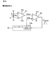
- FIG. 2 is a timing chart for explaining the delay of zero detection of the inductor current iL in the current detection circuit in the conventional example.
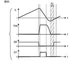
- Td in FIG. 2 shows the delay time of zero detection due to the delay by the operational amplifier and the noise filter. That is, due to the delay of the comparator IC and the time constant of the noise filter, the comparator starts up with a delay from the ideal current zero detection point, so that the negative current increases as shown in FIG.
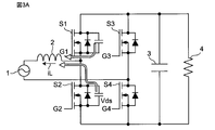
- FIG. 3A is a circuit diagram of a switching power supply device for explaining the mechanism by which the loss of the switching power supply device increases due to the delay of zero detection of the inductor current
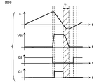
- FIG. 3B is a timing chart showing the operation of the switching power supply device of FIG. 3A.
- the switching power supply device includes an AC power supply 1, an inductor 2, switching elements S1 to S4, a smoothing capacitor 3, and a load resistor 4.
- FIG. 3B shows an inductor current iL, a drain-source voltage Vds of the switching element S2, a drive signal G2 for the switching element S2, and a drive signal G1 for the switching element S1.
- T1 indicates a period during which soft switching is performed by the negative current of the inductor current iL.
- An object of the present invention is to solve the above problems, and in a PFC circuit operating in a current critical mode, a control circuit of a power converter capable of accurately detecting the zero point of the inductor current as compared with the prior art. And to provide the power conversion device.
- the control circuit of the power conversion device is A control circuit for a power converter that includes an inductor and a PFC circuit that operates in current critical mode.
- a first unit that detects the current of the inductor or the current corresponding to the current of the inductor or includes the current of the inductor, amplifies the voltage corresponding to the detected current with a predetermined gain, and then outputs the voltage as the detection voltage.
- a comparator that compares the detected voltage with a predetermined reference voltage and outputs a comparison result signal
- a second detection circuit that detects the input voltage of the power converter, and It is provided with a third detection circuit that detects the output voltage of the power converter.
- the control circuit has the detected input voltage, the detected output voltage V, a preset delay time, an inductance value of the inductor, and a conversion coefficient when converting a current detected by the first detection circuit into a voltage. Based on the power supply voltage and the gain of the gain, the reference voltage for detecting the zero value of the current of the inductor is calculated and output to the comparator. And.
- the present invention in the PFC circuit operating in the current critical mode, it is possible to prevent the detection delay of the inductor current and accurately detect the zero point of the inductor current as compared with the prior art. This reduces the loss of the power converter and leads to a higher density of the power supply device.
- FIG. 1A is a circuit diagram showing a configuration example of a switching power supply device including the control circuit 20 according to the embodiment.
- the switching power supply device includes an AC power supply 1, a reactor 2 inductor, bridge-connected switching elements S1 to S4, a smoothing capacitor 3, a load resistor 4, and a shunt resistor. It includes Rs and a control circuit 20.
- the control circuit 20 includes a controller 10, a current detection unit 5, a drive signal generation circuit 11, an input voltage detection circuit 12, and an output voltage detection circuit 13.
- the input voltage Vin generated by the AC power supply 1 is input to the bridge connection circuit of the switching elements S1 to S4 via the shunt resistor Rs and the inductor 2.
- the switching elements S1 to S4 are turned on / off by the drive signals G1 to G4 from the drive signal generation circuit 11, and after the input voltage Vin is switched, the smoothed direct current is passed through the smoothing capacitor 3.
- the voltage is output to the load resistor 4 as the output voltage Vout.
- the shunt resistor Rs converts the inductor current iL into a voltage value and outputs it to the current detection unit 5.
- the input voltage detection circuit 12 detects the input voltage Vin and outputs it to the controller 10, and the output voltage detection circuit 13 detects the output voltage Vout and outputs it to the controller 10.
- the controller 10 controls the drive signal generation circuit 11 so as to generate the drive signals G1 to G4 in the current critical mode, for example, based on each input signal.
- the controller 10 includes a DA converter 10a that generates a reference voltage Vref determined in advance by a method described in detail later.
- FIG. 1B is a circuit diagram showing a configuration example of the current detection unit 5 of FIG. 1A.
- the current detection unit 5 includes an operational amplifier 21 and a comparator 22.
- Vcc is the power supply voltage.
- the operational amplifier 21 amplifies the voltage corresponding to the inductor current iL detected by the shunt resistor Rs, and outputs the amplified voltage Vamp to the comparator 22.
- the comparator 22 compares the input amplification voltage Vamp with the reference voltage Vref from the DA converter 10a in the controller 10, generates a comparison result voltage Vcomp, and outputs the comparison result voltage Vcomp to the controller 10.
- the controller 10 detects the zero current of the inductor current iL based on the comparison result voltage Vcomp, and based on this, for example, performs a switching operation in the current critical mode to generate drive signals G1 to G4.
- the drive signal generation circuit 11 is controlled so as to generate the current.
- the polarity of the reference voltage Vref is inverted according to the input voltage Vin (FIG. 1A) to the PFC circuit, that is, according to the direction of the inductor current iL.
- the detection delay can be prevented by changing the reference voltage Vref of the comparator 22 according to the delay time.
- Vref the reference voltage
- FIG. 4A is a circuit diagram showing a configuration example of the current detection unit according to the conventional example
- FIG. 4B is a timing chart showing the operation of the current detection unit of FIG. 4A.
- the reference voltage Vref of the comparator 22 is a constant voltage such as Vcc / 2
- a delay time Tdelay occurs as shown in FIG. 4B.
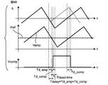
- FIG. 4C is a circuit diagram showing a configuration example of the current detection unit 5 according to the embodiment
- FIG. 4D is a timing chart showing the operation of the current detection unit 5 of FIG. 4C.
- the reference voltage Vref is raised from the DA converter 10a of the controller 10 according to the delay time. That is, in a PFC circuit in which the input voltage is alternating current, the delay time Tdelay can be reduced by changing the reference voltage Vref depending on the input voltage Vin, as shown in FIG. 4D, as compared with FIG. 4B. it can.
- Td_amp is the delay time due to the amplification operation of the operational amplifier 21.
- Td_comp is the delay time due to the comparison operation of the comparator 22.
- Tdead-time is the dead time of the switching elements S1 and S2.
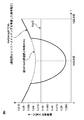
- FIG. 5 is a graph showing the operation of the current detection unit 5 according to the embodiment.
- Vref half cycle of the input voltage Vin
- Tdelay 50ns
- Vin (rms) 200V
- f LINE 50Hz
- FIG. 6 is a block diagram showing a configuration example of a power conversion device using the PFC circuit according to the embodiment.
- the power conversion device includes an AC power supply 1, a PFC circuit 100, a DC / DC converter 101, and a load 102. Since the control target is a PFC circuit, the input AC voltage and the output DC voltage are Vin (t) and Vout, respectively.
- the input voltage Vin is expressed by the following equation.
- the resistance value of the shunt resistor Rs is Rs
- the gain of the operational amplifier 21 is G
- the voltage applied to the operational amplifier 21 and the comparator 22 is Vcc.
- FIG. 7 is a waveform diagram for explaining a method of deriving the reference voltage Vref used in the current detection unit 5 according to the embodiment.
- the inductor current iL in the half cycle of the input voltage Vin is as shown in the graph of FIG. 7, and an enlarged view of one switching cycle is shown on the right side.
- the slope of the inductor current iL is obtained from win (t), Vout, and the inductance value L.
- the current fluctuation amount ⁇ idelay that changes during the delay time is expressed by the following equation.
- FIG. 8A and 8B are waveform diagrams for explaining soft switching of the PFC circuit by the current detection unit 5 according to the embodiment.
- FIG. 8A is a waveform diagram when Vin> Vout / 2
- FIG. 8B is a waveform diagram when additional on-time control is performed.
- the present embodiment is characterized in that TCM control is performed only by changing the reference voltage Vref of the comparator 22 by using a known TCM (Triangular Current Mode) control method.
- TCM Triangular Current Mode
- Vin Input voltage
- Vds Drain-source voltage of main switch element
- iL Inductor current
- Vgs Gate-source voltage of main switch element
- the controller 10 detects the detected input voltage Vin and output voltage Vout, the preset delay time, the inductance value of the inductor 2, and the resistance value of the shunt resistance Rs (in the modification described later, when the current is detected). It is a conversion coefficient when converting the inductor current iL into a voltage, and is generally the conversion coefficient.)
- the reference voltage Vref for making the delay of is substantially zero is calculated and output to the comparator 22.
- the synchronous rectifier switch element is kept on for a predetermined additional time ⁇ [ns] from the current zero detection point to flow a negative current for extracting the electric charge.
- the soft switching method shown in FIGS. 8A and 8B allows a negative current required for soft switching to flow by continuously turning on + ⁇ [ns] and giving an additional on time.
- the negative current required for soft switching can be adjusted to flow by changing the reference voltage Vref.
- FIG. 9 is a waveform diagram for explaining a method of deriving the reference voltage Vref used in the current detection unit 5 according to the modified example.
- the reference voltage Vref only for the delay prevention control of FIG. 5 is lowered for a predetermined time period, for example, in an elliptical shape.
- the negative current required for soft switching can be obtained from the input voltage Vin, the output voltage Vout, and the inductor tans L of the inductor 2, and can be realized by adding it to the reference voltage Vref in consideration of the delay time.
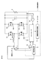
- FIG. 10A is a block diagram showing a configuration example of the switching power supply device according to the first modification.
- the inductor current iL flowing through the shunt resistor Rs is detected, but the present invention is not limited to this, and as shown in FIG. 10A, for example, CT (Current Transformer), Hall element, GMR (Giant Magneto). Resistive effect)
- CT Current Transformer
- Hall element Hall element
- GMR Giant Magneto
- Resistive effect The inductor current iL may be detected by using a current sensor 14 such as an element.
- FIG. 10B is a block diagram showing a configuration example of the switching power supply device according to the second modification.
- a shunt resistor Rs1 may be inserted between the ground side of the switching elements S2 and S4 and the load resistor 4, and the zero point of the inductor current iL may be detected.
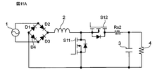
- FIG. 11A is a block diagram showing a configuration example of the switching power supply device according to the third modification.
- FIG. 11A shows an example of a synchronous rectification type step-up PFC circuit.
- the switching power supply device includes an AC power supply 1, four bridge-connected diodes D1 to D4, a reactor inductor 2, switching elements S11 and S12, a shunt resistor Rs2, and a smoothing capacitor 3.
- a load resistor 4 is provided.
- a shunt resistor Rs2 for detecting the zero point of the inductor current iL is inserted between the switching element S12 and the smoothing capacitor 3. It is preferable to do so.
- FIG. 11B is a block diagram showing a configuration example of the switching power supply device according to the modified example 4.
- a shunt resistor Rs3 for detecting the zero point of the inductor current iL may be inserted between the diodes D1 and D4 and the inductor 2.
- the current corresponding to the inductor current iL or the current including the inductor current iL is detected.
- FIG. 12 is a circuit diagram showing a modified example of the current detection unit 5 of FIG. 1B.
- a controller 10A having a DA converter 10a, a comparator 22 and a signal processing unit 10b is provided.
- the signal processing unit 10b performs signal processing for changing the above-mentioned reference voltage Vref based on the comparison result signal Vcomp from the comparator 22.
- Some controllers such as DSPs (digital signal processors) have a built-in comparator function as well as AD converters and DA converters. By using the built-in comparator 22, there is an advantage that an external comparator IC becomes unnecessary.
- the inductor current detection delay is prevented and the inductor is more accurately compared with the prior art.
- the zero point of the current can be detected accurately. This reduces the loss of the power converter and leads to a higher density of the power supply device. In particular, since no magnetic material is used, the loss does not increase even when driven at high frequencies, and no additional parts are required. Further, by applying the method of changing the reference voltage Vref, a soft switching function using voltage resonance can be easily implemented.
- switching power supply device is described in the above embodiments or modifications, the present invention is not limited to this, and can be applied to various power conversion devices including the switching power supply device.
- the detection delay of the inductor current is prevented, and the zero point of the inductor current is accurately detected as compared with the prior art. can do. This reduces the loss of the power converter and leads to a higher density of the power supply device.
Landscapes
- Engineering & Computer Science (AREA)
- Power Engineering (AREA)
- Rectifiers (AREA)
- Dc-Dc Converters (AREA)
Priority Applications (5)
| Application Number | Priority Date | Filing Date | Title |
|---|---|---|---|
| JP2021539708A JP7160208B2 (ja) | 2019-08-09 | 2019-08-09 | 電力変換装置の制御回路 |
| CN201980098644.XA CN114144969B (zh) | 2019-08-09 | 2019-08-09 | 电力转换装置的控制电路 |
| US17/628,692 US12021448B2 (en) | 2019-08-09 | 2019-08-09 | Control circuit for power converter apparatus provided with PFC circuit operating in current critical mode |
| EP19941248.7A EP4012912B1 (en) | 2019-08-09 | 2019-08-09 | Control circuit for power conversion device |
| PCT/JP2019/031654 WO2021028972A1 (ja) | 2019-08-09 | 2019-08-09 | 電力変換装置の制御回路 |
Applications Claiming Priority (1)
| Application Number | Priority Date | Filing Date | Title |
|---|---|---|---|
| PCT/JP2019/031654 WO2021028972A1 (ja) | 2019-08-09 | 2019-08-09 | 電力変換装置の制御回路 |
Publications (1)
| Publication Number | Publication Date |
|---|---|
| WO2021028972A1 true WO2021028972A1 (ja) | 2021-02-18 |
Family
ID=74570603
Family Applications (1)
| Application Number | Title | Priority Date | Filing Date |
|---|---|---|---|
| PCT/JP2019/031654 Ceased WO2021028972A1 (ja) | 2019-08-09 | 2019-08-09 | 電力変換装置の制御回路 |
Country Status (5)
| Country | Link |
|---|---|
| US (1) | US12021448B2 (https=) |
| EP (1) | EP4012912B1 (https=) |
| JP (1) | JP7160208B2 (https=) |
| CN (1) | CN114144969B (https=) |
| WO (1) | WO2021028972A1 (https=) |
Families Citing this family (3)
| Publication number | Priority date | Publication date | Assignee | Title |
|---|---|---|---|---|
| US11764668B2 (en) * | 2018-12-06 | 2023-09-19 | Rohm Co., Ltd. | Control device for controlling an electric power conversion device incorporating a bidirectional inverter |
| CN115085531A (zh) * | 2022-07-05 | 2022-09-20 | 华为数字能源技术有限公司 | 一种图腾柱pfc电路的控制方法、装置和电子设备 |
| CN116015046B (zh) * | 2022-12-30 | 2025-11-18 | 超聚变数字技术有限公司 | 一种开关电源及计算设备 |
Citations (2)
| Publication number | Priority date | Publication date | Assignee | Title |
|---|---|---|---|---|
| WO2011030640A1 (ja) * | 2009-09-11 | 2011-03-17 | 株式会社村田製作所 | Pfcコンバータ |
| US20130194842A1 (en) * | 2012-01-26 | 2013-08-01 | Stmicroelectronics S.R.L. | Control device of a switching power supply |
Family Cites Families (10)
| Publication number | Priority date | Publication date | Assignee | Title |
|---|---|---|---|---|
| KR101026248B1 (ko) | 2004-09-21 | 2011-03-31 | 페어차일드코리아반도체 주식회사 | 역률 보상 회로 |
| CN101552546B (zh) * | 2008-04-02 | 2011-10-12 | 台达能源技术(上海)有限公司 | 用于临界导通模式的无桥功率因数校正电路及其控制方法 |
| US8379420B2 (en) * | 2010-10-13 | 2013-02-19 | Power Integrations, Inc. | Controller with punctuated switching control circuit |
| JP6024201B2 (ja) * | 2012-05-21 | 2016-11-09 | 富士電機株式会社 | スイッチング電源装置 |
| CN104620483B (zh) * | 2012-05-31 | 2017-05-31 | 松下电器产业株式会社 | 电力转换电路的控制装置 |
| CN203465347U (zh) * | 2013-09-02 | 2014-03-05 | 南京埃科孚电子科技有限公司 | 用于升压型功率因数校正的电感电流过零检测电路 |
| CN103675426B (zh) * | 2013-12-24 | 2017-04-26 | 矽力杰半导体技术(杭州)有限公司 | 电感电流过零检测方法及电路以及带该电路的开关电源 |
| CN104009620A (zh) * | 2014-06-16 | 2014-08-27 | 南京航空航天大学 | 逆变器的控制型软开关技术 |
| US10090757B2 (en) * | 2016-08-19 | 2018-10-02 | Fairchild Semiconductor Corporation | Power factor correction circuit and method |
| US11005361B2 (en) * | 2019-06-19 | 2021-05-11 | Stmicroelectronics S.R.L. | Control circuit and method of a switching power supply |
-
2019
- 2019-08-09 JP JP2021539708A patent/JP7160208B2/ja active Active
- 2019-08-09 WO PCT/JP2019/031654 patent/WO2021028972A1/ja not_active Ceased
- 2019-08-09 US US17/628,692 patent/US12021448B2/en active Active
- 2019-08-09 EP EP19941248.7A patent/EP4012912B1/en active Active
- 2019-08-09 CN CN201980098644.XA patent/CN114144969B/zh active Active
Patent Citations (2)
| Publication number | Priority date | Publication date | Assignee | Title |
|---|---|---|---|---|
| WO2011030640A1 (ja) * | 2009-09-11 | 2011-03-17 | 株式会社村田製作所 | Pfcコンバータ |
| US20130194842A1 (en) * | 2012-01-26 | 2013-08-01 | Stmicroelectronics S.R.L. | Control device of a switching power supply |
Non-Patent Citations (1)
| Title |
|---|
| QINGYUN HUANG ET AL.: "Predictive ZVS Control with Improved ZVS Time Margin and Limited Variable Frequency Range for A 99% Efficient, 130W/in3 MHz GaN Totem-Pole PFC Rectifier", IEEE TRANSACTIONS ON POWER ELECTRONICS, vol. 34, no. 7, 2018 |
Also Published As
| Publication number | Publication date |
|---|---|
| CN114144969A (zh) | 2022-03-04 |
| US20220271650A1 (en) | 2022-08-25 |
| JPWO2021028972A1 (https=) | 2021-02-18 |
| EP4012912A4 (en) | 2023-04-12 |
| US12021448B2 (en) | 2024-06-25 |
| EP4012912A1 (en) | 2022-06-15 |
| JP7160208B2 (ja) | 2022-10-25 |
| EP4012912B1 (en) | 2024-05-22 |
| CN114144969B (zh) | 2024-11-12 |
Similar Documents
| Publication | Publication Date | Title |
|---|---|---|
| JP7293968B2 (ja) | 電力変換装置の制御回路及び電力変換装置 | |
| JP3994953B2 (ja) | 力率改善回路 | |
| JP5182375B2 (ja) | Pfcコンバータ | |
| JP6859034B2 (ja) | 共振変換器における同期整流のための回路および方法 | |
| KR20200040673A (ko) | Pfc 버스트 모드 제어 기능이 있는 스위치 모드 전원 공급 장치 | |
| TWI565204B (zh) | Dynamic detection regulator boost power factor correction control device | |
| CN108233696B (zh) | 控制脉冲宽度调制开关频率的装置和方法 | |
| US9923455B2 (en) | Current-sensing and gain-switching circuit and method for using wide range of current | |
| KR20170080518A (ko) | 역률 보상 회로 및 역률 보상 회로의 구동 방법 | |
| JP6147209B2 (ja) | 電力変換装置 | |
| CN114070034B (zh) | 电力转换装置 | |
| JP2014042433A (ja) | 平均電流モード制御によるブリッジレスpfcコンバータ | |
| JP7160208B2 (ja) | 電力変換装置の制御回路 | |
| CN107078655A (zh) | 电力转换装置 | |
| EP2793382A2 (en) | Power transforming apparatus | |
| JP2011166903A (ja) | スイッチング電源装置 | |
| JP5933418B2 (ja) | 電力変換装置 | |
| JPWO2021028972A5 (https=) | ||
| JP2014147224A (ja) | スイッチングレギュレータ | |
| JP4423994B2 (ja) | 力率改善回路 | |
| KR101905345B1 (ko) | 전력 변환 장치 | |
| CN121173088A (zh) | 图腾柱功率因数校正电路中的电流检测 | |
| CN117394554A (zh) | 无线充电系统及其控制方法和控制装置、电子设备 | |
| TW201929403A (zh) | 具電流估測電路之直流-直流轉換器電路架構 | |
| CN106300954A (zh) | 动态侦测稳压升压功率因数校正控制装置 |
Legal Events
| Date | Code | Title | Description |
|---|---|---|---|
| 121 | Ep: the epo has been informed by wipo that ep was designated in this application |
Ref document number: 19941248 Country of ref document: EP Kind code of ref document: A1 |
|
| ENP | Entry into the national phase |
Ref document number: 2021539708 Country of ref document: JP Kind code of ref document: A |
|
| NENP | Non-entry into the national phase |
Ref country code: DE |
|
| ENP | Entry into the national phase |
Ref document number: 2019941248 Country of ref document: EP Effective date: 20220309 |