WO2021025120A1 - 照明装置 - Google Patents
照明装置 Download PDFInfo
- Publication number
- WO2021025120A1 WO2021025120A1 PCT/JP2020/030205 JP2020030205W WO2021025120A1 WO 2021025120 A1 WO2021025120 A1 WO 2021025120A1 JP 2020030205 W JP2020030205 W JP 2020030205W WO 2021025120 A1 WO2021025120 A1 WO 2021025120A1
- Authority
- WO
- WIPO (PCT)
- Prior art keywords
- light emitting
- light
- peak wavelength
- wavelength
- emitting device
- Prior art date
- Legal status (The legal status is an assumption and is not a legal conclusion. Google has not performed a legal analysis and makes no representation as to the accuracy of the status listed.)
- Ceased
Links
Images





Classifications
-
- H—ELECTRICITY
- H10—SEMICONDUCTOR DEVICES; ELECTRIC SOLID-STATE DEVICES NOT OTHERWISE PROVIDED FOR
- H10W—GENERIC PACKAGES, INTERCONNECTIONS, CONNECTORS OR OTHER CONSTRUCTIONAL DETAILS OF DEVICES COVERED BY CLASS H10
- H10W90/00—Package configurations
-
- F—MECHANICAL ENGINEERING; LIGHTING; HEATING; WEAPONS; BLASTING
- F21—LIGHTING
- F21S—NON-PORTABLE LIGHTING DEVICES; SYSTEMS THEREOF; VEHICLE LIGHTING DEVICES SPECIALLY ADAPTED FOR VEHICLE EXTERIORS
- F21S2/00—Systems of lighting devices, not provided for in main groups F21S4/00 - F21S10/00 or F21S19/00, e.g. of modular construction
-
- F—MECHANICAL ENGINEERING; LIGHTING; HEATING; WEAPONS; BLASTING
- F21—LIGHTING
- F21V—FUNCTIONAL FEATURES OR DETAILS OF LIGHTING DEVICES OR SYSTEMS THEREOF; STRUCTURAL COMBINATIONS OF LIGHTING DEVICES WITH OTHER ARTICLES, NOT OTHERWISE PROVIDED FOR
- F21V9/00—Elements for modifying spectral properties, polarisation or intensity of the light emitted, e.g. filters
- F21V9/30—Elements containing photoluminescent material distinct from or spaced from the light source
- F21V9/32—Elements containing photoluminescent material distinct from or spaced from the light source characterised by the arrangement of the photoluminescent material
-
- F—MECHANICAL ENGINEERING; LIGHTING; HEATING; WEAPONS; BLASTING
- F21—LIGHTING
- F21S—NON-PORTABLE LIGHTING DEVICES; SYSTEMS THEREOF; VEHICLE LIGHTING DEVICES SPECIALLY ADAPTED FOR VEHICLE EXTERIORS
- F21S4/00—Lighting devices or systems using a string or strip of light sources
- F21S4/20—Lighting devices or systems using a string or strip of light sources with light sources held by or within elongate supports
-
- F—MECHANICAL ENGINEERING; LIGHTING; HEATING; WEAPONS; BLASTING
- F21—LIGHTING
- F21V—FUNCTIONAL FEATURES OR DETAILS OF LIGHTING DEVICES OR SYSTEMS THEREOF; STRUCTURAL COMBINATIONS OF LIGHTING DEVICES WITH OTHER ARTICLES, NOT OTHERWISE PROVIDED FOR
- F21V23/00—Arrangement of electric circuit elements in or on lighting devices
- F21V23/003—Arrangement of electric circuit elements in or on lighting devices the elements being electronics drivers or controllers for operating the light source, e.g. for a LED array
-
- F—MECHANICAL ENGINEERING; LIGHTING; HEATING; WEAPONS; BLASTING
- F21—LIGHTING
- F21V—FUNCTIONAL FEATURES OR DETAILS OF LIGHTING DEVICES OR SYSTEMS THEREOF; STRUCTURAL COMBINATIONS OF LIGHTING DEVICES WITH OTHER ARTICLES, NOT OTHERWISE PROVIDED FOR
- F21V9/00—Elements for modifying spectral properties, polarisation or intensity of the light emitted, e.g. filters
- F21V9/30—Elements containing photoluminescent material distinct from or spaced from the light source
-
- H—ELECTRICITY
- H05—ELECTRIC TECHNIQUES NOT OTHERWISE PROVIDED FOR
- H05B—ELECTRIC HEATING; ELECTRIC LIGHT SOURCES NOT OTHERWISE PROVIDED FOR; CIRCUIT ARRANGEMENTS FOR ELECTRIC LIGHT SOURCES, IN GENERAL
- H05B45/00—Circuit arrangements for operating light-emitting diodes [LED]
- H05B45/10—Controlling the intensity of the light
-
- F—MECHANICAL ENGINEERING; LIGHTING; HEATING; WEAPONS; BLASTING
- F21—LIGHTING
- F21Y—INDEXING SCHEME ASSOCIATED WITH SUBCLASSES F21K, F21L, F21S and F21V, RELATING TO THE FORM OR THE KIND OF THE LIGHT SOURCES OR OF THE COLOUR OF THE LIGHT EMITTED
- F21Y2103/00—Elongate light sources, e.g. fluorescent tubes
- F21Y2103/10—Elongate light sources, e.g. fluorescent tubes comprising a linear array of point-like light-generating elements
-
- F—MECHANICAL ENGINEERING; LIGHTING; HEATING; WEAPONS; BLASTING
- F21—LIGHTING
- F21Y—INDEXING SCHEME ASSOCIATED WITH SUBCLASSES F21K, F21L, F21S and F21V, RELATING TO THE FORM OR THE KIND OF THE LIGHT SOURCES OR OF THE COLOUR OF THE LIGHT EMITTED
- F21Y2115/00—Light-generating elements of semiconductor light sources
- F21Y2115/10—Light-emitting diodes [LED]
-
- H—ELECTRICITY
- H05—ELECTRIC TECHNIQUES NOT OTHERWISE PROVIDED FOR
- H05B—ELECTRIC HEATING; ELECTRIC LIGHT SOURCES NOT OTHERWISE PROVIDED FOR; CIRCUIT ARRANGEMENTS FOR ELECTRIC LIGHT SOURCES, IN GENERAL
- H05B45/00—Circuit arrangements for operating light-emitting diodes [LED]
- H05B45/20—Controlling the colour of the light
-
- H—ELECTRICITY
- H10—SEMICONDUCTOR DEVICES; ELECTRIC SOLID-STATE DEVICES NOT OTHERWISE PROVIDED FOR
- H10H—INORGANIC LIGHT-EMITTING SEMICONDUCTOR DEVICES HAVING POTENTIAL BARRIERS
- H10H20/00—Individual inorganic light-emitting semiconductor devices having potential barriers, e.g. light-emitting diodes [LED]
- H10H20/80—Constructional details
- H10H20/85—Packages
- H10H20/851—Wavelength conversion means
Definitions
- This disclosure relates to lighting equipment.
- a lighting device using semiconductor light emitting elements such as LEDs (Light Emitting Diodes) as light sources have been used. Further, for example, a lighting device using a light emitting element as a light source is also used as a light source for visual inspection of a painted surface of home appliances and passenger automobiles.
- Semiconductor light emitting devices have a narrow wavelength band of synchrotron radiation and can only emit light of a single color.
- a plurality of semiconductor light emitting elements having different wavelength bands of synchrotron radiation are prepared, and white light is realized by mixing the colors of the plurality of synchrotron radiation.
- a plurality of phosphors that emit fluorescence having different wavelength bands by excitation light of the same wavelength are prepared, and the emission light from the semiconductor light emitting element and the plurality of fluorescence excited by the radiation light from the semiconductor light emitting element emit light.
- White light is realized by mixing colors. By using such a color mixing method, it is possible to produce a light source having a spectrum other than white light according to the purpose (see JP-A-2015-126160).
- Patent Document 1 has not been described or assumed at all up to the control of the emission intensity and the emission spectrum of the lighting device.
- the lighting device includes a first light emitting device, a plurality of second light emitting devices, and a control unit.
- the first light emitting device has a first peak wavelength in the wavelength region of 360 to 430 nm, and has a first light emitting spectrum in which the light intensity continuously decreases toward shorter wavelengths and longer wavelengths than the first peak wavelength, respectively.
- Each of the plurality of second light emitting devices has a second peak wavelength in a wavelength region of 360 to 430 nm, a third peak wavelength in a wavelength region from a wavelength longer than the second peak wavelength to 750 nm, and a second peak.
- Each has a second emission spectrum in which the light intensity continuously decreases toward a wavelength shorter than the wavelength and a wavelength longer than the third peak wavelength.
- the control unit controls the first light emitting device and the plurality of second light emitting devices.
- the plurality of second light emitting devices have different third peak wavelengths.
- the lighting apparatus has an emission peak wavelength in the wavelength region of 360 nm to 430 nm and an emission peak wavelength in the wavelength region of 610 nm to 730 nm. Further, in the emission spectrum, when the light intensity at the emission peak wavelength is 1, the relative light intensity at the excitation peak wavelength is 0.05 to 0.3, and the relative light intensity at 440 nm to 480 nm is 0.1. Below, the light intensity in the wavelength region from 480 nm to the emission peak wavelength is continuously increasing.
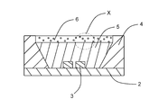
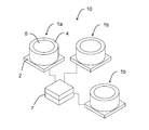
- FIG. 1 is an external perspective view of the light emitting device according to the embodiment of the present disclosure.
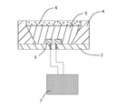
- FIG. 2 is a cross-sectional view of the light emitting device shown in FIG. 1 when it is cut along a plane shown by a virtual line.
- FIG. 12 is a block diagram of the lighting device according to the embodiment of the present disclosure.
- the lighting device 10 includes a first light emitting device 1a, a plurality of second light emitting devices 1b, and a control unit 7. Further, the first light emitting device 1a and the second light emitting device 1b include a substrate 2, a light emitting element 3, a frame body 4, and a sealing member 5.
- the lighting device 10 includes a first light emitting device 1a, a plurality of second light emitting devices 1b, and a control unit 7.
- the second light emitting device 1b includes a substrate 2, a light emitting element 3, a frame body 4, a sealing member 5, and a wavelength conversion member 6.
- the light emitting element 3 is located on the substrate 2.
- the frame body 4 is located on the substrate 2 so as to surround the light emitting element 3.
- the sealing member 5 is filled in the inner space surrounded by the frame body 4, leaving a part of the upper part of the space surrounded by the frame body 4.
- the wavelength conversion member 6 is housed in the frame 4 along the upper surface of the sealing member 5 in a part of the upper part of the inner space surrounded by the frame 4.
- the light emitting element 3 is, for example, an LED (Light Emitting Diode) or an LD (Laser Diode), and emits light toward the outside by recombination of electrons and holes during a pn junction using a semiconductor. discharge.
- the substrate 2 is a substrate mainly composed of an insulating material, and the insulating material is made of, for example, a ceramic material such as alumina or mullite, or a glass ceramic material. Alternatively, it is composed of a composite material in which a plurality of these materials are mixed. Further, as the substrate 2, a polymer resin in which metal oxide fine particles capable of adjusting the thermal expansion of the substrate 2 are dispersed can be used.
- a wiring conductor that electrically conducts the inside and outside of the substrate 2 is provided.
- the wiring conductor is made of a conductive material such as tungsten, molybdenum, manganese or copper.
- a metal paste obtained by adding an organic solvent to a powder such as tungsten is printed on a ceramic green sheet to be the substrate 2 in a predetermined pattern. After that, it is obtained by laminating a plurality of ceramic green sheets and firing them.
- a plating layer such as nickel or gold is formed on the surface of the wiring conductor to prevent oxidation.
- a metal reflective layer may be located on the upper surface of the substrate 2 at a distance from the wiring conductor and the plating layer.
- the metal reflective layer is, for example, aluminum, silver, gold, copper or platinum.
- the light emitting element 3 is mounted on the main surface of the substrate 2.
- the light emitting element 3 is electrically connected to the plating layer that adheres to the surface of the wiring conductor formed on the upper surface of the substrate 2 via, for example, a brazing material or solder.
- the light emitting element 3 has a translucent substrate and an optical semiconductor layer formed on the translucent substrate.
- the translucent substrate may be one capable of growing an optical semiconductor layer by using a chemical vapor deposition method such as an organic metal vapor phase growth method or a molecular beam epitaxial growth method.
- As the material used for the translucent substrate for example, sapphire, gallium nitride, aluminum nitride, zinc oxide, zinc selenide, silicon carbide, silicon, zirconium dibodium or the like can be used.
- the thickness of the translucent substrate is, for example, 50 ⁇ m or more and 1000 ⁇ m or less.
- the optical semiconductor layer is composed of a first semiconductor layer formed on a translucent substrate, a light emitting layer formed on the first semiconductor layer, and a second semiconductor layer formed on the light emitting layer. ..
- the first semiconductor layer, the light emitting layer and the second semiconductor layer are, for example, a group III nitride semiconductor, a group III-V semiconductor such as gallium phosphorus or gallium arsenide, or a group III nitride such as gallium nitride, aluminum nitride or indium nitride. Material semiconductors and the like can be used.
- the thickness of the first semiconductor layer is, for example, 1 ⁇ m or more and 5 ⁇ m or less
- the thickness of the light emitting layer is, for example, 25 nm or more and 150 nm or less
- the thickness of the second semiconductor layer is, for example, 50 nm or more and 600 nm or less.
- the light emitting element 3 configured in this way can emit excitation light in a wavelength region of, for example, 280 nm or more and 450 nm or less.
- the frame 4 is mixed with, for example, a ceramic material such as aluminum oxide, titanium oxide, zirconium oxide or yttrium oxide, or a porous material, or a powder made of a metal oxide such as aluminum oxide, titanium oxide, zirconium oxide or yttrium oxide. It consists of a resin material that has been made to.
- the frame body 4 is connected to the main surface of the substrate 2 via, for example, resin, brazing material, solder, or the like.
- the frame 4 is provided on the main surface of the substrate 2 so as to surround the light emitting element 3 at a distance from the light emitting element 3. Further, the frame body 4 is formed so that the inclined inner wall surface expands outward as the distance from the main surface of the substrate 2 increases.
- the inner wall surface of the frame body 4 functions as a reflecting surface of the excitation light emitted from the light emitting element 3.
- the shape of the inner wall surface of the frame body 4 is circular in a plan view, the light emitted by the light emitting element 3 can be uniformly reflected outward by the reflecting surface.
- the inclined inner wall surface of the frame body 4 is made of, for example, a metal layer made of tungsten, molybdenum, manganese or the like on the inner peripheral surface of the frame body 4 made of a sintered material, and nickel or gold or the like covering the metal layer.
- a plating layer may be formed. This plating layer has a function of reflecting the light emitted by the light emitting element 3.
- the inclination angle of the inner wall surface of the frame body 4 is set to, for example, 55 degrees or more and 70 degrees or less with respect to the main surface of the substrate 2.
- the inner space surrounded by the substrate 2 and the frame 4 is filled with a light-transmitting sealing member 5.
- the sealing member 5 seals the light emitting element 3 and takes out the light emitted from the inside of the light emitting element 3 to the outside. Further, it has a function of transmitting light taken out to the outside of the light emitting element 3.
- the sealing member 5 is filled in the inner space surrounded by the substrate 2 and the frame body 4, leaving a part of the space surrounded by the frame body 4.
- a translucent insulating resin such as a silicone resin, an acrylic resin or an epoxy resin, or a translucent glass material is used.
- the refractive index of the sealing member 5 is set to, for example, 1.4 or more and 1.6 or less.
- the wavelength conversion member 6 is located in the upper part of the inner space surrounded by the substrate 2 and the frame 4 along the upper surface of the sealing member 5.
- the wavelength conversion member 6 is formed so as to fit within the frame body 4.
- the wavelength conversion member 6 has a function of converting the wavelength of the light emitted by the light emitting element 3. That is, in the wavelength conversion member 6, the light emitted from the light emitting element 3 is incident on the inside through the sealing member 5. At that time, the phosphor contained inside is excited by the light emitted from the light emitting element 3 to emit fluorescence from the phosphor. Further, a part of the light from the light emitting element 3 is transmitted and emitted.
- the wavelength conversion member 6 is made of, for example, a translucent insulating resin such as a fluororesin, a silicone resin, an acrylic resin or an epoxy resin, or a translucent glass material, and a phosphor is contained in the insulating resin or the glass material. It is contained. The phosphor is uniformly dispersed in the wavelength conversion member 6. The phosphor contained in the light emitting element 3 and the wavelength conversion member 6 is selected so that the light emission spectrum of the light emitted from the light emitting device 1 becomes the light emission spectrum as shown in FIG.
- a translucent insulating resin such as a fluororesin, a silicone resin, an acrylic resin or an epoxy resin, or a translucent glass material
- a phosphor is contained in the insulating resin or the glass material. It is contained.
- the phosphor is uniformly dispersed in the wavelength conversion member 6.
- the phosphor contained in the light emitting element 3 and the wavelength conversion member 6 is selected so that the light emission spectrum of the light emitted from the light emitting
- a light emitting element 3 having a first peak wavelength ⁇ 1 of 360 to 430 nm is used in the first light emitting device 1a of the embodiment of the present disclosure.
- a light emitting element 3 that emits excitation light having a second peak wavelength ⁇ 2 of 360 to 430 nm is used in the second light emitting device 1b. That is, the second peak wavelength ⁇ 2 is the peak wavelength of the excitation light.
- the second light emitting device 1b may have a third peak wavelength ⁇ 3 in a wavelength region from a wavelength longer than the second peak wavelength ⁇ 2 to 750 nm by irradiating the phosphor with excitation light, for example.
- the third peak wavelength ⁇ 3 is emitted in the wavelength region of 410 to 750 nm.
- the plurality of second light emitting devices 1b use phosphors that are at least partially different from each other. Further, a phosphor that emits blue fluorescence, a phosphor that emits bluish green fluorescence, a phosphor that emits green fluorescence, a phosphor that emits red fluorescence, and a phosphor that emits fluorescence in the near infrared region. You may use it. Further, it may be a mixture of these phosphors.
- the fluorescent substances showing blue color are BaMgAl 10 O 17 : Eu, (Sr, Ca, Ba) 10 (PO 4 ) 6 Cl 2 : Eu, (Sr, Ba) 10 (PO 4 ) 6 Cl. 2 :
- the phosphors that are Eu and show a bluish green color are (Sr, Ba, Ca) 5 (PO 4 ) 3 Cl: Eu, Sr 4 Al 14 O 25 : Eu.
- the phosphors showing green color are SrSi 2 (O, Cl) 2 N 2 : Eu, (Sr, Ba, Mg) 2 SiO 4 : Eu 2+ , ZnS: Cu, Al, Zn 2 SiO 4 : Mn.
- red phosphors examples include Y 2 O 2 S: Eu, Y 2 O 3 : Eu, SrCaClAlSiN 3 : Eu 2+ , CaAlSiN 3 : Eu, and CaAlSi (ON) 3 : Eu.
- the phosphor exhibiting the near infrared region is 3Ga 5 O 12 : Cr.
- the lighting device 10 includes the first light emitting device 1a, the second light emitting device 1b, and the control unit 7 described above.
- the emission spectrum of the light emitted from the first light emitting device 1a is defined as the first emission spectrum
- the emission spectrum of the light emitted from the second light emitting device 1b is defined as the second emission spectrum.
- the control unit 7 controls the first light emitting device 1a and the second light emitting device 1b.
- the emission spectrum of the light obtained by combining the first emission spectrum and the second emission spectrum controlled by the control unit 7, that is, the emission spectrum of the light emitted from the illuminating device 10 is defined as the third emission spectrum.
- the control unit 7 controls the dimming rate applied to each light emitting device.
- the dimming rate refers to the power applied to each light emitting device, that is, the voltage value and / or the current value ratio when the rated current value and / or the rated voltage value is used as a reference. Further, in the case of a configuration using PWM control, it refers to the detail ratio of voltage and / or current. As a result, the luminous flux output by each light emitting device can be adjusted.
- the control unit 7 can adjust the emission intensity of light emitted from the first light emitting device 1a and / or the second light emitting device 1b.
- the emission intensity is the illuminance of the light incident on the photosensitive surface, that is, the incident luminous flux per unit area.
- the light emission intensity of each light emitting device can be adjusted to an arbitrary value between 0 and 1 when the maximum light intensity is 1.
- light of various colors can be emitted by adjusting the ratio of the intensity of the light emitted from each light emitting device by adjusting every 0.1, adjusting every 0.01, and the like.
- the lighting device 10 has a first light emitting device 1a and a second light emitting device 1b having a second peak wavelength ⁇ 2, as shown in FIG. 12, which light emitting device is to be emitted and which light emitting device is used. It is also possible to adjust whether to increase the emission intensity. That is, the third emission spectrum of the illumination device 10 is a first emission spectrum which is a spectrum of light emitted from the first light emitting device 1a and a second emission spectrum which is a spectrum of light emitted from the second light emitting device 1b. It is a combination of and.
- the intensity of the first emission spectrum can be adjusted by adjusting the voltage or current applied to the first light emitting device 1a, and the intensity of the second emission spectrum can be adjusted by adjusting the voltage or current applied to the second light emitting device 1b. Can be adjusted.
- the emission spectrum of the light controlled in this way and emitted from the lighting device 10 is the third emission spectrum.
- the control unit 7 also adjusts which light emitting device is selected.
- control unit 7 selects the first light emitting device 1a as the light emitting device to emit light, and also controls which of the plurality of second light emitting devices 1b is to emit light based on the first light emitting spectrum. it can. Further, the control unit 7 selects a light emitting device as a reference for controlling the dimming rate from the first light emitting device 1a and the plurality of second light emitting devices 1b, and based on the dimming rate of the reference light emitting device. It is also possible to control the dimming rate of each light emitting device.
- the control unit 7 may set the first dimming rate of the first light emitting device 1a and control the dimming rate of each of the plurality of second light emitting devices 1b based on the first dimming rate. .. Further, the control unit 7 selects the second light emitting device 1b having the peak wavelength having the maximum light intensity in the wavelength region from a wavelength longer than the second peak wavelength ⁇ 2 to 750 nm from the plurality of second light emitting devices 1b. Then, the second dimming rate of the second light emitting device 1b is set. Then, the dimming rate of each of the first light emitting device 1a and the other plurality of second light emitting devices 1b may be controlled based on the second dimming rate.
- control unit 7 may control the first light emitting device 1a and / or the second light emitting device 1b described above based on a signal or information received wirelessly from the outside.
- the control unit 7 may include an arithmetic unit such as a CPU, a memory, and the like.
- the lighting device 10 includes a first light emitting device 1a, a plurality of second light emitting devices 1b, and a control unit 7.
- the first light emitting device 1a has a first peak wavelength ⁇ 1 in a wavelength region of 360 to 430 nm, and continuously has a light intensity in the range of 360 to 750 nm as the wavelength becomes shorter and longer than the first peak wavelength, respectively.
- Each of the plurality of second light emitting devices 1b has a second peak wavelength ⁇ 2 in a wavelength region of 360 to 430 nm, and has a third peak in a wavelength region up to 750 nm and on a longer wavelength side than the second peak wavelength ⁇ 2. It has a wavelength ⁇ 3 and has a second emission spectrum in which the light intensity continuously decreases toward a shorter wavelength than the second peak wavelength ⁇ 2 and a longer wavelength than the third peak wavelength ⁇ 3.
- the lighting device 10 has a plurality of second light emitting devices 1b.
- the third peak wavelength ⁇ 3 of each of the plurality of second light emitting devices 1b is preferably different wavelengths in a wavelength region of at least 430 nm to 750 nm.
- control unit 7 can select a light emitting device to emit light from the first light emitting device 1a and the plurality of second light emitting devices 1b. Further, the control unit 7 can also control the dimming rate of each of the first light emitting device 1a and the plurality of second light emitting devices 1b. That is, the control unit 7 can control the third emission spectrum of the lighting device 10 by controlling from which light emitting device the light emitting device emits light and at what brightness the light emitting device emits light. This makes it possible to control each light emitting device having spectra having different peak wavelengths. Therefore, the third emission spectrum can be changed according to various uses.
- the third peak wavelength ⁇ 3 of each of the plurality of second light emitting devices 1b is a different wavelength, and the half width at each third peak wavelength ⁇ 3 of the plurality of second light emitting devices 1b becomes larger toward a longer wavelength. It may be. When reproducing visible light such as the sunlight spectrum, it is necessary to reproduce even a longer wavelength region. Therefore, the half-value width becomes larger toward a longer wavelength, so that dimming becomes easier.
- the third peak wavelengths ⁇ 3 of the plurality of second light emitting devices 1b may be separated from each other by at least 10 nm or more. In an illuminating device having emission spectra having different peak wavelengths, the smaller the wavelength region in which the emission spectra overlap, the wider the wavelength region can be emitted.
- the light intensity at the second peak wavelength ⁇ 2 corresponding to the second light emitting device 1b is the first. It may be 25% or less of the light intensity at one peak wavelength ⁇ 1. That is, when the dimming rate of the first light emitting device 1a and the dimming rate of the second light emitting device 1b are the same, the light intensity at 360 to 430 nm may be the largest in the first light emitting device 1a.
- the third emission spectrum may have peak wavelengths at the positions of the first peak wavelength ⁇ 1, the second peak wavelength ⁇ 2, and the plurality of third peak wavelengths ⁇ 3. Since the emission spectrum of the illumination device 10 is an emission spectrum based on the combined light of the light emitted from the first light emitting device 1a and the plurality of second light emitting devices 1b, the light intensity is large depending on the dimming rate of each light emitting device. The light changes. At this time, the farther the third peak wavelengths ⁇ 3 of the plurality of second light emitting devices 1b are, the smaller the overlap of the light of the respective peak wavelengths is, and the more the peak positions are independent.
- the third emission spectrum of the light emitted as the illumination device 10 has a peak wavelength at the same wavelength as the third peak wavelength ⁇ 3 in each of the plurality of second light emitting devices 1b.
- the light intensity at the wavelength of the overlapping boundary is the higher of the target third peak wavelengths ⁇ 3.
- the peak of the third light emitting spectrum is located at the same wavelength as the third peak wavelength ⁇ 3 of the second light emitting device 1b.
- the third emission spectrum has a peak wavelength at a position in a wavelength region between two third peak wavelengths ⁇ 3 in addition to the first peak wavelength ⁇ 1 and the second peak wavelength ⁇ 2. May be good. This is because the closer the third peak wavelengths ⁇ 3 of the plurality of second light emitting devices 1b are, the greater the overlap of light in the vicinity of the third peak wavelengths ⁇ 3. Therefore, the third emission spectrum has a peak at a wavelength having the largest overlap of light. At this time, the second emission spectra overlap.
- "overlapping" means that when two target third peak wavelengths ⁇ 3 overlap, the light intensity at the wavelength of the overlapping boundary is the higher of the target third peak wavelengths ⁇ 3.
- the peak of the third emission spectrum is located at a wavelength between the third peak wavelengths ⁇ 3 of the plurality of target second emission devices 1b.
- first peak wavelength ⁇ 1 and the second peak wavelength ⁇ 2 may have the same peak wavelength or may be different.
- the second peak wavelength ⁇ 2 of each of the plurality of second light emitting devices 1b that is, the wavelength of the excitation light may be the same peak wavelength or may be different.
- the same peak wavelength means that the difference between the peak wavelengths is less than 2 nm. This means that the wavelength error of the light emitting device having the same peak wavelength setting is less than 2 nm.
- the full width at half maximum at the second peak wavelength ⁇ 2 of each of the plurality of second light emitting devices 1b may be the same.
- the full width at half maximum of each second peak wavelength ⁇ 2 is the same, color unevenness in the wavelength region of the excitation light can be reduced.
- FIG. 4 shows an example in which the lighting device 10 has a first light emitting device 1a and seven types of second light emitting devices 1b, and each emission spectrum in a state where the dimming rate is 100%. Is shown.
- the first light emitting device 1a emits light having a first peak wavelength in a wavelength region of 360 to 430 nm.
- the second light emitting device 1b has a light emitting element that emits light having a second peak wavelength at 360 to 430 nm, irradiates the phosphor with this as excitation light, and further emits light having a third peak wavelength.
- those having the third peak wavelength ⁇ 3 in the wavelength region from the second peak wavelength ⁇ 2 to 480 nm are selected as the second light emitting device A in the wavelength region of 440 to 520 nm.
- the one having ⁇ 3 is the second light emitting device B, and the one having the third peak wavelength ⁇ 3 in the wavelength region of 480 to 570 nm is the second light emitting device C, the third peak wavelength in the wavelength region of 520 to 620 nm.
- the one having ⁇ 3 is the second light emitting device D, and the one having the third peak wavelength ⁇ 3 in the wavelength region of 550 to 650 nm is the second light emitting device E, and the one having the third peak wavelength in the wavelength region of 580 to 690 nm.
- the device having ⁇ 3 is referred to as a second light emitting device F, and the device having a third peak wavelength ⁇ 3 in the wavelength region of 620 to 730 nm is referred to as a second light emitting device G.
- the dimming rate of the first light emitting device 1a is 2%, the dimming rate of the second light emitting device A is 10%, the dimming rate of the second light emitting device B is 25%, and that of the second light emitting device C.
- the dimming rate is 30%, the dimming rate of the second light emitting device D is 20%, the dimming rate of the second light emitting device E is 10%, the dimming rate of the second light emitting device F is 25%, and the second light emitting device.
- the dimming rate of G is 20%, the spectrum can be close to D50, which is the reference spectrum of daytime sunlight.
- the dimming rate of the first light emitting device 1a is 2%
- the dimming rate of the second light emitting device A is 80%
- the dimming rate of the second light emitting device B is 40%
- the dimming rate of the second light emitting device C 20%
- the dimming rate of the second light emitting device D is 5%
- the dimming rate of the second light emitting device E is 5%
- the dimming rate of the second light emitting device F is 0% (off)
- the dimming rate of G is 0% (extinguished)
- the spectrum can be close to blue, and can be close to the sunlight spectrum in water.
- light of various colors can be emitted by controlling the dimming rate of the plurality of second light emitting devices 1b.
- the light emitting device 1 according to the embodiment of the present disclosure can emit light having high color rendering properties, which is close to the spectrum of sunlight, by adjusting the dimming rate of each light emitting device. That is, the difference between the light intensity in the spectrum of sunlight and the light intensity in the third emission spectrum of the lighting device 10 according to the embodiment of the present disclosure can be reduced, and light that is close to the spectrum of sunlight is emitted. It is possible to manufacture a lighting device 10 capable of producing light.
- the lighting device 10 of the embodiment of the present disclosure may be a set of a combination of a first light emitting device 1a and a plurality of second light emitting devices 1b in lighting used indoors such as in a building or a house.
- a plurality of them may be arranged and configured. For example, if it is a lighting device for a living space, it is possible to construct a lighting environment in which sunlight is irradiated even indoors. Further, when it is used as a lighting device for visual inspection of a painted article, for example, a passenger car, it is possible to construct an inspection environment in which sunlight is irradiated even indoors.
- control may be performed so as to continuously change the sunlight from morning to evening.
- the dimming rate of the light in the blue region may be increased so that the light having a high color temperature is emitted.
- the dimming rate of the light in the red region may be increased so that the light having a low color temperature is emitted.
- the dimming rate can be adjusted so that the average color rendering index Ra is 85 or more.
- the lighting device 10 and the light emitting device 1 in the present disclosure can reproduce the light of a Japanese candle (color temperature: 1800 to 2100K) as the light having a low color temperature.
- one of the plurality of second light emitting devices 1b may have a peak wavelength in the wavelength region of 610 to 730 nm. At this time, only the second light emitting device 1b under this condition may be made to emit light by the control unit 7. At this time, the emission spectrum of the second light emitting device 1b may have a relative light intensity of 0.05 to 0.3 at the peak wavelength and a relative light intensity of 0.1 or less at 440 nm to 480 nm.
- the control unit 7 by adjusting the emission intensity of the plurality of second light emitting devices 1b by the control unit 7, light that reproduces a Japanese candle having a peak wavelength A in the wavelength region of 610 to 730 nm under the following conditions may be emitted. ..
- the conditions are that the relative light intensity at the second peak wavelength is 0.05 to 0.3, the relative light intensity at 440 nm to 480 nm is 0.1 or less, and the light in the wavelength region from 480 nm to the peak wavelength A.
- the intensity is continuously increasing.
- the ratio of the second light emitting devices B to E may be low, for example, less than 20%, and the ratio of the second light emitting device F and the second light emitting device G may be high, for example, 50% or more. ..
- the lighting device 10 may include a light emitting device 1 that reproduces a Japanese candle in the plurality of light emitting devices 1, or by controlling the dimming rate of the plurality of light emitting devices 1. , You may reproduce the light of Japanese candles. Further, the emission spectrum shown in FIGS. 6 to 8 is possessed by the light emitting device 1 itself, not by the lighting device 10, and the light emitted from the light emitting device 1 can reproduce the light of a warosoku candle.
- the light emitting device 1 When the light emitting device 1 itself reproduces the light of a Japanese candle, the light emitting device 1 has a light emitting element 3 and a wavelength conversion member 6. Further, the emission spectrum of the light emitted from the illumination device 10 or the light emitting device 1 is specified by an emission spectrum having an emission peak wavelength in a wavelength region of 610 nm to 730 nm and an excitation peak wavelength in a wavelength region of 360 nm to 430 nm. Lights up. Further, when the light intensity at the emission peak wavelength is 1, the relative light intensity at the excitation peak wavelength is 0.05 to 0.3, and the relative light intensity at 440 nm to 480 nm is 0.1 or less. Then, the light intensity in the wavelength region from 480 nm to the emission peak wavelength is continuously increasing.
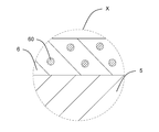
- the wavelength conversion member 6 may include a plurality of phosphors 60.
- the phosphor 60 converts light having a peak wavelength (excitation peak wavelength ⁇ e) in the wavelength region of 360 nm to 430 nm into light having a peak wavelength (emission peak wavelength ⁇ L) in the wavelength region of 610 nm to 730 nm.
- the wavelength conversion member 6 is provided at a position capable of converting the light emitted by the light emitting element 3 into light having a peak wavelength in the wavelength region of 610 nm to 730 nm.
- the wavelength region of 610 nm to 730 nm is included in the visible light region.
- the phosphor 60 may include a phosphor having a peak wavelength in the wavelength region of 600 nm to 660 nm.
- Examples of the phosphor having a peak wavelength in the wavelength region of 600 nm to 660 nm are a phosphor exhibiting red color.
- As the phosphor showing a red color for example, Y 2 O 2 S: Eu, Y 2 O 3 : Eu, SrCaClAlSiN 3 : Eu 2+ , CaAlSiN 3 : Eu, or CaAlSi (ON) 3 : Eu can be used.
- the red phosphor converts the light incident on the inside of the wavelength conversion member 6 into light having a peak wavelength in the wavelength region of 600 nm to 660 nm, and emits the converted light.
- the wavelength conversion member 6 may include, for example, a phosphor that exhibits a color in the near infrared region and has a peak wavelength in the wavelength region of 680 nm to 800 nm, in addition to the above-mentioned phosphor that exhibits red color.
- Examples of the phosphor exhibiting a color in the near infrared region include 3Ga 5 O 12 : Cr and the like. By selecting one of these phosphors or combining some of them, a phosphor 60 having an emission peak wavelength ⁇ L in the range of 610 nm to 730 nm can be obtained.
- the relative light intensity in the blue wavelength region described later is small (0.1 or less), so that the case where a blue emitting LED is used is used.
- the reproducibility of red light having an emission peak wavelength ⁇ L in the range of 610 nm to 730 nm can be improved.
- other phosphors as described above may be contained in a very small amount so as not to affect the emission peak wavelength ⁇ L. By containing a small amount of a phosphor other than red, it is possible to bring it closer to a natural color.
- the above-mentioned peak wavelength and the later-described peak wavelength refer to those whose spectrum shows a maximum value, that is, the wavelength of a peak in the valley of the spectrum.
- the spectrum may have tiny peaks and valleys when emitting various colors with the fluorophore. Such minute peaks and valleys are not used to identify peak wavelengths. That is, for example, the maximum value when the width from valley to valley is 20 nm or less may not be regarded as a peak.
- the emission spectra of the illumination device 10 and the light emitting device 1 of the present disclosure have an excitation peak wavelength ⁇ e in the wavelength region of 360 nm to 430 nm and an emission peak wavelength ⁇ L in the wavelength region of 610 nm to 730 nm.
- the relative light intensity at the excitation peak wavelength ⁇ e is 0.05 to 0.3
- the relative light intensity at 440 nm to 480 nm is 0.1 or less. Is good.
- it is preferable that the light intensity in the wavelength region from 480 nm to the emission peak wavelength ⁇ L is continuously increased.
- the excitation peak wavelength ⁇ e is the excitation light of the light emitting element 3.
- the relative light intensity of the excitation light is 0.05 to 0.3, even if direct purple light is emitted to the outside as leakage light, the effect on the color of the light to be emitted is small. In addition, the emission intensity can be sufficiently maintained. Further, since the relative light intensity in the range of 440 nm to 480 nm is 0.1 or less, the blue color that humans perceive is hardly contained, so that the influence on the color of the emitted light is small and the reproduction rate of the target light is improved. .. Since the light intensity in the wavelength region from 480 nm to the emission peak wavelength ⁇ L is continuously increased, there is no peak wavelength in the wavelength region, so that the color near the emission peak wavelength ⁇ L is preferably reproduced. be able to.
- the continuous increase in light intensity in the wavelength region from 480 nm to the emission peak wavelength ⁇ L means that the spectrum does not have a maximum value in the wavelength region from 480 nm to the emission peak wavelength ⁇ L, for example. Point to. As described above, the spectrum may have minute peaks and valleys, but such minute peaks and valleys need not be used when specifying the maximum value referred to here.
- the emission spectra of the lighting device 10 and the light emitting device 1 according to the first to third embodiments of the present disclosure will be specifically described with reference to FIGS. 6 to 8.
- the lighting device 10 and the light emitting device 1 according to the first to third embodiments are different in the material, the amount, and the like constituting the phosphor 60.
- the emission spectrum is measured by spectroscopic methods using, for example, a spectrophotometer.
- the lighting device 10 and the light emitting device 1 according to the first to third embodiments are devices that emit light color imitating the light color of a candle. Therefore, FIGS. 6 to 8 show a comparison between the actually measured value of the candle light and the measured value of each embodiment.
- the emission peak wavelength ⁇ L in each embodiment is the emission peak wavelength ⁇ L1 in the first embodiment, the emission peak wavelength ⁇ L2 in the second embodiment, and the emission peak wavelength ⁇ L3 in the third embodiment.
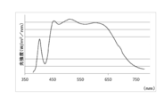
- the emission spectrum of the first embodiment has an emission peak wavelength ⁇ L1 in the wavelength region of 610 nm to 650 nm.
- the emission peak wavelength ⁇ L1 is located near 630 nm.
- the emission peak wavelength ⁇ L1 corresponds to the wavelength of the light emitted by the phosphor 60.
- the phosphor 60 mainly contains the above-mentioned red phosphor 60.
- the relative light intensity at the second peak wavelength ⁇ 2 in the present embodiment is about 0.26, and the relative light intensity at 440 nm to 480 nm is 0.1 or less.
- the lighting device 10 and the light emitting device 1 according to the first embodiment can realize bright light having a clearer red color as compared with other embodiments.
- the emission spectrum of the second embodiment has an emission peak wavelength ⁇ L2 in the wavelength region of 620 nm to 670 nm.
- the emission peak wavelength ⁇ L2 is located near 645 nm.
- the emission peak wavelength ⁇ L2 corresponds to the wavelength of the light emitted by the phosphor 60.
- the phosphor 60 mainly contains the above-mentioned red phosphor 60.
- the relative light intensity at the second peak wavelength ⁇ 2 in the present embodiment is about 0.25, and the relative light intensity at 440 nm to 480 nm is 0.09 or less.
- the lighting device 10 and the light emitting device 1 according to the second embodiment can be made to have a good balance of brightness and a color temperature close to that of candle light.
- the emission spectrum of the third embodiment has an emission peak wavelength ⁇ L3 in the wavelength region of 690 nm to 730 nm.
- the emission peak wavelength ⁇ L3 is located near 715 nm.
- the emission peak wavelength ⁇ L3 corresponds to the wavelength of the light emitted by the phosphor 60.
- the phosphor 60 mainly contains the phosphor 60 having a color in the near infrared region described above.
- the relative light intensity at the second peak wavelength ⁇ 2 in the present embodiment is about 0.06, and the relative light intensity at 440 nm to 480 nm is 0.08 or less.
- the light intensity in the wavelength region from 480 nm to the emission peak wavelength ⁇ L3 is continuously increasing, so that there is no peak wavelength during this period. Therefore, it is possible to reproduce a color near the emission peak wavelength ⁇ L3, that is, 690 nm to 730 nm.
- the lighting device 10, the lighting device 10, and the light emitting device 1 according to the third embodiment can realize light according to the measured value of the candle light, that is, light having a high recall rate.
- the emission spectrum of the light emitted by the lighting device 10 and the light emitting device 1 of the present disclosure contains almost no blue light perceived by humans due to the above-described configuration, the blue light is emitted. It has little effect on the color of light.
- the recall rate of the target light color red
- the light emitting device 1 of the second embodiment reproduces a light emitting device 1 closer to the light of the candle from the balance of brightness and the reproduction rate of the color temperature. be able to.
- Color rendering is one of the indexes for evaluating the quality of a light source, and the appearance of color is quantified by the number of color rendering evaluations based on natural light.
- the color rendering index is average color rendering index Ra, special color rendering index R9, special color rendering index R10, special color rendering index R11, special color rendering index R12, special color rendering index R13, special color rendering index R14, special color rendering evaluation. It can be represented by the number R15, etc.
- the lighting device 10 and the light emitting device 1 according to the present disclosure can realize the light emitting device 1 having excellent color rendering properties having an average color rendering index Ra of 85 or more.
- the lighting device 10 and the light emitting device 1 of the first embodiment have an average color rendering index Ra of 88.0
- the lighting device 10 and the light emitting device 1 of the second embodiment have an average color rendering index Ra of 88
- the lighting device 10 and the light emitting device 1 of the third embodiment have an average color rendering index Ra of 88.4.
- the color temperature is a numerical value of the color of light emitted by a light source, and is expressed in a unit of K (Kelvin).
- a low color temperature means that the color of the light emitted by the light source is reddish.
- a high color temperature means that the color of the light emitted by the light source is bluish.
- the color temperature of the light emitted by an incandescent light bulb is about 2800K.
- the color temperature of neutral white light is about 4200K.
- the light specified in the emission spectra of the lighting device 10 and the light emitting device 1 according to the first embodiment has a color temperature of 2083K.
- the light specified in the emission spectra of the lighting device 10 and the light emitting device 1 according to the second embodiment has a color temperature of 1964K.
- the light specified in the emission spectra of the lighting device 10 and the light emitting device 1 according to the third embodiment has a color temperature of 1825K.
- the emission spectra of the lighting device 10 and the light emitting device 1 according to the first to third embodiments show about 2000K of 1800K to 2100K including the measurement variation, and reproduce a warm red color like a Japanese candle. be able to.
- the lighting device 10 provided with at least one light emitting device 1 for reproducing the light of a Japanese candle is provided with a control unit 7 for adjusting the light intensity (dimming rate) of the light emitting device 1 in the same manner as described above. You may be.
- the control unit 7 can adjust the intensity of the light emitted from the light emitting device 1 by controlling the value of the current flowing through the light emitting device 1. Further, the control unit 7 can adjust the light emitted from the light emitting device 1 so as to fluctuate by changing the dimming rate with time or randomly changing the dimming rate. ..
- the control unit 7 may be attached to the wiring board 12 together, or the lighting device 10 is provided with a receiving unit and gives a command to a portion that controls the current of the wiring board 12 or the like by wireless communication from the outside. It may be something to put out.
- the lighting device 10 can reproduce light with different strengths (brightness and darkness) even if the light has the same color temperature.
- the lighting device 10 of the present disclosure can reproduce the light of a candle (Japanese candle).
- the lighting device 10 is used as lighting for illuminating temple pillars, Japanese paintings, walls, and the like, and you can experience the colors seen under the light of candles.
- the intensity of the light it is possible to reproduce a change such as a fluctuation of a candle.
- the lighting device 10 may be used not only indoors such as in a building or inside a house, but also outdoors.
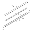
- the lighting device 10 includes a long housing 11 that is open upward, and a light emitting device 1 that is arranged in a plurality of lines in the housing 11 along the longitudinal direction.
- a long wiring board 12 on which a plurality of light emitting devices 1 are mounted, and a long translucent board 13 supported by the housing 11 and closing the opening of the housing 11 are provided.
- the housing 11 has a function of holding the translucent substrate 13 and a function of dissipating the heat generated by the light emitting device 1 to the outside.
- the housing 11 is made of, for example, a metal such as aluminum, copper or stainless steel, plastic or resin.
- the housing 11 is erected from a bottom portion 21a extending in the longitudinal direction and both ends in the width direction of the bottom portion 21a. Further, it has a pair of support portions 21b extending in the longitudinal direction and closes the long main body portion 21 which is open on both the upper and longitudinal directions and the openings on one side and the other side in the longitudinal direction of the main body portion 21, respectively. It is composed of two lids 22.
- a holding portion formed so that recesses for holding the translucent substrate 13 face each other is provided on the upper portion of each support portion 21b inside the housing 11.
- the length of the housing 11 in the longitudinal direction is set to, for example, 100 mm or more and 2000 mm or less.
- the wiring board 12 is fixed to the bottom surface inside the housing 11.
- a printed circuit board such as a rigid board, a flexible board, or a rigid flexible board is used.
- the wiring pattern of the wiring board 12 and the wiring pattern of the board 2 in the light emitting device 1 are electrically connected via solder or a conductive adhesive. Then, the signal from the wiring board 12 is transmitted to the light emitting element 3 via the board 2, and the light emitting element 3 emits light. Power is supplied to the wiring board 12 from an external power source via wiring.
- the translucent substrate 13 is made of a material that transmits light emitted from the light emitting device 1, and is made of, for example, a light transmissive material such as acrylic resin or glass.
- the translucent substrate 13 is a rectangular plate body, and the length in the longitudinal direction is set to, for example, 98 mm or more and 1998 mm or less.
- the translucent substrate 13 is inserted into the recess formed in each of the above-mentioned support portions 21b through an opening on one side or the other side in the longitudinal direction of the main body portion 21. Then, by sliding along the longitudinal direction, it is supported by a pair of support portions 21b at positions away from the plurality of light emitting devices 1. Then, the lighting device 10 is configured by closing the openings on one side and the other side in the longitudinal direction of the main body 21 with the lid 22.
- the above-mentioned lighting device 10 is a linear light emitting lighting device in which a plurality of light emitting devices 1 are linearly arranged, but the present invention is not limited to this, and a surface in which a plurality of light emitting devices 1 are arranged in a matrix or a houndstooth pattern. It may be a light emitting lighting device.
- each of the second light emitting devices 1b of the lighting device 10 has a bluish-green phosphor that emits blue fluorescence as a fluorescent substance contained in one wavelength conversion member 6.
- One of five types of phosphors consisting of a fluorescent substance that emits fluorescence, a fluorescent substance that emits green fluorescence, a fluorescent substance that emits red fluorescence, and a phosphor that emits fluorescence in the near infrared region, or among them.
- the configuration includes a plurality of the above, the configuration is not limited to this, and two types of wavelength conversion members may be provided.
- the first wavelength conversion member may be used, and different phosphors may be dispersed in the second wavelength conversion member, or different combinations may be used to disperse the phosphors. Then, these two wavelength conversion members may be provided in one light emitting device, and the light emitted through the respective wavelength conversion members may be mixed. By doing so, it is possible to easily control the color rendering property of the emitted light.
Landscapes
- Engineering & Computer Science (AREA)
- General Engineering & Computer Science (AREA)
- Physics & Mathematics (AREA)
- Spectroscopy & Molecular Physics (AREA)
- Microelectronics & Electronic Packaging (AREA)
- Led Device Packages (AREA)
- Circuit Arrangement For Electric Light Sources In General (AREA)
- Fastening Of Light Sources Or Lamp Holders (AREA)
Priority Applications (4)
| Application Number | Priority Date | Filing Date | Title |
|---|---|---|---|
| EP20850426.6A EP4012256A4 (en) | 2019-08-07 | 2020-08-06 | LIGHTING DEVICE |
| CN202080056409.9A CN114207346B (zh) | 2019-08-07 | 2020-08-06 | 照明装置 |
| JP2021537382A JP7270044B2 (ja) | 2019-08-07 | 2020-08-06 | 照明装置 |
| US17/632,898 US12000585B2 (en) | 2019-08-07 | 2020-08-06 | Lighting device |
Applications Claiming Priority (4)
| Application Number | Priority Date | Filing Date | Title |
|---|---|---|---|
| JP2019-145471 | 2019-08-07 | ||
| JP2019145471 | 2019-08-07 | ||
| JP2019-226564 | 2019-12-16 | ||
| JP2019226564 | 2019-12-16 |
Publications (1)
| Publication Number | Publication Date |
|---|---|
| WO2021025120A1 true WO2021025120A1 (ja) | 2021-02-11 |
Family
ID=74503637
Family Applications (1)
| Application Number | Title | Priority Date | Filing Date |
|---|---|---|---|
| PCT/JP2020/030205 Ceased WO2021025120A1 (ja) | 2019-08-07 | 2020-08-06 | 照明装置 |
Country Status (5)
| Country | Link |
|---|---|
| US (1) | US12000585B2 (https=) |
| EP (1) | EP4012256A4 (https=) |
| JP (3) | JP7270044B2 (https=) |
| CN (1) | CN114207346B (https=) |
| WO (1) | WO2021025120A1 (https=) |
Cited By (2)
| Publication number | Priority date | Publication date | Assignee | Title |
|---|---|---|---|---|
| US11655963B2 (en) | 2021-04-26 | 2023-05-23 | Nichia Corporation | Light emitting device, light fixture, and street light |
| US12163632B2 (en) | 2021-04-26 | 2024-12-10 | Nichia Corporation | Light emitting device, light fixture, and street light |
Citations (5)
| Publication number | Priority date | Publication date | Assignee | Title |
|---|---|---|---|---|
| JPS6363061B2 (https=) * | 1982-02-12 | 1988-12-06 | ||
| JP2010182724A (ja) * | 2009-02-03 | 2010-08-19 | Mitsubishi Electric Corp | 発光装置 |
| JP2013012778A (ja) * | 2011-06-02 | 2013-01-17 | Mitsubishi Chemicals Corp | 照明器具 |
| JP2015126160A (ja) | 2013-12-27 | 2015-07-06 | サンケン電気株式会社 | 発光装置 |
| JP2017136396A (ja) * | 2017-03-15 | 2017-08-10 | 富士フイルム株式会社 | 内視鏡システム |
Family Cites Families (25)
| Publication number | Priority date | Publication date | Assignee | Title |
|---|---|---|---|---|
| EP1790199B1 (en) * | 2004-06-29 | 2013-08-14 | Panasonic Corporation | Illumination source |
| US7404652B2 (en) | 2004-12-15 | 2008-07-29 | Avago Technologies Ecbu Ip Pte Ltd | Light-emitting diode flash module with enhanced spectral emission |
| JP2010508651A (ja) * | 2006-10-31 | 2010-03-18 | ティーアイアール テクノロジー エルピー | 光励起可能媒体を含む光源 |
| US7703943B2 (en) * | 2007-05-07 | 2010-04-27 | Intematix Corporation | Color tunable light source |
| US8740400B2 (en) * | 2008-03-07 | 2014-06-03 | Intematix Corporation | White light illumination system with narrow band green phosphor and multiple-wavelength excitation |
| US8021021B2 (en) * | 2008-06-26 | 2011-09-20 | Telelumen, LLC | Authoring, recording, and replication of lighting |
| US8459855B2 (en) * | 2008-07-28 | 2013-06-11 | Munisamy Anandan | UV LED based color pixel backlight incorporating quantum dots for increasing color gamut of LCD |
| US8534857B2 (en) * | 2009-10-26 | 2013-09-17 | Panasonic Corporation | Backlight apparatus, light source for backlight apparatus, and display apparatus using the same |
| US8511851B2 (en) * | 2009-12-21 | 2013-08-20 | Cree, Inc. | High CRI adjustable color temperature lighting devices |
| JP2010095728A (ja) * | 2009-12-28 | 2010-04-30 | Mitsubishi Chemicals Corp | 蛍光体及びその製造方法 |
| DE102010034054A1 (de) * | 2010-08-11 | 2012-02-16 | Schott Ag | Laserbasierte Weißlichtquelle |
| CN102458019B (zh) * | 2010-10-26 | 2014-01-22 | 财团法人工业技术研究院 | 光色调制方法及发光二极管光源模块 |
| JP5105132B1 (ja) * | 2011-06-02 | 2012-12-19 | 三菱化学株式会社 | 半導体発光装置、半導体発光システムおよび照明器具 |
| US8928249B2 (en) * | 2011-08-25 | 2015-01-06 | Abl Ip Holding Llc | Reducing lumen variability over a range of color temperatures of an output of tunable-white LED lighting devices |
| WO2013150470A1 (en) | 2012-04-06 | 2013-10-10 | Koninklijke Philips N.V. | White light emitting module |
| JP2012191225A (ja) * | 2012-05-23 | 2012-10-04 | Mitsubishi Electric Corp | 発光装置 |
| EP3176836B1 (en) * | 2012-10-04 | 2024-04-10 | Seoul Semiconductor Co., Ltd. | White light emitting device, lighting system, and dental lighting system |
| US9133990B2 (en) | 2013-01-31 | 2015-09-15 | Dicon Fiberoptics Inc. | LED illuminator apparatus, using multiple luminescent materials dispensed onto an array of LEDs, for improved color rendering, color mixing, and color temperature control |
| CN105074320B (zh) * | 2013-03-11 | 2019-05-14 | 飞利浦照明控股有限公司 | 具有改进的光特性的发光二极管模块 |
| JP6145679B2 (ja) * | 2013-10-28 | 2017-06-14 | パナソニックIpマネジメント株式会社 | 光源モジュール及び照明装置 |
| JP2017502493A (ja) * | 2013-10-28 | 2017-01-19 | ジーイー・ライティング・ソルーションズ,エルエルシー | 向上された蛍光増白及び色彩選好のためのランプ |
| JP2017523600A (ja) * | 2014-06-10 | 2017-08-17 | フィリップス ライティング ホールディング ビー ヴィ | 調整可能な発光スペクトルを持つ発光装置 |
| JP6384302B2 (ja) | 2014-12-05 | 2018-09-05 | 日亜化学工業株式会社 | 発光装置 |
| CN104633595B (zh) * | 2015-02-09 | 2016-02-24 | 常州千明智能照明科技有限公司 | 一种以高显色指数模拟日光的led灯具 |
| EP3367448B1 (en) * | 2015-10-20 | 2021-04-28 | Kyocera Corporation | Indoor light source and illumination device |
-
2020
- 2020-08-06 US US17/632,898 patent/US12000585B2/en active Active
- 2020-08-06 WO PCT/JP2020/030205 patent/WO2021025120A1/ja not_active Ceased
- 2020-08-06 CN CN202080056409.9A patent/CN114207346B/zh active Active
- 2020-08-06 EP EP20850426.6A patent/EP4012256A4/en active Pending
- 2020-08-06 JP JP2021537382A patent/JP7270044B2/ja active Active
-
2023
- 2023-04-24 JP JP2023071026A patent/JP7648672B2/ja active Active
-
2025
- 2025-03-06 JP JP2025035901A patent/JP2025078800A/ja active Pending
Patent Citations (5)
| Publication number | Priority date | Publication date | Assignee | Title |
|---|---|---|---|---|
| JPS6363061B2 (https=) * | 1982-02-12 | 1988-12-06 | ||
| JP2010182724A (ja) * | 2009-02-03 | 2010-08-19 | Mitsubishi Electric Corp | 発光装置 |
| JP2013012778A (ja) * | 2011-06-02 | 2013-01-17 | Mitsubishi Chemicals Corp | 照明器具 |
| JP2015126160A (ja) | 2013-12-27 | 2015-07-06 | サンケン電気株式会社 | 発光装置 |
| JP2017136396A (ja) * | 2017-03-15 | 2017-08-10 | 富士フイルム株式会社 | 内視鏡システム |
Non-Patent Citations (1)
| Title |
|---|
| See also references of EP4012256A4 |
Cited By (2)
| Publication number | Priority date | Publication date | Assignee | Title |
|---|---|---|---|---|
| US11655963B2 (en) | 2021-04-26 | 2023-05-23 | Nichia Corporation | Light emitting device, light fixture, and street light |
| US12163632B2 (en) | 2021-04-26 | 2024-12-10 | Nichia Corporation | Light emitting device, light fixture, and street light |
Also Published As
| Publication number | Publication date |
|---|---|
| CN114207346B (zh) | 2024-11-05 |
| CN114207346A (zh) | 2022-03-18 |
| EP4012256A4 (en) | 2023-09-13 |
| JP7270044B2 (ja) | 2023-05-09 |
| US20220268423A1 (en) | 2022-08-25 |
| JP2025078800A (ja) | 2025-05-20 |
| US12000585B2 (en) | 2024-06-04 |
| JPWO2021025120A1 (https=) | 2021-02-11 |
| JP2023095896A (ja) | 2023-07-06 |
| JP7648672B2 (ja) | 2025-03-18 |
| EP4012256A1 (en) | 2022-06-15 |
Similar Documents
| Publication | Publication Date | Title |
|---|---|---|
| JP6913790B2 (ja) | 屋内用光源および照明装置 | |
| RU2662240C2 (ru) | Светоизлучающая структура с адаптированным выходным спектром | |
| JP2002057376A (ja) | Ledランプ | |
| JP2017523600A (ja) | 調整可能な発光スペクトルを持つ発光装置 | |
| JP5443959B2 (ja) | 照明装置 | |
| TW201205892A (en) | LED-based light emitting systems and devices | |
| US10854792B2 (en) | Light-emitting device and illumination apparatus | |
| JP2025078800A (ja) | 照明装置 | |
| JP2008270701A (ja) | 発光装置および照明器具 | |
| JP2000164931A (ja) | 白色光源 | |
| JP2022103159A (ja) | 発光装置、照明装置および生物育成用の照明装置 | |
| JP2014150293A (ja) | 発光装置 | |
| JP2011119390A (ja) | 発光装置 | |
| JP3243360U (ja) | 生物育成用の照明装置 | |
| US11495716B2 (en) | Light-emitting device and illumination apparatus | |
| JP7233559B2 (ja) | 発光装置及び照明装置 | |
| JP2019117729A (ja) | 照明装置および照明モジュール | |
| WO2013011409A1 (en) | Incandescent lamp resembling lighting device | |
| JPWO2019107281A1 (ja) | 発光装置および照明装置 | |
| WO2020022492A1 (ja) | 照明装置および照明システム | |
| JP2020107422A (ja) | 照明装置および照明システム |
Legal Events
| Date | Code | Title | Description |
|---|---|---|---|
| 121 | Ep: the epo has been informed by wipo that ep was designated in this application |
Ref document number: 20850426 Country of ref document: EP Kind code of ref document: A1 |
|
| ENP | Entry into the national phase |
Ref document number: 2021537382 Country of ref document: JP Kind code of ref document: A |
|
| NENP | Non-entry into the national phase |
Ref country code: DE |
|
| ENP | Entry into the national phase |
Ref document number: 2020850426 Country of ref document: EP Effective date: 20220307 |