WO2021024288A1 - 半導体レーザ装置 - Google Patents
半導体レーザ装置 Download PDFInfo
- Publication number
- WO2021024288A1 WO2021024288A1 PCT/JP2019/030401 JP2019030401W WO2021024288A1 WO 2021024288 A1 WO2021024288 A1 WO 2021024288A1 JP 2019030401 W JP2019030401 W JP 2019030401W WO 2021024288 A1 WO2021024288 A1 WO 2021024288A1
- Authority
- WO
- WIPO (PCT)
- Prior art keywords
- diffraction grating
- unit
- laser
- semiconductor laser
- semiconductor substrate
- Prior art date
- Legal status (The legal status is an assumption and is not a legal conclusion. Google has not performed a legal analysis and makes no representation as to the accuracy of the status listed.)
- Ceased
Links
Images





Classifications
-
- H—ELECTRICITY
- H01—ELECTRIC ELEMENTS
- H01S—DEVICES USING THE PROCESS OF LIGHT AMPLIFICATION BY STIMULATED EMISSION OF RADIATION [LASER] TO AMPLIFY OR GENERATE LIGHT; DEVICES USING STIMULATED EMISSION OF ELECTROMAGNETIC RADIATION IN WAVE RANGES OTHER THAN OPTICAL
- H01S5/00—Semiconductor lasers
- H01S5/02—Structural details or components not essential to laser action
- H01S5/026—Monolithically integrated components, e.g. waveguides, monitoring photo-detectors, drivers
- H01S5/0265—Intensity modulators
-
- H—ELECTRICITY
- H01—ELECTRIC ELEMENTS
- H01S—DEVICES USING THE PROCESS OF LIGHT AMPLIFICATION BY STIMULATED EMISSION OF RADIATION [LASER] TO AMPLIFY OR GENERATE LIGHT; DEVICES USING STIMULATED EMISSION OF ELECTROMAGNETIC RADIATION IN WAVE RANGES OTHER THAN OPTICAL
- H01S5/00—Semiconductor lasers
- H01S5/06—Arrangements for controlling the laser output parameters, e.g. by operating on the active medium
- H01S5/0601—Arrangements for controlling the laser output parameters, e.g. by operating on the active medium comprising an absorbing region
-
- H—ELECTRICITY
- H01—ELECTRIC ELEMENTS
- H01S—DEVICES USING THE PROCESS OF LIGHT AMPLIFICATION BY STIMULATED EMISSION OF RADIATION [LASER] TO AMPLIFY OR GENERATE LIGHT; DEVICES USING STIMULATED EMISSION OF ELECTROMAGNETIC RADIATION IN WAVE RANGES OTHER THAN OPTICAL
- H01S5/00—Semiconductor lasers
- H01S5/06—Arrangements for controlling the laser output parameters, e.g. by operating on the active medium
- H01S5/062—Arrangements for controlling the laser output parameters, e.g. by operating on the active medium by varying the potential of the electrodes
- H01S5/0625—Arrangements for controlling the laser output parameters, e.g. by operating on the active medium by varying the potential of the electrodes in multi-section lasers
-
- H—ELECTRICITY
- H01—ELECTRIC ELEMENTS
- H01S—DEVICES USING THE PROCESS OF LIGHT AMPLIFICATION BY STIMULATED EMISSION OF RADIATION [LASER] TO AMPLIFY OR GENERATE LIGHT; DEVICES USING STIMULATED EMISSION OF ELECTROMAGNETIC RADIATION IN WAVE RANGES OTHER THAN OPTICAL
- H01S5/00—Semiconductor lasers
- H01S5/10—Construction or shape of the optical resonator, e.g. extended or external cavity, coupled cavities, bent-guide, varying width, thickness or composition of the active region
- H01S5/12—Construction or shape of the optical resonator, e.g. extended or external cavity, coupled cavities, bent-guide, varying width, thickness or composition of the active region the resonator having a periodic structure, e.g. in distributed feedback [DFB] lasers
- H01S5/1203—Construction or shape of the optical resonator, e.g. extended or external cavity, coupled cavities, bent-guide, varying width, thickness or composition of the active region the resonator having a periodic structure, e.g. in distributed feedback [DFB] lasers over only a part of the length of the active region
-
- H—ELECTRICITY
- H01—ELECTRIC ELEMENTS
- H01S—DEVICES USING THE PROCESS OF LIGHT AMPLIFICATION BY STIMULATED EMISSION OF RADIATION [LASER] TO AMPLIFY OR GENERATE LIGHT; DEVICES USING STIMULATED EMISSION OF ELECTROMAGNETIC RADIATION IN WAVE RANGES OTHER THAN OPTICAL
- H01S5/00—Semiconductor lasers
- H01S5/10—Construction or shape of the optical resonator, e.g. extended or external cavity, coupled cavities, bent-guide, varying width, thickness or composition of the active region
- H01S5/12—Construction or shape of the optical resonator, e.g. extended or external cavity, coupled cavities, bent-guide, varying width, thickness or composition of the active region the resonator having a periodic structure, e.g. in distributed feedback [DFB] lasers
- H01S5/1237—Lateral grating, i.e. grating only adjacent ridge or mesa
-
- H—ELECTRICITY
- H01—ELECTRIC ELEMENTS
- H01S—DEVICES USING THE PROCESS OF LIGHT AMPLIFICATION BY STIMULATED EMISSION OF RADIATION [LASER] TO AMPLIFY OR GENERATE LIGHT; DEVICES USING STIMULATED EMISSION OF ELECTROMAGNETIC RADIATION IN WAVE RANGES OTHER THAN OPTICAL
- H01S5/00—Semiconductor lasers
- H01S5/20—Structure or shape of the semiconductor body to guide the optical wave ; Confining structures perpendicular to the optical axis, e.g. index or gain guiding, stripe geometry, broad area lasers, gain tailoring, transverse or lateral reflectors, special cladding structures, MQW barrier reflection layers
- H01S5/22—Structure or shape of the semiconductor body to guide the optical wave ; Confining structures perpendicular to the optical axis, e.g. index or gain guiding, stripe geometry, broad area lasers, gain tailoring, transverse or lateral reflectors, special cladding structures, MQW barrier reflection layers having a ridge or stripe structure
- H01S5/227—Buried mesa structure ; Striped active layer
-
- H—ELECTRICITY
- H01—ELECTRIC ELEMENTS
- H01S—DEVICES USING THE PROCESS OF LIGHT AMPLIFICATION BY STIMULATED EMISSION OF RADIATION [LASER] TO AMPLIFY OR GENERATE LIGHT; DEVICES USING STIMULATED EMISSION OF ELECTROMAGNETIC RADIATION IN WAVE RANGES OTHER THAN OPTICAL
- H01S5/00—Semiconductor lasers
- H01S5/06—Arrangements for controlling the laser output parameters, e.g. by operating on the active medium
- H01S5/062—Arrangements for controlling the laser output parameters, e.g. by operating on the active medium by varying the potential of the electrodes
- H01S5/0625—Arrangements for controlling the laser output parameters, e.g. by operating on the active medium by varying the potential of the electrodes in multi-section lasers
- H01S5/06251—Amplitude modulation
-
- H—ELECTRICITY
- H01—ELECTRIC ELEMENTS
- H01S—DEVICES USING THE PROCESS OF LIGHT AMPLIFICATION BY STIMULATED EMISSION OF RADIATION [LASER] TO AMPLIFY OR GENERATE LIGHT; DEVICES USING STIMULATED EMISSION OF ELECTROMAGNETIC RADIATION IN WAVE RANGES OTHER THAN OPTICAL
- H01S5/00—Semiconductor lasers
- H01S5/10—Construction or shape of the optical resonator, e.g. extended or external cavity, coupled cavities, bent-guide, varying width, thickness or composition of the active region
- H01S5/12—Construction or shape of the optical resonator, e.g. extended or external cavity, coupled cavities, bent-guide, varying width, thickness or composition of the active region the resonator having a periodic structure, e.g. in distributed feedback [DFB] lasers
- H01S5/1206—Construction or shape of the optical resonator, e.g. extended or external cavity, coupled cavities, bent-guide, varying width, thickness or composition of the active region the resonator having a periodic structure, e.g. in distributed feedback [DFB] lasers having a non constant or multiplicity of periods
- H01S5/1212—Chirped grating
-
- H—ELECTRICITY
- H01—ELECTRIC ELEMENTS
- H01S—DEVICES USING THE PROCESS OF LIGHT AMPLIFICATION BY STIMULATED EMISSION OF RADIATION [LASER] TO AMPLIFY OR GENERATE LIGHT; DEVICES USING STIMULATED EMISSION OF ELECTROMAGNETIC RADIATION IN WAVE RANGES OTHER THAN OPTICAL
- H01S5/00—Semiconductor lasers
- H01S5/10—Construction or shape of the optical resonator, e.g. extended or external cavity, coupled cavities, bent-guide, varying width, thickness or composition of the active region
- H01S5/12—Construction or shape of the optical resonator, e.g. extended or external cavity, coupled cavities, bent-guide, varying width, thickness or composition of the active region the resonator having a periodic structure, e.g. in distributed feedback [DFB] lasers
- H01S5/1225—Construction or shape of the optical resonator, e.g. extended or external cavity, coupled cavities, bent-guide, varying width, thickness or composition of the active region the resonator having a periodic structure, e.g. in distributed feedback [DFB] lasers with a varying coupling constant along the optical axis
-
- H—ELECTRICITY
- H01—ELECTRIC ELEMENTS
- H01S—DEVICES USING THE PROCESS OF LIGHT AMPLIFICATION BY STIMULATED EMISSION OF RADIATION [LASER] TO AMPLIFY OR GENERATE LIGHT; DEVICES USING STIMULATED EMISSION OF ELECTROMAGNETIC RADIATION IN WAVE RANGES OTHER THAN OPTICAL
- H01S5/00—Semiconductor lasers
- H01S5/20—Structure or shape of the semiconductor body to guide the optical wave ; Confining structures perpendicular to the optical axis, e.g. index or gain guiding, stripe geometry, broad area lasers, gain tailoring, transverse or lateral reflectors, special cladding structures, MQW barrier reflection layers
- H01S5/22—Structure or shape of the semiconductor body to guide the optical wave ; Confining structures perpendicular to the optical axis, e.g. index or gain guiding, stripe geometry, broad area lasers, gain tailoring, transverse or lateral reflectors, special cladding structures, MQW barrier reflection layers having a ridge or stripe structure
- H01S5/227—Buried mesa structure ; Striped active layer
- H01S5/2275—Buried mesa structure ; Striped active layer mesa created by etching
Definitions
- the present application relates to a semiconductor laser device.
- a structure in which a diffraction grating is formed on the EA modulator has been reported (see, for example, Patent Document 1).
- a diffraction grating is formed in the entire waveguide in the EA modulator region, and a separation region in which the modulator electrode and the laser electrode are separated, that is, a distributed feedback type laser region.
- a diffraction grating is also formed in the region between the EA modulator region and the region.
- a diffraction grating is formed from the emission end at which the laser beam in the distributed feedback type laser region is emitted to the emission end in the EA modulator region. Since light is reflected by the diffraction grating, the semiconductor laser device of Patent Document 1 is emitted by the diffraction grating formed in the region between the distributed feedback type laser region and the EA modulator region and the EA modulator region. There is a problem that the light output of the laser beam is reduced.
- the technique disclosed in the present specification aims to increase the optical output of laser light in a semiconductor laser apparatus in which an EA modulator having a diffraction grating formed and a distributed feedback laser are integrated.
- the distribution feedback type laser unit and the electric field absorption type modulator unit are formed on the same semiconductor substrate, and the laser light emitted from the laser unit is a modulator.
- a semiconductor laser device that emits light from the emission end face of the unit, the laser unit includes a first diffraction grating formed by extending in the direction of the optical axis of the laser light, and the modulator unit includes at least a part of the laser.
- a second diffraction grating formed by extending in the direction of the optical axis of light is provided, and diffraction is performed between the second diffraction grating of the modulator unit and the emission end of the laser unit where the laser light is emitted to the modulator unit.
- a diffraction grating is not formed between the second diffraction grating of the modulator unit and the emission end of the laser unit where the laser light is emitted to the modulator unit. Since the non-diffraction grating region is interposed, the light output of the laser beam can be increased.
- FIG. It is a perspective view which shows the semiconductor laser apparatus which concerns on Embodiment 1.
- FIG. It is sectional drawing of the mesa stripe of the first example in the semiconductor laser apparatus of FIG. It is a figure which shows the diffraction grating in the modulator part of FIG. It is sectional drawing of the laser part in the semiconductor laser apparatus of FIG. It is sectional drawing of the modulator part in the semiconductor laser apparatus of FIG. It is sectional drawing of the modulator part in the semiconductor laser apparatus of FIG. It is sectional drawing of the separation part in the semiconductor laser apparatus of FIG. It is sectional drawing of the mesa stripe of the 2nd example in the semiconductor laser apparatus of FIG. It is sectional drawing of the mesa stripe of the 3rd example in the semiconductor laser apparatus of FIG.
- FIG. 1 is a perspective view showing a semiconductor laser device according to the first embodiment.
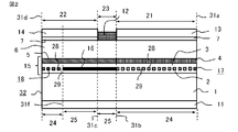
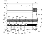
- FIG. 2 is a cross-sectional view of the mesa stripe of the first example in the semiconductor laser apparatus of FIG. 1
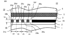
- FIG. 3 is a diagram showing a diffraction grating in the modulator section of FIG.
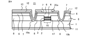
- FIG. 4 is a cross-sectional view of the laser section of the semiconductor laser device of FIG. 1, and FIGS.
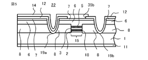
- FIG. 5 and 6 are cross-sectional views of the modulator section of the semiconductor laser device of FIG. 1, respectively.
- FIG. 7 is a cross-sectional view of a separation portion in the semiconductor laser device of FIG. 8 is a cross-sectional view of the second example of the mesa stripe in the semiconductor laser device of FIG. 1
- FIG. 9 is a cross-sectional view of the third example of the mesa stripe in the semiconductor laser device of FIG. 1
- FIG. 10 is FIG. It is sectional drawing of the 4th example mesa stripe in a semiconductor laser apparatus.
- FIG. 1 also shows a waveguide cross section 33 parallel to the z direction, which is the emission direction of the laser beam and the optical axis direction. 4 to 7 show a cross section perpendicular to the z direction.
- the semiconductor laser device 50 of the first embodiment includes a laser unit 21, a modulator unit 22, and a separation unit 23.
- a distributed feedback type laser is formed in the laser unit 21.
- the modulator unit 22 is an electric field absorption type (EA) modulator formed monocilically on the semiconductor substrate 1 of n-InP
- the semiconductor laser apparatus 50 is an electric field absorption type (EA) modulator integrated semiconductor laser.
- the laser unit 21 is formed in the region between the broken line 31a and the broken line 31b
- the separating unit 23 is formed in the region between the broken line 31b and the broken line 31c
- the modulator unit 22 is formed between the broken line 31c and the broken line 31d. It is formed in the area of.
- the semiconductor substrate 1 in which the distributed feedback type laser unit 21 and the electric field absorption type modulator unit 22 are the same is formed, and the laser light emitted from the laser unit 21 is modulated.
- This is a semiconductor laser device that is emitted from the emission end surface 32 of the instrument unit 22.
- the laser unit 21 is composed of a semiconductor substrate 1, a first clad layer 2 of n-InP, a diffraction lattice material layer 16 on which a diffraction lattice 17 is formed, a second clad layer 3 of n-InP, an active layer 4, and p-InP.
- the modulator unit 22 includes a semiconductor substrate 1, a first clad layer 2 of n-InP, a diffraction lattice material layer 16 in which a diffraction lattice 18 is partially formed, a second clad layer 3 of n-InP, and an absorption layer 5.
- the separation unit 23 is a structure of a region (separation region, isolation region) that separates the laser unit 21 and the modulator unit 22.
- the separation unit 23 includes a semiconductor substrate 1, a first clad layer 2 of n-InP, a diffraction grating material layer 16 on which a diffraction grating is not formed, a second clad layer 3 of n-InP, an absorption layer 5, and p-InP. and a third cladding layer 6, InP buried layer 8, Si0 2 insulating film 12, cathode electrode 11 formed on the back surface of the semiconductor substrate 1.
- a semiconductor substrate 1 a first clad layer 2 of n-InP
- a diffraction grating material layer 16 on which a diffraction grating is not formed a second clad layer 3 of n-InP, an absorption layer 5, and p-InP.
- a third cladding layer 6 InP buried layer 8, Si0 2 insulating
- the z direction is the direction of the optical axis of the laser beam emitted by the laser unit 21
- the x direction is the direction perpendicular to the z direction, and each layer included in the semiconductor laser device 50 is stretched, and the y direction is. This is the direction in which the layers included in the semiconductor laser apparatus 50 are laminated in the x-direction and in the x-direction.
- the active layer 4 is composed of InGaAsP multiple quantum wells.
- the absorption layer 5 is composed of an InGaAsP multiple quantum well.
- a diffraction grating 17 in which a recess 29 is formed in the diffraction grating material layer 16 of InGaAsP is formed between the lower layer of the active layer 4, that is, the first clad layer 2 and the second clad layer 3 on the semiconductor substrate 1 side. It is provided.
- the same InGaAsP diffraction grating material layer 16 as the laser unit 21 is formed, and a diffraction grating 18 having recesses 29a, 29b, 29c, and 29d formed in a part of the diffraction grating material layer 16 is provided.
- FIGS. 1 and 2 show an example in which the diffraction grating 18 is provided only on the side of the emission end surface 32 opposite to the laser unit 21.
- the separation portion 23 is also formed with the same InGaAsP diffraction grating material layer 16 as the laser portion 21, but is not provided with a diffraction grating having a recess 29 formed therein.
- the laser unit 21 is formed with a mesa stripe 15 which is a mesa extending in the direction of the optical axis (z direction) of the laser light emitted by the laser unit 21.
- the mesa stripe 15 of the laser unit 21 is composed of a part of the first clad layer 2, the diffraction grating material layer 16 on which the diffraction grating 17 is formed, the second clad layer 3, the active layer 4, and the third clad layer 6.
- a part of the third clad layer 6 constituting the mesa stripe 15 is a portion of the embedded layer 8 between the surface position on the opposite side of the semiconductor substrate 1 and the active layer 4.
- the mesa stripe 15 is continuously formed in the laser unit 21, the separation unit 23, and the modulator unit 22. Although the mesa stripe 15 is continuously formed, the mesa stripe 15 in the laser unit 21, the separation unit 23, and the modulator unit 22 is described separately from the first mesa stripe, the third mesa stripe, and the second mesa stripe, respectively. In some cases.
- the laser unit 21 includes a diffraction grating 17 which is a first diffraction grating formed by extending in the direction of the optical axis of the laser beam.
- the mesa stripe 15 of the modulator unit 22 is a part of the first clad layer 2, the diffraction grating material layer 16 including the portion where the diffraction grating 18 is formed, the second clad layer 3, the absorption layer 5, and the third clad layer 6. It is composed of.
- the mesa stripe 15 of the separation portion 23 is composed of a part of the first clad layer 2, the diffraction grating material layer 16 on which the diffraction grating is not formed, the second clad layer 3, the absorption layer 5, and the third clad layer 6. There is.
- a part of the third clad layer 6 constituting the mesa stripe 15 is a part of the embedded layer 8 between the surface position on the opposite side of the semiconductor substrate 1 and the absorption layer 5, and the modulator portion 22 is a portion of the laser beam.
- a diffraction grating 18 which is a second diffraction grating formed by extending in the direction of the optical axis is provided.
- Grooves 19a and 19b that penetrate the embedded layer 8 and the third clad layer 6 and reach the semiconductor substrate 1 are formed on both sides of the laser unit 21, the separation unit 23, and the modulator unit 22 in the mesa stripe 15 in the x direction. There is. In the laser unit 21 and the modulator unit 22, the grooves 19a and 19b also penetrate the contact layer 7.
- the insulating film 12 is formed on the surfaces of the contact layer 7 and the grooves 19a and 19b.
- the insulating film 12 is formed on the surfaces of the third clad layer 6 and the grooves 19a and 19b.
- the first anode electrode 13 of the laser unit 21 is connected to the contact layer 7 from the opening 35a formed in the insulating film 12.
- the second anode electrode 14 of the modulator unit 22 is connected to the contact layer 7 through the opening 35b formed in the insulating film 12.
- the film thickness ta of the diffraction grating material layer 16 between the first clad layer 2 and the second clad layer 3 is set in the laser unit 21, the separation unit 23, and the modulator unit 22. It is the same.
- the broken line 34a in FIG. 3 is a broken line showing the back surface of the diffraction grating material layer 16 (the surface on the semiconductor substrate 1 side), and the broken line 34b is the broken line showing the surface of the diffraction grating material layer 16 (the surface opposite to the semiconductor substrate 1). Is. As shown in FIG.
- the modulator unit 22 includes a diffraction grating region 24 in which the diffraction grating 18 is formed and a non-diffraction grating region 25 in which the diffraction grating 18 is not formed in the mesa stripe 15.
- the diffraction grating region 24 is a region from the broken line 31f to the broken line 31d
- the non-diffraction grating region 25 is a region from the broken line 31c to the broken line 31f.
- the diffraction grating 18 is formed on the side of the exit end surface 32
- the non-diffraction grating region 25 is provided on the side of the laser unit 21 in the modulator unit 22. As shown in FIG.
- the diffraction grating 18 includes four convex portions 28a, 28b, 28c, 28d and four concave portions 29a, 29b, 29c, 29d.
- the convex portions 28a, 28b, 28c, 28d of the modulator unit 22 extend in the direction perpendicular to the semiconductor substrate 1, and the concave portions 29a, 29b, 29c, 29d of the modulator unit 22 are the convex portions 28a of the modulator unit 22.
- 28b, 28c, 28d are recessed toward the semiconductor substrate 1 rather than the surface opposite to the semiconductor substrate 1.
- the thicknesses of the convex portions 28a, 28b, 28c, and 28d are the same, and the depths of the concave portions 29a, 29b, 29c, and 29d formed by cutting the diffraction grating material layer 16 are diffracted.
- An example is shown in which the film thickness ta of the grating material layer 16 is the same.
- the reference numerals of the convex portions are generally 28, and 28a, 28b, 28c, and 28d are used to distinguish them.
- 29 is used as a general reference for the recesses, and 29a, 29b, 29c, and 29d are used to distinguish them.
- the distance between the broken line 31f and the end of the convex portion 28a on the exit end surface 32 side is za
- the distance between the end of the convex portion 28a on the exit end surface 32 side and the end of the convex portion 28b on the exit end surface 32 side is
- the distance between the end of the convex portion 28b on the exit end surface 32 side and the end of the convex portion 28c on the exit end surface 32 side is zc
- the distance between the end of the convex portion 28c on the exit end surface 32 side and the exit end surface of the convex portion 28d is zc.
- the distance from the end on the 32 side is zd.
- the end of the convex portion 28d on the exit end surface 32 side and the exit end surface 32 coincide with each other.
- the spacing z, spacing zb, spacing zc, and spacing zd are the spacing between a set of adjacent convex portions 28 and 29, which are the same.
- FIG. 3 an example is shown in which the width of the convex portion 28 in the z direction and the width of the concave portion 29 in the z direction are the same.
- the period of the convex portion 28 and the concave portion 29 is the same over the entire diffraction grating. That is, in the diffraction grating 18 of the first embodiment, the period of the convex portion 28 and the concave portion 29 is uniform.
- a diffraction grating 17 is formed in the mesa stripe 15 over the entire z direction, that is, between the broken line 31a and the broken line 31b. That is, in the laser unit 21, there is no non-diffraction grating region 25 in which the diffraction grating is not formed in the mesa stripe 15, but only the diffraction grating region 24 in which the diffraction grating is formed. Further, the diffraction grating 17 of the laser unit 21 includes a plurality of convex portions 28 and a plurality of concave portions 29.
- the convex portion 28 of the laser portion 21 extends in the direction perpendicular to the semiconductor substrate 1, and the concave portion 29 of the laser portion 21 is the semiconductor substrate 1 rather than the surface of the convex portion 28 of the laser portion 21 opposite to the semiconductor substrate 1. It is dented on the side.
- FIG. 2 shows an example in which the depth of the recess 29 formed by scraping the diffraction grating material layer 16 is the same as the film thickness ta of the diffraction grating material layer 16.
- the distance between the adjacent set of convex portions 28 and the concave portion 29 in the diffraction grating 17 of the laser unit 21 is the distance between the adjacent set of convex portions 28 and the concave portion 29 in the diffraction grating 18 of the modulator unit 22. It is the same.
- the period of the convex portion 28 and the concave portion 29 is the same over the entire diffraction grating. That is, in the diffraction grating 17 of the first embodiment, the period of the convex portion 28 and the concave portion 29 is uniform.
- a diffraction grating is not formed over the entire z direction, that is, between the broken line 31b and the broken line 31c. That is, the separation unit 23 does not have the diffraction grating region 24 in which the diffraction grating is formed in the mesa stripe 15, but only the non-diffraction grating region 25 in which the diffraction grating is not formed.
- the semiconductor laser device 50 shown in FIG. 2 between the diffraction grating 18 of the modulator unit 22 and the emission end (end indicated by the broken line 31b) of the laser unit 21 at which the laser light is emitted to the modulator unit 22. It is a semiconductor laser apparatus in which a non-diffraction grating region 25 in which a diffraction grating is not formed is interposed.
- the first clad layer 2 and the diffraction grating material layer 16 are sequentially crystal-grown on the surface of the semiconductor substrate 1 by the MOCVD (Metal organic chemical vapor deposition) method, and recesses 29 are formed in the diffraction grating material layer 16 to form recesses 29 in the diffraction gratings 17 and 18.
- MOCVD Metal organic chemical vapor deposition
- a part of the second clad layer 3, the active layer 4, the absorption layer 5, and the third clad layer 6 is sequentially crystal-grown on the surface of the diffraction grating material layer 16 including the diffraction gratings 17 and 18 by the MOCVD method, and the SiO 2 is formed.
- the mesa stripe 15 is formed by dry etching using a mask. After that, the embedded layer 8 is crystal-grown on the exposed semiconductor substrate 1 on both sides of the mesa stripe 15.
- the mask of SiO 2 is removed, the third clad layer 6 and the contact layer 7 are sequentially crystal-grown on the surfaces of the embedded layer 8 and the mesa stripe 15, and the separation portion 23 is subjected to wet etching using a photoresist mask.
- the contact layer 7 on the surface is removed.
- grooves 19a and 19b are formed by wet etching using the photoresist mask.
- the mask of the photoresist is removed, and the insulating film 12 is formed on the surfaces of the third clad layer 6, the contact layer 7, and the grooves 19a and 19b of the separation portion 23.
- the openings 35a and 35b of the insulating film 12 are formed by using a photoresist mask.
- the photoresist mask is removed, and metal layers are formed on the front surface and the back surface of the semiconductor laser device 50 to form the cathode electrode 11, the first anode electrode 13, and the second anode electrode 14. After that, the insulating film 12 is thickly formed between the first anode electrode 13 and the second anode electrode 14.
- a semiconductor laser device semiconductor laser device of a comparative example
- semiconductor laser device of a comparative example in which an EA modulator and a distributed feedback laser are integrated and a diffraction grating is not formed in the region of the EA modulator
- the emission end face of the laser beam modulator side
- an adiabatic chapter in which the oscillation wavelength of the distributed feedback laser fluctuates is generated.
- this adiabatic chirp affects the transmission characteristics when an optical signal is transmitted in an optical fiber.
- the semiconductor laser device 50 of the first embodiment is provided with a diffraction grating 18 in the modulator unit 22. Therefore, in the semiconductor laser device 50 of the first embodiment, the phase of the reflected light of the laser light generated in front of the element of the semiconductor laser device 50, that is, at the emission end surface 32 starts on the laser unit 21 side of the diffraction grating 18 of the modulator unit.
- the semiconductor laser device 50 of the first embodiment can suppress variations in the amount of heat insulating chirp for each semiconductor laser device, and can avoid a decrease in transmission yield.
- the semiconductor laser device 50 of the first embodiment does not need to add a waveguide provided with a diffraction grating in front of the modulator unit 22, that is, on the side of the emission end surface 32. Therefore, the semiconductor laser device 50 of the first embodiment has a simpler manufacturing process and a smaller element size than the semiconductor laser device having a structure in which a waveguide having a diffraction grating is added, so that the cost can be reduced. It becomes.
- a diffraction grating is formed in the entire waveguide in the EA modulator region, and further, a diffraction grating is formed in the separation region in which the modulator electrode and the laser electrode are separated. There is. Since light is reflected in the diffraction grating, there is a problem that the light output of the laser light from the semiconductor laser apparatus decreases when the region of the diffraction grating becomes large.
- the semiconductor laser apparatus 50 of the first embodiment as shown in FIGS. 2 and 3, no diffraction grating is formed on the side of the laser unit 21 of the modulator unit 22 and the separation unit 23, that is, at least. Since the diffraction grating is not formed on the separation unit 23, it is possible to increase the light output of the laser light as compared with the semiconductor laser device of Patent Document 1.
- a non-diffraction grating region 25 is interposed between the end (emission end) from which the laser light of the laser unit 21 is emitted, that is, the end indicated by the broken line 31b to the diffraction grating 18 formed in the modulator unit 22. You just have to.
- the semiconductor laser device 50 provided with the mesa stripe 15 of the second example shown in FIG. 8 is an example in which the diffraction grating 18 is formed on the side of the laser unit 21 in the mesa stripe 15 of the modulator unit 22.
- the area between the broken line 31c and the broken line 31f is the diffraction grating region 24 in which the diffraction grating 18 is formed, and the broken line 31f to the broken line 31d Between the interval and between the broken line 31b and the broken line 31c is a non-diffraction grating region 25 in which the diffraction grating 18 is not formed.
- the semiconductor laser device 50 provided with the mesa stripe 15 of the third example shown in FIG. 9 is an example in which the diffraction grating 18 is formed in the central portion of the mesa stripe 15 of the modulator unit 22.
- the area between the broken line 31f and the broken line 31g is the diffraction grating region 24 in which the diffraction grating 18 is formed, and the broken line 31b to the broken line 31f
- the non-diffraction grating region 25 in which the diffraction grating 18 is not formed is between the interval and between the broken line 31g and the broken line 31d.
- the semiconductor laser device 50 provided with the mesa stripe 15 of the fourth example shown in FIG. 10 is an example in which the diffraction grating 18 is formed on the entire mesa stripe 15 of the modulator unit 22. Even in the semiconductor laser apparatus 50 provided with the mesa stripe 15 of the fourth example shown in FIG. 10, in the mesa stripe 15, the diffraction grating 18 is not formed between the emission end of the laser unit 21 and the emission end surface 32. Since the lattice region 25 exists, compared with the semiconductor laser device of Patent Document 1 in which a diffraction grating is formed from the emission end at which the laser light of the distributed feedback type laser region is emitted to the emission end of the EA modulator region. , The light output of the laser beam can be increased.
- the separation unit 23 is formed between the laser unit 21 and the modulator unit 22 has been described.
- the semiconductor laser apparatus 50 in which the separation portion 23 is not formed, in the mesa stripe 15, the non-diffraction grating region in which the diffraction grating 18 is not formed between the emission end and the emission end surface 32 of the laser portion 21 Any structure may be used as long as 25 is present.
- the mesa stripe 15 there is a non-diffraction grating region 25 in which the diffraction grating 18 is not formed between the emission end of the laser unit 21 and the emission end surface 32, so that the laser light in the distributed feedback laser region can be emitted.
- the semiconductor laser device 50 in which the separation unit 23 is not formed between the laser unit 21 and the modulator unit 22 has, for example, the contact layer 7 of the laser unit 21 and the modulator unit 22 as in the semiconductor laser apparatus of Patent Document 1. It is a device that does not separate with and (first example without a separation part). Further, in the semiconductor laser apparatus 50 in which the separation unit 23 is not formed between the laser unit 21 and the modulator unit 22, a step is provided between the laser unit 21 and the modulator unit 22, and the contact of the laser unit 21 is provided.
- the structure of the mesa stripe 15 of the fourth example shown in FIG. 10 cannot be applied.
- the distributed feedback type laser unit 21 and the electric field absorption type modulator unit 22 are formed on the same semiconductor substrate 1, and are emitted from the laser unit 21.
- This is a semiconductor laser device in which the laser beam is emitted from the emission end face 32 of the modulator unit 22.
- the laser unit 21 includes a first diffraction grating (diffraction grating 17) formed by extending in the direction of the optical axis of the laser light, and the modulator unit 22 has at least one.
- a second diffraction grating (diffraction grating 18) formed by extending in the direction of the optical axis of the laser beam is provided in the portion.
- FIG. 11 is a perspective view showing the semiconductor laser device according to the second embodiment
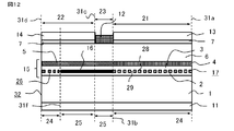
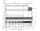
- FIG. 12 is a cross-sectional view of a mesa stripe in the semiconductor laser device of FIG. 13 is a diagram showing a diffraction grating in the modulator unit of FIG. 11, and
- FIG. 14 is a cross-sectional view of the modulator unit in the semiconductor laser apparatus of FIG.
- the semiconductor laser device 50 of the second embodiment is different from the semiconductor laser device 50 of the first embodiment in that a diffraction grating 26 having a non-uniform period is formed in the diffraction grating region 24 of the modulator unit 22. A portion different from the semiconductor laser device 50 of the first embodiment will be mainly described.
- the diffraction grating 26 includes four convex portions 28a, 28b, 28c, 28d and four concave portions 29a, 29b, 29c, 29d.
- the depths of the recesses 29a, 29b, 29c, and 29d formed by cutting the diffraction grating material layer 16 are the same as the film thickness ta of the diffraction grating material layer 16.
- the reference numerals of the convex portions are generally 28, and 28a, 28b, 28c, and 28d are used to distinguish them.
- 29 is used as a general reference for the recesses, and 29a, 29b, 29c, and 29d are used to distinguish them.
- the distance between the broken line 31f and the end of the convex portion 28a on the exit end surface 32 side is za
- the distance between the end of the convex portion 28a on the exit end surface 32 side and the end of the convex portion 28b on the exit end surface 32 side is
- the distance between the end of the convex portion 28b on the exit end surface 32 side and the end of the convex portion 28c on the exit end surface 32 side is zc
- the distance between the end of the convex portion 28c on the exit end surface 32 side and the exit end surface of the convex portion 28d The distance from the end on the 32 side is zd.
- the spacing z, spacing zb, spacing zc, and spacing zd are the spacing between a set of adjacent convex portions 28 and 29, which are different.
- the intervals za, zb, zc, and zd have the relationship of the equation (1), and an example is shown in which the width of the convex portion 28 in the z direction and the width of the concave portion 29 in the z direction are the same. zd>zc>zb> za ... (1)
- the distance between the convex portion 28 and the concave portion 29 is non-uniform with respect to the z direction, which is the emission direction of the laser beam. That is, in the diffraction grating 26 of the second embodiment, the periods of the convex portion 28 and the concave portion 29 are non-uniform.
- the semiconductor laser device 50 of the second embodiment provided with the non-uniform period diffraction grating 26 in the modulator unit 22 is the semiconductor laser device of the first embodiment provided with the uniform period diffraction grating 18 in the modulator unit 22.
- the wavelength band of light reflection generated by the diffraction grating can be expanded.
- the semiconductor laser device 50 of the second embodiment even if the driving conditions of the laser unit 21 or the modulator unit 22 change, or the element size of the semiconductor laser device 50 changes due to manufacturing variations, the laser unit The output light generated from 21 can be reliably reflected to the laser unit 21 side by the diffraction grating 26 of the modulator unit 22. That is, the semiconductor laser device 50 of the second embodiment can suppress the variation in the adiabatic chirp amount for each semiconductor laser device and can avoid a decrease in the transmission yield of the semiconductor laser device 50 of the first embodiment.
- the effect can be obtained even when the driving conditions are changed as compared with the semiconductor laser device 50 of the first embodiment and one or both of the cases where the manufacturing variation occurs. That is, the semiconductor laser device 50 of the second embodiment is more resistant to changes in driving conditions and manufacturing variations than the semiconductor laser device 50 of the first embodiment.
- the semiconductor laser device 50 of the second embodiment has the same structure as the semiconductor laser device 50 of the first embodiment except for the period of the diffraction grating of the modulator unit 22. Therefore, the semiconductor laser device 50 of the second embodiment emits light from the structure in which the diffraction grating 26 is not formed at least in the separation unit 23 or the emission end of the laser unit 21 as in the semiconductor laser device 50 of the first embodiment. Since it has a structure in which a non-diffraction grating region 25 in which a diffraction grating 26 is not formed exists up to the end face 32, the light output of the laser light is increased as compared with the semiconductor laser apparatus of Patent Document 1. Is possible.
- the semiconductor laser device 50 of the second embodiment includes the diffraction grating 26 having a non-uniform period in the mesa stripe 15 of the modulator unit 22, the reflected light generated in front of the element of the semiconductor laser device 50, that is, at the emission end surface 32 is emitted. Since the diffraction grating 26 of the modulator unit 22 in which the wavelength band of light reflection is widened moves toward a position away from the absorption layer 5 and the active layer 4, the reflected light from the front of the element propagates to the active layer 4 of the laser unit 21. It is possible to suppress the variation in the amount of the heat insulating charp for each semiconductor laser device, and it is possible to avoid a decrease in the transmission yield.
- the semiconductor laser device 50 of the second embodiment adds a waveguide provided with a diffraction grating to the front of the modulator unit 22, that is, to the side of the emission end face 32, similarly to the semiconductor laser device 50 of the first embodiment. There is no need. Therefore, the semiconductor laser device 50 of the second embodiment has a simpler manufacturing process and a smaller element size than the semiconductor laser device having a structure in which a waveguide having a diffraction grating is added, so that the cost can be reduced. It becomes.
- FIG. 15 is a perspective view showing the semiconductor laser device according to the third embodiment
- FIG. 16 is a view showing a diffraction grating of the first example in the modulator section of FIG. 15
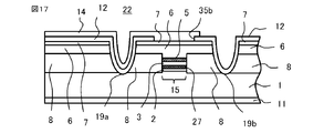
- FIG. 17 is a view showing the semiconductor laser device of FIG. It is sectional drawing of the modulator part in.
- FIG. 18 is a diagram showing a diffraction grating of the second example in the modulator section of FIG. 15, and
- FIG. 19 is a diagram showing a diffraction grating of the third example in the modulator section of FIG.
- the semiconductor laser device 50 of the third embodiment is implemented in that a diffraction grating 27 having a non-uniform depth of the recess 29 or the thickness of the convex portion 28 is formed in the diffraction grating region 24 of the modulator unit 22. It is different from the semiconductor laser apparatus 50 of the first embodiment. A portion different from the semiconductor laser device 50 of the first embodiment will be mainly described.
- the diffraction grating 27 includes six convex portions 28a, 28b, 28c, 28d, 28e, 28f and six concave portions 29a, 29b, 29c, 29d, 29e, 29f.
- the code of the convex portion uses 28 as a whole, and 28a, 28b, 28c, 28d, 28e, and 28f are used when distinguishing.
- 29 is used as a general reference for the concave portion, and 29a, 29b, 29c, 29d, 29e, and 29f are used to distinguish them.
- the convex portion 28 has the same film thickness ta as the diffraction grating material layer 16, and the depths of the recesses 29a, 29b, 29c, 29d, 29e, and 29f formed by cutting the diffraction grating material layer 16 are shown.
- An example that is not the same is shown. That is, in the diffraction grating 27 of the first example in the modulator unit 22 shown in FIG. 16, the thickness of the convex portion 28 is uniform, and the depth of the concave portion 29 formed by cutting the diffraction grating material layer 16 is This is an example of non-uniformity.
- the distance between the broken line 31f and the end of the convex portion 28a on the exit end surface 32 side is the same as the distance between the end of the convex portion 28e on the exit end surface 32 side and the end of the convex portion 28f on the exit end surface 32 side, zp. Is. It should be noted that the end of the convex portion 28f on the exit end surface 32 side and the exit end surface 32 coincide with each other. Further, the distance between the end of the convex portion 28a on the exit end surface 32 side and the end of the convex portion 28b on the exit end surface 32 side, the end of the convex portion 28b on the exit end surface 32 side and the end of the convex portion 28c on the exit end surface 32 side.
- the intervals are zp, respectively.
- the interval zp is the interval between a set of adjacent convex portions 28 and concave portions 29, which are the same. In FIG. 16, an example is shown in which the width of the convex portion 28 in the z direction and the width of the concave portion 29 in the z direction are the same.
- the period of the convex portion 28 and the concave portion 29 is the same over the entire diffraction grating. That is, in the diffraction grating 27 of the third embodiment, the period of the convex portion 28 and the concave portion 29 is uniform. However, in the diffraction grating 27 of the third embodiment, as described above, the depth of the concave portion 29 or the thickness of the convex portion 28 is non-uniform in the diffraction grating region 24 of the modulator unit 22.
- the equivalent refractive index of the diffraction grating changes.
- a diffraction grating whose equivalent refractive index is non-uniform with respect to the z direction has a wider wavelength band of light reflection of the diffraction grating than a diffraction grating having a uniform equivalent refractive index. That is, in the semiconductor laser device 50 of the third embodiment provided with the diffraction grating 27 whose equivalent refractive index is non-uniform in the z direction in the modulator unit 22, the equivalent refractive index in the modulator unit 22 is in the z direction.
- the wavelength band of light reflection generated by the diffraction grating can be expanded.
- the semiconductor laser device 50 of the third embodiment even if the driving conditions of the laser unit 21 or the modulator unit 22 change, or the element size of the semiconductor laser device 50 changes due to manufacturing variations, the laser unit The output light generated from 21 can be reliably reflected to the laser unit 21 side by the diffraction grating 27 of the modulator unit 22. That is, the semiconductor laser device 50 of the third embodiment can suppress the variation in the heat insulating chirp amount for each semiconductor laser device and can avoid a decrease in the transmission yield of the semiconductor laser device 50 of the first embodiment.
- the effect can be obtained even when the driving conditions are changed as compared with the semiconductor laser device 50 of the first embodiment and one or both of the cases where the manufacturing variation occurs. That is, the semiconductor laser device 50 of the third embodiment is more resistant to changes in driving conditions and manufacturing variations than the semiconductor laser device 50 of the first embodiment.
- the semiconductor laser device 50 of the third embodiment has the same structure as the semiconductor laser device 50 of the first embodiment except for the diffraction grating of the modulator unit 22. Therefore, the semiconductor laser device 50 of the third embodiment emits light from the structure in which the diffraction grating 27 is not formed at least in the separation unit 23 or the emission end of the laser unit 21 as in the semiconductor laser device 50 of the first embodiment. Since it has a structure in which a non-diffraction grating region 25 in which a diffraction grating 27 is not formed exists up to the end face 32, the light output of the laser light is increased as compared with the semiconductor laser apparatus of Patent Document 1. Is possible.
- the semiconductor laser device 50 of the third embodiment includes a diffraction grating 27 whose equivalent refractive index is non-uniform with respect to the z direction in the mesa stripe 15 of the modulator unit 22, the element front of the semiconductor laser device 50, that is, the emission Since the reflected light generated on the end face 32 is directed to a position away from the absorption layer 5 and the active layer 4 by the diffraction grating 27 of the modulator unit 22 in which the wavelength band of light reflection is widened, the reflected light from the front of the element is a laser. It is possible to suppress propagation to the active layer 4 of the unit 21, suppress variations in the amount of adiabatic grating for each semiconductor laser diode device, and avoid a decrease in transmission yield.
- the semiconductor laser device 50 of the third embodiment adds a waveguide provided with a diffraction grating to the front of the modulator unit 22, that is, to the side of the emission end face 32, similarly to the semiconductor laser device 50 of the first embodiment. There is no need. Therefore, the semiconductor laser device 50 of the third embodiment has a simpler manufacturing process and a smaller element size than the semiconductor laser device having a structure in which a waveguide having a diffraction grating is added, so that the cost can be reduced. It becomes.
- the diffraction grating 27 whose equivalent refractive index is non-uniform with respect to the z direction is not limited to the structure of FIG.
- the thickness of the convex portion 28 is non-uniform, and the depth of the concave portion 29 formed by cutting the diffraction grating material layer 16 May be uniform.
- FIG. 18 shows an example in which the thickness of the convex portion 28 increases and the depth of the concave portion 29 is uniform in the positive direction in the z direction.
- FIG. 19 shows an example in which the thickness of the pair of the two convex portions 28 increases toward the positive side in the z direction, and the pair of the two concave portions 29 has a deep concave portion and a shallow concave portion.
- the thicknesses of the convex portions 28a, 28b, 28c, 28d, 28e, and 28f are ha, hb, hc, hd, he, and hf, respectively, and the depths of the concave portions 29a, 29b, 29c, 29d, 29e, and 29f, respectively. Let it be da, db, dc, dd, de, df.
- the thickness of the convex portion 28 is the thickness on the positive side (upper side in FIGS. 18 and 19) in the y direction with respect to the broken line 34a.
- the depth of the recess 29 is the depth on the negative side (lower side in FIGS. 18 and 19) in the y direction with respect to the broken line 34b.
- the diffraction grating 27 of the second example in the modulator unit 22 shown in FIG. 18 holds the equations (2) and (3), and the diffraction grating of the third example in the modulator unit 22 shown in FIG. In 27, equations (4) and (5) are established.
- the distance between the broken line 31f and the end of the convex portion 28a on the exit end surface 32 side is such that the end of the convex portion 28e on the exit end surface 32 side and the convex portion 28f on the exit end surface 32 side. It is zp as well as the distance from the edge of. It should be noted that the end of the convex portion 28f on the exit end surface 32 side and the exit end surface 32 coincide with each other.
- the intervals are zp, respectively.
- the interval zp is the interval between a set of adjacent convex portions 28 and concave portions 29, which are the same.
- FIGS. 18 and 19 an example is shown in which the width of the convex portion 28 in the z direction and the width of the concave portion 29 in the z direction are the same.
Landscapes
- Physics & Mathematics (AREA)
- Condensed Matter Physics & Semiconductors (AREA)
- General Physics & Mathematics (AREA)
- Electromagnetism (AREA)
- Optics & Photonics (AREA)
- Geometry (AREA)
- Semiconductor Lasers (AREA)
Abstract
半導体レーザ装置(50)は、分布帰還型のレーザ部(21)及び電界吸収型の変調器部(22)が同一の半導体基板(1)に形成されており、レーザ部(21)から出射されるレーザ光が変調器部(22)の出射端面(32)から出射される半導体レーザ装置である。レーザ部(21)は、レーザ光の光軸の方向に延伸して形成された第一回折格子(17)を備え、変調器部(22)は、少なくとも一部にレーザ光の光軸の方向に延伸して形成された第二回折格子(18)を備えている。変調器部(22)の第二回折格子(18)とレーザ光が変調器部(22)に出射されるレーザ部(21)の出射端との間に、回折格子が形成されていない非回折格子領域(25)が介在している。
Description
本願は、半導体レーザ装置に関するものである。
電界吸収型(EA)変調器と分布帰還型レーザとが集積された半導体レーザ装置において、EA変調器に回折格子を形成する構造が報告されている(例えば、特許文献1参照)。特許文献1の半導体レーザ装置は、EA変調器領域の導波路の全体に回折格子が形成されており、更に変調器電極とレーザ電極とが分離されている分離領域、すなわち分布帰還型レーザ領域とEA変調器領域との間の領域にも回折格子が形成されている。
特許文献1の半導体レーザ装置は、分布帰還型レーザ領域のレーザ光が出射される出射端からEA変調器領域の出射端に至るまで回折格子が形成されている。回折格子では光の反射が起こるので、特許文献1の半導体レーザ装置は、分布帰還型レーザ領域とEA変調器領域との間の領域及びEA変調器領域に形成された回折格子により、出射されるレーザ光の光出力が低下する問題があった。
本願明細書に開示される技術は、回折格子が形成されたEA変調器と分布帰還型レーザとが集積された半導体レーザ装置において、レーザ光の光出力を増加させることを目的にする。
本願明細書に開示される一例の半導体レーザ装置は、分布帰還型のレーザ部及び電界吸収型の変調器部が同一の半導体基板に形成されており、レーザ部から出射されるレーザ光が変調器部の出射端面から出射される半導体レーザ装置であって、レーザ部は、レーザ光の光軸の方向に延伸して形成された第一回折格子を備え、変調器部は、少なくとも一部にレーザ光の光軸の方向に延伸して形成された第二回折格子を備え、変調器部の第二回折格子とレーザ光が変調器部に出射されるレーザ部の出射端との間に、回折格子が形成されていない非回折格子領域が介在している。
本願明細書に開示される一例の半導体レーザ装置は、変調器部の第二回折格子とレーザ光が変調器部に出射されるレーザ部の出射端との間に、回折格子が形成されていない非回折格子領域が介在しているので、レーザ光の光出力を増加させることができる。
実施の形態1.
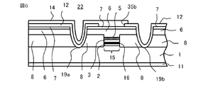
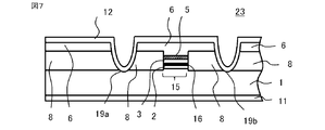
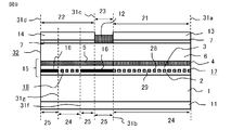
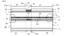
実施の形態1の半導体レーザ装置50について、図面を参照して説明する。同じ又は対応する構成要素には同じ符号を付し、説明の繰り返しを省略する場合がある。他の実施の形態においても、同じ又は対応する構成要素には同じ符号を付し、説明の繰り返しを省略する場合がある。図1は、実施の形態1に係る半導体レーザ装置を示す斜視図である。図2は図1の半導体レーザ装置における第一例のメサストライプの断面図であり、図3は図1の変調器部における回折格子を示す図である。図4は図1の半導体レーザ装置におけるレーザ部の断面図であり、図5、図6はそれぞれ図1の半導体レーザ装置における変調器部の断面図である。図7は、図1の半導体レーザ装置における分離部の断面図である。図8は図1の半導体レーザ装置における第二例のメサストライプの断面図であり、図9は図1の半導体レーザ装置における第三例のメサストライプの断面図であり、図10は図1の半導体レーザ装置における第四例のメサストライプの断面図である。図1ではレーザ光の出射方向であり光軸方向であるz方向に平行な導波路断面33も示している。図4~図7は、z方向に垂直な断面を示している。
実施の形態1の半導体レーザ装置50について、図面を参照して説明する。同じ又は対応する構成要素には同じ符号を付し、説明の繰り返しを省略する場合がある。他の実施の形態においても、同じ又は対応する構成要素には同じ符号を付し、説明の繰り返しを省略する場合がある。図1は、実施の形態1に係る半導体レーザ装置を示す斜視図である。図2は図1の半導体レーザ装置における第一例のメサストライプの断面図であり、図3は図1の変調器部における回折格子を示す図である。図4は図1の半導体レーザ装置におけるレーザ部の断面図であり、図5、図6はそれぞれ図1の半導体レーザ装置における変調器部の断面図である。図7は、図1の半導体レーザ装置における分離部の断面図である。図8は図1の半導体レーザ装置における第二例のメサストライプの断面図であり、図9は図1の半導体レーザ装置における第三例のメサストライプの断面図であり、図10は図1の半導体レーザ装置における第四例のメサストライプの断面図である。図1ではレーザ光の出射方向であり光軸方向であるz方向に平行な導波路断面33も示している。図4~図7は、z方向に垂直な断面を示している。
実施の形態1の半導体レーザ装置50は、レーザ部21、変調器部22、分離部23を備えている。レーザ部21は分布帰還型レーザが形成されている。変調器部22はn-InPの半導体基板1にモノシリックに形成された電界吸収型(EA)変調器であり、半導体レーザ装置50は電界吸収型(EA)変調器集積半導体レーザである。レーザ部21は破線31aから破線31bの間の領域に形成されており、分離部23は破線31bから破線31cの間の領域に形成されており、変調器部22は破線31cから破線31dの間の領域に形成されている。実施の形態1の半導体レーザ装置50は、分布帰還型のレーザ部21及び電界吸収型の変調器部22が同一の半導体基板1の形成されており、レーザ部21から出射されるレーザ光が変調器部22の出射端面32から出射される半導体レーザ装置である。
レーザ部21は、半導体基板1、n-InPの第一クラッド層2、回折格子17が形成された回折格子材料層16、n-InPの第二クラッド層3、活性層4、p-InPの第三クラッド層6、InP埋込層8、p-InGaAsのコンタクト層7、Si02の絶縁膜12、半導体基板1の裏面に形成されたカソード電極11、半導体基板1の表面側に形成されかつコンタクト層7に接続された第一アノード電極13を備えている。変調器部22は、半導体基板1、n-InPの第一クラッド層2、回折格子18が一部に形成された回折格子材料層16、n-InPの第二クラッド層3、吸収層5、p-InPの第三クラッド層6、InP埋込層8、p-InGaAsのコンタクト層7、Si02の絶縁膜12、半導体基板1の裏面に形成されたカソード電極11、半導体基板1の表面側に形成されかつコンタクト層7に接続された第二アノード電極14を備えている。分離部23は、レーザ部21と変調器部22とを分離する領域(分離領域、アイソレーション領域)の構造物である。分離部23は、半導体基板1、n-InPの第一クラッド層2、回折格子が形成されていない回折格子材料層16、n-InPの第二クラッド層3、吸収層5、p-InPの第三クラッド層6、InP埋込層8、Si02の絶縁膜12、半導体基板1の裏面に形成されたカソード電極11を備えている。図1において、z方向はレーザ部21が出射するレーザ光の光軸の方向であり、x方向はz方向に垂直で半導体レーザ装置50が備える各層が延伸している方向であり、y方向はx方向及びx方向に垂直で半導体レーザ装置50が備える各層が積層されている方向である。
活性層4は、InGaAsP多重量子井戸から構成されている。吸収層5は、InGaAsP多重量子井戸から構成されている。レーザ部21では、活性層4の下層すなわち半導体基板1側の第一クラッド層2と第二クラッド層3との間に、InGaAsPの回折格子材料層16に凹部29が形成された回折格子17が設けられている。変調器部22では、レーザ部21と同じInGaAsPの回折格子材料層16が形成されており、回折格子材料層16の一部に凹部29a、29b、29c、29dが形成された回折格子18が設けられている。なお、図1、図2では、レーザ部21と反対側の出射端面32の側のみに回折格子18が設けられている例を示した。分離部23にも、レーザ部21と同じInGaAsPの回折格子材料層16が形成されているが、凹部29が形成された回折格子は設けられていない。
レーザ部21に、レーザ部21が出射するレーザ光の光軸の方向(z方向)に延伸したメサであるメサストライプ15が形成されている。レーザ部21のメサストライプ15は、第一クラッド層2、回折格子17が形成された回折格子材料層16、第二クラッド層3、活性層4、第三クラッド層6の一部から構成されている。メサストライプ15を構成する第三クラッド層6の一部は、埋込層8における半導体基板1と反対側の表面位置と活性層4との間の部分である。メサストライプ15は、レーザ部21、分離部23、変調器部22に連続的に形成されている。メサストライプ15は連続的に形成されているが、レーザ部21、分離部23、変調器部22におけるメサストライプ15は、それぞれ第一メサストライプ、第三メサストライプ、第二メサストライプと区別して記載する場合もある。レーザ部21は、レーザ光の光軸の方向に延伸して形成された第一回折格子である回折格子17を備えている。
変調器部22のメサストライプ15は、第一クラッド層2、回折格子18が形成された部分を含む回折格子材料層16、第二クラッド層3、吸収層5、第三クラッド層6の一部から構成されている。分離部23のメサストライプ15は、第一クラッド層2、回折格子が形成されていない回折格子材料層16、第二クラッド層3、吸収層5、第三クラッド層6の一部から構成されている。メサストライプ15を構成する第三クラッド層6の一部は、埋込層8における半導体基板1と反対側の表面位置と吸収層5との間の部分である変調器部22は、レーザ光の光軸の方向に延伸して形成された第二回折格子である回折格子18を備えている。レーザ部21、分離部23、変調器部22のメサストライプ15におけるx方向の両側に、埋込層8、第三クラッド層6を貫通して半導体基板1に達する溝19a、19bが形成されている。なお、レーザ部21、変調器部22において、溝19a、19bはコンタクト層7も貫通している。レーザ部21、変調器部22において、絶縁膜12は、コンタクト層7及び溝19a、19bの表面に形成されている。分離部23において、絶縁膜12は、第三クラッド層6及び溝19a、19bの表面に形成されている。レーザ部21の第一アノード電極13は、絶縁膜12に形成された開口35aからコンタクト層7に接続されている。変調器部22の第二アノード電極14は、絶縁膜12に形成された開口35bからコンタクト層7に接続されている。
実施の形態1の半導体レーザ装置50は、第一クラッド層2と第二クラッド層3との間の回折格子材料層16の膜厚taが、レーザ部21、分離部23、変調器部22において同じである。図3の破線34aは回折格子材料層16の裏面(半導体基板1側の表面)を示す破線であり、破線34bは回折格子材料層16の表面(半導体基板1と反対側の表面)を示す破線である。図2に示すように、変調器部22は、メサストライプ15において、回折格子18が形成されている回折格子領域24と、回折格子18が形成されていない非回折格子領域25と、を備えている。変調器部22において、回折格子領域24は破線31fから破線31dまで領域であり、非回折格子領域25は破線31cから破線31fまでの領域である。前述したように、回折格子18は出射端面32の側に形成されており、変調器部22におけるレーザ部21の側に非回折格子領域25が設けられている。図3に示すように、回折格子18は、4つの凸部28a、28b、28c、28dと、4つの凹部29a、29b、29c、29dと、を備えている。変調器部22の凸部28a、28b、28c、28dは半導体基板1に垂直な方向に延伸しており、変調器部22の凹部29a、29b、29c、29dは変調器部22の凸部28a、28b、28c、28dの半導体基板1と反対側の面よりも半導体基板1の側に窪んでいる。図2、図3では、凸部28a、28b、28c、28dの厚さが同一であり、回折格子材料層16が削られて形成された凹部29a、29b、29c、29dの深さが、回折格子材料層16の膜厚taと同じである例を示した。なお、凸部の符号は総括的に28を用い、区別する場合に28a、28b、28c、28dを用いる。凹部の符号は総括的に29を用い、区別する場合に29a、29b、29c、29dを用いる。
図3において、破線31fと凸部28aの出射端面32側の端との間隔はzaであり、凸部28aの出射端面32側の端と凸部28bの出射端面32側の端との間隔はzbであり、凸部28bの出射端面32側の端と凸部28cの出射端面32側の端との間隔はzcであり、凸部28cの出射端面32側の端と凸部28dの出射端面32側の端との間隔はzdである。なお、凸部28dの出射端面32側の端と出射端面32とは一致している。間隔za、間隔zb、間隔zc、間隔zdは、隣接している一組の凸部28及び凹部29の間隔であり、それらは同じである。図3では、凸部28のz方向の幅と凹部29のz方向の幅とが同じ例を示した。実施の形態1の回折格子18は、凸部28及び凹部29の周期が回折格子全体に亘って同じである。すなわち、実施の形態1の回折格子18は、凸部28及び凹部29の周期が均一である。
レーザ部21は、メサストライプ15において、z方向の全体に亘ってすなわち破線31aから破線31bの間に、回折格子17が形成されている。つまり、レーザ部21は、メサストライプ15において、回折格子が形成されていない非回折格子領域25はなく、全て回折格子が形成された回折格子領域24のみである。また、レーザ部21の回折格子17は、複数の凸部28と複数の凹部29を備えている。レーザ部21の凸部28は半導体基板1に垂直な方向に延伸しており、レーザ部21の凹部29はレーザ部21の凸部28の半導体基板1と反対側の面よりも半導体基板1の側に窪んでいる。図2では、回折格子材料層16が削られて形成された凹部29の深さが、回折格子材料層16の膜厚taと同じ例を示した。レーザ部21の回折格子17における隣接している一組の凸部28及び凹部29の間隔は、変調器部22の回折格子18における隣接している一組の凸部28及び凹部29の間隔と同じである。実施の形態1の回折格子17は、凸部28及び凹部29の周期が回折格子全体に亘って同じである。すなわち、実施の形態1の回折格子17は、凸部28及び凹部29の周期が均一である。
分離部23は、z方向の全体に亘ってすなわち破線31bから破線31cの間に、回折格子が形成されていない。つまり、分離部23は、メサストライプ15において、回折格子が形成された回折格子領域24はなく、全て回折格子が形成されていない非回折格子領域25のみである。図2に示した半導体レーザ装置50は、変調器部22の回折格子18とレーザ光が変調器部22に出射されるレーザ部21の出射端(破線31bで示す端部)との間に、回折格子が形成されていない非回折格子領域25が介在している、半導体レーザ装置である。
半導体レーザ装置50の製造方法を説明する。半導体基板1の表面に第一クラッド層2、回折格子材料層16をMOCVD(Metal organic chemical vapor deposition)法で順次結晶成長し、回折格子材料層16に凹部29を形成して回折格子17、18を形成する。回折格子17、18を含む回折格子材料層16の表面に、第二クラッド層3、活性層4及び吸収層5、第三クラッド層6の一部をMOCVD法で順次結晶成長し、SiO2のマスクを用いてメサストライプ15をドライエッチングで形成する。その後、メサストライプ15の両側の露出した半導体基板1に埋込層8を結晶成長する。
SiO2のマスクを除去し、埋込層8及びメサストライプ15の表面に第三クラッド層6、コンタクト層7を順次結晶成長し、フォトレジストのマスクを用いたウェットエッチングにて、分離部23の表面のコンタクト層7を除去する。フォトレジストのマスクの除去後、フォトレジストのマスクを用いたウェットエッチングにて、溝19a、19bを形成する。フォトレジストのマスクを除去し、分離部23の第三クラッド層6、コンタクト層7及び溝19a、19bの表面に絶縁膜12を形成する。フォトレジストのマスクを用いて絶縁膜12の開口35a、35bを形成する。フォトレジストのマスクを除去し、半導体レーザ装置50の表面及び裏面に金属層を成膜し、カソード電極11、第一アノード電極13、第二アノード電極14を形成する。その後、第一アノード電極13と第二アノード電極14の間に絶縁膜12を厚く形成する。
EA変調器と分布帰還型レーザとが集積され、かつEA変調器の領域に回折格子が形成されていない半導体レーザ装置(比較例の半導体レーザ装置)では、レーザ光の出射端面(変調器部側の端面)からの反射光が分布帰還型レーザに入射することで、分布帰還型レーザの発振波長が変動する断熱チャープが発生する。また、この断熱チャープは、光信号が光ファイバ内を伝送した際の伝送特性に影響を与える。比較例の半導体レーザ装置は、EA変調器の領域に回折格子が形成されていないので、レーザ光の出射端面(変調器部側の端面)にて反射した戻り光である反射光の位相が出射端面の劈開位置により半導体レーザ装置毎に変化する。これに対して、実施の形態1の半導体レーザ装置50は、変調器部22に回折格子18を設けている。このため、実施の形態1の半導体レーザ装置50は、半導体レーザ装置50の素子前方すなわち出射端面32で発生するレーザ光の反射光の位相が変調器部の回折格子18のレーザ部21側の開始位置等の構造で決まるため、半導体レーザ装置毎に素子前方からの反射光の位相がばらついている半導体レーザ装置毎の位相ばらつきを大きく抑制可能である。その結果、実施の形態1の半導体レーザ装置50は、半導体レーザ装置毎の断熱チャープ量のばらつきが抑制でき、伝送歩留の低下を避けることが可能である。
また、実施の形態1の半導体レーザ装置50は、変調器部22の前方すなわち出射端面32の側に、回折格子を備えた導波路を付加する必要がない。このため、実施の形態1の半導体レーザ装置50は、回折格子を備えた導波路を付加する構造の半導体レーザ装置に比べて、製造プロセスが容易であり、素子サイズも小さいため、コスト低減が可能となる。
特許文献1の半導体レーザ装置では、EA変調器領域の導波路の全体に回折格子が形成されており、更に変調器電極とレーザ電極とが分離されている分離領域にも回折格子が形成されている。回折格子では光の反射が生じるので、回折格子の領域が大きくなると、半導体レーザ装置からのレーザ光の光出力が低下する問題がある。これに対して、実施の形態1の半導体レーザ装置50は、図2、図3のように変調器部22のレーザ部21の側及び分離部23に回折格子が形成されておらず、すなわち少なくとも分離部23に回折格子が形成されていないので、特許文献1の半導体レーザ装置に比べて、レーザ光の光出力を大きくすることが可能である。
今まで、変調器部22の出射端面32の側に回折格子18が形成された半導体レーザ装置50の例を説明したが、回折格子18の配置例はこれに限定されない。回折格子18はレーザ部21のレーザ光が出射される端(出射端)すなわち破線31bで示した端から変調器部22に形成された回折格子18までの間に非回折格子領域25が介在されていればよい。この場合でも、レーザ部21から出射端面32までの間に回折格子18が形成されていない非回折格子領域25が存在するので、分布帰還型レーザ領域のレーザ光が出射される出射端からEA変調器領域の出射端に至るまで回折格子が形成されている特許文献1の半導体レーザ装置に比べて、レーザ光の光出力を大きくすることができる。図8に示した第二例のメサストライプ15を備えた半導体レーザ装置50は、変調器部22のメサストライプ15において、レーザ部21の側に回折格子18が形成された例である。図8に示した第二例のメサストライプ15の変調器部22及び分離部23では、破線31cから破線31fの間は回折格子18が形成された回折格子領域24であり、破線31fから破線31dの間及び破線31bから破線31cの間は回折格子18が形成されていない非回折格子領域25である。
図9に示した第三例のメサストライプ15を備えた半導体レーザ装置50は、変調器部22のメサストライプ15において、中央部に回折格子18が形成された例である。図9に示した第三例のメサストライプ15の変調器部22及び分離部23では、破線31fから破線31gの間は回折格子18が形成された回折格子領域24であり、破線31bから破線31fの間及び破線31gから破線31dの間は回折格子18が形成されていない非回折格子領域25である。図10に示した第四例のメサストライプ15を備えた半導体レーザ装置50は、変調器部22のメサストライプ15における全体に回折格子18が形成された例である。図10に示した第四例のメサストライプ15を備えた半導体レーザ装置50でも、メサストライプ15において、レーザ部21の出射端から出射端面32までの間に回折格子18が形成されていない非回折格子領域25が存在するので、分布帰還型レーザ領域のレーザ光が出射される出射端からEA変調器領域の出射端に至るまで回折格子が形成されている特許文献1の半導体レーザ装置に比べて、レーザ光の光出力を大きくすることができる。
なお、レーザ部21と変調器部22との間に分離部23が形成されている例で説明した。しかし、分離部23が形成されていない半導体レーザ装置50であっても、メサストライプ15において、レーザ部21の出射端から出射端面32までの間に回折格子18が形成されていない非回折格子領域25が存在する構造であればよい。この場合でも、メサストライプ15において、レーザ部21の出射端から出射端面32までの間に回折格子18が形成されていない非回折格子領域25が存在するので、分布帰還型レーザ領域のレーザ光が出射される出射端からEA変調器領域の出射端に至るまで回折格子が形成されている特許文献1の半導体レーザ装置に比べて、レーザ光の光出力を大きくすることができる。レーザ部21と変調器部22との間に分離部23が形成されていない半導体レーザ装置50は、例えば、特許文献1の半導体レーザ装置と同様にコンタクト層7をレーザ部21と変調器部22とで分離しないようにした装置である(分離部なしの第一例)。また、レーザ部21と変調器部22との間に分離部23が形成されていない半導体レーザ装置50は、レーザ部21と変調器部22との間に段差を設けて、レーザ部21のコンタクト層7及び第一アノード電極13と変調器部22のコンタクト層7及び第二アノード電極14とを分離するようにした装置である(分離部なしの第二例)。なお、分離部なしの第一例、分離部なしの第二例の場合は、図10に示した第四例のメサストライプ15の構造は適用できない。
以上のように、実施の形態1の半導体レーザ装置50は、分布帰還型のレーザ部21及び電界吸収型の変調器部22が同一の半導体基板1に形成されており、レーザ部21から出射されるレーザ光が変調器部22の出射端面32から出射される半導体レーザ装置である。実施の形態1の半導体レーザ装置50は、レーザ部21が、レーザ光の光軸の方向に延伸して形成された第一回折格子(回折格子17)を備え、変調器部22が、少なくとも一部にレーザ光の光軸の方向に延伸して形成された第二回折格子(回折格子18)を備えている。実施の形態1の半導体レーザ装置50は、変調器部22の第二回折格子(回折格子18)とレーザ光が変調器部22に出射されるレーザ部21の出射端(破線31bで示す端部)との間に、回折格子が形成されていない非回折格子領域25が介在している。実施の形態1の半導体レーザ装置50は、この構成により、変調器部22の第二回折格子(回折格子18)とレーザ光が変調器部22に出射されるレーザ部21の出射端(破線31bで示す端部)との間に、回折格子が形成されていない非回折格子領域25が介在しているので、レーザ光の光出力を増加させることができる。
実施の形態2.
図11は実施の形態2に係る半導体レーザ装置を示す斜視図であり、図12は図11の半導体レーザ装置におけるメサストライプの断面図である。図13は図11の変調器部における回折格子を示す図であり、図14は図11の半導体レーザ装置における変調器部の断面図である。実施の形態2の半導体レーザ装置50は、変調器部22の回折格子領域24に周期が不均一な回折格子26が形成されている点で、実施の形態1の半導体レーザ装置50と異なる。実施の形態1の半導体レーザ装置50と異なる部分を主に説明する。
図11は実施の形態2に係る半導体レーザ装置を示す斜視図であり、図12は図11の半導体レーザ装置におけるメサストライプの断面図である。図13は図11の変調器部における回折格子を示す図であり、図14は図11の半導体レーザ装置における変調器部の断面図である。実施の形態2の半導体レーザ装置50は、変調器部22の回折格子領域24に周期が不均一な回折格子26が形成されている点で、実施の形態1の半導体レーザ装置50と異なる。実施の形態1の半導体レーザ装置50と異なる部分を主に説明する。
図13に示すように、回折格子26は、4つの凸部28a、28b、28c、28dと、4つの凹部29a、29b、29c、29dと、を備えている。図12、図13では、回折格子材料層16が削られて形成された凹部29a、29b、29c、29dの深さが、回折格子材料層16の膜厚taと同じ例を示した。なお、凸部の符号は総括的に28を用い、区別する場合に28a、28b、28c、28dを用いる。凹部の符号は総括的に29を用い、区別する場合に29a、29b、29c、29dを用いる。
図13において、破線31fと凸部28aの出射端面32側の端との間隔はzaであり、凸部28aの出射端面32側の端と凸部28bの出射端面32側の端との間隔はzbであり、凸部28bの出射端面32側の端と凸部28cの出射端面32側の端との間隔はzcであり、凸部28cの出射端面32側の端と凸部28dの出射端面32側の端との間隔はzdである。なお、凸部28dの出射端面32側の端と出射端面32とは一致している。間隔za、間隔zb、間隔zc、間隔zdは、隣接している一組の凸部28及び凹部29の間隔であり、それらは異なっている。図13では、間隔za、zb、zc、zdは、式(1)の関係になっており、凸部28のz方向の幅と凹部29のz方向の幅とが同じ例を示した。
zd>zc>zb>za ・・・(1)
zd>zc>zb>za ・・・(1)
実施の形態2の回折格子26は、凸部28及び凹部29の間隔がレーザ光の出射方向であるz方向に対して不均一である。すなわち、実施の形態2の回折格子26は、凸部28及び凹部29の周期が不均一である。
回折格子では、どの波長の光が反射するかは、回折格子の周期に依存する。従って、回折格子の周期を不均一とした実施の形態2の回折格子26では、変調器部22の回折格子26で生じる光反射の波長帯域を、均一周期の回折格子である場合に比べ、拡大することができる。すなわち、変調器部22において不均一周期の回折格子26を備えた実施の形態2の半導体レーザ装置50は、変調器部22において均一周期の回折格子18を備えた実施の形態1の半導体レーザ装置50に比べ、回折格子で生じる光反射の波長帯域を拡大することができる。これにより、実施の形態2の半導体レーザ装置50は、レーザ部21又は及び変調器部22の駆動条件が変化した場合、又は製造ばらつきにより半導体レーザ装置50の素子サイズが変化した場合でも、レーザ部21から発生する出力光を、変調器部22の回折格子26により確実にレーザ部21側に反射させることが可能となる。すなわち、実施の形態2の半導体レーザ装置50は、半導体レーザ装置毎の断熱チャープ量のばらつきが抑制でき、伝送歩留の低下を避けることが可能であるという実施の形態1の半導体レーザ装置50の効果が、実施の形態1の半導体レーザ装置50よりも駆動条件が変化した場合、製造ばらつきが生じた場合の一方又は両方の場合でも、得られるようになる。つまり、実施の形態2の半導体レーザ装置50は、実施の形態1の半導体レーザ装置50よりも駆動条件の変化及び製造ばらつきに対する耐性が強化されている。
実施の形態2の半導体レーザ装置50は、変調器部22の回折格子の周期以外の構造が実施の形態1の半導体レーザ装置50と同じである。このため、実施の形態2の半導体レーザ装置50は、実施の形態1の半導体レーザ装置50と同様に、少なくとも分離部23に回折格子26が形成されていない構造又はレーザ部21の出射端から出射端面32までの間に回折格子26が形成されていない非回折格子領域25が存在する構造を有しているので、特許文献1の半導体レーザ装置に比べて、レーザ光の光出力を大きくすることが可能である。
実施の形態2の半導体レーザ装置50は、変調器部22のメサストライプ15において不均一周期の回折格子26を備えているので、半導体レーザ装置50の素子前方すなわち出射端面32で発生する反射光が、光反射の波長帯域が広がっている変調器部22の回折格子26により吸収層5及び活性層4から離れた位置へ向かうので、素子前方からの反射光がレーザ部21の活性層4に伝搬することを抑制でき、半導体レーザ装置毎の断熱チャープ量のばらつきが抑制でき、伝送歩留の低下を避けることが可能である。
また、実施の形態2の半導体レーザ装置50は、実施の形態1の半導体レーザ装置50と同様に、変調器部22の前方すなわち出射端面32の側に、回折格子を備えた導波路を付加する必要がない。このため、実施の形態2の半導体レーザ装置50は、回折格子を備えた導波路を付加する構造の半導体レーザ装置に比べて、製造プロセスが容易であり、素子サイズも小さいため、コスト低減が可能となる。
実施の形態3.
図15は実施の形態3に係る半導体レーザ装置を示す斜視図であり、図16は図15の変調器部における第一例の回折格子を示す図であり、図17は図15の半導体レーザ装置における変調器部の断面図である。図18は図15の変調器部における第二例の回折格子を示す図であり、図19は図15の変調器部における第三例の回折格子を示す図である。実施の形態3の半導体レーザ装置50は、変調器部22の回折格子領域24に凹部29の深さ又は及び凸部28の厚さが不均一な回折格子27が形成されている点で、実施の形態1の半導体レーザ装置50と異なる。実施の形態1の半導体レーザ装置50と異なる部分を主に説明する。
図15は実施の形態3に係る半導体レーザ装置を示す斜視図であり、図16は図15の変調器部における第一例の回折格子を示す図であり、図17は図15の半導体レーザ装置における変調器部の断面図である。図18は図15の変調器部における第二例の回折格子を示す図であり、図19は図15の変調器部における第三例の回折格子を示す図である。実施の形態3の半導体レーザ装置50は、変調器部22の回折格子領域24に凹部29の深さ又は及び凸部28の厚さが不均一な回折格子27が形成されている点で、実施の形態1の半導体レーザ装置50と異なる。実施の形態1の半導体レーザ装置50と異なる部分を主に説明する。
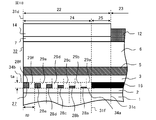
図16に示すように、回折格子27は、6つの凸部28a、28b、28c、28d、28e、28fと、6つの凹部29a、29b、29c、29d、29e、29fと、を備えている。なお、凸部の符号は総括的に28を用い、区別する場合に28a、28b、28c、28d、28e、28fを用いる。凹部の符号は総括的に29を用い、区別する場合に29a、29b、29c、29d、29e、29fを用いる。図16では、凸部28が回折格子材料層16の膜厚taと同じあり、回折格子材料層16が削られて形成された凹部29a、29b、29c、29d、29e、29fの深さが、同一でない例を示した。すなわち、図16に示した変調器部22における第一例の回折格子27は、凸部28の厚さが均一であり、回折格子材料層16が削られて形成された凹部29の深さが不均一である例である。
図16において、破線31fと凸部28aの出射端面32側の端との間隔は、凸部28eの出射端面32側の端と凸部28fの出射端面32側の端との間隔と同じく、zpである。なお、凸部28fの出射端面32側の端と出射端面32とは一致している。また、凸部28aの出射端面32側の端と凸部28bの出射端面32側の端との間隔、凸部28bの出射端面32側の端と凸部28cの出射端面32側の端との間隔、凸部28cの出射端面32側の端と凸部28dの出射端面32側の端との間隔、凸部28dの出射端面32側の端と凸部28eの出射端面32側の端との間隔は、それぞれzpである。間隔zpは、隣接している一組の凸部28及び凹部29の間隔であり、それらは同じである。図16では、凸部28のz方向の幅と凹部29のz方向の幅とが同じ例を示した。実施の形態3の回折格子27は、凸部28及び凹部29の周期が回折格子全体に亘って同じである。すなわち、実施の形態3の回折格子27は、凸部28及び凹部29の周期が均一である。しかし、実施の形態3の回折格子27は、前述したように変調器部22の回折格子領域24に凹部29の深さ又は及び凸部28の厚さが不均一である。
回折格子の溝すなわち凹部29の深さ又は及び、溝未形成部すなわち凸部28の厚さを変化させると、回折格子の等価屈折率が変化する。等価屈折率がz方向に対して不均一な回折格子は、均一の等価屈折率の回折格子に比べ、回折格子の光反射の波長帯域が拡大する。すなわち、変調器部22において等価屈折率がz方向に対して不均一な回折格子27を備えた実施の形態3の半導体レーザ装置50は、変調器部22において等価屈折率がz方向に対して均一な回折格子18を備えた実施の形態1の半導体レーザ装置50に比べ、回折格子で生じる光反射の波長帯域を拡大することができる。これにより、実施の形態3の半導体レーザ装置50は、レーザ部21又は及び変調器部22の駆動条件が変化した場合、又は製造ばらつきにより半導体レーザ装置50の素子サイズが変化した場合でも、レーザ部21から発生する出力光を、変調器部22の回折格子27により確実にレーザ部21側に反射させることが可能となる。すなわち、実施の形態3の半導体レーザ装置50は、半導体レーザ装置毎の断熱チャープ量のばらつきが抑制でき、伝送歩留の低下を避けることが可能であるという実施の形態1の半導体レーザ装置50の効果が、実施の形態1の半導体レーザ装置50よりも駆動条件が変化した場合、製造ばらつきが生じた場合の一方又は両方の場合でも、得られるようになる。つまり、実施の形態3の半導体レーザ装置50は、実施の形態1の半導体レーザ装置50よりも駆動条件の変化及び製造ばらつきに対する耐性が強化されている。
実施の形態3の半導体レーザ装置50は、変調器部22の回折格子以外の構造が実施の形態1の半導体レーザ装置50と同じである。このため、実施の形態3の半導体レーザ装置50は、実施の形態1の半導体レーザ装置50と同様に、少なくとも分離部23に回折格子27が形成されていない構造又はレーザ部21の出射端から出射端面32までの間に回折格子27が形成されていない非回折格子領域25が存在する構造を有しているので、特許文献1の半導体レーザ装置に比べて、レーザ光の光出力を大きくすることが可能である。
実施の形態3の半導体レーザ装置50は、変調器部22のメサストライプ15において等価屈折率がz方向に対して不均一な回折格子27を備えているので、半導体レーザ装置50の素子前方すなわち出射端面32で発生する反射光が、光反射の波長帯域が広がっている変調器部22の回折格子27により吸収層5及び活性層4から離れた位置へ向かうので、素子前方からの反射光がレーザ部21の活性層4に伝搬することを抑制でき、半導体レーザ装置毎の断熱チャープ量のばらつきが抑制でき、伝送歩留の低下を避けることが可能である。
また、実施の形態3の半導体レーザ装置50は、実施の形態1の半導体レーザ装置50と同様に、変調器部22の前方すなわち出射端面32の側に、回折格子を備えた導波路を付加する必要がない。このため、実施の形態3の半導体レーザ装置50は、回折格子を備えた導波路を付加する構造の半導体レーザ装置に比べて、製造プロセスが容易であり、素子サイズも小さいため、コスト低減が可能となる。
等価屈折率がz方向に対して不均一な回折格子27は、図16の構造に限定されない。図18に示した変調器部22における第二例の回折格子27のように、凸部28の厚さが不均一であり、回折格子材料層16が削られて形成された凹部29の深さが均一であってもよい。また、図19に示した変調器部22における第三例の回折格子27のように、凸部28の厚さが不均一であり、かつ回折格子材料層16が削られて形成された凹部29の深さが不均一であってもよい。図18では、z方向の正方向に向かって、凸部28の厚さが増加しており、凹部29の深さが均一である例を示した。図19では、2つの凸部28の組の厚さがz方向の正側に向かって増加しており、2つの凹部29の組が深い凹部と浅い凹部を有している例を示した。
凸部28a、28b、28c、28d、28e、28fの厚さをそれぞれ、ha、hb、hc、hd、he、hfとし、凹部29a、29b、29c、29d、29e、29fの深さをそれぞれ、da、db、dc、dd、de、dfとする。凸部28の厚さは、破線34aに対するy方向の正側(図18、図19において上側)の厚さである。凹部29の深さは、破線34bに対するy方向の負側(図18、図19において下側)の深さである。図18に示した変調器部22における第二例の回折格子27は、式(2)及び式(3)が成立しており、図19に示した変調器部22における第三例の回折格子27は、式(4)及び式(5)が成立している。
hf>he>hd>hc>hb>ha ・・・(2)
df=de=dd=dc=db=da ・・・(3)
(hf=he)>(hd=hc)>(hb=ha) ・・・(4)
(df=dd=db)<(de=dc=da) ・・・(5)
なお、式(4)、式(5)において、等しい厚さ又は深さを()で括り、()毎の大小関係を明確にした。
df=de=dd=dc=db=da ・・・(3)
(hf=he)>(hd=hc)>(hb=ha) ・・・(4)
(df=dd=db)<(de=dc=da) ・・・(5)
なお、式(4)、式(5)において、等しい厚さ又は深さを()で括り、()毎の大小関係を明確にした。
図18、図19において、図16と同様に、破線31fと凸部28aの出射端面32側の端との間隔は、凸部28eの出射端面32側の端と凸部28fの出射端面32側の端との間隔と同じく、zpである。なお、凸部28fの出射端面32側の端と出射端面32とは一致している。また、凸部28aの出射端面32側の端と凸部28bの出射端面32側の端との間隔、凸部28bの出射端面32側の端と凸部28cの出射端面32側の端との間隔、凸部28cの出射端面32側の端と凸部28dの出射端面32側の端との間隔、凸部28dの出射端面32側の端と凸部28eの出射端面32側の端との間隔は、それぞれzpである。間隔zpは、隣接している一組の凸部28及び凹部29の間隔であり、それらは同じである。図18、図19では、凸部28のz方向の幅と凹部29のz方向の幅とが同じ例を示した。
なお、本願は、様々な例示的な実施の形態及び実施例が記載されているが、1つ、または複数の実施の形態に記載された様々な特徴、態様、及び機能は特定の実施の形態の適用に限られるのではなく、単独で、または様々な組み合わせで実施の形態に適用可能である。従って、例示されていない無数の変形例が、本願明細書に開示される技術の範囲内において想定される。例えば、少なくとも1つの構成要素を変形する場合、追加する場合または省略する場合、さらには、少なくとも1つの構成要素を抽出し、他の実施の形態の構成要素と組み合わせる場合が含まれるものとする。
1…半導体基板、4…活性層、5…吸収層、11…カソード電極、13…第一アノード電極、14…第二アノード電極、15…メサストライプ、16…回折格子材料層、17…回折格子、18…回折格子、21…レーザ部、22…変調器部、23…分離部、25…非回折格子領域、26…回折格子、27…回折格子、28、28a、28b、28c、28d、28e、28f…凸部、29、29a、29b、29c、29d、29e、29f…凹部、32…出射端面、50…半導体レーザ装置、za、zb、zc、zd…間隔
Claims (13)
- 分布帰還型のレーザ部及び電界吸収型の変調器部が同一の半導体基板に形成されており、前記レーザ部から出射されるレーザ光が前記変調器部の出射端面から出射される半導体レーザ装置であって、
前記レーザ部は、前記レーザ光の光軸の方向に延伸して形成された第一回折格子を備え、
前記変調器部は、少なくとも一部に前記レーザ光の光軸の方向に延伸して形成された第二回折格子を備え、
前記変調器部の前記第二回折格子と前記レーザ光が前記変調器部に出射される前記レーザ部の出射端との間に、回折格子が形成されていない非回折格子領域が介在している、半導体レーザ装置。 - 前記第一回折格子は、前記半導体基板に垂直な方向に延伸した複数の第一凸部と、前記第一凸部の前記半導体基板と反対側の面よりも前記半導体基板の側に窪んでいる複数の第一凹部と、を備え、
前記第二回折格子は、前記半導体基板に垂直な方向に延伸した複数の第二凸部と、前記第二凸部の前記半導体基板と反対側の面よりも前記半導体基板の側に窪んでいる複数の第二凹部と、を備え、
前記第二回折格子の前記第二凹部は、前記半導体基板に垂直な方向の深さが前記第一回折格子の前記第一凹部と同じである、請求項1記載の半導体レーザ装置。 - 前記第二回折格子は、隣接している一組の前記第二凸部及び前記第二凹部における前記レーザ光の光軸の方向の間隔が均一である、請求項2記載の半導体レーザ装置。
- 前記第二回折格子は、隣接している一組の前記第二凸部及び前記第二凹部における前記レーザ光の光軸の方向の間隔が不均一である、請求項2記載の半導体レーザ装置。
- 前記第二回折格子は、前記第二凸部における前記半導体基板に垂直な方向の厚さが不均一である、請求項2から4のいずれか1項に記載の半導体レーザ装置。
- 前記第一回折格子は、前記半導体基板に垂直な方向に延伸した複数の第一凸部と、前記第一凸部の前記半導体基板と反対側の面よりも前記半導体基板の側に窪んでいる複数の第一凹部と、を備え、
前記第二回折格子は、前記半導体基板に垂直な方向に延伸した複数の第二凸部と、前記第二凸部の前記半導体基板と反対側の面よりも前記半導体基板の側に窪んでいる複数の第二凹部と、を備え、
前記第二回折格子は、前記第二凹部における前記半導体基板に垂直な方向の深さが不均一である、請求項1記載の半導体レーザ装置。 - 前記第二回折格子は、隣接している一組の前記第二凸部及び前記第二凹部における前記レーザ光の光軸の方向の間隔が均一である、請求項6記載の半導体レーザ装置。
- 前記第二回折格子は、隣接している一組の前記第二凸部及び前記第二凹部における前記レーザ光の光軸の方向の間隔が不均一である、請求項6記載の半導体レーザ装置。
- 前記第二回折格子は、前記第二凸部における前記半導体基板に垂直な方向の厚さが不均一である、請求項6から8のいずれか1項に記載の半導体レーザ装置。
- 前記第二回折格子は、前記第一回折格子と同一の回折格子材料層により形成されている請求項1から請求項9のいずれか1項に記載の半導体レーザ装置。
- 前記変調器部における前記レーザ部の側に、前記非回折格子領域が設けられている、請求項1から請求項10のいずれか1項に記載の半導体レーザ装置。
- 前記半導体基板の裏面に形成されたカソード電極と、前記半導体基板の表面側に形成された前記変調器部のアノード電極及び前記レーザ部のアノード電極と、を備え、
前記変調器部と前記レーザ部の前記出射端との間に、前記変調器部のアノード電極と前記レーザ部のアノード電極とが分離された分離部が設けられている、請求項1から請求項11のいずれか1項に記載の半導体レーザ装置。 - 前記レーザ部は、活性層及び前記第一回折格子を含むと共に、前記レーザ光の光軸の方向に延伸して形成されたメサである第一メサストライプを備え、
前記変調器部は、吸収層及び前記第二回折格子を含むと共に、前記レーザ光の光軸の方向に延伸して形成されたメサである第二メサストライプを備え、
前記変調器部における前記レーザ部の側の端部と前記レーザ光が前記変調器部に出射される前記レーザ部の出射端との間に設けられた前記非回折格子領域は、前記変調器部の前記吸収層及び前記レーザ部の前記活性層に接続された吸収層を含むと共に、前記レーザ光の光軸の方向に延伸して形成されたメサである第三メサストライプを備え、
前記第一メサストライプ、前記第二メサストライプ、前記第三メサストライプは連続している、請求項1から請求項12のいずれか1項に記載の半導体レーザ装置。
Priority Applications (4)
| Application Number | Priority Date | Filing Date | Title |
|---|---|---|---|
| CN201980098685.9A CN114175427B (zh) | 2019-08-02 | 2019-08-02 | 半导体激光器装置 |
| US17/595,482 US20220231478A1 (en) | 2019-08-02 | 2019-08-02 | Semiconductor laser device |
| JP2019571767A JP6671573B1 (ja) | 2019-08-02 | 2019-08-02 | 半導体レーザ装置 |
| PCT/JP2019/030401 WO2021024288A1 (ja) | 2019-08-02 | 2019-08-02 | 半導体レーザ装置 |
Applications Claiming Priority (1)
| Application Number | Priority Date | Filing Date | Title |
|---|---|---|---|
| PCT/JP2019/030401 WO2021024288A1 (ja) | 2019-08-02 | 2019-08-02 | 半導体レーザ装置 |
Publications (1)
| Publication Number | Publication Date |
|---|---|
| WO2021024288A1 true WO2021024288A1 (ja) | 2021-02-11 |
Family
ID=70000815
Family Applications (1)
| Application Number | Title | Priority Date | Filing Date |
|---|---|---|---|
| PCT/JP2019/030401 Ceased WO2021024288A1 (ja) | 2019-08-02 | 2019-08-02 | 半導体レーザ装置 |
Country Status (4)
| Country | Link |
|---|---|
| US (1) | US20220231478A1 (ja) |
| JP (1) | JP6671573B1 (ja) |
| CN (1) | CN114175427B (ja) |
| WO (1) | WO2021024288A1 (ja) |
Cited By (1)
| Publication number | Priority date | Publication date | Assignee | Title |
|---|---|---|---|---|
| JP2023020996A (ja) * | 2021-07-28 | 2023-02-09 | 日本電信電話株式会社 | 半導体光デバイス |
Families Citing this family (1)
| Publication number | Priority date | Publication date | Assignee | Title |
|---|---|---|---|---|
| JP7397376B2 (ja) * | 2020-07-02 | 2023-12-13 | 日本電信電話株式会社 | 光送信器 |
Citations (5)
| Publication number | Priority date | Publication date | Assignee | Title |
|---|---|---|---|---|
| JPH04198913A (ja) * | 1990-11-29 | 1992-07-20 | Fujitsu Ltd | 電界吸収型半導体光変調器 |
| WO2002075880A1 (en) * | 2001-03-15 | 2002-09-26 | Corning Lasertron Incorporated | Electroabsorption modulated laser |
| JP2003069135A (ja) * | 2001-08-28 | 2003-03-07 | Fujitsu Ltd | 光半導体装置 |
| JP2009260192A (ja) * | 2008-04-21 | 2009-11-05 | Sumitomo Electric Ind Ltd | 半導体光集積素子及びその製造方法 |
| JP2018067604A (ja) * | 2016-10-18 | 2018-04-26 | 三菱電機株式会社 | 光変調器付き半導体レーザ装置 |
Family Cites Families (7)
| Publication number | Priority date | Publication date | Assignee | Title |
|---|---|---|---|---|
| JP2001320124A (ja) * | 2000-05-09 | 2001-11-16 | Nec Corp | 変調器集積化光源及び光通信用モジュール |
| GB2437784B (en) * | 2006-05-02 | 2011-05-11 | Jian-Jun He | Q-modulated semiconductor laser with electro-absorptive grating structures |
| CN100377453C (zh) * | 2006-05-12 | 2008-03-26 | 何建军 | 带有电吸收光栅结构的q-调制半导体激光器 |
| JP2008294124A (ja) * | 2007-05-23 | 2008-12-04 | Fujitsu Ltd | 光半導体素子 |
| JP6275841B2 (ja) * | 2013-12-27 | 2018-02-07 | インテル・コーポレーション | 非対称光導波路格子共振器及びdbrレーザ |
| JP6388007B2 (ja) * | 2016-08-08 | 2018-09-12 | 三菱電機株式会社 | 光デバイスの製造方法 |
| CN107611772B (zh) * | 2017-09-25 | 2020-07-28 | 清华大学 | 电吸收调制激光器及其制备方法 |
-
2019
- 2019-08-02 JP JP2019571767A patent/JP6671573B1/ja active Active
- 2019-08-02 CN CN201980098685.9A patent/CN114175427B/zh active Active
- 2019-08-02 WO PCT/JP2019/030401 patent/WO2021024288A1/ja not_active Ceased
- 2019-08-02 US US17/595,482 patent/US20220231478A1/en active Pending
Patent Citations (5)
| Publication number | Priority date | Publication date | Assignee | Title |
|---|---|---|---|---|
| JPH04198913A (ja) * | 1990-11-29 | 1992-07-20 | Fujitsu Ltd | 電界吸収型半導体光変調器 |
| WO2002075880A1 (en) * | 2001-03-15 | 2002-09-26 | Corning Lasertron Incorporated | Electroabsorption modulated laser |
| JP2003069135A (ja) * | 2001-08-28 | 2003-03-07 | Fujitsu Ltd | 光半導体装置 |
| JP2009260192A (ja) * | 2008-04-21 | 2009-11-05 | Sumitomo Electric Ind Ltd | 半導体光集積素子及びその製造方法 |
| JP2018067604A (ja) * | 2016-10-18 | 2018-04-26 | 三菱電機株式会社 | 光変調器付き半導体レーザ装置 |
Cited By (2)
| Publication number | Priority date | Publication date | Assignee | Title |
|---|---|---|---|---|
| JP2023020996A (ja) * | 2021-07-28 | 2023-02-09 | 日本電信電話株式会社 | 半導体光デバイス |
| JP7723237B2 (ja) | 2021-07-28 | 2025-08-14 | Ntt株式会社 | 半導体光デバイス |
Also Published As
| Publication number | Publication date |
|---|---|
| CN114175427A (zh) | 2022-03-11 |
| US20220231478A1 (en) | 2022-07-21 |
| CN114175427B (zh) | 2024-04-19 |
| JPWO2021024288A1 (ja) | 2021-09-13 |
| JP6671573B1 (ja) | 2020-03-25 |
Similar Documents
| Publication | Publication Date | Title |
|---|---|---|
| JP5177285B2 (ja) | 光素子及びその製造方法 | |
| JPS61216383A (ja) | 分布帰還型半導体レ−ザ | |
| US20170146734A1 (en) | Semiconductor optical integrated device and method of manufacturing the same | |
| GB2416427A (en) | DFB laser | |
| JP2982422B2 (ja) | 半導体レーザおよびその製造方法 | |
| JP6510391B2 (ja) | 半導体レーザ | |
| JP6717733B2 (ja) | 半導体光集積回路 | |
| JP6588859B2 (ja) | 半導体レーザ | |
| WO2021024288A1 (ja) | 半導体レーザ装置 | |
| US20020064203A1 (en) | Strip-loaded tunable distributed feedback laser | |
| JP6588858B2 (ja) | 半導体レーザ | |
| US6567446B1 (en) | Optical device with increased spectral width | |
| EP3970246B1 (en) | Optical device with passive window | |
| US20170194766A1 (en) | Optical device and optical module | |
| EP4311042B1 (en) | Opto-electronic device | |
| US10680409B2 (en) | Laser device | |
| US7548574B2 (en) | Integrated modulator/laser assembly and a method of producing same | |
| JP5092928B2 (ja) | 光半導体装置 | |
| JP2000277851A (ja) | 分布帰還型半導体レーザ | |
| JP2024547119A5 (ja) | ||
| JP2000049417A (ja) | 半導体発光素子およびその素子を組み込んだ半導体発光装置ならびにそれらの製造方法 | |
| JP2013160873A (ja) | 光導波路、光導波路を含むレーザ、光導波路を含むモジュール、光導波路の製造方法 | |
| JP3773880B2 (ja) | 分布帰還型半導体レーザ | |
| JPS63213383A (ja) | 半導体レ−ザ | |
| US20010048704A1 (en) | Distributed feedback laser diode |
Legal Events
| Date | Code | Title | Description |
|---|---|---|---|
| ENP | Entry into the national phase |
Ref document number: 2019571767 Country of ref document: JP Kind code of ref document: A |
|
| 121 | Ep: the epo has been informed by wipo that ep was designated in this application |
Ref document number: 19940658 Country of ref document: EP Kind code of ref document: A1 |
|
| NENP | Non-entry into the national phase |
Ref country code: DE |
|
| 122 | Ep: pct application non-entry in european phase |
Ref document number: 19940658 Country of ref document: EP Kind code of ref document: A1 |