WO2021020019A1 - 伝送線路基板および電子機器 - Google Patents
伝送線路基板および電子機器 Download PDFInfo
- Publication number
- WO2021020019A1 WO2021020019A1 PCT/JP2020/025996 JP2020025996W WO2021020019A1 WO 2021020019 A1 WO2021020019 A1 WO 2021020019A1 JP 2020025996 W JP2020025996 W JP 2020025996W WO 2021020019 A1 WO2021020019 A1 WO 2021020019A1
- Authority
- WO
- WIPO (PCT)
- Prior art keywords
- conductor
- main surface
- line
- ground conductor
- transmission line
- Prior art date
- Legal status (The legal status is an assumption and is not a legal conclusion. Google has not performed a legal analysis and makes no representation as to the accuracy of the status listed.)
- Ceased
Links
Images




Classifications
-
- H—ELECTRICITY
- H01—ELECTRIC ELEMENTS
- H01P—WAVEGUIDES; RESONATORS, LINES, OR OTHER DEVICES OF THE WAVEGUIDE TYPE
- H01P3/00—Waveguides; Transmission lines of the waveguide type
- H01P3/02—Waveguides; Transmission lines of the waveguide type with two longitudinal conductors
- H01P3/08—Microstrips; Strip lines
- H01P3/088—Stacked transmission lines
-
- H—ELECTRICITY
- H01—ELECTRIC ELEMENTS
- H01P—WAVEGUIDES; RESONATORS, LINES, OR OTHER DEVICES OF THE WAVEGUIDE TYPE
- H01P3/00—Waveguides; Transmission lines of the waveguide type
- H01P3/02—Waveguides; Transmission lines of the waveguide type with two longitudinal conductors
- H01P3/08—Microstrips; Strip lines
- H01P3/085—Triplate lines
-
- H—ELECTRICITY
- H01—ELECTRIC ELEMENTS
- H01P—WAVEGUIDES; RESONATORS, LINES, OR OTHER DEVICES OF THE WAVEGUIDE TYPE
- H01P3/00—Waveguides; Transmission lines of the waveguide type
- H01P3/003—Coplanar lines
-
- H—ELECTRICITY
- H01—ELECTRIC ELEMENTS
- H01P—WAVEGUIDES; RESONATORS, LINES, OR OTHER DEVICES OF THE WAVEGUIDE TYPE
- H01P3/00—Waveguides; Transmission lines of the waveguide type
- H01P3/10—Wire waveguides, i.e. with a single solid longitudinal conductor
-
- H—ELECTRICITY
- H05—ELECTRIC TECHNIQUES NOT OTHERWISE PROVIDED FOR
- H05K—PRINTED CIRCUITS; CASINGS OR CONSTRUCTIONAL DETAILS OF ELECTRIC APPARATUS; MANUFACTURE OF ASSEMBLAGES OF ELECTRICAL COMPONENTS
- H05K1/00—Printed circuits
- H05K1/02—Details
- H05K1/0213—Electrical arrangements not otherwise provided for
- H05K1/0216—Reduction of cross-talk, noise or electromagnetic interference
- H05K1/0218—Reduction of cross-talk, noise or electromagnetic interference by printed shielding conductors, ground planes or power plane
-
- H—ELECTRICITY
- H05—ELECTRIC TECHNIQUES NOT OTHERWISE PROVIDED FOR
- H05K—PRINTED CIRCUITS; CASINGS OR CONSTRUCTIONAL DETAILS OF ELECTRIC APPARATUS; MANUFACTURE OF ASSEMBLAGES OF ELECTRICAL COMPONENTS
- H05K1/00—Printed circuits
- H05K1/02—Details
- H05K1/0213—Electrical arrangements not otherwise provided for
- H05K1/0237—High frequency adaptations
- H05K1/0242—Structural details of individual signal conductors, e.g. related to the skin effect
-
- H—ELECTRICITY
- H05—ELECTRIC TECHNIQUES NOT OTHERWISE PROVIDED FOR
- H05K—PRINTED CIRCUITS; CASINGS OR CONSTRUCTIONAL DETAILS OF ELECTRIC APPARATUS; MANUFACTURE OF ASSEMBLAGES OF ELECTRICAL COMPONENTS
- H05K3/00—Apparatus or processes for manufacturing printed circuits
- H05K3/22—Secondary treatment of printed circuits
- H05K3/28—Applying non-metallic protective coatings
-
- H—ELECTRICITY
- H10—SEMICONDUCTOR DEVICES; ELECTRIC SOLID-STATE DEVICES NOT OTHERWISE PROVIDED FOR
- H10W—GENERIC PACKAGES, INTERCONNECTIONS, CONNECTORS OR OTHER CONSTRUCTIONAL DETAILS OF DEVICES COVERED BY CLASS H10
- H10W70/00—Package substrates; Interposers; Redistribution layers [RDL]
- H10W70/60—Insulating or insulated package substrates; Interposers; Redistribution layers
-
- H—ELECTRICITY
- H05—ELECTRIC TECHNIQUES NOT OTHERWISE PROVIDED FOR
- H05K—PRINTED CIRCUITS; CASINGS OR CONSTRUCTIONAL DETAILS OF ELECTRIC APPARATUS; MANUFACTURE OF ASSEMBLAGES OF ELECTRICAL COMPONENTS
- H05K2201/00—Indexing scheme relating to printed circuits covered by H05K1/00
- H05K2201/01—Dielectrics
- H05K2201/0137—Materials
- H05K2201/0141—Liquid crystal polymer [LCP]
Definitions
- the present invention relates to a transmission line substrate having a signal line and two ground conductors sandwiching the signal line, and an electronic device including the signal line.
- a transmission line substrate flat cable including a base material and a plurality of conductor patterns (signal lines, first ground conductor and second ground conductor sandwiching the signal lines) formed on the base material. Has been done.
- Patent Document 1 discloses a transmission line substrate in which a first ground conductor is arranged on the mounting surface side and a second ground conductor is arranged on the top surface side opposite to the mounting surface.
- the transmission line substrate only the second ground conductor on the top surface side is provided with an opening (conductor non-forming portion) at a position overlapping the signal line in a plan view.
- a circuit having predetermined characteristics can be configured even if the gap between the signal line and the second ground conductor is narrowed, so that the transmission line substrate (base material) can be made thinner (lowered).
- the transmission line board having the above configuration is incorporated into an electronic device (when mounted on a circuit board or the like)
- the transmission line (when mounted on a circuit board or the like) is provided with a non-conductor forming portion on the second ground conductor located on the top surface side.
- the signal line is easily affected by external noise.
- An object of the present invention is to provide a thin transmission line substrate capable of suppressing the influence of external noise even in a configuration in which a non-conductor forming portion is provided on a ground conductor, and an electronic device including the same.
- the transmission line substrate of the present invention A transmission line board having a line portion and a connection portion.
- a base material having a first main surface and a second main surface facing each other, The first ground conductor formed on the first main surface side and The second ground conductor formed on the second main surface side and A signal line formed on the base material and extending in the transmission direction, An input / output electrode formed on the first main surface side of the connection portion and connected to the signal line, With The signal line in the line portion is arranged between the first ground conductor and the second ground conductor in the thickness direction of the base material.
- the first ground conductor in the line portion is provided with a first conductor non-forming portion without a conductor at a position overlapping the signal line in a plan view.
- the second ground conductor in the line portion is provided with a second conductor non-forming portion without a conductor at a position overlapping the signal line in a plan view.
- the total area of the second conductor non-forming portion is smaller than the total area of the first conductor non-forming portion.
- the transmission line substrate of the present invention A transmission line board having a line portion and a connection portion.
- a base material having a first main surface and a second main surface facing each other, The first ground conductor formed on the first main surface side and The second ground conductor formed on the second main surface side and A signal line formed on the base material and extending in the transmission direction, An input / output electrode formed on the first main surface side of the connection portion and connected to the signal line, With The signal line in the line portion is arranged between the first ground conductor and the second ground conductor in the thickness direction of the base material.
- the first ground conductor in the line portion is provided with a first conductor non-forming portion without a conductor at a position overlapping the signal line in a plan view.
- the second ground conductor in the line portion is characterized in that a conductor non-forming portion without a conductor is not provided.
- the first ground conductor having a relatively low conductor ratio is arranged on the mounting surface (first main surface) side, and the second ground conductor having a relatively high conductor ratio is the top surface (second main surface). ) Is located on the side. Therefore, the influence of noise from the outside (particularly on the second main surface side) on the transmission line (signal line) is suppressed as compared with the case where the first ground conductor having a relatively low conductor ratio is located on the top surface side. it can. In addition, this configuration also suppresses unnecessary high-frequency radiation from the transmission line.
- the first conductor non-forming portion is formed at a position of the first ground conductor that overlaps the signal line in a plan view. Therefore, when a predetermined circuit is configured on the transmission line substrate, the line width of the signal line can be increased and the conductor loss of the circuit can be reduced. Further, when a circuit having a predetermined characteristic is configured on a transmission line substrate, the base material layer can be made thin without narrowing the line width of the signal line, and the transmission line substrate can be made thinner (lowered).
- the present invention it is possible to realize a thin transmission line substrate capable of suppressing the influence of external noise and an electronic device including the thin transmission line substrate even if the ground conductor is provided with a non-conductor forming portion.
- FIG. 1 is an external perspective view of the transmission line substrate 101 according to the first embodiment.
- FIG. 2 is an exploded plan view of the transmission line substrate 101.
- FIG. 3 is a cross-sectional view taken along the line AA in FIG. 4 (A) is a sectional view taken along line BB in FIG. 1, and
- FIG. 4 (B) is a sectional view taken along the line CC in FIG.
- FIG. 5 is a cross-sectional view showing a main part of the electronic device 301 according to the first embodiment.
- FIG. 6 is an external perspective view of the transmission line substrate 102 according to the second embodiment.
- FIG. 7 is an exploded plan view of the transmission line substrate 102.
- 8 (A) is an external perspective view of the transmission line substrate 103 according to the third embodiment, and FIG.
- FIG. 8 (B) is a sectional view taken along line DD in FIG. 8 (A).
- 9 (A) is an external perspective view of the transmission line board 104 according to the fourth embodiment, and FIG. 9 (B) is a plan view of the transmission line board 104.
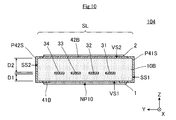
- FIG. 10 is a cross-sectional view taken along the line EE in FIG. 9 (A).
- 11 (A) is an external perspective view of the transmission line substrate 105 according to the fifth embodiment, and
- FIG. 11 (B) is a sectional view taken along line FF of FIG. 11 (A).
- FIG. 12 is an enlarged plan view showing the line portion SL of the transmission line board 106 according to the sixth embodiment.
- FIG. 13 is an exploded plan view of the line portion SL of the transmission line board 106.
- FIG. 1 is an external perspective view of the transmission line substrate 101 according to the first embodiment.
- FIG. 2 is an exploded plan view of the transmission line substrate 101.
- FIG. 3 is a cross-sectional view taken along the line AA in FIG. 4 (A) is a sectional view taken along line BB in FIG. 1, and
- FIG. 4 (B) is a sectional view taken along the line CC in FIG.
- the transmission line board 101 is, for example, an electronic component mounted on a single circuit board or a cable for connecting a plurality of circuit boards.
- the transmission line board 101 has connection portions CN1 and CN2 and a line portion SL.
- the connection portions CN1 and CN2 are portions connected to other circuit boards.
- the line section SL includes a transmission line (strip line) connecting the connecting sections CN1 and CN2.
- the connection portion CN1, the line portion SL, and the connection portion CN2 are arranged in this order in the + X direction.
- the transmission line substrate 101 includes a base material 10, input / output electrodes P1 and P2, a plurality of ground electrodes P31 and P32, a plurality of auxiliary electrodes P40, and a conductor pattern (signal line 31, first ground conductor 41, second ground conductor 42, A plurality of intermediate ground conductors 43), interlayer connecting conductors V1, V2, VG11, VG12, VG13, a first protective layer 1, a second protective layer 2, and the like are provided.
- the base material 10 is a substantially rectangular flat plate whose longitudinal direction coincides with the X-axis direction, and has a first main surface VS1 and a second main surface VS2 facing each other.
- the first main surface VS1 and the second main surface VS2 are planes parallel to the XY plane.
- the input / output electrodes P1 and the plurality of ground electrodes P31 are formed on the first main surface VS1 side of the connecting portion CN1, and the input / output electrodes P2 and the plurality of ground electrodes P32 are formed on the first main surface VS1 side of the connecting portion CN2. Is formed in.
- the plurality of auxiliary electrodes P40 are formed on the VS1 side of the first main surface of the line portion SL.
- the first ground conductor 41 and the first protective layer 1 are formed on the first main surface VS1.
- the second ground conductor 42 and the second protective layer 2 are formed on the second main surface VS2.
- the signal line 31, the plurality of intermediate ground conductors 43, the interlayer connecting conductors V1 and V2, and the plurality of interlayer connecting conductors VG11, VG12, and VG13 are formed inside the base material 10.
- the base material 10 is formed by laminating a plurality of base material layers 11, 12, and 13 in this order.
- the plurality of base material layers 11 to 13 are substantially rectangular resin (thermoplastic resin) flat plates whose longitudinal directions coincide with each other in the X-axis direction, and each has flexibility.
- the base material layers 11 to 13 are sheets mainly made of, for example, a liquid crystal polymer (LCP) or a polyetheretherketone (PEEK).
- Input / output electrodes P1 and P2 and a first ground conductor 41 are formed on the back surface of the base material layer 11.
- the input / output electrode P1 is a rectangular conductor pattern arranged near the first end (left end of the base material layer 11 in FIG. 2) in the longitudinal direction of the base material layer 11.
- the input / output electrode P2 is a rectangular conductor pattern arranged near the second end (right end of the base material layer 11 in FIG. 2) in the longitudinal direction of the base material layer 11.
- the first ground conductor 41 is a conductor pattern formed on substantially the entire surface of the base material layer 11.
- the first ground conductor 41 has three first conductor non-forming portions NP1.
- the first conductor non-forming portion NP1 is a rectangular opening (a portion without a conductor).
- the three first conductor non-forming portions NP1 are arranged in the X-axis direction.
- the input / output electrodes P1 and P2 and the first ground conductor 41 are conductor patterns such as Cu foil. Further, the interlayer connecting conductors V1 and V2 and a plurality of interlayer connecting conductors VG11 are formed on the base material layer 11.
- a signal line 31 and a plurality of intermediate ground conductors 43 are formed on the back surface of the base material layer 12.
- the signal line 31 is a linear conductor pattern extending in the transmission direction (X-axis direction).
- the plurality of intermediate ground conductors 43 are rectangular conductor patterns arranged near both ends in the longitudinal direction of the base material layer 12. Specifically, the three intermediate ground conductors 43 are arranged near the first end (left end of the base material layer 12 in FIG. 2) in the longitudinal direction of the base material layer 12. Further, the three intermediate ground conductors 43 are arranged near the second end (right end of the base material layer 12 in FIG. 2) in the longitudinal direction of the base material layer 12.
- the signal line 31 and the plurality of intermediate ground conductors 43 are conductor patterns such as Cu foil. Further, a plurality of interlayer connecting conductors VG12 are formed on the base material layer 12.
- a second ground conductor 42 is formed on the surface of the base material layer 13.
- the second ground conductor 42 is a conductor pattern formed on substantially the entire surface of the base material layer 13.
- the second ground conductor 42 has two second conductor non-forming portions NP2.
- the second conductor non-forming portion NP2 is a rectangular opening (a portion without a conductor).
- the two second conductor non-forming portions NP2 are arranged in the X-axis direction.
- the second ground conductor 42 is a conductor pattern such as Cu foil. Further, a plurality of interlayer connecting conductors VG13 are formed on the base material layer 13.
- the first protective layer 1 is a protective film formed on the back surface of the base material layer 11 (the first main surface of the base material 10).
- the plane shape of the first protective layer 1 is substantially the same as that of the base material layer 11.
- the first protective layer 1 is, for example, a coverlay film, a solder resist film, an epoxy resin film, or the like.
- the first protective layer 1 has rectangular openings AP1 and AP2, and a plurality of rectangular openings AP31, AP32, and AP40.
- the opening AP1 and the plurality of openings AP31 are arranged near the first end of the first protective layer 1 (the left end of the first protective layer 1 in FIG. 2).
- the opening AP2 and the plurality of openings AP32 are arranged near the second end of the first protective layer 1 (the right end of the first protective layer 1 in FIG. 2).
- the plurality of openings AP40 are arranged near the center in the longitudinal direction of the first protective layer 1 and are arranged in the X-axis direction.
- the opening AP1 is formed at a position corresponding to the position of the input / output electrode P1, and the opening AP2 is formed at a position corresponding to the position of the input / output electrode P2. Therefore, even when the first protective layer 1 is formed on the back surface of the base material layer 11, the input / output electrode P1 is exposed to the outside from the opening AP1, and the input / output electrode P2 is exposed to the outside from the opening AP2. Further, the plurality of openings AP31, AP32, AP40 are formed at positions corresponding to the positions of the first ground conductor 41.
- a part of the first ground conductor 41 is exposed to the outside from the plurality of openings AP31, AP32, AP40.
- a part of the first ground conductor 41 exposed from the opening AP31 is the ground electrode P31
- a part of the first ground conductor 41 exposed from the opening AP32 is the ground electrode P32
- the opening AP40 is an auxiliary electrode P40.
- the second protective layer 2 is a protective film formed on the surface of the base material layer 13 (second main surface VS2 of the base material 10).
- the plane shape of the second protective layer 2 is substantially the same as that of the base material layer 13.
- the second protective layer 2 is, for example, a coverlay film, a solder resist film, an epoxy resin film, or the like.
- the input / output electrodes P1 and P2 are electrically connected to the signal line 31. Specifically, as shown in FIG. 3 and the like, one end of the signal line 31 is connected to the input / output electrode P1 via the interlayer connection conductor V1, and the other end of the signal line 31 is connected via the interlayer connection conductor V2. It is connected to the input / output electrode P2. Further, the first ground conductor 41 and the second ground conductor 42 are electrically connected to each other via the intermediate ground conductor 43 and the interlayer connecting conductors VG11, VG12, and VG13, respectively.
- the signal line 31 in the line portion SL is arranged between the first ground conductor 41 and the second ground conductor 42 in the Z-axis direction. ..
- a transmission line (strip line) including a signal line 31, a first ground conductor 41, and a second ground conductor 42 is configured in the line portion SL of the transmission line substrate 101.
- the gap D1 between the signal line 31 and the first ground conductor 41 in the Z-axis direction is smaller than the gap D2 between the signal line 31 and the second ground conductor 42 in the Z-axis direction (D1 ⁇ D2).
- the plurality of first conductor non-forming portions NP1 are viewed in a plan view of the first main surface VS1 and the second main surface VS2 (viewed from the Z-axis direction). , Is arranged at a position overlapping the signal line 31.
- the plurality of second conductor non-forming portions NP2 are arranged at positions overlapping the signal line 31 when viewed from the Z-axis direction.
- the width of the first conductor non-forming portion NP1 (width in the Y-axis direction) and the width of the second conductor non-forming portion NP2 are larger than the line width of the signal line 31 (width in the Y-axis direction).
- the total area of the plurality of second conductor non-forming portions NP2 is larger than the total area of the plurality of first conductor non-forming portions NP1.
- the first protective layer 1 and the second protective layer 2 of the present embodiment are made of a material having a higher relative permittivity than the base material 10 (base material layers 11 to 13). Further, as shown in FIG. 4A, the first protective layer 1 is arranged at a position covering the first conductor non-forming portion NP1 when viewed from the Z-axis direction. Further, as shown in FIG. 4B, the second protective layer 2 is arranged at a position covering the second conductor non-forming portion NP2 when viewed from the Z-axis direction.
- FIG. 5 is a cross-sectional view showing a main part of the electronic device 301 according to the first embodiment.
- the electronic device 301 includes a transmission line board 101, circuit boards 201, 202, active elements 51, 52, and the like.
- the electronic device 301 also includes other elements, but is not shown in FIG.
- the circuit boards 201 and 202 are, for example, glass / epoxy boards.
- the active elements 51 and 52 are, for example, semiconductor elements, ICs, and the like.
- the circuit boards 201 and 202 are arranged to face each other. Specifically, the first surface PS1 of the circuit board 201 faces the second surface PS2 of the circuit board 202.
- the first surface PS1 of the circuit board 201 is provided with substrate side electrodes EP1, EP2, EP31, EP32, EP40 and a protective layer 3.
- a plurality of substrate-side electrodes EP5 and EP6 are provided on the second surface PS2 of the circuit board 202.
- the protective layer 3 has a higher relative permittivity than the base material 10 (or the base material of the circuit board 201).
- the protective layer 3 is, for example, a coverlay film, a solder resist film, an epoxy resin, or the like.
- the transmission line board 101 is surface-mounted on the circuit board 201 with the first main surface VS1 facing the first surface PS1 of the circuit board 201. Specifically, the input / output electrodes P1 and P2 of the transmission line board 101 are joined to the substrate side electrodes EP1 and EP2 of the circuit board 201 via a conductive bonding material such as solder. Further, the other electrodes (ground electrodes P31, P32 and auxiliary electrodes P40) of the transmission line substrate 101 are bonded to the substrate side electrodes EP31, EP32, and EP40 of the circuit board 201, respectively, via a conductive bonding material.
- Active elements 51 and 52 are mounted on the second surface PS2 of the circuit board 202. Specifically, the input / output terminals of the active element 51 are joined to the substrate side electrode EP5 of the circuit board 202, and the input / output terminals of the active element 52 are connected to the substrate side electrode EP6 of the circuit board 202. As shown in FIG. 5, the active elements 51 and 52 are arranged closer to the second main surface VS2 than the first main surface VS1 of the line portion SL.
- the total area of the second conductor non-forming portion NP2 of the second ground conductor 42 located on the top surface (second main surface VS2) side is set to the mounting surface (first main surface VS1) side. It is smaller than the total area of the first conductor non-forming portion NP1 of the first ground conductor 41 located. That is, in the transmission line substrate 101 according to the present embodiment, the first ground conductor 41 having a relatively low conductor ratio is arranged on the mounting surface side, and the second ground conductor 42 having a relatively high conductor ratio is arranged on the top surface side. Have been placed.
- this configuration as compared with the case where the first ground conductor having a relatively low conductor ratio is located on the top surface side, from the outside (particularly, the second main surface VS2 side) to the transmission line (signal line 31). The influence of noise can be suppressed. In addition, this configuration also suppresses unnecessary high-frequency radiation from the transmission line.
- a plurality of first conductor non-forming portions NP1 are formed at positions of the first ground conductor 41 that overlap the signal line 31 when viewed from the Z-axis direction. Further, in the present embodiment, a plurality of second conductor non-forming portions NP2 are formed at positions of the second ground conductor 42 that overlap the signal line 31 when viewed from the Z-axis direction.
- the first protective layer 1 having a relative permittivity higher than that of the base material 10 is formed on the first main surface VS1. According to this configuration, unnecessary radiation from the first conductor non-forming portion NP1 to the first main surface VS1 side (outside, circuit board 201 side) and unnecessary radiation from the first main surface VS1 side can be suppressed. In particular, by arranging the first protective layer 1 at a position covering the first conductor non-forming portion NP1 when viewed from the Z-axis direction as in the present embodiment, the effect of suppressing unnecessary radiation is enhanced.
- the circuit board 201 since the relative permittivity of the protective layer 3 formed on the first surface PS1 of the circuit board 201 is higher than that of the base material 10 (or the base material of the circuit board 201), the circuit board 201 Unnecessary radiation (or unnecessary radiation to the circuit board 201) is further suppressed.
- the active elements 51 and 52 that easily generate noise are located on the second main surface VS2 (top surface of the transmission line substrate 102).
- the area of the non-conductor forming portion of the second ground conductor 42 located on the second main surface VS2 side is relatively small, the area of the non-conductor forming portion of the ground conductor located on the second main surface VS2 side is relatively small. Compared to the case where it is large, it is less affected by noise from the active elements 51 and 52.
- the second protective layer 2 having a relative permittivity higher than that of the base material 10 is formed on the second main surface VS2. According to this configuration, unnecessary radiation from the second conductor non-forming portion NP2 to the second main surface VS2 side (outside) and unnecessary radiation from the second main surface VS2 side can be suppressed. In particular, by arranging the second protective layer 2 at a position covering the second conductor non-forming portion NP2 when viewed from the Z-axis direction as in the present embodiment, the effect of suppressing unnecessary radiation is further enhanced.
- the first conductor non-forming portion NP1 and the second conductor non-forming portion NP2 do not overlap when viewed from the Z-axis direction. With this configuration, it is possible to suppress a sudden change in the characteristic impedance in the line section SL (transmission line). That is, it is easy to ensure the continuity of the characteristic impedance in the line portion SL.
- the auxiliary electrode P40 is arranged between the connecting portions CN1 and CN2 when viewed from the Z-axis direction. According to this configuration, the self-alignment function of the conductive bonding material that joins the auxiliary electrode P40 and the substrate side electrode EP40 makes it possible to prevent the line portion SL from being displaced. Further, in the present embodiment, since the plurality of auxiliary electrodes P40 are provided along the transmission direction, even if the connection portion CN1 and CN2 (line portion SL) have a long shape, that is, the shape is easily deformed. However, the transmission line board 101 can be mounted on the circuit board 201 with high accuracy while keeping the shape of the transmission line board 101 (particularly the line portion SL) constant.
- connection portion of the present invention is a portion that connects an input / output electrode or the like of a transmission line board to another board (another circuit board, another transmission line board, etc.), and sends a signal to the other board.
- the part to be transmitted refers to an opening portion of the ground conductor (an opening portion in which the input / output electrodes connected to the signal line are arranged inside) when viewed from the Z-axis direction.
- the "line portion” of the present invention refers to a region other than those connecting portions when both ends of the transmission direction (direction along the signal line) are connected portions. It should be noted that the "connection portion” is preferably wider than the line portion because it is assumed that the "connection portion” is directly solder-mounted on an external circuit board or a connector is mounted.
- first ground conductor and the “second ground conductor” of the present invention are considered to overlap when viewed from the Z-axis direction (stacking direction or thickness direction). That is, the "first conductor non-forming portion” of the present invention refers to a portion that overlaps the second ground conductor and has no first ground conductor when viewed from the Z-axis direction. Further, the “second conductor non-forming portion” of the present invention refers to a portion that overlaps with the first ground conductor and a portion without the second ground conductor when viewed from the Z-axis direction.
- the active elements 51 and 52 show the electronic device 301 closer to the second main surface VS2 than the first main surface VS1 of the line portion SL, but the present invention is not limited to this configuration. ..
- the antenna or the conductor for another circuit is closer to the second main surface VS2 than the first main surface VS1 of the line portion SL, the same action / effect is obtained.
- the transmission line substrate 101 according to this embodiment is manufactured, for example, in the following process.
- the base material layers 11 to 13 are sheets mainly made of a thermoplastic resin such as a liquid crystal polymer (LCP) or a polyetheretherketone (PEEK).
- LCP liquid crystal polymer
- PEEK polyetheretherketone
- input / output electrodes P1 and P2 and conductor patterns (signal line 31, first ground conductor 41, second ground conductor 42, and a plurality of intermediate ground conductors 43) are applied to the plurality of base material layers 11 to 13.
- a metal foil for example, Cu foil
- the metal foil is patterned by photolithography.
- the input / output electrodes P1 and P2 and the first ground conductor 41 are formed on the back surface of the base material layer 11, and the signal line 31 and the plurality of intermediate ground conductors 43 are formed on the back surface of the base material layer 12.
- a second ground conductor 42 is formed on the surface of 13.
- first conductor non-forming portions NP1 are provided at predetermined positions of the first ground conductor 41.
- second conductor non-forming portions NP2 are provided at predetermined positions of the second ground conductor 42.
- the total area of the plurality of second conductor non-forming portions NP2 is smaller than the total area of the plurality of first conductor non-forming portions NP1.
- interlayer connecting conductors V1 and V2 and a plurality of interlayer connecting conductors VG11, VG12 and VG13 are formed on the base material layers 11 to 13, respectively.
- holes through holes
- a conductive paste containing a metal powder such as Cu, Sn or an alloy thereof and a resin material is arranged in the holes. It is provided by (filling) and solidifying the conductive paste by a subsequent heat press treatment.
- the plurality of base material layers 11, 12, and 13 are laminated (placed) in this order, and the laminated base material layers 11 to 13 are heat-pressed (collectively pressed) to form the base material 10.
- the signal line 31 is arranged between the first ground conductor 41 and the second ground conductor 42 in the Z-axis direction.
- the plurality of first conductor non-forming portions NP1 and the plurality of second conductor non-forming portions NP2 are arranged at positions overlapping the signal lines 31 when viewed from the Z-axis direction.
- the first protective layer 1 is formed on the first main surface VS1 (the back surface of the base material layer 11) of the base material 10, and is formed on the second main surface VS2 (the surface of the base material layer 13) of the base material 10.
- the second protective layer 2 is formed to obtain the transmission line substrate 101.
- the first protective layer 1 and the second protective layer 2 are, for example, a coverlay film, a solder resist film, an epoxy resin, or the like.
- a thin transmission line substrate that can suppress the influence of external noise can be easily manufactured even if the ground conductor is provided with a non-conductor forming portion.
- the base material 10 can be easily formed by laminating a plurality of base material layers 11 to 13 mainly made of a thermoplastic resin and heat-pressing (batch pressing). The number of processes can be reduced and the cost can be kept low.
- the conductive paste is arranged in the holes provided in the base material layer, and the conductive paste is solidified by a heating press (collective press), so that the step of forming the interlayer connection conductor can be reduced. ..
- Second Embodiment an example of a transmission line substrate in which the second ground conductor is not provided with a non-conductor forming portion is shown.
- FIG. 6 is an external perspective view of the transmission line board 102 according to the second embodiment.
- FIG. 7 is an exploded plan view of the transmission line substrate 102.
- the transmission line board 102 is different from the transmission line board 101 according to the first embodiment in that it includes a solid second ground conductor 42A in which a non-conductor-forming portion is not provided. Other configurations of the transmission line board 102 are the same as those of the transmission line board 101.
- the second ground conductor 42A has a solid conductor pattern. According to this configuration, the electromagnetic field of the line portion SL is higher than that of the transmission line substrate provided with the second ground conductor provided with the non-conductor forming portion (see the transmission line substrate 101 according to the first embodiment). The shielding effect is enhanced.
- Third Embodiment an example of a transmission line board including a plurality of signal lines is shown.
- FIG. 8A is an external perspective view of the transmission line substrate 103 according to the third embodiment
- FIG. 8B is a sectional view taken along line DD in FIG. 8A.
- the transmission line substrate 103 includes a base material 10A, input / output electrodes P11, P12, P13, P14, P21, P22, P23, P24, a plurality of signal lines 31, 32, 33, 34, a first ground conductor 41A, and a second ground. It differs from the transmission line substrate 101 according to the first embodiment in that it includes conductors 42A, four auxiliary electrodes P41, and a plurality of interlayer connection conductors VG21, VG22, and VG23. Other configurations of the transmission line board 103 are the same as those of the transmission line board 101.
- the base material 10A has a wider width in the width direction (Y-axis direction) than the base material 10 described in the first embodiment.
- Other configurations of the base material 10A are the same as those of the base material 10.
- the input / output electrodes P11 to P14 and the three ground electrodes P31 are formed on the first main surface VS1 side of the connecting portion CN1.
- the input / output electrodes P21 to P24 and the three ground electrodes P32 are formed on the first main surface VS1 side of the connecting portion CN2.
- the four auxiliary electrodes P41 are formed on the VS1 side of the first main surface of the line portion SL.
- the signal lines 31 to 34, the first ground conductor 41A, the second ground conductor 42A, the intermediate ground conductor 43, and the interlayer connecting conductors VG21, VG22, and VG23 are formed inside the line portion SL (base material 10A).
- Each of the plurality of signal lines 31 to 34 is a linear conductor pattern extending in the transmission direction (X-axis direction).
- the plurality of signal lines 31 to 34 have portions that run in parallel with each other in the line portion SL. Further, the signal lines 31, 32, 33, and 34 are arranged in this order in the + Y direction. Further, in the present embodiment, the signal lines 31 to 34 are arranged in the same layer in the Z-axis direction (stacking direction or thickness direction).
- the first ground conductor 41A is different from the first ground conductor 41 described in the first embodiment in that the first conductor non-forming portions NP11 and NP12 are provided.
- the first conductor non-forming portions NP11 and NP12 are elongated openings (recessed portions) extending in the X-axis direction, and are formed on the outer periphery of the first ground conductor 41A.
- the first conductor non-forming portions NP11 and NP12 are arranged in this order in the + Y direction.
- the first ground conductor 41A is a linear conductor pattern extending in the transmission direction.
- the second ground conductor 42A is different from the second ground conductor 42 described in the first embodiment in that a non-conductor forming portion is not formed.
- Other configurations of the second ground conductor 42A are the same as those of the second ground conductor 42.
- the four auxiliary electrodes P41 are arranged near the center in the width direction (Y-axis direction) of the line portion SL, and are arranged in the transmission direction (X-axis direction). Further, the plurality of interlayer connection conductors VG21 to VG23 are respectively arranged near the center in the width direction of the line portion SL. Although not shown, the plurality of interlayer connection conductors VG21 to VG23 are arranged in the transmission direction (X-axis direction).
- the input / output electrodes P11 and P21 are electrically connected to the signal line 31, the input / output electrodes P12 and P22 are electrically connected to the signal line 32, and the input / output electrodes P13 and P23 are connected to the signal line 33. It is electrically connected, and the input / output electrodes P14 and P24 are electrically connected to the signal line 34. Further, the first ground conductor 41A and the second ground conductor 42A are electrically connected to each other in the line portion SL via the intermediate ground conductor 43 and the interlayer connecting conductors VG21, VG22, and VG23.
- the signal lines 31 to 34 in the line portion SL are arranged between the first ground conductor 41A and the second ground conductor 42A in the Z-axis direction.
- the line portion SL of the transmission line substrate 102 includes a transmission line (microstrip line) including signal lines 31 to 34 and a second ground conductor 42A.
- the gap D1 between the signal lines 31 to 34 and the first ground conductor 41A in the Z-axis direction is smaller than the gap D2 between the signal lines 31 to 34 and the second ground conductor 42A in the Z-axis direction (D1 ⁇ D2). ..
- grounds intermediate ground conductor 43 and interlayer connection conductors VG21 to VG23
- the signal lines 31 and 32 and the signal lines 33 and 34 are arranged between the signal lines 31 and 32 and the signal lines 33 and 34. ing. With this configuration, isolation between the signal lines 31 and 32 and the signal lines 33 and 34 is ensured, and crosstalk is suppressed.
- the four auxiliary electrodes P41 are arranged at equal intervals in the transmission direction. According to this configuration, even if the line portion SL (between the connection portions CN1 and CN2) is long, abnormal movement of the line portion SL with respect to the circuit board can be suppressed at the time of joining by the reflow soldering method or the like.
- the present embodiment shows an example in which a plurality of signal lines 31 to 34 are arranged in the same layer in the Z-axis direction, the present embodiment is not limited to this configuration.
- the plurality of signal lines may be arranged in different layers in the Z-axis direction.
- FIG. 9 (A) is an external perspective view of the transmission line board 104 according to the fourth embodiment
- FIG. 9 (B) is a plan view of the transmission line board 104
- FIG. 10 is a cross-sectional view taken along the line EE in FIG. 9 (A).
- the transmission line substrate 104 includes a base material 10B, input / output electrodes P11, P12, P13, P14, P21, P22, P23, P24, a plurality of signal lines 31, 32, 33, 34, a first ground conductor 41B, and a second ground. It differs from the transmission line substrate 104 according to the first embodiment in that it includes a conductor 42B, a plurality of auxiliary electrodes P41S, P42S, and the like.
- the base material 10B is a rectangular flat plate whose longitudinal direction coincides with the X-axis direction.
- the base material 10B has a first main surface VS1, a second main surface VS2, and side surfaces SS1 and SS2.
- the side surfaces SS1 and SS2 are planes parallel to the XZ plane, adjacent to the first main surface VS1 and the second main surface VS2.
- Other configurations of the base material 10B are the same as those of the base material 10 described in the first embodiment.
- the input / output electrodes P11 to P14 are formed on the first main surface VS1 side of the connecting portion CN1.
- the input / output electrodes P21 to P24 are formed on the first main surface VS1 side of the connecting portion CN2.
- the signal lines 31 to 34 are formed inside the base material 10B.
- the auxiliary electrode P41S is formed so as to straddle the first main surface VS1, the side surface SS1, and the second main surface VS2.
- the auxiliary electrode P42S is formed so as to straddle the first main surface VS1, the side surface SS2, and the second main surface VS2.
- the three auxiliary electrodes P41S and the three auxiliary electrodes P42S are arranged in the + X direction, respectively.
- the auxiliary electrodes P41S and P42S are plating films such as Cu formed on the side surfaces SS1 and SS2 by, for example, electric field plating. Further, the auxiliary electrodes P41S and P42S may be a metal film such as Cu formed by a sputtering method.
- Each of the plurality of signal lines 31 to 34 is a linear conductor pattern extending in the transmission direction (X-axis direction).
- the plurality of signal lines 31 to 34 have portions that run in parallel with each other in the line portion SL. Further, the signal lines 31, 32, 33, and 34 are arranged in this order in the + Y direction. Further, in the present embodiment, the signal lines 31 to 34 are arranged in the same layer in the Z-axis direction.
- the first ground conductor 41B is different from the first ground conductor 41 described in the first embodiment in that the first conductor non-forming portion NP10 is provided.
- the first ground conductor 41B is a rectangular conductor pattern.
- the first conductor non-forming portion NP10 is an opening arranged near the center of the first ground conductor 41A.
- the second ground conductor 42B is different from the second ground conductor 42 described in the first embodiment in that a non-conductor forming portion is not formed.
- the second ground conductor 42B is a rectangular conductor pattern. Other configurations of the second ground conductor 42B are the same as those of the second ground conductor 42.
- the input / output electrodes P11 and P21 are electrically connected to the signal line 31, the input / output electrodes P12 and P22 are electrically connected to the signal line 32, and the input / output electrodes P13 and P23 are connected to the signal line 33. It is electrically connected, and the input / output electrodes P14 and P24 are electrically connected to the signal line 34. Further, the first ground conductor 41B and the second ground conductor 42B are electrically connected to each other via auxiliary electrodes P41S, P42S and the like.
- the signal lines 31 to 34 are arranged between the first ground conductor 41B and the second ground conductor 42B in the Z-axis direction.
- the line portion SL of the transmission line substrate 104 includes a transmission line (microstrip line) including signal lines 31 to 34 and a second ground conductor 42A.
- the gap D1 between the signal lines 31 to 34 and the first ground conductor 41B in the Z-axis direction is smaller than the gap D2 between the signal lines 31 to 34 and the second ground conductor 42B in the Z-axis direction (D1 ⁇ D2). ..
- FIG. 11 (A) is an external perspective view of the transmission line substrate 105 according to the fifth embodiment
- FIG. 11 (B) is a sectional view taken along line FF of FIG. 11 (A).
- the transmission line board 105 is different from the transmission line board 103 according to the third embodiment in that it includes a first ground conductor 41C, a second ground conductor 42A, four auxiliary electrodes P41, P42, P43, and the like. Other configurations of the transmission line board 105 are the same as those of the transmission line board 103.
- the first ground conductor 41C is different from the first ground conductor 41A described in the third embodiment in that the first conductor non-forming portions NP11A and NP12A are provided.
- the first conductor non-forming portions NP11A and NP12A are elongated openings extending in the X-axis direction.
- the first conductor non-forming portions NP11A and NP12A are arranged in this order in the + Y direction.
- the auxiliary electrodes P41, P42, and P43 are arranged in this order in the + Y direction. Specifically, the auxiliary electrode P41 is arranged near the center of the line portion SL in the width direction (Y-axis direction), the auxiliary electrode P42 is arranged near the side surface SS1 of the line portion SL, and the auxiliary electrode P43 is arranged near the line portion SL. It is arranged near the side surface SS2 of.
- the auxiliary electrode P41 is the same as that described in the third embodiment.
- the four auxiliary electrodes P41, P42, and P43, respectively, are arranged in the transmission direction (X-axis direction).
- the first ground conductor 41C and the second ground conductor 42A are electrically connected to each other via the intermediate ground conductor 43 and the interlayer connecting conductors VG21 to VG23.
- the signal lines 31 and 32 have grounds (second ground conductor 42A, intermediate ground conductor 43, and interlayer connection conductors VG21 to VG23) arranged in three directions around the signal lines 31 and 32. .. That is, the signal lines 31 and 32 are surrounded by grounds in three directions. Further, the signal lines 33 and 34 are surrounded in three directions by grounds (second ground conductor 42A, intermediate ground conductor 43, and interlayer connection conductors VG21 to VG23). That is, the signal lines 33 and 34 are surrounded by grounds in three directions. According to this configuration, sufficient isolation between the signal lines 31 and 32 and the signal lines 33 and 34 is sufficiently secured, and the effect of suppressing crosstalk is further enhanced.
- auxiliary electrode has a planar shape extending in an oblique direction with respect to the transmission direction.
- FIG. 12 is an enlarged plan view showing the line portion SL of the transmission line board 106 according to the sixth embodiment.
- FIG. 13 is an exploded plan view of the line portion SL of the transmission line board 106.
- signal lines 31, 32, 33, 34, 35, and 36 are shown by dot patterns in order to make the structure easy to understand.
- the transmission line substrate 106 includes a plurality of auxiliary electrodes P46, six signal lines 31, 32, 33, 34, 35, 36, a first ground conductor 41D, an intermediate ground conductor 43D, and the like. It is different from the transmission line board 103. Other configurations of the transmission line board 103 are the same as those of the transmission line board 103.
- the plurality of auxiliary electrodes P46 are formed on the VS1 side of the first main surface of the line portion SL. As shown in FIG. 12 and the like, the plurality of auxiliary electrodes P46 have a planar shape extending in an oblique direction with respect to the transmission direction (X-axis direction).
- Each of the six signal lines 31 to 36 is a linear conductor pattern extending in the transmission direction (approximately the X-axis direction).
- the six signal lines 31 to 36 have portions that run in parallel with each other in the line portion SL.
- the signal lines 31, 32, 33, 34, 35, 36 are arranged in this order in the + Y direction.
- the intermediate ground conductor 43D is arranged in the same layer as the signal lines 31 to 36 in the Z-axis direction. Further, the intermediate ground conductor 43D is arranged between two adjacent signal lines among the plurality of signal lines 31 to 36, and runs parallel to the plurality of signal lines 31 to 36 in the line portion SL.
- the first ground conductor 41D is different from the first ground conductor 41A described in the third embodiment in that it has a mesh shape in which a plurality of first conductor non-forming portions NP10D are provided.
- the first conductor non-forming portion NP10D is a long opening having a longitudinal direction substantially in the X-axis direction.
- a plurality of first conductor non-forming portions NP10D having substantially the same shape are periodically arranged. More specifically, the plurality of first conductor non-forming portions NP10D are staggered when viewed from the Z-axis direction.
- the plurality of auxiliary electrodes P46 have a planar shape extending diagonally with respect to the transmission direction (X-axis direction). According to this configuration, the fluctuation width of the GND potential in the transmission direction can be reduced as compared with the case where the auxiliary electrode has a planar shape extending in the width direction (Y-axis direction).
- a plurality of first conductor non-forming portions NP10D having substantially the same shape are periodically arranged. According to this configuration, the fluctuation range of the GND potential in the transmission direction can be reduced, and the continuity of the characteristic impedance in the line portion SL can be easily ensured. This also applies to a plurality of second conductor non-forming portions provided on the second ground conductor.
- the first conductor non-forming portions NP10D overlapping the different signal lines are arranged (overlapping) adjacent to each other in the width direction, but the configuration is not limited to this. Absent. When viewed from the Z-axis direction, it is preferable that the plurality of first conductor non-forming portions (overlapping on different signal lines) are not arranged adjacent to each other in the width direction (do not overlap). According to this configuration, crosstalk between a plurality of signal lines can be suppressed. This also applies to a plurality of second conductor non-forming portions provided on the second ground conductor.
- connection portion In each of the above embodiments, an example in which the input / output electrode and the ground electrode provided in the connection portion are bonded to the substrate side electrode of the circuit board via the conductive bonding material is shown, but the configuration is limited to this. It is not something that is done.
- a connector may be provided at the connection portion of the transmission line board, or the connection portion may be connected to the receptacle of the circuit board.
- connection portions CN1 and CN2 and one line portion SL have been shown, but the present invention is not limited to this configuration.
- the number of connection portions and the number of line portions of the transmission line substrate can be appropriately changed within the range in which the operation and effect of the present invention are exhibited, and the number of connection portions and the number of line portions may be one.
- the structure may be such that the antenna, the line portion SL, and the connection portion are arranged in this order in the + X direction.
- the base material included in the transmission line substrate is a rectangular or substantially rectangular flat plate, but the present invention is not limited to this configuration.
- the shape of the laminate can be appropriately changed within the range in which the action and effect of the present invention are exhibited.
- the planar shape of the laminated body may be, for example, polygonal, circular, elliptical, L-shaped, T-shaped, Y-shaped, U-shaped, crank-shaped, or the like.
- a transmission line substrate including a substrate formed by laminating three substrate layers has been shown, but the present invention is not limited to this configuration.
- the number of laminated base material layers contained in the base material can be appropriately changed within the range in which the actions and effects of the present invention are exhibited.
- the first protective layer 1 and the second protective layer 2 are not essential in the transmission line substrate.
- the base material has a plurality of base material layers made of a thermoplastic resin, but the structure is not limited to this.
- the plurality of base material layers may be a sheet made of a thermosetting resin.
- the plurality of base material layers may be a dielectric ceramic sheet of low temperature co-fired ceramics (LTCC).
- the base material may be a composite laminate of a plurality of resins, or may be formed by laminating a thermosetting resin sheet such as a glass / epoxy substrate and a thermoplastic resin sheet.
- the base material is not limited to one in which a plurality of base material layers are heat-pressed (collectively pressed) to fuse the surfaces thereof, and an adhesive layer may be provided between each base material layer.
- the gap D1 between the signal line and the first ground conductor in the Z-axis direction is smaller than the gap D2 between the signal line and the second ground conductor in the Z-axis direction.
- the gap D1 may be larger than the gap D2, and the gaps D1 and D2 may be equal.
- the transmission direction (where the signal line extends) coincides with the X-axis direction
- the transmission direction may be, for example, the Y-axis direction, or may be bent in the X-axis direction and the Y-axis direction.
- the circuit formed on the transmission line substrate is not limited to the configuration of each of the above-described embodiments, and can be appropriately changed as long as the operation / effect of the present invention is exhibited.
- the circuit formed on the transmission line substrate is, for example, a coil composed of a conductor pattern, a capacitor composed of a conductor pattern, and a frequency filter such as various filters (low-pass filter, high-pass filter, band-pass filter, band-elimination filter). May be configured.
- various other transmission lines may be formed on the transmission line substrate.
- various electronic components such as chip components may be mounted or embedded in the transmission line board.
- transmission line board in which one, four, or six signal lines are arranged in a line portion is shown, but the present invention is not limited to this configuration.
- the number of signal lines (transmission lines) can be appropriately changed depending on the circuit configuration of the transmission line board.
- the plurality of signal lines may be used in the same system (same frequency band), or may be used in different systems (different frequency bands).
Landscapes
- Engineering & Computer Science (AREA)
- Microelectronics & Electronic Packaging (AREA)
- Manufacturing & Machinery (AREA)
- Physics & Mathematics (AREA)
- Electromagnetism (AREA)
- Structure Of Printed Boards (AREA)
- Combinations Of Printed Boards (AREA)
- Waveguides (AREA)
Priority Applications (3)
| Application Number | Priority Date | Filing Date | Title |
|---|---|---|---|
| JP2021536858A JP7143954B2 (ja) | 2019-07-31 | 2020-07-02 | 伝送線路基板および電子機器 |
| CN202090000572.9U CN217062060U (zh) | 2019-07-31 | 2020-07-02 | 传输线路基板以及电子设备 |
| US17/514,215 US12046792B2 (en) | 2019-07-31 | 2021-10-29 | Transmission line substrate and electronic device |
Applications Claiming Priority (2)
| Application Number | Priority Date | Filing Date | Title |
|---|---|---|---|
| JP2019-141239 | 2019-07-31 | ||
| JP2019141239 | 2019-07-31 |
Related Child Applications (1)
| Application Number | Title | Priority Date | Filing Date |
|---|---|---|---|
| US17/514,215 Continuation US12046792B2 (en) | 2019-07-31 | 2021-10-29 | Transmission line substrate and electronic device |
Publications (1)
| Publication Number | Publication Date |
|---|---|
| WO2021020019A1 true WO2021020019A1 (ja) | 2021-02-04 |
Family
ID=74230587
Family Applications (1)
| Application Number | Title | Priority Date | Filing Date |
|---|---|---|---|
| PCT/JP2020/025996 Ceased WO2021020019A1 (ja) | 2019-07-31 | 2020-07-02 | 伝送線路基板および電子機器 |
Country Status (4)
| Country | Link |
|---|---|
| US (1) | US12046792B2 (https=) |
| JP (1) | JP7143954B2 (https=) |
| CN (1) | CN217062060U (https=) |
| WO (1) | WO2021020019A1 (https=) |
Citations (3)
| Publication number | Priority date | Publication date | Assignee | Title |
|---|---|---|---|---|
| JP3173143U (ja) * | 2010-12-03 | 2012-01-26 | 株式会社村田製作所 | 高周波信号線路 |
| WO2016088592A1 (ja) * | 2014-12-01 | 2016-06-09 | 株式会社村田製作所 | 電子機器、電気素子および電気素子用トレイ |
| WO2019098012A1 (ja) * | 2017-11-16 | 2019-05-23 | 株式会社村田製作所 | 樹脂多層基板、電子部品およびその実装構造 |
Family Cites Families (2)
| Publication number | Priority date | Publication date | Assignee | Title |
|---|---|---|---|---|
| JP5041108B2 (ja) | 2010-12-03 | 2012-10-03 | 株式会社村田製作所 | 高周波信号線路 |
| WO2019188785A1 (ja) * | 2018-03-29 | 2019-10-03 | 株式会社村田製作所 | 伝送線路及びその実装構造 |
-
2020
- 2020-07-02 JP JP2021536858A patent/JP7143954B2/ja active Active
- 2020-07-02 WO PCT/JP2020/025996 patent/WO2021020019A1/ja not_active Ceased
- 2020-07-02 CN CN202090000572.9U patent/CN217062060U/zh active Active
-
2021
- 2021-10-29 US US17/514,215 patent/US12046792B2/en active Active
Patent Citations (3)
| Publication number | Priority date | Publication date | Assignee | Title |
|---|---|---|---|---|
| JP3173143U (ja) * | 2010-12-03 | 2012-01-26 | 株式会社村田製作所 | 高周波信号線路 |
| WO2016088592A1 (ja) * | 2014-12-01 | 2016-06-09 | 株式会社村田製作所 | 電子機器、電気素子および電気素子用トレイ |
| WO2019098012A1 (ja) * | 2017-11-16 | 2019-05-23 | 株式会社村田製作所 | 樹脂多層基板、電子部品およびその実装構造 |
Also Published As
| Publication number | Publication date |
|---|---|
| JPWO2021020019A1 (https=) | 2021-02-04 |
| US20220077555A1 (en) | 2022-03-10 |
| JP7143954B2 (ja) | 2022-09-29 |
| CN217062060U (zh) | 2022-07-26 |
| US12046792B2 (en) | 2024-07-23 |
Similar Documents
| Publication | Publication Date | Title |
|---|---|---|
| JP6156610B2 (ja) | 電子機器、およびアンテナ素子 | |
| JP7001158B2 (ja) | 多層基板、電子機器および多層基板の製造方法 | |
| CN211606926U (zh) | 内插器以及电子设备 | |
| JP5472555B2 (ja) | 高周波信号伝送線路及び電子機器 | |
| US10756462B2 (en) | Resin multilayer substrate and an electronic device and a joint structure of a resin multilayer substrate | |
| US11949144B2 (en) | Structure for mounting a transmission line substrate having interlayer connection conductors to another substrate by a conductive bonding material | |
| WO2018139382A1 (ja) | 多層基板および電子機器 | |
| US11145586B2 (en) | Interposer and electronic device | |
| JP7143954B2 (ja) | 伝送線路基板および電子機器 | |
| JP7167988B2 (ja) | 伝送線路基板、および伝送線路基板の接合構造 | |
| WO2020218267A1 (ja) | 伝送線路基板および電子機器 | |
| JP7095739B2 (ja) | 電気素子の製造方法 | |
| JP7287462B2 (ja) | 樹脂多層基板 | |
| CN218941409U (zh) | 电子设备 |
Legal Events
| Date | Code | Title | Description |
|---|---|---|---|
| 121 | Ep: the epo has been informed by wipo that ep was designated in this application |
Ref document number: 20847252 Country of ref document: EP Kind code of ref document: A1 |
|
| ENP | Entry into the national phase |
Ref document number: 2021536858 Country of ref document: JP Kind code of ref document: A |
|
| NENP | Non-entry into the national phase |
Ref country code: DE |
|
| 122 | Ep: pct application non-entry in european phase |
Ref document number: 20847252 Country of ref document: EP Kind code of ref document: A1 |