WO2021019707A1 - 3次元積層造形による回路配線の製造方法 - Google Patents
3次元積層造形による回路配線の製造方法 Download PDFInfo
- Publication number
- WO2021019707A1 WO2021019707A1 PCT/JP2019/029943 JP2019029943W WO2021019707A1 WO 2021019707 A1 WO2021019707 A1 WO 2021019707A1 JP 2019029943 W JP2019029943 W JP 2019029943W WO 2021019707 A1 WO2021019707 A1 WO 2021019707A1
- Authority
- WO
- WIPO (PCT)
- Prior art keywords
- circuit wiring
- heating
- glass transition
- transition point
- upper limit
- Prior art date
- Legal status (The legal status is an assumption and is not a legal conclusion. Google has not performed a legal analysis and makes no representation as to the accuracy of the status listed.)
- Ceased
Links
Images


Classifications
-
- B—PERFORMING OPERATIONS; TRANSPORTING
- B29—WORKING OF PLASTICS; WORKING OF SUBSTANCES IN A PLASTIC STATE IN GENERAL
- B29C—SHAPING OR JOINING OF PLASTICS; SHAPING OF MATERIAL IN A PLASTIC STATE, NOT OTHERWISE PROVIDED FOR; AFTER-TREATMENT OF THE SHAPED PRODUCTS, e.g. REPAIRING
- B29C64/00—Additive manufacturing, i.e. manufacturing of three-dimensional [3D] objects by additive deposition, additive agglomeration or additive layering, e.g. by 3D printing, stereolithography or selective laser sintering
- B29C64/10—Processes of additive manufacturing
- B29C64/106—Processes of additive manufacturing using only liquids or viscous materials, e.g. depositing a continuous bead of viscous material
-
- H—ELECTRICITY
- H05—ELECTRIC TECHNIQUES NOT OTHERWISE PROVIDED FOR
- H05K—PRINTED CIRCUITS; CASINGS OR CONSTRUCTIONAL DETAILS OF ELECTRIC APPARATUS; MANUFACTURE OF ASSEMBLAGES OF ELECTRICAL COMPONENTS
- H05K3/00—Apparatus or processes for manufacturing printed circuits
- H05K3/10—Apparatus or processes for manufacturing printed circuits in which conductive material is applied to the insulating support in such a manner as to form the desired conductive pattern
- H05K3/12—Apparatus or processes for manufacturing printed circuits in which conductive material is applied to the insulating support in such a manner as to form the desired conductive pattern using thick film techniques, e.g. printing techniques to apply the conductive material or similar techniques for applying conductive paste or ink patterns
- H05K3/1275—Apparatus or processes for manufacturing printed circuits in which conductive material is applied to the insulating support in such a manner as to form the desired conductive pattern using thick film techniques, e.g. printing techniques to apply the conductive material or similar techniques for applying conductive paste or ink patterns by other printing techniques, e.g. letterpress printing, intaglio printing, lithographic printing, offset printing
-
- B—PERFORMING OPERATIONS; TRANSPORTING
- B22—CASTING; POWDER METALLURGY
- B22F—WORKING METALLIC POWDER; MANUFACTURE OF ARTICLES FROM METALLIC POWDER; MAKING METALLIC POWDER; APPARATUS OR DEVICES SPECIALLY ADAPTED FOR METALLIC POWDER
- B22F1/00—Metallic powder; Treatment of metallic powder, e.g. to facilitate working or to improve properties
- B22F1/10—Metallic powder containing lubricating or binding agents; Metallic powder containing organic material
- B22F1/107—Metallic powder containing lubricating or binding agents; Metallic powder containing organic material containing organic material comprising solvents, e.g. for slip casting
-
- B—PERFORMING OPERATIONS; TRANSPORTING
- B33—ADDITIVE MANUFACTURING TECHNOLOGY
- B33Y—ADDITIVE MANUFACTURING, i.e. MANUFACTURING OF THREE-DIMENSIONAL [3D] OBJECTS BY ADDITIVE DEPOSITION, ADDITIVE AGGLOMERATION OR ADDITIVE LAYERING, e.g. BY 3D PRINTING, STEREOLITHOGRAPHY OR SELECTIVE LASER SINTERING
- B33Y70/00—Materials specially adapted for additive manufacturing
- B33Y70/10—Composites of different types of material, e.g. mixtures of ceramics and polymers or mixtures of metals and biomaterials
-
- H—ELECTRICITY
- H05—ELECTRIC TECHNIQUES NOT OTHERWISE PROVIDED FOR
- H05K—PRINTED CIRCUITS; CASINGS OR CONSTRUCTIONAL DETAILS OF ELECTRIC APPARATUS; MANUFACTURE OF ASSEMBLAGES OF ELECTRICAL COMPONENTS
- H05K1/00—Printed circuits
- H05K1/02—Details
- H05K1/03—Use of materials for the substrate
-
- H—ELECTRICITY
- H05—ELECTRIC TECHNIQUES NOT OTHERWISE PROVIDED FOR
- H05K—PRINTED CIRCUITS; CASINGS OR CONSTRUCTIONAL DETAILS OF ELECTRIC APPARATUS; MANUFACTURE OF ASSEMBLAGES OF ELECTRICAL COMPONENTS
- H05K3/00—Apparatus or processes for manufacturing printed circuits
- H05K3/10—Apparatus or processes for manufacturing printed circuits in which conductive material is applied to the insulating support in such a manner as to form the desired conductive pattern
- H05K3/12—Apparatus or processes for manufacturing printed circuits in which conductive material is applied to the insulating support in such a manner as to form the desired conductive pattern using thick film techniques, e.g. printing techniques to apply the conductive material or similar techniques for applying conductive paste or ink patterns
- H05K3/1241—Apparatus or processes for manufacturing printed circuits in which conductive material is applied to the insulating support in such a manner as to form the desired conductive pattern using thick film techniques, e.g. printing techniques to apply the conductive material or similar techniques for applying conductive paste or ink patterns by ink-jet printing or drawing by dispensing
- H05K3/125—Apparatus or processes for manufacturing printed circuits in which conductive material is applied to the insulating support in such a manner as to form the desired conductive pattern using thick film techniques, e.g. printing techniques to apply the conductive material or similar techniques for applying conductive paste or ink patterns by ink-jet printing or drawing by dispensing by ink-jet printing
-
- H—ELECTRICITY
- H05—ELECTRIC TECHNIQUES NOT OTHERWISE PROVIDED FOR
- H05K—PRINTED CIRCUITS; CASINGS OR CONSTRUCTIONAL DETAILS OF ELECTRIC APPARATUS; MANUFACTURE OF ASSEMBLAGES OF ELECTRICAL COMPONENTS
- H05K3/00—Apparatus or processes for manufacturing printed circuits
- H05K3/46—Manufacturing multilayer circuits
- H05K3/4644—Manufacturing multilayer circuits by building the multilayer layer by layer, i.e. build-up multilayer circuits
-
- B—PERFORMING OPERATIONS; TRANSPORTING
- B22—CASTING; POWDER METALLURGY
- B22F—WORKING METALLIC POWDER; MANUFACTURE OF ARTICLES FROM METALLIC POWDER; MAKING METALLIC POWDER; APPARATUS OR DEVICES SPECIALLY ADAPTED FOR METALLIC POWDER
- B22F10/00—Additive manufacturing of workpieces or articles from metallic powder
- B22F10/20—Direct sintering or melting
- B22F10/25—Direct deposition of metal particles, e.g. direct metal deposition [DMD] or laser engineered net shaping [LENS]
-
- B—PERFORMING OPERATIONS; TRANSPORTING
- B29—WORKING OF PLASTICS; WORKING OF SUBSTANCES IN A PLASTIC STATE IN GENERAL
- B29L—INDEXING SCHEME ASSOCIATED WITH SUBCLASS B29C, RELATING TO PARTICULAR ARTICLES
- B29L2031/00—Other particular articles
- B29L2031/34—Electrical apparatus, e.g. sparking plugs or parts thereof
- B29L2031/3425—Printed circuits
-
- B—PERFORMING OPERATIONS; TRANSPORTING
- B33—ADDITIVE MANUFACTURING TECHNOLOGY
- B33Y—ADDITIVE MANUFACTURING, i.e. MANUFACTURING OF THREE-DIMENSIONAL [3D] OBJECTS BY ADDITIVE DEPOSITION, ADDITIVE AGGLOMERATION OR ADDITIVE LAYERING, e.g. BY 3D PRINTING, STEREOLITHOGRAPHY OR SELECTIVE LASER SINTERING
- B33Y10/00—Processes of additive manufacturing
-
- B—PERFORMING OPERATIONS; TRANSPORTING
- B33—ADDITIVE MANUFACTURING TECHNOLOGY
- B33Y—ADDITIVE MANUFACTURING, i.e. MANUFACTURING OF THREE-DIMENSIONAL [3D] OBJECTS BY ADDITIVE DEPOSITION, ADDITIVE AGGLOMERATION OR ADDITIVE LAYERING, e.g. BY 3D PRINTING, STEREOLITHOGRAPHY OR SELECTIVE LASER SINTERING
- B33Y80/00—Products made by additive manufacturing
-
- H—ELECTRICITY
- H05—ELECTRIC TECHNIQUES NOT OTHERWISE PROVIDED FOR
- H05K—PRINTED CIRCUITS; CASINGS OR CONSTRUCTIONAL DETAILS OF ELECTRIC APPARATUS; MANUFACTURE OF ASSEMBLAGES OF ELECTRICAL COMPONENTS
- H05K2201/00—Indexing scheme relating to printed circuits covered by H05K1/00
- H05K2201/06—Thermal details
- H05K2201/068—Thermal details wherein the coefficient of thermal expansion is important
-
- H—ELECTRICITY
- H05—ELECTRIC TECHNIQUES NOT OTHERWISE PROVIDED FOR
- H05K—PRINTED CIRCUITS; CASINGS OR CONSTRUCTIONAL DETAILS OF ELECTRIC APPARATUS; MANUFACTURE OF ASSEMBLAGES OF ELECTRICAL COMPONENTS
- H05K2203/00—Indexing scheme relating to apparatus or processes for manufacturing printed circuits covered by H05K3/00
- H05K2203/01—Tools for processing; Objects used during processing
- H05K2203/0104—Tools for processing; Objects used during processing for patterning or coating
- H05K2203/013—Inkjet printing, e.g. for printing insulating material or resist
-
- H—ELECTRICITY
- H05—ELECTRIC TECHNIQUES NOT OTHERWISE PROVIDED FOR
- H05K—PRINTED CIRCUITS; CASINGS OR CONSTRUCTIONAL DETAILS OF ELECTRIC APPARATUS; MANUFACTURE OF ASSEMBLAGES OF ELECTRICAL COMPONENTS
- H05K2203/00—Indexing scheme relating to apparatus or processes for manufacturing printed circuits covered by H05K3/00
- H05K2203/11—Treatments characterised by their effect, e.g. heating, cooling, roughening
- H05K2203/1131—Sintering, i.e. fusing of metal particles to achieve or improve electrical conductivity
-
- H—ELECTRICITY
- H05—ELECTRIC TECHNIQUES NOT OTHERWISE PROVIDED FOR
- H05K—PRINTED CIRCUITS; CASINGS OR CONSTRUCTIONAL DETAILS OF ELECTRIC APPARATUS; MANUFACTURE OF ASSEMBLAGES OF ELECTRICAL COMPONENTS
- H05K3/00—Apparatus or processes for manufacturing printed circuits
- H05K3/10—Apparatus or processes for manufacturing printed circuits in which conductive material is applied to the insulating support in such a manner as to form the desired conductive pattern
- H05K3/12—Apparatus or processes for manufacturing printed circuits in which conductive material is applied to the insulating support in such a manner as to form the desired conductive pattern using thick film techniques, e.g. printing techniques to apply the conductive material or similar techniques for applying conductive paste or ink patterns
- H05K3/1283—After-treatment of the printed patterns, e.g. sintering or curing methods
-
- H—ELECTRICITY
- H05—ELECTRIC TECHNIQUES NOT OTHERWISE PROVIDED FOR
- H05K—PRINTED CIRCUITS; CASINGS OR CONSTRUCTIONAL DETAILS OF ELECTRIC APPARATUS; MANUFACTURE OF ASSEMBLAGES OF ELECTRICAL COMPONENTS
- H05K3/00—Apparatus or processes for manufacturing printed circuits
- H05K3/46—Manufacturing multilayer circuits
- H05K3/4644—Manufacturing multilayer circuits by building the multilayer layer by layer, i.e. build-up multilayer circuits
- H05K3/4673—Application methods or materials of intermediate insulating layers not specially adapted to any one of the previous methods of adding a circuit layer
-
- Y—GENERAL TAGGING OF NEW TECHNOLOGICAL DEVELOPMENTS; GENERAL TAGGING OF CROSS-SECTIONAL TECHNOLOGIES SPANNING OVER SEVERAL SECTIONS OF THE IPC; TECHNICAL SUBJECTS COVERED BY FORMER USPC CROSS-REFERENCE ART COLLECTIONS [XRACs] AND DIGESTS
- Y02—TECHNOLOGIES OR APPLICATIONS FOR MITIGATION OR ADAPTATION AGAINST CLIMATE CHANGE
- Y02P—CLIMATE CHANGE MITIGATION TECHNOLOGIES IN THE PRODUCTION OR PROCESSING OF GOODS
- Y02P10/00—Technologies related to metal processing
- Y02P10/25—Process efficiency
Definitions
- the present disclosure relates to a method for manufacturing a circuit wiring using three-dimensional laminated modeling.
- Patent Document 1 discloses a technique for forming a laminated unit including electronic components and circuit wiring by three-dimensional laminated modeling.
- the laminated unit forming apparatus described in Patent Document 1 forms an insulating layer by discharging an ultraviolet curable resin onto a base material and curing it.
- the laminated unit forming apparatus forms a circuit wiring by ejecting a metal ink onto an insulating layer and then irradiating the metal ink with a laser to fire the metal ink.
- An object of the present invention is to provide a method for manufacturing a circuit wiring.
- a discharge step of discharging a fluid containing metal particles onto a resin member formed of a resin material and a fluid containing the metal particles discharged onto the resin member are heated at a heating temperature.
- a three-dimensional process including a step of forming a circuit wiring by curing the resin material, including a glass transition point of the resin material, a linear expansion coefficient of the resin material, and a circuit wiring forming step of heating at the heating temperature based on room temperature.
- a method of manufacturing a circuit wiring by laminated molding is disclosed.
- the coefficient of linear expansion of the resin material changes significantly before and after the glass transition point at which softening is started.
- the coefficient of linear expansion above the glass transition point is sharply larger than the coefficient of linear expansion below the glass transition point.
- factors that affect the cracking and swelling of the circuit wiring include the glass transition point of the resin material forming the resin member, the coefficient of linear expansion, the room temperature, and the heating temperature for heating the fluid containing the metal particles. Therefore, heating is performed using a heating temperature based on the glass transition point, the coefficient of linear expansion, and room temperature.
- the expansion of the resin member due to heating in the circuit wiring forming step can be suppressed to a desired upper limit or less, and the expansion or cracking of the circuit wiring can be suppressed.
- FIG. 1 shows the laminated unit forming device 10.
- the stacking unit forming device 10 includes a transport device 20, a first modeling unit 22, a second modeling unit 24, a mounting unit 26, a third modeling unit 200, and a control device 27 (see FIGS. 2 and 3). Be prepared.
- the transfer device 20, the first modeling unit 22, the second modeling unit 24, the mounting unit 26, and the third modeling unit 200 are arranged on the base 28 of the laminated unit forming device 10.
- the base 28 is generally rectangular in plan view.
- the longitudinal direction of the base 28 will be referred to as the X-axis direction
- the lateral direction of the base 28 will be referred to as the Y-axis direction
- the direction orthogonal to both the X-axis direction and the Y-axis direction will be referred to as the Z-axis direction.
- the transport device 20 includes an X-axis slide mechanism 30 and a Y-axis slide mechanism 32.
- the X-axis slide mechanism 30 has an X-axis slide rail 34 and an X-axis slider 36.
- the X-axis slide rail 34 is arranged on the base 28 so as to extend in the X-axis direction.
- the X-axis slider 36 is slidably held in the X-axis direction by the X-axis slide rail 34.
- the X-axis slide mechanism 30 has an electromagnetic motor 38 (see FIG. 2), and the X-axis slider 36 is moved to an arbitrary position in the X-axis direction by driving the electromagnetic motor 38.
- the Y-axis slide mechanism 32 has a Y-axis slide rail 50 and a stage 52.
- the Y-axis slide rail 50 is arranged on the base 28 so as to extend in the Y-axis direction.
- One end of the Y-axis slide rail 50 is connected to the X-axis slider 36. Therefore, the Y-axis slide rail 50 is movable in the X-axis direction.
- the stage 52 is slidably held in the Y-axis direction by the Y-axis slide rail 50.
- the Y-axis slide mechanism 32 has an electromagnetic motor 56 (see FIG. 2), and the stage 52 is moved to an arbitrary position in the Y-axis direction by driving the electromagnetic motor 56. As a result, the stage 52 moves to an arbitrary position on the base 28 by driving the X-axis slide mechanism 30 and the Y-axis slide mechanism 32.
- the stage 52 has a base 60, a holding device 62, an elevating device 64, and a cooling device 66.
- the base 60 is formed in a flat plate shape, and a base material 70 (see FIG. 4) is placed on the upper surface thereof.
- the holding devices 62 are provided on both sides of the base 60 in the X-axis direction.
- the holding device 62 holds the base material 70 fixedly to the base 60 by sandwiching both edges of the base material 70 placed on the base 60 in the X-axis direction.
- the elevating device 64 is arranged below the base 60, and raises and lowers the base 60 in the Z-axis direction.
- the cooling device 66 is a device that cools the base material 70 placed on the base 60.
- the configuration of the cooling device 66 is not particularly limited, and for example, a gas cooling device using a gas as a refrigerant, a liquid cooling device using a liquid as a refrigerant, a device using a heat pipe, or the like can be adopted.
- the cooling device 66 is driven under the control of the control device 27 (see FIG. 2) to cool the base material 70, thereby cooling the modeled object formed on the base material 70.
- the first modeling unit 22 is a unit for modeling circuit wiring on a base material 70 placed on a base 60 of a stage 52, and has a first printing unit 72 and a firing unit 74.
- the first printing unit 72 has an inkjet head 76 (see FIG. 2), and linearly ejects metal ink onto the base material 70 placed on the base 60.
- the metal ink is an example of a fluid containing the metal particles of the present disclosure.
- the metal ink is, for example, nanometer-sized metal (silver or the like) fine particles dispersed in a solvent, and is fired and cured by heat. The surface of the metal fine particles is coated with, for example, a dispersant, and aggregation in the solvent is suppressed.
- the inkjet head 76 ejects metal ink from a plurality of nozzles by, for example, a piezo method using a piezoelectric element.
- the device for discharging the fluid containing the metal particles is not limited to the inkjet head provided with a plurality of nozzles, and for example, a dispenser provided with one nozzle may be used.
- the type of metal contained in the metal ink is not limited to silver, and may be copper, gold, or the like.
- the number of types of metal contained in the metal ink is not limited to one, and may be a plurality of types.
- the firing unit 74 has an irradiation device 78 (see FIG. 2).
- the irradiation device 78 includes, for example, an infrared heater that heats the metal ink ejected onto the base material 70.
- the metal ink is fired by applying heat from an infrared heater to form a circuit wiring.
- the term "calcination of metal ink" as used herein means that, for example, by applying energy, the solvent is vaporized, the protective film of the metal fine particles, that is, the dispersant is decomposed, and the metal fine particles are brought into contact with each other or fused. This is a phenomenon in which the conductivity becomes high. Then, the circuit wiring can be formed by firing the metal ink.
- the device for heating the metal ink is not limited to the infrared heater.
- the lamination unit forming apparatus 10 puts an infrared lamp, a laser irradiation device for irradiating the metal ink with laser light, or a base material 70 to which the metal ink is discharged as a device for heating the metal ink into a furnace and heats the metal ink. It may be equipped with an electric furnace.
- the temperature for heating the metal ink is not limited to, for example, a firing temperature lower than the melting point of the metal contained in the metal ink, and may be a temperature higher than the melting point of the metal.
- the second modeling unit 24 is a unit for modeling an insulating layer (an example of the resin member of the present disclosure) on a base material 70 placed on a base 60, and is a second printing unit 84 and a cured unit. Has 86 and.
- the second printing unit 84 has an inkjet head 88 (see FIG. 2), and discharges an ultraviolet curable resin onto a base material 70 placed on a base 60.
- the ultraviolet curable resin is a resin that is cured by irradiation with ultraviolet rays.
- the method in which the inkjet head 88 discharges the ultraviolet curable resin may be, for example, a piezo method using a piezoelectric element, or a thermal method in which the resin is heated to generate bubbles and discharged from a plurality of nozzles.
- the hardened portion 86 has a flattening device 90 (see FIG. 2) and an irradiation device 92 (see FIG. 2).
- the flattening device 90 flattens the upper surface of the ultraviolet curable resin discharged onto the base material 70 by the inkjet head 88.
- the flattening device 90 makes the thickness of the ultraviolet curable resin uniform, for example, by scraping off the excess resin with a roller or a blade while leveling the surface of the ultraviolet curable resin.
- the irradiation device 92 includes a mercury lamp or an LED as a light source, and irradiates the ultraviolet curable resin discharged on the base material 70 with ultraviolet rays. As a result, the ultraviolet curable resin discharged onto the base material 70 is cured, and an insulating layer can be formed.
- the mounting unit 26 is a unit for mounting electronic components and probe pins on the base material 70 mounted on the base 60, and has a supply unit 100 and a mounting unit 102.
- the supply unit 100 has a plurality of tape feeders 110 (see FIG. 2) that send out taped electronic components one by one, and supplies the electronic components at each supply position.
- the supply unit 100 has a tray 201 (see FIG. 2) in which the probe pins are arranged in an upright state, and supplies the probe pins in a state where the probe pins can be picked up from the tray 201.
- the electronic component is, for example, a sensor element such as a temperature sensor.
- the probe pin is a member that electrically connects the circuit wiring of one laminated unit and the circuit wiring of another laminated unit.
- the electronic components are not limited to the tape feeder 110 and may be supplied by the tray. Further, the probe pin is supplied not only by the tray 201 but also by a tape feeder. Further, the electronic components and the probe pins may be supplied by both the tape feeder and the tray, or other supply.
- the mounting unit 102 has a mounting head 112 (see FIG. 2) and a moving device 114 (see FIG. 2).
- the mounting head 112 has a suction nozzle for sucking and holding an electronic component or a probe pin.
- the suction nozzle sucks and holds electronic components and the like by sucking air by supplying negative pressure from a positive / negative pressure supply device (not shown). Then, when a slight positive pressure is supplied from the positive / negative pressure supply device, the electronic component or the like is separated. Further, the moving device 114 moves the mounting head 112 between the supply position of the tape feeder 110 or the tray 201 and the base material 70 mounted on the base 60.
- the mounting portion 102 holds the electronic parts and the like by the suction nozzle, and arranges the electronic parts and the like held by the suction nozzle on the base material 70.
- the third modeling unit 200 is a unit that discharges a conductive adhesive onto a base material 70 placed on a base 60.
- the conductive adhesive is a conductive paste that is cured by heating, and is used, for example, for forming through holes for connecting circuit wirings and for electrically connecting (fixing) terminals of electronic components.
- the third modeling unit 200 has a dispenser 202 (see FIG. 3) as a device for discharging the conductive adhesive.
- the device for discharging the conductive adhesive is not limited to the dispenser, but may be a screen printing device or a gravure printing device.
- the dispenser 202 discharges the conductive adhesive into the through hole of the insulating layer, the surface of the insulating layer, and the like.
- the conductive adhesive filled in the through holes is heated and cured by the fired portion 74 of the first modeling unit 22, for example, to form a through hole.
- the conductive adhesive discharged on the surface of the insulating layer is heated and cured by, for example, the firing unit 74 to connect the terminals of the electronic components arranged by the mounting head 112 and the circuit wiring.
- the control device 27 includes a controller 120, a plurality of drive circuits 122, and a storage device 124.
- the plurality of drive circuits 122 include the electromagnetic motors 38 and 56, a holding device 62, an elevating device 64, a cooling device 66, an inkjet head 76, an irradiation device 78, an inkjet head 88, and a flattening device 90. It is connected to the irradiation device 92, the tape feeder 110, the mounting head 112, and the moving device 114. Further, as shown in FIG. 3, the drive circuit 122 is connected to the third modeling unit 200 described above.
- the controller 120 includes a CPU, ROM, RAM, etc., and is mainly a computer, and is connected to a plurality of drive circuits 122.
- the storage device 124 includes a RAM, a ROM, a hard disk, and the like, and stores a control program 126 that controls the stacking unit forming device 10.
- the controller 120 can control the operations of the transfer device 20, the first modeling unit 22, the second modeling unit 24, the mounting unit 26, the third modeling unit 200, and the like by executing the control program 126 on the CPU. ..
- the fact that the controller 120 executes the control program 126 to control each device may be simply described as "device".
- the controller 120 moves the base 60 means that "the controller 120 executes the control program 126, controls the operation of the transfer device 20 via the drive circuit 122, and by the operation of the transfer device 20.” It means "to move the base 60".
- the laminated unit forming apparatus 10 of the present embodiment is formed by forming a plurality of laminated units including circuit wiring and electronic components according to the above configuration, and assembling the plurality of laminated units. Manufactures three-dimensional stacked electronic devices. More specifically, the controller 120 controls the first modeling unit 22 and forms the circuit wiring by curing the metal ink. Further, the controller 120 controls the second modeling unit 24 and cures the ultraviolet curable resin to form an insulating layer. The controller 120 can form a laminated unit having an arbitrary shape by changing the shape of the circuit wiring and the insulating layer.
- the controller 120 mounts electronic components by the mounting unit 26 in the process of modeling the laminated unit.
- the control program 126 three-dimensional data of each layer obtained by slicing the stacking unit is set.
- the controller 120 forms a laminated unit by discharging, curing, or the like of an ultraviolet curable resin or the like based on the data of the control program 126.
- the controller 120 detects information such as a layer and a position where electronic components are arranged based on the data of the control program 126, and mounts the electronic components on the stacking unit based on the detected information.
- a desired three-dimensional laminated electronic device can be manufactured by assembling a plurality of laminated units formed in this way.
- the method of fixing the plurality of laminated units to each other is not particularly limited, but a method using screws, bolts, nuts, or the like, or a method using an adhesive can be adopted.
- the work of assembling a plurality of laminated units may be automatically executed by the laminated unit forming device 10.
- the laminated unit forming device 10 may include a robot arm in which a plurality of laminated units are combined and fixed to each other.
- the work of assembling the plurality of laminated units may be performed manually by the user.
- FIG. 4 shows the discharge process.
- the controller 120 controls, for example, the transfer device 20 (see FIG. 1) and moves the stage 52 on which the base material 70 is set to the lower side of the second modeling unit 24 (see FIG. 1).
- the controller 120 controls the inkjet head 88 of the second modeling unit 24 to eject the ultraviolet curable resin onto the base material 70 (an example of the second ejection step of the present disclosure).
- the controller 120 controls the irradiation device 92 to irradiate the ultraviolet curable resin discharged on the base material 70 with ultraviolet rays to cure the ultraviolet curable resin (an example of the curing step of the present disclosure).
- the controller 120 repeatedly executes ejection and curing to form an insulating layer 218 (see FIG. 4) on the base material 70 (an example of the insulating layer forming step of the present disclosure).
- the controller 120 controls the transport device 20 and moves the stage 52 on which the base material 70 is set below the first modeling unit 22 (see FIG. 1). .. As shown in FIG. 4, the controller 120 controls the inkjet head 76 of the first modeling unit 22 to eject the metal ink 219 into a thin film on the upper surface 218A of the insulating layer 218. The controller 120 ejects the metal ink 219 based on the three-dimensional data (circuit wiring data) of the control program 126.
- the controller 120 heats the metal ink 219 discharged to the upper surface 218A by the irradiation device 78 of the firing unit 74 and fires it. For example, the controller 120 repeatedly executes the discharge step shown in FIG. 4 and the circuit wiring forming step shown in FIG. 5 to form a desired circuit wiring 221.
- the desired circuit wiring 221 referred to here is a circuit wiring 221 that satisfies a desired thickness, shape, and electrical characteristics.
- the laminated unit forming apparatus 10 of the present embodiment suppresses the occurrence of swelling of the circuit wiring 221 by changing the conditions that affect the swelling and cracking of the circuit wiring 221.
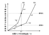
- FIG. 6 shows the relationship between the coefficient of linear expansion of the two types of ultraviolet curable resins and the glass transition point.
- the horizontal axis of FIG. 6 indicates the heating temperature (° C.) of the metal ink 219.
- the heating temperature C1 is, for example, the sintering temperature at which the metal ink is sintered.
- the vertical axis of FIG. 6 is the expansion amount (ppm) of the resin directly under the circuit wiring 221. For example, the expansion amount of the portion of the insulating layer 218 where the temperature rises most due to sintering.
- the glass transition point is, for example, a temperature at which the temperature changes from a hard state to a soft rubber-like state.
- the first resin material 223 shown in FIG. 6 is an ultraviolet curable resin having a glass transition point Tg1 higher than the heating temperature C1.
- the slope of the graph in FIG. 6 indicates the coefficient of linear expansion.
- the second linear expansion coefficient ⁇ 2 of the first resin material 223 having a glass transition point Tg1 or more is sharply larger than the first linear expansion coefficient ⁇ 1 of the first resin material 223 having a glass transition point Tg1 or less.
- the second resin material 225 is an ultraviolet curable resin having a glass transition point Tg2 lower than the heating temperature C1. Similar to the first resin material 223, the second linear expansion coefficient ⁇ 4 of the second resin material 225 having a glass transition point Tg1 or more is higher than the first linear expansion coefficient ⁇ 3 of the second resin material 225 having a glass transition point Tg1 or less. It is growing rapidly.
- Factors that affect the swelling of the circuit wiring 221 include the above-mentioned heating temperature C1, linear expansion coefficient ( ⁇ 1, etc.), glass transition point (Tg1, Tg2), and the interior of the room where the stacking unit forming device 10 is installed. There are various factors such as temperature. As a result of various simulations and experiments, the applicant has found that the swelling and cracking of the circuit wiring 221 can be suppressed extremely effectively by setting the following conditional expression.
- the heating temperature C1 When the heating temperature C1 ⁇ the glass transition point Tg1 When a resin material having a glass transition point Tg1 higher than the heating temperature C1 such as the first resin material 223 is used, the heating temperature C1 satisfying the following equation is used. Thereby, the swelling of the circuit wiring 221 and the like can be effectively suppressed.
- the room temperature of the formula 1 is the temperature of the room in which the stacking unit forming device 10 is installed. That is, the room temperature is the temperature of the environment in which the circuit wiring 221 is modeled.
- the upper limit value is a value indicating the upper limit of expansion of the insulating layer 218 due to heating in the circuit wiring forming step, and is preferably 6000 ppm, for example.
- the upper limit value can be set to a value that is the upper limit of the expansion of the insulating layer 218 that does not cause swelling or cracking in the circuit wiring 221 to be manufactured. More specifically, it can be set by performing a simulation or manufacturing a prototype in advance and measuring the expansion coefficient of the insulating layer 218 when the circuit wiring 221 is swelled or cracked. Alternatively, even if swelling or cracking occurs, the upper limit of swelling of the insulating layer 218 in a range in which the circuit wiring 221 satisfies the desired performance (resistance value or high frequency characteristic) may be set as the upper limit value. That is, an upper limit value in a range that allows fine swelling or cracking may be set.
- the upper limit value can be set to an appropriate value according to the type of resin material used, the type of metal ink, the structure of the laminating unit, and the like.
- the upper limit value is changed according to the stretchability of the metal ink 219, the rigidity of the ultraviolet curable resin, and the like.
- the upper limit value in the present embodiment is the amount of expansion in which the insulating layer 218 (an example of the resin member of the present disclosure) expands due to heating in the circuit wiring forming step, and is a range in which the circuit wiring 221 does not expand or crack.
- the amount of expansion indicating the upper limit of can be set.
- the circuit wiring 221 can be heated within a range in which swelling and cracking do not occur, and the circuit wiring 221 satisfying the desired electrical characteristics can be manufactured by the three-dimensional laminated molding.
- the controller 120 of the present embodiment heats in the circuit wiring forming step at the heating temperature C1 satisfying the above equation 1.
- the resin material a material having a glass transition point Tg1 higher than the heating temperature C1 forming the circuit wiring 221 is adopted. Then, by using the heating temperature C1 satisfying the above (Equation 1), the expansion of the insulating layer 218 can be suppressed, and the expansion and cracking of the circuit wiring 221 can be suppressed.
- the first linear expansion coefficient ⁇ 1 of the ultraviolet curable resin (first resin material 223) used for modeling the insulating layer 218 and the heating temperature C1 according to the room temperature of the use environment are set in advance. It is set.
- the controller 120 controls the current value to be passed through the infrared heater of the irradiation device 78, for example, with the heating temperature C1 as the target temperature.
- the irradiation device 78 may be provided with a temperature sensor for measuring the temperature of the insulating layer 218, and the controller 120 may execute feedback control based on the detection temperature of the temperature sensor and the target temperature.
- the heating temperature C1 can be controlled by the controller 120, and swelling of the circuit wiring 221 can be suppressed.
- the laminated unit forming device 10 may include a temperature sensor for measuring room temperature. Then, the controller 120 may automatically set the heating temperature C1 based on the room temperature and the first line expansion coefficient ⁇ 1 detected by the temperature sensor. Further, the controller 120 may control other factors that affect the swelling of the circuit wiring 221 and the like. For example, the controller 120 may control the distance between the irradiation device 78 and the metal ink 219 and the heating time to suppress the temperature rise of the insulating layer 218.
- the upper limit value is a value indicating the upper limit of expansion of the insulating layer 218 due to heating in the circuit wiring forming step, and is preferably 6000 ppm, for example.
- the upper limit value of (Equation 2) can be set to an appropriate value according to the type of resin material to be used and the like, similarly to the upper limit value of (Equation 1) described above. Further, the upper limit value of (Equation 1) and the upper limit value of (Equation 2) may be different values.
- the controller 120 of the present embodiment heats in the circuit wiring forming step at the heating temperature C1 satisfying the above equation 2.
- the resin material a material whose glass transition point Tg2 is lower than the heating temperature C1 forming the circuit wiring 221 is adopted. Then, by using the heating temperature C1 satisfying the above (Equation 2), the expansion of the insulating layer 218 can be suppressed, and the expansion and cracking of the circuit wiring 221 can be suppressed.
- the controller 120 can control the infrared heater of the irradiation device 78 and control the heating temperature C1 according to the target temperature set in the control program 126, as in the case of (2-1) described above. Further, as described above, in a general resin material, the coefficient of linear expansion sharply increases due to the start of softening in a state above the glass transition point. Therefore, even in the case of an ultraviolet curable resin in which the heating temperature C1> the glass transition point Tg2, the upper limit of the above (Equation 2) is increased in order to secure the heating temperature C1 required for firing the metal ink. It may be necessary to do so. In such a case, the controller 120 of the present embodiment can drive the cooling device 66 (see FIG. 2) to cool the base material 70 and effectively suppress the occurrence of swelling and cracking of the circuit wiring 221.
- the controller 120 may drive the cooling device 66 to cool the base material 70 and suppress the temperature rise of the insulating layer 218. According to this, the temperature rise of the insulating layer 218 can be suppressed, and the expansion of the insulating layer 218 can be suppressed. In particular, when the glass transition point Tg2 is lower than the heating temperature C1, the expansion of the insulating layer 218 due to heating can be suppressed, and the expansion and cracking of the circuit wiring 221 can be effectively suppressed.
- the controller 120 may also be cooled by the cooling device 66 even in the case of the first resin material 223 having the heating temperature C1 ⁇ glass transition point Tg1 described in (2-1) described above.
- the controller 120 does not have to perform cooling by the cooling device 66 in the case of the second resin material 225 having a heating temperature C1 ⁇ glass transition point Tg2.
- the ejection step of FIG. 4 for ejecting the metal ink 219 onto the insulating layer 218 and the top of the insulating layer 218 includes the circuit wiring forming step of FIG. 5 in which the metal ink 219 discharged to the above is heated at a heating temperature C1 and cured to form a circuit wiring 221. Then, in the circuit wiring forming step of FIG. 5, the glass transition points Tg1 and Tg2 of the ultraviolet curable resin, the first line expansion coefficient ⁇ 1, the first line expansion coefficient ⁇ 3, the second line expansion coefficient ⁇ 4, and the heating temperature C1 based on room temperature Heat with.
- the coefficient of linear expansion of the resin material changes significantly before and after the glass transition points Tg1 and Tg2 where softening is started.
- the coefficient of linear expansion of glass transition points Tg1, Tg2 or more becomes the linear expansion coefficient of glass transition point Tg1, Tg2 or less (first linear expansion coefficient ⁇ 1, ⁇ 3). In comparison, it grows sharply.
- factors that affect the cracking and swelling of the circuit wiring 221 include glass transition points Tg1 and Tg2, a coefficient of linear expansion, room temperature, and a heating temperature C1 of the metal ink 219. Therefore, heating is performed using the glass transition points Tg1 and Tg2, the coefficient of linear expansion, and the heating temperature C1 based on room temperature.
- the expansion of the insulating layer 218 due to heating in the circuit wiring forming step can be suppressed to a desired upper limit or less, and the expansion or cracking of the circuit wiring 221 can be suppressed.
- the first resin material 223 and the second resin material 225 are examples of resin materials.
- the insulating layer 218 is an example of a resin member.
- the metal ink 219 is an example of a fluid containing metal particles.
- the resin constituting the insulating layer 218 is not limited to the ultraviolet curable resin, and may be, for example, a thermoplastic resin or a thermosetting resin.
- the laminated unit forming apparatus 10 forms an insulating layer 218 obtained by curing an ultraviolet curable resin as the resin material of the present disclosure by three-dimensional laminated molding.
- the laminated unit forming apparatus 10 may form the circuit wiring 221 on the resin material formed by a method other than the three-dimensional laminated molding (injection molding or the like).
- the configuration of the laminated unit forming device 10 described above is an example, and can be changed as appropriate.
- the laminated unit forming device 10 does not have to include a mounting unit 26 or a mounting portion 102 for mounting electronic components. Further, the laminated unit forming device 10 does not have to include the cooling device 66. Further, in the above embodiment, the laminated unit forming apparatus 10 has a configuration capable of performing modeling with two types of resins, the first resin material 223 and the second resin material 225, but modeling of only one of the resins. The configuration may be such that
- Base material Insulation layer (resin material) 219 Metal ink (fluid containing metal particles) 221 Circuit wiring 223 1st resin material (resin material) 225 Second resin material (resin material) Tg1, Tg2 Glass transition point ⁇ 1 1st line expansion coefficient ⁇ 2 2nd line expansion coefficient ⁇ 3 1st line expansion coefficient ⁇ 4 2nd line expansion coefficient
Landscapes
- Engineering & Computer Science (AREA)
- Manufacturing & Machinery (AREA)
- Chemical & Material Sciences (AREA)
- Microelectronics & Electronic Packaging (AREA)
- Materials Engineering (AREA)
- Optics & Photonics (AREA)
- Mechanical Engineering (AREA)
- Physics & Mathematics (AREA)
- Ceramic Engineering (AREA)
- Civil Engineering (AREA)
- Composite Materials (AREA)
- Structural Engineering (AREA)
- Manufacturing Of Printed Wiring (AREA)
Priority Applications (4)
| Application Number | Priority Date | Filing Date | Title |
|---|---|---|---|
| PCT/JP2019/029943 WO2021019707A1 (ja) | 2019-07-31 | 2019-07-31 | 3次元積層造形による回路配線の製造方法 |
| JP2021536532A JP7344297B2 (ja) | 2019-07-31 | 2019-07-31 | 3次元積層造形による回路配線の製造方法 |
| EP19939422.2A EP4007458B1 (en) | 2019-07-31 | 2019-07-31 | Method for manufacturing circuit wiring by three-dimensional additive manufacturing |
| US17/630,831 US12550268B2 (en) | 2019-07-31 | 2019-07-31 | Method for manufacturing circuit wiring by three-dimensional additive manufacturing |
Applications Claiming Priority (1)
| Application Number | Priority Date | Filing Date | Title |
|---|---|---|---|
| PCT/JP2019/029943 WO2021019707A1 (ja) | 2019-07-31 | 2019-07-31 | 3次元積層造形による回路配線の製造方法 |
Publications (1)
| Publication Number | Publication Date |
|---|---|
| WO2021019707A1 true WO2021019707A1 (ja) | 2021-02-04 |
Family
ID=74228378
Family Applications (1)
| Application Number | Title | Priority Date | Filing Date |
|---|---|---|---|
| PCT/JP2019/029943 Ceased WO2021019707A1 (ja) | 2019-07-31 | 2019-07-31 | 3次元積層造形による回路配線の製造方法 |
Country Status (4)
| Country | Link |
|---|---|
| US (1) | US12550268B2 (https=) |
| EP (1) | EP4007458B1 (https=) |
| JP (1) | JP7344297B2 (https=) |
| WO (1) | WO2021019707A1 (https=) |
Cited By (1)
| Publication number | Priority date | Publication date | Assignee | Title |
|---|---|---|---|---|
| JP7768443B1 (ja) * | 2025-03-21 | 2025-11-12 | 住友ベークライト株式会社 | 積層体、及び積層体の製造方法 |
Citations (5)
| Publication number | Priority date | Publication date | Assignee | Title |
|---|---|---|---|---|
| US20100055302A1 (en) * | 2008-09-04 | 2010-03-04 | Samsung Electro-Mechanics Co., Ltd. | Reducing agent for low temperature reducing and sintering of copper nanoparticles, and method for low temperature sintering using the same |
| WO2013182896A1 (en) * | 2012-06-05 | 2013-12-12 | Showa Denko K.K. | Substrate film and sintering method |
| JP2017183645A (ja) * | 2016-03-31 | 2017-10-05 | コニカミノルタ株式会社 | 三次元造形物の製造方法 |
| WO2017221347A1 (ja) * | 2016-06-22 | 2017-12-28 | 富士機械製造株式会社 | 回路形成方法、および回路形成装置 |
| WO2019102522A1 (ja) | 2017-11-21 | 2019-05-31 | 株式会社Fuji | 3次元積層電子デバイスの製造方法及び3次元積層電子デバイス |
Family Cites Families (6)
| Publication number | Priority date | Publication date | Assignee | Title |
|---|---|---|---|---|
| US20070281091A1 (en) * | 2006-05-31 | 2007-12-06 | Cabot Corporation | Polyimide insulative layers in multi-layered printed electronic features |
| US8008767B2 (en) * | 2006-09-13 | 2011-08-30 | Sumitomo Bakelight Co., Ltd. | Semiconductor device |
| JP4983811B2 (ja) * | 2009-01-09 | 2012-07-25 | 日立電線株式会社 | 導電性回路形成方法および導電回路装置 |
| JP5405391B2 (ja) * | 2010-05-21 | 2014-02-05 | 日本メクトロン株式会社 | 透明フレキシブルプリント配線板及びその製造方法 |
| JP6099524B2 (ja) * | 2013-08-30 | 2017-03-22 | 富士フイルム株式会社 | バリア性積層体、ガスバリアフィルム、およびその応用 |
| US10667403B2 (en) * | 2014-09-19 | 2020-05-26 | Fuji Corporation | Manufacturing apparatus for performing additive manufacturing of an electrical device |
-
2019
- 2019-07-31 JP JP2021536532A patent/JP7344297B2/ja active Active
- 2019-07-31 WO PCT/JP2019/029943 patent/WO2021019707A1/ja not_active Ceased
- 2019-07-31 US US17/630,831 patent/US12550268B2/en active Active
- 2019-07-31 EP EP19939422.2A patent/EP4007458B1/en active Active
Patent Citations (5)
| Publication number | Priority date | Publication date | Assignee | Title |
|---|---|---|---|---|
| US20100055302A1 (en) * | 2008-09-04 | 2010-03-04 | Samsung Electro-Mechanics Co., Ltd. | Reducing agent for low temperature reducing and sintering of copper nanoparticles, and method for low temperature sintering using the same |
| WO2013182896A1 (en) * | 2012-06-05 | 2013-12-12 | Showa Denko K.K. | Substrate film and sintering method |
| JP2017183645A (ja) * | 2016-03-31 | 2017-10-05 | コニカミノルタ株式会社 | 三次元造形物の製造方法 |
| WO2017221347A1 (ja) * | 2016-06-22 | 2017-12-28 | 富士機械製造株式会社 | 回路形成方法、および回路形成装置 |
| WO2019102522A1 (ja) | 2017-11-21 | 2019-05-31 | 株式会社Fuji | 3次元積層電子デバイスの製造方法及び3次元積層電子デバイス |
Cited By (1)
| Publication number | Priority date | Publication date | Assignee | Title |
|---|---|---|---|---|
| JP7768443B1 (ja) * | 2025-03-21 | 2025-11-12 | 住友ベークライト株式会社 | 積層体、及び積層体の製造方法 |
Also Published As
| Publication number | Publication date |
|---|---|
| US12550268B2 (en) | 2026-02-10 |
| EP4007458B1 (en) | 2023-08-09 |
| EP4007458A4 (en) | 2022-08-10 |
| JP7344297B2 (ja) | 2023-09-13 |
| US20220279658A1 (en) | 2022-09-01 |
| EP4007458A1 (en) | 2022-06-01 |
| JPWO2021019707A1 (https=) | 2021-02-04 |
Similar Documents
| Publication | Publication Date | Title |
|---|---|---|
| JP6947842B2 (ja) | 3次元積層電子デバイスの製造方法 | |
| JP7316742B2 (ja) | 3次元積層造形による実装基板の製造方法 | |
| WO2017212567A1 (ja) | 回路形成方法 | |
| JP6554541B2 (ja) | 配線形成方法および配線形成装置 | |
| JP7055897B2 (ja) | 回路形成方法 | |
| JP6533112B2 (ja) | 回路形成方法 | |
| JPWO2019193644A1 (ja) | 3次元構造物形成方法、および3次元構造物形成装置 | |
| WO2021019707A1 (ja) | 3次元積層造形による回路配線の製造方法 | |
| CN116438080B (zh) | 三维造型物的制造方法及制造装置 | |
| JPWO2016189577A1 (ja) | 配線形成方法 | |
| JP6949751B2 (ja) | 3次元積層造形のビア形成方法 | |
| JP7325532B2 (ja) | 積層造形法による3次元造形物の製造方法及び3次元造形物製造装置 | |
| JP7394626B2 (ja) | 3次元積層電子デバイスの製造方法及び製造装置 | |
| WO2021166139A1 (ja) | 回路形成方法 | |
| JP2022029021A (ja) | 治具の製造方法、治具、3次元造形物製造装置、及び3次元造形物の製造方法 | |
| JP7142781B2 (ja) | 配線基板の製造方法及び配線基板製造装置 | |
| JPWO2019186780A1 (ja) | 回路形成方法、および回路形成装置 | |
| JP6967138B2 (ja) | キャビティの形成方法 | |
| WO2023223562A1 (ja) | 製造方法及び製造装置 | |
| JP2022079926A (ja) | 造形方法及び造形装置 | |
| JP2023166848A (ja) | 電気回路形成方法、および電気回路形成装置 | |
| WO2023209960A1 (ja) | 設計方法、設計プログラム、および回路基板作製方法 | |
| WO2022101965A1 (ja) | 回路形成方法 |
Legal Events
| Date | Code | Title | Description |
|---|---|---|---|
| 121 | Ep: the epo has been informed by wipo that ep was designated in this application |
Ref document number: 19939422 Country of ref document: EP Kind code of ref document: A1 |
|
| ENP | Entry into the national phase |
Ref document number: 2021536532 Country of ref document: JP Kind code of ref document: A |
|
| NENP | Non-entry into the national phase |
Ref country code: DE |
|
| ENP | Entry into the national phase |
Ref document number: 2019939422 Country of ref document: EP Effective date: 20220228 |
|
| WWG | Wipo information: grant in national office |
Ref document number: 17630831 Country of ref document: US |