EP4007458B1 - Method for manufacturing circuit wiring by three-dimensional additive manufacturing - Google Patents
Method for manufacturing circuit wiring by three-dimensional additive manufacturing Download PDFInfo
- Publication number
- EP4007458B1 EP4007458B1 EP19939422.2A EP19939422A EP4007458B1 EP 4007458 B1 EP4007458 B1 EP 4007458B1 EP 19939422 A EP19939422 A EP 19939422A EP 4007458 B1 EP4007458 B1 EP 4007458B1
- Authority
- EP
- European Patent Office
- Prior art keywords
- circuit wiring
- heating
- linear expansion
- expansion coefficient
- glass transition
- Prior art date
- Legal status (The legal status is an assumption and is not a legal conclusion. Google has not performed a legal analysis and makes no representation as to the accuracy of the status listed.)
- Active
Links
Images


Classifications
-
- H—ELECTRICITY
- H05—ELECTRIC TECHNIQUES NOT OTHERWISE PROVIDED FOR
- H05K—PRINTED CIRCUITS; CASINGS OR CONSTRUCTIONAL DETAILS OF ELECTRIC APPARATUS; MANUFACTURE OF ASSEMBLAGES OF ELECTRICAL COMPONENTS
- H05K3/00—Apparatus or processes for manufacturing printed circuits
- H05K3/10—Apparatus or processes for manufacturing printed circuits in which conductive material is applied to the insulating support in such a manner as to form the desired conductive pattern
- H05K3/12—Apparatus or processes for manufacturing printed circuits in which conductive material is applied to the insulating support in such a manner as to form the desired conductive pattern using thick film techniques, e.g. printing techniques to apply the conductive material or similar techniques for applying conductive paste or ink patterns
- H05K3/1275—Apparatus or processes for manufacturing printed circuits in which conductive material is applied to the insulating support in such a manner as to form the desired conductive pattern using thick film techniques, e.g. printing techniques to apply the conductive material or similar techniques for applying conductive paste or ink patterns by other printing techniques, e.g. letterpress printing, intaglio printing, lithographic printing, offset printing
-
- B—PERFORMING OPERATIONS; TRANSPORTING
- B29—WORKING OF PLASTICS; WORKING OF SUBSTANCES IN A PLASTIC STATE IN GENERAL
- B29C—SHAPING OR JOINING OF PLASTICS; SHAPING OF MATERIAL IN A PLASTIC STATE, NOT OTHERWISE PROVIDED FOR; AFTER-TREATMENT OF THE SHAPED PRODUCTS, e.g. REPAIRING
- B29C64/00—Additive manufacturing, i.e. manufacturing of three-dimensional [3D] objects by additive deposition, additive agglomeration or additive layering, e.g. by 3D printing, stereolithography or selective laser sintering
- B29C64/10—Processes of additive manufacturing
- B29C64/106—Processes of additive manufacturing using only liquids or viscous materials, e.g. depositing a continuous bead of viscous material
-
- B—PERFORMING OPERATIONS; TRANSPORTING
- B22—CASTING; POWDER METALLURGY
- B22F—WORKING METALLIC POWDER; MANUFACTURE OF ARTICLES FROM METALLIC POWDER; MAKING METALLIC POWDER; APPARATUS OR DEVICES SPECIALLY ADAPTED FOR METALLIC POWDER
- B22F1/00—Metallic powder; Treatment of metallic powder, e.g. to facilitate working or to improve properties
- B22F1/10—Metallic powder containing lubricating or binding agents; Metallic powder containing organic material
- B22F1/107—Metallic powder containing lubricating or binding agents; Metallic powder containing organic material containing organic material comprising solvents, e.g. for slip casting
-
- B—PERFORMING OPERATIONS; TRANSPORTING
- B33—ADDITIVE MANUFACTURING TECHNOLOGY
- B33Y—ADDITIVE MANUFACTURING, i.e. MANUFACTURING OF THREE-DIMENSIONAL [3D] OBJECTS BY ADDITIVE DEPOSITION, ADDITIVE AGGLOMERATION OR ADDITIVE LAYERING, e.g. BY 3D PRINTING, STEREOLITHOGRAPHY OR SELECTIVE LASER SINTERING
- B33Y10/00—Processes of additive manufacturing
-
- B—PERFORMING OPERATIONS; TRANSPORTING
- B33—ADDITIVE MANUFACTURING TECHNOLOGY
- B33Y—ADDITIVE MANUFACTURING, i.e. MANUFACTURING OF THREE-DIMENSIONAL [3D] OBJECTS BY ADDITIVE DEPOSITION, ADDITIVE AGGLOMERATION OR ADDITIVE LAYERING, e.g. BY 3D PRINTING, STEREOLITHOGRAPHY OR SELECTIVE LASER SINTERING
- B33Y70/00—Materials specially adapted for additive manufacturing
- B33Y70/10—Composites of different types of material, e.g. mixtures of ceramics and polymers or mixtures of metals and biomaterials
-
- H—ELECTRICITY
- H05—ELECTRIC TECHNIQUES NOT OTHERWISE PROVIDED FOR
- H05K—PRINTED CIRCUITS; CASINGS OR CONSTRUCTIONAL DETAILS OF ELECTRIC APPARATUS; MANUFACTURE OF ASSEMBLAGES OF ELECTRICAL COMPONENTS
- H05K1/00—Printed circuits
- H05K1/02—Details
- H05K1/03—Use of materials for the substrate
-
- H—ELECTRICITY
- H05—ELECTRIC TECHNIQUES NOT OTHERWISE PROVIDED FOR
- H05K—PRINTED CIRCUITS; CASINGS OR CONSTRUCTIONAL DETAILS OF ELECTRIC APPARATUS; MANUFACTURE OF ASSEMBLAGES OF ELECTRICAL COMPONENTS
- H05K3/00—Apparatus or processes for manufacturing printed circuits
- H05K3/10—Apparatus or processes for manufacturing printed circuits in which conductive material is applied to the insulating support in such a manner as to form the desired conductive pattern
- H05K3/12—Apparatus or processes for manufacturing printed circuits in which conductive material is applied to the insulating support in such a manner as to form the desired conductive pattern using thick film techniques, e.g. printing techniques to apply the conductive material or similar techniques for applying conductive paste or ink patterns
- H05K3/1241—Apparatus or processes for manufacturing printed circuits in which conductive material is applied to the insulating support in such a manner as to form the desired conductive pattern using thick film techniques, e.g. printing techniques to apply the conductive material or similar techniques for applying conductive paste or ink patterns by ink-jet printing or drawing by dispensing
- H05K3/125—Apparatus or processes for manufacturing printed circuits in which conductive material is applied to the insulating support in such a manner as to form the desired conductive pattern using thick film techniques, e.g. printing techniques to apply the conductive material or similar techniques for applying conductive paste or ink patterns by ink-jet printing or drawing by dispensing by ink-jet printing
-
- H—ELECTRICITY
- H05—ELECTRIC TECHNIQUES NOT OTHERWISE PROVIDED FOR
- H05K—PRINTED CIRCUITS; CASINGS OR CONSTRUCTIONAL DETAILS OF ELECTRIC APPARATUS; MANUFACTURE OF ASSEMBLAGES OF ELECTRICAL COMPONENTS
- H05K3/00—Apparatus or processes for manufacturing printed circuits
- H05K3/46—Manufacturing multilayer circuits
- H05K3/4644—Manufacturing multilayer circuits by building the multilayer layer by layer, i.e. build-up multilayer circuits
-
- B—PERFORMING OPERATIONS; TRANSPORTING
- B22—CASTING; POWDER METALLURGY
- B22F—WORKING METALLIC POWDER; MANUFACTURE OF ARTICLES FROM METALLIC POWDER; MAKING METALLIC POWDER; APPARATUS OR DEVICES SPECIALLY ADAPTED FOR METALLIC POWDER
- B22F10/00—Additive manufacturing of workpieces or articles from metallic powder
- B22F10/20—Direct sintering or melting
- B22F10/25—Direct deposition of metal particles, e.g. direct metal deposition [DMD] or laser engineered net shaping [LENS]
-
- B—PERFORMING OPERATIONS; TRANSPORTING
- B29—WORKING OF PLASTICS; WORKING OF SUBSTANCES IN A PLASTIC STATE IN GENERAL
- B29L—INDEXING SCHEME ASSOCIATED WITH SUBCLASS B29C, RELATING TO PARTICULAR ARTICLES
- B29L2031/00—Other particular articles
- B29L2031/34—Electrical apparatus, e.g. sparking plugs or parts thereof
- B29L2031/3425—Printed circuits
-
- B—PERFORMING OPERATIONS; TRANSPORTING
- B33—ADDITIVE MANUFACTURING TECHNOLOGY
- B33Y—ADDITIVE MANUFACTURING, i.e. MANUFACTURING OF THREE-DIMENSIONAL [3D] OBJECTS BY ADDITIVE DEPOSITION, ADDITIVE AGGLOMERATION OR ADDITIVE LAYERING, e.g. BY 3D PRINTING, STEREOLITHOGRAPHY OR SELECTIVE LASER SINTERING
- B33Y80/00—Products made by additive manufacturing
-
- H—ELECTRICITY
- H05—ELECTRIC TECHNIQUES NOT OTHERWISE PROVIDED FOR
- H05K—PRINTED CIRCUITS; CASINGS OR CONSTRUCTIONAL DETAILS OF ELECTRIC APPARATUS; MANUFACTURE OF ASSEMBLAGES OF ELECTRICAL COMPONENTS
- H05K2201/00—Indexing scheme relating to printed circuits covered by H05K1/00
- H05K2201/06—Thermal details
- H05K2201/068—Thermal details wherein the coefficient of thermal expansion is important
-
- H—ELECTRICITY
- H05—ELECTRIC TECHNIQUES NOT OTHERWISE PROVIDED FOR
- H05K—PRINTED CIRCUITS; CASINGS OR CONSTRUCTIONAL DETAILS OF ELECTRIC APPARATUS; MANUFACTURE OF ASSEMBLAGES OF ELECTRICAL COMPONENTS
- H05K2203/00—Indexing scheme relating to apparatus or processes for manufacturing printed circuits covered by H05K3/00
- H05K2203/01—Tools for processing; Objects used during processing
- H05K2203/0104—Tools for processing; Objects used during processing for patterning or coating
- H05K2203/013—Inkjet printing, e.g. for printing insulating material or resist
-
- H—ELECTRICITY
- H05—ELECTRIC TECHNIQUES NOT OTHERWISE PROVIDED FOR
- H05K—PRINTED CIRCUITS; CASINGS OR CONSTRUCTIONAL DETAILS OF ELECTRIC APPARATUS; MANUFACTURE OF ASSEMBLAGES OF ELECTRICAL COMPONENTS
- H05K2203/00—Indexing scheme relating to apparatus or processes for manufacturing printed circuits covered by H05K3/00
- H05K2203/11—Treatments characterised by their effect, e.g. heating, cooling, roughening
- H05K2203/1131—Sintering, i.e. fusing of metal particles to achieve or improve electrical conductivity
-
- H—ELECTRICITY
- H05—ELECTRIC TECHNIQUES NOT OTHERWISE PROVIDED FOR
- H05K—PRINTED CIRCUITS; CASINGS OR CONSTRUCTIONAL DETAILS OF ELECTRIC APPARATUS; MANUFACTURE OF ASSEMBLAGES OF ELECTRICAL COMPONENTS
- H05K3/00—Apparatus or processes for manufacturing printed circuits
- H05K3/10—Apparatus or processes for manufacturing printed circuits in which conductive material is applied to the insulating support in such a manner as to form the desired conductive pattern
- H05K3/12—Apparatus or processes for manufacturing printed circuits in which conductive material is applied to the insulating support in such a manner as to form the desired conductive pattern using thick film techniques, e.g. printing techniques to apply the conductive material or similar techniques for applying conductive paste or ink patterns
- H05K3/1283—After-treatment of the printed patterns, e.g. sintering or curing methods
-
- H—ELECTRICITY
- H05—ELECTRIC TECHNIQUES NOT OTHERWISE PROVIDED FOR
- H05K—PRINTED CIRCUITS; CASINGS OR CONSTRUCTIONAL DETAILS OF ELECTRIC APPARATUS; MANUFACTURE OF ASSEMBLAGES OF ELECTRICAL COMPONENTS
- H05K3/00—Apparatus or processes for manufacturing printed circuits
- H05K3/46—Manufacturing multilayer circuits
- H05K3/4644—Manufacturing multilayer circuits by building the multilayer layer by layer, i.e. build-up multilayer circuits
- H05K3/4673—Application methods or materials of intermediate insulating layers not specially adapted to any one of the previous methods of adding a circuit layer
-
- Y—GENERAL TAGGING OF NEW TECHNOLOGICAL DEVELOPMENTS; GENERAL TAGGING OF CROSS-SECTIONAL TECHNOLOGIES SPANNING OVER SEVERAL SECTIONS OF THE IPC; TECHNICAL SUBJECTS COVERED BY FORMER USPC CROSS-REFERENCE ART COLLECTIONS [XRACs] AND DIGESTS
- Y02—TECHNOLOGIES OR APPLICATIONS FOR MITIGATION OR ADAPTATION AGAINST CLIMATE CHANGE
- Y02P—CLIMATE CHANGE MITIGATION TECHNOLOGIES IN THE PRODUCTION OR PROCESSING OF GOODS
- Y02P10/00—Technologies related to metal processing
- Y02P10/25—Process efficiency
Definitions
- the present disclosure relates to a method for manufacturing a circuit wiring by three-dimensional additive manufacturing.
- Patent Literature 1 discloses a technique of forming a laminate unit including an electronic component and a circuit wiring by three-dimensional additive manufacturing.
- an insulating layer is formed by discharging an ultraviolet curable resin onto a base material and curing the resin.
- Patent Literature 2 discloses methods for manufacturing a circuit wiring by three-dimensional additive manufacturing according to the preambles of independent claims 1 and 2.
- the present disclosure has been made in view of the above-described points, and an object thereof is to provide a method for manufacturing a circuit wiring by three-dimensional additive manufacturing capable of suppressing swelling and cracking of the circuit wiring in a case where the circuit wiring is formed on a resin member by three-dimensional additive manufacturing.
- the object is achieved with a method for manufacturing a circuit wiring by three-dimensional additive manufacturing according to independent claim 1, and with a method for manufacturing a circuit wiring by three-dimensional additive manufacturing according to independent claim 2.
- Preferred embodiments are set out in the dependent claims.
- the linear expansion coefficient of the resin material significantly changes before and after the glass transition point at which softening is initiated. Normally, the linear expansion coefficient equal to or higher than the glass transition point is rapidly increased as compared with the linear expansion coefficient equal to or lower than the glass transition point.
- the glass transition point of the resin material forming the resin member there are the glass transition point of the resin material forming the resin member, the linear expansion coefficient, the room temperature, and the heating temperature for heating the fluid containing the metal particle. Therefore, heating is performed using the heating temperature based on the glass transition point, the linear expansion coefficient, and the room temperature. As a result, the expansion of the resin member due to the heating in the circuit wiring forming step can be suppressed to a desired upper limit or lower, and swelling or cracking of the circuit wiring can be suppressed.
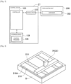
- Fig. 1 illustrates laminate unit forming device 10.
- Laminate unit forming device 10 is provided with conveyance device 20, first shaping unit 22, second shaping unit 24, mounting unit 26, third shaping unit 200, and control device 27 (refer to Figs. 2 and 3 ).
- Conveyance device 20, first shaping unit 22, second shaping unit 24, mounting unit 26, and third shaping unit 200 are disposed on base 28 of laminate unit forming device 10.
- Base 28 has normally rectangular in a plan view.
- a longitudinal direction of base 28 will be referred to as an X-axis direction
- a shorter direction of base 28 will be referred to as a Y-axis direction
- a direction orthogonal to both of the X-axis direction and the Y-axis direction will be referred to as a Z-axis direction.
- Conveyance device 20 is provided with X-axis slide mechanism 30 and Y-axis slide mechanism 32.
- X-axis slide mechanism 30 includes X-axis slide rail 34 and X-axis slider 36.
- X-axis slide rail 34 is disposed to extend in the X-axis direction on base 28.
- X-axis slider 36 is held by X-axis slide rail 34 to be slidable in the X-axis direction.
- X-axis slide mechanism 30 includes electromagnetic motor 38 (refer to Fig. 2 ) and moves X-axis slider 36 to any position in the X-axis direction by driving electromagnetic motor 38.
- Y-axis slide mechanism 32 includes Y-axis slide rail 50 and stage 52.
- Y-axis slide rail 50 is disposed to extend in the Y-axis direction on base 28.
- One end portion of Y-axis slide rail 50 is connected to X-axis slider 36. Therefore, Y-axis slide rail 50 is movable in the X-axis direction.
- Stage 52 is held by Y-axis slide rail 50 so as to be slidable in the Y-axis direction.
- Y-axis slide mechanism 32 includes electromagnetic motor 56 (refer to Fig. 2 ) and moves stage 52 to any position in the Y-axis direction by driving electromagnetic motor 56. As a result, by driving X-axis slide mechanism 30 and Y-axis slide mechanism 32, stage 52 is moved to any position on base 28.
- Stage 52 includes base plate 60, holding device 62, lifting and lowering device 64, and cooling device 66.
- Base plate 60 is formed in a flat plate shape, and base material 70 (refer to Fig. 4 ) is placed on an upper surface thereof.
- Holding device 62 is provided on both side portions of base plate 60 in the X-axis direction. Holding device 62 fixedly holds base material 70 with respect to base plate 60 by interposing both edge portions in the X-axis direction of base material 70 placed on base plate 60.
- lifting and lowering device 64 is disposed below base plate 60, and lifts and lowers base plate 60 in the Z-axis direction.
- cooling device 66 is a device for cooling base material 70 placed on base plate 60.
- the configuration of cooling device 66 is not particularly limited, and, for example, a gas cooling device using gas as a refrigerant, a liquid cooling device using liquid as a refrigerant, a device using a heat pipe, or the like can be employed. Cooling device 66 is driven based on the control of control device 27 (refer to Fig. 2 ) to cool base material 70, and thus the shaped object formed on base material 70 is cooled.
- First shaping unit 22 is a unit for shaping a circuit wiring on base material 70 placed on base plate 60 of stage 52, and includes first printing section 72 and firing section 74.
- First printing section 72 includes ink jet head 76 (refer to Fig. 2 ) and linearly discharges metal ink onto base material 70 placed on base plate 60.
- the metal ink is an example of a fluid containing metal particles of the present disclosure.
- the metal ink is, for example, one in which fine particles of a metal (such as silver) having a nanometer size are dispersed in a solvent, and is cured by firing with heat.
- the surface of the metal fine particle is coated with, for example, a dispersant to suppress aggregation in the solvent.
- Ink jet head 76 discharges the metal ink from multiple nozzles, for example by a piezo method using a piezoelectric element.
- the device for discharging a fluid containing metal particles is not limited to an ink jet head including multiple nozzles, and may be, for example, a dispenser including one nozzle.
- the type of metal included in the metal ink is not limited to silver, and may be copper, gold, or the like.
- the number of types of metals included in the metal ink is not limited to one type, and may be multiple types.
- Firing section 74 includes irradiation device 78 (refer to Fig. 2 ).
- Irradiation device 78 is provided with, for example, an infrared heater that heats the metal ink discharged onto base material 70.
- the metal ink is fired by applying heat from the infrared heater to form a circuit wiring.
- the firing of the metal ink referred to herein means, for example, a phenomenon in which by applying energy, a solvent is vaporized or a protective film of the metal fine particles, that is, a dispersant is decomposed, and the metal fine particles are brought into contact with each other or fused to increase the conductivity.
- a circuit wiring can be formed by firing the metal ink.
- the device for heating the metal ink is not limited to the infrared heater.
- laminate unit forming device 10 may be provided with an infrared lamp, a laser irradiation device that irradiates the metal ink with laser light, or an electric furnace in which base material 70 from which the metal ink is discharged is placed in a furnace and heated as a device for heating the metal ink.
- the temperature at which the metal ink is heated is not limited to, for example, the temperature of firing lower than the melting point of the metal included in the metal ink, and may be the temperature higher than the melting point of the metal.
- second shaping unit 24 is a unit for shaping an insulating layer (one example of the resin member of the present disclosure) on base material 70 placed on base plate 60, and includes second printing section 84 and curing section 86.
- Second printing section 84 includes ink jet head 88 (refer to Fig. 2 ), and discharges an ultraviolet curable resin onto base material 70 placed on base plate 60.
- the ultraviolet curable resin is a resin that is cured by irradiation with ultraviolet rays.
- a method by which ink jet head 88 discharges the ultraviolet curable resin may be, for example, a piezo method using a piezoelectric element, or may be a thermal method in which the resin is heated to generate air bubbles and discharged from multiple nozzles.
- Curing section 86 includes flattening device 90 (refer to Fig. 2 ) and irradiation device 92 (refer to Fig. 2 ).
- Flattening device 90 is a device for flattening an upper surface of the ultraviolet curable resin discharged onto base material 70 by inkjet head 88.
- Flattening device 90 makes the thickness of the ultraviolet curable resin uniform, for example, by scraping off excess resin by a roller or a blade while leveling the surface of the ultraviolet curable resin.
- irradiation device 92 is provided with a mercury lamp or LED as a light source, and irradiates the ultraviolet curable resin discharged onto base material 70 with ultraviolet rays. As a result, the ultraviolet curable resin discharged onto base material 70 is cured, and an insulating layer can be formed.
- mounting unit 26 is a unit for mounting an electronic component or a probe pin on base material 70 placed on base plate 60, and includes supply section 100 and mounting section 102.
- Supply section 100 includes multiple tape feeders 110 (refer to Fig. 2 ) for feeding the taped electronic components one by one, and supplies the electronic components at each supply position.
- supply section 100 includes tray 201 (refer to Fig. 2 ) in which probe pins are disposed in a standing state, and supplies the probe pins in a state capable of being picked up from tray 201.
- the electronic component is, for example, a sensor element such as a temperature sensor.
- the probe pin is a member that electrically connects the circuit wirings of one laminate unit and the circuit wirings of other laminate units.
- the supply of the electronic components is not limited to the supply by tape feeder 110, and may be performed by a tray.
- the supply of the probe pins is not limited to the supply by tray 201, and may be performed by a tape feeder.
- the supply of the electronic components and the probe pins may be performed by both the supply by the tape feeder and the supply by the tray, or may be performed by other supplies.
- Mounting section 102 includes mounting head 112 (refer to Fig. 2 ) and moving device 114 (refer to Fig. 2 ).
- Mounting head 112 includes a suction nozzle for picking up and holding an electronic component or a probe pin.
- the suction nozzle picks up and holds the electronic component or the like by suction of air by supplying a negative pressure from a positive and negative pressure supply device (not illustrated).
- the electronic component or the like is separated by supplying a slight positive pressure from the positive and negative pressure supplying device.
- moving device 114 moves mounting head 112 between the supply position of tape feeder 110 or tray 201 and base material 70 placed on base plate 60.
- mounting section 102 holds the electronic component or the like by the suction nozzle, and disposes the electronic component or the like held by the suction nozzle on base material 70.
- Third shaping unit 200 is a unit for discharging a conductive adhesive onto base material 70 placed on base plate 60.
- the conductive adhesive is a conductive paste that is cured by heating, and is used, for example, for forming a through-hole for connecting circuit wirings or for electrically connecting (fixing) terminals of electronic components.
- Third shaping unit 200 includes dispenser 202 (refer to Fig. 3 ) as a device for discharging the conductive adhesive.
- the device for discharging the conductive adhesive or the like is not limited to the dispenser, and may be a screen printing device or a gravure printing device.
- Dispenser 202 discharges a conductive adhesive into the through-hole of the insulating layer, the surface of the insulating layer, or the like.
- the conductive adhesive filled in the through-hole is heated and cured, for example, by firing section 74 of first shaping unit 22, and thus the through-hole is formed.
- the conductive adhesive discharged onto the surface of the insulating layer is heated and cured, for example, by firing section 74, and thus the terminals and the circuit wirings of the electronic components disposed by mounting head 112 are connected to each other.
- control device 27 is provided with controller 120, multiple drive circuits 122, and storage device 124.
- multiple drive circuits 122 are connected to electromagnetic motors 38 and 56, holding device 62, lifting and lowering device 64, cooling device 66, inkjet head 76, irradiation device 78, inkjet head 88, flattening device 90, irradiation device 92, tape feeder 110, mounting head 112, and moving device 114.
- drive circuit 122 is connected to third shaping unit 200 described above.
- Controller 120 is provided with CPU, ROM, RAM, and the like, is mainly a computer, and is connected to multiple drive circuits 122.
- Storage device 124 is provided with RAM, ROM, a hard disk, and the like, and stores control program 126 for controlling laminate unit forming device 10. Controller 120 can control the operations of conveyance device 20, first shaping unit 22, second shaping unit 24, mounting unit 26, third shaping unit 200, and the like by executing control program 126 with CPU. In the following description, the fact that controller 120 executes control program 126 to control each device may be simply referred to as a "device". For example, the fact that “controller 120 moves base plate 60" means that "controller 120 executes control program 126, controls the operation of conveyance device 20 via drive circuit 122, and moves base plate 60 by the operation of conveyance device 20".
- Laminate unit forming device 10 of the present embodiment manufactures a three-dimensional laminate electronic device by shaping multiple laminate units including circuit wirings and electronic components according to the above configuration, and assembling the multiple laminate units. Specifically, controller 120 controls first shaping unit 22 and cures the metal ink to form the circuit wiring. In addition, controller 120 controls second shaping unit 24 and cures the ultraviolet curable resin to form the insulating layer. Controller 120 can form a laminate unit having any shape by changing the shape of the circuit wiring or the insulating layer.
- controller 120 mounts the electronic component by mounting unit 26 in the process of shaping the laminate unit. For example, three-dimensional data of each layer obtained by slicing the laminate unit is set in control program 126. Controller 120 discharges and cures the ultraviolet curable resin based on the data of control program 126 to form a laminate unit. In addition, controller 120 detects information such as a layer or a position where the electronic component is disposed based on the data of control program 126, and mounts the electronic component on the laminate unit based on the detected information. In addition, controller 120 executes the mounting of the probe pin supplied from mounting unit 26 or the shaping with the conductive adhesive discharged from dispenser 202 of third shaping unit 200 on the laminate unit based on the data of control program 126.
- a desired three-dimensional laminate electronic device can be manufactured by assembling the multiple laminate units shaped in this manner.
- the method of fixing multiple laminate units to each other is not particularly limited, and a method using a screw, a bolt, a nut, or the like, or a method using an adhesive can be employed.
- the work for assembling multiple laminate units may be automatically executed by laminate unit forming device 10.
- laminate unit forming device 10 may be provided with a robot arm that assembles and fixes multiple laminate units to each other.
- the work for assembling multiple laminate units may be performed manually by the user.
- Fig. 4 illustrates the discharging step.
- controller 120 controls conveyance device 20 (refer to Fig. 1 ), and moves stage 52 on which base material 70 is set below second shaping unit 24 (refer to Fig. 1 ).
- Controller 120 controls inkjet head 88 of second shaping unit 24 to discharge the ultraviolet curable resin onto base material 70 (one example of the second discharging step of the present disclosure).
- Controller 120 controls irradiation device 92 to irradiate the ultraviolet curable resin discharged onto base material 70 with ultraviolet rays to cure the ultraviolet curable resin (one example of the curing step of the present disclosure). Controller 120 repeatedly executes discharging and curing to form insulating layer 218 (refer to Fig. 4 ) on base material 70 (one example of the insulating layer forming step of the present disclosure).
- controller 120 controls conveyance device 20, and moves stage 52 on which base material 70 is set below first shaping unit 22 (refer to Fig. 1 ). As illustrated in Fig. 4 , controller 120 controls ink jet head 76 of first shaping unit 22 to discharge metal ink 219 in a thin film form onto upper surface 218A of insulating layer 218. Controller 120 discharges metal ink 219 based on three-dimensional data of control program 126 (data of the circuit wiring).
- controller 120 heats and fires metal ink 219 discharged to upper surface 218A by irradiation device 78 of firing section 74.
- controller 120 repeatedly executes the discharging step illustrated in Fig. 4 and the circuit wiring forming step illustrated in Fig. 5 to form desired circuit wiring 221.
- Desired circuit wiring 221 referred to herein is circuit wiring 221 that satisfies a desired thickness, shape, or electrical characteristics.
- circuit wiring forming step heat is applied to insulating layer 218 when metal ink 219 discharged onto insulating layer 218 is heated by irradiation device 78 of firing section 74.
- Insulating layer 218 expands in response to the linear expansion coefficient of the ultraviolet curable resin constituting insulating layer 218 by heating.
- a part of circuit wiring 221 may be swollen or cracked (crack may occur).
- laminate unit forming device 10 of the present embodiment suppresses the occurrence of the swelling or the like of circuit wiring 221 by changing the condition that affects the swelling or the cracking of circuit wiring 221.
- Fig. 6 illustrates the relationship between the linear expansion coefficient and the glass transition point of two types of ultraviolet curable resins.
- the horizontal axis in Fig. 6 represents the heating temperature (°C) of metal ink 219. Heating temperature C1 is, for example, a firing temperature at which the metal ink is fired.
- Heating temperature C1 is, for example, a firing temperature at which the metal ink is fired.
- the vertical axis in Fig. 6 represents the amount of expansion (ppm) of the resin directly below circuit wiring 221, and represents, for example, the amount of expansion of a portion of insulating layer 218 where the temperature is raised most due to firing.
- the glass transition point is, for example, the temperature at which the temperature changes from a hard state to a soft rubber shape.
- First resin material 223 illustrated in Fig. 6 is an ultraviolet curable resin having glass transition point Tg1 higher than heating temperature C1.
- the inclination of the graph in Fig. 6 represents the linear expansion coefficient.
- Second linear expansion coefficient ⁇ 2 of first resin material 223 having glass transition point Tg1 or higher is rapidly increased as compared with first linear expansion coefficient ⁇ 1 of first resin material 223 having glass transition point Tg1 or lower.
- second resin material 225 is an ultraviolet curable resin having glass transition point Tg2 lower than heating temperature C1. Similar to first resin material 223, second linear expansion coefficient ⁇ 4 of second resin material 225 having glass transition point Tg1 or higher is rapidly increased as compared with first linear expansion coefficient ⁇ 3 of second resin material 225 having glass transition point Tg1 or lower.
- circuit wiring 2221 As factors that affect swelling or the like of circuit wiring 221, there are various factors such as the temperature in the room where laminate unit forming device 10 is disposed, in addition to heating temperature C1, the linear expansion coefficient ( ⁇ 1 or the like), and the glass transition points (Tg1 and Tg2) described above. As a result of performing various simulations and experiments, the inventors have found that it is possible to significantly effectively suppress swelling or cracking of circuit wiring 221 by setting the following conditional expressions.
- heating temperature C1 In a case where the resin material such as first resin material 223 having glass transition point Tg1 higher than heating temperature C1 is used, swelling or the like of circuit wiring 221 can be effectively suppressed by using heating temperature C1 satisfying the following expression. Heating temperature C 1 ⁇ Room temperature ⁇ First linear expansion coefficient ⁇ 1 ⁇ Upper limit value
- the room temperature of expression 1 is the temperature of the room where laminate unit forming device 10 is installed. That is, the room temperature is the temperature of an environment in which circuit wiring 221 is shaped.
- the upper limit value is a value indicating an upper limit of the expansion of insulating layer 218 by the heating in the circuit wiring forming step, and is preferably, for example, 6000 ppm.
- the upper limit value can be set to a value that is an upper limit of the expansion of insulating layer 218 in which no swelling or cracking occurs in circuit wiring 221 to be manufactured. More specifically, the upper limit value can be set by performing simulation or manufacture of a prototype in advance, and measuring the expansion coefficient of insulating layer 218 in a case where swelling or cracking occurs in circuit wiring 221. Alternatively, even when swelling or cracking has occurred, the upper limit of the expansion of insulating layer 218 in a range where circuit wiring 221 satisfies desired performance (resistance value or high-frequency characteristic) may be set as the upper limit value. That is, an upper limit value of a range allowing fine swelling or cracking may be set.
- the upper limit value can be set to an appropriate value in accordance with the type of resin material to be used, the type of the metal ink, the structure of the laminate unit, and the like.
- the upper limit value is changed in accordance with the ease of elongation of metal ink 219, the rigidity of the ultraviolet curable resin, or the like.
- the upper limit value in the present embodiment can be set to the amount of expansion by which insulating layer 218 (one example of the resin member of the present disclosure) expands by heating in the circuit wiring forming step and the amount of expansion indicating an upper limit of a range where swelling and cracking do not occur in circuit wiring 221.
- heating can be performed in a range where swelling or cracking of circuit wiring 221 does not occur, and circuit wiring 221 satisfying desired electrical characteristics can be manufactured by three-dimensional additive manufacturing.
- Controller 120 of the present embodiment performs heating in the circuit wiring forming step at heating temperature C1 satisfying the above expression 1.
- the resin material a material whose glass transition point Tg1 is higher than heating temperature C1 for forming circuit wiring 221 is employed.
- heating temperature C1 satisfying the above expression (1) the expansion of insulating layer 218 can be suppressed, and swelling or cracking of circuit wiring 221 can be suppressed.
- first linear expansion coefficient ⁇ 1 of the ultraviolet curable resin (first resin material 223) used to shape insulating layer 218 and heating temperature C1 in response to the room temperature of the use environment are set in advance in control program 126.
- Controller 120 controls the current value to flow to the infrared heater of irradiation device 78, for example, with heating temperature C1 as the target temperature.
- a temperature sensor for measuring the temperature of insulating layer 218 may be provided in irradiation device 78, and controller 120 may execute feedback control based on the temperature detected by the temperature sensor and the target temperature.
- heating temperature C1 can be managed by controller 120, and swelling or the like of circuit wiring 221 can be suppressed.
- laminate unit forming device 10 may be provided with a temperature sensor for measuring the room temperature.
- Controller 120 may automatically set heating temperature C1 based on the room temperature and first linear expansion coefficient ⁇ 1 detected by the temperature sensor.
- controller 120 may control other factors that affect the swelling or the like of circuit wiring 221. For example, controller 120 may control the distance and the heating time between irradiation device 78 and metal ink 219 to suppress an increase in the temperature of insulating layer 218.
- the upper limit value is a value indicating an upper limit of the expansion of insulating layer 218 by the heating in the circuit wiring forming step, and is preferably, for example, 6000 ppm.
- the upper limit value of (expression 2) can be set to an appropriate value in accordance with the type of resin material to be used, or the like, similarly to the upper limit value of (expression 1).
- the upper limit value of (expression 1) and the upper limit value of (expression 2) may be different from each other.
- controller 120 of the present embodiment performs heating in the circuit wiring forming step at heating temperature C1 satisfying the above expression 2.
- the resin material a material having glass transition point Tg2 lower than heating temperature C1 for forming circuit wiring 221 is employed.
- heating temperature C1 satisfying the above (expression 2) the expansion of insulating layer 218 can be suppressed, and swelling or cracking of circuit wiring 221 can be suppressed.
- controller 120 can control the infrared heater of irradiation device 78 to control heating temperature C1 in response to the target temperature set in control program 126.
- the linear expansion coefficient rapidly increases when the softening is initiated in a state of the glass transition point or higher. Therefore, even when the ultraviolet curable resin has heating temperature C1 > glass transition point Tg2, it may be necessary to increase the upper limit value of the above-described (expression 2) in order to secure heating temperature C1 necessary for firing the metal ink.
- controller 120 of the present embodiment can drive cooling device 66 (refer to Fig. 2 ) to cool base material 70, and can effectively suppress the occurrence of swelling or cracking of circuit wiring 221.
- controller 120 may drive cooling device 66 to cool base material 70, and may suppress an increase in the temperature of insulating layer 218. As a result, it is possible to suppress an increase in the temperature of insulating layer 218 and to suppress the expansion of insulating layer 218. In particular, in a case where glass transition point Tg2 is lower than heating temperature C1, the expansion of insulating layer 218 due to the heating can be suppressed, and the swelling or cracking of circuit wiring 221 can be effectively suppressed. Controller 120 may perform cooling by cooling device 66 even in a case where first resin material 223 has heating temperature C1 ⁇ glass transition point Tg1 of (2-1) described above. As a result, it is possible to more reliably suppress swelling or the like of circuit wiring 221. In addition, controller 120 may not perform cooling by cooling device 66 in a case where second resin material 225 has heating temperature C1 ⁇ glass transition point Tg2.
- the method for manufacturing circuit wiring 221 of the present embodiment includes the discharging step of Fig. 4 in which metal ink 219 is discharged onto insulating layer 218, and the circuit wiring forming step of Fig. 5 in which metal ink 219 discharged onto insulating layer 218 is heated and cured at heating temperature C1 to form circuit wiring 221.
- heating is performed at heating temperature C1 based on glass transition points Tg1 and Tg2 of the ultraviolet curable resin, first linear expansion coefficient ⁇ 1, first linear expansion coefficient ⁇ 3, second linear expansion coefficient ⁇ 4, and the room temperature.
- the linear expansion coefficient of the resin material significantly changes before and after glass transition points Tg1 and Tg2 at which the softening is initiated. Normally, the linear expansion coefficients (second linear expansion coefficients ⁇ 2 and ⁇ 4) of glass transition points Tg1 and Tg2 or higher is rapidly increased as compared with the linear expansion coefficients (first linear expansion coefficients ⁇ 1 and ⁇ 3) of glass transition points Tg1 and Tg2 or lower.
- first linear expansion coefficients ⁇ 1 and ⁇ 3 of glass transition points Tg1 and Tg2 or lower.
- first resin material 223 and second resin material 225 are an example of resin materials.
- Insulating layer 218 is an example of a resin member.
- Metal ink 219 is an example of a fluid containing metal particles.
- the resin constituting insulating layer 218 is not limited to an ultraviolet curable resin, and may be, for example, a thermoplastic resin or a thermosetting resin.
- laminate unit forming device 10 formed insulating layer 218 in which the ultraviolet curable resin was cured as the resin material of the present disclosure by three-dimensional additive manufacturing.
- laminate unit forming device 10 may form circuit wiring 221 on a resin material formed by a method other than the three-dimensional additive manufacturing (injection molding or the like).
- the configuration of laminate unit forming device 10 described above is an example, and can be appropriately changed.
- laminate unit forming device 10 may not be provided with mounting unit 26 or mounting section 102 for mounting electronic components.
- laminate unit forming device 10 may not be provided with cooling device 66.
- laminate unit forming device 10 has a configuration capable of performing shaping with two types of resins, that is, first resin material 223 and second resin material 225, and may have a configuration capable of performing shaping with only either of the resins.
Landscapes
- Engineering & Computer Science (AREA)
- Manufacturing & Machinery (AREA)
- Chemical & Material Sciences (AREA)
- Microelectronics & Electronic Packaging (AREA)
- Materials Engineering (AREA)
- Optics & Photonics (AREA)
- Mechanical Engineering (AREA)
- Physics & Mathematics (AREA)
- Ceramic Engineering (AREA)
- Civil Engineering (AREA)
- Composite Materials (AREA)
- Structural Engineering (AREA)
- Manufacturing Of Printed Wiring (AREA)
Applications Claiming Priority (1)
| Application Number | Priority Date | Filing Date | Title |
|---|---|---|---|
| PCT/JP2019/029943 WO2021019707A1 (ja) | 2019-07-31 | 2019-07-31 | 3次元積層造形による回路配線の製造方法 |
Publications (3)
| Publication Number | Publication Date |
|---|---|
| EP4007458A1 EP4007458A1 (en) | 2022-06-01 |
| EP4007458A4 EP4007458A4 (en) | 2022-08-10 |
| EP4007458B1 true EP4007458B1 (en) | 2023-08-09 |
Family
ID=74228378
Family Applications (1)
| Application Number | Title | Priority Date | Filing Date |
|---|---|---|---|
| EP19939422.2A Active EP4007458B1 (en) | 2019-07-31 | 2019-07-31 | Method for manufacturing circuit wiring by three-dimensional additive manufacturing |
Country Status (4)
| Country | Link |
|---|---|
| US (1) | US12550268B2 (https=) |
| EP (1) | EP4007458B1 (https=) |
| JP (1) | JP7344297B2 (https=) |
| WO (1) | WO2021019707A1 (https=) |
Families Citing this family (1)
| Publication number | Priority date | Publication date | Assignee | Title |
|---|---|---|---|---|
| JP7768443B1 (ja) * | 2025-03-21 | 2025-11-12 | 住友ベークライト株式会社 | 積層体、及び積層体の製造方法 |
Family Cites Families (11)
| Publication number | Priority date | Publication date | Assignee | Title |
|---|---|---|---|---|
| US20070281091A1 (en) * | 2006-05-31 | 2007-12-06 | Cabot Corporation | Polyimide insulative layers in multi-layered printed electronic features |
| US8008767B2 (en) * | 2006-09-13 | 2011-08-30 | Sumitomo Bakelight Co., Ltd. | Semiconductor device |
| KR101020844B1 (ko) | 2008-09-04 | 2011-03-09 | 삼성전기주식회사 | 구리 나노입자의 저온 환원 소결을 위한 환원제 및 이를이용한 저온 소결 방법 |
| JP4983811B2 (ja) * | 2009-01-09 | 2012-07-25 | 日立電線株式会社 | 導電性回路形成方法および導電回路装置 |
| JP5405391B2 (ja) * | 2010-05-21 | 2014-02-05 | 日本メクトロン株式会社 | 透明フレキシブルプリント配線板及びその製造方法 |
| KR102122749B1 (ko) | 2012-06-05 | 2020-06-15 | 쇼와 덴코 가부시키가이샤 | 기재막 및 소결 방법 |
| JP6099524B2 (ja) * | 2013-08-30 | 2017-03-22 | 富士フイルム株式会社 | バリア性積層体、ガスバリアフィルム、およびその応用 |
| US10667403B2 (en) * | 2014-09-19 | 2020-05-26 | Fuji Corporation | Manufacturing apparatus for performing additive manufacturing of an electrical device |
| JP2017183645A (ja) | 2016-03-31 | 2017-10-05 | コニカミノルタ株式会社 | 三次元造形物の製造方法 |
| WO2017221347A1 (ja) | 2016-06-22 | 2017-12-28 | 富士機械製造株式会社 | 回路形成方法、および回路形成装置 |
| WO2019102522A1 (ja) | 2017-11-21 | 2019-05-31 | 株式会社Fuji | 3次元積層電子デバイスの製造方法及び3次元積層電子デバイス |
-
2019
- 2019-07-31 JP JP2021536532A patent/JP7344297B2/ja active Active
- 2019-07-31 WO PCT/JP2019/029943 patent/WO2021019707A1/ja not_active Ceased
- 2019-07-31 US US17/630,831 patent/US12550268B2/en active Active
- 2019-07-31 EP EP19939422.2A patent/EP4007458B1/en active Active
Also Published As
| Publication number | Publication date |
|---|---|
| WO2021019707A1 (ja) | 2021-02-04 |
| US12550268B2 (en) | 2026-02-10 |
| EP4007458A4 (en) | 2022-08-10 |
| JP7344297B2 (ja) | 2023-09-13 |
| US20220279658A1 (en) | 2022-09-01 |
| EP4007458A1 (en) | 2022-06-01 |
| JPWO2021019707A1 (https=) | 2021-02-04 |
Similar Documents
| Publication | Publication Date | Title |
|---|---|---|
| US11458722B2 (en) | Three-dimensional multi-layer electronic device production method | |
| EP4007458B1 (en) | Method for manufacturing circuit wiring by three-dimensional additive manufacturing | |
| JP7316742B2 (ja) | 3次元積層造形による実装基板の製造方法 | |
| WO2017212567A1 (ja) | 回路形成方法 | |
| JP7055897B2 (ja) | 回路形成方法 | |
| US12565006B2 (en) | Production method and production device for three-dimensionally fabricated object | |
| US12539662B2 (en) | Molding method | |
| JP7325532B2 (ja) | 積層造形法による3次元造形物の製造方法及び3次元造形物製造装置 | |
| US12096570B2 (en) | Wiring formation method | |
| US12048102B2 (en) | Electronic circuit production method using 3D layer shaping | |
| US12250778B2 (en) | Circuit board manufacturing method and circuit board manufacturing device | |
| US12369259B2 (en) | Circuit forming method | |
| WO2021166139A1 (ja) | 回路形成方法 | |
| JP2023166848A (ja) | 電気回路形成方法、および電気回路形成装置 | |
| JP2022079926A (ja) | 造形方法及び造形装置 |
Legal Events
| Date | Code | Title | Description |
|---|---|---|---|
| STAA | Information on the status of an ep patent application or granted ep patent |
Free format text: STATUS: THE INTERNATIONAL PUBLICATION HAS BEEN MADE |
|
| PUAI | Public reference made under article 153(3) epc to a published international application that has entered the european phase |
Free format text: ORIGINAL CODE: 0009012 |
|
| STAA | Information on the status of an ep patent application or granted ep patent |
Free format text: STATUS: REQUEST FOR EXAMINATION WAS MADE |
|
| 17P | Request for examination filed |
Effective date: 20220107 |
|
| AK | Designated contracting states |
Kind code of ref document: A1 Designated state(s): AL AT BE BG CH CY CZ DE DK EE ES FI FR GB GR HR HU IE IS IT LI LT LU LV MC MK MT NL NO PL PT RO RS SE SI SK SM TR |
|
| A4 | Supplementary search report drawn up and despatched |
Effective date: 20220713 |
|
| RIC1 | Information provided on ipc code assigned before grant |
Ipc: B33Y 30/00 20150101ALI20220707BHEP Ipc: B29C 64/30 20170101ALI20220707BHEP Ipc: B29C 64/124 20170101ALI20220707BHEP Ipc: H05K 3/46 20060101ALI20220707BHEP Ipc: H05K 3/12 20060101ALI20220707BHEP Ipc: H05K 1/03 20060101ALI20220707BHEP Ipc: H05K 3/10 20060101AFI20220707BHEP |
|
| DAV | Request for validation of the european patent (deleted) | ||
| DAX | Request for extension of the european patent (deleted) | ||
| REG | Reference to a national code |
Ref country code: DE Ipc: B22F0001107000 Ref country code: DE Ref legal event code: R079 Ref document number: 602019034898 Country of ref document: DE Free format text: PREVIOUS MAIN CLASS: H05K0003100000 Ipc: B22F0001107000 |
|
| GRAP | Despatch of communication of intention to grant a patent |
Free format text: ORIGINAL CODE: EPIDOSNIGR1 |
|
| STAA | Information on the status of an ep patent application or granted ep patent |
Free format text: STATUS: GRANT OF PATENT IS INTENDED |
|
| RIC1 | Information provided on ipc code assigned before grant |
Ipc: H05K 3/46 20060101ALN20230420BHEP Ipc: B29L 31/34 20060101ALN20230420BHEP Ipc: B22F 10/25 20210101ALN20230420BHEP Ipc: H05K 3/12 20060101ALI20230420BHEP Ipc: B33Y 70/10 20200101ALI20230420BHEP Ipc: B33Y 10/00 20150101ALI20230420BHEP Ipc: B29C 64/106 20170101ALI20230420BHEP Ipc: B22F 1/107 20220101AFI20230420BHEP |
|
| INTG | Intention to grant announced |
Effective date: 20230508 |
|
| P01 | Opt-out of the competence of the unified patent court (upc) registered |
Effective date: 20230328 |
|
| GRAS | Grant fee paid |
Free format text: ORIGINAL CODE: EPIDOSNIGR3 |
|
| GRAA | (expected) grant |
Free format text: ORIGINAL CODE: 0009210 |
|
| STAA | Information on the status of an ep patent application or granted ep patent |
Free format text: STATUS: THE PATENT HAS BEEN GRANTED |
|
| AK | Designated contracting states |
Kind code of ref document: B1 Designated state(s): AL AT BE BG CH CY CZ DE DK EE ES FI FR GB GR HR HU IE IS IT LI LT LU LV MC MK MT NL NO PL PT RO RS SE SI SK SM TR |
|
| REG | Reference to a national code |
Ref country code: GB Ref legal event code: FG4D |
|
| REG | Reference to a national code |
Ref country code: CH Ref legal event code: EP |
|
| REG | Reference to a national code |
Ref country code: IE Ref legal event code: FG4D |
|
| REG | Reference to a national code |
Ref country code: DE Ref legal event code: R096 Ref document number: 602019034898 Country of ref document: DE |
|
| REG | Reference to a national code |
Ref country code: LT Ref legal event code: MG9D |
|
| REG | Reference to a national code |
Ref country code: NL Ref legal event code: MP Effective date: 20230809 |
|
| REG | Reference to a national code |
Ref country code: AT Ref legal event code: MK05 Ref document number: 1596912 Country of ref document: AT Kind code of ref document: T Effective date: 20230809 |
|
| PG25 | Lapsed in a contracting state [announced via postgrant information from national office to epo] |
Ref country code: GR Free format text: LAPSE BECAUSE OF FAILURE TO SUBMIT A TRANSLATION OF THE DESCRIPTION OR TO PAY THE FEE WITHIN THE PRESCRIBED TIME-LIMIT Effective date: 20231110 |
|
| PG25 | Lapsed in a contracting state [announced via postgrant information from national office to epo] |
Ref country code: IS Free format text: LAPSE BECAUSE OF FAILURE TO SUBMIT A TRANSLATION OF THE DESCRIPTION OR TO PAY THE FEE WITHIN THE PRESCRIBED TIME-LIMIT Effective date: 20231209 |
|
| PG25 | Lapsed in a contracting state [announced via postgrant information from national office to epo] |
Ref country code: SE Free format text: LAPSE BECAUSE OF FAILURE TO SUBMIT A TRANSLATION OF THE DESCRIPTION OR TO PAY THE FEE WITHIN THE PRESCRIBED TIME-LIMIT Effective date: 20230809 Ref country code: RS Free format text: LAPSE BECAUSE OF FAILURE TO SUBMIT A TRANSLATION OF THE DESCRIPTION OR TO PAY THE FEE WITHIN THE PRESCRIBED TIME-LIMIT Effective date: 20230809 Ref country code: PT Free format text: LAPSE BECAUSE OF FAILURE TO SUBMIT A TRANSLATION OF THE DESCRIPTION OR TO PAY THE FEE WITHIN THE PRESCRIBED TIME-LIMIT Effective date: 20231211 Ref country code: NO Free format text: LAPSE BECAUSE OF FAILURE TO SUBMIT A TRANSLATION OF THE DESCRIPTION OR TO PAY THE FEE WITHIN THE PRESCRIBED TIME-LIMIT Effective date: 20231109 Ref country code: NL Free format text: LAPSE BECAUSE OF FAILURE TO SUBMIT A TRANSLATION OF THE DESCRIPTION OR TO PAY THE FEE WITHIN THE PRESCRIBED TIME-LIMIT Effective date: 20230809 Ref country code: LV Free format text: LAPSE BECAUSE OF FAILURE TO SUBMIT A TRANSLATION OF THE DESCRIPTION OR TO PAY THE FEE WITHIN THE PRESCRIBED TIME-LIMIT Effective date: 20230809 Ref country code: LT Free format text: LAPSE BECAUSE OF FAILURE TO SUBMIT A TRANSLATION OF THE DESCRIPTION OR TO PAY THE FEE WITHIN THE PRESCRIBED TIME-LIMIT Effective date: 20230809 Ref country code: IS Free format text: LAPSE BECAUSE OF FAILURE TO SUBMIT A TRANSLATION OF THE DESCRIPTION OR TO PAY THE FEE WITHIN THE PRESCRIBED TIME-LIMIT Effective date: 20231209 Ref country code: HR Free format text: LAPSE BECAUSE OF FAILURE TO SUBMIT A TRANSLATION OF THE DESCRIPTION OR TO PAY THE FEE WITHIN THE PRESCRIBED TIME-LIMIT Effective date: 20230809 Ref country code: GR Free format text: LAPSE BECAUSE OF FAILURE TO SUBMIT A TRANSLATION OF THE DESCRIPTION OR TO PAY THE FEE WITHIN THE PRESCRIBED TIME-LIMIT Effective date: 20231110 Ref country code: FI Free format text: LAPSE BECAUSE OF FAILURE TO SUBMIT A TRANSLATION OF THE DESCRIPTION OR TO PAY THE FEE WITHIN THE PRESCRIBED TIME-LIMIT Effective date: 20230809 Ref country code: AT Free format text: LAPSE BECAUSE OF FAILURE TO SUBMIT A TRANSLATION OF THE DESCRIPTION OR TO PAY THE FEE WITHIN THE PRESCRIBED TIME-LIMIT Effective date: 20230809 |
|
| PG25 | Lapsed in a contracting state [announced via postgrant information from national office to epo] |
Ref country code: PL Free format text: LAPSE BECAUSE OF FAILURE TO SUBMIT A TRANSLATION OF THE DESCRIPTION OR TO PAY THE FEE WITHIN THE PRESCRIBED TIME-LIMIT Effective date: 20230809 |
|
| PG25 | Lapsed in a contracting state [announced via postgrant information from national office to epo] |
Ref country code: ES Free format text: LAPSE BECAUSE OF FAILURE TO SUBMIT A TRANSLATION OF THE DESCRIPTION OR TO PAY THE FEE WITHIN THE PRESCRIBED TIME-LIMIT Effective date: 20230809 |
|
| PG25 | Lapsed in a contracting state [announced via postgrant information from national office to epo] |
Ref country code: SM Free format text: LAPSE BECAUSE OF FAILURE TO SUBMIT A TRANSLATION OF THE DESCRIPTION OR TO PAY THE FEE WITHIN THE PRESCRIBED TIME-LIMIT Effective date: 20230809 Ref country code: RO Free format text: LAPSE BECAUSE OF FAILURE TO SUBMIT A TRANSLATION OF THE DESCRIPTION OR TO PAY THE FEE WITHIN THE PRESCRIBED TIME-LIMIT Effective date: 20230809 Ref country code: ES Free format text: LAPSE BECAUSE OF FAILURE TO SUBMIT A TRANSLATION OF THE DESCRIPTION OR TO PAY THE FEE WITHIN THE PRESCRIBED TIME-LIMIT Effective date: 20230809 Ref country code: EE Free format text: LAPSE BECAUSE OF FAILURE TO SUBMIT A TRANSLATION OF THE DESCRIPTION OR TO PAY THE FEE WITHIN THE PRESCRIBED TIME-LIMIT Effective date: 20230809 Ref country code: DK Free format text: LAPSE BECAUSE OF FAILURE TO SUBMIT A TRANSLATION OF THE DESCRIPTION OR TO PAY THE FEE WITHIN THE PRESCRIBED TIME-LIMIT Effective date: 20230809 Ref country code: CZ Free format text: LAPSE BECAUSE OF FAILURE TO SUBMIT A TRANSLATION OF THE DESCRIPTION OR TO PAY THE FEE WITHIN THE PRESCRIBED TIME-LIMIT Effective date: 20230809 Ref country code: SK Free format text: LAPSE BECAUSE OF FAILURE TO SUBMIT A TRANSLATION OF THE DESCRIPTION OR TO PAY THE FEE WITHIN THE PRESCRIBED TIME-LIMIT Effective date: 20230809 |
|
| REG | Reference to a national code |
Ref country code: DE Ref legal event code: R097 Ref document number: 602019034898 Country of ref document: DE |
|
| PG25 | Lapsed in a contracting state [announced via postgrant information from national office to epo] |
Ref country code: IT Free format text: LAPSE BECAUSE OF FAILURE TO SUBMIT A TRANSLATION OF THE DESCRIPTION OR TO PAY THE FEE WITHIN THE PRESCRIBED TIME-LIMIT Effective date: 20230809 |
|
| PLBE | No opposition filed within time limit |
Free format text: ORIGINAL CODE: 0009261 |
|
| STAA | Information on the status of an ep patent application or granted ep patent |
Free format text: STATUS: NO OPPOSITION FILED WITHIN TIME LIMIT |
|
| 26N | No opposition filed |
Effective date: 20240513 |
|
| PG25 | Lapsed in a contracting state [announced via postgrant information from national office to epo] |
Ref country code: SI Free format text: LAPSE BECAUSE OF FAILURE TO SUBMIT A TRANSLATION OF THE DESCRIPTION OR TO PAY THE FEE WITHIN THE PRESCRIBED TIME-LIMIT Effective date: 20230809 |
|
| PG25 | Lapsed in a contracting state [announced via postgrant information from national office to epo] |
Ref country code: BG Free format text: LAPSE BECAUSE OF FAILURE TO SUBMIT A TRANSLATION OF THE DESCRIPTION OR TO PAY THE FEE WITHIN THE PRESCRIBED TIME-LIMIT Effective date: 20230809 |
|
| PG25 | Lapsed in a contracting state [announced via postgrant information from national office to epo] |
Ref country code: BG Free format text: LAPSE BECAUSE OF FAILURE TO SUBMIT A TRANSLATION OF THE DESCRIPTION OR TO PAY THE FEE WITHIN THE PRESCRIBED TIME-LIMIT Effective date: 20230809 |
|
| PG25 | Lapsed in a contracting state [announced via postgrant information from national office to epo] |
Ref country code: MC Free format text: LAPSE BECAUSE OF FAILURE TO SUBMIT A TRANSLATION OF THE DESCRIPTION OR TO PAY THE FEE WITHIN THE PRESCRIBED TIME-LIMIT Effective date: 20230809 |
|
| REG | Reference to a national code |
Ref country code: CH Ref legal event code: PL |
|
| PG25 | Lapsed in a contracting state [announced via postgrant information from national office to epo] |
Ref country code: LU Free format text: LAPSE BECAUSE OF NON-PAYMENT OF DUE FEES Effective date: 20240731 |
|
| GBPC | Gb: european patent ceased through non-payment of renewal fee |
Effective date: 20240731 |
|
| PG25 | Lapsed in a contracting state [announced via postgrant information from national office to epo] |
Ref country code: LU Free format text: LAPSE BECAUSE OF NON-PAYMENT OF DUE FEES Effective date: 20240731 |
|
| PG25 | Lapsed in a contracting state [announced via postgrant information from national office to epo] |
Ref country code: BE Free format text: LAPSE BECAUSE OF NON-PAYMENT OF DUE FEES Effective date: 20240731 Ref country code: CH Free format text: LAPSE BECAUSE OF NON-PAYMENT OF DUE FEES Effective date: 20240731 |
|
| PG25 | Lapsed in a contracting state [announced via postgrant information from national office to epo] |
Ref country code: FR Free format text: LAPSE BECAUSE OF NON-PAYMENT OF DUE FEES Effective date: 20240731 |
|
| PG25 | Lapsed in a contracting state [announced via postgrant information from national office to epo] |
Ref country code: GB Free format text: LAPSE BECAUSE OF NON-PAYMENT OF DUE FEES Effective date: 20240731 |
|
| REG | Reference to a national code |
Ref country code: BE Ref legal event code: MM Effective date: 20240731 |
|
| PG25 | Lapsed in a contracting state [announced via postgrant information from national office to epo] |
Ref country code: IE Free format text: LAPSE BECAUSE OF NON-PAYMENT OF DUE FEES Effective date: 20240731 |
|
| PGFP | Annual fee paid to national office [announced via postgrant information from national office to epo] |
Ref country code: DE Payment date: 20250604 Year of fee payment: 7 |
|
| PG25 | Lapsed in a contracting state [announced via postgrant information from national office to epo] |
Ref country code: CY Free format text: LAPSE BECAUSE OF FAILURE TO SUBMIT A TRANSLATION OF THE DESCRIPTION OR TO PAY THE FEE WITHIN THE PRESCRIBED TIME-LIMIT; INVALID AB INITIO Effective date: 20190731 |
|
| PG25 | Lapsed in a contracting state [announced via postgrant information from national office to epo] |
Ref country code: HU Free format text: LAPSE BECAUSE OF FAILURE TO SUBMIT A TRANSLATION OF THE DESCRIPTION OR TO PAY THE FEE WITHIN THE PRESCRIBED TIME-LIMIT; INVALID AB INITIO Effective date: 20190731 |