WO2021010024A1 - 半導体装置及び撮像装置 - Google Patents
半導体装置及び撮像装置 Download PDFInfo
- Publication number
- WO2021010024A1 WO2021010024A1 PCT/JP2020/020667 JP2020020667W WO2021010024A1 WO 2021010024 A1 WO2021010024 A1 WO 2021010024A1 JP 2020020667 W JP2020020667 W JP 2020020667W WO 2021010024 A1 WO2021010024 A1 WO 2021010024A1
- Authority
- WO
- WIPO (PCT)
- Prior art keywords
- semiconductor
- insulating film
- region
- semiconductor device
- semiconductor region
- Prior art date
- Legal status (The legal status is an assumption and is not a legal conclusion. Google has not performed a legal analysis and makes no representation as to the accuracy of the status listed.)
- Ceased
Links
Images













Classifications
-
- H—ELECTRICITY
- H04—ELECTRIC COMMUNICATION TECHNIQUE
- H04N—PICTORIAL COMMUNICATION, e.g. TELEVISION
- H04N25/00—Circuitry of solid-state image sensors [SSIS]; Control thereof
- H04N25/70—SSIS architectures; Circuits associated therewith
- H04N25/76—Addressed sensors, e.g. MOS or CMOS sensors
-
- H—ELECTRICITY
- H10—SEMICONDUCTOR DEVICES; ELECTRIC SOLID-STATE DEVICES NOT OTHERWISE PROVIDED FOR
- H10D—INORGANIC ELECTRIC SEMICONDUCTOR DEVICES
- H10D30/00—Field-effect transistors [FET]
- H10D30/60—Insulated-gate field-effect transistors [IGFET]
-
- H—ELECTRICITY
- H10—SEMICONDUCTOR DEVICES; ELECTRIC SOLID-STATE DEVICES NOT OTHERWISE PROVIDED FOR
- H10D—INORGANIC ELECTRIC SEMICONDUCTOR DEVICES
- H10D30/00—Field-effect transistors [FET]
- H10D30/60—Insulated-gate field-effect transistors [IGFET]
- H10D30/62—Fin field-effect transistors [FinFET]
-
- H—ELECTRICITY
- H10—SEMICONDUCTOR DEVICES; ELECTRIC SOLID-STATE DEVICES NOT OTHERWISE PROVIDED FOR
- H10D—INORGANIC ELECTRIC SEMICONDUCTOR DEVICES
- H10D30/00—Field-effect transistors [FET]
- H10D30/60—Insulated-gate field-effect transistors [IGFET]
- H10D30/67—Thin-film transistors [TFT]
-
- H—ELECTRICITY
- H10—SEMICONDUCTOR DEVICES; ELECTRIC SOLID-STATE DEVICES NOT OTHERWISE PROVIDED FOR
- H10D—INORGANIC ELECTRIC SEMICONDUCTOR DEVICES
- H10D30/00—Field-effect transistors [FET]
- H10D30/60—Insulated-gate field-effect transistors [IGFET]
- H10D30/67—Thin-film transistors [TFT]
- H10D30/6729—Thin-film transistors [TFT] characterised by the electrodes
- H10D30/673—Thin-film transistors [TFT] characterised by the electrodes characterised by the shapes, relative sizes or dispositions of the gate electrodes
- H10D30/6735—Thin-film transistors [TFT] characterised by the electrodes characterised by the shapes, relative sizes or dispositions of the gate electrodes having gates fully surrounding the channels, e.g. gate-all-around
-
- H—ELECTRICITY
- H10—SEMICONDUCTOR DEVICES; ELECTRIC SOLID-STATE DEVICES NOT OTHERWISE PROVIDED FOR
- H10F—INORGANIC SEMICONDUCTOR DEVICES SENSITIVE TO INFRARED RADIATION, LIGHT, ELECTROMAGNETIC RADIATION OF SHORTER WAVELENGTH OR CORPUSCULAR RADIATION
- H10F39/00—Integrated devices, or assemblies of multiple devices, comprising at least one element covered by group H10F30/00, e.g. radiation detectors comprising photodiode arrays
- H10F39/011—Manufacture or treatment of image sensors covered by group H10F39/12
- H10F39/014—Manufacture or treatment of image sensors covered by group H10F39/12 of CMOS image sensors
-
- H—ELECTRICITY
- H10—SEMICONDUCTOR DEVICES; ELECTRIC SOLID-STATE DEVICES NOT OTHERWISE PROVIDED FOR
- H10F—INORGANIC SEMICONDUCTOR DEVICES SENSITIVE TO INFRARED RADIATION, LIGHT, ELECTROMAGNETIC RADIATION OF SHORTER WAVELENGTH OR CORPUSCULAR RADIATION
- H10F39/00—Integrated devices, or assemblies of multiple devices, comprising at least one element covered by group H10F30/00, e.g. radiation detectors comprising photodiode arrays
- H10F39/10—Integrated devices
- H10F39/12—Image sensors
-
- H—ELECTRICITY
- H10—SEMICONDUCTOR DEVICES; ELECTRIC SOLID-STATE DEVICES NOT OTHERWISE PROVIDED FOR
- H10F—INORGANIC SEMICONDUCTOR DEVICES SENSITIVE TO INFRARED RADIATION, LIGHT, ELECTROMAGNETIC RADIATION OF SHORTER WAVELENGTH OR CORPUSCULAR RADIATION
- H10F39/00—Integrated devices, or assemblies of multiple devices, comprising at least one element covered by group H10F30/00, e.g. radiation detectors comprising photodiode arrays
- H10F39/10—Integrated devices
- H10F39/12—Image sensors
- H10F39/18—Complementary metal-oxide-semiconductor [CMOS] image sensors; Photodiode array image sensors
-
- H—ELECTRICITY
- H10—SEMICONDUCTOR DEVICES; ELECTRIC SOLID-STATE DEVICES NOT OTHERWISE PROVIDED FOR
- H10F—INORGANIC SEMICONDUCTOR DEVICES SENSITIVE TO INFRARED RADIATION, LIGHT, ELECTROMAGNETIC RADIATION OF SHORTER WAVELENGTH OR CORPUSCULAR RADIATION
- H10F39/00—Integrated devices, or assemblies of multiple devices, comprising at least one element covered by group H10F30/00, e.g. radiation detectors comprising photodiode arrays
- H10F39/80—Constructional details of image sensors
- H10F39/803—Pixels having integrated switching, control, storage or amplification elements
- H10F39/8037—Pixels having integrated switching, control, storage or amplification elements the integrated elements comprising a transistor
- H10F39/80373—Pixels having integrated switching, control, storage or amplification elements the integrated elements comprising a transistor characterised by the gate of the transistor
Definitions
- This disclosure relates to a semiconductor device and an imaging device.
- CMOS Complementary Metal Oxide Semiconductor
- the present disclosure has been made in view of such circumstances, and an object of the present disclosure is to provide a semiconductor device capable of reducing the substrate bias effect and an imaging device using this semiconductor device.
- the semiconductor device includes a semiconductor substrate and an electric field effect transistor provided on the first main surface side of the semiconductor substrate, and the electric field effect transistor includes a semiconductor region in which a channel is formed. , A gate electrode covering the semiconductor region, a gate insulating film arranged between the semiconductor region and the gate electrode, and a first insulating film arranged between the semiconductor region and the semiconductor substrate.
- the semiconductor region has an upper surface, a first side surface located on one side of the upper surface in a first direction parallel to the upper surface, and a second side surface located on the other side of the upper surface in the first direction.
- the gate electrode has a side surface, and the gate electrode has a first portion facing the upper surface via the gate insulating film, a second portion facing the first side surface via the gate insulating film, and the second side surface. And a third portion facing each other via the gate insulating film.
- the semiconductor region and the semiconductor substrate are insulated by the first insulating film.
- the semiconductor device can reduce the substrate bias effect.
- the imaging device includes a light receiving element and a semiconductor device for transmitting an electric signal photoelectrically converted by the light receiving element, and the semiconductor device is formed on a semiconductor substrate and the semiconductor substrate.
- the electric field effect transistor includes a provided electric field effect transistor, and the electric field effect transistor includes a semiconductor region in which a channel is formed, a gate electrode covering the semiconductor region, and a gate arranged between the semiconductor region and the gate electrode. It has an insulating film and a first insulating film arranged between the semiconductor region and the semiconductor substrate, and the semiconductor region is one of the upper surface and the upper surface in a first direction parallel to the upper surface.
- a first side surface located on the side and a second side surface located on the other side of the upper surface in the first direction, and the gate electrode faces the upper surface via the gate insulating film. It has a portion, a second portion facing the first side surface via the gate insulating film, and a third portion facing the second side surface via the gate insulating film.
- a semiconductor device having a reduced substrate bias effect can be used as a semiconductor device for transmitting an electric signal photoelectrically converted by a light receiving element.
- the performance of the image pickup apparatus can be improved.
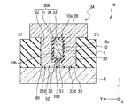
- FIG. 1 is a plan view showing a configuration example of a semiconductor device according to the first embodiment of the present disclosure.
- FIG. 2 is a cross-sectional view showing a configuration example of the semiconductor device according to the first embodiment of the present disclosure.
- FIG. 3 is a cross-sectional view showing a configuration example of the semiconductor device according to the first embodiment of the present disclosure.
- FIG. 4 is a cross-sectional view showing a configuration example of the semiconductor device according to the first embodiment of the present disclosure.
- FIG. 5 is a plan view showing the semiconductor device according to the first embodiment of the present disclosure, excluding the gate electrode.
- FIG. 6A is a cross-sectional view showing a method of manufacturing the semiconductor device according to the first embodiment of the present disclosure.
- FIG. 6A is a cross-sectional view showing a method of manufacturing the semiconductor device according to the first embodiment of the present disclosure.
- FIG. 6B is a cross-sectional view showing a method of manufacturing the semiconductor device according to the first embodiment of the present disclosure.
- FIG. 7A is a cross-sectional view showing a method of manufacturing the semiconductor device according to the first embodiment of the present disclosure.
- FIG. 7B is a cross-sectional view showing a method of manufacturing the semiconductor device according to the first embodiment of the present disclosure.
- FIG. 8A is a cross-sectional view showing a method of manufacturing the semiconductor device according to the first embodiment of the present disclosure.
- FIG. 8B is a cross-sectional view showing a method of manufacturing the semiconductor device according to the first embodiment of the present disclosure.
- FIG. 9A is a cross-sectional view showing a method of manufacturing the semiconductor device according to the first embodiment of the present disclosure.
- FIG. 9B is a cross-sectional view showing a method of manufacturing the semiconductor device according to the first embodiment of the present disclosure.
- FIG. 10A is a cross-sectional view showing a method of manufacturing the semiconductor device according to the first embodiment of the present disclosure.
- FIG. 10B is a cross-sectional view showing a method of manufacturing the semiconductor device according to the first embodiment of the present disclosure.
- FIG. 11A is a cross-sectional view showing a method of manufacturing the semiconductor device according to the first embodiment of the present disclosure.
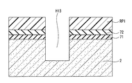
- FIG. 11B is a cross-sectional view showing a method of manufacturing the semiconductor device according to the first embodiment of the present disclosure.
- FIG. 12A is a cross-sectional view showing a method of manufacturing the semiconductor device according to the first embodiment of the present disclosure.
- FIG. 12B is a cross-sectional view showing a method of manufacturing the semiconductor device according to the first embodiment of the present disclosure.
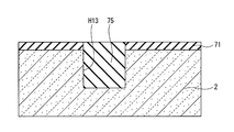
- FIG. 13A is a cross-sectional view showing a method of manufacturing the semiconductor device according to the first embodiment of the present disclosure.
- FIG. 13B is a cross-sectional view showing a method of manufacturing the semiconductor device according to the first embodiment of the present disclosure.
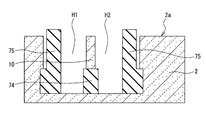
- FIG. 14A is a cross-sectional view showing a method of manufacturing the semiconductor device according to the first embodiment of the present disclosure.
- FIG. 14B is a cross-sectional view showing a method of manufacturing the semiconductor device according to the first embodiment of the present disclosure.
- FIG. 15A is a cross-sectional view showing a method of manufacturing the semiconductor device according to the first embodiment of the present disclosure.
- FIG. 15B is a cross-sectional view showing a method of manufacturing the semiconductor device according to the first embodiment of the present disclosure.
- FIG. 16A is a cross-sectional view showing a method of manufacturing a semiconductor device according to the first embodiment of the present disclosure.
- FIG. 16B is a cross-sectional view showing a method of manufacturing the semiconductor device according to the first embodiment of the present disclosure.
- FIG. 17 is a cross-sectional view showing a configuration example of the semiconductor device according to the second embodiment of the present disclosure.
- FIG. 18 is a cross-sectional view showing a configuration example of the semiconductor device according to the second embodiment of the present disclosure.
- FIG. 19A is a cross-sectional view showing a method of manufacturing a semiconductor device according to the second embodiment of the present disclosure.
- FIG. 19B is a cross-sectional view showing a method of manufacturing the semiconductor device according to the second embodiment of the present disclosure.
- FIG. 20A is a cross-sectional view showing a method of manufacturing the semiconductor device according to the second embodiment of the present disclosure.
- FIG. 20B is a cross-sectional view showing a method of manufacturing the semiconductor device according to the second embodiment of the present disclosure.
- FIG. 21A is a cross-sectional view showing a method of manufacturing the semiconductor device according to the second embodiment of the present disclosure.
- FIG. 21B is a cross-sectional view showing a method of manufacturing the semiconductor device according to the second embodiment of the present disclosure.
- FIG. 22 is a schematic view showing a configuration example of the image pickup apparatus according to the third embodiment of the present disclosure.
- FIG. 23 is a circuit diagram showing a configuration example of the pixel unit according to the third embodiment of the present disclosure.
- the direction may be explained using the words in the X-axis direction, the Y-axis direction, and the Z-axis direction.
- the X-axis direction and the Y-axis direction are directions parallel to the upper surface 10a of the semiconductor region 10.
- the X-axis direction and the Y-axis direction are also referred to as horizontal directions.
- the Z-axis direction is a direction that intersects the upper surface 10a of the semiconductor region 10 perpendicularly.
- the Z-axis direction is also called the depth direction.
- the X-axis direction, the Y-axis direction, and the Z-axis direction are orthogonal to each other.
- the X-axis direction is an example of the "second direction” of the present disclosure
- the Y-axis direction is an example of the "first direction” of the present disclosure
- the Z-axis direction is an example of the "third direction” of the present disclosure. Is.
- the first conductive type is the N type and the second conductive type is the P type will be exemplified.
- the conductive type may be selected in the opposite relationship, the first conductive type may be P type, and the second conductive type may be N type.
- FIG. 1 is a plan view showing a configuration example of the semiconductor device 1 according to the first embodiment of the present disclosure.
- 2 to 4 are cross-sectional views showing a configuration example of the semiconductor device 1 according to the first embodiment of the present disclosure.
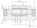
- FIG. 2 shows a cross section of the plan view shown in FIG. 1 cut along the line A1-A'1.
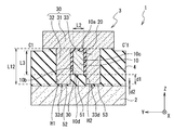
- FIG. 3 shows a cross section of the plan view shown in FIG. 1 cut along the B1-B'1 line.
- FIG. 4 shows a cross section of the plan view shown in FIG. 1 cut along the line C1-C'1.
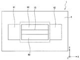
- FIG. 5 is a plan view showing the semiconductor device 1 according to the first embodiment of the present disclosure, excluding the gate electrode 30.
- the semiconductor device 1 includes a semiconductor substrate 2 and a first conductive type MOS (Metal Oxide Semiconductor) transistor 3 provided on the semiconductor substrate 2 (“Metal Oxide Semiconductor) Transistor 3 (““ An example of an electric field effect transistor) and an element separation layer 4 provided on the semiconductor substrate 2 are provided.
- MOS Metal Oxide Semiconductor
- the semiconductor substrate 2 is made of, for example, single crystal silicon.
- the semiconductor substrate 2 has a front surface 2a (an example of the "first main surface” of the present disclosure) and a back surface 2b located on the opposite side of the front surface 2a.
- a MOS transistor 3 is provided on the front surface 2a side of the semiconductor substrate 2.
- the element separation layer 4 is an insulating film for electrically separating adjacent elements in the horizontal direction, and is composed of, for example, a silicon oxide film (SiO 2 film).
- the MOS transistor 3 includes a second conductive type (for example, P type) semiconductor region 10 in which a channel is formed, a gate insulating film 20, a gate electrode 30, a source region 41 and a drain region provided on the semiconductor substrate 2.
- a 42, a first insulating film 51, a second insulating film 52, and a third insulating film 53 are provided.
- the semiconductor region 10 is, for example, a part of the semiconductor substrate 2 and is composed of single crystal silicon.
- the semiconductor region 10 is a portion formed by etching a part of the front surface 2a side of the semiconductor substrate 2.
- the shape of the semiconductor region 10 is, for example, a fin shape.
- the semiconductor region 10 has a shape that is long in the X-axis direction and short in the Y-axis direction.
- the length L1 of the semiconductor region 10 in the X-axis direction is 150 nm or more and 700 nm or less.
- the length (width) L2 of the semiconductor region 10 in the Y-axis direction is 15 nm or more and 1000 nm or less.
- the length (depth) L3 of the semiconductor region 10 in the Z-axis direction is 100 nm or more and 1000 nm or less.
- a trench H1 having a second insulating film 52 as a bottom surface is provided on one side of the semiconductor region 10, and a trench H2 having a third insulating film 53 as a bottom surface is provided on the other side of the semiconductor region 10. It is provided.
- the second portion 32 of the gate electrode 30 is arranged in the trench H1.
- a third portion 33 of the gate electrode 30 is arranged in the trench H2. The second part 32 and the third part 33 will be described later.
- the semiconductor region 10 is sandwiched from the Y-axis direction by the second portion 32 arranged in the trench H1 and the third portion 33 arranged in the trench H2.
- the gate insulating film 20 is provided so as to cover the upper surface 10a, the first side surface 10b, and the second side surface 10c of the semiconductor region 10.
- the first side surface 10b is located on one side of the upper surface 10a in the Y-axis direction.
- the second side surface 10c is located on the other side of the upper surface 10a in the Y-axis direction.
- the gate insulating film 20 is made of, for example, a SiO 2 film.
- the gate electrode 30 covers the semiconductor region 10 via the gate insulating film 20.
- the gate electrode 30 has a first portion 31 facing the upper surface 10a of the semiconductor region 10 via the gate insulating film 20, and a second portion 32 facing the first side surface 10b of the semiconductor region 10 via the gate insulating film 20.
- the semiconductor region 10 has a second side surface 10c and a third portion 33 facing the semiconductor region 10 via the gate insulating film 20.
- the second part 32 and the third part 33 are connected to the lower surface of the first part 31, respectively.
- the gate electrode 30 can simultaneously apply a gate voltage to the upper surface 10a, the first side surface 10b, and the second side surface 10c of the semiconductor region 10. That is, the gate electrode 30 can simultaneously apply the gate voltage to the semiconductor region 10 from a total of three directions, the upper side and the left and right sides. As a result, the gate electrode 30 can completely deplete the semiconductor region 10.
- the length L11 of the first portion 31 in the X-axis direction is, for example, 300 nm or more and 500 nm or less.
- the length L12 of the second portion 32 and the third portion 33 in the Z-axis direction is, for example, 120 nm or more and 1200 nm or less.
- the gate electrode 30 is made of, for example, a polysilicon (Poly-Si) film.
- the source region 41 is provided on the front surface 2a of the semiconductor substrate 2 and in the vicinity thereof. In the X-axis direction, the source region 41 is connected to one side of the semiconductor region 10.
- the drain region 42 is provided on the front surface 2a of the semiconductor substrate 2 and in the vicinity thereof. In the X-axis direction, the drain region 42 is connected to the other side of the semiconductor region 10.
- the source region 41 and the drain region 42 are first conductive type (for example, N type).
- the first insulating film 51 is arranged between the lower surface 10d of the semiconductor region 10 and the semiconductor substrate 2.
- the second insulating film 52 is arranged between the lower surface 32d of the second portion 32 of the gate electrode 30 and the semiconductor substrate 2.
- the third insulating film 53 is arranged between the lower surface 33d of the third portion 33 of the gate electrode 30 and the semiconductor substrate 2.
- the second insulating film 52 and the third insulating film 53 are thinner than the first insulating film 51.
- the thickness d1 of the first insulating film 51 is 10 nm or more and 800 nm or less.
- Each thickness d2 of the second insulating film 52 and the third insulating film 53 is 1 nm or more and 20 nm or less.
- the first insulating film 51, the second insulating film 52, and the third insulating film 53 are made of, for example, a SiO 2 film.
- the MOS transistor 3 may be referred to as a MOS transistor having a digging gate structure because the second portion 32 and the third portion 33 of the gate electrode 30 are arranged in the trenches H1 and H2. ..
- the MOS transistor 3 may be called a FinFET (FinFET: FinField Effect Transistor) because the semiconductor region 10 has a fin shape.
- the MOS transistor may be called a digging FinFET because of the above two shapes.
- the semiconductor device 1 uses various devices such as a film forming device (including a CVD (Chemical Vapor Deposition) device and a sputtering device), an ion implantation device, a heat treatment device, an etching device, and a CMP (Chemical Mechanical Polishing) device. Manufactured. Hereinafter, these devices are collectively referred to as manufacturing devices.
- a film forming device including a CVD (Chemical Vapor Deposition) device and a sputtering device
- an ion implantation device including a heat treatment device, an etching device, and a CMP (Chemical Mechanical Polishing) device.
- a CMP Chemical Mechanical Polishing
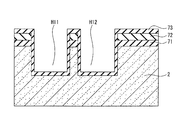
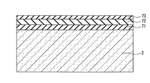
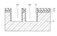
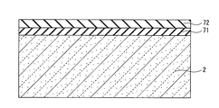
- 6A to 16B are cross-sectional views showing the manufacturing method of the semiconductor device 1 according to the first embodiment of the present disclosure in the order of processes.
- a in each figure shows a formation region of a MOS transistor 3 having a digging gate structure (hereinafter referred to as a digging region), and B in each figure is a formation region of a MOS transistor having a planar gate structure (hereinafter referred to as a digging region). , It is called a planar area.)
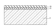
- the manufacturing apparatus uses a CVD method to form a silicon nitride film (SiN film) 71 on the front surface 2a of the semiconductor substrate 2.
- the manufacturing apparatus uses the CVD method to form the SiO 2 film 72 on the SiN film 71.
- the manufacturing apparatus partially removes the SiO 2 film 72, the SiN film 71, and the semiconductor substrate 2 in the dug region by using photolithography and etching techniques. As a result, the manufacturing apparatus forms trenches H11 and H12 in the digging region.
- the manufacturing apparatus uses a CVD method to form a SiN film 73 on the semiconductor substrate 2.
- the manufacturing apparatus partially removes the SiN film 73 using photolithography and anisotropic etching techniques. In the digging region, the SiN film 73 is removed from the bottom surfaces of the trenches H11 and H12 and the SiO 2 film 72. As a result, the semiconductor substrate 2 is exposed on the bottom surfaces of the trenches H11 and H12. Further, a SiN film 73 is left on the inner surface of the trenches H11 and H12. Further, in the planar region, the SiN film 73 is removed from the SiO 2 film 72.
- the manufacturing apparatus etches the bottom surfaces of the trenches H11 and H12 to dig down the trenches H11 and H12.
- the semiconductor substrate 2 is exposed not only on the bottom surfaces of the trenches H11 and H12, but also on the inner side surfaces of the lower portions of the trenches H11 and H12. Since Si remains in the lower part of Fin, this etching is performed by anisotropic etching.
- the manufacturing apparatus digs the trenches H11 and H12 perpendicularly to the horizontal direction (that is, in the depth direction) by anisotropic etching.
- the manufacturing apparatus thermally oxidizes the semiconductor substrate 2.
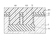
- the SiO 2 film 74 is formed in the lower part of the trenches H11 and H12.
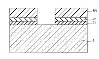
- the manufacturing apparatus forms the resist pattern RP1 in the digging region and the planar region.
- the resist pattern RP1 has a shape that opens a part of the planar region and covers the other region.
- the manufacturing apparatus uses the resist pattern RP1 as a mask to etch and remove the SiO 2 film 72 and the SiN film 71 in the planar region.
- the semiconductor substrate 2 is exposed from below the resist pattern RP1 in the planar region. Since the SiO 2 film 72 and the SiN film 71 in the dug region are covered with the resist pattern RP1, they remain without being etched. After that, the manufacturing apparatus removes the resist pattern RP1.
- the manufacturing apparatus etches the semiconductor substrate 2 exposed from under the SiO 2 film 72 in the planar region to form the trench H13 for element separation. After that, the manufacturing apparatus removes the resist pattern RP1. Next, the manufacturing apparatus uses a CVD method to form a SiO 2 film 75 (see FIGS. 13A and 13B described later) above the semiconductor substrate 2 and embed trenches H11, H12, and H13. Next, the manufacturing apparatus applies CMP treatment to the SiO 2 films 75 and 72 to expose the SiN film 71.
- the SiO 2 film 75 is left in the trenches H11, H12, and H13, and the SiO 2 film 75 is removed from the regions other than the trenches H11, H12, and H13.
- the SiO 2 film 75 left in the trench H13 functions as an element separation layer in the planar region.
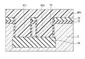
- the manufacturing apparatus forms a resist pattern RP2 in the digging region and the planar region.
- the resist pattern RP2 has a shape in which the trenches H11 and H12 and the region in the vicinity thereof are partially opened and the other regions are covered.
- the manufacturing apparatus uses the resist pattern RP2 as a mask to etch and remove the SiO 2 films 75 and 74 in the dug region.
- trenches H1 and H2 are formed in the dug region.
- the trench H1 is formed inside the trench H11 (see FIG. 13A), and the trench H2 is formed inside the trench H12 (see FIG. 13A).
- the manufacturing apparatus removes the resist pattern RP2.
- the SiO 2 film 75 left in the trenches H1 and H2 functions as an element separation layer 4 (see FIG. 1) in the digging region.
- the manufacturing apparatus wet-etches and removes the SiN films 71 and 73.
- the fin-shaped semiconductor region 10 is exposed in the dug region.
- the front surface 2a of the semiconductor substrate 2 is exposed in both the digging region and the planar region.
- the manufacturing apparatus thermally oxidizes the semiconductor substrate 2 including the semiconductor region 10.
- the manufacturing apparatus forms the gate insulating film 20 on the upper surface 10a, the first side surface 10b, and the second side surface 10c of the semiconductor region 10 in the digging region, and in the planar region.
- the gate insulating film 20 is formed on the front surface 2a of the semiconductor substrate 2.
- the manufacturing apparatus uses the CVD method to form a polysilicon film on the semiconductor substrate 2 and embed the trenches H1 and H2.
- the manufacturing apparatus forms the resist pattern RP3 on the polysilicon film.
- the resist pattern RP3 has a shape that covers the region where the gate electrode is formed and opens the other region.
- the manufacturing apparatus etches and removes the polysilicon film using the resist pattern RP3 as a mask.
- the manufacturing apparatus forms the gate electrode 30 in the digging region and the gate electrode 80 in the planar region.
- the manufacturing apparatus removes the resist pattern RP3.
- the manufacturing apparatus forms a source region and a drain region on the front surface 2a side of the semiconductor substrate 2 in both the digging region and the planar region.
- a semiconductor device 1 having a MOS transistor 3 having a digging gate structure and a MOS transistor having a planar gate structure on the same semiconductor substrate 2 is completed.
- the semiconductor device 1 includes a semiconductor substrate 2 and a MOS transistor 3 having a digging gate structure provided on the semiconductor substrate 2.
- the MOS transistor 3 includes a semiconductor region 10 in which a channel is formed, a gate electrode 30 covering the semiconductor region 10, a gate insulating film 20 arranged between the semiconductor region 10 and the gate electrode 30, the semiconductor region 10 and a semiconductor. It has a first insulating film 51 arranged between the substrate 2 and the substrate 2.
- the semiconductor region 10 has an upper surface 10a, a first side surface 10b, and a second side surface 10c.
- the first side surface 10b is located on one side of the upper surface 10a in the Y-axis direction parallel to the upper surface 10a.
- the second side surface 10c is located on the other side of the upper surface 10a in the Y-axis direction.
- the gate electrode 30 includes a first portion 31 facing the upper surface 10a of the semiconductor region 10 via the gate insulating film 20, a second portion 32 facing the first side surface 10b of the semiconductor region 10 via the gate insulating film 20, and a semiconductor. It has a second side surface 10c of the region 10 and a third portion 33 facing each other via the gate insulating film 20.
- the substrate bias effect can be reduced. Further, since the first insulating film 51 is arranged below the semiconductor region 10, it is possible to suppress the wraparound of the electric field from the drain region 42 to the source region 41 through the lower part of the semiconductor region 10. As a result, even when the source region 41 and the drain region 42 are formed deep in the depth direction (Z-axis direction) of the semiconductor substrate 2, it is possible to suppress the occurrence of the short-channel effect due to the wraparound of the electric field.
- the source region 41 and the drain region 42 can be formed deeply in the Z-axis direction and the substrate bias effect can be reduced, the mutual conductance (gm) of the MOS transistor 3 can be increased and the gain (gain) can be increased. It can be increased.
- As a method of reducing the substrate bias effect there is a method of using an SOI (Silicon on Insulator) substrate, but since the SOI substrate is expensive, the manufacturing cost of the semiconductor device increases. According to the first embodiment of the present disclosure, since it is not necessary to use the SOI substrate, it is possible to suppress the manufacturing cost and reduce the substrate bias effect at the same time.
- the gate electrode 30 can simultaneously apply a gate voltage to the semiconductor region 10 from a total of three directions on the upper side and both the left and right sides. As a result, the gate electrode 30 can easily completely deplete the semiconductor region 10, and the S value indicating the sub-threshold characteristic of the MOS transistor 3 can be reduced. High-speed switching operation of the MOS transistor 3 becomes possible.
- the second insulating film 52 and the third insulating film 53 are thinner than the first insulating film 51. That is, the lower surface 32d of the second portion 32 and the lower surface 33d of the third portion 33 are located closer to the semiconductor substrate 2 than the lower surface 10d of the semiconductor region 10.
- the length of the region in which the second portion 32 and the first side surface 10b of the semiconductor region 10 face each other and the length of the region in the Z-axis direction and the third portion 33 and the semiconductor region 33 It is possible to prevent variation in the length of the region facing the second side surface 10c of 10 in the Z-axis direction. As a result, it is possible to prevent variations in the gate width of the gate electrode 30.
- the gate electrode 30 faces the upper surface 10a of the semiconductor region 10 and the first side surface 10b and the second side surface 10c via the gate insulating film 20.
- the positional relationship between the semiconductor region 10 and the gate electrode 30 is not limited to this.
- the lower surface of the semiconductor region 10 that is, the surface closer to the semiconductor substrate 2 10d is also via the gate insulating film 20. It may be adjacent to the gate electrode 30.
- the gate width of the MOS transistor having a digging gate structure can be further expanded, and the complete depletion of the semiconductor region 10 can be made easier.
- FIGS. 17 and 18 are cross-sectional views showing a configuration example of the semiconductor device 1A according to the second embodiment of the present disclosure.
- FIG. 17 corresponds to a cross section obtained by cutting the plan view shown in FIG. 1 along the A1-A'1 line.
- FIG. 18 corresponds to a cross section obtained by cutting the plan view shown in FIG. 1 along the C1-C'1 line.
- the semiconductor device 1A according to the second embodiment includes a first conductive MOS transistor 3A (an example of the “field effect transistor” of the present disclosure) provided on the semiconductor substrate 2.
- the MOS transistor 3A according to the second embodiment is also a MOS transistor having a digging gate structure.
- the gate insulating film 20 and the gate electrode 30A are arranged between the lower surface 10d of the semiconductor region 10 and the semiconductor substrate 2.
- the gate electrode 30A has a first site 31, a second site 32, a third site 33, and a fourth site 34.
- the fourth portion 34 is adjacent to the lower surface 10d of the semiconductor region 10 via the gate insulating film 20.
- the gate electrode 30A can simultaneously apply a gate voltage to the upper surface 10a, the first side surface 10b, the second side surface 10c, and the lower surface 10d of the semiconductor region 10. That is, the gate electrode 30A can simultaneously apply a gate voltage to the semiconductor region 10 from a total of four directions, both upper and lower sides and both left and right sides.
- the manufacturing method of the semiconductor device 1A according to the second embodiment of the present disclosure will be described.
- the MOS transistor 3A having a digging gate structure shown in FIGS. 17 and 18 and the MOS transistor having a planar gate structure having a flat gate electrode are made of the same semiconductor substrate 2. The method of forming in parallel with the above will be described.
- FIGS. 19A to 21B are cross-sectional views showing the manufacturing method of the semiconductor device 1A according to the second embodiment of the present disclosure in the order of processes.
- a in each figure shows a digging area
- B in each figure shows a planar area.
- the steps up to the step of wet-etching and removing the SiN films 71 and 73 (see FIG. 14A) in the dug region to expose the fin-shaped semiconductor region 10 are the same as those in the first embodiment.
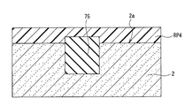
- the manufacturing apparatus forms a resist pattern RP4 in the digging region and the planar region.
- the resist pattern RP4 has a shape in which the trenches H11 and H12 and the region in the vicinity thereof are partially opened and the other regions are covered.
- the manufacturing apparatus uses the resist pattern RP4 as a mask to etch and remove the SiO 2 films 74 and 75 in the dug region.
- the manufacturing apparatus uses the resist pattern RP4 as a mask to etch and remove the SiO 2 films 74 and 75 in the dug region.
- trenches H1 and H2 and a cavity H3 are formed in the dug region.
- the cavity H3 is formed in a region including the lower part of the semiconductor region 10, and connects the trenches H1 and H2 to each other. Since the SiO 2 film 75 in the planar region is covered with the resist pattern RP4, it remains unetched. After that, the manufacturing apparatus removes the resist pattern RP4.
- the manufacturing apparatus thermally oxidizes the semiconductor substrate 2 including the semiconductor region 10.
- the manufacturing apparatus forms the gate insulating film 20 on the upper surface 10a, the first side surface 10b, the second side surface 10c, and the lower surface 10d of the semiconductor region 10 in the digging region, and the front surface of the semiconductor substrate 2 in the planar region.
- a gate insulating film 20 is formed on the surface 2a.
- the manufacturing apparatus uses a CVD method to form a polysilicon film on the semiconductor substrate 2 to embed trenches H1 and H2 and a cavity H3.
- the manufacturing apparatus forms the resist pattern RP5 on the polysilicon film.
- the resist pattern RP5 has a shape that covers the region where the gate electrode is formed and opens the other region.
- the manufacturing apparatus uses the resist pattern RP5 as a mask to etch and remove the polysilicon film.
- the gate electrode 30A is formed in the digging region, and the gate electrode 80 is formed in the planar region.
- the manufacturing apparatus removes the resist pattern RP5.
- the manufacturing apparatus forms a source region and a drain region on the front surface 2a side of the semiconductor substrate 2.
- a semiconductor device 1A having a MOS transistor 3A having a digging gate structure and a MOS transistor having a planar gate structure on the same semiconductor substrate 2 is completed.
- the semiconductor device 1A includes a semiconductor substrate 2 and a MOS transistor 3A having a digging gate structure provided on the semiconductor substrate 2.
- the MOS transistor 3A includes a semiconductor region 10 in which a channel is formed, a gate electrode 30A covering the semiconductor region 10, a gate insulating film 20 arranged between the semiconductor region 10 and the gate electrode 30A, a semiconductor region 10 and a semiconductor. It has a first insulating film 51 arranged between the substrate 2 and the substrate 2.
- the semiconductor region 10 has a lower surface 10d located on the opposite side of the upper surface 10a.
- the gate electrode 30A has a fourth portion 34 facing the lower surface 10d via the gate insulating film 20, in addition to the first portion 31, the second portion 32, and the third portion 33.
- the semiconductor device 1A has the same effect as the semiconductor device 1 according to the first embodiment. Further, the gate electrode 30A can simultaneously apply a gate voltage to the semiconductor region 10 from a total of four directions, both upper and lower sides and both left and right sides. As a result, the gate electrode 30A can more easily completely deplete the semiconductor region 10.
- the semiconductor device 1 according to the first embodiment or the semiconductor device 1A according to the second embodiment can be applied to an imaging device.
- an imaging device to which the semiconductor devices 1 and 1A are applied will be described.
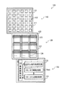
- FIG. 22 is a schematic view showing a configuration example of the image pickup apparatus 100 according to the third embodiment of the present disclosure.
- the image pickup apparatus 100 includes a first substrate portion 110, a second substrate portion 120, and a third substrate portion 130.
- the image pickup apparatus 100 is an image pickup apparatus having a three-dimensional structure, which is formed by laminating a first substrate portion 110, a second substrate portion 120, and a third substrate portion 130.
- the first substrate portion 110, the second substrate portion 120, and the third substrate portion 130 are laminated in this order.
- the first substrate unit 110 has a semiconductor substrate 111 and a plurality of sensor pixels 112 provided on the semiconductor substrate 111.
- the plurality of sensor pixels 112 perform photoelectric conversion.
- the plurality of sensor pixels 112 are provided in a matrix in the pixel region 113 of the first substrate portion 110.
- the second substrate portion 120 is provided on the semiconductor substrate 121, the readout circuit 122 provided on the semiconductor substrate 121, a plurality of pixel drive lines 123 provided on the semiconductor substrate 121 and extending in the row direction, and the semiconductor substrate 121. It has a plurality of vertical signal lines 124 extending in the row direction.
- the readout circuit 122 outputs a pixel signal based on the charge output from the sensor pixel 112.
- One readout circuit 122 is provided for every four sensor pixels 112.
- the third substrate unit 130 has a semiconductor substrate 131 and a logic circuit 132 provided on the semiconductor substrate 131.
- the logic circuit 132 has a function of processing a pixel signal, and includes, for example, a vertical drive circuit 133, a column signal processing circuit 134, a horizontal drive circuit 135, and a system control circuit 136.
- the vertical drive circuit 133 selects, for example, a plurality of sensor pixels 112 in order in line units.
- the column signal processing circuit 134 for example, performs a correlated double sampling (CDS) process on the pixel signal output from each sensor pixel 112 in the row selected by the vertical drive circuit 133.
- the column signal processing circuit 134 extracts the signal level of the pixel signal by performing CDS processing, for example, and holds pixel data according to the amount of light received by each sensor pixel 112.
- the system control circuit 136 controls the drive of each block (vertical drive circuit 133, column signal processing circuit 134, and horizontal drive circuit 135) in the logic circuit 132, for example.
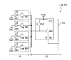
- FIG. 23 is a circuit diagram showing a configuration example of the pixel unit PU according to the third embodiment of the present disclosure.
- four sensor pixels 112 are electrically connected to one readout circuit 122 to form one pixel unit PU.
- the four sensor pixels 112 share one read circuit 122, and each output of the four sensor pixels 112 is input to the shared read circuit 122.
- Each sensor pixel 112 has a component common to each other.
- the identification numbers (1, 2, 3, FD) are added to the end of the code (for example, PD, TG, FD described later) of the component of each sensor pixel 112. 4) is given.
- the identification number at the end of the code of the component of each sensor pixel 112 is omitted.
- Each sensor pixel 112 is output from, for example, a photodiode PD (an example of the "light receiving element" of the present disclosure), a transfer transistor TR electrically connected to the photodiode PD, and a photodiode PD via the transfer transistor TR. It has a floating diffusion FD that temporarily holds the charged charge.
- the photodiode PD performs photoelectric conversion to generate an electric charge according to the amount of received light.
- the cathode of the photodiode PD is electrically connected to the source of the transfer transistor TR, and the anode of the photodiode PD is electrically connected to the reference potential line (eg, ground).
- the drain of the transfer transistor TR is electrically connected to the floating diffusion FD, and the gate electrode of the transfer transistor TR is electrically connected to the pixel drive line 123.
- the transfer transistor TR is, for example, a CMOS (Complementary Metal Oxide MOSFET) transistor.
- the floating diffusion FDs of the sensor pixels 112 sharing one read-out circuit 122 are electrically connected to each other and are also electrically connected to the input end of the common read-out circuit 122.
- the readout circuit 122 has, for example, an amplification transistor AMP, a reset transistor RST, and a selection transistor SEL.
- the selection transistor SEL may be omitted if necessary.
- the source of the reset transistor RST (the input end of the read circuit 122) is electrically connected to the floating diffusion FD, and the drain of the reset transistor RST is electrically connected to the power line VDD and the drain of the amplification transistor AMP.
- the gate electrode of the reset transistor RST is electrically connected to the pixel drive line 123 (see FIG. 22).
- the source of the amplification transistor AMP is electrically connected to the drain of the selection transistor SEL, and the gate electrode of the amplification transistor AMP is electrically connected to the source of the reset transistor RST.
- the source of the selection transistor SEL (the output end of the readout circuit 122) is electrically connected to the vertical signal line 124, and the gate electrode of the selection transistor SEL is electrically connected to the pixel drive line 123 (see FIG. 22). There is.
- the transfer transistor TR transfers the electric charge of the photodiode PD to the floating diffusion FD when the transfer transistor TR is turned on.
- the reset transistor RST resets the potential of the floating diffusion FD to a predetermined potential.
- the potential of the floating diffusion FD is reset to the potential of the power supply line VDD.
- the selection transistor SEL controls the output timing of the pixel signal from the read circuit 122.
- the amplification transistor AMP generates a voltage signal as a pixel signal according to the level of the electric charge held in the floating diffusion FD.
- the amplification transistor AMP constitutes a source follower type amplifier, and outputs a pixel signal having a voltage corresponding to the level of electric charge generated by the photodiode PD.
- the selection transistor SEL is turned on, the amplification transistor AMP amplifies the potential of the floating diffusion FD and outputs a voltage corresponding to the potential to the column signal processing circuit 134 via the vertical signal line 124.
- one or more of the reset transistor RST, the amplification transistor AMP, the transfer transistor TR, and the selection transistor SEL are the MOS transistor 3 described in the first embodiment or the MOS transistor 3A described in the second embodiment. Is used.
- the transfer transistor TR is provided on the first substrate portion 110.
- MOS transistors 3 and 3A having a digging gate structure may be used for the transfer transistor TR.
- the semiconductor substrate 111 corresponds to the semiconductor substrate 2 described in the first and second embodiments.
- a MOS transistor having a planar gate structure formed in parallel with the MOS transistors 3 and 3A is used for a pixel transistor other than the transfer transistor TR or a peripheral logic circuit arranged around the pixel region 113. Good.
- the reset transistor RST, the amplification transistor AMP, and the selection transistor SEL are provided on the second substrate portion 120.
- MOS transistors 3 and 3A having a digging gate structure may be used for one or more of the reset transistor RST, the amplification transistor AMP, and the selection transistor SEL.
- the semiconductor substrate 121 corresponds to the semiconductor substrate 2 described in the first and second embodiments.
- a planar gate structure formed in parallel with the MOS transistors 3 and 3A in a pixel transistor other than the reset transistor RST, the amplification transistor AMP and the selection transistor SEL, and a peripheral logic circuit arranged around the read circuit 122. MOS transistors may be used.
- the imaging device 100 includes a photodiode PD and a semiconductor device for transmitting an electric signal photoelectrically converted by the photodiode PD.
- the image pickup device 100 includes a semiconductor device 1 (or a semiconductor device 1A) with a reduced substrate bias effect as at least a part of the semiconductor device for electric signal transmission. As a result, the image pickup apparatus 100 can improve the performance such as reducing the noise of the image pickup data.
- the gate insulating film 20 a silicon oxynitride (SiON) film, a silicon nitride (Si 3 N 4) film can also be used. Further, as the gate insulating film 20, a composite film or the like in which several single-layer insulating films are laminated can also be used. A MOSFET in which an insulating film other than the SiO 2 film is used as the gate insulating film 20 may be referred to as a MISFET. MISFET means a more comprehensive field effect transistor, including MOSFETs.
- the present technology includes various embodiments not described here. At least one of the various omissions, substitutions and modifications of the components may be made without departing from the gist of the embodiments and modifications described above. Moreover, the effects described in the present specification are merely examples and are not limited, and other effects may be obtained.
- the present disclosure may also have the following structure.
- the field-effect transistor has a semiconductor region in which a channel is formed and A gate electrode covering the semiconductor region and A gate insulating film arranged between the semiconductor region and the gate electrode, It has a first insulating film arranged between the semiconductor region and the semiconductor substrate.
- the semiconductor region is It has an upper surface, a first side surface located on one side of the upper surface in a first direction parallel to the upper surface, and a second side surface located on the other side of the upper surface in the first direction.
- the gate electrode is A first portion facing the upper surface via the gate insulating film, A second portion facing the first side surface via the gate insulating film, A semiconductor device having the second side surface and a third portion facing the gate insulating film.
- the lower surface of the second portion and the lower surface of the third portion are located closer to the semiconductor substrate than the lower surface of the semiconductor region.
- (3) A second insulating film arranged between the semiconductor substrate and the second portion, A third insulating film arranged between the semiconductor substrate and the third portion is provided, and the second insulating film and the third insulating film are thinner than the first insulating film.
- the semiconductor region has a lower surface located on the opposite side of the upper surface.
- the semiconductor device according to any one of (1) to (3) above, wherein the gate electrode has a fourth portion facing the lower surface via the gate insulating film.
- a source region and a drain region provided on the semiconductor substrate are further provided. The source region is connected to one side of the semiconductor region in a second direction parallel to the top surface and orthogonal to the first direction.
- the semiconductor device according to any one of (1) to (4), wherein the drain region is connected to the other side of the semiconductor region in the second direction.
- the length of the gate electrode in the second direction is 300 nm or more and 500 nm or less.
- the semiconductor device according to (5) above.
- the length of the semiconductor region in the third direction orthogonal to the upper surface is 100 nm or more and 1000 nm or less.
- the semiconductor device according to any one of (1) to (6) above.
- Light receiving element and A semiconductor device for transmitting an electric signal photoelectrically converted by the light receiving element is provided.
- the semiconductor device is With a semiconductor substrate A field effect transistor provided on the semiconductor substrate is provided.
- the field effect transistor is The semiconductor region where the channel is formed and A gate electrode covering the semiconductor region and A gate insulating film arranged between the semiconductor region and the gate electrode, It has a first insulating film arranged between the semiconductor region and the semiconductor substrate.
- the semiconductor region is It has an upper surface, a first side surface located on one side of the upper surface in a first direction parallel to the upper surface, and a second side surface located on the other side of the upper surface in the first direction.
- the gate electrode is A first portion facing the upper surface via the gate insulating film, A second portion facing the first side surface via the gate insulating film, An image pickup apparatus having the second side surface and a third portion facing the gate insulating film.
Landscapes
- Engineering & Computer Science (AREA)
- Multimedia (AREA)
- Signal Processing (AREA)
- Insulated Gate Type Field-Effect Transistor (AREA)
- Solid State Image Pick-Up Elements (AREA)
- Transforming Light Signals Into Electric Signals (AREA)
- Thin Film Transistor (AREA)
- Electrodes Of Semiconductors (AREA)
Abstract
基板バイアス効果を低減することができる半導体装置と、この半導体装置を用いた撮像装置とを提供する。半導体装置は、半導体基板と、半導体基板の第1主面側に設けられた電界効果トランジスタと、を備える。電界効果トランジスタは、チャネルが形成される半導体領域と、半導体領域を覆うゲート電極と、半導体領域とゲート電極との間に配置されたゲート絶縁膜と、半導体領域と半導体基板との間に配置された第1絶縁膜と、を有する。半導体領域は、上面と、上面に平行な第1方向において上面の一方の側に位置する第1側面と、第1方向において上面の他方の側に位置する第2側面と、を有する。ゲート電極は、上面とゲート絶縁膜を介して向かい合う第1部位と、第1側面とゲート絶縁膜を介して向かい合う第2部位と、第2側面とゲート絶縁膜を介して向かい合う第3部位と、を有する。
Description
本開示は、半導体装置及び撮像装置に関する。
CMOS(Complementary Metal Oxide Semiconductor)イメージセンサに用いられる半導体装置として、垂直ゲート電極及びチャネルを有する非平面トランジスタが知られている(例えば、特許文献1参照)。
特許文献1に開示された非平面トランジスタのチャネル領域は、半導体基板と接しているため、基板バイアス効果を受ける。
本開示はこのような事情に鑑みてなされたもので、基板バイアス効果を低減することができる半導体装置と、この半導体装置を用いた撮像装置とを提供することを目的とする。
本開示の一態様に係る半導体装置は、半導体基板と、前記半導体基板の第1主面側に設けられた電界効果トランジスタと、を備え、前記電界効果トランジスタは、チャネルが形成される半導体領域と、前記半導体領域を覆うゲート電極と、前記半導体領域と前記ゲート電極との間に配置されたゲート絶縁膜と、前記半導体領域と前記半導体基板との間に配置された第1絶縁膜と、を有し、前記半導体領域は、上面と、前記上面に平行な第1方向において前記上面の一方の側に位置する第1側面と、前記第1方向において前記上面の他方の側に位置する第2側面と、を有し、前記ゲート電極は、前記上面と前記ゲート絶縁膜を介して向かい合う第1部位と、前記第1側面と前記ゲート絶縁膜を介して向かい合う第2部位と、前記第2側面と前記ゲート絶縁膜を介して向かい合う第3部位と、を有する。
これによれば、第1絶縁膜によって半導体領域と半導体基板との間が絶縁される。これにより、半導体装置は、基板バイアス効果を低減することができる。
本開示の一態様に係る撮像装置は、受光素子と、前記受光素子で光電変換された電気信号を伝送するための半導体装置と、を備え、前記半導体装置は、半導体基板と、前記半導体基板に設けられた電界効果トランジスタと、を備え、前記電界効果トランジスタは、チャネルが形成される半導体領域と、前記半導体領域を覆うゲート電極と、前記半導体領域と前記ゲート電極との間に配置されたゲート絶縁膜と、前記半導体領域と前記半導体基板との間に配置された第1絶縁膜と、を有し、前記半導体領域は、上面と、前記上面に平行な第1方向において前記上面の一方の側に位置する第1側面と、前記第1方向において前記上面の他方の側に位置する第2側面と、を有し、前記ゲート電極は、前記上面と前記ゲート絶縁膜を介して向かい合う第1部位と、前記第1側面と前記ゲート絶縁膜を介して向かい合う第2部位と、前記第2側面と前記ゲート絶縁膜を介して向かい合う第3部位と、を有する。
これによれば、撮像装置は、受光素子で光電変換された電気信号を伝送するための半導体装置として、基板バイアス効果を低減した半導体装置を用いることができる。これにより、撮像装置は性能の向上を図ることができる。
以下において、図面を参照して本開示の実施形態を説明する。以下の説明で参照する図面の記載において、同一又は類似の部分には同一又は類似の符号を付している。ただし、図面は模式的なものであり、厚みと平面寸法との関係、各層の厚みの比率等は現実のものとは異なることに留意すべきである。したがって、具体的な厚みや寸法は以下の説明を参酌して判断すべきものである。また、図面相互間においても互いの寸法の関係や比率が異なる部分が含まれていることは勿論である。
以下の説明における上下等の方向の定義は、単に説明の便宜上の定義であって、本開示の技術的思想を限定するものではない。例えば、対象を90°回転して観察すれば上下は左右に変換して読まれ、180°回転して観察すれば上下は反転して読まれることは勿論である。
以下の説明では、X軸方向、Y軸方向及びZ軸方向の文言を用いて、方向を説明する場合がある。例えば、X軸方向及びY軸方向は、半導体領域10の上面10aに平行な方向である。X軸方向及びY軸方向を水平方向ともいう。Z軸方向は、半導体領域10の上面10aと垂直に交わる方向である。Z軸方向を深さ方向ともいう。X軸方向、Y軸方向及びZ軸方向は、互いに直交する。なお、X軸方向は本開示の「第2方向」の一例であり、Y軸方向は本開示の「第1方向」の一例であり、Z軸方向は本開示の「第3方向」の一例である。
以下の説明では、第1導電型がN型、第2導電型がP型の場合について例示的に説明する。しかしながら、導電型を逆の関係に選択して、第1導電型をP型、第2導電型をN型としても構わない。
<実施形態1>
(半導体装置の構成例)
図1は、本開示の実施形態1に係る半導体装置1の構成例を示す平面図である。図2から図4は、本開示の実施形態1に係る半導体装置1の構成例を示す断面図である。図2は、図1に示す平面図をA1-A’1線で切断した断面を示している。図3は、図1に示す平面図をB1-B’1線で切断した断面を示している。図4は、図1に示す平面図をC1-C’1線で切断した断面を示している。図5は、本開示の実施形態1に係る半導体装置1において、ゲート電極30を除いて示した平面図である。
(半導体装置の構成例)
図1は、本開示の実施形態1に係る半導体装置1の構成例を示す平面図である。図2から図4は、本開示の実施形態1に係る半導体装置1の構成例を示す断面図である。図2は、図1に示す平面図をA1-A’1線で切断した断面を示している。図3は、図1に示す平面図をB1-B’1線で切断した断面を示している。図4は、図1に示す平面図をC1-C’1線で切断した断面を示している。図5は、本開示の実施形態1に係る半導体装置1において、ゲート電極30を除いて示した平面図である。
図1から図5に示すように、実施形態1に係る半導体装置1は、半導体基板2と、半導体基板2に設けられた第1導電型のMOS(Metal Oxide Semiconductor)トランジスタ3(本開示の「電界効果トランジスタ」の一例)と、半導体基板2に設けられた素子分離層4と、を備える。
半導体基板2は、例えば単結晶のシリコンで構成されている。半導体基板2は、おもて面2a(本開示の「第1主面」の一例)と、おもて面2aの反対側に位置するうら面2bと、を有する。半導体基板2のおもて面2a側に、MOSトランジスタ3が設けられている。素子分離層4は、水平方向で隣り合う素子同士を電気的に分離するための絶縁膜であり、例えば、シリコン酸化膜(SiO2膜)で構成されている。
MOSトランジスタ3は、チャネルが形成される第2導電型(例えば、P型)の半導体領域10と、ゲート絶縁膜20と、ゲート電極30と、半導体基板2に設けられたソース領域41及びドレイン領域42と、第1絶縁膜51と、第2絶縁膜52と、第3絶縁膜53と、を備える。
半導体領域10は、例えば半導体基板2の一部であり、単結晶のシリコンで構成されている。半導体領域10は、半導体基板2のおもて面2a側の一部をエッチングすることにより形成された部位である。半導体領域10の形状は、例えばフィン(Fin)形状である。
半導体領域10は、X軸方向に長く、Y軸方向に短い形状を有する。例えば、X軸方向における半導体領域10の長さL1は、150nm以上700nm以下である。Y軸方向における半導体領域10の長さ(幅)L2は、15nm以上1000nm以下である。Z軸方向における半導体領域10の長さ(深さ)L3は、100nm以上1000nm以下である。
Y軸方向において、半導体領域10の一方の側には第2絶縁膜52を底面とするトレンチH1が設けられ、半導体領域10の他方の側には第3絶縁膜53を底面とするトレンチH2が設けられている。トレンチH1には、ゲート電極30の第2部位32が配置されている。トレンチH2には、ゲート電極30の第3部位33が配置されている。第2部位32及び第3部位33については後で説明する。半導体領域10は、トレンチH1に配置された第2部位32と、トレンチH2に配置された第3部位33とによって、Y軸方向から挟まれている。
ゲート絶縁膜20は、半導体領域10の上面10aと、第1側面10bと、第2側面10cとを覆うように設けられている。第1側面10bは、Y軸方向において上面10aの一方の側に位置する。第2側面10cは、Y軸方向において上面10aの他方の側に位置する。ゲート絶縁膜20は、例えばSiO2膜で構成されている。
ゲート電極30は、ゲート絶縁膜20を介して半導体領域10を覆っている。例えば、ゲート電極30は、半導体領域10の上面10aとゲート絶縁膜20を介して向かい合う第1部位31と、半導体領域10の第1側面10bとゲート絶縁膜20を介して向かい合う第2部位32と、半導体領域10の第2側面10cとゲート絶縁膜20を介して向かい合う第3部位33と、を有する。第1部位31の下面に、第2部位32と第3部位33とがそれぞれ接続している。
これにより、ゲート電極30は、半導体領域10の上面10aと、第1側面10bと、第2側面10cとにゲート電圧を同時に印加することができる。つまり、ゲート電極30は、半導体領域10に対して、上側と左右両側の計3方向からゲート電圧を同時に印加することができる。これにより、ゲート電極30は、半導体領域10を完全空乏化することが可能となっている。
X軸方向における第1部位31の長さL11は、例えば300nm以上500nm以下である。Z軸方向における第2部位32及び第3部位33の各長さL12は、例えば120nm以上1200nm以下である。ゲート電極30は、例えばポリシリコン(Poly-Si)膜で構成されている。
ソース領域41は、半導体基板2のおもて面2aと、その近傍に設けられている。X軸方向において、ソース領域41は、半導体領域10の一方の側に接続している。ドレイン領域42は、半導体基板2のおもて面2aと、その近傍に設けられている。X軸方向において、ドレイン領域42は、半導体領域10の他方の側に接続している。ソース領域41及びドレイン領域42は、第1導電型(例えば、N型)である。
第1絶縁膜51は、半導体領域10の下面10dと半導体基板2との間に配置されている。第2絶縁膜52は、ゲート電極30の第2部位32の下面32dと半導体基板2との間に配置されている。第3絶縁膜53は、ゲート電極30の第3部位33の下面33dと半導体基板2との間に配置されている。第2絶縁膜52と第3絶縁膜53は、第1絶縁膜51よりも厚さが薄い。第1絶縁膜51の厚さd1は、10nm以上800nm以下である。第2絶縁膜52及び第3絶縁膜53の各厚さd2は、1nm以上20nm以下である。第1絶縁膜51、第2絶縁膜52及び第3絶縁膜53は、例えばSiO2膜で構成されている。
本開示の実施形態に係るMOSトランジスタ3は、トレンチH1、H2にゲート電極30の第2部位32と第3部位33とが配置されている形状から、掘り込みゲート構造のMOSトランジスタと呼んでもよい。または、MOSトランジスタ3は、半導体領域10がフィン形状を有することから、フィンフェット(FinFET:Fin Field Effect Transistor)と呼んでもよい。あるいは、MOSトランジスタは、上記2つの形状から、掘り込みFinFETと呼んでもよい。
(半導体装置の製造方法)
次に、本開示の実施形態1に係る半導体装置1の製造方法を説明する。この例では、半導体装置1の製造方法として、図1から図5に示した掘り込みゲート構造のMOSトランジスタ3と、ゲート電極が平坦であるプレーナゲート構造のMOSトランジスタとを、同一の半導体基板2に並行して形成する方法を説明する。
次に、本開示の実施形態1に係る半導体装置1の製造方法を説明する。この例では、半導体装置1の製造方法として、図1から図5に示した掘り込みゲート構造のMOSトランジスタ3と、ゲート電極が平坦であるプレーナゲート構造のMOSトランジスタとを、同一の半導体基板2に並行して形成する方法を説明する。
なお、半導体装置1は、成膜装置(CVD(Chemical Vapor Deposition)装置、スパッタ装置を含む)、イオン注入装置、熱処理装置、エッチング装置、CMP(Chemical Mechanical Polishing)装置など、各種の装置を用いて製造される。以下、これらの装置を、製造装置と総称する。
図6Aから図16Bは、本開示の実施形態1に係る半導体装置1の製造方法を工程順に示す断面図である。図6Aから図16Bにおいて、各図のAは掘り込みゲート構造のMOSトランジスタ3の形成領域(以下、掘り込み領域という)を示し、各図のBはプレーナゲート構造のMOSトランジスタの形成領域(以下、プレーナ領域という。)を示している。
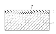
図6A及び図6Bにおいて、製造装置は、CVD法を用いて、半導体基板2のおもて面2a上にシリコン窒化膜(SiN膜)71を形成する。次に、製造装置は、CVD法を用いて、SiN膜71上にSiO2膜72を形成する。次に、製造装置は、フォトリソグラフィ及びエッチング技術を用いて、掘り込み領域のSiO2膜72、SiN膜71及び半導体基板2を部分的に除去する。これにより、製造装置は、掘り込み領域にトレンチH11、H12を形成する。
次に、図7A及び図7Bに示すように、製造装置は、CVD法を用いて、半導体基板2の上方にSiN膜73を形成する。次に、図8A及び図8Bに示すように、製造装置は、フォトリソグラフィ及び異方性エッチング技術を用いて、SiN膜73を部分的に除去する。掘り込み領域では、トレンチH11、H12の底面上とSiO2膜72上とからSiN膜73が除去される。これにより、トレンチH11、H12の底面において半導体基板2が露出する。また、トレンチH11、H12の内側面には、SiN膜73が残される。また、プレーナ領域では、SiO2膜72上からSiN膜73が除去される。
次に、図9A及び図9Bに示すように、製造装置は、トレンチH11、H12の底面をエッチングしてトレンチH11、H12を掘り下げる。これにより、トレンチH11、H12の底面だけでなく、トレンチH11、H12の下部の内側面においても半導体基板2が露出する。このエッチングは、Fin下部にSiを残すため、異方性エッチングで行う。製造装置は、異方性エッチングにより、トレンチH11、H12を水平方向に対して垂直(すなわち、深さ方向)に掘り下げる。
次に、製造装置は、半導体基板2を熱酸化する。これにより、図10A及び図10Bに示すように、トレンチH11、H12の下部にSiO2膜74が形成される。
次に、図11A及び図11Bに示すように、製造装置は、掘り込み領域とプレーナ領域とにレジストパターンRP1を形成する。レジストパターンRP1は、プレーナ領域の一部を開口し、それ以外の領域を覆う形状を有する。次に、製造装置は、レジストパターンRP1をマスクに用いて、プレーナ領域のSiO2膜72及びSiN膜71をエッチングして除去する。これにより、プレーナ領域において、レジストパターンRP1下から半導体基板2が露出する。掘り込み領域のSiO2膜72及びSiN膜71は、レジストパターンRP1覆われているため、エッチングされずに残る。その後、製造装置は、レジストパターンRP1を除去する。
次に、図12A及び図12Bに示すように、製造装置は、プレーナ領域において、SiO2膜72下から露出している半導体基板2をエッチングして、素子分離用のトレンチH13を形成する。その後、製造装置は、レジストパターンRP1を除去する。次に、製造装置は、CVD法を用いて、半導体基板2の上方にSiO2膜75(後述の図13A及び図13B参照)を形成して、トレンチH11、H12、H13を埋め込む。次に、製造装置は、SiO2膜75、72にCMP処理を施して、SiN膜71を露出させる。これにより、トレンチH11、H12、H13内にSiO2膜75が残され、トレンチH11、H12、H13以外の領域からSiO2膜75が除去される。トレンチH13内に残されたSiO2膜75は、プレーナ領域の素子分離層として機能する。
次に、図14A及び図14Bに示すように、製造装置は、掘り込み領域とプレーナ領域とにレジストパターンRP2を形成する。レジストパターンRP2は、トレンチH11、H12とその近傍の領域を部分的に開口し、それ以外の領域を覆う形状を有する。次に、製造装置は、レジストパターンRP2をマスクに用いて、掘り込み領域のSiO2膜75、74をエッチングして除去する。これにより、掘り込み領域にトレンチH1、H2が形成される。トレンチH1はトレンチH11(図13A参照)の内側に形成され、トレンチH2はトレンチH12(図13A参照)の内側に形成される。その後、製造装置は、レジストパターンRP2を除去する。なお、掘り込み領域において、トレンチH1、H2内に残されたSiO2膜75は、掘り込み領域の素子分離層4(図1参照)として機能する。
次に、製造装置は、SiN膜71、73をウェットエッチングして除去する。これにより、図15A及び図15Bに示すように、掘り込み領域においてフィン状の半導体領域10が露出する。また、掘り込み領域及びプレーナ領域の両方で、半導体基板2のおもて面2aが露出する。
次に、製造装置は、半導体領域10を含む半導体基板2を熱酸化する。これにより、図16A及び図16Bに示すように、製造装置は、掘り込み領域において半導体領域10の上面10a、第1側面10b及び第2側面10cにゲート絶縁膜20を形成するとともに、プレーナ領域において半導体基板2のおもて面2aにゲート絶縁膜20を形成する。
次に、製造装置は、CVD法を用いて、半導体基板2の上方にポリシリコン膜を形成して、トレンチH1、H2を埋め込む。次に、製造装置は、ポリシリコン膜上にレジストパターンRP3を形成する。レジストパターンRP3は、ゲート電極が形成される領域を覆い、それ以外の領域を開口する形状を有する。次に、製造装置は、レジストパターンRP3をマスクに用いて、ポリシリコン膜をエッチングして除去する。これにより、製造装置は、掘り込み領域にゲート電極30を形成し、プレーナ領域にゲート電極80を形成する。その後、製造装置は、レジストパターンRP3を除去する。次に、製造装置は、掘り込み領域及びプレーナ領域の両方において、半導体基板2のおもて面2a側にソース領域とドレイン領域とを形成する。
以上の工程を経て、掘り込みゲート構造のMOSトランジスタ3と、プレーナゲート構造のMOSトランジスタとを同一の半導体基板2に有する半導体装置1が完成する。
以上説明したように、本開示の実施形態1に係る半導体装置1は、半導体基板2と、半導体基板2に設けられた掘り込みゲート構造のMOSトランジスタ3と、を備える。MOSトランジスタ3は、チャネルが形成される半導体領域10と、半導体領域10を覆うゲート電極30と、半導体領域10とゲート電極30との間に配置されたゲート絶縁膜20と、半導体領域10と半導体基板2との間に配置された第1絶縁膜51と、を有する。半導体領域10は、上面10aと、第1側面10b及び第2側面10cを有する。第1側面10bは、上面10aに平行なY軸方向において上面10aの一方の側に位置する。第2側面10cは、Y軸方向において上面10aの他方の側に位置する。ゲート電極30は、半導体領域10の上面10aとゲート絶縁膜20を介して向かい合う第1部位31と、半導体領域10の第1側面10bとゲート絶縁膜20を介して向かい合う第2部位32と、半導体領域10の第2側面10cとゲート絶縁膜20を介して向かい合う第3部位33と、を有する。
これによれば、第1絶縁膜51によって半導体領域10と半導体基板2との間が絶縁されているため、基板バイアス効果を低減することができる。また、半導体領域10の下方に第1絶縁膜51が配置されているため、ドレイン領域42から半導体領域10の下方を通ってソース領域41に至る電界の回り込みを抑制することができる。これにより、ソース領域41とドレイン領域42とを半導体基板2の深さ方向(Z軸方向)に深く形成した場合でも、上記電界の回り込みによる短チャネル効果の発生を抑制することができる。
ソース領域41とドレイン領域42とをZ軸方向に深く形成することができ、また、基板バイアス効果を低減することができるので、MOSトランジスタ3の相互コンダクタンス(gm)の増大と利得(gain)の増大とが可能になる。なお、基板バイアス効果を低減する方法として、SOI(Silicon on Insulator)基板を用いる方法があるが、SOI基板は高価であるため半導体装置の製造コストが増大してしまう。本開示の実施形態1によれば、SOI基板を用いる必要がないため、製造コストの抑制と基板バイアス効果の低減とを両立することができる。
また、ゲート電極30は、半導体領域10に対して、上側と左右両側の計3方向からゲート電圧を同時に印加することができる。これにより、ゲート電極30は、半導体領域10を完全空乏化することが容易となり、MOSトランジスタ3のサブスレッシュホールド特性を示すS値の低減が可能になる。MOSトランジスタ3の高速スイッチング動作が可能になる。
また、第2絶縁膜52と第3絶縁膜53は、第1絶縁膜51よりも厚さが薄い。つまり、第2部位32の下面32d及び第3部位33の下面33dは、半導体領域10の下面10dよりも半導体基板2に近い側に位置する。これにより、トレンチH1、H2の深さにばらつきが生じる場合でも、第2部位32と半導体領域10の第1側面10bとが対向する領域のZ軸方向の長さと、第3部位33と半導体領域10の第2側面10cとが対向する領域のZ軸方向の長さとにばらつきが生じないようにすることができる。これにより、ゲート電極30のゲート幅にばらつきが生じることを抑制することができる。
<実施形態2>
本開示の実施形態1では、半導体領域10の上面10aと第1側面10b及び第2側面10cとにゲート絶縁膜20を介してゲート電極30が向かい合うことを説明した。しかしながら、本開示の実施形態において、半導体領域10とゲート電極30との位置関係はこれに限定されない。本開示の実施形態では、上面10a、第1側面10b及び第2側面10cに加えて、半導体領域10の下面(すなわち、半導体基板2に近い側の面)10dも、ゲート絶縁膜20を介してゲート電極30と隣り合っていてもよい。これにより、掘り込みゲート構造のMOSトランジスタのゲート幅をさらに拡大するとともに、半導体領域10の完全空乏化をより容易なものにすることができる。
本開示の実施形態1では、半導体領域10の上面10aと第1側面10b及び第2側面10cとにゲート絶縁膜20を介してゲート電極30が向かい合うことを説明した。しかしながら、本開示の実施形態において、半導体領域10とゲート電極30との位置関係はこれに限定されない。本開示の実施形態では、上面10a、第1側面10b及び第2側面10cに加えて、半導体領域10の下面(すなわち、半導体基板2に近い側の面)10dも、ゲート絶縁膜20を介してゲート電極30と隣り合っていてもよい。これにより、掘り込みゲート構造のMOSトランジスタのゲート幅をさらに拡大するとともに、半導体領域10の完全空乏化をより容易なものにすることができる。
図17及び図18は、本開示の実施形態2に係る半導体装置1Aの構成例を示す断面図である。図17は、図1に示した平面図をA1-A’1線で切断した断面に対応している。図18は、図1に示した平面図をC1-C’1線で切断した断面に対応している。図17及び図18に示すように、実施形態2に係る半導体装置1Aは、半導体基板2に設けられた第1導電型のMOSトランジスタ3A(本開示の「電界効果トランジスタ」の一例)を備える。
実施形態1に係るMOSトランジスタ3と同様に、実施形態2に係るMOSトランジスタ3Aも、掘り込みゲート構造のMOSトランジスタである。MOSトランジスタ3Aでは、半導体領域10の下面10dと半導体基板2との間に、ゲート絶縁膜20とゲート電極30Aとが配置されている。例えば、ゲート電極30Aは、第1部位31と、第2部位32と、第3部位33と、第4部位34とを有する。第4部位34は、半導体領域10の下面10dとゲート絶縁膜20を介して隣り合っている。
これにより、ゲート電極30Aは、半導体領域10の上面10aと、第1側面10bと、第2側面10cと、下面10dとにゲート電圧を同時に印加することができる。つまり、ゲート電極30Aは、半導体領域10に対して、上下両側と左右両側の計4方向からゲート電圧を同時に印加することができる。
次に、本開示の実施形態2に係る半導体装置1Aの製造方法を説明する。この例では、半導体装置1Aの製造方法として、図17及び図18に示した掘り込みゲート構造のMOSトランジスタ3Aと、ゲート電極が平坦であるプレーナゲート構造のMOSトランジスタとを、同一の半導体基板2に並行して形成する方法を説明する。
図19Aから図21Bは、本開示の実施形態2に係る半導体装置1Aの製造方法を工程順に示す断面図である。図19Aから図21Bにおいて、各図のAは掘り込み領域を示し、各図のBはプレーナ領域を示している。図19A及び図19Bにおいて、掘り込み領域のSiN膜71、73(図14A参照)をウェットエッチングして除去し、フィン状の半導体領域10を露出させる工程までは、実施形態1と同じである。実施形態2では、フィン状の半導体領域10が露出した後、製造装置は、掘り込み領域とプレーナ領域とにレジストパターンRP4を形成する。レジストパターンRP4は、トレンチH11、H12とその近傍の領域を部分的に開口し、それ以外の領域を覆う形状を有する。
次に、製造装置は、レジストパターンRP4をマスクに用いて、掘り込み領域のSiO2膜74、75をエッチングして除去する。これにより、図20A及び図20Bに示すように、掘り込み領域において、トレンチH1、H2と空洞部H3とが形成される。空洞部H3は、半導体領域10の下方を含む領域に形成されており、トレンチH1、H2同士を接続している。プレーナ領域のSiO2膜75は、レジストパターンRP4で覆われているのでエッチングされずに残る。その後、製造装置は、レジストパターンRP4を除去する。
次に、製造装置は、半導体領域10を含む半導体基板2を熱酸化する。これにより、製造装置は、掘り込み領域の半導体領域10の上面10a、第1側面10b、第2側面10c及び下面10dにゲート絶縁膜20を形成するとともに、プレーナ領域の半導体基板2のおもて面2aにゲート絶縁膜20を形成する。
次に、製造装置は、CVD法を用いて、半導体基板2の上方にポリシリコン膜を形成して、トレンチH1、H2と、空洞部H3を埋め込む。次に、図21A及び図21Bに示すように、製造装置は、ポリシリコン膜上にレジストパターンRP5を形成する。レジストパターンRP5は、ゲート電極が形成される領域を覆い、それ以外の領域を開口する形状を有する。次に、製造装置は、レジストパターンRP5をマスクに用いて、ポリシリコン膜をエッチングして除去する。これにより、掘り込み領域にゲート電極30Aが形成され、プレーナ領域にゲート電極80が形成される。その後、 製造装置は、レジストパターンRP5を除去する。その後、製造装置は、半導体基板2のおもて面2a側にソース領域とドレイン領域とを形成する。
以上の工程を経て、掘り込みゲート構造のMOSトランジスタ3Aと、プレーナゲート構造のMOSトランジスタとを同一の半導体基板2に有する半導体装置1Aが完成する。
以上説明したように、本開示の実施形態2に係る半導体装置1Aは、半導体基板2と、半導体基板2に設けられた掘り込みゲート構造のMOSトランジスタ3Aと、を備える。MOSトランジスタ3Aは、チャネルが形成される半導体領域10と、半導体領域10を覆うゲート電極30Aと、半導体領域10とゲート電極30Aとの間に配置されたゲート絶縁膜20と、半導体領域10と半導体基板2との間に配置された第1絶縁膜51と、を有する。半導体領域10は、上面10aの反対側に位置する下面10dを有する。ゲート電極30Aは、第1部位31、第2部位32及び第3部位33に加えて、下面10dとゲート絶縁膜20を介して向かい合う第4部位34を有する。
これによれば、半導体装置1Aは、実施形態1に係る半導体装置1と同様の効果を奏する。また、ゲート電極30Aは、半導体領域10に対して、上下両側と左右両側の計4方向からゲート電圧を同時に印加することができる。これにより、ゲート電極30Aは、半導体領域10をより容易に完全空乏化することが可能である。
<実施形態3>
実施形態1に係る半導体装置1又は実施形態2に係る半導体装置1Aは、撮像装置に適用可能である。以下、半導体装置1、1Aが適用される撮像装置の一例を説明する。
実施形態1に係る半導体装置1又は実施形態2に係る半導体装置1Aは、撮像装置に適用可能である。以下、半導体装置1、1Aが適用される撮像装置の一例を説明する。
図22は、本開示の実施形態3に係る撮像装置100の構成例を示す模式図である。撮像装置100は、第1基板部110と、第2基板部120と、第3基板部130とを備えている。撮像装置100は、第1基板部110と、第2基板部120と、第3基板部130とを貼り合わせて構成された3次元構造の撮像装置である。第1基板部110と、第2基板部120と、第3基板部130は、この順に積層されている。
第1基板部110は、半導体基板111と、半導体基板111に設けられた複数のセンサ画素112とを有する。複数のセンサ画素112は、光電変換を行う。複数のセンサ画素112は、第1基板部110における画素領域113内に行列状に設けられている。第2基板部120は、半導体基板121と、半導体基板121に設けられた読み出し回路122と、半導体基板121に設けられて行方向に延在する複数の画素駆動線123と、半導体基板121に設けられて列方向に延在する複数の垂直信号線124とを有する。読み出し回路122は、センサ画素112から出力された電荷に基づく画素信号を出力する。読み出し回路122は、4つのセンサ画素112ごとに1つずつ設けられている。
第3基板部130は、半導体基板131と、半導体基板131に設けられたロジック回路132を有する。ロジック回路132は、画素信号を処理する機能を有し、例えば、垂直駆動回路133、カラム信号処理回路134、水平駆動回路135およびシステム制御回路136を有する。
垂直駆動回路133は、例えば、複数のセンサ画素112を行単位で順に選択する。カラム信号処理回路134は、例えば、垂直駆動回路133によって選択された行の各センサ画素112から出力される画素信号に対して、相関二重サンプリング(Correlated Double Sampling:CDS)処理を施す。カラム信号処理回路134は、例えば、CDS処理を施すことにより、画素信号の信号レベルを抽出し、各センサ画素112の受光量に応じた画素データを保持する。水平駆動回路135は、例えば、カラム信号処理回路134に保持されている画素データを順次、外部に出力する。システム制御回路136は、例えば、ロジック回路132内の各ブロック(垂直駆動回路133、カラム信号処理回路134および水平駆動回路135)の駆動を制御する。
図23は、本開示の実施形態3に係る画素ユニットPUの構成例を示す回路図である。図23に示すように、撮像装置100では、4つのセンサ画素112が1つの読み出し回路122に電気的に接続されて、1つの画素ユニットPUを構成している。4つのセンサ画素112は、1つの読み出し回路122を共有しており、4つのセンサ画素112の各出力は共有する読み出し回路122に入力される。
各センサ画素112は、互いに共通の構成要素を有する。図23では、各センサ画素112の構成要素を互いに区別するために、各センサ画素112の構成要素の符号(例えば、後述のPD、TG、FD)の末尾に識別番号(1,2,3,4)が付与されている。以下では、各センサ画素112の構成要素を互いに区別する必要のない場合には、各センサ画素112の構成要素の符号の末尾の識別番号を省略するものとする。
各センサ画素112は、例えば、フォトダイオードPD(本開示の「受光素子」の一例)と、フォトダイオードPDと電気的に接続された転送トランジスタTRと、転送トランジスタTRを介してフォトダイオードPDから出力された電荷を一時的に保持するフローティングディフュージョンFDと、を有する。フォトダイオードPDは、光電変換を行って受光量に応じた電荷を発生する。フォトダイオードPDのカソードが転送トランジスタTRのソースに電気的に接続されており、フォトダイオードPDのアノードが基準電位線(例えばグラウンド)に電気的に接続されている。転送トランジスタTRのドレインがフローティングディフュージョンFDに電気的に接続され、転送トランジスタTRのゲート電極は画素駆動線123に電気的に接続されている。転送トランジスタTRは、例えば、CMOS(Complementary Metal Oxide Semiconductor)トランジスタである。
1つの読み出し回路122を共有する各センサ画素112のフローティングディフュージョンFDは、互いに電気的に接続されるとともに、共通の読み出し回路122の入力端に電気的に接続されている。読み出し回路122は、例えば、増幅トランジスタAMPと、リセットトランジスタRST及び選択トランジスタSELとを有する。なお、選択トランジスタSELは、必要に応じて省略してもよい。
リセットトランジスタRSTのソース(読み出し回路122の入力端)がフローティングディフュージョンFDに電気的に接続されており、リセットトランジスタRSTのドレインが電源線VDDおよび増幅トランジスタAMPのドレインに電気的に接続されている。リセットトランジスタRSTのゲート電極は画素駆動線123(図22参照)に電気的に接続されている。増幅トランジスタAMPのソースが選択トランジスタSELのドレインに電気的に接続されており、増幅トランジスタAMPのゲート電極がリセットトランジスタRSTのソースに電気的に接続されている。選択トランジスタSELのソース(読み出し回路122の出力端)が垂直信号線124に電気的に接続されており、選択トランジスタSELのゲート電極が画素駆動線123(図22参照)に電気的に接続されている。
転送トランジスタTRは、転送トランジスタTRがオン状態となると、フォトダイオードPDの電荷をフローティングディフュージョンFDに転送する。リセットトランジスタRSTは、フローティングディフュージョンFDの電位を所定の電位にリセットする。リセットトランジスタRSTがオン状態となると、フローティングディフュージョンFDの電位を電源線VDDの電位にリセットする。選択トランジスタSELは、読み出し回路122からの画素信号の出力タイミングを制御する。
増幅トランジスタAMPは、画素信号として、フローティングディフュージョンFDに保持された電荷のレベルに応じた電圧の信号を生成する。増幅トランジスタAMPは、ソースフォロア型のアンプを構成しており、フォトダイオードPDで発生した電荷のレベルに応じた電圧の画素信号を出力するものである。増幅トランジスタAMPは、選択トランジスタSELがオン状態となると、フローティングディフュージョンFDの電位を増幅して、その電位に応じた電圧を、垂直信号線124を介してカラム信号処理回路134に出力する。
本開示の実施形態3では、リセットトランジスタRST、増幅トランジスタAMP、転送トランジスタTR及び選択トランジスタSELのうちの1つ以上に、実施形態1で説明したMOSトランジスタ3又は実施形態2で説明したMOSトランジスタ3Aが用いられる。
例えば、図23に示すように、転送トランジスタTRは、第1基板部110に設けられている。転送トランジスタTRに、掘り込みゲート構造のMOSトランジスタ3、3Aが用いられてもよい。この場合、半導体基板111が実施形態1、2で説明した半導体基板2に相当する。また、転送トランジスタTR以外の他の画素トランジスタや、画素領域113の周辺に配置される周辺ロジック回路に、MOSトランジスタ3、3Aと並行して形成されたプレーナゲート構造のMOSトランジスタが用いられてもよい。
また、図23に示すように、リセットトランジスタRST、増幅トランジスタAMP及び選択トランジスタSELは、第2基板部120に設けられている。リセットトランジスタRST、増幅トランジスタAMP及び選択トランジスタSELのうちの1つ以上に、掘り込みゲート構造のMOSトランジスタ3、3Aが用いられてもよい。この場合、半導体基板121が実施形態1、2で説明した半導体基板2に相当する。また、リセットトランジスタRST、増幅トランジスタAMP及び選択トランジスタSEL以外の他の画素トランジスタや、読み出し回路122の周辺に配置される周辺ロジック回路に、MOSトランジスタ3、3Aと並行して形成されたプレーナゲート構造のMOSトランジスタが用いられてもよい。
以上説明したように、本開示の実施形態3に係る撮像装置100は、フォトダイオードPDと、フォトダイオードPDで光電変換された電気信号を伝送するための半導体装置とを備える。撮像装置100は、この電気信号伝送用の半導体装置の少なくとも一部として、基板バイアス効果を低減した半導体装置1(または、半導体装置1A)を備える。これにより、撮像装置100は、例えば撮像データの低ノイズ化など、性能の向上を図ることができる。
<その他の実施形態>
上記のように、本開示は実施形態及び変形例によって記載したが、この開示の一部をなす論述及び図面は本開示を限定するものであると理解すべきではない。この開示から当業者には様々な代替実施の形態、実施例及び運用技術が明らかとなろう。
上記のように、本開示は実施形態及び変形例によって記載したが、この開示の一部をなす論述及び図面は本開示を限定するものであると理解すべきではない。この開示から当業者には様々な代替実施の形態、実施例及び運用技術が明らかとなろう。
例えば、ゲート絶縁膜20には、シリコン酸窒化(SiON)膜、シリコン窒化物(Si3N4)膜も使用可能である。また、ゲート絶縁膜20には、単層の絶縁膜をいくつか積層した複合膜等も使用可能である。ゲート絶縁膜20としてSiO2膜以外の絶縁膜を用いたMOSFETは、MISFETと呼んでもよい。MISFETは、MOSFETを含む、より包括的な電界効果トランジスタを意味する。
このように、本技術はここでは記載していない様々な実施形態等を含むことは勿論である。上述した実施形態及び変形例の要旨を逸脱しない範囲で、構成要素の種々の省略、置換及び変更のうち少なくとも1つを行うことができる。また、本明細書に記載された効果はあくまでも例示であって限定されるものでは無く、また他の効果があってもよい。
なお、本開示は以下のような構成も取ることができる。
(1)半導体基板と、
前記半導体基板の第1主面側に設けられた電界効果トランジスタと、を備え、
前記電界効果トランジスタは、 チャネルが形成される半導体領域と、
前記半導体領域を覆うゲート電極と、
前記半導体領域と前記ゲート電極との間に配置されたゲート絶縁膜と、
前記半導体領域と前記半導体基板との間に配置された第1絶縁膜と、を有し、
前記半導体領域は、
上面と、前記上面に平行な第1方向において前記上面の一方の側に位置する第1側面と、前記第1方向において前記上面の他方の側に位置する第2側面と、を有し、
前記ゲート電極は、
前記上面と前記ゲート絶縁膜を介して向かい合う第1部位と、
前記第1側面と前記ゲート絶縁膜を介して向かい合う第2部位と、
前記第2側面と前記ゲート絶縁膜を介して向かい合う第3部位と、を有する半導体装置。
(2)前記第2部位の下面及び前記第3部位の下面は、前記半導体領域の下面よりも前記半導体基板に近い側に位置する、
前記(1)に記載の半導体装置。
(3)前記半導体基板と前記第2部位との間に配置された第2絶縁膜と、
前記半導体基板と前記第3部位との間に配置された第3絶縁膜と、を備え、前記第2絶縁膜と前記第3絶縁膜は、前記第1絶縁膜よりも厚さが薄い、
前記(1)又は(2)に記載の半導体装置。
(4)前記半導体領域は、前記上面の反対側に位置する下面を有し、
前記ゲート電極は、前記下面と前記ゲート絶縁膜を介して向かい合う第4部位を有する、前記(1)から(3)のいずれか1項に記載の半導体装置。
(5)前記半導体基板に設けられたソース領域及びドレイン領域、をさらに備え、
前記ソース領域は、前記上面に平行で前記第1方向と直交する第2方向において、前記半導体領域の一方の側に接続し、
前記ドレイン領域は、前記第2方向において前記半導体領域の他方の側に接続している、前記(1)から(4)のいずれか1項に記載の半導体装置。
(6)前記第2方向における前記ゲート電極の長さは、300nm以上500nm以下である、
前記(5)に記載の半導体装置。
(7)前記上面と直交する第3方向における前記半導体領域の長さは、100nm以上1000nm以下である、
前記(1)から(6)のいずれか1項に記載の半導体装置。
(8)受光素子と、
前記受光素子で光電変換された電気信号を伝送するための半導体装置と、を備え、
前記半導体装置は、
半導体基板と、
前記半導体基板に設けられた電界効果トランジスタと、を備え、
前記電界効果トランジスタは、
チャネルが形成される半導体領域と、
前記半導体領域を覆うゲート電極と、
前記半導体領域と前記ゲート電極との間に配置されたゲート絶縁膜と、
前記半導体領域と前記半導体基板との間に配置された第1絶縁膜と、を有し、
前記半導体領域は、
上面と、前記上面に平行な第1方向において前記上面の一方の側に位置する第1側面と、前記第1方向において前記上面の他方の側に位置する第2側面と、を有し、
前記ゲート電極は、
前記上面と前記ゲート絶縁膜を介して向かい合う第1部位と、
前記第1側面と前記ゲート絶縁膜を介して向かい合う第2部位と、
前記第2側面と前記ゲート絶縁膜を介して向かい合う第3部位と、を有する撮像装置。
(1)半導体基板と、
前記半導体基板の第1主面側に設けられた電界効果トランジスタと、を備え、
前記電界効果トランジスタは、 チャネルが形成される半導体領域と、
前記半導体領域を覆うゲート電極と、
前記半導体領域と前記ゲート電極との間に配置されたゲート絶縁膜と、
前記半導体領域と前記半導体基板との間に配置された第1絶縁膜と、を有し、
前記半導体領域は、
上面と、前記上面に平行な第1方向において前記上面の一方の側に位置する第1側面と、前記第1方向において前記上面の他方の側に位置する第2側面と、を有し、
前記ゲート電極は、
前記上面と前記ゲート絶縁膜を介して向かい合う第1部位と、
前記第1側面と前記ゲート絶縁膜を介して向かい合う第2部位と、
前記第2側面と前記ゲート絶縁膜を介して向かい合う第3部位と、を有する半導体装置。
(2)前記第2部位の下面及び前記第3部位の下面は、前記半導体領域の下面よりも前記半導体基板に近い側に位置する、
前記(1)に記載の半導体装置。
(3)前記半導体基板と前記第2部位との間に配置された第2絶縁膜と、
前記半導体基板と前記第3部位との間に配置された第3絶縁膜と、を備え、前記第2絶縁膜と前記第3絶縁膜は、前記第1絶縁膜よりも厚さが薄い、
前記(1)又は(2)に記載の半導体装置。
(4)前記半導体領域は、前記上面の反対側に位置する下面を有し、
前記ゲート電極は、前記下面と前記ゲート絶縁膜を介して向かい合う第4部位を有する、前記(1)から(3)のいずれか1項に記載の半導体装置。
(5)前記半導体基板に設けられたソース領域及びドレイン領域、をさらに備え、
前記ソース領域は、前記上面に平行で前記第1方向と直交する第2方向において、前記半導体領域の一方の側に接続し、
前記ドレイン領域は、前記第2方向において前記半導体領域の他方の側に接続している、前記(1)から(4)のいずれか1項に記載の半導体装置。
(6)前記第2方向における前記ゲート電極の長さは、300nm以上500nm以下である、
前記(5)に記載の半導体装置。
(7)前記上面と直交する第3方向における前記半導体領域の長さは、100nm以上1000nm以下である、
前記(1)から(6)のいずれか1項に記載の半導体装置。
(8)受光素子と、
前記受光素子で光電変換された電気信号を伝送するための半導体装置と、を備え、
前記半導体装置は、
半導体基板と、
前記半導体基板に設けられた電界効果トランジスタと、を備え、
前記電界効果トランジスタは、
チャネルが形成される半導体領域と、
前記半導体領域を覆うゲート電極と、
前記半導体領域と前記ゲート電極との間に配置されたゲート絶縁膜と、
前記半導体領域と前記半導体基板との間に配置された第1絶縁膜と、を有し、
前記半導体領域は、
上面と、前記上面に平行な第1方向において前記上面の一方の側に位置する第1側面と、前記第1方向において前記上面の他方の側に位置する第2側面と、を有し、
前記ゲート電極は、
前記上面と前記ゲート絶縁膜を介して向かい合う第1部位と、
前記第1側面と前記ゲート絶縁膜を介して向かい合う第2部位と、
前記第2側面と前記ゲート絶縁膜を介して向かい合う第3部位と、を有する撮像装置。
1、1A 半導体装置
2 半導体基板
2a おもて面
2b うら面
3、3A MOSトランジスタ
4 素子分離層
10 半導体領域
10a 上面
10b 第1側面
10c 第2側面
10d、32d、33d 下面
20 ゲート絶縁膜
30、30A ゲート電極
31 第1部位
32 第2部位
33 第3部位
34 第4部位
41 ソース領域
42 ドレイン領域
51 第1絶縁膜
52 第2絶縁膜
53 第3絶縁膜
71、73 SiN膜
73 SiN膜
74、75 SiO2膜
80 ゲート電極
100 撮像装置
110 第1基板部
111 半導体基板
112 センサ画素
113 画素領域
120 第2基板部
121 半導体基板
122 読み出し回路
123 画素駆動線
124 垂直信号線
130 第3基板部
131 半導体基板
132 ロジック回路
133 垂直駆動回路
134 カラム信号処理回路
135 水平駆動回路
136 システム制御回路
AMP 増幅トランジスタ
FD フローティングディフュージョン
H1、H2、H11、H12、H13 トレンチ
H2 トレンチ
PD フォトダイオードPU 画素ユニット
RP1、RP2、RP3、RP4、RP5 レジストパターン
RST リセットトランジスタ
SEL 選択トランジスタ
TR 転送トランジスタ
VDD 電源線
2 半導体基板
2a おもて面
2b うら面
3、3A MOSトランジスタ
4 素子分離層
10 半導体領域
10a 上面
10b 第1側面
10c 第2側面
10d、32d、33d 下面
20 ゲート絶縁膜
30、30A ゲート電極
31 第1部位
32 第2部位
33 第3部位
34 第4部位
41 ソース領域
42 ドレイン領域
51 第1絶縁膜
52 第2絶縁膜
53 第3絶縁膜
71、73 SiN膜
73 SiN膜
74、75 SiO2膜
80 ゲート電極
100 撮像装置
110 第1基板部
111 半導体基板
112 センサ画素
113 画素領域
120 第2基板部
121 半導体基板
122 読み出し回路
123 画素駆動線
124 垂直信号線
130 第3基板部
131 半導体基板
132 ロジック回路
133 垂直駆動回路
134 カラム信号処理回路
135 水平駆動回路
136 システム制御回路
AMP 増幅トランジスタ
FD フローティングディフュージョン
H1、H2、H11、H12、H13 トレンチ
H2 トレンチ
PD フォトダイオードPU 画素ユニット
RP1、RP2、RP3、RP4、RP5 レジストパターン
RST リセットトランジスタ
SEL 選択トランジスタ
TR 転送トランジスタ
VDD 電源線
Claims (8)
- 半導体基板と、
前記半導体基板の第1主面側に設けられた電界効果トランジスタと、を備え、
前記電界効果トランジスタは、
チャネルが形成される半導体領域と、
前記半導体領域を覆うゲート電極と、
前記半導体領域と前記ゲート電極との間に配置されたゲート絶縁膜と、
前記半導体領域と前記半導体基板との間に配置された第1絶縁膜と、を有し、
前記半導体領域は、
上面と、前記上面に平行な第1方向において前記上面の一方の側に位置する第1側面と、前記第1方向において前記上面の他方の側に位置する第2側面と、を有し、
前記ゲート電極は、
前記上面と前記ゲート絶縁膜を介して向かい合う第1部位と、
前記第1側面と前記ゲート絶縁膜を介して向かい合う第2部位と、
前記第2側面と前記ゲート絶縁膜を介して向かい合う第3部位と、を有する半導体装置。 - 前記第2部位の下面及び前記第3部位の下面は、前記半導体領域の下面よりも前記半導体基板に近い側に位置する、請求項1に記載の半導体装置。
- 前記半導体基板と前記第2部位との間に配置された第2絶縁膜と、
前記半導体基板と前記第3部位との間に配置された第3絶縁膜と、を備え、
前記第2絶縁膜と前記第3絶縁膜は、前記第1絶縁膜よりも厚さが薄い、請求項1に記載の半導体装置。 - 前記半導体領域は、前記上面の反対側に位置する下面を有し、
前記ゲート電極は、前記下面と前記ゲート絶縁膜を介して向かい合う第4部位を有する、請求項1に記載の半導体装置。 - 前記半導体基板に設けられたソース領域及びドレイン領域、をさらに備え、
前記ソース領域は、前記上面に平行で前記第1方向と直交する第2方向において、前記半導体領域の一方の側に接続し、
前記ドレイン領域は、前記第2方向において前記半導体領域の他方の側に接続している、請求項1に記載の半導体装置。 - 前記第2方向における前記ゲート電極の長さは、300nm以上500nm以下である、請求項5に記載の半導体装置。
- 前記上面と直交する第3方向における前記半導体領域の長さは、100nm以上1000nm以下である、請求項1に記載の半導体装置。
- 受光素子と、
前記受光素子で光電変換された電気信号を伝送するための半導体装置と、を備え、
前記半導体装置は、
半導体基板と、
前記半導体基板に設けられた電界効果トランジスタと、を備え、
前記電界効果トランジスタは、
チャネルが形成される半導体領域と、
前記半導体領域を覆うゲート電極と、 前記半導体領域と前記ゲート電極との間に配置されたゲート絶縁膜と、
前記半導体領域と前記半導体基板との間に配置された第1絶縁膜と、を有し、
前記半導体領域は、
上面と、前記上面に平行な第1方向において前記上面の一方の側に位置する第1側面と、前記第1方向において前記上面の他方の側に位置する第2側面と、を有し、
前記ゲート電極は、
前記上面と前記ゲート絶縁膜を介して向かい合う第1部位と、
前記第1側面と前記ゲート絶縁膜を介して向かい合う第2部位と、
前記第2側面と前記ゲート絶縁膜を介して向かい合う第3部位と、を有する撮像装置。
Priority Applications (1)
| Application Number | Priority Date | Filing Date | Title |
|---|---|---|---|
| US17/623,848 US20220367545A1 (en) | 2019-07-12 | 2020-05-26 | Semiconductor device and imaging device |
Applications Claiming Priority (2)
| Application Number | Priority Date | Filing Date | Title |
|---|---|---|---|
| JP2019-129745 | 2019-07-12 | ||
| JP2019129745A JP2021015891A (ja) | 2019-07-12 | 2019-07-12 | 半導体装置及び撮像装置 |
Publications (1)
| Publication Number | Publication Date |
|---|---|
| WO2021010024A1 true WO2021010024A1 (ja) | 2021-01-21 |
Family
ID=74210535
Family Applications (1)
| Application Number | Title | Priority Date | Filing Date |
|---|---|---|---|
| PCT/JP2020/020667 Ceased WO2021010024A1 (ja) | 2019-07-12 | 2020-05-26 | 半導体装置及び撮像装置 |
Country Status (3)
| Country | Link |
|---|---|
| US (1) | US20220367545A1 (ja) |
| JP (1) | JP2021015891A (ja) |
| WO (1) | WO2021010024A1 (ja) |
Cited By (2)
| Publication number | Priority date | Publication date | Assignee | Title |
|---|---|---|---|---|
| WO2022270039A1 (ja) * | 2021-06-24 | 2022-12-29 | ソニーセミコンダクタソリューションズ株式会社 | 固体撮像装置 |
| US12575210B2 (en) | 2022-07-08 | 2026-03-10 | Samsung Electronics Co., Ltd. | Image sensor |
Families Citing this family (4)
| Publication number | Priority date | Publication date | Assignee | Title |
|---|---|---|---|---|
| KR102886889B1 (ko) * | 2014-07-29 | 2025-11-18 | 인튜어티브 서지컬 오퍼레이션즈 인코포레이티드 | 환자 체벽 힘을 측정하기 위한 센서를 갖는 캐뉼러 |
| WO2022044797A1 (ja) * | 2020-08-24 | 2022-03-03 | ソニーセミコンダクタソリューションズ株式会社 | 半導体装置、撮像装置及び電子機器 |
| JP2023090324A (ja) * | 2021-12-17 | 2023-06-29 | ソニーセミコンダクタソリューションズ株式会社 | 半導体装置及び電子機器 |
| WO2026042556A1 (ja) * | 2024-08-21 | 2026-02-26 | ソニーセミコンダクタソリューションズ株式会社 | 光検出装置、および撮像装置、並びに電子機器 |
Citations (7)
| Publication number | Priority date | Publication date | Assignee | Title |
|---|---|---|---|---|
| JPH05198817A (ja) * | 1991-08-28 | 1993-08-06 | Sharp Corp | 半導体装置の構造および製造方法 |
| JP2006121093A (ja) * | 2004-10-20 | 2006-05-11 | Samsung Electronics Co Ltd | 非平面トランジスタを有する固体イメージセンサ素子及びその製造方法 |
| JP2007158139A (ja) * | 2005-12-07 | 2007-06-21 | Oki Electric Ind Co Ltd | 半導体装置およびその製造方法 |
| JP2012216776A (ja) * | 2011-03-31 | 2012-11-08 | Sony Corp | 半導体装置、および、その製造方法 |
| JP2014135353A (ja) * | 2013-01-09 | 2014-07-24 | National Institute Of Advanced Industrial & Technology | 半導体装置の製造方法 |
| JP2016502756A (ja) * | 2012-11-07 | 2016-01-28 | インターナショナル・ビジネス・マシーンズ・コーポレーションInternational Business Machines Corporation | 半導体構造および半導体構造を形成する方法 |
| US20170338322A1 (en) * | 2016-05-18 | 2017-11-23 | International Business Machines Corporation | Dummy dielectric fins for finfets with silicon and silicon germanium channels |
Family Cites Families (3)
| Publication number | Priority date | Publication date | Assignee | Title |
|---|---|---|---|---|
| JPH0214578A (ja) * | 1988-07-01 | 1990-01-18 | Fujitsu Ltd | 半導体装置 |
| US7456476B2 (en) * | 2003-06-27 | 2008-11-25 | Intel Corporation | Nonplanar semiconductor device with partially or fully wrapped around gate electrode and methods of fabrication |
| US9443900B2 (en) * | 2014-08-25 | 2016-09-13 | Taiwan Semiconductor Manufacturing Co., Ltd. | Pixel with multigate structure for charge storage or charge transfer |
-
2019
- 2019-07-12 JP JP2019129745A patent/JP2021015891A/ja active Pending
-
2020
- 2020-05-26 US US17/623,848 patent/US20220367545A1/en not_active Abandoned
- 2020-05-26 WO PCT/JP2020/020667 patent/WO2021010024A1/ja not_active Ceased
Patent Citations (7)
| Publication number | Priority date | Publication date | Assignee | Title |
|---|---|---|---|---|
| JPH05198817A (ja) * | 1991-08-28 | 1993-08-06 | Sharp Corp | 半導体装置の構造および製造方法 |
| JP2006121093A (ja) * | 2004-10-20 | 2006-05-11 | Samsung Electronics Co Ltd | 非平面トランジスタを有する固体イメージセンサ素子及びその製造方法 |
| JP2007158139A (ja) * | 2005-12-07 | 2007-06-21 | Oki Electric Ind Co Ltd | 半導体装置およびその製造方法 |
| JP2012216776A (ja) * | 2011-03-31 | 2012-11-08 | Sony Corp | 半導体装置、および、その製造方法 |
| JP2016502756A (ja) * | 2012-11-07 | 2016-01-28 | インターナショナル・ビジネス・マシーンズ・コーポレーションInternational Business Machines Corporation | 半導体構造および半導体構造を形成する方法 |
| JP2014135353A (ja) * | 2013-01-09 | 2014-07-24 | National Institute Of Advanced Industrial & Technology | 半導体装置の製造方法 |
| US20170338322A1 (en) * | 2016-05-18 | 2017-11-23 | International Business Machines Corporation | Dummy dielectric fins for finfets with silicon and silicon germanium channels |
Cited By (3)
| Publication number | Priority date | Publication date | Assignee | Title |
|---|---|---|---|---|
| WO2022270039A1 (ja) * | 2021-06-24 | 2022-12-29 | ソニーセミコンダクタソリューションズ株式会社 | 固体撮像装置 |
| US12453195B2 (en) | 2021-06-24 | 2025-10-21 | Sony Semiconductor Solutions Corporation | Solid-state imaging device |
| US12575210B2 (en) | 2022-07-08 | 2026-03-10 | Samsung Electronics Co., Ltd. | Image sensor |
Also Published As
| Publication number | Publication date |
|---|---|
| JP2021015891A (ja) | 2021-02-12 |
| US20220367545A1 (en) | 2022-11-17 |
Similar Documents
| Publication | Publication Date | Title |
|---|---|---|
| WO2021010024A1 (ja) | 半導体装置及び撮像装置 | |
| JP6083930B2 (ja) | 光電変換装置および撮像システム、光電変換装置の製造方法 | |
| US12068349B2 (en) | Method of manufacturing solid-state image sensor, solid-state image sensor, and camera | |
| WO2021084959A1 (ja) | 撮像装置及び電子機器 | |
| JP2015109343A (ja) | 半導体装置の製造方法 | |
| WO2020218503A1 (ja) | 撮像装置 | |
| WO2012120653A1 (ja) | 半導体装置の製造方法、及び、半導体装置 | |
| KR102905037B1 (ko) | 반도체 장치 및 반도체 장치의 제조 방법, 촬상 장치 | |
| JP6346488B2 (ja) | 半導体装置、固体撮像装置、それらの製造方法およびカメラ | |
| US10777596B2 (en) | Imaging apparatus, method of manufacturing the same, and device | |
| US20230246043A1 (en) | Semiconductor device and imaging apparatus | |
| US9887220B2 (en) | Method for manufacturing imaging apparatus, and imaging apparatus | |
| KR100775688B1 (ko) | 반도체 장치의 제조 방법 | |
| WO2023090206A1 (ja) | 撮像装置及び半導体装置 | |
| JP6362121B2 (ja) | 光電変換装置および撮像システム、光電変換装置の製造方法 | |
| US20250048758A1 (en) | Semiconductor device, method of manufacturing semiconductor device, and imaging device | |
| WO2023248648A1 (ja) | 半導体装置及び電子機器 | |
| JP2019161216A (ja) | 撮像装置およびその製造方法ならびに機器 | |
| JP2009152486A (ja) | 半導体装置の製造方法及び半導体装置 |
Legal Events
| Date | Code | Title | Description |
|---|---|---|---|
| 121 | Ep: the epo has been informed by wipo that ep was designated in this application |
Ref document number: 20840245 Country of ref document: EP Kind code of ref document: A1 |
|
| NENP | Non-entry into the national phase |
Ref country code: DE |
|
| 122 | Ep: pct application non-entry in european phase |
Ref document number: 20840245 Country of ref document: EP Kind code of ref document: A1 |