WO2020256409A1 - 자기장 차폐시트 및 이의 제조방법 - Google Patents
자기장 차폐시트 및 이의 제조방법 Download PDFInfo
- Publication number
- WO2020256409A1 WO2020256409A1 PCT/KR2020/007848 KR2020007848W WO2020256409A1 WO 2020256409 A1 WO2020256409 A1 WO 2020256409A1 KR 2020007848 W KR2020007848 W KR 2020007848W WO 2020256409 A1 WO2020256409 A1 WO 2020256409A1
- Authority
- WO
- WIPO (PCT)
- Prior art keywords
- sheet
- sheet body
- magnetic field
- area
- field shielding
- Prior art date
Links
- 238000004519 manufacturing process Methods 0.000 title claims description 24
- 229910045601 alloy Inorganic materials 0.000 claims abstract description 13
- 239000000956 alloy Substances 0.000 claims abstract description 13
- 229910000808 amorphous metal alloy Inorganic materials 0.000 claims abstract description 13
- 238000004080 punching Methods 0.000 claims description 90
- 238000000034 method Methods 0.000 claims description 48
- 239000012790 adhesive layer Substances 0.000 claims description 31
- 230000001681 protective effect Effects 0.000 claims description 23
- 239000000853 adhesive Substances 0.000 claims description 5
- 230000001070 adhesive effect Effects 0.000 claims description 5
- 239000010410 layer Substances 0.000 claims description 5
- 230000000149 penetrating effect Effects 0.000 claims description 5
- 239000000758 substrate Substances 0.000 claims description 4
- 230000008569 process Effects 0.000 description 27
- 230000035515 penetration Effects 0.000 description 13
- 239000012467 final product Substances 0.000 description 11
- 230000035699 permeability Effects 0.000 description 9
- 238000010586 diagram Methods 0.000 description 6
- 230000005540 biological transmission Effects 0.000 description 5
- 239000002184 metal Substances 0.000 description 5
- 239000002159 nanocrystal Substances 0.000 description 5
- 230000000694 effects Effects 0.000 description 4
- 230000004907 flux Effects 0.000 description 4
- 238000004891 communication Methods 0.000 description 3
- 239000000463 material Substances 0.000 description 3
- 238000003825 pressing Methods 0.000 description 3
- 230000002542 deteriorative effect Effects 0.000 description 2
- 239000000696 magnetic material Substances 0.000 description 2
- 230000009467 reduction Effects 0.000 description 2
- 230000008901 benefit Effects 0.000 description 1
- 230000009351 contact transmission Effects 0.000 description 1
- 238000005520 cutting process Methods 0.000 description 1
- 230000007423 decrease Effects 0.000 description 1
- 230000006866 deterioration Effects 0.000 description 1
- 238000010438 heat treatment Methods 0.000 description 1
- 239000007788 liquid Substances 0.000 description 1
- 229920000642 polymer Polymers 0.000 description 1
- 238000000926 separation method Methods 0.000 description 1
- 229910000859 α-Fe Inorganic materials 0.000 description 1
Images


Classifications
-
- H—ELECTRICITY
- H04—ELECTRIC COMMUNICATION TECHNIQUE
- H04B—TRANSMISSION
- H04B5/00—Near-field transmission systems, e.g. inductive or capacitive transmission systems
- H04B5/70—Near-field transmission systems, e.g. inductive or capacitive transmission systems specially adapted for specific purposes
- H04B5/79—Near-field transmission systems, e.g. inductive or capacitive transmission systems specially adapted for specific purposes for data transfer in combination with power transfer
-
- H—ELECTRICITY
- H02—GENERATION; CONVERSION OR DISTRIBUTION OF ELECTRIC POWER
- H02J—CIRCUIT ARRANGEMENTS OR SYSTEMS FOR SUPPLYING OR DISTRIBUTING ELECTRIC POWER; SYSTEMS FOR STORING ELECTRIC ENERGY
- H02J50/00—Circuit arrangements or systems for wireless supply or distribution of electric power
- H02J50/70—Circuit arrangements or systems for wireless supply or distribution of electric power involving the reduction of electric, magnetic or electromagnetic leakage fields
-
- H—ELECTRICITY
- H01—ELECTRIC ELEMENTS
- H01F—MAGNETS; INDUCTANCES; TRANSFORMERS; SELECTION OF MATERIALS FOR THEIR MAGNETIC PROPERTIES
- H01F27/00—Details of transformers or inductances, in general
- H01F27/34—Special means for preventing or reducing unwanted electric or magnetic effects, e.g. no-load losses, reactive currents, harmonics, oscillations, leakage fields
- H01F27/36—Electric or magnetic shields or screens
-
- H—ELECTRICITY
- H01—ELECTRIC ELEMENTS
- H01F—MAGNETS; INDUCTANCES; TRANSFORMERS; SELECTION OF MATERIALS FOR THEIR MAGNETIC PROPERTIES
- H01F41/00—Apparatus or processes specially adapted for manufacturing or assembling magnets, inductances or transformers; Apparatus or processes specially adapted for manufacturing materials characterised by their magnetic properties
- H01F41/02—Apparatus or processes specially adapted for manufacturing or assembling magnets, inductances or transformers; Apparatus or processes specially adapted for manufacturing materials characterised by their magnetic properties for manufacturing cores, coils, or magnets
- H01F41/0206—Manufacturing of magnetic cores by mechanical means
-
- H—ELECTRICITY
- H01—ELECTRIC ELEMENTS
- H01Q—ANTENNAS, i.e. RADIO AERIALS
- H01Q1/00—Details of, or arrangements associated with, antennas
- H01Q1/52—Means for reducing coupling between antennas; Means for reducing coupling between an antenna and another structure
- H01Q1/526—Electromagnetic shields
-
- H—ELECTRICITY
- H02—GENERATION; CONVERSION OR DISTRIBUTION OF ELECTRIC POWER
- H02J—CIRCUIT ARRANGEMENTS OR SYSTEMS FOR SUPPLYING OR DISTRIBUTING ELECTRIC POWER; SYSTEMS FOR STORING ELECTRIC ENERGY
- H02J50/00—Circuit arrangements or systems for wireless supply or distribution of electric power
- H02J50/20—Circuit arrangements or systems for wireless supply or distribution of electric power using microwaves or radio frequency waves
-
- H—ELECTRICITY
- H05—ELECTRIC TECHNIQUES NOT OTHERWISE PROVIDED FOR
- H05K—PRINTED CIRCUITS; CASINGS OR CONSTRUCTIONAL DETAILS OF ELECTRIC APPARATUS; MANUFACTURE OF ASSEMBLAGES OF ELECTRICAL COMPONENTS
- H05K9/00—Screening of apparatus or components against electric or magnetic fields
- H05K9/0073—Shielding materials
- H05K9/0075—Magnetic shielding materials
Definitions
- the present invention relates to a magnetic field shielding sheet and a method of manufacturing the same.
- NFC Near field communication
- wireless charging are essentially contactless transmission methods.
- Such a non-contact transmission method is implemented through an antenna that transmits or receives a magnetic field, and a magnetic field shielding sheet disposed on one side of the antenna so as to smoothly transmit or receive the magnetic field.
- a sheet made of a magnetic material such as an amorphous ribbon sheet, a ferrite sheet, or a polymer sheet is used as the magnetic field shielding sheet.
- the magnetic field shielding sheet is a sheet in a form separated into a plurality of pieces so as to greatly reduce loss due to eddy current or improve the flexibility of the sheet itself.
- the magnetic field shielding sheet may be separated into a plurality of pieces through a flake process.
- a flake process may be performed through a metal roller and a rubber roller in which a plurality of uneven or spherical balls are formed on the outer surface.
- the magnetic field shielding sheet when the magnetic field shielding sheet is passed through the metal roller and the rubber roller multiple times in a state in which the metal roller and the rubber roller are disposed oppositely, the magnetic field shielding sheet may be separated into a plurality of pieces.
- the entire area of the sheet is pressed through the pair of rollers. Accordingly, in the magnetic field shielding sheet produced through the flake process, the entire sheet is inevitably separated into a plurality of pieces.
- a magnetic field shielding sheet separated into a plurality of pieces through a conventional flake process may have uniform characteristics only when the flake process is performed a plurality of times.
- the present invention was devised in consideration of the above points, and a magnetic field shielding sheet capable of realizing a high permeability of 2000 or more while having a very thin thickness by forming a penetration part locally and cracks caused by it in only a part of the total area And there is an object to provide a method for manufacturing the same.
- another object of the present invention is to provide a method of manufacturing a magnetic field shielding sheet capable of selectively forming cracks in a region corresponding to an antenna among the total area even if a separate flake process is not performed.
- the present invention is a magnetic field shielding sheet for an antenna including a hollow portion having a predetermined area in a central portion and a pattern portion surrounding the hollow portion, comprising at least one of an amorphous alloy and a nanocrystalline alloy A sheet body formed of a ribbon sheet; A plurality of through portions formed in a region of the sheet body corresponding to the pattern portion; It provides a magnetic field shielding sheet including; and a plurality of cracks extending from the through portion.
- the through portion may be formed to be longer than the width.
- the plurality of through portions may be spaced apart from each other.
- the through portion may include a first portion formed in a region corresponding to the pattern portion and a second portion extending from the first portion to a region corresponding to the hollow portion of the antenna.
- the plurality of through portions may be connected to each other through the second portion.
- the plurality of through portions may be formed such that each second portion is connected to each other at a central point of the antenna hollow portion.
- the sheet body may be a multilayer sheet in which at least two or more layers of the plurality of ribbon sheets are stacked, and the sheet body may include a protective film attached to at least one of an upper surface and a lower surface through an adhesive layer. have.
- the magnetic field shielding sheet may have a total thickness of 55 ⁇ m to 85 ⁇ m.
- the plurality of through portions a first through portion formed in a direction perpendicular to the width direction or the length direction of the sheet body; A second through portion formed in a direction parallel to the width direction or the length direction of the sheet body; A third through part formed to be inclined at a predetermined angle with respect to the width direction or the length direction of the sheet body; And a fourth through part formed in an arc shape having a predetermined curvature. At least one or more of them may be included.
- the present invention is a magnetic field shielding sheet for an antenna comprising a hollow portion having a predetermined area in the central portion and a pattern portion surrounding the hollow portion, a ribbon sheet comprising at least one of an amorphous alloy and a nanocrystalline alloy is an adhesive layer
- a sheet body formed of a multilayered sheet stacked in two to three layers as a medium;
- a plurality of through portions formed through the sheet body in an arrangement area corresponding to the pattern portion and formed in a linear shape having a length longer than a width;
- a plurality of cracks extending from the through part toward the sheet body, wherein each of the plurality of through parts is formed in a linear shape having a width of 0.1 mm to 0.4 mm, and the plurality of through parts has a total number of 4 It provides a magnetic field shielding sheet formed so as not to be connected to each other and is 16.
- the present invention is a magnetic field shielding sheet for an antenna including a hollow portion having a predetermined area in the central portion and a pattern portion surrounding the hollow portion, formed of a ribbon sheet containing at least one of an amorphous alloy and a nanocrystalline alloy Seat body; A plurality of through portions formed in a corresponding region of the sheet body corresponding to the hollow portion of the antenna; It provides a magnetic field shielding sheet including; and a plurality of cracks extending from the through portion.
- the plurality of through portions may be arranged to surround the center point of the corresponding area, and a partial area including the center point of the corresponding area among the corresponding areas is formed through a plurality of cracks extending from the plurality of through portions. It may be formed separately into a plurality of pieces.
- the present invention is a wireless power reception antenna comprising a hollow portion having a predetermined area in the central portion and a pattern portion surrounding the hollow portion; And the above-described magnetic field shielding sheet disposed on one surface of the antenna for receiving wireless power.
- the above-described wireless power reception module can be applied to a portable terminal device.
- the present invention is a method of manufacturing a magnetic field shielding sheet for an antenna comprising a hollow portion having a predetermined area in the central portion and a pattern portion surrounding the hollow portion, comprising at least one of a heat-treated amorphous alloy and a nanocrystalline alloy
- a sheet body having a first area formed of a ribbon sheet First punching the sheet body to form a plurality of cracks extending from the through portion while forming a through portion having a predetermined width and length in an inner region of the sheet body; And secondary punching of the sheet body to form a shielding sheet having a second area that is relatively narrower than the first area while including the through part.
- the through part may be formed through the arrangement area in which the pattern part of the antenna is disposed.
- the through portion may be formed through the corresponding region corresponding to the hollow portion of the antenna.
- the step of first punching the sheet body may include a ring-shaped rim blade for forming an rim of the penetrating part and the rim blade so that the cut piece cut from the sheet body can be pressed and separated through the rim blade. It can be performed through a mold including a separating member formed in the inner region of the.
- the second punching of the sheet body may be a step of forming an outer border defining the second area on the sheet body so that the shielding sheet can be separated from the sheet body.
- the step of preparing the sheet body may include forming a multilayer sheet in which a plurality of ribbon sheets are stacked in multiple layers via a first adhesive layer; And attaching a protective film to a lower surface of the multilayer sheet via a second adhesive layer coated with an adhesive on both sides of the substrate, wherein the outer border is formed to penetrate the multilayer sheet and the second adhesive layer.
- cracks can be selectively formed in an area corresponding to an antenna or a partial area in which magnetic flux is concentrated among the total area. Through this, it is possible to easily manufacture a shielding sheet that satisfies the design conditions and requirements.
- FIG. 1 is a view showing a magnetic field shielding sheet according to an embodiment of the present invention
- FIG. 2 is a diagram conceptually illustrating a penetration portion that may be formed in an arrangement area corresponding to a pattern portion of an antenna in FIG. 1 and a crack caused by the penetration portion;
- FIG. 3 is a diagram conceptually illustrating different types of penetrations that may be formed in an arrangement area corresponding to the pattern portion of the antenna in FIG. 1 and cracks caused by the penetrations;
- FIG. 4 is a diagram conceptually showing various types of penetrations that can be formed in an arrangement area corresponding to the pattern portion of the antenna in FIG. 1 and cracks caused therefrom;
- FIG. 5 is a view showing a magnetic field shielding sheet according to another embodiment of the present invention.
- FIG. 6 is an enlarged view of a corresponding area corresponding to a hollow portion of an antenna in FIG. 5, and conceptually shows a through portion and a crack caused by the through portion;
- FIG. 7 is a diagram conceptually illustrating a through-hole of another type that may be formed in a corresponding region corresponding to a hollow portion of an antenna in FIG. 5 and a crack caused by the through-hole;
- FIG. 8 is a diagram conceptually showing various types of penetrations that may be formed in a corresponding region corresponding to a hollow part of an antenna in FIG. 5 and cracks caused therefrom;
- FIG. 9 is a cross-sectional view showing a detailed configuration of the magnetic field shielding sheet according to the present invention.
- FIG. 10 is a view showing a wireless power receiving module to which the magnetic field shielding sheet of FIG. 1 is applied as a wireless power receiving module according to an embodiment of the present invention
- FIG. 11 is a diagram showing a wireless power receiving module to which the magnetic field shielding sheet of FIG. 5 is applied as a wireless power receiving module according to another embodiment of the present invention
- FIG. 12 is a flow chart showing a method of manufacturing a magnetic field shielding sheet according to an embodiment of the present invention
- FIG. 13 is a view conceptually showing one form of a mold that can be used in the first punching step in the method of manufacturing a magnetic field shielding sheet according to an embodiment of the present invention
- FIG. 14A and 14B are plan views showing a mold applicable to FIG. 13, FIG. 14A is a plan view of an upper mold for primary punching, and FIG. 14B is a plan view of a lower mold for primary punching;
- FIG. 15A and 15B are plan views showing another form of a mold applicable to FIG. 13, FIG. 15A is a plan view of an upper mold for primary punching, and FIG. 15B is a plan view of a lower mold for primary punching,
- FIG. 16 is a plan view showing another form of an upper mold for primary punching that can be applied to FIG. 13;
- FIG. 17 is a plan view showing an embodiment of a mold that can be used in a second punching step in a method of manufacturing a magnetic field shielding sheet according to an embodiment of the present invention
- FIG. 18A is a plan view showing a multilayer sheet in a state in which primary punching is completed using the molds of FIGS. 14A and 14B
- FIG. 18B is a multilayer sheet showing a state in which secondary punching is completed using the mold of FIG. Shown top view
- FIG. 19A is a plan view showing a multilayer sheet in a state in which the first punching is completed using the molds of FIGS. 15A and 15B
- FIG. 19B is a multilayer sheet showing a state in which the second punching is completed using the mold of FIG. The floor plan shown, and,
- FIGS. 18B and 19B are cross-sectional views of a portion A-A in FIGS. 18B and 19B.
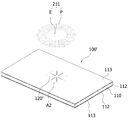
- Magnetic field shielding sheets 100 and 100 ′ include a sheet body 110, through portions 120 and 120 ′, and cracks 130 as shown in FIGS. 1 and 5.
- the sheet body 110 may be made of a material having magnetic properties so as to shield a magnetic field generated from the antennas 211 and 212.
- the antennas 211 and 212 may include a hollow portion E having a predetermined area at a central portion and a pattern portion P formed to surround the hollow portion E with a predetermined number of turns.
- the antennas 211 and 212 are antenna patterns in which a pattern portion P is patterned so that a hollow portion E having a predetermined area is formed on at least one surface of the circuit board 210 (see FIGS. 10 and 11 ).
- it may be a flat coil in which a conductive member having a predetermined wire diameter is wound a plurality of times so that a hollow portion E having a predetermined area is formed in the center portion to form the pattern portion P.
- the antennas 211 and 212 may be a wireless power transmission antenna 211 for transmitting or receiving wireless power, an MST antenna for magnetic payment, or an NFC antenna 212 for short-range communication.
- the antennas 211 and 212 may be configured as a combo type including two or more of the above-described wireless power transmission antenna 212, MST antenna, and NFC antenna 212.
- the sheet body 110 may be formed of a material including a metal component so that the crack 130 can be formed from the through portions 120 and 120 ′ together with the through portions 120 and 120 ′.
- the sheet body 110 may be a ribbon sheet 111a including at least one of an amorphous alloy and a nano-crystal alloy, as shown in FIG. 9.
- Such a sheet body 110 may be formed of a single-layered ribbon sheet 111a, but the sheet body 110 is a multilayer in which a plurality of ribbon sheets 111a are stacked in multiple layers via a first adhesive layer 111b. It could be a sheet.
- the multilayer sheet may be a multilayer sheet in which a plurality of ribbon sheets 111a are stacked in two to three layers.
- the total number of stacked multilayer sheets is not limited thereto, and the total number of stacked multilayer sheets may be appropriately changed according to design conditions.
- the sheet body 110 may be a hybrid sheet in which a ribbon sheet of an amorphous alloy and a ribbon sheet of a nano-crystal alloy are combined.
- a protective film 113 may be attached to at least one of the upper and lower surfaces of the sheet body 110 through the second adhesive layer 112.
- the sheet body 110 may maintain a plate shape through the protective film 113.
- the protective film 113 attached to at least one of the upper and lower surfaces of the sheet body 110 may be a removable release film. Through this, when the protective film 113 is removed from the sheet body 110, the second adhesive layer 112 disposed between the sheet body 110 and the protective film 113 may be exposed to the outside.
- the magnetic field shielding sheets 100 and 100 ′ according to an embodiment of the present invention may be attached to other components using the second adhesive layer 112.
- the magnetic field shielding sheets 100 and 100 ′ are provided with through portions 120 and 120 ′ formed in the inner region of the sheet body 110 as shown in FIGS. 2, 3, 6 and 7. ), and a plurality of cracks 130 extending from the through portions 120 and 120 ′.
- the through parts 120 and 120 ′ may be formed to penetrate the sheet body 110, and the plurality of cracks 130 extend from the through parts 120 and 120 ′ to the inside of the sheet body 110 It can be formed to be.
- the plurality of cracks 130 formed from the through portions 120 and 120 ′ may or may not be connected to each other. In addition, only some of the cracks 130 may be connected to each other.
- the through portions 120 and 120 ′ include all of the protective film 113 together with the sheet body 110 It may be formed to penetrate.
- the plurality of cracks 130 are caused from the through parts 120 and 120 ′ through an external force applied to the sheet body 110 while the through parts 120 and 120 ′ are formed in the sheet body 110 It may be formed.
- the magnetic field shielding sheets 100 and 100 ′ can increase the overall resistance through the through portions 120 and 120 ′ formed in the sheet body 110 and a plurality of cracks 130. The effect of eddy current can be reduced.
- the through portions 120 and 120 ′ formed in the sheet body 110 and the plurality of cracks 130 may function as an eddy current reduction means capable of reducing an eddy current.
- the through parts 120 and 120 ′ may be formed to have a predetermined width and length, and may be formed in an appropriate number of one or more.
- the through portions 120 and 120 ′ may be formed to have a length longer than a width.
- the total number of the plurality of cracks 130 may be relatively larger than the total number of the through portions 120 and 120 ′.
- the through portions 120 and 120 ′ may be formed in a linear shape having a length longer than a width.
- the through portions (120, 120') and a plurality of cracks (130) are formed locally for a partial area of the total area of the sheet body (110). Can be.
- the through portions 120 and 120 ′ and the plurality of cracks 130 are localized with respect to a partial area of the total area of the seat body 110 in consideration of an arrangement relationship with the antenna 211 for transmitting or receiving wireless power. Can be formed.
- the pattern part P of the antenna 211 is disposed among the total area of the sheet body 110 as shown in FIGS. 2 and 3 It may be formed in the arrangement area A1.
- the through portion 120 may further include a portion extending from the placement area A1 toward the hollow portion E of the antenna 211 in addition to the placement area A1.
- the through part 120 ′ and the plurality of cracks 130 are formed only in a partial area A2 in which magnetic flux is concentrated among the total area of the sheet body 110 as shown in FIGS. 6 and 7 It could be.
- the magnetic field shielding sheet (100, 100') is a partial area in which the pattern portion (P) of the antenna 211 is disposed or the hollow portion (E) of the antenna 211 Since the through portions 120 and 120' and a plurality of cracks 130 are partially formed only in a partial area corresponding to the sheet, the overall resistance of the sheet itself is increased to minimize the effect of the eddy current, while having a high permeability of 2000 or more in a very thin thickness I can.
- the magnetic field shielding sheets 100 and 100 ′ may have a high permeability of 2000 or more even at a very thin thickness of 55 ⁇ m to 85 ⁇ m.
- the magnetic field shielding sheets 100 and 100 ′ can increase the inductance of the antennas 211 and 212 while implementing a thinner thickness through a very thin thickness.
- the through part 120 and the through part A plurality of cracks 130 extending from 120 may be formed in an arrangement area A1 in which the pattern portion P of the antenna 211 is disposed among the entire area of the sheet body 110.
- the through part 120 is a hollow part of the antenna from the first part 121 formed in the arrangement area A1 where the pattern part P of the antenna is disposed and the first part 121 A second portion 122 extending to a position corresponding to (E) may be further included, and the plurality of cracks 130 may include portions formed from the second portion 122.
- the through part 120 may be formed in plural in the arrangement region A1, and a plurality of through parts formed in the arrangement region A1 ( The 120 may be spaced apart from each other, and the plurality of cracks 130 may extend from the plurality of through portions 120, respectively.
- the plurality of through parts 120 may be formed radially with respect to the center point of the hollow part E of the antenna 211, and the plurality of through parts 120 It can be formed not to be connected.
- the plurality of through parts 120 may be formed radially with respect to the center point of the antenna hollow part E, and at least a part of the plurality of through parts 120 It may be formed to be connected to each other in a region corresponding to the antenna hollow portion (E).
- the plurality of through portions 120 may be formed in a region in which the second portion 122 corresponds to the hollow portion E of the antenna, and the plurality of second portions 122 are hollow antennas. It may be formed to be connected to each other at the center point of the part (E).
- the plurality of through portions 120 may be connected to each other through the second portion 122 to form a single through portion.
- a partial area including a central point connected to each other through the second part 122 at a position corresponding to the hollow part E of the antenna is through the cracks 130 respectively extending from the second part 122 It can also be separated into multiple pieces.
- a partial area including the center point of the hollow portion E within a region corresponding to the antenna hollow portion E may be formed in a shape similar to a sheet formed separately through a conventional flake process.
- the width of the through portions 120 may be 0.1mm to 0.4mm, and the total number of the through portions 120 formed in the sheet body 110 may be 4 to 16.
- the width of the through portion 120 exceeds 0.4 mm, the amount of the magnetic field leaked through the through portion 120 formed in the sheet body 110 may increase, thereby deteriorating the performance of the shielding sheet.
- the width of the through part 120 is less than 0.1 mm, the process of forming the through part 120 in the sheet body 110 is difficult, and productivity may be lowered.
- the total number of the through portions 120 formed in the sheet body 110 is 17 or more compared to when the total number of the through portions 120 formed in the sheet body 110 is 4 to 16 or less. If formed as, the resistance of the sheet itself increases as the total number of the through portions 120 increases, but the additional eddy current reduction effect is insignificant, and it is difficult to implement a high permeability of 2000 or more.
- the total number of the through portions 120 formed in the sheet body 110 is less than 4 compared to the case where the total number of the through portions 120 formed in the sheet body 110 is 4 to 16 or less. If formed as, it is advantageous to realize a high permeability of 2000 or more, but the resistance of the sheet itself is not sufficient, and characteristic deterioration due to eddy current loss may occur.
- the through part 120 ′ and the The plurality of cracks 130 extending from the through part 120 ′ may be formed in a corresponding region A2 corresponding to the hollow part E of the antenna 211 among the total area of the sheet body 110. .
- the through portion 120 ′ may be formed in plural in the corresponding region A2, and a plurality of through portions formed in the corresponding region A2 120' may be spaced apart from each other, and the plurality of cracks 130 may be formed to extend from the plurality of through portions 120', respectively.
- the plurality of through portions 120 ′ may be formed radially with respect to the center point of the corresponding region A2.
- the partial area A2' including the center point of the corresponding area among the total area of the corresponding area A2 is formed through a plurality of cracks 130 respectively extending from the plurality of through portions 120'. Can be separated into pieces.
- the plurality of through parts 120 ′ may be formed radially with respect to the center point of the corresponding region A2, and at least a part of the plurality of through parts 120 ′ may be It can be formed to be connected to each other.
- one end of the plurality of through parts 120 ′ may be connected to each other at a center point of the corresponding region A2.
- the plurality of through portions 120 ′ may be connected to each other to form a single through portion.
- a partial area (A2') including a center point to which the plurality of through portions 120' are connected to each other among the total area of the corresponding area (A2) extends from the plurality of through-sections 120' connected to each other It may be separated into a plurality of pieces through the cracked 130.
- a partial area including the center point of the total area of the corresponding area A2 is separated into a plurality of pieces through a plurality of cracks 130 extending from the plurality of through portions 120 ′, thereby performing a conventional flake process. It may be formed in a shape similar to the sheet formed through separation.
- the width of the through portion 120 ′ may be 0.1mm to 0.4mm.
- the width of the through part 120 ′ exceeds 0.4 mm, the amount of the magnetic field leaked through the through part 120 ′ formed in the sheet body 110 may increase, thereby deteriorating the performance of the shielding sheet. .
- the width of the through part 120 ′ is less than 0.1 mm, the process of forming the through part 120 ′ in the sheet body 110 is difficult, and productivity may be lowered.
- the arrangement of the through portions 120 and 120 ′ in the magnetic field shielding sheets 100 and 100 ′ is not limited thereto, and if formed in the arrangement region A1 or the corresponding region A2, the The through parts 120 and 120 ′ may be formed in various ways.
- the plurality of through portions 120 are the first through portion (120a), the second through portion (120b), the third through portion (120c), as shown in Figure 4 (a) to (f) It may be formed of through portions including at least one or more of the fourth through portions 120d, and the plurality of through portions 120 may be formed in various ways in the above-described arrangement area A1.
- the plurality of through parts 120 ′ may include a first through part 120a ′, a second through part 120b ′, and a third through part as shown in FIGS. 8A to 8F. 120c') may be formed of through portions including at least one type, and the plurality of through portions 120' may be formed in various ways in the above-described corresponding region A2.
- first through portions 120a and 120a' may be linear through portions formed in a direction perpendicular to the width direction or the length direction of the sheet body 110, and the second through portions 120b and 120b' ) May be a linear through part formed in a direction parallel to the width direction or the length direction of the sheet body 110.
- the third through portions 120c and 120c' may be linear through portions formed to be inclined at a predetermined angle with respect to the width direction or the length direction of the sheet body 110, and the fourth through portion 120d is It may be a curved through part formed in an arc shape having a curvature of.
- the method of forming the plurality of through parts 120 and 120 ′ is not limited thereto, and the method of forming the through part 120 of the shape shown in FIGS. 4A to 4F is the through part ( 120 ′), and the method of forming the through portion 120 ′ of the shape shown in FIGS. 8A to 8F may be applied as the forming method of the through portion 120 of FIG. have.
- the magnetic field shielding sheets 100 and 100 ′ may be implemented as wireless power receiving modules 200 and 200 ′ for wireless power transmission.
- the wireless power receiving module (200, 200') is disposed on one surface of the wireless power receiving antenna 211 for receiving wireless power and the wireless power receiving antenna 211 as shown in FIGS. 10 and 11 It may include a magnetic field shielding sheet (100, 100').
- the magnetic field shielding sheets 100 and 100 ′ constituting the wireless power receiving modules 200 and 200 ′ shown in FIGS. 10 and 11 may be the magnetic field shielding sheets 100 and 100 ′ shown in FIGS. 1 to 9.
- the wireless power receiving modules 200 and 200 ′ may include only the antenna 211 for receiving wireless power, but may further include various antennas performing different functions.
- the wireless power receiving module 200 or 200 ′ may further include at least one of an MST antenna for magnetic payment and an NFC antenna 212 for short-range communication in addition to the antenna 211 for receiving wireless power.
- the wireless power receiving modules 200 and 200 ′ may be applied to portable terminal devices such as mobile phones and tablet PCs.
- the magnetic field shielding sheets 100 and 100 ′ described above may be manufactured through the following manufacturing method.
- the manufacturing method of the magnetic field shielding sheet is a step (S1) of preparing a sheet body (M) of a first area as shown in FIG. 12, and the sheet body (M) is first It may include a punching step (S2) and a second punching step (S3) of the sheet body (M).
- the step (S1) of preparing the sheet body M of the first area may be a preparatory step for manufacturing the final product, the shielding sheets 300 and 300 ′, by cutting them into a predetermined size according to the usage and use.
- the shielding sheet 300 may be the magnetic field shielding sheet 100 or 100' described above.
- the shielding sheet 300 may include the sheet body 110 of the second area as shown in FIG. 20, and the sheet body (M) of the first area as shown in FIGS. 18B and 19B. ) Through the first punching step (S2) and the second punching step (S3) of the first area of the sheet body (M) through the above-described through portions (120, 120) on the side of the second area of the sheet body 110 ') and the crack 130 may be formed.
- the sheet body M may be a plate-shaped sheet having a first area, and may be made of a magnetic material.
- the sheet body M of the first area is caused by a plurality of cracks from the through parts 120 and 120 ′ by an external force.
- 130 may be formed of a material including a metal component so that they may be induced, and may be a sheet subjected to heat treatment.
- the sheet body M of the first area may be a ribbon sheet 111a including at least one of an amorphous alloy and a nano-crystal alloy.
- the sheet body (M) of the first area may be formed of a single-layered ribbon sheet (111a), but a plurality of ribbon sheets (111a) are multi-layered sheets stacked in multiple layers through the first adhesive layer (111b). It may be a hybrid sheet in which a ribbon sheet of an amorphous alloy and a ribbon sheet of a nano-crystal alloy are combined.
- the sheet body M of the first area is an amorphous alloy and a nano crystal grain alloy so that the sheet body 110 of the second area constituting the shielding sheet 300, which is a final product, can be composed of a multilayer sheet.
- a plurality of ribbon sheets 111a including at least one of the plurality of ribbon sheets 111a may be multilayered sheets stacked through the first adhesive layer 111b.
- each of the ribbon sheets 111a constituting the sheet body M of the first area may be a heat-treated ribbon sheet, and at least one of the top and bottom surfaces of the sheet body M of the first area
- the protective film 113 may be attached to the second adhesive layer 112 as a medium.
- the protective film 113 may be attached to an upper surface and a lower surface of the sheet body M of the first area, respectively.
- a plurality of ribbon sheets 111a are stacked through the first adhesive layer 111b to form a multilayered sheet of the first area. And attaching the protective film 113 to at least one of the upper and lower surfaces of the multilayer sheet through the second adhesive layer 112 on which the adhesive is applied to both surfaces of the substrate.
- the protective film 113 attached to the sheet body M of the first area may be a removable release film.
- the shielding sheet having the second area (300, 300') may be separated from the sheet body M of the first area with the adhesive layer 112 exposed on one surface thereof.
- the shielding sheets 300 and 300 ′ separated from the sheet body M of the first area may be attached to other components by using the second adhesive layer 112 formed on one surface.
- the sheet body M of the second area is a pair of protective films each attached to the upper and lower surfaces through the second adhesive layer 112 (113) may be included.
- the second adhesive layer 112 may be formed by applying an adhesive on both sides of the substrate.
- the present invention is not limited thereto, and the protective film 113 may be attached to only one of the upper and lower surfaces of the sheet body 110 of the first area through the second adhesive layer 112 ,
- the second adhesive layer 112 may be a liquid or gel adhesive.
- the step (S2) of first punching the sheet body M of the first area is performed while forming the through portions 120 and 120 ′ having a predetermined width and length in the inner region of the sheet body M of the first area. It may be a step of forming a plurality of cracks 130 extending from the through portions 120 and 120 ′.
- the through parts 120 and 120 ′ may be linear through parts having a predetermined width and length.
- the step (S2) of first punching the sheet body (M) of the first area is the outer border (L) defined through the step (S3) of punching the sheet body (M) of the first area to be described later.
- the first punching of the sheet body having the first area (S1) may be performed using the punching apparatus shown in FIG. 13.
- the punching device includes an upper mold 10 for primary punching provided with a plurality of protrusions 12 protruding to a predetermined height on one surface, and the upper mold 10 for primary punching is disposed under the plurality of A plurality of guides for guiding the movement direction of the first punching lower mold 20 and the first punching upper mold 10 provided with a plurality of opening holes 22 penetrating through positions corresponding to the protrusions 12 It may include a bar (G).
- the plurality of protrusions 12 and the plurality of opening holes 22 may have a shape corresponding to the above-described through portions 120 and 120'.
- the plurality of protrusions 12 and the plurality of opening holes 22 may be formed in a linear shape having a predetermined width and length, and may be formed in an appropriate number of one or more.
- the plurality of protrusions 12 and the plurality of opening holes 22 may be formed to have a length longer than a width.
- each of the plurality of protrusions 12 and the plurality of opening holes 22 may be spaced apart from each other as shown in FIGS. 14A and 14B, and may be disposed radially based on a virtual center point. have.
- a first guide hole H1 through which the guide bar G can pass may be formed at the side of the upper mold 10 for primary punching, and the guide hole H1 may be formed at the side of the sheet body M of the first area.
- At least one second guide hole H2 through which the bar G can pass may be formed through.
- the movement direction of the first punching upper mold 10 may be guided along the guide bar G, and the first When the guide bar G is inserted into the second guide hole H2, the sheet body M having an area may be prevented from flowing.
- the sheet body (M) of the first area is the upper mold for primary punching 10 and the lower mold for primary punching in a state in which the guide bar (G) is fitted in at least one second guide hole (H2). It may be disposed so as to be positioned between (20), and one surface may be pressed through the movement of the upper mold 10 for primary punching.
- the protrusion 12 can press the sheet body M of the first area, and the sheet body of the first area ( On the M) side, through portions 120 and 120 ′ may be formed at positions corresponding to the protrusions 12 by pressing the protrusions 12.
- a plurality of cracks 130 caused by a pressing force transmitted from the protrusion 12 may be formed on the edge side of the through parts 120 and 120 ′ to form the through parts 120 and 120 ′.
- the sheet body M of the first area Through portions 120 and 120 ′ having a predetermined width and length may be formed at a position corresponding to the protrusion 12 in the inner region of the.
- the protrusions 12 and opening holes 22 provided in the upper mold 10 for the first punching and the lower mold 20 for the first punching respectively.
- the through part 120 of the shape shown in FIG. 18A may be formed or the through part 120 ′ in the shape of FIG. 19A may be formed.
- cracks 130 of the shape shown in FIG. 2 may be formed around the penetration portion 120 of the shape shown in FIG. 18A, and may be formed by being induced from the penetration portion 120, and the penetration of the shape shown in FIG. 19A.
- Cracks 130 of the shape shown in FIG. 6 may be formed around the part 120 ′ by being induced from the through part 120 ′.
- the cut piece separated from the sheet body M of the first area may fall downward through the opening hole 22.
- a plurality of cracks 130 caused by the through parts 120 and 120 ′ in the punching process of forming the through parts 120 and 120 ′ having a predetermined width and length. ) Can be formed, so that the through part and the crack caused by it can be formed only in a partial area of the total area of the final product, the shielding sheet 300.
- the shielding sheet 300 produced through the method of manufacturing a magnetic field shielding sheet according to an embodiment of the present invention may have a very thin thickness and can implement a high permeability of 2000 or more.
- the shielding sheet 300 produced through the method of manufacturing a magnetic field shielding sheet according to an embodiment of the present invention is provided through the cracks 130 caused by the through parts 120 and 120 ′ and the through parts 120 and 120 ′. Since the resistance can be increased, loss due to eddy current can be reduced, and the transmission efficiency of the antenna can be increased by increasing the Q value.
- the protrusion 12 of the upper mold 10 for primary punching and the opening hole 22 of the lower mold 20 for primary punching are through portions 120 and 120' formed in the shielding sheet 300, which is a final product. It can be appropriately changed according to the shape of ).
- the protrusion 12 ′ of the upper mold 10 ′ for primary punching and the opening hole 22 ′ of the lower mold 20 ′ for primary punching may be formed in the shapes shown in FIGS. 15A and 15B. I can.
- the plurality of protrusions 12 ′ and the plurality of opening holes 22 ′ may be provided in a plurality in the inner regions of the upper mold 10 ′ for primary punching and the lower mold 20 ′ for primary punching, , One end can be connected to each other to form one.
- each of the plurality of protrusions 12 ′ and the plurality of opening holes 22 ′ may be spaced apart from each other, and may be disposed radially based on a virtual center point, and the plurality of protrusions 12 ') and each of the plurality of opening holes 22' may be at least partially connected to each other.
- the sheet body of the first area Penetrating portions 120 and 120 ′ having a predetermined width and length may be formed in a position corresponding to the protrusion 12 ′ in the inner region of (M).
- a protrusion 12 ′ and an opening hole provided in the upper mold 10 ′ for primary punching and the lower mold 20 ′ for primary punching respectively.
- the through portion 120 of the shape shown in FIG. 3 and a plurality of cracks 130 caused by the through portion 120 may be formed, or the penetration of the shape shown in FIG. 7 A plurality of cracks 130 caused by the portion 120 ′ and the through portion 120 ′ may be formed.
- the protrusions 12 and 12 ′ of the upper molds 10 and 10 ′ for primary punching and the opening holes 22 and 22 ′ of the lower molds 20 and 20 ′ for primary punching It may be appropriately changed according to the shape of the penetration part formed in the final product, the shielding sheet 300. That is, the protrusions 12 and 12 ′ of the upper molds 10 and 10 ′ for primary punching and the opening holes 22 and 22 ′ of the lower molds 20 and 20 ′ for primary punching are shown in FIGS. 4 and 8. It may be configured to correspond to the through portions 120 and 120 ′ of various types shown in FIG.
- each of the plurality of protrusions 12 and 12 ′ and the plurality of opening holes 22 and 22 ′ may be disposed radially based on a virtual center point, and the first area of the sheet body M It may be arranged in parallel or perpendicular to the width direction or the length direction.
- each of the plurality of protrusions 12 and 12 ′ and the plurality of opening holes 22 and 22 ′ may be arranged to be inclined at a predetermined angle with respect to the width direction or the length direction of the sheet body M of the first area.
- it may be formed in an arc shape having a predetermined length.
- each of the plurality of protrusions 12 and 12 ′ and the plurality of opening holes 22 and 22 ′ may be a combination of at least two of the above-described four methods.
- the first punching upper mold (10") used in the first punching step (S1) of the first area of the sheet body forms the through part 120 in the first area of the sheet body (M)
- it may be configured to remove the cut piece C separated from the sheet body M of the first area from the sheet body M of the first area.
- protrusions 12 and 12 ′ in the upper molds 10 and 10 ′ for primary punching described above may be changed to the shape shown in FIG. 16.
- the upper mold 10" for primary punching is a ring-shaped edge blade 12" protruding from one surface and a separating member protruding from the inside of the edge blade 12" (14) may be included.
- the separating member 14 may be formed in a plane having a predetermined width and length, and the width and length of the separating member 14 are relatively smaller than the width and length of the rim blade 12"
- the separating member 14 may be formed to protrude from the inner bottom surface of the rim blade 12" to a certain height, and the protruding height of the separating member 14 is the rim blade 12" It may be the same as the height of or a height relatively lower than the edge blade (12").
- edge blade 12" may have a size corresponding to the through portions 120 and 120'.
- the edge blade 12" is a penetration part having a predetermined width and length. (120, 120') can be formed, and the separating member 14 is cut from the sheet body M of the first area through the edge blade 12" to form the through part 120, 120'. The incision can be pressed downward.
- the cut piece cut from the sheet body M of the first area through the edge blade 12" can be separated from the sheet body M of the first area through the separating member 14
- the cut pieces separated from the sheet body M of the first area may fall downward through the opening holes 22 and 22 ′ of the lower mold 20 for primary punching.
- processing of forming the through parts 120 and 120 ′ and the cracks 130 inside the sheet body M and forming the through parts 120 and 120 ′ may be performed together.
- a shielding sheet 300 having a second area that is relatively narrower than the first area of the sheet body M is transferred to the sheet body of the first area ( It may be a step of forming from M).
- the second punching of the sheet body of the first area may be a step of processing the sheet body M of the first area to the size of the shielding sheet 300, which is a final product, and the first It may be a step of forming an outer border L of the shielding sheet 300 having a second area from the sheet body M of the area, and the shielding sheet 300, which is a final product, is formed along the outer border L. It may be a step of processing so that it can be separated from the sheet body M of the first area.
- the outer border L may be formed from the sheet body M of the first area to include the through portions 120 and 120 ′ formed through the upper mold 10 for primary punching.
- the second punching of the sheet body having the first area (S3) may be performed using the second punching mold 30 shown in FIG. 17.
- the second punching mold 30 may include at least one outer edge blade 32 protruding to a predetermined height on one surface, and the outer edge blade 32 has a ring shape with an empty inside. Can be formed.
- the second punching mold 30 is a first guide hole through which the guide bar G passes so that movement can be guided through the guide bar G, similar to the above-described upper mold 10 for primary punching. H1) may be included.
- An outer border (L) may be formed that surrounds and defines the second area.
- the shielding sheet 300 which is the final product, is the sheet body M of the first area.
- the sheet body M of the first area is a second adhesive layer on the upper and lower surfaces of the sheet body M as described above ( 112a, 112b) may include a pair of protective films (113a, 113b) each attached via the medium, the outer border (L) formed through the second punching mold 30 is the sheet body of the first area It may be formed to penetrate both (M) and the second adhesive layer (112a, 112b), the outer border (L) is on the side of the protective film (113b) attached to the lower surface of the sheet body (M) of the first area May not be formed.
- the outer border L has a first area of the sheet body M, the second adhesive layers 112a and 112b, and the protective film 113a attached to the upper surface of the sheet body M. ) May be formed so that the protective film 113b attached to the lower surface of the sheet body M does not penetrate.
- the The protective film 113b attached to the lower surface of the sheet body M of the first area can serve as a tray that maintains the state in which the plurality of shielding sheets 300 having the second area on one surface are attached. have.
- the shielding sheet 300 having a second area is separated from the sheet body M of the first area, the shielding sheet 300 of the second area separated from the sheet body M of the first area
- the second adhesive layer 112b may be exposed to the outside on one side.
- the user separates the shielding sheet 300 of the second area from the sheet body M of the first area individually and then shields the other parts by using the second adhesive layer 112b exposed to the outside.
- the sheet 300 may be attached or other components may be attached to the shielding sheet 300.
- the method of forming the outer frame L described above is not limited thereto, and the outer frame L formed in the step (S3) of secondary punching the sheet body of the first area is the sheet body of the first area. It may be formed so that the shielding sheet 300 can be completely separated from (M).
- the outer border L formed through the second punching mold 30 is the sheet body M of the first area, the second adhesive layers 112a and 112b, and the sheet body M of the first area. It may be formed to penetrate all of the pair of protective films 113a and 113b attached to the upper and lower surfaces.
- the through portions 120 and 120 ′ formed in the step (S2) of the first punching of the first area of the sheet body may be partially formed only on a partial area of the total area of the final product, the shielding sheet 300, as described above. I can.
- the through part 120 may be formed in a partial area where the pattern part P of the antenna 211 is disposed among the entire area of the shielding sheet 300 as a final product, as shown in FIG. 18B,
- a partial area in which the pattern portion P of the antenna 211 is disposed may be the above-described placement area A1.
- the shielding sheet 300 separated from the sheet body M of the first area is only a partial area corresponding to the pattern part P of the antenna 211 of the total area of the shielding sheet 300
- a crack 130 caused by the through part 120 may be formed together with the through part 120.
- the through portion 120 formed on a partial area corresponding to the pattern portion P of the antenna 211 may be formed in various ways shown in FIGS. 2 to 4 as described above.
- the through part 120 ′ formed in the step (S2) of first punching the sheet body of the first area has a magnetic flux among the total area of the shielding sheet 300, which is a final product, as shown in FIG. 19B. It may be formed only in a concentrated area, and the partial area in which the magnetic flux is concentrated may be a corresponding area A2 corresponding to the hollow portion E of the antenna 211 as described above.
- the shielding sheet 300 separated from the sheet body M of the first area is only for a partial area corresponding to the hollow part E of the antenna 211 of the total area of the shielding sheet 300
- a crack 130 caused by the through part 120 ′ may be formed together with the through part 120 ′.
- the through portion 120 ′ formed for a partial area corresponding to the hollow portion E of the antenna 211 may be formed in various ways shown in FIGS. 6 to 8 as described above. .
Landscapes
- Engineering & Computer Science (AREA)
- Power Engineering (AREA)
- Computer Networks & Wireless Communication (AREA)
- Physics & Mathematics (AREA)
- Electromagnetism (AREA)
- Signal Processing (AREA)
- Microelectronics & Electronic Packaging (AREA)
- Manufacturing & Machinery (AREA)
- Shielding Devices Or Components To Electric Or Magnetic Fields (AREA)
Abstract
자기장 차폐시트가 제공된다. 본 발명의 예시적인 실시예에 따른 자기장 차폐시트는 중앙부에 소정의 면적을 갖는 중공부 및 상기 중공부를 둘러싸는 패턴부를 포함하는 안테나용 자기장 차폐시트로서, 비정질 합금 및 나노결정립 합금 중 적어도 1종 이상을 포함하는 리본시트로 형성되는 시트본체; 상기 시트본체 중 상기 패턴부와 대응되는 영역에 형성되는 복수 개의 관통부; 및 상기 관통부로부터 연장형성되는 다수의 크랙;을 포함한다.
Description
본 발명은 자기장 차폐시트 및 이의 제조방법에 관한 것이다.
근거리 무선통신(NFC) 및 무선 충전은 본질적으로 비접촉식 전송방식이다. 이러한 비접촉식 전송방식은 자기장을 송출하거나 수신하는 안테나와, 자기장을 원활하게 송신하거나 수신할 수 있도록 안테나의 일면에 배치되는 자기장 차폐시트를 통해 구현된다.
통상적으로 자기장 차폐시트로는 비정질 리본시트, 페라이트 시트, 또는 폴리머 시트와 같은 자성재질로 이루어진 시트가 사용된다.
한편, 자기장 차폐시트는 와전류(Eddy Current)에 의한 손실을 크게 줄이거나 시트 자체의 유연성을 개선할 수 있도록 다수의 조각으로 분리형성된 형태의 시트가 활용되고 있다.
일례로, 상기 자기장 차폐시트는 플레이크 공정을 통해 다수 개의 조각으로 분리형성될 수 있다. 이와 같은 플레이크 공정은 외면에 복수의 요철 또는 구형 볼이 형성된 금속롤러와, 고무롤러를 통해 수행될 수 있다.
즉, 상기 금속롤러와 고무롤러가 대향배치된 상태에서 금속롤러 및 고무롤러 사이로 자기장 차폐시트를 복수 회 통과시키면 자기장 차폐시트는 다수 개의 조각으로 분리형성될 수 있다.
이에 따라, 다수 개의 조각으로 분리형성된 자기장 차폐시트를 제조하기 위해서는 시트 자체를 복수 개의 조각으로 분리하기 위한 별도의 플레이크 공정이 수반되므로 생산단가를 증가시키는 문제가 있다.
한편, 한 쌍의 롤러를 통해 수행되는 플레이크 공정에서 자기장 차폐시트는 한 쌍의 롤러 사이를 통과하기 때문에 시트의 전체 면적이 한 쌍의 롤러를 통해 가압된다. 이에 따라, 플레이크 공정을 통해 생산된 자기장 차폐시트는 시트 전체가 복수 개의 조각으로 분리형성될 수밖에 없다.
또한, 종래의 플레이크 공정을 통해 복수 개의 조각으로 분리형성된 자기장 차폐시트는 플레이크 공정이 복수 회 수행되어야 균일한 특성을 가질 수 있다.
그러나 플레이크 공정이 반복적으로 수행될수록 서로 분리된 조각의 사이즈는 작아지지만 분리된 조각의 전체개수는 증가한다. 이에 따라, 플레이크 공정이 반복적으로 수행될수록 차폐시트 자체의 저항은 증가되기 때문에 와전류에 의한 영향을 줄일 수는 있으나 차폐시트의 투자율은 1500 이하로 떨어지는 문제가 있다.
이로 인해, 차폐시트 자체의 저항을 증가시키면서도 2000 이상의 고투자율을 가지는 자기장 차폐시트를 구현하기 위해서는 자기장 차폐시트의 전체두께를 증가시켜야 하는 문제가 있다.
본 발명은 상기와 같은 점을 감안하여 안출한 것으로, 전체면적 중 일부 영역에만 국부적으로 관통부 및 이에 의해 유발된 크랙을 형성함으로써 매우 얇은 두께를 가지면서도 2000 이상의 고투자율을 구현할 수 있는 자기장 차폐시트 및 이의 제조방법을 제공하는데 그 목적이 있다.
또한, 본 발명은 별도의 플레이크 공정을 수행하지 않더라도 전체면적 중 안테나와 대응되는 영역에 크랙을 선택적으로 형성할 수 있는 자기장 차폐시트의 제조방법을 제공하는데 다른 목적이 있다.
상술한 목적을 달성하기 위하여 본 발명은 중앙부에 소정의 면적을 갖는 중공부 및 상기 중공부를 둘러싸는 패턴부를 포함하는 안테나용 자기장 차폐시트로서, 비정질 합금 및 나노결정립 합금 중 적어도 1종 이상을 포함하는 리본시트로 형성되는 시트본체; 상기 시트본체 중 상기 패턴부와 대응되는 영역에 형성되는 복수 개의 관통부; 및 상기 관통부로부터 연장형성되는 다수의 크랙;을 포함하는 자기장 차폐시트를 제공한다.
또한, 상기 관통부는 폭보다 길이가 더 길게 형성될 수 있다.
또한, 상기 복수 개의 관통부들은 서로 간격을 두고 이격배치될 수 있다.
또한, 상기 관통부는 상기 패턴부와 대응되는 영역에 형성되는 제1부분과 상기 제1부분으로부터 상기 안테나의 중공부와 대응되는 영역으로 연장되는 제2부분을 포함할 수 있다. 이때, 상기 복수 개의 관통부들은 상기 제2부분을 통해 서로 연결될 수 있다.
또한, 상기 복수 개의 관통부는 각각의 제2부분이 상기 안테나 중공부의 중심점에서 서로 연결되도록 형성될 수 있다.
또한, 상기 시트본체는 복수 개의 상기 리본시트가 적어도 2층 이상 적층된 다층시트일 수 있고, 상기 시트본체는 상부면과 하부면 중 적어도 어느 일면에 접착층을 매개로 부착된 보호필름을 포함할 수 있다.
또한, 상기 자기장 차폐시트는 전체두께가 55㎛ 내지 85㎛일 수 있다.
또한, 상기 복수 개의 관통부는, 상기 시트본체의 폭방향 또는 길이방향에 대하여 수직한 방향으로 형성되는 제1관통부; 상기 시트본체의 폭방향 또는 길이방향에 대하여 평행한 방향으로 형성되는 제2관통부; 상기 시트본체의 폭방향 또는 길이방향에 대하여 일정각도 기울어지게 형성되는 제3관통부; 및 소정의 곡률을 갖는 호형으로 형성되는 제4관통부; 중 적어도 1종 이상을 포함할 수 있다.
한편, 본 발명은 중앙부에 소정의 면적을 갖는 중공부 및 상기 중공부를 둘러싸는 패턴부를 포함하는 안테나용 자기장 차폐시트로서, 비정질 합금 및 나노결정립 합금 중 적어도 1종 이상을 포함하는 리본시트가 접착층을 매개로 2층 내지 3층으로 적층된 다층시트로 형성되는 시트본체; 상기 시트본체 중 상기 패턴부와 대응되는 배치영역에 관통형성되고, 폭보다 길이가 더 긴 길이를 가지는 선형으로 형성되는 복수 개의 관통부; 및 상기 관통부로부터 상기 시트본체 측으로 연장형성되는 다수의 크랙;을 포함하며, 상기 복수 개의 관통부 각각은 폭이 0.1mm 내지 0.4mm인 선형으로 형성되고, 상기 복수 개의 관통부는 전체개수가 4개 내지 16개이며 서로 연결되지 않도록 형성되는 자기장 차폐시트를 제공한다.
또한, 본 발명은 중앙부에 소정의 면적을 갖는 중공부 및 상기 중공부를 둘러싸는 패턴부를 포함하는 안테나용 자기장 차폐시트로서, 비정질 합금 및 나노결정립 합금 중 적어도 1종 이상을 포함하는 리본시트로 형성되는 시트본체; 상기 시트본체 중 상기 안테나의 중공부와 대응되는 대응영역에 형성되는 복수 개의 관통부; 및 상기 관통부로부터 연장형성되는 다수의 크랙;을 포함하는 자기장 차폐시트를 제공한다.
이와 같은 경우, 상기 복수 개의 관통부는 상기 대응영역의 중심점을 둘러싸도록 배치될 수 있고, 상기 대응영역 중 상기 대응영역의 중심점을 포함하는 일부영역은 상기 복수 개의 관통부로부터 연장된 다수의 크랙을 통해 복수 개의 조각으로 분리형성될 수 있다.
더욱이, 본 발명은 중앙부에 소정의 면적을 갖는 중공부 및 상기 중공부를 둘러싸는 패턴부를 포함하는 무선전력 수신용 안테나; 및 상기 무선전력 수신용 안테나의 일면에 배치되는 상술한 자기장 차폐시트;를 포함하는 무선전력 수신모듈을 제공한다.
또한, 상술한 무선전력 수신모듈은 휴대단말기기에 적용될 수 있다.
한편, 본 발명은 중앙부에 소정의 면적을 갖는 중공부 및 상기 중공부를 둘러싸는 패턴부를 포함하는 안테나용 자기장 차폐시트의 제조방법으로서, 열처리된 비정질 합금 및 나노결정립 합금 중 적어도 1종 이상을 포함하는 리본시트로 형성된 제1면적의 시트본체를 준비하는 단계; 상기 시트본체의 내측영역에 소정의 폭과 길이를 가지는 관통부를 형성하면서 상기 관통부로부터 연장되는 다수의 크랙들을 형성할 수 있도록 상기 시트본체를 1차 타발하는 단계; 및 상기 관통부를 포함하면서 상기 제1면적보다 상대적으로 좁은 제2면적을 가지는 차폐시트를 형성할 수 있도록 상기 시트본체를 2차 타발하는 단계;를 포함하는 자기장 차폐시트의 제조방법을 제공한다.
일례로, 상기 관통부는 상기 안테나의 패턴부가 배치되는 배치영역에 관통형성될 수 있다.
다른 예로써, 상기 관통부는 상기 안테나의 중공부와 대응되는 대응영역에 관통형성될 수 있다.
또한, 상기 시트본체를 1차 타발하는 단계는, 상기 관통부의 테두리를 형성하기 위한 링형상의 테두리칼날과 상기 테두리칼날을 통해 상기 시트본체로부터 절개된 절개편을 가압하여 분리할 수 있도록 상기 테두리칼날의 내측 영역에 형성되는 분리부재를 포함하는 금형을 통해 수행될 수 있다.
또한, 상기 시트본체를 2차 타발하는 단계는, 상기 차폐시트가 상기 시트본체로부터 분리될 수 있도록 상기 제2면적을 규정하는 외곽테두리를 상기 시트본체에 형성하는 단계일 수 있다.
또한, 상기 시트본체를 준비하는 단계는, 복수 개의 상기 리본시트가 제1접착층을 매개로 다층으로 적층된 다층시트를 형성하는 단계; 및 기재의 양면에 접착제가 도포된 제2접착층을 매개로 상기 다층시트의 하부면에 보호필름을 부착하는 단계를 포함할 수 있고, 상기 외곽테두리는 상기 다층시트 및 제2접착층을 관통하도록 형성될 수 있다.
본 발명에 의하면, 매우 얇은 두께를 가지면서도 2000 이상의 고투자율을 가지는 자기장 차폐시트를 구현할 수 있다.
또한, 본 발명에 의하면, 별도의 플레이크 공정을 수행하지 않더라도 전체면적 중 안테나와 대응되는 면적이나 자속이 집중되는 일부영역에 크랙을 선택적으로 형성할 수 있다. 이를 통해, 설계조건 및 요구사양을 만족하는 차폐시트를 간편하게 제조할 수 있다.
도 1은 본 발명의 일 실시예에 따른 자기장 차폐시트를 나타낸 도면,
도 2는 도 1에서 안테나의 패턴부와 대응되는 배치영역에 형성될 수 있는 관통부 및 관통부로부터 유발된 크랙을 개념적으로 나타낸 도면,
도 3은 도 1에서 안테나의 패턴부와 대응되는 배치영역에 형성될 수 있는 다른 형태의 관통부 및 관통부로부터 유발된 크랙을 개념적으로 나타낸 도면,
도 4는 도 1에서 안테나의 패턴부와 대응되는 배치영역에 형성될 수 있는 다양한 형태의 관통부 및 이로부터 유발된 크랙을 개념적으로 나타낸 도면,
도 5는 본 발명의 다른 실시예에 따른 자기장 차폐시트를 나타낸 도면,
도 6은 도 5에서 안테나의 중공부와 대응되는 대응영역을 확대한 도면으로서, 관통부 및 관통부로부터 유발된 크랙을 개념적으로 나타낸 도면,
도 7은 도 5에서 안테나의 중공부와 대응되는 대응영역에 형성될 수 있는 다른 형태의 관통부 및 관통부로부터 유발된 크랙을 개념적으로 나타낸 도면,
도 8은 도 5에서 안테나의 중공부와 대응되는 대응영역에 형성될 수 있는 다양한 형태의 관통부 및 이로부터 유발된 크랙을 개념적으로 나타낸 도면,
도 9는 본 발명에 따른 자기장 차폐시트의 세부구성을 나타낸 단면도,
도 10은 본 발명의 일 실시예에 따른 무선전력 수신모듈로서, 도 1의 자기장 차폐시트가 적용된 무선전력 수신모듈을 나타낸 도면,
도 11은 본 발명의 다른 실시예에 따른 무선전력 수신모듈로서, 도 5의 자기장 차폐시트가 적용된 무선전력 수신모듈을 나타낸 도면,
도 12는 본 발명의 일 실시예에 따른 자기장 차폐시트의 제조방법을 나타낸 순서도,
도 13은 본 발명의 일 실시예에 따른 자기장 차폐시트의 제조방법에서 1차 타발하는 단계에 사용될 수 있는 금형의 일형태를 개념적으로 나타낸 도면,
도 14a 및 도 14b는 도 13에 적용될 수 있는 금형을 나타낸 평면도로서, 도 14a는 1차타발용 상부금형의 평면도이고, 도 14b는 1차타발용 하부금형의 평면도,
도 15a 및 도 15b는 도 13에 적용될 수 있는 금형의 다른 형태를 나타낸 평면도로서, 도 15a는 1차타발용 상부금형의 평면도이고, 도 15b는 1차타발용 하부금형의 평면도,
도 16은 도 13에 적용될 수 있는 1차타발용 상부금형의 또 다른 형태를 나타낸 평면도,
도 17은 본 발명의 일 실시예에 따른 자기장 차폐시트의 제조방법에서 2차 타발하는 단계에 사용될 수 있는 금형의 일형태를 나타낸 평면도,
도 18a는 도 14a 및 도 14b의 금형을 이용하여 1차 타발이 완료된 상태의 다층시트를 나타낸 평면도이고, 도 18b는 도 18a를 도 17의 금형을 이용하여 2차 타발이 완료된 상태의 다층시트를 나타낸 평면도,
도 19a는 도 15a 및 도 15b의 금형을 이용하여 1차 타발이 완료된 상태의 다층시트를 나타낸 평면도이고, 도 19b는 도 19a를 도 17의 금형을 이용하여 2차 타발이 완료된 상태의 다층시트를 나타낸 평면도, 그리고,
도 20은 도 18b 및 도 19b에서 A-A 부분을 발췌한 단면도이다.
이하, 첨부한 도면을 참고로 하여 본 발명의 실시예에 대하여 본 발명이 속하는 기술분야에서 통상의 지식을 가진 자가 용이하게 실시할 수 있도록 상세히 설명한다. 본 발명은 여러 가지 상이한 형태로 구현될 수 있으며 여기에서 설명하는 실시예에 한정되지 않는다. 도면에서 본 발명을 명확하게 설명하기 위해서 설명과 관계없는 부분은 생략하였으며, 명세서 전체를 통하여 동일 또는 유사한 구성요소에 대해서는 동일한 참조부호를 부가한다.
본 발명의 일 실시예에 따른 자기장 차폐시트(100,100')는 도 1 및 도 5에 도시된 바와 같이 시트본체(110), 관통부(120,120') 및 크랙(130)을 포함한다.
상기 시트본체(110)는 안테나(211,212)로부터 발생되는 자기장을 차폐할 수 있도록 자성을 갖는 재질로 이루어질 수 있다.
여기서, 상기 안테나(211,212)는 중앙부에 소정의 면적을 갖는 중공부(E)와 상기 중공부(E)를 소정의 턴수로 감싸도록 형성된 패턴부(P)를 포함할 수 있다.
이와 같은 경우, 상기 안테나(211,212)는 회로기판(210, 도 10 및 도 11 참조)의 적어도 일면에 소정의 면적을 갖는 중공부(E)가 형성되도록 패턴부(P)가 패턴형성된 안테나 패턴일 수도 있고, 중앙부에 소정의 면적을 갖는 중공부(E)가 형성되도록 소정의 선경을 갖는 도전성부재가 복수 회 권선되어 패턴부(P)를 형성하는 평판형코일일 수도 있다.
또한, 상기 안테나(211,212)는 무선전력을 송신하거나 수신하는 무선전력 전송용 안테나(211)일 수도 있고 마그네틱 결제를 위한 MST 안테나일 수도 있으며, 근거리 통신을 위한 NFC 안테나(212)일 수도 있다.
더불어, 상기 안테나(211,212)는 상술한 무선전력 전송용 안테나(212), MST 안테나 및 NFC 안테나(212) 중 둘 이상을 포함하는 콤보형으로 구성될 수도 있다.
이때, 상기 시트본체(110)는 상기 관통부(120,120')와 함께 상기 관통부(120,120')로부터 크랙(130)이 형성될 수 있도록 금속성분을 포함하는 재질로 형성될 수 있다.
일례로, 상기 시트본체(110)는 도 9에 도시된 바와 같이 비정질 합금 및 나노 결정립 합금 중 적어도 1종 이상을 포함하는 리본시트(111a)일 수 있다.
이와 같은 시트본체(110)는 단층의 리본시트(111a)로 형성될 수도 있으나, 상기 시트본체(110)는 복수 개의 리본시트(111a)가 제1접착층(111b)을 매개로 다층으로 적층된 다층시트일 수도 있다. 이와 같은 경우, 상기 다층시트는 복수 개의 리본시트(111a)가 2층 내지 3층으로 적층된 다층시트일 수 있다. 그러나 상기 다층시트의 전체 적층수를 이에 한정하는 것은 아니며, 설계조건에 따라 다층시트의 전체적층수는 적절하게 변경될 수 있다.
또한, 상기 시트본체(110)는 비정질 합금의 리본시트와 나노 결정립 합금의 리본시트가 조합된 하이브리드 시트일 수도 있다.
이때, 상기 시트본체(110)의 상부면과 하부면 중 적어도 어느 일면에는 보호필름(113)이 제2접착층(112)을 매개로 부착될 수 있다.
이에 따라, 상기 시트본체(110)가 상기 관통부(120,120')로부터 연장된 크랙(130)을 포함하더라도 상기 시트본체(110)는 상기 보호필름(113)을 통해 판상의 형태를 유지할 수 있다.
여기서, 상기 시트본체(110)의 상부면과 하부면 중 적어도 일면에 부착되는 보호필름(113)은 제거가능한 릴리즈필름일 수 있다. 이를 통해, 상기 시트본체(110)로부터 상기 보호필름(113)을 제거하면 상기 시트본체(110)와 보호필름(113) 사이에 배치된 제2접착층(112)이 외부로 노출될 수 있기 때문에 본 발명의 일 실시예에 따른 자기장 차폐시트(100,100')는 상기 제2접착층(112)을 이용하여 다른 부품에 부착될 수 있다.
이때, 본 발명의 일 실시예에 따른 자기장 차폐시트(100,100')는 도 2, 도 3, 도 6 및 도 7에 도시된 바와 같이 상기 시트본체(110)의 내측영역에 형성된 관통부(120,120')와, 상기 관통부(120,120')로부터 연장형성된 다수의 크랙(130)을 포함할 수 있다.
일례로, 관통부(120,120')는 상기 시트본체(110)를 관통하도록 형성될 수 있으며, 상기 다수의 크랙(130)은 상기 관통부(120,120')로부터 상기 시트본체(110)의 내측으로 연장되도록 형성될 수 있다.
이와 같은 경우, 상기 관통부(120,120')로부터 형성된 다수의 크랙(130)들은 서로 연결될 수도 있고 연결되지 않을 수도 있다. 또한, 상기 다수의 크랙(130)들 중 일부의 크랙들만 서로 연결될 수도 있다.
여기서, 상술한 바와 같이 상기 보호필름(113)이 상기 시트본체(110)의 적어도 일면에 부착된 경우, 상기 관통부(120,120')는 상기 시트본체(110)와 더불어 보호필름(113)을 모두 관통하도록 형성될 수도 있다.
또한, 상기 다수의 크랙(130)들은 상기 관통부(120,120')가 상기 시트본체(110)에 형성되는 과정에서 상기 시트본체(110)에 가해지는 외력을 통해 상기 관통부(120,120')로부터 유발되어 형성된 것일 수 있다.
이에 따라, 본 발명의 일 실시예에 따른 자기장 차폐시트(100,100')는 상기 시트본체(110)에 형성된 관통부(120,120') 및 다수의 크랙(130)을 통하여 전체적인 저항이 증가될 수 있기 때문에 와전류에 의한 영향이 줄어들 수 있다.
즉, 상기 시트본체(110)에 형성된 관통부(120,120') 및 다수의 크랙(130)은 와전류를 감소시킬 수 있는 와전류저감수단으로서 기능할 수 있다.
여기서, 상기 관통부(120,120')는 소정의 폭과 길이를 갖도록 형성될 수 있고, 하나 이상의 적절한 개수로 형성될 수 있다. 또한, 상기 관통부(120,120')는 폭보다 길이가 더 긴 길이를 갖도록 형성될 수 있다. 더불어, 상기 다수의 크랙(130)은 전체개수가 상기 관통부(120,120')의 전체개수보다 상대적으로 더 많은 개수일 수 있다.
비제한적인 일례로써, 상기 관통부(120,120')는 폭보다 길이가 더 긴 길이를 가지는 선형으로 형성될 수 있다.
이때, 본 발명의 일 실시예에 따른 자기장 차폐시트(100,100')는 상기 관통부(120,120') 및 다수의 크랙(130)이 상기 시트본체(110)의 전체면적 중 일부면적에 대해서 국부적으로 형성될 수 있다.
즉, 상기 관통부(120,120') 및 다수의 크랙(130)은 무선전력을 송신하거나 수신하는 안테나(211)와의 배치관계를 고려하여 상기 시트본체(110)의 전체면적 중 일부면적에 대해서 국부적으로 형성될 수 있다.
일례로, 상기 관통부(120) 및 다수의 크랙(130)은 도 2 및 도 3에 도시된 바와 같이 상기 시트본체(110)의 전체면적 중 상기 안테나(211)의 패턴부(P)가 배치되는 배치영역(A1)에 형성될 수 있다. 이와 같은 경우, 상기 관통부(120)는 상기 배치영역(A1)과 더불어 상기 배치영역(A1)으로부터 안테나(211)의 중공부(E) 측으로 연장되는 부분을 더 포함할 수도 있다.
다른 예로써, 상기 관통부(120') 및 다수의 크랙(130)은 도 6 및 도 7에 도시된 바와 같이 상기 시트본체(110)의 전체면적 중 자속이 집중되는 일부면적(A2)에만 형성될 수도 있다.
이를 통해, 본 발명의 일 실시예에 따른 자기장 차폐시트(100,100')는 전체면적 중 상기 안테나(211)의 패턴부(P)가 배치되는 일부면적 또는 상기 안테나(211)의 중공부(E)와 대응되는 일부면적에만 부분적으로 관통부(120,120') 및 다수의 크랙(130)이 형성되기 때문에 시트 자체의 전체적인 저항을 증가시켜 와전류에 의한 영향을 최소화하면서도 매우 얇은 두께에서 2000 이상의 고투자율을 가질 수 있다.
비제한적인 일례로써, 본 발명의 일 실시예에 따른 자기장 차폐시트(100,100')는 전체두께가 55㎛ 내지 85㎛인 매우 얇은 두께에서도 2000 이상의 고투자율을 가질 수 있다.
이로 인해, 본 발명의 일 실시예에 따른 자기장 차폐시트(100,100')는 매우 얇은 두께를 통해 박형화를 구현하면서도 상기 안테나(211,212)의 인덕턴스를 증가시킬 수 있다.
구체적으로, 도 1 및 도 10에 도시된 바와 같이 본 발명의 일 실시예에 따른 자기장 차폐시트(100)의 일면에 상기 안테나(211)가 배치되는 경우, 상기 관통부(120) 및 상기 관통부(120)로부터 연장된 다수의 크랙(130)은 상기 시트본체(110)의 전체면적 중 상기 안테나(211)의 패턴부(P)가 배치되는 배치영역(A1)에 형성될 수 있다.
이와 같은 경우, 상기 관통부(120)는 상기 안테나의 패턴부(P)가 배치되는 배치영역(A1)에 형성되는 제1부분(121)과 상기 제1부분(121)으로부터 상기 안테나의 중공부(E)와 대응되는 위치까지 연장되는 제2부분(122)을 더 포함할 수 있으며, 상기 다수의 크랙(130)은 상기 제2부분(122)으로부터 형성된 부분을 포함할 수 있다.
비제한적인 일례로써, 도 2 및 도 3에 도시된 바와 같이 상기 관통부(120)는 상기 배치영역(A1)에 복수 개로 형성될 수 있고, 상기 배치영역(A1)에 형성된 복수 개의 관통부(120)는 서로 간격을 두고 이격배치될 수 있으며, 상기 다수의 크랙(130)은 복수 개의 관통부(120)로부터 각각 연장형성될 수 있다.
이때, 도 2에 도시된 바와 같이 상기 복수 개의 관통부(120)는 상기 안테나(211) 중공부(E)의 중심점을 기준으로 방사상으로 형성될 수 있으며, 상기 복수 개의 관통부(120)는 서로 연결되지 않도록 형성될 수 있다.
또한, 도 3에 도시된 바와 같이 상기 복수 개의 관통부(120)는 상기 안테나 중공부(E)의 중심점을 기준으로 방사상으로 형성될 수 있으며, 상기 복수 개의 관통부(120)는 적어도 일부가 상기 안테나 중공부(E)와 대응되는 영역에서 서로 연결되도록 형성될 수 있다.
이와 같은 경우, 상기 복수 개의 관통부(120)는 상기 제2부분(122)이 상기 안테나의 중공부(E)와 대응되는 영역에 형성될 수 있으며, 복수 개의 제2부분(122)들은 안테나 중공부(E)의 중심점에서 서로 연결되도록 형성될 수 있다.
이를 통해, 상기 복수 개의 관통부(120)는 상기 제2부분(122)을 통하여 서로 연결되어 하나의 관통부로 형성될 수 있다. 여기서, 상기 안테나의 중공부(E)와 대응되는 위치에서 상기 제2부분(122)을 통해 서로 연결된 중심점을 포함하는 일부면적은 상기 제2부분(122)으로부터 각각 연장된 크랙(130)을 통해 복수 개의 조각으로 분리될 수도 있다.
이에 따라, 상기 안테나 중공부(E)와 대응되는 영역 내에서 중공부(E)의 중심점을 포함하는 일부면적은 종래의 플레이크 공정을 통해 분리형성된 시트와 유사한 형태로 형성될 수 있다.
본 실시예에서, 상기 관통부(120)의 폭은 0.1mm 내지 0.4mm일 수 있으며, 상기 시트본체(110)에 형성되는 관통부(120)의 전체개수는 4개 내지 16개일 수 있다.
이는, 상기 관통부(120)의 폭이 0.4mm를 초과하면 상기 시트본체(110)에 형성된 관통부(120)를 통해 누설되는 자기장의 양이 증가하여 차폐시트로서의 성능이 저하될 수 있다.
반면, 상기 관통부(120)의 폭이 0.1mm 미만이면 상기 시트본체(110)에 관통부(120)를 형성하는 공정이 어려워 생산성이 저하될 수 있다.
또한, 상기 시트본체(110)에 형성되는 관통부(120)의 전체개수가 4개 내지 16이하일 때와 비교할 때 상기 시트본체(110)에 형성되는 관통부(120)의 전체개수를 17개 이상으로 형성하면 상기 관통부(120)의 전체개수가 증가할수록 시트 자체의 저항은 증가하지만 추가적인 와전류 저감효과는 미미하며 2000 이상의 고투자율을 구현하기 어려운 문제가 있다.
반면, 상기 시트본체(110)에 형성되는 관통부(120)의 전체개수가 4개 내지 16이하일 때와 비교할 때 상기 시트본체(110)에 형성되는 관통부(120)의 전체개수를 4개 미만으로 형성하면 2000 이상의 고투자율을 구현하는데는 유리하나 시트 자체의 저항이 충분하지 못하여 와전류 손실에 의한 특성열화가 발생할 수 있다.
대안으로, 도 5 및 도 11에 도시된 바와 같이 본 발명의 일 실시예에 따른 자기장 차폐시트(100')의 일면에 상기 안테나(211)가 배치되는 경우, 상기 관통부(120') 및 상기 관통부(120')로부터 연장된 다수의 크랙(130)은 상기 시트본체(110)의 전체면적 중 상기 안테나(211)의 중공부(E)와 대응되는 대응영역(A2)에 형성될 수 있다.
비제한적인 일례로써, 도 6 및 도 7에 도시된 바와 같이 상기 관통부(120')는 상기 대응영역(A2)에 복수 개로 형성될 수 있고, 상기 대응영역(A2)에 형성된 복수 개의 관통부(120')는 서로 간격을 두고 이격배치될 수 있으며, 상기 다수의 크랙(130)은 복수 개의 관통부(120')로부터 각각 연장형성될 수 있다.
이때, 도 6에 도시된 바와 같이 상기 복수 개의 관통부(120')는 상기 대응영역(A2)의 중심점을 기준으로 방사상으로 형성될 수 있다. 이와 같은 경우, 상기 대응영역(A2)의 전체면적 중 상기 대응영역의 중심점을 포함하는 일부영역(A2')은 상기 복수 개의 관통부(120')로부터 각각 연장된 크랙(130)을 통해 복수 개의 조각으로 분리될 수 있다.
또한, 도 7에 도시된 바와 같이 상기 복수 개의 관통부(120')는 상기 대응영역(A2)의 중심점을 기준으로 방사상으로 형성될 수 있으며, 상기 복수 개의 관통부(120')는 적어도 일부가 서로 연결되도록 형성될 수 있다.
이와 같은 경우, 상기 복수 개의 관통부(120')는 일단부가 상기 대응영역(A2)의 중심점에서 서로 연결될 수 있다. 이를 통해, 상기 복수 개의 관통부(120')는 서로 연결되어 하나의 관통부로 형성될 수 있다. 여기서, 상기 대응영역(A2)의 전체면적 중 상기 복수 개의 관통부(120')가 서로 연결된 중심점을 포함하는 일부영역(A2')은 일단이 서로 연결된 복수 개의 관통부(120')로부터 각각 연장된 크랙(130)을 통해 복수 개의 조각으로 분리될 수도 있다.
이를 통해, 상기 대응영역(A2)의 전체면적 중 중심점을 포함하는 일부면적은 상기 복수 개의 관통부(120')로부터 연장된 다수의 크랙(130)을 통해 복수 개의 조각으로 분리됨으로써 종래의 플레이크 공정을 통해 분리형성된 시트와 유사한 형태로 형성될 수 있다.
본 실시예에서, 상기 관통부(120')의 폭은 0.1mm 내지 0.4mm일 수 있다.
이는, 상기 관통부(120')의 폭이 0.4mm를 초과하면 상기 시트본체(110)에 형성된 관통부(120')를 통해 누설되는 자기장의 양이 증가하여 차폐시트로서의 성능이 저하될 수 있다.
반면, 상기 관통부(120')의 폭이 0.1mm 미만이면 상기 시트본체(110)에 관통부(120')를 형성하는 공정이 어려워 생산성이 저하될 수 있다.
그러나 본 발명의 일 실시예에 따른 자기장 차폐시트(100,100')에서 상기 관통부(120,120')의 배치형태를 이에 한정하는 것은 아니며, 상기 배치영역(A1) 또는 대응영역(A2) 내에 형성된다면 상기 관통부(120,120')는 다양한 방식으로 형성될 수 있다.
즉, 상기 복수 개의 관통부(120)는 도 4의 (a) 내지 (f)에 도시된 바와 같이 제1관통부(120a), 제2관통부(120b), 제3관통부(120c) 및 제4관통부(120d) 중 적어도 1종 이상을 포함하는 관통부들로 형성될 수 있으며, 상기 복수 개의 관통부(120)는 상술한 배치영역(A1)에 다양한 방식으로 형성될 수 있다.
또한, 상기 복수 개의 관통부(120')는 도 8의 (a) 내지 (f)에 도시된 바와 같이 제1관통부(120a'), 제2관통부(120b') 및 제3관통부(120c') 중 적어도 1종 이상을 포함하는 관통부들로 형성될 수 있으며, 상기 복수 개의 관통부(120')는 상술한 대응영역(A2)에 다양한 방식으로 형성될 수 있다.
여기서, 상기 제1관통부(120a,120a')는 상기 시트본체(110)의 폭방향 또는 길이방향에 대하여 수직한 방향으로 형성된 선형의 관통부일 수 있고, 상기 제2관통부(120b,120b')는 상기 시트본체(110)의 폭방향 또는 길이방향에 대하여 평행한 방향으로 형성된 선형의 관통부일 수 있다.
또한, 상기 제3관통부(120c,120c')는 상기 시트본체(110)의 폭방향 또는 길이방향에 대하여 일정각도 기울어지게 형성된 선형의 관통부일 수 있으며, 상기 제4관통부(120d)는 소정의 곡률을 갖는 호형으로 형성되는 곡선형의 관통부일 수 있다.
그러나 상기 복수 개의 관통부(120,120')의 형성방식을 이에 한정하는 것은 아니며, 도 4의 (a) 내지 (f)에 도시된 형태의 관통부(120)의 형성방식은 도 5의 관통부(120')의 형성방식으로 적용될 수 있으며, 도 8의 (a) 내지 (f)에 도시된 형태의 관통부(120')의 형성방식은 도 1의 관통부(120)의 형성방식으로 적용될 수도 있다.
상술한 본 발명의 일 실시예에 따른 자기장 차폐시트(100,100')는 무선 전력 전송을 위한 무선전력 수신모듈(200,200')로 구현될 수 있다.
즉, 상기 무선전력 수신모듈(200,200')은 도 10 및 도 11에 도시된 바와 같이 무선전력 수신을 위한 무선전력 수신용 안테나(211)와, 상기 무선전력 수신용 안테나(211)의 일면에 배치되는 자기장 차폐시트(100,100')를 포함할 수 있다.
여기서, 도 10 및 도 11에 도시된 상기 무선전력 수신모듈(200,200')을 구성하는 자기장 차폐시트(100,100')는 도 1 내지 도 9에 도시된 자기장 차폐시트(100,100')일 수 있다.
이와 같은 무선전력 수신모듈(200,200')은 안테나가 상기 무선전력 수신용 안테나(211)만으로 구성될 수도 있으나, 서로 다른 기능을 수행하는 다양한 안테나를 더 포함할 수 있다.
일례로, 상기 무선전력 수신모듈(200,200')은 무선전력 수신용 안테나(211) 이외에 마그네틱 결제를 위한 MST 안테나 및 근거리 통신을 위한 NFC 안테나(212) 중 적어도 어느 하나를 더 포함할 수 있다.
더하여, 상기 무선전력 수신모듈(200,200')은 휴대폰, 태블릿 PC 등과 같은 휴대단말기기에 적용될 수 있다.
한편, 상술한 자기장 차폐시트(100,100')는 아래의 제조방법을 통해 제조될 수 있다.
즉, 본 발명의 일 실시예에 따른 자기장 차폐시트의 제조방법은 도 12에 도시된 바와 같이 제1면적의 시트본체(M)를 준비하는 단계(S1), 상기 시트본체(M)를 1차 타발하는 단계(S2) 및 상기 시트본체(M)를 2차 타발하는 단계(S3)를 포함할 수 있다.
상기 제1면적의 시트본체(M)를 준비하는 단계(S1)는 사용처 및 용도에 맞게 소정의 크기로 절단하여 최종제품인 차폐시트(300,300')를 제조하기 위한 준비단계일 수 있다. 여기서, 상기 차폐시트(300)는 상술한 자기장 차폐시트(100,100')일 수 있다.
즉, 상기 차폐시트(300)는 도 20에 도시된 바와 같이 제2면적의 시트본체(110)를 포함할 수 있으며, 도 18b 및 도 19b에 도시된 바와 같이 상기 제1면적의 시트본체(M)를 1차 타발하는 단계(S2) 및 상기 제1면적의 시트본체(M)를 2차 타발하는 단계(S3)를 통해 상기 제2면적의 시트본체(110) 측에 상술한 관통부(120,120') 및 크랙(130)이 형성될 수 있다.
이에 대한 구체적인 내용은 후술하기로 한다.
이와 같은 시트본체(M)는 제1면적을 갖는 판상의 시트일 수 있으며, 자성을 갖는 재질로 이루어질 수 있다.
이때, 상기 제1면적의 시트본체(M)는 상기 제1면적의 시트본체(M)에 관통부(120,120')를 형성하는 과정에서 외력에 의해 상기 관통부(120,120')로부터 다수의 크랙(130)들이 유발될 수 있도록 금속성분을 포함하는 재질로 형성될 수 있으며 열처리가 수행된 시트일 수 있다.
일례로, 상기 제1면적의 시트본체(M)는 비정질 합금 및 나노 결정립 합금 중 적어도 1종 이상을 포함하는 리본시트(111a)일 수 있다.
여기서, 상기 제1면적의 시트본체(M)는 단층의 리본시트(111a)로 형성될 수도 있으나, 복수 개의 리본시트(111a)가 제1접착층(111b)을 매개로 다층으로 적층된 다층시트일 수 있으며, 비정질 합금의 리본시트와 나노 결정립 합금의 리본시트가 조합된 하이브리드 시트일 수도 있다.
비제한적인 일례로써, 상기 제1면적의 시트본체(M)는 최종제품인 차폐시트(300)를 구성하는 제2면적의 시트본체(110)가 다층시트로 구성될 수 있도록 비정질 합금 및 나노 결정립 합금 중 적어도 1종 이상을 포함하는 복수 개의 리본시트(111a)가 제1접착층(111b)을 매개로 적층된 다층시트일 수 있다.
또한, 상기 제1면적의 시트본체(M)를 구성하는 각각의 리본시트(111a)는 열처리된 리본시트일 수 있으며, 상기 제1면적의 시트본체(M)의 상부면과 하부면 중 적어도 일면에 제2접착층(112)을 매개로 보호필름(113)이 부착된 상태일 수 있다.
바람직하게는, 상기 보호필름(113)은 상기 제1면적의 시트본체(M)의 상부면과 하부면에 각각 부착될 수 있다.
즉, 상기 제1면적의 시트본체(M)를 준비하는 단계(S1)는 복수 개의 리본시트(111a)를 제1접착층(111b)을 매개로 적층하여 다층으로 형성된 제1면적의 다층시트를 형성하는 단계 및 기재의 양면에 접착제가 도포된 제2접착층(112)을 매개로 상기 다층시트의 상부면과 하부면 중 적어도 일면에 보호필름(113)을 부착하는 단계를 포함할 수 있다.
여기서, 상기 제1면적의 시트본체(M)에 부착되는 보호필름(113)은 제거가능한 릴리즈필름일 수 있다.
이를 통해, 후술하는 2차 타발하는 단계(S3)를 통해 상기 제1면적을 갖는 시트본체(M) 측에 제2면적을 규정하는 외곽테두리(L)를 형성하면 상기 제2면적을 갖는 차폐시트(300,300')는 일면에 상기 제접착층(112)이 노출된 상태로 상기 제1면적의 시트본체(M)로부터 분리될 수 있다.
이에 따라, 상기 제1면적의 시트본체(M)로부터 분리된 차폐시트(300,300')는 일면에 형성된 제2접착층(112)을 이용하여 다른 부품을 부착될 수 있다.
비제한적인 일례로써, 도 13의 확대도에 도시된 바와 같이 상기 제2면적의 시트본체(M)는 상부면과 하부면에 제2접착층(112)을 매개로 각각 부착된 한 쌍의 보호필름(113)을 포함할 수 있다. 이와 같은 경우, 상기 제2접착층(112)은 기재의 양면에 접착제가 도포된 것일 수 있다.
그러나 본 발명을 이에 한정하는 것은 아니며, 상기 보호필름(113)은 상기 제1면적의 시트본체(110)의 상부면과 하부면 중 어느 일면에만 제2접착층(112)을 매개로 부착될 수 있으며, 상기 제2접착층(112)은 액상 또는 겔상의 접착제일 수도 있다.
상기 제1면적의 시트본체(M)를 1차 타발하는 단계(S2)는 상기 제1면적의 시트본체(M)의 내측영역에 소정의 폭과 길이를 가지는 관통부(120,120')를 형성하면서 상기 관통부(120,120')로부터 연장되는 다수의 크랙(130)들을 형성하는 단계일 수 있다. 여기서, 상기 관통부(120,120')는 소정의 폭과 길이를 가지는 선형의 관통부일 수 있다.
즉, 상기 제1면적의 시트본체(M)를 1차 타발하는 단계(S2)는 후술할 제1면적의 시트본체(M)를 2차 타발하는 단계(S3)를 통해 규정되는 외곽테두리(L)의 내측 영역에 관통부(120,120')를 형성하는 단계일 수 있으며, 상기 관통부(120,120')와 함께 상기 관통부(120,120')로부터 유발된 다수의 크랙(130)들을 동시에 형성하는 단계일 수 있다.
이와 같은 제1면적의 시트본체를 1차 타발하는 단계(S1)는 도 13에 도시된 타발장치를 이용하여 수행될 수 있다.
일례로, 상기 타발장치는 일면에 소정의 높이로 돌출형성된 복수 개의 돌출부(12)가 구비되는 1차타발용 상부금형(10)과, 상기 1차타발용 상부금형(10)의 하부에 배치되고 상기 복수 개의 돌출부(12)와 대응되는 위치에 관통형성되는 복수 개의 개구홀(22)이 구비되는 1차타발용 하부금형(20) 및 상기 1차타발용 상부금형(10)의 이동방향을 안내하는 복수 개의 가이드바(G)를 포함할 수 있다.
이와 같은 경우, 상기 복수 개의 돌출부(12) 및 복수 개의 개구홀(22)은 상술한 관통부(120,120')와 대응되는 형상을 가질 수 있다.
일례로, 상기 복수 개의 돌출부(12) 및 복수 개의 개구홀(22)은 소정의 폭과 길이를 갖는 선형으로 형성될 수 있으며, 하나 이상의 적절한 개수로 형성될 수 있다. 또한, 상기 복수 개의 돌출부(12) 및 복수 개의 개구홀(22)은 폭보다 길이가 더 긴 길이를 갖도록 형성될 수 있다.
또한, 상기 복수 개의 돌출부(12) 및 복수 개의 개구홀(22) 각각은 도 14a 및 도 14b에 도시된 바와 같이 서로 간격을 두고 이격배치될 수 있으며, 가상의 중심점을 기준으로 방사상으로 배치될 수 있다.
이때, 상기 1차타발용 상부금형(10) 측에는 상기 가이드바(G)가 통과할 수 있는 제1가이드홀(H1)이 각각 형성될 수 있으며, 상기 제1면적의 시트본체(M) 측에는 상기 가이드바(G)가 통과할 수 있는 적어도 하나의 제2가이드홀(H2)이 관통형성될 수 있다.
이에 따라, 상기 1차타발용 상부금형(10)은 상기 가이드바(G)가 상기 제1가이드홀(H1)에 끼워지면 상기 가이드바(G)를 따라 이동방향이 안내될 수 있으며, 상기 제1면적의 시트본체(M)는 상기 가이드바(G)가 상기 제2가이드홀(H2)에 끼워지면 유동이 방지될 수 있다.
이를 통해, 상기 제1면적의 시트본체(M)는 적어도 하나의 제2가이드홀(H2)에 상기 가이드바(G)가 끼워진 상태에서 상기 1차타발용 상부금형(10) 및 1차타발용 하부금형(20) 사이에 위치하도록 배치될 수 있으며, 상기 1차타발용 상부금형(10)의 이동을 통해 일면이 가압될 수 있다.
이에 따라, 1차 타발공정시 상기 1차타발용 상부금형(10)이 하강되면 상기 돌출부(12)는 상기 제1면적의 시트본체(M)를 가압할 수 있으며, 상기 제1면적의 시트본체(M) 측에는 상기 돌출부(12)의 가압을 통해 상기 돌출부(12)와 대응되는 위치에 관통부(120,120')가 형성될 수 있다.
더불어, 상기 관통부(120,120')의 테두리 측에는 상기 관통부(120,120')를 형성하기 위하여 상기 돌출부(12)로부터 전달되는 가압력을 통해 유발된 다수의 크랙(130)들이 형성될 수 있다.
즉, 도 14a 내지 도 14b에 도시된 형태의 1차타발용 상부금형(10) 및 1차타발용 하부금형(20)을 이용하여 1차 타발공정을 수행하면, 상기 제1면적의 시트본체(M)의 내측영역에는 상기 돌출부(12)와 대응되는 위치에 소정의 폭과 길이를 갖는 관통부(120,120')가 형성될 수 있다.
이와 같은 경우, 상기 제1면적의 시트본체(M)의 내측영역에는 상기 1차타발용 상부금형(10) 및 1차타발용 하부금형(20)에 각각 구비되는 돌출부(12) 및 개구홀(22)의 사이즈에 따라 도 18a에 도시된 형태의 관통부(120)가 형성될 수도 있고 도 19a에 형태의 관통부(120')가 형성될 수도 있다.
더불어, 도 18a에 도시된 형태의 관통부(120) 주위에는 도 2에 도시된 형태의 크랙(130)들이 상기 관통부(120)로부터 유발되어 형성될 수 있고, 도 19a에 도시된 형태의 관통부(120') 주위에는 도 6에 도시된 형태의 크랙(130)들이 상기 관통부(120')로부터 유발되어 형성될 수 있다.
여기서, 상기 관통부(120)를 형성하면서 상기 제1면적의 시트본체(M)로부터 분리된 절개편은 상기 개구홀(22)을 통해 하부로 낙하할 수 있다.
이와 같이 본 발명의 일 실시예에 따른 자기장 차폐시트의 제조방법은 소정의 폭과 길이를 가지는 관통부(120,120')를 형성하는 타발과정에서 관통부(120,120')로부터 유발된 다수 개의 크랙(130)들을 형성할 수 있기 때문에 최종제품인 차폐시트(300)의 전체면적 중 일부 영역에만 국부적으로 관통부 및 이에 의해 유발된 크랙을 형성할 수 있다.
이에 따라, 본 발명의 일 실시예에 따른 자기장 차폐시트의 제조방법을 이용하면 설계조건 및 요구사양을 만족하는 차폐시트를 간편하게 제조할 수 있다.
이를 통해, 본 발명의 일 실시예에 따른 자기장 차폐시트의 제조방법을 통해 생산된 차폐시트(300)는 매우 얇은 두께를 가지면서도 2000 이상의 고투자율을 구현할 수 있다.
더불어, 본 발명의 일 실시예에 따른 자기장 차폐시트의 제조방법을 통해 생산된 차폐시트(300)는 상기 관통부(120,120') 및 관통부(120,120')로부터 유발된 크랙(130)들을 통해 전체적인 저항이 증가될 수 있기 때문에 와전류에 의한 손실을 저감할 수 있으며 Q값을 높여 안테나의 전송 효율을 증가시킬 수 있다.
이와 같은 경우, 상기 1차타발용 상부금형(10)의 돌출부(12) 및 상기 1차타발용 하부금형(20)의 개구홀(22)은 최종제품인 차폐시트(300)에 형성되는 관통부(120,120')의 형상에 따라 적절하게 변경될 수 있다.
일례로, 상기 1차타발용 상부금형(10')의 돌출부(12') 및 상기 1차타발용 하부금형(20')의 개구홀(22')은 도 15a 및 도 15b에 도시된 형태로 형성될 수 있다.
즉, 상기 복수 개의 돌출부(12') 및 복수 개의 개구홀(22')은 상기 1차타발용 상부금형(10') 및 1차타발용 하부금형(20')의 내부영역에 복수 개로 구비될 수 있으며, 일단이 서로 연결되어 하나로 구성될 수 있다.
또한, 상기 복수 개의 돌출부(12') 및 복수 개의 개구홀(22') 각각은 서로 간격을 두고 이격배치될 수 있고, 가상의 중심점을 기준으로 방사상으로 배치될 수 있으며, 상기 복수 개의 돌출부(12') 및 복수 개의 개구홀(22') 각각은 적어도 일부가 서로 연결될 수 있다.
이에 따라, 도 15a 및 도 15b에 도시된 형태의 1차타발용 상부금형(10') 및 1차타발용 하부금형(20')을 이용하여 1차 타발공정을 수행하면, 상기 제1면적의 시트본체(M)의 내측영역에는 상기 돌출부(12')와 대응되는 위치에 소정의 폭과 길이를 가지는 관통부(120,120')가 형성될 수 있다.
이와 같은 경우, 상기 제1면적의 시트본체(M)의 내측영역에는 상기 1차타발용 상부금형(10') 및 1차타발용 하부금형(20')에 각각 구비되는 돌출부(12') 및 개구홀(22')의 사이즈에 따라 도 3에 도시된 형태의 관통부(120)와 상기 관통부(120)로부터 유발된 다수의 크랙(130)들이 형성될 수도 있고, 도 7에 도시된 형태의 관통부(120')와 상기 관통부(120')로부터 유발된 다수의 크랙(130)들이 형성될 수도 있다.
더불어, 도면에는 도시하지 않았지만 상기 1차타발용 상부금형(10,10')의 돌출부(12,12') 및 상기 1차타발용 하부금형(20,20')의 개구홀(22,22')은 최종제품인 차폐시트(300)에 형성되는 관통부의 형태에 따라 적절하게 변경될 수 있다. 즉, 상기 1차타발용 상부금형(10,10')의 돌출부(12,12') 및 상기 1차타발용 하부금형(20,20')의 개구홀(22,22')은 도 4 및 도 8에 도시된 다양한 형태의 관통부(120,120')와 대응되도록 구성될 수 있다.
일례로, 상기 복수 개의 돌출부(12,12') 및 복수 개의 개구홀(22,22') 각각은 가상의 중심점을 기준으로 방사상으로 배치될 수도 있고, 상기 제1면적의 시트본체(M)의 폭방향 또는 길이방향과 수직하거나 평행하게 배치될 수도 있다.
또한, 상기 복수 개의 돌출부(12,12') 및 복수 개의 개구홀(22,22') 각각은 상기 제1면적의 시트본체(M)의 폭방향 또는 길이방향에 대하여 일정각도 기울어지게 배치될 수도 있고, 소정의 길이를 갖는 호형의 형상으로 형성될 수도 있다.
더불어, 상기 복수 개의 돌출부(12,12') 및 복수 개의 개구홀(22,22') 각각은 상술한 4가지 방식 중 적어도 2개의 방식이 서로 조합된 형태일 수도 있다.
이를 통해, 상기 제1면적의 시트본체(M)로부터 타발공정을 통해 타발된 차폐시트(300)에는 도 4 및 도 8에 도시된 형태의 다양한 관통부(120,120') 및 크랙(130)이 형성될 수 있다.
한편, 상기 제1면적의 시트본체를 1차 타발하는 단계(S1)에 사용되는 1차타발용 상부금형(10")은 상기 제1면적의 시트본체(M)에 상기 관통부(120)를 형성하는 과정에서 상기 제1면적의 시트본체(M)로부터 분리된 절개편(C)을 상기 제1면적의 시트본체(M)로부터 제거할 수 있도록 구성될 수도 있다.
즉, 상술한 1차타발용 상부금형(10,10')에서 돌출부(12,12')는 도 16에 도시된 형태로 변경될 수 있다.
구체적으로, 도 16에 도시된 바와 같이 1차타발용 상부금형(10")은 일면으로부터 돌출형성되는 링형상의 테두리칼날(12")과 상기 테두리칼날(12")의 내측에 돌출형성되는 분리부재(14)를 포함할 수 있다.
여기서, 상기 분리부재(14)는 소정의 폭과 길이를 갖는 면상으로 형성될 수 있으며, 상기 분리부재(14)의 폭과 길이는 상기 테두리칼날(12")의 폭과 길이보다 상대적으로 작은 크기일 수 있다. 또한, 상기 분리부재(14)는 상기 테두리칼날(12")의 내측 바닥면으로부터 일정높이 돌출되도록 형성될 수 있으며, 상기 분리부재(14)의 돌출높이는 상기 테두리칼날(12")의 높이와 동일하거나 상기 테두리칼날(12")보다 상대적으로 낮은 높이일 수 있다.
더불어, 상기 테두리칼날(12")은 상기 관통부(120,120')와 대응되는 크기일 수 있다.
이에 따라, 1차 타발공정시 상술한 1차타발용 상부금형(10")을 제1면적의 시트본체(M)에 가압하면, 상기 테두리칼날(12")은 소정의 폭과 길이를 갖는 관통부(120,120')를 형성할 수 있으며, 상기 분리부재(14)는 상기 관통부(120,120')를 형성하기 위하여 상기 테두리칼날(12")을 통해 상기 제1면적의 시트본체(M)로부터 절개된 절개편을 하방으로 가압할 수 있다.
이를 통해, 상기 테두리칼날(12")을 통해 상기 제1면적의 시트본체(M)로부터 절개된 절개편은 상기 분리부재(14)를 통해 상기 제1면적의 시트본체(M)로부터 분리될 수 있으며, 상기 제1면적의 시트본체(M)로부터 분리된 절개편은 상기 1차타발용 하부금형(20)의 개구홀(22,22')을 통해 하부로 낙하할 수 있다.
이로 인해, 상술한 1차타발용 상부금형(10")을 이용하면 상기 관통부(120,120')를 형성하는 과정에서 상기 테두리칼날(12")을 통해 상기 제1면적의 시트본체(M)로부터 절개된 절개편을 별도로 분리할 필요없이, 1차 타발과정에서 상기 절개편(C)이 간편하게 제거될 수 있다.
이에 따라, 상술한 1차타발용 상부금형(10")을 이용하면 시트본체(M)의 내측에 관통부(120,120') 및 크랙(130)을 형성하는 가공과 상기 관통부(120,120')를 형성하는 과정에서 생성되는 불필요한 절개편의 제거 작업이 함께 수행될 수 있다.
이를 통해, 상술한 1차타발용 상부금형(10")을 이용하면 상기 관통부(120,120') 및 크랙(130)을 포함하는 차폐시트(300)를 제조하더라도 전체 공정을 간소화시킬 수 있음으로써 생산단가를 줄일 수 있는 장점이 있다.
상기 제1면적의 시트본체를 2차 타발하는 단계(S3)는 상기 시트본체(M)의 제1면적보다 상대적으로 좁은 제2면적을 가지는 차폐시트(300)를 상기 제1면적의 시트본체(M)로부터 형성하는 단계일 수 있다.
즉, 상기 제1면적의 시트본체를 2차 타발하는 단계(S3)는 최종제품인 차폐시트(300)의 크기로 상기 제1면적의 시트본체(M)를 가공하는 단계일 수 있고, 상기 제1면적의 시트본체(M)로부터 제2면적을 가지는 상기 차폐시트(300)의 외곽테두리(L)를 형성하는 단계일 수 있으며, 최종제품인 차폐시트(300)가 상기 외곽테두리(L)를 따라 상기 제1면적의 시트본체(M)로부터 분리될 수 있도록 가공하는 단계일 수 있다.
이와 같은 경우, 상기 외곽테두리(L)는 상기 1차타발용 상부금형(10)을 통해 형성된 관통부(120,120')를 포함하도록 상기 제1면적의 시트본체(M)로부터 형성될 수 있다.
구체적으로, 상기 제1면적의 시트본체를 2차 타발하는 단계(S3)는 도 17에 도시된 2차타발용 금형(30)을 이용하여 수행될 수 있다.
즉, 상기 2차타발용 금형(30)은 일면에 소정의 높이로 돌출형성된 적어도 하나의 외곽테두리용 칼날(32)을 포함할 수 있으며, 상기 외곽테두리용 칼날(32)은 내부가 빈 링형상으로 형성될 수 있다.
또한, 상기 2차타발용 금형(30)은 상술한 1차타발용 상부금형(10)과 마찬가지로 가이드바(G)를 통해 이동이 안내될 수 있도록 상기 가이드바(G)가 통과하는 제1가이드홀(H1)을 포함할 수 있다.
이에 따라, 상기 1차타발용 상부금형(10,10',10")을 통해 관통부(120,120') 및 이로부터 유발된 크랙(130)들이 형성된 제1면적의 시트본체(M) 측에 상기 2차타발용 금형(30)을 가압하면, 상기 제1면적의 시트본체(M) 측에는 도 18b 및 도 19b에 도시된 바와 같이 상기 외곽테두리용 칼날(32)을 통해 상기 복수 개의 관통부(120,120')를 둘러싸면서 제2면적을 규정하는 외곽테두리(L)가 형성될 수 있다.
이를 통해, 상기 외곽테두리(L)를 통해 규정된 제2면적을 가지는 부분을 상기 제1면적의 시트본체(M)로부터 분리하면 최종제품인 차폐시트(300)는 상기 제1면적의 시트본체(M)로부터 제조될 수 있다.
이때, 상기 제1면적의 시트본체를 2차 타발하는 단계(S3)에서 상기 제1면적의 시트본체(M)는 상술한 바와 같이 시트본체(M)의 상부면과 하부면에 제2접착층(112a,112b)을 매개로 각각 부착된 한 쌍의 보호필름(113a,113b)을 포함할 수 있고, 상기 2차타발용 금형(30)을 통해 형성된 외곽테두리(L)는 상기 제1면적의 시트본체(M) 및 제2접착층(112a,112b)을 모두 관통하도록 형성될 수 있으며, 상기 외곽테두리(L)는 상기 제1면적의 시트본체(M)의 하부면에 부착되는 보호필름(113b) 측에는 형성되지 않을 수 있다.
즉, 도 20에 도시된 바와 같이 상기 외곽테두리(L)는 제1면적의 시트본체(M), 제2접착층(112a,112b) 및 시트본체(M)의 상부면에 부착된 보호필름(113a)을 관통하면서 상기 시트본체(M)의 하부면에 부착된 보호필름(113b)은 관통하지 않도록 형성될 수 있다.
이에 따라, 본 발명의 일 실시예에 따른 자기장 차폐시트의 제조방법을 통해 제1면적을 가지는 하나의 시트본체(M)에 제2면적을 가지는 복수 개의 차폐시트(300)를 형성한 경우, 상기 제1면적의 시트본체(M)의 하부면에 부착된 보호필름(113b)은 일면에 제2면적을 가지는 상기 복수 개의 차폐시트(300)가 부착된 상태를 유지하는 트레이로서의 역할을 수행할 수 있다.
또한, 상기 제1면적의 시트본체(M)로부터 제2면적을 가지는 차폐시트(300)를 개별적으로 분리하면 상기 제1면적의 시트본체(M)로부터 분리된 제2면적의 차폐시트(300)는 일면에 제2접착층(112b)이 외부로 노출될 수 있다.
이로 인해, 사용자는 상기 제1면적의 시트본체(M)로부터 상기 제2면적의 차폐시트(300)를 개별적으로 분리한 후 외부로 노출된 제2접착층(112b)을 이용하여 다른 부품에 상기 차폐시트(300)를 부착하거나 상기 차폐시트(300)에 다른 부품을 부착할 수 있다.
그러나 상술한 외곽테두리(L)의 형성방식을 이에 한정하는 것은 아니며, 상기 제1면적의 시트본체를 2차 타발하는 단계(S3)에서 형성되는 외곽테두리(L)는 상기 제1면적의 시트본체(M)로부터 차폐시트(300)가 완전히 분리될 수 있도록 형성될 수도 있다.
즉, 상기 2차타발용 금형(30)을 통해 형성되는 외곽테두리(L)는 상기 제1면적의 시트본체(M), 제2접착층(112a,112b) 및 제1면적의 시트본체(M)의 상부면 및 하부면에 부착된 한 쌍의 보호필름(113a,113b)을 모두 관통하도록 형성될 수도 있다.
한편, 상기 제1면적의 시트본체를 1차 타발하는 단계(S2)에서 형성되는 관통부(120,120')는 상술한 바와 같이 최종제품인 차폐시트(300)의 전체면적 중 일부면적에만 부분적으로 형성될 수 있다.
일례로, 상기 관통부(120)는 도 18b에 도시된 바와 같이 최종제품인 차폐시트(300)의 전체면적 중 상기 안테나(211)의 패턴부(P)가 배치되는 일부면적에 형성될 수 있으며, 상기 안테나(211)의 패턴부(P)가 배치되는 일부면적은 상술한 배치영역(A1)일 수 있다.
이를 통해, 상기 제1면적의 시트본체(M)로부터 분리된 차폐시트(300)는 상기 차폐시트(300)의 전체면적 중 상기 안테나(211)의 패턴부(P)와 대응되는 일부면적에 대해서만 상기 관통부(120)와 함께 상기 관통부(120)로부터 유발된 크랙(130)이 형성될 수 있다.
이와 같은 경우, 상기 안테나(211)의 패턴부(P)와 대응되는 일부면적에 대해서 형성되는 관통부(120)는 상술한 바와 같이 도 2 내지 도 4에 도시된 다양한 방식으로 형성될 수 있다.
다른 예로써, 상기 제1면적의 시트본체를 1차 타발하는 단계(S2)에서 형성되는 관통부(120')는 도 19b에 도시된 바와 같이 최종제품인 차폐시트(300)의 전체면적 중 자속이 집중되는 일부면적에만 형성될 수 있으며, 상기 자속이 집중되는 일부영역은 상술한 바와 같이 상기 안테나(211)의 중공부(E)와 대응되는 대응영역(A2)일 수 있다.
이를 통해, 상기 제1면적의 시트본체(M)로부터 분리된 차폐시트(300)는 상기 차폐시트(300)의 전체면적 중 상기 안테나(211)의 중공부(E)와 대응되는 일부면적에 대해서만 상기 관통부(120')와 함께 상기 관통부(120')로부터 유발된 크랙(130)이 형성될 수 있다.
이와 같은 경우, 상기 안테나(211)의 중공부(E)와 대응되는 일부면적에 대해서 형성되는 관통부(120')는 상술한 바와 같이 도 6 내지 도 8에 도시된 다양한 방식으로 형성될 수 있다.
이상에서 본 발명의 일 실시예에 대하여 설명하였으나, 본 발명의 사상은 본 명세서에 제시되는 실시 예에 제한되지 아니하며, 본 발명의 사상을 이해하는 당업자는 동일한 사상의 범위 내에서, 구성요소의 부가, 변경, 삭제, 추가 등에 의해서 다른 실시 예를 용이하게 제안할 수 있을 것이나, 이 또한 본 발명의 사상범위 내에 든다고 할 것이다.
Claims (17)
- 중앙부에 소정의 면적을 갖는 중공부 및 상기 중공부를 둘러싸는 패턴부를 포함하는 안테나용 자기장 차폐시트로서,비정질 합금 및 나노결정립 합금 중 적어도 1종 이상을 포함하는 리본시트로 형성되는 시트본체;상기 시트본체 중 상기 패턴부와 대응되는 영역에 형성되는 복수 개의 관통부; 및상기 관통부로부터 연장형성되는 다수의 크랙;을 포함하는 자기장 차폐시트.
- 제 1항에 있어서,상기 관통부는 폭보다 길이가 더 길게 형성되는 자기장 차폐시트.
- 제 1항에 있어서,상기 복수 개의 관통부들은 서로 간격을 두고 이격배치되는 자기장 차폐시트.
- 제 1항에 있어서,상기 관통부는 상기 패턴부와 대응되는 영역에 형성되는 제1부분과 상기 제1부분으로부터 상기 안테나의 중공부와 대응되는 영역으로 연장되는 제2부분을 포함하는 자기장 차폐시트.
- 제 4항에 있어서,상기 복수 개의 관통부들은 상기 제2부분을 통해 서로 연결되는 자기장 차폐시트.
- 제 4항에 있어서,상기 복수 개의 관통부는 각각의 제2부분이 상기 안테나 중공부의 중심점에서 서로 연결되도록 형성되는 자기장 차폐시트.
- 제 1항에 있어서,상기 시트본체는 복수 개의 상기 리본시트가 적어도 2층 이상 적층된 다층시트이고, 상기 시트본체는 상부면과 하부면 중 적어도 어느 일면에 접착층을 매개로 부착된 보호필름을 포함하는 자기장 차폐시트.
- 제 1항에 있어서,상기 자기장 차폐시트는 전체두께가 55㎛ 내지 85㎛인 자기장 차폐시트.
- 제 1항에 있어서,상기 복수 개의 관통부는,상기 시트본체의 폭방향 또는 길이방향에 대하여 수직한 방향으로 형성되는 제1관통부;상기 시트본체의 폭방향 또는 길이방향에 대하여 평행한 방향으로 형성되는 제2관통부;상기 시트본체의 폭방향 또는 길이방향에 대하여 일정각도 기울어지게 형성되는 제3관통부; 및소정의 곡률을 갖는 호형으로 형성되는 제4관통부; 중 적어도 1종 이상을 포함하는 자기장 차폐시트.
- 중앙부에 소정의 면적을 갖는 중공부 및 상기 중공부를 둘러싸는 패턴부를 포함하는 안테나용 자기장 차폐시트로서,비정질 합금 및 나노결정립 합금 중 적어도 1종 이상을 포함하는 리본시트가 접착층을 매개로 2층 내지 3층으로 적층된 다층시트로 형성되는 시트본체;상기 시트본체 중 상기 패턴부와 대응되는 배치영역에 관통형성되고, 폭보다 길이가 더 긴 길이를 가지는 복수 개의 관통부; 및상기 관통부로부터 연장형성되는 다수의 크랙;을 포함하며,상기 복수 개의 관통부 각각은 폭이 0.1mm 내지 0.4mm인 선형으로 형성되고,상기 복수 개의 관통부는 전체개수가 4개 내지 16개이며 서로 연결되지 않도록 형성되는 자기장 차폐시트.
- 중앙부에 소정의 면적을 갖는 중공부 및 상기 중공부를 둘러싸는 패턴부를 포함하는 무선전력 수신용 안테나; 및상기 무선전력 수신용 안테나의 일면에 배치되는 청구항 제1항 내지 제10항 중 어느 한 항에 기재된 자기장 차폐시트;를 포함하는 무선전력 수신모듈.
- 제11항에 기재된 무선전력 수신모듈을 포함하는 휴대단말기기.
- 중앙부에 소정의 면적을 갖는 중공부 및 상기 중공부를 둘러싸는 패턴부를 포함하는 안테나용 자기장 차폐시트의 제조방법으로서,열처리된 비정질 합금 및 나노결정립 합금 중 적어도 1종 이상을 포함하는 리본시트로 형성된 제1면적의 시트본체를 준비하는 단계;상기 시트본체의 내측영역에 소정의 폭과 길이를 가지는 관통부를 형성하면서 상기 관통부로부터 연장되는 다수의 크랙들을 형성할 수 있도록 상기 시트본체를 1차 타발하는 단계; 및상기 관통부를 포함하면서 상기 제1면적보다 상대적으로 좁은 제2면적을 가지는 차폐시트를 형성할 수 있도록 상기 시트본체를 2차 타발하는 단계;를 포함하는 자기장 차폐시트의 제조방법.
- 제 13항에 있어서,상기 관통부는 상기 시트본체 중 상기 안테나의 패턴부와 대응되는 영역에 관통형성되는 자기장 차폐시트의 제조방법.
- 제 13항에 있어서,상기 1차 타발하는 단계는, 상기 관통부의 테두리를 형성하기 위한 링형상의 테두리칼날과 상기 테두리칼날을 통해 상기 시트본체로부터 절개된 절개편을 가압하여 분리할 수 있도록 상기 테두리칼날의 내측 영역에 형성되는 분리부재를 포함하는 금형을 통해 수행되는 자기장 차폐시트의 제조방법.
- 제 13항에 있어서,상기 시트본체를 2차 타발하는 단계는, 상기 차폐시트가 상기 시트본체로부터 분리될 수 있도록 상기 제2면적을 규정하는 외곽테두리를 상기 시트본체에 형성하는 단계인 자기장 차폐시트의 제조방법.
- 제 16항에 있어서,상기 시트본체를 준비하는 단계는,복수 개의 상기 리본시트가 제1접착층을 매개로 다층으로 적층된 다층시트를 형성하는 단계; 및기재의 양면에 접착제가 도포된 제2접착층을 매개로 상기 다층시트의 하부면에 보호필름을 부착하는 단계를 포함하고,상기 외곽테두리는 상기 다층시트 및 제2접착층을 관통하도록 형성되는 자기장 차폐시트의 제조방법.
Priority Applications (3)
| Application Number | Priority Date | Filing Date | Title |
|---|---|---|---|
| EP20827587.5A EP3989247A4 (en) | 2019-06-18 | 2020-06-17 | MAGNETIC FIELD SHIELDING SHEET AND METHOD OF MAKING IT |
| JP2021575510A JP7357392B2 (ja) | 2019-06-18 | 2020-06-17 | 磁場遮蔽シートおよびこの製造方法 |
| US17/620,285 US20220368169A1 (en) | 2019-06-18 | 2020-06-17 | Magnetic field shielding sheet and manufacturing method thereof |
Applications Claiming Priority (6)
| Application Number | Priority Date | Filing Date | Title |
|---|---|---|---|
| KR10-2019-0072105 | 2019-06-18 | ||
| KR10-2019-0072106 | 2019-06-18 | ||
| KR20190072105 | 2019-06-18 | ||
| KR20190072106 | 2019-06-18 | ||
| KR10-2020-0073631 | 2020-06-17 | ||
| KR1020200073631A KR102408755B1 (ko) | 2019-06-18 | 2020-06-17 | 자기장 차폐시트 및 이의 제조방법 |
Publications (1)
| Publication Number | Publication Date |
|---|---|
| WO2020256409A1 true WO2020256409A1 (ko) | 2020-12-24 |
Family
ID=74040253
Family Applications (1)
| Application Number | Title | Priority Date | Filing Date |
|---|---|---|---|
| PCT/KR2020/007848 WO2020256409A1 (ko) | 2019-06-18 | 2020-06-17 | 자기장 차폐시트 및 이의 제조방법 |
Country Status (3)
| Country | Link |
|---|---|
| US (1) | US20220368169A1 (ko) |
| JP (1) | JP7357392B2 (ko) |
| WO (1) | WO2020256409A1 (ko) |
Citations (5)
| Publication number | Priority date | Publication date | Assignee | Title |
|---|---|---|---|---|
| KR20160144042A (ko) * | 2015-06-08 | 2016-12-16 | (주)동현 | 기능성 전자파 자성시트를 갖는 무선 충전 장치 |
| KR20170093029A (ko) * | 2016-02-04 | 2017-08-14 | 주식회사 아모센스 | 무선전력 전송모듈용 차폐유닛 및 이를 구비한 무선전력 전송모듈 |
| US20180168057A1 (en) * | 2016-12-09 | 2018-06-14 | Nucurrent, Inc. | Substrate Configured to Facilitate Through-Metal Energy Transfer Via Near Field Magnetic Coupling |
| KR20180102528A (ko) * | 2018-09-06 | 2018-09-17 | 주식회사 아모센스 | 자기장 차폐시트 제조방법 및 이에 의해 제조된 자기장 차폐시트 |
| US20190148988A1 (en) * | 2015-07-20 | 2019-05-16 | AMOSENSE Co.,Ltd | Method of manufacturing magnetic field shielding sheet and magnetic field shielding sheet formed thereby |
Family Cites Families (9)
| Publication number | Priority date | Publication date | Assignee | Title |
|---|---|---|---|---|
| DE102005016511B4 (de) * | 2005-04-11 | 2008-09-25 | Fraunhofer-Gesellschaft zur Förderung der angewandten Forschung e.V. | Verfahren zum Herstellen einer Leiterstruktur auf einem Substrat |
| JP2009200174A (ja) * | 2008-02-20 | 2009-09-03 | Panasonic Electric Works Co Ltd | 非接触電力伝送機器 |
| US9084343B2 (en) * | 2009-05-20 | 2015-07-14 | Koninklijke Philips N.V. | Electronic device having an inductive receiver coil with ultra-thin shielding layer and method |
| JP2011134959A (ja) * | 2009-12-25 | 2011-07-07 | Hitachi Metals Ltd | 磁性シート |
| JP6283615B2 (ja) * | 2011-12-21 | 2018-02-21 | アモセンス・カンパニー・リミテッドAmosense Co., Ltd. | 無線充電器用磁場遮蔽シート及びその製造方法と、それを用いた無線充電器用受信装置 |
| KR101643924B1 (ko) * | 2015-05-22 | 2016-07-29 | 삼성전기주식회사 | 자성체 시트, 자성체 시트 제조방법 및 무선통신 장치 |
| US10181757B2 (en) * | 2015-09-17 | 2019-01-15 | Qualcomm Incorporated | Apparatus and methods for shielding a wireless power transmitter |
| KR20170051570A (ko) * | 2015-10-29 | 2017-05-12 | 주식회사 비에스피 | 자기장 차폐시트의 제조장치와 제조방법 |
| KR102383612B1 (ko) * | 2018-09-19 | 2022-04-19 | 주식회사 아모센스 | 자기장 차폐시트 및 자기장 차폐시트의 제조방법 |
-
2020
- 2020-06-17 WO PCT/KR2020/007848 patent/WO2020256409A1/ko unknown
- 2020-06-17 JP JP2021575510A patent/JP7357392B2/ja active Active
- 2020-06-17 US US17/620,285 patent/US20220368169A1/en active Pending
Patent Citations (5)
| Publication number | Priority date | Publication date | Assignee | Title |
|---|---|---|---|---|
| KR20160144042A (ko) * | 2015-06-08 | 2016-12-16 | (주)동현 | 기능성 전자파 자성시트를 갖는 무선 충전 장치 |
| US20190148988A1 (en) * | 2015-07-20 | 2019-05-16 | AMOSENSE Co.,Ltd | Method of manufacturing magnetic field shielding sheet and magnetic field shielding sheet formed thereby |
| KR20170093029A (ko) * | 2016-02-04 | 2017-08-14 | 주식회사 아모센스 | 무선전력 전송모듈용 차폐유닛 및 이를 구비한 무선전력 전송모듈 |
| US20180168057A1 (en) * | 2016-12-09 | 2018-06-14 | Nucurrent, Inc. | Substrate Configured to Facilitate Through-Metal Energy Transfer Via Near Field Magnetic Coupling |
| KR20180102528A (ko) * | 2018-09-06 | 2018-09-17 | 주식회사 아모센스 | 자기장 차폐시트 제조방법 및 이에 의해 제조된 자기장 차폐시트 |
Also Published As
| Publication number | Publication date |
|---|---|
| JP7357392B2 (ja) | 2023-10-06 |
| US20220368169A1 (en) | 2022-11-17 |
| JP2022538027A (ja) | 2022-08-31 |
Similar Documents
| Publication | Publication Date | Title |
|---|---|---|
| WO2010038963A4 (ko) | 계층화 구조물 제조 장치 | |
| WO2019088708A1 (ko) | 안테나 모듈 | |
| WO2018186621A1 (ko) | 마이크로 크랙 및 레이저 타공홀을 포함하는 전파투과성 센서 커버의 제조 방법 및 이를 이용하여 제조된 전파투과성 센서 커버 | |
| WO2020111304A1 (ko) | 리셉터클 커넥터 | |
| WO2016080624A1 (ko) | 감전보호소자 및 이를 구비한 휴대용 전자장치 | |
| WO2020009539A1 (ko) | 콤보 안테나 모듈 | |
| WO2020149632A1 (en) | Wireless power relaying device and display system that distributes power wirelessly | |
| WO2015026026A1 (ko) | 프로세스 모듈 및 그 제조 방법과, 프로세스 모듈을 이용한 기판 처리 방법 | |
| WO2015156431A1 (ko) | 다파장 광 서브어셈블리 모듈 | |
| WO2021010776A1 (en) | Flexible cable | |
| WO2018117431A1 (ko) | 안테나 모듈 | |
| WO2016175537A1 (ko) | 무선 전력 수신 장치 | |
| WO2021091249A1 (ko) | 반도체 공정 진단 센서 장치 | |
| WO2020256409A1 (ko) | 자기장 차폐시트 및 이의 제조방법 | |
| WO2021167398A1 (ko) | 자기장 차폐시트 및 이의 제조방법 | |
| WO2017135755A1 (ko) | 안테나 모듈 | |
| WO2014115929A1 (ko) | 반도체칩의 밀폐형 패키지 및 공정 방법 | |
| WO2020076021A1 (ko) | 마스크 지지 템플릿과 그의 제조 방법 및 프레임 일체형 마스크의 제조 방법 | |
| WO2018034483A1 (ko) | 근거리 통신용 안테나 모듈 | |
| WO2021049859A1 (ko) | 인쇄회로기판 | |
| WO2020180112A1 (ko) | 연성 회로 기판 및 이를 포함하는 무선 단말기 | |
| WO2016129752A1 (ko) | 근거리 무선통신 안테나 및 휴대 단말기 | |
| WO2020122425A1 (ko) | 벤딩 신뢰성이 개선된 연성회로기판 및 이의 제조방법 | |
| WO2020022656A1 (ko) | 안테나 장치 | |
| WO2013141653A1 (en) | Wireless power apparatus |
Legal Events
| Date | Code | Title | Description |
|---|---|---|---|
| 121 | Ep: the epo has been informed by wipo that ep was designated in this application |
Ref document number: 20827587 Country of ref document: EP Kind code of ref document: A1 |
|
| ENP | Entry into the national phase |
Ref document number: 2021575510 Country of ref document: JP Kind code of ref document: A |
|
| NENP | Non-entry into the national phase |
Ref country code: DE |
|
| ENP | Entry into the national phase |
Ref document number: 2020827587 Country of ref document: EP Effective date: 20220118 |