WO2020251183A1 - 유기발광 소자용 화합물 및 이를 포함하는 유기발광소자 - Google Patents
유기발광 소자용 화합물 및 이를 포함하는 유기발광소자 Download PDFInfo
- Publication number
- WO2020251183A1 WO2020251183A1 PCT/KR2020/006654 KR2020006654W WO2020251183A1 WO 2020251183 A1 WO2020251183 A1 WO 2020251183A1 KR 2020006654 W KR2020006654 W KR 2020006654W WO 2020251183 A1 WO2020251183 A1 WO 2020251183A1
- Authority
- WO
- WIPO (PCT)
- Prior art keywords
- group
- substituted
- carbon atoms
- unsubstituted
- compound
- Prior art date
Links
- 0 CC1C(O)=C(*)C(O)=C(C(C(C(C(c(c2ccccc22)*(cccc3)c3c2C(C(O)=C(C(*)C2O)O)=C2O)=C)O)O)C(O)O)C1=O Chemical compound CC1C(O)=C(*)C(O)=C(C(C(C(C(c(c2ccccc22)*(cccc3)c3c2C(C(O)=C(C(*)C2O)O)=C2O)=C)O)O)C(O)O)C1=O 0.000 description 16
- SGWVYGSPXMWVBM-UHFFFAOYSA-N CC1C(c2ccccc2)=CC=CC1c1ccc2Oc3cccc(Nc(c4ccc5)c5C(c5ccccc5)=C(C)C)c3B4c2c1 Chemical compound CC1C(c2ccccc2)=CC=CC1c1ccc2Oc3cccc(Nc(c4ccc5)c5C(c5ccccc5)=C(C)C)c3B4c2c1 SGWVYGSPXMWVBM-UHFFFAOYSA-N 0.000 description 1
- VKHLFKKYINCTQI-UHFFFAOYSA-N Cc([n](c1c(B2c3c(C4(c5ccccc5)c5ccccc5)cccc3)cccc11)-c3c2c4ccc3)c1-c1ccccc1 Chemical compound Cc([n](c1c(B2c3c(C4(c5ccccc5)c5ccccc5)cccc3)cccc11)-c3c2c4ccc3)c1-c1ccccc1 VKHLFKKYINCTQI-UHFFFAOYSA-N 0.000 description 1
- YSXKOJWCZDBDSW-UHFFFAOYSA-N Cc(c1c2c(B3c(cc4-c5ccccc5C(CC5)C5c4c4)c4N4C)ccc1)c(C)[n]2-c1c3c4ccc1 Chemical compound Cc(c1c2c(B3c(cc4-c5ccccc5C(CC5)C5c4c4)c4N4C)ccc1)c(C)[n]2-c1c3c4ccc1 YSXKOJWCZDBDSW-UHFFFAOYSA-N 0.000 description 1
- LRAWHWOYANFSGL-UHFFFAOYSA-N Cc1c(C)[n]2-c(cccc3N(C)c4ccccc44)c3S4c3c2c1cc1c3cccc1 Chemical compound Cc1c(C)[n]2-c(cccc3N(C)c4ccccc44)c3S4c3c2c1cc1c3cccc1 LRAWHWOYANFSGL-UHFFFAOYSA-N 0.000 description 1
- VCYQTYVKSPTIPO-UHFFFAOYSA-N c(cc1)ccc1-c(c1cccc(B2c(cccc3-c4ccccc4-c4ccccc4)c3O3)c11)c(-c4ccccc4)[n]1-c1c2c3ccc1 Chemical compound c(cc1)ccc1-c(c1cccc(B2c(cccc3-c4ccccc4-c4ccccc4)c3O3)c11)c(-c4ccccc4)[n]1-c1c2c3ccc1 VCYQTYVKSPTIPO-UHFFFAOYSA-N 0.000 description 1
Images

Classifications
-
- C—CHEMISTRY; METALLURGY
- C07—ORGANIC CHEMISTRY
- C07D—HETEROCYCLIC COMPOUNDS
- C07D307/00—Heterocyclic compounds containing five-membered rings having one oxygen atom as the only ring hetero atom
- C07D307/77—Heterocyclic compounds containing five-membered rings having one oxygen atom as the only ring hetero atom ortho- or peri-condensed with carbocyclic rings or ring systems
- C07D307/91—Dibenzofurans; Hydrogenated dibenzofurans
-
- C—CHEMISTRY; METALLURGY
- C09—DYES; PAINTS; POLISHES; NATURAL RESINS; ADHESIVES; COMPOSITIONS NOT OTHERWISE PROVIDED FOR; APPLICATIONS OF MATERIALS NOT OTHERWISE PROVIDED FOR
- C09K—MATERIALS FOR MISCELLANEOUS APPLICATIONS, NOT PROVIDED FOR ELSEWHERE
- C09K11/00—Luminescent, e.g. electroluminescent, chemiluminescent materials
- C09K11/06—Luminescent, e.g. electroluminescent, chemiluminescent materials containing organic luminescent materials
-
- H—ELECTRICITY
- H10—SEMICONDUCTOR DEVICES; ELECTRIC SOLID-STATE DEVICES NOT OTHERWISE PROVIDED FOR
- H10K—ORGANIC ELECTRIC SOLID-STATE DEVICES
- H10K71/00—Manufacture or treatment specially adapted for the organic devices covered by this subclass
- H10K71/10—Deposition of organic active material
- H10K71/12—Deposition of organic active material using liquid deposition, e.g. spin coating
-
- H—ELECTRICITY
- H10—SEMICONDUCTOR DEVICES; ELECTRIC SOLID-STATE DEVICES NOT OTHERWISE PROVIDED FOR
- H10K—ORGANIC ELECTRIC SOLID-STATE DEVICES
- H10K85/00—Organic materials used in the body or electrodes of devices covered by this subclass
- H10K85/60—Organic compounds having low molecular weight
- H10K85/615—Polycyclic condensed aromatic hydrocarbons, e.g. anthracene
- H10K85/626—Polycyclic condensed aromatic hydrocarbons, e.g. anthracene containing more than one polycyclic condensed aromatic rings, e.g. bis-anthracene
-
- H—ELECTRICITY
- H10—SEMICONDUCTOR DEVICES; ELECTRIC SOLID-STATE DEVICES NOT OTHERWISE PROVIDED FOR
- H10K—ORGANIC ELECTRIC SOLID-STATE DEVICES
- H10K85/00—Organic materials used in the body or electrodes of devices covered by this subclass
- H10K85/60—Organic compounds having low molecular weight
- H10K85/649—Aromatic compounds comprising a hetero atom
- H10K85/657—Polycyclic condensed heteroaromatic hydrocarbons
- H10K85/6574—Polycyclic condensed heteroaromatic hydrocarbons comprising only oxygen in the heteroaromatic polycondensed ring system, e.g. cumarine dyes
-
- C—CHEMISTRY; METALLURGY
- C07—ORGANIC CHEMISTRY
- C07B—GENERAL METHODS OF ORGANIC CHEMISTRY; APPARATUS THEREFOR
- C07B2200/00—Indexing scheme relating to specific properties of organic compounds
- C07B2200/05—Isotopically modified compounds, e.g. labelled
-
- C—CHEMISTRY; METALLURGY
- C09—DYES; PAINTS; POLISHES; NATURAL RESINS; ADHESIVES; COMPOSITIONS NOT OTHERWISE PROVIDED FOR; APPLICATIONS OF MATERIALS NOT OTHERWISE PROVIDED FOR
- C09K—MATERIALS FOR MISCELLANEOUS APPLICATIONS, NOT PROVIDED FOR ELSEWHERE
- C09K2211/00—Chemical nature of organic luminescent or tenebrescent compounds
- C09K2211/10—Non-macromolecular compounds
- C09K2211/1003—Carbocyclic compounds
- C09K2211/1007—Non-condensed systems
-
- C—CHEMISTRY; METALLURGY
- C09—DYES; PAINTS; POLISHES; NATURAL RESINS; ADHESIVES; COMPOSITIONS NOT OTHERWISE PROVIDED FOR; APPLICATIONS OF MATERIALS NOT OTHERWISE PROVIDED FOR
- C09K—MATERIALS FOR MISCELLANEOUS APPLICATIONS, NOT PROVIDED FOR ELSEWHERE
- C09K2211/00—Chemical nature of organic luminescent or tenebrescent compounds
- C09K2211/10—Non-macromolecular compounds
- C09K2211/1003—Carbocyclic compounds
- C09K2211/1011—Condensed systems
-
- C—CHEMISTRY; METALLURGY
- C09—DYES; PAINTS; POLISHES; NATURAL RESINS; ADHESIVES; COMPOSITIONS NOT OTHERWISE PROVIDED FOR; APPLICATIONS OF MATERIALS NOT OTHERWISE PROVIDED FOR
- C09K—MATERIALS FOR MISCELLANEOUS APPLICATIONS, NOT PROVIDED FOR ELSEWHERE
- C09K2211/00—Chemical nature of organic luminescent or tenebrescent compounds
- C09K2211/10—Non-macromolecular compounds
- C09K2211/1018—Heterocyclic compounds
- C09K2211/1025—Heterocyclic compounds characterised by ligands
- C09K2211/1088—Heterocyclic compounds characterised by ligands containing oxygen as the only heteroatom
-
- H—ELECTRICITY
- H10—SEMICONDUCTOR DEVICES; ELECTRIC SOLID-STATE DEVICES NOT OTHERWISE PROVIDED FOR
- H10K—ORGANIC ELECTRIC SOLID-STATE DEVICES
- H10K50/00—Organic light-emitting devices
- H10K50/10—OLEDs or polymer light-emitting diodes [PLED]
- H10K50/11—OLEDs or polymer light-emitting diodes [PLED] characterised by the electroluminescent [EL] layers
- H10K50/12—OLEDs or polymer light-emitting diodes [PLED] characterised by the electroluminescent [EL] layers comprising dopants
-
- H—ELECTRICITY
- H10—SEMICONDUCTOR DEVICES; ELECTRIC SOLID-STATE DEVICES NOT OTHERWISE PROVIDED FOR
- H10K—ORGANIC ELECTRIC SOLID-STATE DEVICES
- H10K71/00—Manufacture or treatment specially adapted for the organic devices covered by this subclass
-
- H—ELECTRICITY
- H10—SEMICONDUCTOR DEVICES; ELECTRIC SOLID-STATE DEVICES NOT OTHERWISE PROVIDED FOR
- H10K—ORGANIC ELECTRIC SOLID-STATE DEVICES
- H10K85/00—Organic materials used in the body or electrodes of devices covered by this subclass
- H10K85/30—Coordination compounds
- H10K85/321—Metal complexes comprising a group IIIA element, e.g. Tris (8-hydroxyquinoline) gallium [Gaq3]
- H10K85/322—Metal complexes comprising a group IIIA element, e.g. Tris (8-hydroxyquinoline) gallium [Gaq3] comprising boron
-
- H—ELECTRICITY
- H10—SEMICONDUCTOR DEVICES; ELECTRIC SOLID-STATE DEVICES NOT OTHERWISE PROVIDED FOR
- H10K—ORGANIC ELECTRIC SOLID-STATE DEVICES
- H10K85/00—Organic materials used in the body or electrodes of devices covered by this subclass
- H10K85/60—Organic compounds having low molecular weight
- H10K85/631—Amine compounds having at least two aryl rest on at least one amine-nitrogen atom, e.g. triphenylamine
- H10K85/633—Amine compounds having at least two aryl rest on at least one amine-nitrogen atom, e.g. triphenylamine comprising polycyclic condensed aromatic hydrocarbons as substituents on the nitrogen atom
-
- H—ELECTRICITY
- H10—SEMICONDUCTOR DEVICES; ELECTRIC SOLID-STATE DEVICES NOT OTHERWISE PROVIDED FOR
- H10K—ORGANIC ELECTRIC SOLID-STATE DEVICES
- H10K85/00—Organic materials used in the body or electrodes of devices covered by this subclass
- H10K85/60—Organic compounds having low molecular weight
- H10K85/649—Aromatic compounds comprising a hetero atom
- H10K85/657—Polycyclic condensed heteroaromatic hydrocarbons
- H10K85/6572—Polycyclic condensed heteroaromatic hydrocarbons comprising only nitrogen in the heteroaromatic polycondensed ring system, e.g. phenanthroline or carbazole
Definitions
- the present invention relates to a compound for an organic light-emitting device and an organic light-emitting device comprising the same, and more particularly, to provide an organic light-emitting device having high efficiency and long lifespan by using a deuterium-substituted phenyl group and an anthracene derivative including a substituent having a specific structure It relates to a compound for an organic light-emitting device capable of and an organic light-emitting device including the same.
- An organic light-emitting diode is a self-luminous device, and has advantages in that it has a wide viewing angle and excellent contrast, a fast response time, excellent luminance, driving voltage, and response speed characteristics, and multicolorization.
- a typical organic light-emitting device includes an organic light-emitting layer emitting light and an anode (anode) and a cathode (cathode) facing each other with the organic light-emitting layer therebetween.
- the organic light-emitting device may have a structure in which a hole transport layer, an emission layer, an electron transport layer, and a cathode are sequentially formed on the anode.
- the hole transport layer, the light emitting layer, and the electron transport layer are organic thin films made of an organic compound.
- the driving principle of the organic light-emitting device having the structure as described above is as follows. When a voltage is applied between the anode and the cathode, holes injected from the anode move to the emission layer via the hole transport layer, and electrons injected from the cathode move to the emission layer via the electron transport layer. Carriers such as holes and electrons recombine in the emission layer region to generate excitons. Light is generated as the excitons change from an excited state to a ground state.
- materials used as an organic material layer in an organic light-emitting device can be classified into light-emitting materials and charge transport materials, such as hole injection materials, hole transport materials, electron transport materials, and electron injection materials, according to their functions.
- the light-emitting material may be classified into a fluorescent material derived from an electron singlet excited state and a phosphorescent material derived from an electron triplet excited state according to a light emitting mechanism.
- a host-dopant system can be used as a light-emitting material.
- the principle is that when a small amount of a dopant having a smaller gap in the energy band than the host forming the light-emitting layer is mixed into the light-emitting layer, excitons generated in the light-emitting layer are It is transported as a dopant to emit highly efficient light. At this time, since the wavelength of the host moves to the wavelength of the dopant, light having a desired wavelength can be obtained according to the type of dopant used.
- the physicochemical properties such as the length of chemical bonds related to deuterium
- the bond may be shorter and stronger than the CH bond, and when it is substituted with deuterium, the energy of the ground state decreases, and as the bond length of deuterium and carbon decreases, the molecular hardcore volume decreases. Accordingly, it is known that electrical polarizability can be reduced and the volume of the thin film can be increased by weakening the intermolecular interaction.
- These characteristics can be effective in lowering the crystallinity of the thin film, that is, an amorphous state, and can be effective to increase OLED life and driving characteristics in general, and heat resistance can be further improved.
- Korean Patent Publication No. 10-1111406 an amine-based compound containing carbazole is substituted with deuterium or a compound substituted with deuterium.
- a technology for providing a low-voltage drive and a long-life device through mixing of is described, and in Korean Laid-Open Patent Publication No. 10-20090086015 (published date: 2009.08.10), hydrogen in the phenyl group is substituted with deuterium and an anthracene containing a phenyl group is substituted. It describes a technique using a derivative as a host.
- the present invention is an organic light emitting compound used in a host of a light emitting layer in an organic light emitting device, in which a deuterium-substituted phenyl group is bonded, and a dibenzofuran having a linking group and a specific substituent having a specific structure
- a deuterium-substituted phenyl group is bonded
- a dibenzofuran having a linking group and a specific substituent having a specific structure
- Another object of the present invention is to provide an organic light-emitting device comprising the organic light-emitting compound as a host in the light-emitting layer.
- the present invention provides an organic light emitting compound represented by the following [Formula A].
- the substituents R 1 to R 8 are each the same or different, and are independently hydrogen or deuterium
- the substituents Ar 1 and Ar 2 are each the same or different, and independently of each other, at least partially deuterium substituted or unsubstituted C6-C50 aryl group, or at least partially deuterium substituted or unsubstituted C1-C30 alkyl group Is,
- n is an integer of 0-3, and when n is 2 or more, each Ar 1 is the same or different,
- M is an integer of 0-4, but when m is 2 or more, each Ar 2 is the same or different,
- n + m is not zero
- L 1 is a linking group represented by the following structural formula B,
- Two of the substituents R 11 to R 20 are each a single bond connected to an anthracenyl group in the compound represented by Formula A, or a dibenzofuran group in the compound represented by Formula A,
- the remaining 8 substituents that are not single bonds are each the same or different, and independently of each other, hydrogen, deuterium, a substituted or unsubstituted alkyl group having 1 to 30 carbon atoms, a substituted or unsubstituted carbon number of 2 to 30 alkenyl group, substituted or unsubstituted alkynyl group having 2 to 30 carbon atoms, substituted or unsubstituted cycloalkyl group having 3 to 30 carbon atoms, substituted or unsubstituted cycloalkenyl group having 5 to 30 carbon atoms, substituted or unsubstituted An alkoxy group having 1 to 30 carbon atoms, a substituted or unsubstituted aryloxy group having 6 to 30 carbon atoms, a substituted or unsubstituted alkylthio group having 1 to 30 carbon atoms, a substituted or unsubstituted arylthioxy
- the present invention is a first electrode; A second electrode facing the first electrode; And an organic layer interposed between the first electrode and the second electrode, wherein the organic layer includes at least one organic light-emitting compound represented by [Chemical Formula A].
- the organic light-emitting compound represented by [Chemical Formula A] according to the present invention When used as a host in the light-emitting layer, it has a longer lifespan and higher efficiency than a device using an existing material. It can exhibit improved properties when applied to.
- FIG. 1 is a diagram showing the structure of an organic light emitting device according to an embodiment of the present invention.
- the present invention is an organic light-emitting compound used as a host of a light-emitting layer in an organic light-emitting device in order to improve the high efficiency and long life characteristics of the organic light-emitting device.
- a dibenzofuran group having a specific substituent group is bonded to the linking group, and in addition to this, except for the deuterium substituted phenyl group and the linking group in the anthracene ring, only hydrogen or deuterium is substituted. , It provides an organic light emitting compound that can provide improved long life characteristics with high efficiency.
- the present invention provides an organic light emitting compound represented by the following [Chemical Formula A].
- the substituents R 1 to R 8 are each the same or different, and are independently hydrogen or deuterium
- the substituents Ar 1 and Ar 2 are each the same or different, and independently of each other, at least partially deuterium substituted or unsubstituted C6-C50 aryl group, or at least partially deuterium substituted or unsubstituted C1-C30 alkyl group Is,
- n is an integer of 0-3, and when n is 2 or more, each Ar 1 is the same or different,
- M is an integer of 0-4, but when m is 2 or more, each Ar 2 is the same or different,
- n + m is not zero
- L 1 is a linking group represented by the following structural formula B,
- Two of the substituents R 11 to R 20 are each a single bond connected to an anthracenyl group in the compound represented by Formula A, or a dibenzofuran group in the compound represented by Formula A,
- the remaining 8 substituents that are not single bonds are each the same or different, and independently of each other, hydrogen, deuterium, a substituted or unsubstituted alkyl group having 1 to 30 carbon atoms, a substituted or unsubstituted carbon number of 2 to 30 alkenyl group, substituted or unsubstituted alkynyl group having 2 to 30 carbon atoms, substituted or unsubstituted cycloalkyl group having 3 to 30 carbon atoms, substituted or unsubstituted cycloalkenyl group having 5 to 30 carbon atoms, substituted or unsubstituted An alkoxy group having 1 to 30 carbon atoms, a substituted or unsubstituted aryloxy group having 6 to 30 carbon atoms, a substituted or unsubstituted alkylthio group having 1 to 30 carbon atoms, a substituted or unsubstituted arylthioxy
- the'substituted' in the'substituted or unsubstituted' in the [Formula A] and [Structural Formula B] is deuterium, a cyano group, a halogen group, a nitro group, an alkyl group having 1 to 24 carbon atoms, and 3 to 24 carbon atoms Of a cycloalkyl group, a halogenated alkyl group having 1 to 24 carbon atoms, an aryl group having 6 to 24 carbon atoms, an arylalkyl group having 7 to 24 carbon atoms, a heteroaryl group having 2 to 24 carbon atoms, an alkoxy group having 1 to 24 carbon atoms, 1 to 24 carbon atoms It means substituted with one or more substituents selected from the group consisting of an alkylsilyl group, an arylsilyl group having 6 to 24 carbon atoms, and an aryloxy group having 6 to 24 carbon atoms.
- the range of carbon atoms of the alkyl group having 1 to 30 carbon atoms and the aryl group having 5 to 50 carbon atoms means the total number of carbon atoms constituting the alkyl moiety or aryl moiety when the substituent is viewed as unsubstituted without considering the substituted moiety Is to do.
- a phenyl group substituted with a butyl group at the para position should be considered to correspond to an aryl group having 6 carbon atoms substituted with a butyl group having 4 carbon atoms.
- the aryl group used in the compounds in the specification of the present invention is an organic radical derived from an aromatic hydrocarbon by one hydrogen removal, and includes a single or fused ring system containing 5 to 7 members, preferably 5 or 6 members.
- the aryl group may be fused with neighboring substituents to further form a ring.
- aryl examples include phenyl, naphthyl, biphenyl, terphenyl, anthryl, indenyl, fluorenyl, phenanthryl, triphenylenyl, pyrenyl, peryleneyl, chrysenyl, naphthacenyl, fluorane. Including tenil, etc., but is not limited thereto.
- At least one hydrogen atom in the aryl group is a deuterium atom, a halogen atom, a hydroxy group, a nitro group, a cyano group, a silyl group, an amino group (-NH2, -NH(R), -N(R')(R''), R' And R" are each independently an alkyl group having 1 to 10 carbon atoms, in this case referred to as "alkylamino group”), an amidino group, a hydrazine group, a hydrazone group, a carboxyl group, a sulfonic acid group, a phosphoric acid group, a C1-C24 alkyl group, and a C1 A halogenated alkyl group of to 24, an alkenyl group of 1 to 24 carbon atoms, an alkynyl group of 1 to 24 carbon atoms, a heteroalkyl group of 1 to 24 carbon atoms, an aryl group of 6 to 24 carbon atom
- the heteroaryl group which is a substituent used in the compound in the specification of the present invention, may contain 1 to 4 heteroatoms selected from N, O, P, Se, Te, Si, Ge, or S in each ring in the aryl group. It refers to a heteroaromatic organic radical having 2 to 24 carbon atoms, and the rings may be fused to form a ring. And at least one hydrogen atom of the heteroaryl group may be substituted with the same substituent as in the case of the aryl group.
- alkyl group as a substituent used in the present invention include methyl, ethyl, propyl, isopropyl, isobutyl, sec-butyl, tert-butyl, pentyl, iso-amyl, hexyl, and the like, and at least one of the alkyl groups
- the hydrogen atom can be substituted with the same substituent as in the case of the aryl group.
- silyl group as a substituent used in the compound of the present invention include trimethylsilyl, triethylsilyl, triphenylsilyl, trimethoxysilyl, dimethoxyphenylsilyl, diphenylmethylsilyl, diphenylvinylsilyl, methylcyclobutylsilyl , Dimethylfurylsilyl, and the like, and at least one hydrogen atom in the silyl group may be substituted with the same substituent as in the case of the aryl group.
- the term "at least partly deuterium substituted” means that at least one hydrogen (H) has been replaced with deuterium (D) when a plurality of hydrogen atoms bonded to a carbon atom are present.
- the aryl group having 6 to 50 carbon atoms in which at least a portion is substituted with deuterium refers to an aryl group having 6 to 50 carbon atoms in which at least one hydrogen (H) directly bonded to a carbon atom in the aryl group is substituted with deuterium (D).
- a deuterium-substituted phenyl group is connected to the 10th position of the anthracene ring, and as a linking group (L1) at the 9th position of the anthracene ring, the following [Structural Formula B A substituted or unsubstituted phenanthrene group represented by] is bonded to an anthracene ring,
- the linking group (L1) is bonded to a carbon atom in the aromatic ring of dibenzofuran, At least partly deuterium-substituted or unsubstituted aryl group having 6 to 50 carbon atoms in the aromatic ring carbon atom of the dibenzofuran ring to which the linking group is bonded or the linking group is not bonded; Or at least partly deuterium-substituted or unsubstituted C1-C30 alkyl group; It is characterized by a structure in which at least one or more, preferably 1 to 3 aryl groups or alkyl groups are bonded, and more preferably One or two of the aryl group or alkyl group may be bonded to the aromatic ring carbon atom of the dibenzofuran ring, and the organic light-emitting compound of the
- n is 0, m is 1 or 2, or n is 1 or 2, and m is 0 days
- the substituents Ar1 and Ar2 are the substituents Ar1 or Ar2 are bonded to only one of the two aromatic rings in the dibenzofuran group, and the number of bonded substituents may be 1 or 2.
- the substituents Ar 1 and Ar 2 in the organic light-emitting compound represented by [Chemical Formula A] in the present invention are the same or different, and independently from each other'at least a part of deuterium substituted or unsubstituted carbon number 6 to 50 aryl group', or'at least a part of deuterium substituted or unsubstituted C1-C30 alkyl group', and preferably, the substituents Ar 1 and Ar 2 are the same or different, and independently of each other,'at least a part is deuterium May be a substituted aryl group having 6 to 50 carbon atoms', more preferably, the substituents Ar 1 and Ar 2 are each the same or different, and independently of each other,'at least a part of a deuterium substituted aryl group having 6 to 20 carbon atoms It may be', more preferably'deuterium substituted aryl group having 6 to 20 carbon atoms'.
- the substituents Ar 1 and Ar 2 are the same or different, respectively, and independently from each other'at least partly deuterium-substituted It may be any one selected from'phenyl group','at least a partly deuterium substituted naphthyl group','at least partly deuterium substituted phenanthrenyl group', and'at least partly deuterium substituted biphenyl group', and more preferably deuterium It may be selected from a substituted phenyl group, a deuterium substituted naphthyl group, a deuterium substituted phenanthrenyl group, and a deuterium substituted biphenyl group.
- the remaining 8 substituents other than a single bond are the same or different, , Independently of each other, may be hydrogen or deuterium.
- two single bonds in the structural formula B bonded to the anthracenyl group or dibenzofuran group in the compound represented by Formula A according to the present invention are each of the substituents R 11, R 14 , R 15 , R 17 and R 18 may be selected, and in this case, more preferably, the two single bonds in the structural formula B are two substituents each selected from substituents R 11, R 14 and R 18 ; Or, or, substituents R 11 and It may be selected from R 17 .
- the two single bonds in the structural formula B bonded to the anthracenyl group or the dibenzofuran group in the compound represented by formula A according to the present invention are each of the substituents R 11, R 14 , R 15 , R 17 and R 18
- the substituent R 11 in the structural formula B is a single bond connected to an anthracenyl group in the compound represented by the formula A
- one substituent selected from the substituents R 14 and R 18 is a compound represented by the formula A It may be a single bond that is connected to the dibenzofuran group.
- the two single bonds in the structural formula B bonded to the anthracenyl group or dibenzofuran group in the compound represented by Formula A according to the present invention are each of the substituents R 11, R 14 , R 15 , R 17 and R 18
- the substituent R 11 in the structural formula B is a single bond bonded to an anthracenyl group in the compound represented by Formula A
- the substituent R 15 is a single bond bonded to a dibenzofuran group in the compound represented by Formula A
- substituent R 17 may be a single bond bonded to an anthracenyl group in the compound represented by Formula A
- the substituent R 11 may be a single bond bonded to a dibenzofuran group in the compound represented by Formula A.
- the two single bonds in the structural formula B bonded to the anthracenyl group or dibenzofuran group in the compound represented by Formula A according to the present invention are each of the substituents R 11, R 14 , R 15 , R 17 and R 18
- the substituent R 18 in the structural formula B is a single bond connected with an anthracenyl group in the compound represented by Formula A
- the substituent R 11 is a single bond connected with a dibenzofuran group in the compound represented by Formula A.
- the compound represented by Formula A according to the present invention as a compound according to a preferred bonding structure between the dibenzofuran group and the linking group L 1 , which is represented by the following [Formula A-1] or [Formula A-2] It may be an organic light emitting compound.
- R 1 to R 8 , L 1 , Ar 1 , Ar 2 , m and n are the same as previously defined in Formula A.
- organic light-emitting compound represented by [Chemical Formula A] may be represented by any one selected from the group represented by the following ⁇ Compound 1> to ⁇ Compound 32>, but is not limited thereto.
- the present invention provides an organic light-emitting device including the organic light-emitting compound represented by Formula A.
- first electrode It is more preferably a first electrode; A second electrode facing the first electrode; And an organic layer interposed between the first electrode and the second electrode, and the organic layer may be represented by an organic light-emitting device including at least one organic light-emitting compound of the present invention.
- the organic layer in the organic light emitting device may additionally include at least one of a hole injection layer, a hole transport layer, a functional layer having a hole injection function and a hole transport function at the same time, an emission layer, an electron transport layer, and an electron injection layer.
- the organic layer interposed between the first electrode and the second electrode may be a light emitting layer, wherein the light emitting layer is made of a host and a dopant, and the organic light emitting compound according to the present invention serves as a host. can do.
- FIG. 1 is a diagram showing the structure of an organic light emitting device according to the present invention, showing the structure of the organic light emitting device according to the present invention.
- the organic light emitting device includes an anode 20, a hole transport layer 40, a light emitting layer 50, an electron transport layer 60, and a cathode 80, If necessary, the hole injection layer 30 and the electron injection layer 70 may be further included, and in addition, it is also possible to further form one or two intermediate layers.
- organic light-emitting compound represented by Formula A may be used as a host in the emission layer.
- an organic light-emitting device of the present invention and a method of manufacturing the same are as follows.
- the anode 20 is formed by coating a material for an anode (anode) electrode on the substrate 10.
- the substrate 10 a substrate used in a conventional organic EL device is used, and an organic substrate or a transparent plastic substrate excellent in transparency, surface smoothness, ease of handling and waterproofness is preferable.
- a material for the anode electrode indium tin oxide (ITO), indium zinc oxide (IZO), tin oxide (SnO 2 ), zinc oxide (ZnO), and the like, which are transparent and have excellent conductivity, are used.
- the hole injection layer 30 is formed by vacuum thermal evaporation or spin coating of a hole injection layer material on the anode 20 electrode. Then, a hole transport layer material is vacuum thermally evaporated or spin coated on the hole injection layer 30 to form the hole transport layer 40.
- the hole injection layer material is not particularly limited as long as it is commonly used in the art, and may be used, for example, 2-TNATA [4,4',4"-tris(2-naphthylphenyl-phenylamino)-triphenylamine] , NPD[N,N'-di(1-naphthyl)-N,N'-diphenylbenzidine)], TPD[N,N'-diphenyl-N,N'-bis(3-methylphenyl)-1,1'- biphenyl-4,4'-diamine], DNTPD[N,N'-diphenyl-N,N'-bis-[4-(phenyl-m-tolyl-amino)-phenyl]-biphenyl-4,4'-diamine ], etc.
- the present invention is not necessarily limited thereto.
- the material of the hole transport layer is not particularly limited as long as it is commonly used in the art, and for example, N,N'-bis(3-methylphenyl)-N,N'-diphenyl-[1,1- Biphenyl]-4,4'-diamine (TPD) or N,N'-di(naphthalen-1-yl)-N,N'-diphenylbenzidine (a-NPD), and the like can be used.
- TPD N,N'-bis(3-methylphenyl)-N,N'-diphenyl-[1,1- Biphenyl]-4,4'-diamine
- a-NPD N,N'-di(naphthalen-1-yl)-N,N'-diphenylbenzidine
- the present invention is not necessarily limited thereto.
- a light emitting layer 50 made of a host and a dopant is stacked on the hole transport layer 40 by a vacuum deposition method or a spin coating method, and the thickness of the light emitting layer is preferably 50 to 2,000 ⁇ .
- an electron density control layer (not shown) may be additionally formed on the organic light emitting layer 50.
- a host including the organic light emitting compound according to the present invention and a dopant material may be used for the emission layer.
- the emission layer includes a host and a dopant
- the content of the dopant may be selected from about 0.01 to about 20 parts by weight based on about 100 parts by weight of the host, but is not limited thereto.
- the host in the emission layer used in the present invention may be used alone or in combination with a known host.
- the host as an example of a host that can be used when mixed with a known host, one or more compounds represented by the following formula (C) may be used.
- X 11 to X 20 are the same as or different from each other, and each independently a hydrogen atom, a deuterium atom, a substituted or unsubstituted alkyl group having 1 to 30 carbon atoms, a substituted or unsubstituted alkenyl group having 2 to 30 carbon atoms, a substituted or unsubstituted A cycloalkyl group having 3 to 30 carbon atoms, a substituted or unsubstituted cycloalkenyl group having 5 to 30 carbon atoms, a substituted or unsubstituted alkoxy group having 1 to 30 carbon atoms, a substituted or unsubstituted aryloxy group having 6 to 30 carbon atoms, A substituted or unsubstituted C1-C30 alkylthioxy group, a substituted or unsubstituted C5-C30 arylthioxy group, a substituted or unsubstituted C1-C30 alkylamine group
- the host compound represented by Formula C may be represented by any one selected from the group represented by the following [H 1] to [H 196], but is not limited thereto.
- the dopant compound used in the emission layer in the present invention at least one compound represented by any one of the following [Chemical Formula D1] to [Chemical Formula D7] may be included.
- a 31 , A 32 , E 1 and F 1 are each the same or different, and independently of each other, a substituted or unsubstituted aromatic hydrocarbon ring having 6 to 50 carbon atoms, or a substituted or It is an unsubstituted C2-C40 aromatic heterocycle;
- Two adjacent carbon atoms in the aromatic ring of A 31 and two carbon atoms adjacent to each other in the aromatic ring of A 32 form a 5-membered ring with a carbon atom linked to the substituents R 51 and R 52 , respectively, To form;
- the linking groups L 21 to L 32 are each the same or different, and independently of each other, a single bond, a substituted or unsubstituted alkylene group having 1 to 60 carbon atoms, a substituted or unsubstituted alkenylene group having 2 to 60 carbon atoms, a substituted or unsubstituted A substituted or unsubstituted alkynylene group having 2 to 60 carbon atoms, a substituted or unsubstituted cycloalkylene group having 3 to 60 carbon atoms, a substituted or unsubstituted heterocycloalkylene group having 2 to 60 carbon atoms, a substituted or unsubstituted C6-C60 It is selected from an arylene group or a substituted or unsubstituted heteroarylene group having 2 to 60 carbon atoms;
- W is any one selected from NR 53 , CR 54 R 55 , SiR 56 R 57 , GeR 58 R 59 , O, S, Se;
- the substituents R 51 to R 59 , Ar 21 to Ar 28 are each the same or different, and independently of each other, hydrogen, deuterium, a substituted or unsubstituted alkyl group having 1 to 30 carbon atoms, a substituted or unsubstituted aryl having 6 to 50 carbon atoms A group, a substituted or unsubstituted alkenyl group having 2 to 30 carbon atoms, a substituted or unsubstituted alkynyl group having 2 to 20 carbon atoms, a substituted or unsubstituted cycloalkyl group having 3 to 30 carbon atoms, a substituted or unsubstituted C 5 to 30 carbon number Of a cycloalkenyl group, a substituted or unsubstituted heteroaryl group having 2 to 50 carbon atoms, a substituted or unsubstituted heterocycloalkyl group having 2 to 30 carbon atoms, a substituted or unsubstituted
- the R 51 and R 52 may be connected to each other to form an alicyclic, aromatic monocyclic or polycyclic ring, and the formed alicyclic, aromatic monocyclic or polycyclic carbon atoms are N, O, P, Si, S , Ge, Se, Te may be substituted with one or more heteroatoms selected from;
- the p11 to p14, r11 to r14 and s11 to s14 are each an integer of 1 to 3, but when each of them is 2 or more, each of the linking groups L 21 to L 32 are the same or different from each other,
- X1 is an integer of 1 or 2
- y1 and z1 are each the same or different, and are independently an integer of 0 to 3
- Ar 21 and Ar 22 , Ar 23 and Ar 24 , Ar 25 and Ar 26, and Ar 27 and Ar 28 may be connected to each other to form a ring;
- the two carbon atoms by the A 31 ring my The two carbon atoms to each other neighbors in combination with * in the structural formula Q 12 to form a condensed ring, in adjacent the A 32 ring in the formula D2 in the formula Q 11 * and It can be combined to form a condensed ring.
- Each of T1 to T3 is the same as or different from each other, and is independently a substituted or unsubstituted aromatic hydrocarbon ring having 6 to 50 carbon atoms, or a substituted or unsubstituted aromatic heterocycle having 2 to 40 carbon atoms;
- Y1 is any one selected from N-R61, CR62R63, O, S, and SiR64R65;
- Y2 is any one selected from N-R66, CR66R68, O, S, and SiR69R70;
- R61 to R70 is the same as or different from each other, and independently of each other, hydrogen, deuterium, a substituted or unsubstituted alkyl group having 1 to 30 carbon atoms, a substituted or unsubstituted aryl group having 6 to 50 carbon atoms, a substituted or unsubstituted carbon number A 3 to 30 cycloalkyl group, a substituted or unsubstituted C2 to C50 heteroaryl group, a substituted or unsubstituted C1 to C30 alkoxy group, a substituted or unsubstituted C6 to C30 aryloxy group, a substituted or Unsubstituted C1-C30 alkylthioxy group, substituted or unsubstituted C5-C30 arylthioxy group, substituted or unsubstituted C1-C30 alkylamine group, substituted or unsubstituted C5-C30 alkylamine group Any one selected from an a
- T 4 to T 6 are the same as T 1 to T 3 in [Formula D3],
- the Y 4 to Y 6 is the same as the range of Y 1 to Y 2 in [Formula D3],
- T 7 to T 9 are the same as T 1 to T 3 in [Chemical Formula D3],
- the Y 6 is the same as Y 1 to Y 2 in [Formula D3],
- the substituents R 71 to R 72 are each the same as or different from each other, and independently of each other
- the'substituted' in the'substituted or unsubstituted' in the [Formula D1] to [Formula D7] is deuterium, a cyano group, a halogen group, a hydroxy group, a nitro group, an alkyl group having 1 to 24 carbon atoms, and 1 Halogenated alkyl group of to 24, alkenyl group of 2 to 24 carbon atoms, alkynyl group of 2 to 24 carbon atoms, heteroalkyl group of 1 to 24 carbon atoms, aryl group of 6 to 24 carbon atoms, arylalkyl group of 7 to 24 carbon atoms, 2 to carbon atoms 24 heteroaryl group or C2-C24 heteroarylalkyl group, C1-C24 alkoxy group, C1-C24 alkylamino group, C6-C24 arylamino group, C1-C24 heteroarylamino group, C1 It means substituted with one or more substituents
- a substituent substitutable on the aromatic hydrocarbon ring of T1 to T9 or the aromatic heterocycle Deuterium, an alkyl group having 1 to 24 carbon atoms, an aryl group having 6 to 24 carbon atoms, an alkylamino group having 1 to 24 carbon atoms, an arylamino group having 6 to 24 carbon atoms may be substituted, wherein the alkylamino group having 1 to 24 carbon atoms and the carbon number
- Each alkyl group or aryl group in the arylamino group of 6 to 24 may be connected to each other, and more preferable substituents include an alkyl group having 1 to 12 carbon atoms, an aryl group having 6 to 18 carbon atoms, an alkylamino group having 1 to 12 carbon atoms, and 6 to carbon atoms.
- the arylamino group of 18 may be substituted, and each of the alkyl or aryl groups in the alkylamino group having 1 to 12 carbon atoms and the arylamino group having 6 to 18 carbon atoms may be connected to each other.
- a compound represented by any one of [Chemical Formula D1] to [Chemical Formula D2] among the dopant compounds used in the emission layer it may be a compound represented by any one of d 1 to d 239 below.
- the compound represented by [Chemical Formula D3] may be a compound represented by any one selected from the following ⁇ D 101> to ⁇ D 130>.
- the compound represented by any one of [Chemical Formula D4] and [Chemical Formula D4] may be a compound represented by any one selected from the following ⁇ D 201> to ⁇ D 280>.
- the compound represented by any one of [Chemical Formula D6] and [Chemical Formula D7] may be a compound represented by any one selected from the following ⁇ D 301> to ⁇ D 387>.
- an electron injection layer 70 is formed thereon, and a cathode is formed on the electron injection layer 70
- the organic light emitting device is completed by forming the cathode 80 electrode by vacuum thermal evaporation of metal.
- a known electron transport material may be used as the material for the electron transport layer to stably transport electrons injected from the electron injection electrode (Cathode).
- known electron transport materials include quinoline derivatives, especially tris (8-quinolinorate) aluminum (Alq3), Liq, TAZ, BAlq, beryllium bis (benzoquinoli-10-noate) (beryllium bis (benzoquinolin- 10-olate: Bebq2), ADN, compound 201, compound 202, BCP, oxadiazole derivatives such as PBD, BMD, BND may be used, but is not limited thereto.
- an organometallic compound represented by Formula F may be used alone or in combination with the electron transport layer material.
- Y is a portion in which any one selected from C, N, O, and S is directly bonded to the M to form a single bond, and a portion in which any one selected from C, N, O, and S forms a coordination bond to the M. And is a ligand chelated by the single bond and the coordination bond
- the M is an alkali metal, alkaline earth metal, aluminum (Al) or boron (B) atom, and the OA is a monovalent ligand capable of a single bond or coordination bond with the M,
- O oxygen
- A is a substituted or unsubstituted alkyl group having 1 to 30 carbon atoms, a substituted or unsubstituted aryl group having 5 to 50 carbon atoms, a substituted or unsubstituted alkenyl group having 2 to 30 carbon atoms, a substituted or unsubstituted carbon number of 2 to 20
- M is one metal selected from alkali metals
- M is boron or aluminum
- m11 any one of 1 to 3
- Substituted' in the'substituted or unsubstituted' is deuterium, cyano group, halogen group, hydroxy group, nitro group, alkyl group, alkoxy group, alkylamino group, arylamino group, hetero arylamino group, alkylsilyl group, arylsilyl group, It means substituted with one or more substituents selected from the group consisting of aryloxy group, aryl group, heteroaryl group, germanium, phosphorus and boron.
- Y is the same or different, and may be any one selected from [Structural Formula C1] to [Structural Formula C39] independently of each other, but is not limited thereto.
- R is the same as or different from each other, and each independently hydrogen, deuterium, halogen, cyano group, substituted or unsubstituted alkyl group having 1 to 30 carbon atoms, substituted or unsubstituted aryl group having 6 to 30 carbon atoms, substituted or unsubstituted A C3-C30 heteroaryl group, a substituted or unsubstituted C1-C30 alkoxy group, a substituted or unsubstituted C3-C30 cycloalkyl group, a substituted or unsubstituted C2-C30 alkenyl group, a substituted or Unsubstituted C1-C30 alkylamino group, substituted or unsubstituted C1-C30 alkylsilyl group, substituted or unsubstituted C6-C30 arylamino group, and substituted or unsubstituted C6-C30 arylsilyl It is selected from among the groups,
- an electron injection layer which is a material having a function of facilitating injection of electrons from a cathode, may be stacked on the electron transport layer, and the material is not particularly limited.
- any known material for forming the electron injection layer such as CsF, NaF, LiF, NaCl, Li2O, BaO, or the like may be used.
- the deposition conditions of the electron injection layer vary depending on the compound to be used, but may generally be selected from a range of conditions substantially the same as the formation of the hole injection layer.
- the electron injection layer may have a thickness of about 1 ⁇ to about 100 ⁇ , and about 3 ⁇ to about 90 ⁇ . When the thickness of the electron injection layer satisfies the above-described range, satisfactory electron injection characteristics may be obtained without a substantial increase in driving voltage.
- the negative electrode is lithium (Li), magnesium (Mg), aluminum (Al), aluminum-ridium (Al-Li), calcium (Ca), magnesium-indium (Mg-In), and magnesium-silver ( Mg-Ag) may be used as a cathode-forming metal, or a transmissive cathode using ITO or IZO may be used to obtain a top light emitting device.
- the organic light emitting device in the present invention may additionally include a light emitting layer of a blue light emitting material, a green light emitting material, or a red light emitting material that emits light in a wavelength range of 380 nm to 800 nm. That is, the light emitting layer in the present invention is a plurality of light emitting layers, and the blue light emitting material, green light emitting material, or red light emitting material in the additionally formed light emitting layer may be a fluorescent material or a phosphorescent material.
- At least one layer selected from the hole injection layer, the hole transport layer, the light emitting layer, the electron transport layer and the electron injection layer may be formed by a deposition process or a solution process.
- the deposition process refers to a method of forming a thin film by evaporating a material used as a material for forming each of the layers through heating in a vacuum or low pressure state, and the solution process is used to form the respective layers. It refers to a method of forming a thin film through a method such as inkjet printing, roll-to-roll coating, screen printing, spray coating, dip coating, spin coating, etc. by mixing a material used as a material for use with a solvent.
- the organic light emitting device in the present invention includes a flat panel display device; Flexible display device; Monochrome or white flat lighting devices; And a single color or white flexible lighting device; may be used in any one device selected from.
- Phenyl-d5-boronic acid (13 g, 0.08 mol) and 2,7-dibromodibenzofuran (32.6 g, 0.1 mol) were added to a 2 L round bottom flask, and 700 mL of toluene and 150 mL of ethanol were added and dissolved. .
- 150 mL of an aqueous potassium carbonate solution was added, tetrakis (triphenylphosphine) palladium (2.3 g, 0.002 mol) was added, and the temperature of the reactor was raised to 110° C. and stirred for 12 hours.
- the ITO glass was patterned so that the luminous area was 2 mm ⁇ 2 mm in size and washed.
- the base pressure is 1 ⁇ 10 -7 torr, and then 2-TNATA (400 ⁇ ) and HT (200 ⁇ ) are sequentially deposited on the ITO.
- a film was formed by mixing 3 wt% of a host compound and a dopant compound shown in Table 1 below as a light emitting layer (250 ⁇ ), and then [Chemical Formula E-1] as an electron transport layer (300 ⁇ ), and Liq (10) as an electron injection layer.
- ⁇ was sequentially formed, and Al (1000 ⁇ ) as a cathode was formed to fabricate an organic light emitting device. The emission characteristics of the organic light emitting device were measured at 10 mA/cm 2 .
- the emission characteristics of the organic light-emitting device were measured at 10 mA/cm 2 , and the evaluation results of the obtained organic light-emitting device are shown in Table 1 below.
- the organic light-emitting device comprising the organic light-emitting compound according to the present invention as a host material has a longer life and high efficiency characteristics compared to the organic light-emitting device using the compound according to Comparative Examples 1 to 11 as a host material. As it can be seen that, it has high applicability as an organic light emitting device.
- the anthracene derivative according to the present invention When used as a host in the emission layer, it has a longer life and high efficiency compared to conventional materials, and thus exhibits improved characteristics when applied to an organic light emitting device. It has high industrial applicability in the industrial field.
Abstract
본 발명은 [화학식 A]로 표시되는 유기발광 화합물 및 이를 포함하는 유기 발광 소자에 관한 것이다.
Description
본 발명은 유기 발광 소자용 화합물 및 이를 포함하는 유기발광소자에 관한 것으로, 보다 상세하게는 중수소 치환된 페닐기 및 특정한 구조의 치환기를 포함하는 안트라센 유도체를 이용하여 고효율 및 장수명 특성의 유기발광소자를 제공할 수 있는 유기발광소자용 화합물 및 이를 포함하는 유기발광소자에 관한 것이다.
유기 발광 소자(organic light emitting diode)는 자발광형 소자로서 시야각이 넓고 콘트라스트가 우수할 뿐만 아니라, 응답시간이 빠르며, 휘도, 구동전압 및 응답속도 특성이 우수하고 다색화가 가능하다는 장점을 가지고 있다.
일반적인 유기 발광 소자는 빛을 발광하는 유기 발광층 및 유기 발광층을 사이에 두고 상호 대향하는 양극(애노드)과 음극(캐소드)을 포함하고 있다.
보다 구체적으로 상기 유기 발광 소자는 상기 양극상부에 정공수송층, 발광층, 전자수송층 및 음극이 순차적으로 형성되어 있는 구조를 가질 수 있다. 여기에서 정공수송층, 발광층 및 전자수송층은 유기화합물로 이루어진 유기 박막들이다.
상술한 바와 같은 구조를 갖는 유기 발광 소자의 구동 원리는 다음과 같다. 상기 양극 및 음극간에 전압을 인가하면, 양극으로부터 주입된 정공은 정공수송층을 경유하여 발광층으로 이동하고, 음극으로부터 주입된 전자는 전자수송층을 경유하여 발광층으로 이동한다. 상기 정공 및 전자와 같은 캐리어들은 발광층 영역에서 재결합하여 엑시톤(exciton)을 생성한다. 이 엑시톤이 여기 상태에서 기저상태로 변하면서 광이 생성된다.
한편, 유기 발광 소자에서 유기물층으로 사용되는 재료는 기능에 따라, 발광 재료와 전하수송 재료, 예컨대 정공주입 재료, 정공수송 재료, 전자수송 재료, 전자주입 재료 등으로 분류될 수 있다. 상기 발광 재료는 발광 메커니즘에 따라 전자의 일중항 여기상태로부터 유래되는 형광 재료와 전자의 삼중항 여기상태로부터 유래되는 인광 재료로 분류될 수 있다.
또한, 발광 재료로서 하나의 물질만 사용하는 경우, 분자간 상호 작용에 의하여 최대 발광 파장이 장파장으로 이동하고 색순도가 떨어지거나 발광 감쇄 효과로 소자의 효율이 감소되는 문제가 발생하므로, 색순도의 증가와 에너지 전이를 통한 발광 효율을 증가시키기 위하여 발광 재료로서 호스트-도판트 시스템을 사용할 수 있다.그 원리는 발광층을 형성하는 호스트보다 에너지 대역 간극이 작은 도판트를 발광층에 소량 혼합하면, 발광층에서 발생한 엑시톤이 도판트로 수송되어 효율이 높은 빛을 내는 것이다. 이때, 호스트의 파장이 도판트의 파장대로 이동하므로, 이용하는 도판트의 종류에 따라 원하는 파장의 빛을 얻을 수 있다.
한편, 유기발광소자의 장수명 및 안정성을 개선시키기 위해 중수소 치환된 화합물을 발광층 등의 재료로서 도입하는 연구가 시도되고 있다.
일반적으로 중수소로 치환된 화합물은 수소와 결합된 화합물과 비교하여 열역학적 거동에서 차이를 보여주는 것으로 알려지고 있는 바, 중수소의 원자 질량이 수소보다 2배 커서 더 낮은 영점 에너지 및 더 낮은 진동 에너지 수준을 가져올 수 있기 때문이다.
또한, 중수소와 관련된 화학적 결합 길이 등의 물리화학적 특성은 수소와 상이하게 나타나며, 특히, C-H 결합에 비해 C-D 결합의 신장 진폭이 더 작아서, 중수소의 반데르발스 반경은 수소보다 작으며 일반적으로, C-D 결합이 C-H 결합보다 더 짧고 더 강함을 나타낼 수 있으며, 중수소로 치환된 경우에는 바닥상태의 에너지가 낮아지며, 중수소, 탄소의 결합길이가 짧아짐에 따라, 분자 중심 부피(Molecular hardcore volume)가 줄어들고, 이에 따라 전기적 극성화도(Electrical polarizability)를 줄일 수 있으며, 분자간 상호작용(Intermolecular interaction)을 약하게 함으로써, 박막 부피를 증가시킬 수 있음이 알려지고 있다.
이러한 특성은 박막의 결정화도를 낮추는 효과 즉, 비결정질(Amorphous) 상태를 만들 수 있으며, 일반적으로 OLED 수명 및 구동특성을 높이기 위해 효과적일 수 있으며, 내열성이 보다 향상될 수 있다.
상기 중수소를 포함하는 유기발광 화합물과 관련된 종래기술로서, 한국등록특허공보 제10-1111406호(공고일: 2012.04.12)에서는 카바졸을 포함하는 아민계 화합물을 중수소로 치환하거나, 중수소로 치환된 화합물의 혼합을 통해 저전압 구동 및 장수명 소자를 제공하는 기술에 관해 기재되어 있고, 한국공개특허공보 제10-20090086015호(공개일: 2009.08.10)에서는 페닐기내의 수소가 중수소로 치환된 페닐기를 포함하는 안트라센 유도체를 호스트로 이용하는 기술에 관해 기재되어 있다.
그러나, 상기 선행문헌을 포함하는 종래기술에서의 장수명 특성을 가지는 유기발광소자를 제조하기 위한 다양한 종류의 방법이 시도되었음에도 불구하고 아직도, 장수명 특성을 가짐과 더불어 보다 개선된 고효율을 나타내는 유기발광소자내 발광층으로 사용할 수 있는 화합물 및 이를 이용한 유기발광소자에 대한 개발의 필요성은 지속적으로 요구되고 있는 실정이다.
본 발명은 상술한 문제점을 해결하기 위하여, 본 발명은 유기발광소자내 발광층의 호스트내 사용되는 유기발광 화합물로서, 중수소 치환된 페닐기가 결합되며, 또한 특정한 구조의 연결기 및 특정한 치환기를 가진 디벤조퓨란기를 포함하는 안트라센 유도체를 도입함으로써, 고효율과 더불어 보다 개선된 장수명 특성을 제공할 수 있는 유기발광 화합물을 제공하는 것을 목적으로 한다.
본 발명은 상기 유기발광 화합물을 발광층에 호스트로서 포함하는 유기발광소자를 제공하는 것을 발명의 또 다른 목적으로 한다.
이에, 본 발명은 하기 [화학식 A]로 표시되는 유기발광 화합물을 제공한다.
[화학식 A]

상기 [화학식 A]에서,
상기 치환기 R1 내지 R8은 각각 동일하거나 상이하고, 서로 독립적으로 수소 또는 중수소이며,
상기 치환기 Ar1 및 Ar2는 각각 동일하거나 상이하고, 서로 독립적으로 적어도 일부가 중수소 치환 또는 비치환된 탄소수 6 내지 50의 아릴기, 또는 적어도 일부가 중수소 치환 또는 비치환된 탄소수 1 내지 30의 알킬기이며,
상기 n 은 0~3의 정수이고, n이 2이상인 경우에 각각의 Ar1은 각각 동일하거나 상이하고,
상기 m는 0~4의 정수이되, m이 2이상인 경우에 각각의 Ar2은 각각 동일하거나 상이하고,
n + m은 0이 아니며,
상기 디벤조퓨란기내 각각의 방향족고리의 탄소원자가 상기 Ar1 또는 Ar2 와 결합되지 않는 경우에 이들은 각각 수소 또는 중수소가 결합되며,
L1은 하기 구조식 B로 표시되는 연결기이며,
[구조식 B]

상기 구조식 B에서,
상기 치환기 R11 내지 R20 중에서 두 개의 치환기는 각각 상기 화학식 A로 표시되는 화합물내 안트라세닐기와 연결되거나, 또는 상기 화학식 A로 표시되는 화합물내 디벤조퓨란기와 연결되는 단일결합이고,
상기 치환기 R11 내지 R20 중에서 단일결합이 아닌 나머지 8개의 치환기는 각각 동일하거나 상이하고, 서로 독립적으로 수소, 중수소, 치환 또는 비치환된 탄소수 1 내지 30의 알킬기, 치환 또는 비치환된 탄소수 2 내지 30의 알케닐기, 치환 또는 비치환된 탄소수 2 내지 30의 알키닐기, 치환 또는 비치환된 탄소수 3 내지 30의 시클로알킬기, 치환 또는 비치환된 탄소수 5 내지 30의 시클로알케닐기, 치환 또는 비치환된 탄소수 1 내지 30의 알콕시기, 치환 또는 비치환된 탄소수 6 내지 30의 아릴옥시기, 치환 또는 비치환된 탄소수 1 내지 30의 알킬티옥시기, 치환 또는 비치환된 탄소수 5 내지 30의 아릴티옥시기, 치환 또는 비치환된 탄소수 1 내지 30의 알킬아민기, 치환 또는 비치환된 탄소수 5 내지 30의 아릴아민기, 치환 또는 비치환된 탄소수 6 내지 50의 아릴기, 치환 또는 비치환되고 이종 원자로 O, N 또는 S를 갖는 탄소수 2 내지 50의 헤테로아릴기, 시아노기, 니트로기, 할로겐기, 치환 또는 비치환된 탄소수 1 내지 30의 알킬실릴기, 치환 또는 비치환된 탄소수 6 내지 30의 아릴실릴기 중에서 선택되는 어느 하나이다.
또한 본 발명은 제1전극; 상기 제1전극에 대향된 제2전극; 및 상기 제1전극과 상기 제2전극 사이에 개재된 유기층;을 포함하고, 상기 유기층이 상기 [화학식 A] 로 표시되는 유기발광 화합물을 1종 이상 포함하는 유기발광소자를 제공한다.
본 발명에 따른 상기 [화학식 A]로 표시되는 유기발광 화합물은 발광층내 호스트로서 사용되는 경우에, 기존 재료를 사용하는 소자에 비하여, 보다 장수명을 가지면서도 또한 고효율의 특성을 가지고 있어, 유기발광소자에 적용하는 경우에 개선된 특성을 나타낼 수 있다.
도 1은 본 발명의 구현에 따른 유기발광소자의 구조를 도시한 그림이다.
이하, 첨부된 도면을 참조하여 본 발명이 속하는 기술분야에서 통상의 지식을 가진 자가 본 발명을 용이하게 실시할 수 있는 바람직한 실시예를 상세히 설명한다.
본 발명의 각 도면에 있어서, 구조물들의 사이즈나 치수는 본 발명의 명확성을 기하기 위하여 실제보다 확대하거나 축소하여 도시한 것이고, 특징적 구성이 드러나도록 공지의 구성들은 생략하여 도시하였으므로 도면으로 한정하지는 아니한다. 본 발명의 바람직한 실시예에 대한 원리를 상세하게 설명함에 있어 관련된 공지 기능 또는 구성에 대한 구체적인 설명이 본 발명의 요지를 불필요하게 흐릴 수 있다고 판단되는 경우에는 그 상세한 설명을 생략한다.
또한, 도면에서 나타난 각 구성의 크기 및 두께는 설명의 편의를 위해 임의로 나타내었으므로, 본 발명이 반드시 도시된 바에 한정되지 않으며, 또한 도면에서 여러 층 및 영역을 명확하게 표현하기 위하여 두께를 확대하여 나타내었다. 그리고 도면에서, 설명의 편의를 위해, 일부 층 및 영역의 두께를 과장되게 나타내었다. 층, 막, 영역, 판 등의 부분이 다른 부분 "상에" 있다고 할 때, 이는 다른 부분 "바로 상에" 있는 경우뿐 아니라 그 중간에 또 다른 부분이 있는 경우도 포함한다.
또한, 명세서 전체에서, 어떤 부분이 어떤 구성요소를 "포함" 한다고 할 때, 이는 특별히 반대되는 기재가 없는 한 다른 구성요소를 제외하는 것이 아니라 다른 구성요소를 더 포함할 수 있는 것을 의미한다. 또한, 명세서 전체에서, "~상에"라 함은 대상 부분의 위 또는 아래에 위치함을 의미하는 것이며, 반드시 중력 방향을 기준으로 상측에 위치하는 것을 의미하는 것은 아니다.
본 발명은 유기발광소자의 고효율 및 장수명 특성을 개선시키기 위해 유기발광소자내 발광층의 호스트로서 사용되는 유기발광 화합물로서, 안트라센 구조에 중수소 치환된 페닐기가 결합되며, 또한 안트라센 구조에 결합되는 연결기로서 치환 또는 비치환된 페난트렌 고리를 도입하고, 상기 연결기에 특정한 치환기를 가진 디벤조퓨란기가 결합되며, 이에 더하여 상기 안트라센 고리내 상기 중수소 치환된 페닐기 및 연결기를 제외하고는 수소 또는 중수소만이 치환되도록 함으로써, 고효율과 더불어 보다 개선된 장수명 특성을 제공할 수 있는 유기발광 화합물을 제공한다.
이를 보다 상세히 설명하면, 본 발명은 하기 [화학식 A] 로 표시되는 유기발광 화합물을 제공한다.
[화학식 A]

상기 [화학식 A] 에서,
상기 치환기 R1 내지 R8은 각각 동일하거나 상이하고, 서로 독립적으로 수소 또는 중수소이며,
상기 치환기 Ar1 및 Ar2는 각각 동일하거나 상이하고, 서로 독립적으로 적어도 일부가 중수소 치환 또는 비치환된 탄소수 6 내지 50의 아릴기, 또는 적어도 일부가 중수소 치환 또는 비치환된 탄소수 1 내지 30의 알킬기이며,
상기 n 은 0~3의 정수이고, n이 2이상인 경우에 각각의 Ar1은 각각 동일하거나 상이하고,
상기 m는 0~4의 정수이되, m이 2이상인 경우에 각각의 Ar2은 각각 동일하거나 상이하고,
n + m은 0이 아니며,
상기 디벤조퓨란기내 각각의 방향족고리의 탄소원자가 상기 Ar1 또는 Ar2 와 결합되지 않는 경우에 이들은 각각 수소 또는 중수소가 결합되며,
L1은 하기 구조식 B로 표시되는 연결기이며,
[구조식 B]

상기 구조식 B에서,
상기 치환기 R11 내지 R20 중에서 두 개의 치환기는 각각 상기 화학식 A로 표시되는 화합물내 안트라세닐기와 연결되거나, 또는 상기 화학식 A로 표시되는 화합물내 디벤조퓨란기와 연결되는 단일결합이고,
상기 치환기 R11 내지 R20 중에서 단일결합이 아닌 나머지 8개의 치환기는 각각 동일하거나 상이하고, 서로 독립적으로 수소, 중수소, 치환 또는 비치환된 탄소수 1 내지 30의 알킬기, 치환 또는 비치환된 탄소수 2 내지 30의 알케닐기, 치환 또는 비치환된 탄소수 2 내지 30의 알키닐기, 치환 또는 비치환된 탄소수 3 내지 30의 시클로알킬기, 치환 또는 비치환된 탄소수 5 내지 30의 시클로알케닐기, 치환 또는 비치환된 탄소수 1 내지 30의 알콕시기, 치환 또는 비치환된 탄소수 6 내지 30의 아릴옥시기, 치환 또는 비치환된 탄소수 1 내지 30의 알킬티옥시기, 치환 또는 비치환된 탄소수 5 내지 30의 아릴티옥시기, 치환 또는 비치환된 탄소수 1 내지 30의 알킬아민기, 치환 또는 비치환된 탄소수 5 내지 30의 아릴아민기, 치환 또는 비치환된 탄소수 6 내지 50의 아릴기, 치환 또는 비치환되고 이종 원자로 O, N 또는 S를 갖는 탄소수 2 내지 50의 헤테로아릴기, 시아노기, 니트로기, 할로겐기, 치환 또는 비치환된 탄소수 1 내지 30의 알킬실릴기, 치환 또는 비치환된 탄소수 6 내지 30의 아릴실릴기 중에서 선택되는 어느 하나이고,
여기서, 상기 [화학식 A] 및 [구조식 B]에서의 상기 '치환 또는 비치환된'에서의 '치환'은 중수소, 시아노기, 할로겐기, 니트로기, 탄소수 1 내지 24의 알킬기, 탄소수 3 내지 24의 시클로알킬기, 탄소수 1 내지 24의 할로겐화된 알킬기, 탄소수 6 내지 24의 아릴기, 탄소수 7 내지 24의 아릴알킬기, 탄소수 2 내지 24의 헤테로아릴기, 탄소수 1 내지 24의 알콕시기, 탄소수 1 내지 24의 알킬실릴기, 탄소수 6 내지 24의 아릴실릴기, 탄소수 6 내지 24의 아릴옥시기로 이루어진 군에서 선택된 1개 이상의 치환기로 치환되는 것을 의미한다.
한편, 본 발명의 명세서내의 상기 "치환 또는 비치환된 탄소수 1 내지 30의 알킬기", "치환 또는 비치환된 탄소수 5 내지 50의 아릴기" 등에서의 상기 알킬기 또는 아릴기의 범위를 고려하여 보면, 상기 탄소수 1 내지 30의 알킬기 및 탄소수 5 내지 50의 아릴기의 탄소수의 범위는 각각 상기 치환기가 치환된 부분을 고려하지 않고 비치환된 것으로 보았을 때의 알킬 부분 또는 아릴 부분을 구성하는 전체탄소수를 의미하는 것이다. 예컨대, 파라위치에 부틸기가 치환된 페닐기는 탄소수 4의 부틸기로 치환된 탄소수 6의 아릴기에 해당하는 것으로 보아야 한다.
또한, 본 발명의 명세서내 화합물에서 사용되는 아릴기는 하나의 수소제거에 의해서 방향족탄화수소로부터 유도된 유기라디칼로, 5 내지 7원, 바람직하게는 5 또는 6원을 포함하는 단일 또는 융합고리계를 포함하며, 또한 상기 아릴기에 치환기가 있는 경우 이웃하는 치환기와 서로 융합 (fused)되어 고리를 추가로 형성할 수 있다.
상기 아릴의 구체적인 예로 페닐, 나프틸, 비페닐, 터페닐, 안트릴, 인데닐(indenyl), 플루오레닐, 페난트릴, 트라이페닐레닐, 피렌일, 페릴렌일, 크라이세닐, 나프타세닐, 플루오란텐일 등을 포함하지만, 이에 한정되지 않는다.
상기 아릴기중 하나 이상의 수소원자는 중수소원자, 할로겐원자, 히드록시기, 니트로기, 시아노기, 실릴기, 아미노기 (-NH2, -NH(R), -N(R')(R''), R'과 R"은 서로 독립적으로 탄소수 1 내지 10의 알킬기이며, 이 경우 "알킬아미노기"라함), 아미디노기, 히드라진기, 히드라존기, 카르복실기, 술폰산기, 인산기, 탄소수 1 내지 24의 알킬기, 탄소수 1 내지 24의 할로겐화된 알킬기, 탄소수 1 내지 24의 알케닐기, 탄소수 1 내지 24의 알키닐기, 탄소수 1 내지 24의 헤테로알킬기, 탄소 수 6 내지 24의 아릴기, 탄소수 6 내지 24의 아릴알킬기, 탄소수 2 내지 24의 헤테로아릴기 또는 탄소수 2 내지 24의 헤테로아릴알킬기로 치환될 수 있다.
본 발명의 명세서내 화합물에서 사용되는 치환기인 헤테로아릴기는 상기 아릴기에서 각각의 고리내에 N, O, P, Se, Te, Si, Ge 또는 S 중에서 선택된 1 내지 4개의 헤테로원자를 포함할 수 있는 탄소수 2 내지 24의 헤테로방향족 유기라디칼을 의미하며, 상기 고리들은 융합(fused)되어 고리를 형성할 수 있다. 그리고 상기 헤테로아릴기중 하나이상의 수소원자는 상기 아릴기의 경우와 마찬가지의 치환기로 치환가능하다.
본 발명에서 사용되는 치환기인 알킬기의 구체적인 예로는 메틸, 에틸, 프로필, 이소프로필, 이소부틸, sec-부틸, tert-부틸, 펜틸, iso-아밀, 헥실 등을 들 수 있고, 상기 알킬기 중 하나 이상의 수소 원자는 원자는 상기 아릴기의 경우와 마찬가지의 치환기로 치환가능하다.
본 발명의 화합물에서 사용되는 치환기인 알콕시기의 구체적인 예로는 메톡시, 에톡시, 프로폭시, 이소부틸옥시, sec-부틸옥시, 펜틸옥시, iso-아밀옥시, 헥실옥시 등을 들 수 있고, 상기 알콕시기 중 하나 이상의 수소 원자는 상기 아릴기의 경우와 마찬가지의 치환기로 치환가능하다.
본 발명의 화합물에서 사용되는 치환기인 실릴기의 구체적인 예로는 트리메틸실릴, 트리에틸실릴, 트리페닐실릴, 트리메톡시실릴, 디메톡시페닐실릴, 디페닐메틸실릴, 디페닐비닐실릴, 메틸사이클로뷰틸실릴, 디메틸퓨릴실릴 등을 들 수 있고, 상기 실릴기 중 하나 이상의 수소 원자는 상기 아릴기의 경우와 마찬가지의 치환기로 치환가능하다.
또한, 본 발명에서 "적어도 일부가 중수소 치환된"이라는 용어는 탄소원자에 결합되는 다수의 수소원자가 존재하는 경우에 적어도 하나의 수소(H)가 중수소(D)로 대체되었음을 의미하는 것으로, 예컨대 '적어도 일부가 중수소 치환된 탄소수 6 내지 50의 아릴기'는 상기 아릴기내 탄소원자에 직접 결합된 적어도 하나의 수소(H)가 중수소(D)로 치환된 탄소수 6 내지 50의 아릴기를 의미한다.
본 발명에서의 상기 [화학식 A]로 표시되는 유기발광 화합물은 중수소 치환된 페닐기가 안트라센 고리의 10번 위치에 연결되고, 또한 안트라센 고리의 9번 위치에 연결기(L1)로서, 아래의 [구조식 B]로 표시되는 치환 또는 비치환된 페난트렌기가 안트라센 고리에 결합되어 있으며,
[구조식 B]

상기 안트라센 고리내 상기 중수소 치환된 페닐기 및 연결기(L1)를 제외하고는 수소 또는 중수소만이 치환되어 있고, 이에 더불어, 상기 연결기(L1)는 디벤조퓨란의 방향족 고리내 탄소원자에 결합되되, 상기 연결기가 결합되거나 또는 연결기가 결합되지 않는 디벤조퓨란 고리의 방향족 고리 탄소원자에, 적어도 일부가 중수소 치환되거나 또는 비치환된 탄소수 6 내지 50의 아릴기; 또는 적어도 일부가 중수소 치환되거나 또는 비치환된 탄소수 1 내지 30의 알킬기;가 적어도 하나 이상, 바람직하게는 1 내지 3개의 상기 아릴기 또는 알킬기가 결합하는 구조를 기술적 특징으로 하며, 이때 더욱 바람직하게는 상기 아릴기 또는 알킬기가 1개 또는 2개가 상기 디벤조퓨란 고리의 방향족 고리 탄소원자에 결합될 수 있고, 이러한 기술적 특징에 따른 본 발명의 유기발광 화합물을 유기발광소자내 발광층의 재료로서 사용하는 경우에 얻어지는 유기발광소자는 장수명을 가짐과 동시에 보다 효율을 향상시킬 수 있다.
일실시예로서, 본 발명에서의 상기 [화학식 A]로 표시되는 유기발광 화합물에 있어, 상기 n은 0이고, 상기 m은 1 또는 2 이거나, 상기 n은 1 또는 2 이고, 상기 m은 0일 수 있고, 이러한 경우에 상기 치환기 Ar1 및 Ar2 은 디벤조퓨란 기내 두 개의 방향족 고리중에서 어느 하나에만 상기 치환기 Ar1 또는 Ar2 가 결합되며, 결합된 치환기의 개수는 1개 또는 2개일 수 있다.
일실시예로서, 본 발명에서의 [화학식 A]로 표시되는 유기발광 화합물내 상기 치환기 Ar1 및 Ar2는 각각 동일하거나 상이하고, 서로 독립적으로 '적어도 일부가 중수소 치환 또는 비치환된 탄소수 6 내지 50의 아릴기', 또는 '적어도 일부가 중수소 치환 또는 비치환된 탄소수 1 내지 30의 알킬기'이며, 바람직하게는 치환기 Ar1 및 Ar2는 각각 동일하거나 상이하고, 서로 독립적으로 '적어도 일부가 중수소 치환된 탄소수 6 내지 50의 아릴기'일 수 있으며, 더욱 바람직하게는, 상기 치환기 Ar1 및 Ar2는 각각 동일하거나 상이하고, 서로 독립적으로 '적어도 일부가 중수소 치환된 탄소수 6 내지 20의 아릴기'일 수 있고, 더욱 바람직하게는 '중수소 치환된 탄소수 6 내지 20의 아릴기'일 수 있다.
또한 본 발명에서, 상기 '적어도 일부가 중수소 치환된 탄소수 6 내지 20의 아릴기'의 구체적인 예로서, 상기 치환기 Ar1 및 Ar2는 각각 동일하거나 상이하고, 서로 독립적으로 '적어도 일부가 중수소 치환된 페닐기', '적어도 일부가 중수소 치환된 나프틸기', '적어도 일부가 중수소 치환된 페난트레닐기' 및 '적어도 일부가 중수소 치환된 비페닐기' 중에서 선택되는 어느 하나일 수 있으며, 더욱 바람직하게는 중수소 치환된 페닐기, 중수소 치환된 나프틸기, 중수소 치환된 페난트레닐기 및 중수소 치환된 비페닐기 중에서 선택될 수 있다.
일실시예로서, 본 발명에서의 상기 [화학식 A]로 표시되는 유기발광 화합물에서의 구조식 B로 표시되는 연결기내 치환기 R11 내지 R20 중에서 단일결합이 아닌 나머지 8개의 치환기는 각각 동일하거나 상이하고, 서로 독립적으로 수소 또는 중수소일 수 있다.
일실시예로서, 본 발명에 따른 화학식 A로 표시되는 화합물에서의 상기 안트라세닐기 또는 디벤조퓨란기와 결합되는 구조식 B내 두 개의 단일결합은 각각 치환기 R11, R14, R15, R17 및 R18 중에서 선택될 수 있고, 이 경우에, 더욱 바람직하게는 상기 구조식 B내 두 개의 단일결합은 각각 치환기 R11, R14 및 R18 중에서 선택되는 두 개의 치환기;이거나, 또는, 치환기 R11 및 R17 중에서 선택될 수 있다.
또한, 본 발명에 따른 화학식 A로 표시되는 화합물에서의 상기 안트라세닐기 또는 디벤조퓨란기와 결합되는 구조식 B내 두 개의 단일결합이 각각 치환기 R11, R14, R15, R17 및 R18 중에서 선택되는 경우에, 상기 구조식 B내 치환기 R11는 상기 화학식 A로 표시되는 화합물내 안트라세닐기와 연결되는 단일결합이고, 상기 치환기 R14 및 R18 중에서 선택되는 하나의 치환기는 화학식 A로 표시되는 화합물내 디벤조퓨란기와 연결되는 단일결합일 수 있다.
또한, 본 발명에 따른 화학식 A로 표시되는 화합물에서의 상기 안트라세닐기 또는 디벤조퓨란기와 결합되는 구조식 B내 두 개의 단일결합은 각각 치환기 R11, R14, R15, R17 및 R18 중에서 선택되는 경우에, 상기 구조식 B내 치환기 R11은 화학식 A로 표시되는 화합물내 안트라세닐기와 결합되는 단일결합이고, 상기 치환기 R15 는 상기 화학식 A로 표시되는 화합물내 디벤조퓨란기와 결합되는 단일결합이거나, 또는 치환기 R17은 화학식 A로 표시되는 화합물내 안트라세닐기와 결합되는 단일결합이고, 상기 치환기 R11은 상기 화학식 A로 표시되는 화합물내 디벤조퓨란기와 결합되는 단일결합 일 수 있다.
또한, 본 발명에 따른 화학식 A로 표시되는 화합물에서의 상기 안트라세닐기 또는 디벤조퓨란기와 결합되는 구조식 B내 두 개의 단일결합은 각각 치환기 R11, R14, R15, R17 및 R18 중에서 선택되는 경우에, 구조식 B내 치환기 R18는 상기 화학식 A로 표시되는 화합물내 안트라세닐기와 연결되는 단일결합이고, 상기 치환기 R11는 상기 화학식 A로 표시되는 화합물내 디벤조퓨란기와 연결되는 단일결합일 수 있다.
또한, 본 발명에 따른 화학식 A로 표시되는 화합물에서, 상기 디벤죠퓨란기와 연결기 L1과의 바람직한 결합구조에 따른 화합물로서, 이는 하기 [화학식 A-1] 또는 [화학식 A-2]로 표시되는 유기발광 화합물일 수 있다.
[화학식 A-1] [화학식 A-2]


여기서, 상기 R1 내지 R8, L1, Ar1, Ar2, m 및 n은 앞서 화학식 A에서 정의한 바와 동일하다.
보다 구체적으로, 상기 [화학식 A]로 표시되는 유기발광 화합물은 하기 <화합물 1> 내지 <화합물 32>로 표시되는 군으로부터 선택되는 어느 하나로 표시될 수 있으나, 이에 한정된 것은 아니다.

<화합물 1><화합물 2><화합물 3><화합물 4>

<화합물 5><화합물 6><화합물 7><화합물 8>

<화합물 9><화합물 10><화합물 11><화합물 12>

<화합물 13><화합물 14><화합물 15><화합물 16>

<화합물 17><화합물 18><화합물 19><화합물 20>

<화합물 21><화합물 22><화합물 23><화합물 24>

<화합물 25><화합물 26><화합물 27><화합물 28>

<화합물 29><화합물 30><화합물 31><화합물 32>

<화합물 33><화합물 34><화합물 35>
한편, 본 발명은 상기 화학식 A로 표시되는 유기발광 화합물을 포함하는 유기 발광 소자를 제공한다.
이는 보다 바람직하게는 제1전극; 상기 제1전극에 대향된 제2전극; 및 상기 제1전극과 상기 제2전극 사이에 개재된 유기층을 포함하고, 상기 유기층이 본 발명의 유기발광 화합물을 1종 이상 포함한 유기발광소자로 나타낼 수 있다.
이 경우에 상기 유기 발광 소자내 상기 유기층은 정공 주입층, 정공 수송층, 정공 주입 기능 및 정공 수송 기능을 동시에 갖는 기능층, 발광층, 전자 수송층, 및 전자 주입층 중 적어도 하나를 추가적으로 포함할 수 있다.
또한, 본 발명에서, 상기 상기 제1전극과 상기 제2전극 사이에 개재된 유기층이 발광층일 수 있고, 여기서 상기 발광층은 호스트와 도판트로 이루어지고, 본 발명에 따른 상기 유기발광 화합물은 호스트의 역할을 할 수 있다.
도 1은 본 발명에 따른 유기발광소자의 구조를 도시한 그림으로서, 본 발명에 따른 유기발광소자의 구조를 도시하였다.
상기 도 1에 도시된 바와 같이, 본 발명의 실시예에 따른 유기 발광 소자는 양극(20), 정공수송층(40), 발광층(50), 전자수송층(60) 및 음극(80)을 포함하며, 필요에 따라 정공주입층(30)과 전자주입층(70)을 더 포함할 수 있으며, 그 이외에도 1층 또는 2층의 중간층을 더 형성하는 것도 가능하다.
여기서 상기 화학식 A로 표시되는 유기발광 화합물은 발광층에 호스트로서 사용될 수 있다.
도 1을 참조하여 본 발명의 유기 발광 소자 및 그 제조방법에 대하여 살펴보면 다음과 같다. 먼저 기판(10) 상부에 양극(애노드) 전극용 물질을 코팅하여 양극(20)을 형성한다. 여기에서 기판(10)으로는 통상적인 유기 EL 소자에서 사용되는 기판을 사용하는데 투명성, 표면 평활성, 취급용이성 및 방수성이 우수한 유기 기판 또는 투명 플라스틱 기판이 바람직하다. 그리고, 양극 전극용 물질로는 투명하고 전도성이 우수한 산화인듐주석(ITO), 산화인듐아연(IZO), 산화주석(SnO2), 산화아연(ZnO) 등을 사용한다.
상기 양극(20) 전극 상부에 정공 주입층 물질을 진공열 증착, 또는 스핀 코팅하여 정공주입층(30)을 형성한다. 그 다음으로 상기 정공주입층(30)의 상부에 정공수송층 물질을 진공 열증착 또는 스핀 코팅하여 정공수송층(40)을 형성한다.
상기 정공주입층 재료는 당업계에서 통상적으로 사용되는 것인 한 특별히 제한되지 않고 사용할 수 있으며, 예를 들어 2-TNATA [4,4',4"-tris(2-naphthylphenyl-phenylamino)-triphenylamine], NPD[N,N'-di(1-naphthyl)-N,N'-diphenylbenzidine)], TPD[N,N'-diphenyl-N,N'-bis(3-methylphenyl)-1,1'-biphenyl-4,4'-diamine], DNTPD[N,N'-diphenyl-N,N'-bis-[4-(phenyl-m-tolyl-amino)-phenyl]-biphenyl-4,4'-diamine] 등을 사용할 수 있다. 하지만 본 발명이 반드시 이에 한정되는 것은 아니다.
또한 상기 정공수송층의 재료로서 당업계에 통상적으로 사용되는것인 한 특별히 제한되지 않으며, 예를 들어, N,N'-비스(3-메틸페닐)-N,N'-디페닐 -[1,1-비페닐]-4,4'-디아민(TPD) 또는 N,N'-디(나프탈렌-1-일)-N,N'-디페닐벤지딘(a-NPD) 등을 사용할 수 있다. 하지만 본 발명이 반드시 이에 한정되는 것은 아니다.
이어서, 상기 정공수송층(40)의 상부에 호스트와 도펀트로 이루어지는 발광층(50)을 진공 증착 방법, 또는 스핀 코팅 방법으로서 적층하며, 상기 발광층의 두께는 50 내지 2,000 Å인 것이 바람직하다. 여기서 선택적으로, 상기 유기발광층(50)의 상부에 전자밀도 조절층(미도시)를 추가로 형성할 수 있다.
한편 본 발명에서 상기 발광층에는 본 발명에 따른 유기발광 화합물을 포함하는 호스트 및 이와 더불어, 도펀트 재료가 사용될 수 있다. 상기 발광층이 호스트 및 도펀트를 포함할 경우, 도펀트의 함량은 통상적으로 호스트 약 100 중량부를 기준으로 하여 약 0.01 내지 약 20중량부의 범위에서 선택될 수 있으며, 이에 한정되는 것은 아니다.
또한, 본 발명에서 사용되는 상기 발광층내 호스트는 상기 화학식 A로 표시되는 유기발광 화합물을 단독으로 사용할 수도 있으며, 공지의 호스트와 혼합하여 사용할 수 있다.
이때, 상기 호스트로서 공지의 호스트와 혼합하여 사용하는 경우에 사용될 수 있는 호스트의 일 예로서, 이는 하기 화학식 C로 표시되는 화합물이 1종 이상 사용될 수 있다.
[화학식 C]

상기 [화학식 C]에서,
상기 X11내지 X20는 서로 동일하거나 상이하고 각각 독립적으로 수소 원자, 중수소 원자, 치환 또는 비치환된 탄소수 1 내지 30의 알킬기, 치환 또는 비치환된 탄소수 2 내지 30의 알케닐기, 치환 또는 비치환된 탄소수 3 내지30의 시클로알킬기, 치환 또는 비치환된 탄소수 5 내지 30의 시클로알케닐기, 치환 또는 비치환된 탄소수 1 내지 30의 알콕시기, 치환 또는 비치환된 탄소수 6 내지 30의 아릴옥시기, 치환 또는 비치환된 탄소수 1 내지 30의 알킬티옥시기, 치환 또는 비치환된 탄소수 5 내지 30의 아릴티옥시기, 치환 또는 비치환된 탄소수 1 내지 30의 알킬아민기, 치환 또는 비치환된 탄소수 5 내지 30의 아릴아민기, 치환 또는 비치환된 탄소수 5 내지 50의 아릴기, 치환 또는 비치환되고 이종 원자로 O, N 또는 S를 갖는 탄소수 3 내지 50의 헤테로아릴기, 치환 또는 비치환된 실리콘기, 치환 또는 비치환된 붕소기, 치환 또는 비치환된 실란기, 카르보닐기, 포스포릴기, 아미노기, 니트릴기, 히드록시기, 니트로기, 할로겐기, 아미드기 및 에스테르기로 이루어진 군에서 선택되는 어느 하나이며, 서로 인접하는 기는 지방족, 방향족, 지방족헤테로 또는 방향족헤테로의 축합 고리를 형성할 수 있다.
보다 구체적으로, 상기 화학식 C로 표시되는 호스트 화합물은 하기 [H 1] 내지 [H 196]으로 표시되는 군으로부터 선택되는 어느 하나로 표시될 수 있으나, 이에 한정된 것은 아니다.
[H 1] [H 2] [H 3] [H 4]

[H 5] [H 6] [H 7] [H 8]

[H 9] [H 10] [H 11] [H 12]
[H 13] [H 14] [H 15] [H 16]

[H 17] [H 18] [H 19] [H 20]

[H 21] [H 22] [H 23] [H 24]

[H 25] [H 26] [H 27] [H 28]

[H 29] [H 30] [H 31] [H 32]

[H 33] [H 34] [H 35] [H 36]

[H 37] [H 38] [H 39] [H 40]

[H 41] [H 42] [H 43] [H 44]

[H 45] [H 46] [H 47] [H 48]

[H 49] [H 50] [H 51] [H 52]

[H 53] [H 54] [H 55] [H 56]

[H 57] [H 58] [H 59] [H 60]

[H 61] [H 62] [H 63] [H 64]

[H 65] [H 66] [H 67] [H 68]

[H 69] [H 70] [H 71] [H 72]

[H 73] [H 74] [H 75] [H 76]

[H 77] [H 78] [H 79] [H 80]

[H 81] [H 82] [H 83] [H 84]

[H 85] [H 86] [H 87] [H 88]

[H 89] [H 90] [H 91] [H 92]

[H 93] [H 94] [H 95] [H 96]

[H 97] [H 98] [H 99] [H 100]

[H 101] [H 102] [H 103] [H 104]

[H 105] [H 106] [H 107] [H 108]

[H 109] [H 110] [H 111] [H 112]

[H 113] [H 114] [H 115] [H 116]

[H 117] [H 118] [H 119] [H 120]

[H 121] [H 122] [H 123] [H 124]

[H 125] [H 126] [H 127] [H 128]

[H 129] [H 130] [H 131] [H 132]

[H 133] [H 134] [H 135] [H 136]

[H 137] [H 138] [H 139] [H 140]

[H 141] [H 142] [H 143] [H 144]

[H 145] [H 146] [H 147] [H 148]

[H 149] [H 150] [H 151] [H 152]

[H 153] [H 154] [H 155] [H 156]

[H 157] [H 158] [H 159] [H 160]

[H 161] [H 162] [H 163] [H 164]

[H 165] [H 166] [H 167] [H 168]

[H 169] [H 170] [H 171] [H 172]

[H 173] [H 174] [H 175] [H 176]

[H 177] [H 178] [H 179] [H 180]

[H 181] [H 182] [H 183] [H 184]

[H 185] [H 186] [H 187] [H 188]

[H 189] [H 190] [H 191] [H 192]

[H 193] [H 194] [H 195] [H 196]

또한, 본 발명에서 상기 발광층에 사용되는 도판트 화합물로서, 하기 [화학식 D1] 내지 [화학식 D7] 중 어느 하나로 표시되는 화합물을 적어도 1종 포함할 수 있다.
[화학식 D1]

[화학식 D2]

상기 [화학식 D1] 및 [화학식 D2]에서, A31, A32, E1 및 F1은 각각 동일하거나 상이하고, 서로 독립적으로 치환 또는 비치환된 탄소수 6 내지 50의 방향족 탄화수소 고리, 또는 치환 또는 비치환된 탄소수 2 내지 40의 방향족 헤테로고리이고;
상기 A31의 방향족 고리내 서로 이웃한 두 개의 탄소원자와, 상기 A32의 방향족 고리내 서로 이웃한 두개의 탄소원자는 상기 치환기 R51 및 R52에 연결된 탄소원자와 5원환을 형성함으로써 각각 축합고리를 형성하며;
상기 연결기 L21 내지 L32는 각각 동일하거나 상이하고, 서로 독립적으로 단일 결합, 치환 또는 비치환된 탄소수 1 내지 60의 알킬렌기, 치환 또는 비치환된 탄소수 2 내지 60의 알케닐렌기, 치환 또는 비치환된 탄소수 2 내지 60의 알키닐렌기, 치환 또는 비치환된 탄소수 3 내지 60의 시클로알킬렌기, 치환 또는 비치환된 탄소수 2 내지 60의 헤테로시클로알킬렌기, 치환 또는 비치환된 탄소수 6 내지 60의 아릴렌기 또는 치환 또는 비치환된 탄소수 2 내지 60의 헤테로아릴렌기 중에서 선택되며;
상기 W는 N-R53, CR54R55, SiR56R57, GeR58R59, O, S, Se 중에서 선택되는 어느 하나이며;
상기 치환기 R51 내지 R59, Ar21 내지 Ar28은 각각 동일하거나 상이하고, 서로 독립적으로 수소, 중수소, 치환 또는 비치환된 탄소수 1 내지 30의 알킬기, 치환 또는 비치환된 탄소수 6 내지 50의 아릴기, 치환 또는 비치환된 탄소수 2 내지 30의 알케닐기, 치환 또는 비치환된 탄소수 2 내지 20의 알키닐기, 치환 또는 비치환된 탄소수 3 내지 30의 시클로알킬기, 치환 또는 비치환된 탄소수 5 내지 30의 시클로알케닐기, 치환 또는 비치환된 탄소수 2 내지 50의 헤테로아릴기, 치환 또는 비치환된 탄소수 2 내지 30의 헤테로시클로알킬기, 치환 또는 비치환된 탄소수 1 내지 30의 알콕시기, 치환 또는 비치환된 탄소수 6 내지 30의 아릴옥시기, 치환 또는 비치환된 탄소수 1 내지 30의 알킬티옥시기, 치환 또는 비치환된 탄소수 5 내지 30의 아릴티옥시기, 치환 또는 비치환된 탄소수 1 내지 30의 알킬아민기, 치환 또는 비치환된 탄소수 5 내지 30의 아릴아민기, 치환 또는 비치환된 탄소수 1 내지 30의 알킬실릴기, 치환 또는 비치환된 탄소수 5 내지 30의 아릴실릴기, 치환 또는 비치환된 탄소수 1 내지 30의 알킬게르마늄기, 치환 또는 비치환된 탄소수 1 내지 30 의 아릴게르마늄기 시아노기, 니트로기, 할로겐기 중에서 선택되는 어느 하나이되,
상기 R51 및 R52는 서로 연결되어 지환족, 방향족의 단일환 또는 다환 고리를 형성할 수 있으며, 상기 형성된 지환족, 방향족의 단일환 또는 다환 고리의 탄소원자는 N, O, P, Si, S, Ge, Se, Te 중에서 선택되는어느 하나 이상의 헤테로원자로 치환될 수 있으며;
상기 p11 내지 p14, r11 내지 r14 및 s11 내지 s14는 각각 1 내지 3의 정수이되, 이들 각각이 2 이상인 경우에 각각의 연결기 L21 내지 L32는 서로 동일하거나 상이하고,
상기 x1은 1 또는 2의 정수이고, y1 및 z1은 각각 동일하거나 상이하며, 서로 독립적으로 0 내지 3의 정수이며,
상기 Ar21 과 Ar22, Ar23과 Ar24, Ar25와 Ar26 및 Ar27과 Ar28은 각각 서로 연결되어 고리를 형성할 수 있고;
상기 화학식 D1에서 A32고리내 서로 이웃한 두개의 탄소원자는 상기 구조식 Q11의 *와 결합하여 축합고리를 형성하고,
상기 화학식 D2에서 상기 A31고리내 서로 이웃한 두개의 탄소원자는 상기 구조식 Q12의 *와 결합하여 축합고리를 형성하고, 상기 A32 고리내 서로 이웃한 두개의 탄소원자는 상기 구조식 Q11의 *와 결합하여 축합고리를 형성할 수 있다.
[화학식 D3]

상기 [화학식 D3] 에서,
상기 X1는 B, P, P=O 중에서 선택되는 어느 하나이고
상기 T1 내지 T3은 각각 서로 동일하거나 상이하고, 서로 독립적으로 치환 또는 비치환된 탄소수 6 내지 50의 방향족 탄화수소 고리, 또는 치환 또는 비치환된 탄소수 2 내지 40의 방향족 헤테로고리이고;
상기 Y1는 N-R61, CR62R63, O, S, SiR64R65 중에서 선택되는 어느 하나이며;
상기 Y2는 N-R66, CR66R68, O, S, SiR69R70 중에서 선택되는 어느 하나이며;
상기 R61 내지 R70은 각각 서로 동일하거나 상이하고, 서로 독립적으로 수소, 중수소, 치환 또는 비치환된 탄소수 1 내지 30의 알킬기, 치환 또는 비치환된 탄소수 6 내지 50의 아릴기, 치환 또는 비치환된 탄소수 3 내지 30의 시클로알킬기, 치환 또는 비치환된 탄소수 2 내지 50의 헤테로아릴기, 치환 또는 비치환된 탄소수 1 내지 30의 알콕시기, 치환 또는 비치환된 탄소수 6 내지 30의 아릴옥시기, 치환 또는 비치환된 탄소수 1 내지 30의 알킬티옥시기, 치환 또는 비치환된 탄소수 5 내지 30의 아릴티옥시기, 치환 또는 비치환된 탄소수 1 내지 30의 알킬아민기, 치환 또는 비치환된 탄소수 5 내지 30의 아릴아민기, 치환 또는 비치환된 탄소수 1 내지 30의 알킬실릴기, 치환 또는 비치환된 탄소수 5 내지 30의 아릴실릴기, 시아노기, 할로겐기 중에서 선택되는 어느 하나이며, 상기 R61 내지 R70은 각각 상기 T1 내지 T3중에서 선택되는 하나 이상의 고리와 결합하여 지환족 또는 방향족의 단일환 또는 다환고리를 추가적으로 형성할 수 있다.
[화학식 D4] [화학식 D5]

상기 [화학식 D4] 및 [화학식 D5]에서,
상기 X2는 B, P, P=O 중에서 선택되는 어느 하나이고
상기 T4 내지 T6는 [화학식 D3]에서 T1 내지 T3와 동일하며,
상기 Y4 내지 Y6는 [화학식 D3]에서 Y1 내지 Y2의 범위와 동일하며,
[화학식 D6] [화학식 D7]

상기 X3는 B, P, P=O 중에서 선택되는 어느 하나이고
상기 T7 내지 T9는 [화학식 D3]에서 T1 내지 T3와 동일하며,
상기 Y6는 [화학식 D3]에서 Y1 내지 Y2와 동일하며,
상기 치환기 R71 내지 R72은 각각 서로 동일하거나 상이하고, 서로 독립적으로
수소, 중수소, 치환 또는 비치환된 탄소수 1 내지 30의 알킬기, 치환 또는 비치환된 탄소수 6 내지 50의 아릴기, 치환 또는 비치환된 탄소수 3 내지 30의 시클로알킬기, 치환 또는 비치환된 탄소수 2 내지 50의 헤테로아릴기, 치환 또는 비치환된 탄소수 1 내지 30의 알콕시기, 치환 또는 비치환된 탄소수 6 내지 30의
아릴옥시기, 치환 또는 비치환된 탄소수 1 내지 30의 알킬티옥시기, 치환 또는 비치환된 탄소수 5 내지 30의 아릴티옥시기, 치환 또는 비치환된 탄소수 1 내지 30의 알킬아민기, 치환 또는 비치환된 탄소수 5 내지 30의 아릴아민기, 치환 또는 비치환된 탄소수 1 내지 30의 알킬실릴기, 치환 또는 비치환된 탄소수 5 내지 30의 아릴실릴기, 니트로기, 시아노기, 할로겐기 중에서 선택되는 어느 하나이며, 상기 R71 및 R72는 각각 서로 연결되어 지환족 또는 방향족의 단일환 또는 다환고리를 추가적으로 형성하거나 또는 상기 Q1 고리 또는 Q3 고리와 결합하여 지환족 또는 방향족의 단일환 또는 다환고리를 추가적으로 형성할 수 있고,
여기서, 상기 [화학식 D1] 내지 [화학식 D7]에서의 상기'치환 또는 비치환된'에서의 '치환'은 중수소, 시아노기, 할로겐기, 히드록시기, 니트로기, 탄소수 1 내지 24의 알킬기, 탄소수 1 내지 24의 할로겐화된 알킬기, 탄소수 2 내지 24의 알케닐기, 탄소수2 내지 24의 알키닐기, 탄소수 1 내지 24의 헤테로알킬기, 탄소수 6 내지 24의 아릴기, 탄소수7 내지 24의 아릴알킬기, 탄소수 2 내지 24의 헤테로아릴기 또는 탄소수 2 내지 24의 헤테로아릴알킬기, 탄소수 1 내지 24의 알콕시기, 탄소수 1 내지 24의 알킬아미노기, 탄소수6 내지 24의 아릴아미노기, 탄소수 1 내지 24의 헤테로 아릴아미노기, 탄소수 1 내지 24의 알킬실릴기, 탄소수6 내지 24의 아릴실릴기, 탄소수6 내지 24의 아릴옥시기로 이루어진 군에서 선택된 1개 이상의 치환기로 치환되는 것을 의미한다.
또한, 본 발명에 따른 도판트 화합물 중 상기 [화학식 D3] 내지 [화학식 D7] 중 어느 하나로 표시되는 보론 화합물의 경우에, 상기 T1 내지 T9 의 방향족 탄화수소 고리, 또는 방향족 헤테로고리에 치환가능한 치환기로서, 중수소, 탄소수 1 내지 24의 알킬기, 탄소수 6 내지 24의 아릴기, 탄소수 1 내지 24의 알킬아미노기, 탄소수 6 내지 24의 아릴아미노기가 치환될 수 있고, 여기서, 상기 탄소수 1 내지 24의 알킬아미노기 및 탄소수 6 내지 24의 아릴아미노기에서의 각각의 알킬기 또는 아릴기는 서로 연결될 수 있으며, 더욱 바람직한 치환기로서는, 탄소수 1 내지 12의 알킬기, 탄소수 6 내지 18의 아릴기, 탄소수 1 내지 12의 알킬아미노기, 탄소수 6 내지 18의 아릴아미노기가 치환될 수 있으며, 상기 탄소수 1 내지 12의 알킬아미노기 및 탄소수 6 내지 18의 아릴아미노기에서의 각각의 알킬기 또는 아릴기는 서로 연결될 수 있다.
또한, 상기 발광층에 사용되는 도판트 화합물 중 상기 [화학식 D1] 내지 [화학식 D2] 중 어느 하나로 표시되는 화합물의 구체적인 예로서는, 아래 d 1 내지 d 239 중 어느 하나로 표시되는 화합물일 수 있다.
<d 1 > <d 2 > <d 3>

<d 4 > <d 5 > <d 6>

<d 7 > <d 8 > <d 9>

<d 10 > <d 11 > <d 12>

<d 13 > <d 14 > <d 15>

<d 16 > <d 17 > <d 18>

<d 19 > <d 20 > <d 21>

<d 22 > <d 23 > <d 24>

<d 25 > <d 26 > <d 27>

<d 28 > <d 29 > <d 30>

<d 31 > <d 32 > <d 33>

<d 34 > <d 35 > <d 36>

<d 37 > <d 38 > <d 39>

<d 40 > <d 41 > <d 42>

<d 43 > <d 44 > <d 45>

<d 46 > <d 47 > <d 48>

<d 49 > <d 50 > <d 51>

<d 52 > <d 53 > <d 54>

<d 55 > <d 56 > <d 57>

<d 58 > <d 59 > <d 60>

<d 61 > <d 62 > <d 63>

<d 64 > <d 65 > <d 66>

<d 67 > <d 68 > <d 69>

<d 70 > <d 71 > <d 72>

<d 73 > <d 74 > <d 75>

<d 76 > <d 77 > <d 78>

<d 79 > <d 80 > <d 81>

<d 82 > <d 83 > <d 84>

<d 85 > <d 86 > <d 87>

<d 88 > <d 89 > <d 90>

<d 91 > <d 92 > <d 93>

<d 94 > <d 95 > <d 96>

<d 97 > <d 98 > <d 99>

<d 100 ><d 101 > <d 102>

<d 103 > <d 104 > <d 105>

<d 106 > <d 107 > <d 108>

<d 109 > <d 110 > <d 111>

<d 112 > <d 113 > <d 114>

<d 115 > <d 116 > <d 117>

<d 118 > <d 119 > <d 120>

<d 121 > <d 122 > <d 123>

<d 124 > <d 125 > <d 126>

<d 127 > <d 128 > <d 129>

<d 130 > <d 131 > <d 132>

<d 133 > <d 134 > <d135>

<d 136 > <d 137 > <d 138>

<d 139 > <d 140 > <d 141 >

<d 142 > <d 143 > <d 144>

<d 145 > <d 146 > <d 147>

<d 148 > <d 149 > <d 150>

<d 151 > <d 152 > <d 153>

<d 154 > <d 155 > <d 156>

<d 157 > <d 158 > <d 159>

<d 160 > <d 161 > <d 162>

<d 163 > <d 164 > <d 165>

<d 166 > <d 167 > <d 168>

<d 169 > <d 170 > <d 171>

<d 172 > <d 173 > <d 174>

<d 175 > <d 176 > <d 177>

<d 178 > <d 179 > <d 180>

<d 181 > <d 182 > <d 183>

<d 184 > <d 185 > <d 186>

<d 187 > <d 188 > <d 189>

<d 190 > <d 191 > <d 192>

<d 193 > <d 194 > <d 195>

<d 196 > <d 197 > <d 198>

<d 199 > <d 200 > <d 201>

<d 202 > <d 203 > <d 204>

<d 205 > <d 206 > <d 207>

<d 208 > <d 209 > <d 210>

<d 211 > <d 212 > <d 213>

<d 214 > <d 215 > <d 216>

<d 217 > <d 218 > <d 219>

<d 220 > <d 221 > <d 222>

<d 223 > <d 224 > <d 225>

<d 226 > <d 227 > <d 228>

<d 229 > <d 230 > <d 231>

<d 232 > <d 233 > <d 234>

<d 235 > <d 236 > <d 237>

<d 238 > <d 239 >

또한, 본 발명에서, 상기 [화학식 D3]로 표시되는 화합물은 하기 <D 101> 내지 < D 130> 중에서 선택되는 어느 하나로 표시되는 화합물일 수 있다.

<D 101> <D 102 > <D 103>

<D 104 > <D 105 > <D 106>

<D 107 > <D 108 > <D 109>

<D 110 > <D 111 > <D 112>

<D 113 > <D 114 > <D 115>

<D 116> <D 117> <D 118>

<D 119> <D 120> <D 121>

<D 122> <D 123> <D 124>

<D 125> <D 126> <D 127>

<D 128> <D 129> <D 130>
또한, 본 발명에서, 상기 [화학식 D4] 및 [화학식 D4]중 어느 하나로 표시되는 화합물은 하기 <D 201> 내지 <D 280> 중에서 선택되는 어느 하나로 표시되는 화합물일 수 있다.

[D 201] [D 202] [D 203] [D 204]

[D 205] [D 206] [D 207] [D 208]

[D 209] [D 210] [D 211] [D 212]

[D 213] [D 214] [D 215] [D 216]

[D 217] [D 218] [D 219] [D 220]

[D 221] [D 222] [D 223] [D 224]

[D 225] [D 226] [D 227] [D 228]

[D 229] [D 230] [D 231] [D 232]

[D 233] [D 234] [D 235] [D 236]

[D 237] [D 238] [D 239] [D 240]

[D 241] [D 242] [D 243] [D 244]

[D 245] [D 246] [D 247] [D 248]

[D 249] [D 250] [D 251] [D 252]

[D 253] [D 254] [D 255] [D 256]

[D 257] [D 258] [D 259] [D 260]

[D 261] [D 262] [D 263] [D 264]

[D 265] [D 266] [D 267] [D 268]

[D 269] [D 270] [D 271] [D 272]

[D 273] [D 274] [D 275] [D 276]

[D 277] [D 278] [D 279] [D 280]
또한, 본 발명에서, 상기 [화학식 D6] 및 [화학식 D7]중 어느 하나로 표시되는 화합물은 하기 <D 301> 내지 <D 387> 중에서 선택되는 어느 하나로 표시되는 화합물일 수 있다.

<D 301> <D 302> <D 303>

<D 304> <D 305> <D 306>

<D 307> <D 308> <D 309>

<D 310> <D 311> <D 312>

<D 313> <D 314> <D 315>

<D 316> <D 317> <D 318>

<D 319> <D 320> <D 321>

<D 322> <D 323> <D 324>

<D 325> <D 326> <D 327>

<D 328> <D 329> <D 330>

<D 331> <D 332> <D 333>

<D 334> <D 335> <D 336>

<D 337> <D 338> <D 339>

<D 340> <D 341> <D 342>

<D 343> <D 344> <D 345>

<D 346> <D 347> <D 348>

<D 349> <D 350> <D 351>

<D 352> <D 353> <D 354>

<D 355> <D 356> <D 357>

<D 358> <D 359> <D 360>

<D 361> <D 362> <D 363>

<D 364> <D 365> <D 366>

<D 367> <D 368> <D 369>

<D 370> <D 371> <D 372>

<D 373> <D 374> <D 375>

<D 376> <D 377> <D 378>

<D 379> <D 380> <D 381>

<D 382> <D 383> <D 384>

<D 385> <D 386> <D 387>
한편, 상기 발광층 상에 진공 증착 방법, 또는 스핀 코팅 방법을 통해 전자수송층(60)을 증착한 후에 이의 상부에 전자주입층(70)을 형성하고 상기 전자주입층(70)의 상부에 음극 형성용 금속을 진공 열증착하여 음극(80) 전극을 형성함으로써 유기 발광 소자가 완성된다.
한편, 본 발명에서 상기 전자수송층재료로는 전자주입전극(Cathode)로부터 주입된 전자를 안정하게 수송하는 기능을 하는 것으로서 공지의 전자수송물질을 이용할 수 있다. 공지의 전자수송물질의 예로는, 퀴놀린유도체, 특히트리스(8-퀴놀리노레이트)알루미늄(Alq3), Liq, TAZ, BAlq, 베릴륨비스(벤조퀴놀리-10-노에이트)(beryllium bis(benzoquinolin-10-olate: Bebq2), ADN, 화합물 201, 화합물 202, BCP, 옥사디아졸 유도체인 PBD, BMD, BND 등과 같은 재료를 사용할 수도 있으나, 이에 한정되는 것은 아니다.

TAZ BAlq

<화합물 201> <화합물 202> BCP


또한, 본 발명에서 사용되는 전자 수송층은 화학식 F로 표시되는 유기 금속 화합물이 단독 또는 상기 전자수송층 재료와 혼합으로 사용될 수 있다.
[화학식 F]
상기 [화학식 F]에서,
Y는C, N, O 및 S에서 선택되는 어느 하나가 상기 M에 직접결합되어 단일결합을 이루는 부분과, C, N, O 및 S에서 선택되는 어느 하나가 상기 M에 배위결합을 이루는 부분을 포함하며, 상기 단일결합과 배위결합에 의해 킬레이트된 리간드이고
상기 M은 알카리 금속, 알카리 토금속, 알루미늄(Al) 또는 붕소(B)원자이고, 상기 OA는 상기 M과 단일결합 또는 배위결합 가능한 1가의 리간드로서,
상기 O는 산소이며,
A는치환 또는 비치환된 탄소수 1 내지 30의 알킬기, 치환 또는 비치환된 탄소수 5 내지 50의 아릴기, 치환 또는 비치환된 탄소수 2 내지 30의 알케닐기, 치환 또는 비치환된 탄소수 2 내지 20의 알키닐기, 치환 또는 비치환된 탄소수 3 내지30의 시클로알킬기, 치환 또는 비치환된 탄소수 5 내지 30의 시클로알케닐기 및 치환 또는 비치환되고 이종 원자로 O, N, S 및 Si에서 선택되는 어느 하나이상을 갖는 탄소수 2 내지 50의 헤테로아릴기중에서 선택되는 어느 하나이고,
상기 M이 알카리 금속에서 선택되는 하나의 금속인 경우에는 m11=1, n11=0이고,
상기 M이 알카리 토금속에서 선택되는 하나의 금속인 경우에는 m11=1, n11=1이거나, 또는 m11=2, n11=0이고,
상기 M이 붕소 또는 알루미늄인 경우에는 m11 = 1 내지 3중 어느 하나이며, n11은 0 내지 2 중 어느 하나로서 m11 + n11 = 3을 만족하며;
상기 '치환 또는 비치환된'에서의 '치환'은 중수소, 시아노기, 할로겐기, 히드록시기, 니트로기, 알킬기, 알콕시기, 알킬아미노기, 아릴아미노기, 헤테로 아릴아미노기, 알킬실릴기, 아릴실릴기, 아릴옥시기, 아릴기, 헤테로아릴기, 게르마늄, 인 및 보론으로 이루어진 군에서 선택된 1개 이상의 치환기로 치환되는 것을 의미한다.
본 발명에서 Y 는 각각 동일하거나 상이하며, 서로 독립적으로하기 [구조식C1] 내지 [구조식 C39]부터 선택되는 어느 하나일 수 있으나, 이에 한정된 것은 아니다.
[구조식C1] [구조식C2] [구조식C3]

[구조식C4] [구조식C5] [구조식C6]

[구조식C7] [구조식C8] [구조식C9] [구조식C10]

[구조식C11] [구조식C12] [구조식C13]

[구조식C14][구조식C15][구조식C16]

[구조식C17] [구조식C18] [구조식C19] [구조식C20]

[구조식C21] [구조식C22] [구조식C23]

[구조식C24] [구조식C25] [구조식C26]

[구조식C27] [구조식C28] [구조식C29] [구조식C30]

[구조식C31] [구조식C32] [구조식C33]

[구조식C34] [구조식C35] [구조식C36]

[구조식C37] [구조식C38] [구조식C39]

상기 [구조식C1] 내지 [구조식 C39]에서,
R은 서로 동일하거나 상이하며, 각각 독립적으로 수소, 중수소, 할로겐, 시아노기, 치환 또는 비치환된 탄소수 1 내지 30의 알킬기, 치환 또는 비치환된 탄소수 6 내지 30의 아릴기, 치환 또는 비치환된 탄소수3내지 30의 헤테로아릴기, 치환 또는 비치환된 탄소수 1 내지 30의 알콕시기, 치환 또는 비치환된 탄소수 3 내지 30의 시클로알킬기, 치환 또는 비치환된 탄소수 2 내지 30의 알케닐기, 치환 또는 비치환된 탄소수 1 내지 30의 알킬아미노기, 치환 또는 비치환된 탄소수 1 내지30의 알킬실릴기, 치환 또는 비치환된 탄소수 6 내지 30의 아릴아미노기 및 치환 또는 비치환된 탄소수 6 내지 30의 아릴실릴기중에서 선택되고, 인접한 치환체와 알킬렌 또는 알케닐렌으로 연결되어 스피로고리 또는 융합고리를 형성할 수 있다.
또한, 본 발명에서의 유기발광소자는 상기 전자 수송층 상부에 음극으로부터 전자의 주입을 용이하게 하는 기능을 가지는 물질인 전자 주입층(EIL)이 적층될 수 있으며 이는 특별히 재료를 제한하지 않는다.
상기 전자 주입층 형성 재료로는 CsF, NaF, LiF, NaCl, Li2O, BaO등과 같은 전자주입층 형성 재료로서 공지된 임의의 물질을 이용할 수 있다. 상기 전자주입층의 증착조건은 사용하는 화합물에 따라 다르지만, 일반적으로 정공 주입층의 형성과 거의 동일한 조건범위 중에서 선택될 수 있다.
상기 전자 주입층의 두께는 약 1 Å 내지 약 100 Å, 약 3 Å 내지 약 90 Å일 수 있다. 상기 전자 주입층의 두께가 전술한 바와 같은 범위를 만족할 경우, 실질적인 구동 전압 상승없이 만족스러운 정도의 전자 주입 특성을 얻을 수 있다.
또한, 본 발명에서 상기 음극은 리튬(Li), 마그네슘(Mg), 알루미늄(Al), 알루미늄-리듐(Al-Li), 칼슘(Ca), 마그네슘-인듐(Mg-In), 마그네슘-은(Mg-Ag) 등의 음극 형성용 금속으로는 사용하거나, 또는 전면 발광 소자를 얻기 위해서는 ITO, IZO를 사용한 투과형 음극을 사용하여 형성할 수 있다.
또한 본 발명에서의 유기 발광 소자는 380 nm 내지 800 nm의 파장범위에서 발광하는 청색 발광재료, 녹색 발광재료 또는 적색 발광재료의 발광층을 추가적으로 포함할 수 있다. 즉, 본 발명에서의 발광층은 복수의 발광층으로서, 상기 추가적으로 형성되는 발광층내 청색 발광재료, 녹색 발광재료 또는 적색 발광재료는 형광재료 또는 인광재료일 수 있다.
또한, 본 발명에서 상기 정공주입층, 정공수송층, 발광층, 전자수송층 및 전자주입층으로부터 선택된 하나 이상의 층은 증착공정 또는 용액공정에 의하여 형성될 수 있다.
여기서 상기 증착 공정은 상기 각각의 층을 형성하기 위한 재료로 사용되는 물질을 진공 또는 저압상태에서 가열 등을 통해 증발시켜 박막을 형성하는 방법을 의미하고, 상기 용액공정은 상기 각각의 층을 형성하기 위한 재료로 사용되는 물질을 용매와 혼합하고 이를 잉크젯 인쇄, 롤투롤 코팅, 스크린 인쇄, 스프레이 코팅, 딥 코팅, 스핀 코팅 등과 같은 방법을 통하여 박막을 형성하는 방법을 의미한다.
또한 본 발명에서의 상기 유기 발광 소자는 평판 디스플레이 장치; 플렉시블 디스플레이 장치; 단색 또는 백색의 평판 조명용 장치; 및 단색 또는 백색의 플렉시블 조명용 장치;에서 선택되는 어느 하나의 장치에 사용될 수 있다.
이하에서, 실시예를 통해 구체화된 유기 발광 소자에 대하여 보다 구체적으로 설명하나, 본 발명이 하기의 실시예로 한정되는 것은 아니다.
[실시예]
<호스트 제조>
합성예 1 : 화합물 3의 합성
합성예 1-(1) : 중간체 1-a의 합성

[중간체 1-a]
건조된 반응기에 질소를 채운 후 3-클로로10-히드록시페난실렌 (30g, 131mmol)와 피리딘 (31.1g, 393mmol) ,메틸렌클로라이드 300 ml 을 넣고 영도로 낮춰준다. 그 후 트리플로로메탄설포닉언하이드라이드 (44.42g, 157 mmol)을 천천히 적가한 후 1시간 동안 교반시킨다.
반응이 종료되면 5℃ 증류수 200 ml를 천천히 적가한 후 메틸렌클로라이드와 증류수를 사용하여 추출한 뒤 메틸렌클로라이드와 헥산으로 재결정하여 [중간체 1-a](33.0g, 70%)을 얻었다.
합성예
1-(2) : 중간체 1-b의 합성

[중간체 1-a] [중간체 1-b]
250 ml 둥근바닥플라스크에 [중간체 1-a] (33 g, 91 mmol), 10-페닐(d5)-안트라센-9-보론산 (30.5 g, 101mmol), 테트라키스(트리페닐포스핀)팔라듐(2.11 g, 2mmol), 포타슘카보네이트 (25.29 g, 183mmol)을 넣고 톨루엔270 ml, 에탄올 90 ml, 물 60 ml를 넣어 반응기의 온도를 80 ℃로 승온시키고 12시간 교반한다. 반응 종료 후 반응물을 상온으로 낮추고 메탄올을 부어 교반한 후 유기층을 분리하였다. 유기층은 감압 농축 후 톨루엔과 아세톤으로 재결정하여 [중간체 1-b] (27g, 63%)을얻었다.
합성예 1-(3) : 중간체 1-c의 합성

[중간체 1-c]
1 L 둥근 바닥 플라스크에 질소분위기에서 2-브로모-1,3-디메톡시벤젠 (50 g, 230 mmol), 테트라하이드로퓨란 400ml를 넣고 녹인다. -78 ℃까지 온도를 낮추고, 노말부틸리튬 (167 ml, 280 mmol)을 적가한다. 동일 온도에서 2 시간을 교반한 후 트리메틸보레이트 (36 ml, 320 mmol)를 넣고 실온에서 밤새 교반하였다. 반응 완료 후 2노말 염산을 천천히 적가하여 산성화하였다. 물과 에틸아세테이트로 추출하여 유기층을 분리한 후 마그네슘설페이트로 수분을 제거하였다. 물질은 감압 농축한 후 헵탄과 톨루엔으로 재결정하여 [중간체 1-c] (20.8 g, 50%)를 얻었다.
합성예 1-(4) : 중간체 1-d의 합성

[중간체 1-c] [중간체 1-d]
500 ml 둥근바닥플라스크에 [중간체 1-a] (20.8 g, 110 mmol), 1-브로모-2-플루오로-3-아이오도벤젠 (28.7g, 95mmol), 테트라키스(트리페닐포스핀)팔라듐 (33g, 29 mmol), 탄산나트륨 (30.3 g, 290mmol)을 넣고 톨루엔 200 ml, 에탄올 60 ml, 물 60 ml를 넣었다. 반응기의 온도를 80℃로 승온시키고 12 시간 교반한 후 반응이 종료되면 반응기의 온도를 실온으로 낮추고 에틸아세테이트로 추출하고 유기층을 분리한다. 유기층은 감압 농축 후 컬럼크로마토그래피로 분리하여 [중간체 1-d] (22.3 g, 63%)를 얻었다.
합성예 1-(5) : 중간체 1-e의 합성

[중간체 1-d] [중간체 1-e]
상기 합성예 1-(2)에서 사용한 10-페닐(d5)-안트라센-9-보론산 대신 페닐d5-보론산을 사용하고, [중간체 1-a] 대신 [중간체 1-d] 를 사용한 것을 제외하고는 동일한 방법으로 합성하여 [중간체 1-e](16.6g, 72%)를 얻었다.
합성예 1-(6) : 중간체 1-f의 합성

[중간체 1-e] [중간체 1-f]
500 ml 둥근바닥플라스크에 [중간체 1-e] (16.6 g, 53 mmol), 브롬화수소산 (48 ml, 260 mmol), 아세트산 100 ml를 넣고 12 시간교반하였다. 반응완료 후 상온으로 식힌 후 물을 부어 교반한다. 반응물을 물과 에틸아세테이트로
추출하여 유기층을 분리하였다. 유기층은 감압농축하여 헵탄으로 재결정한 뒤 여과하고 건조하여 [중간체 1-f] (17.6 g, 95%)를 얻었다.
합성예 1-(7) : 중간체 1-g의 합성

[중간체 1-f] [중간체 1-g]
500 ml 둥근 바닥 플라스크에 [중간체 1-f] (14.3 g, 50 mmol), 포타슘 카보네이트(20.7 g, 150 mmol), N-메틸-2-피롤리돈 112 ml를 넣고 12시간 교반하였다. 반응완료 후 상온 냉각 후 물과 에틸아세테이트로 추출하여 유기층을 분리하였다. 물질은 감압농축하여 헵탄으로 재결정하여 [중간체 1-g] (10.6 g,80%)를 얻었다.
합성예 1-(8) : 중간체 1-h의 합성

[중간체 1-g] [중간체 1-h]
상기 합성예 1-(1) 에서 사용한 3-클로로10-히드록시페난실렌 대신 [중간체 1-g]를 사용한 것을 제외하고는 동일한 방법으로 합성하여 [중간체 1-h](7g, 80%)를 얻었다.
합성예 1-(9) : 중간체 1-i의 합성

[중간체 1-b] [중간체 1-i]
[중간체 1-b](27g, 57 mmol), 비스피나콜라토디보론 (19 g, 75 mmol), 팔라듐(II) 염화-1,1'-비스(다이페닐포스피노)페로센 (1.7g, 3mmol), 칼륨 아세테이트 (16.9g, 172mmol), 톨루엔 270 ml를 넣고 10시간 동안 환류교반 시킨다. 반응종료 후 고체를 걸러낸 후 여액을 감압하여 농축한다. 메틸렌클로라이드와 헵탄으로 컬럼크로마토그래피를 하여 [중간체 1-i] (20g, 63%)를 얻었다.
합성예
1-(10) : 화합물 3의 합성

[중간체 1-h] [중간체 1-i] [화합물 3]
250 ml 둥근 바닥플라스크에 [중간체 1-h] (7g, 18mmol), [중간체 1-i](10.4 g, 19mmol), 테트라키스(트리페닐포스핀)팔라듐 (0.41 g, 0.3mmol), 포타슘카보네이트 (4.9 g, 35mmol)을 넣고 톨루엔49 ml, 에탄올21 ml, 물14 ml를 넣어 반응기의 온도를 80℃로 승온시키고 12시간 교반한다. 반응 종료 후 반응물을 상온으로 낮추고 메탄올을 부어 교반한 후 유기층을 분리하였다. 유기층은 감압 농축후 톨루엔과 아세톤으로 재결정하여 [화합물 3] (3.0g, 25%)을 얻었다.
MS (MALDI-TOF) : m/z 682.31 [M+]
합성예 2 : 화합물 4의 합성
합성예
2-(1) : 중간체 2-a의 합성

[중간체 2-a]
2 L 둥근바닥플라스크에 페닐-d5-보론산(13 g, 0.08 mol), 2,7-디브로모디벤조퓨란 (32.6 g, 0.1 mol)을 넣고, 톨루엔 700 mL과 에탄올 150 mL를 넣고 녹여주었다. 탄산칼륨 수용액 150mL를 넣고, 테트라키스 (트리페닐포스핀)팔라듐(2.3 g, 0.002 mol)을 넣고 반응기의 온도를 110 ℃로 승온시키고 12시간교반하였다. 활성탄으로 흡착하고 감압 여과후 톨루엔과 에탄올로 재결정하여 [중간체 2-a] (23.6 g, 90%)를얻었다.
합성예 2-(2) : 화합물 4의 합성

[중간체 2-a] [중간체 1-i] [화합물 4]
상기 합성예 1-(10)에서 사용한 [중간체 1-h] 대신 [중간체 2-a]를 사용한 것을 제외하고는 동일한 방법으로 합성하여 [화합물 4](12g, 23%)을 얻었다.
MS (MALDI-TOF) : m/z 682.31 [M+]
합성예 3 : 화합물 8의 합성
합성예 3-(1) : 중간체 3-a의 합성

[중간체 3-a]
1 L 둥근바닥플라스크에 질소하에서 3-메톡시디벤조퓨란(50 g, 252mmol), 테트라하이드로퓨란 500ml를 넣고 녹인다. -78 ℃까지 온도를 낮추고, 노말부틸리튬 (173 ml, 277mmol)을 적가한다. 실온 온도에서 6시간을 교반한 후 -78℃까지 온도를 내린 후 트리메틸보레이트 (36 ml, 320 mmol)를 넣고 실온에서 밤새 교반하였다. 반응 완료 후 2노말 염산을 천천히 적가하여 산성화하였다. 물과 에틸아세테이트로 추출하여 유기층을 분리한 후 마그네슘설페이트로 수분을 제거하였다. 물질은 감압 농축한 후 헵탄과 톨루엔으로 재결정하여 [중간체 3-a] (45 g, 74%)를 얻었다.
합성예 3-(2) : 중간체 3-b의 합성

[중간체 3-b]
상기 합성예 2-(1)에서 3,6-디브로모디벤조퓨란 대신 1,4-d4-벤젠을 사용한 것을 제외하고는 동일한 방법으로 합성하여 [중간체 3-b]을 얻었다.
합성예 3-(3) : 중간체 3-c의 합성

[중간체 3-b] [중간체 3-a] [중간체 3-c]
상기 합성예 2-(1)에서 사용한 3,6-디브로모디벤조퓨란 대신 [중간체 3-b]를 페닐-d5-보론산 대신 [화학식 3-a]를 사용한 것을 제외하고는 동일한 방법으로 합성하여 [중간체 3-c]을 얻었다.
합성예 3-(4) : 중간체 3-d의 합성

[중간체 3-c] [중간체 3-d]
500 ml 둥근바닥플라스크에 [중간체 3-c] (25 g, 70mmol), 브롬화수소산 (8.4 ml, 104mmol), 아세트산 150 ml를 넣고 12시간 교반하였다. 반응 완료후 상온으로 식힌 후 물을 부어 교반한다. 반응물을 물과 에틸아세테이트로 추출하여 유기층을 분리하였다. 유기층은 감압농축하여 헵탄으로 재결정 한 뒤 여과하고 건조하여 [중간체 3-d] (17 g, 71%)를얻었다.
합성예 3-(5) : 중간체 3-e의 합성

[중간체 3-d] [중간체 3-e]
상기 합성예 1-(1) 에서 사용한 3-클로로10-히드록시페난실렌 대신 [중간체 3-d]을, 사용한 것을 제외하고는 동일한 방법으로 합성하여 [중간체 3-e]를 얻었다.
합성예 3-(6) : 중간체 3-f의 합성

[중간체 3-f]
상기 합성예 1-(9) 에서 사용한 [중간체 1-b] 대신 2-클로로 9-히드록시페난실렌을, 사용한 것을 제외하고는 동일한 방법으로 합성하여 [중간체 3-f]를 얻었다.
합성예 3-(7) : 중간체 3-g의 합성

[중간체 3-f] [중간체 3-g]
상기 합성예2-(1)에서 사용한 3,6-디브로모디벤조퓨란 대신 9-브로모 10-페닐(d5)-안트라센를 페닐-d5-보론산 대신 [중간체 3-f]를 사용한 것을 제외하고는 동일한 방법으로 합성하여 [중간체 3-g]을 얻었다.
합성예 3-(8) : 중간체 3-h의 합성

[중간체 3-g] [중간체 3-h]
상기 합성예 1-(1) 에서 사용한 3-클로로10-히드록시 페난실렌 대신 [중간체 3-g]을 사용한것을 제외하고는 동일한 방법으로 합성하여 [중간체 3-h]를 얻었다.
합성예 3-(9) : 중간체 3-i의 합성

[중간체 3-h] [중간체 3-i]
상기 합성예 1-(9)에서 사용한 [중간체 1-b] 대신 [중간체 3-h]를 사용한것을 제외하고는 동일한 방법으로 합성하여 [중간체 3-i]를 얻었다.
합성예 3-(10) : 화합물 8의 합성

[중간체 3-i] [중간체 3-e] [화합물 8]
상기 합성예 1-(10)에서 사용한 [중간체 1-h] 대신 [중간체 3-e]를 [중간체 1-i] 대신 [중간체 3-i]를 사용한 것을 제외하고는 동일한 방법으로 합성하여 [화합물 8]을 얻었다.
MS (MALDI-TOF) : m/z 762.36 [M+]
합성예 4 : 화합물 25의 합성
합성예 4-(1) : 중간체 4-a의 합성

[중간체 3-a] [중간체 4-a]
상기 합성예 2-(1)에서 사용한 3,6-디브로모디벤조퓨란 대신 브로모페닐(d5)를 페닐-d5-보론산 대신 [중간체 3-a]를 사용한 것을 제외하고는 동일한 방법으로 합성하여 [중간체 4-a]을 얻었다.
합성예 4-(2) : 중간체 4-b의 합성

[중간체 4-a] [중간체 4-b]
상기 합성예 3-(4)에서 사용한 [중간체 3-c] 대신 [중간체 4-a]를 사용한것을 제외하고는 동일한 방법으로 합성하여 [중간체 4-b]를 얻었다.
합성예 4-(3) : 중간체 4-c의 합성
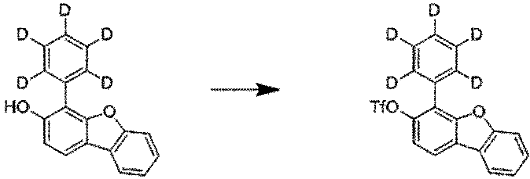
[중간체 4-b] [중간체 4-c]
상기 합성예 1-(1)에서 사용한 3-클로로-10-히드록시페난실렌 대신 [중간체 4-b]를 사용한 것을 제외하고는 동일한 방법으로 합성하여 [중간체 4-c]를 얻었다.
합성예 4-(4) : 중간체 4-d의 합성

[중간체 4-c] [중간체 4-d]
상기 합성예 2-(1)에서 사용한 3,6-디브로모디벤조퓨란 대신 브로모페닐(d5)를 페닐-d5-보론산 대신 [화학식 3-a]를 사용한 것을 제외하고는 동일한 방법으로 합성하여 [중간체 4-d]를 얻었다.
합성예
4-(5) : 중간체 4-e의 합성

[중간체 4-d] [중간체 4-e]
상기 합성예3-(1)에서 3-메톡시디벤조퓨란 대신 [중간체 4-d]를 사용한 것을 제외하고는 동일한 방법으로 합성하여 [중간체 4-e]를 얻었다.
합성예 4-(6) : 화합물 25의 합성

[중간체 4-e] [중간체 3-h] [화합물 25]
상기 합성예 1-(10)에서 사용한 [중간체 1-h] 대신 [중간체 3-h]를 [중간체 1-i] 대신 [중간체 4-e]를 사용한 것을 제외하고는 동일한 방법으로 합성하여 [화합물 25]를 얻었다.
MS (MALDI-TOF) : m/z 763.37 [M+]
합성예 5 : 화합물 1의 합성
합성예 5-(1) : 중간체 5-a의 합성

[중간체 5-a]
건조된 반응기에 질소를 채운 후 2-클로로9-히드록시페난실렌 (30g, 131mmol)와 피리딘 (31.1g, 393mmol) ,메틸렌클로라이드 300 ml 을 넣고 영도로 낮춰주었다. 그 후 트리플로로메탄설포닉언하이드라이드 (44.42g, 157 mmol)을 천천히 적가한 후 1시간 동안 교반시켰다. 반응이 종료되면 5℃ 증류수 200 ml를 천천히 적가한 후 메틸렌클로라이드와 증류수를 사용하여 추출한 뒤 메틸렌클로라이드와 헥산으로 재결정하여 [중간체 5-a](33.0g, 70%)을 얻었다.
합성예 5-(2) : 중간체 5-b의 합성

[중간체 5-a] [중간체 5-b]
250 ml 둥근바닥플라스크에 [중간체 5-a] (33 g, 91 mmol), 10-페닐(d5)-안트라센-9-보론산 (30.5 g, 101mmol), 테트라키스(트리페닐포스핀)팔라듐(2.11 g, 2mmol), 포타슘카보네이트 (25.29 g, 183mmol)을 넣고 톨루엔270 ml, 에탄올 90 ml, 물 60 ml를 넣어 반응기의 온도를 80 ℃로 승온시키고 12시간 교반하였다. 반응 종료 후 반응물을 상온으로 낮추고 메탄올을 부어 교반한 후 유기층을 분리하였다. 유기층은 감압 농축 후 톨루엔과 아세톤으로 재결정하여 [중간체 5-b] (30g, 69%)을얻었다
합성예 5-(3) : 중간체 5-c의 합성

[중간체 5-c]
1 L 둥근 바닥 플라스크에 질소분위기에서 2-브로모-1,3-디메톡시벤젠 (50 g, 230 mmol), 테트라하이드로퓨란 400ml를 넣고 녹인 후 -78 ℃까지 온도를 낮추고, 노말부틸리튬 (167 ml, 280 mmol)을 적가하였다. 동일 온도에서 2 시간을 교반한 후 트리메틸보레이트 (36 ml, 320 mmol)를 넣고 실온에서 밤새 교반하였다. 반응 완료 후 2노말 염산을 천천히 적가하여 산성화하였다. 물과 에틸아세테이트로 추출하여 유기층을 분리한 후 마그네슘설페이트로 수분을 제거하였다. 물질은 감압 농축한 후 헵탄과 톨루엔으로 재결정하여 [중간체 5-c] (20.8 g, 50%)를 얻었다.
합성예 5-(4) : 중간체 5-d의 합성

[중간체 5-c] [중간체 5-d]
500 ml 둥근바닥플라스크에 [중간체 5-a] (20.8 g, 110 mmol), 1-브로모-2-플루오로-3-아이오도벤젠 (28.7g, 95mmol), 테트라키스(트리페닐포스핀)팔라듐 (33g, 29 mmol), 탄산나트륨 (30.3 g, 290mmol)을 넣고 톨루엔 200 ml, 에탄올 60 ml, 물 60 ml를 넣었다. 반응기의 온도를 80℃로 승온시키고 12 시간 교반한 후 반응이 종료되면 반응기의 온도를 실온으로 낮추고 에틸아세테이트로 추출하고 유기층을 분리하였다. 유기층은 감압 농축 후 컬럼크로마토그래피로 분리하여 [중간체 5-d] (22.3 g, 63%)를 얻었다.
합성예 5-(5) : 중간체 5-e의 합성

[중간체 5-d] [중간체 5-e]
상기 합성예 1-(2)에서 사용한 10-페닐(d5)-안트라센-9-보론산 대신 1-나프탈렌 d7-보론산을 사용하고, [중간체 1-a] 대신 [중간체 5-d] 를 사용한 것을 제외하고는 동일한 방법으로 합성하여 [중간체 5-e](16.6g, 72%)를 얻었다.
합성예 5-(6) : 중간체 5-f의 합성

[중간체 5-e] [중간체 5-f]
500 ml 둥근바닥플라스크에 [중간체 5-e] (19 g, 52 mmol), 브롬화수소산 (48 ml, 260 mmol), 아세트산 100 ml를 넣고 12 시간 교반하였다. 반응완료 후 상온으로 식힌 후 물을 부어 교반한 후 반응물을 물과 에틸아세테이트로 추출하여 유기층을 분리하였다. 유기층은 감압농축하여 헵탄으로 재결정한 뒤 여과하고 건조하여 [중간체 5-f] (16 g, 91%)를 얻었다.
합성예 5-(7) : 중간체 5-g의 합성

[중간체 5-f] [중간체 5-g]
500 ml 둥근 바닥 플라스크에 [중간체 5-f] (16 g, 47 mmol), 포타슘 카보네이트(19.5 g, 141 mmol), N-메틸-2-피롤리돈 112 ml를 넣고 12시간 교반하였다. 반응완료 후 상온 냉각 후 물과 에틸아세테이트로 추출하여 유기층을 분리하였다. 물질은 감압농축하여 헵탄으로 재결정하여 [중간체 5-g] (13 g,86%)를 얻었다.
합성예 5-(8) : 중간체 5-h의 합성

[중간체 5-g] [중간체 5-h]
상기 합성예 1-(1) 에서 사용한 2-클로로9-히드록시페난실렌 대신 [중간체 5-g]를 사용한 것을 제외하고는 동일한 방법으로 합성하여 [중간체 5-h](15g, 81.5%)를 얻었다.
합성예 5-(9) : 중간체 5-i의 합성

[중간체 5-b] [중간체 5-i]
[중간체 5-b](30g, 64 mmol), 비스피나콜라토디보론 (21.1 g, 83 mmol), 팔라듐(II) 염화-1,1'-비스(다이페닐포스피노)페로센 (1.8g, 3mmol), 칼륨 아세테이트 (18.8g, 191mmol), 톨루엔 300 ml를 넣고 10시간 동안 환류교반 시키고 반응종료 후 고체를 걸러낸 후 여액을 감압하여 농축하였다. 메틸렌클로라이드와 헵탄으로 컬럼크로마토그래피를 하여 [중간체 5-i] (22g, 61%)를 얻었다.
합성예 5-(10) : 화합물 1의 합성

[중간체 5-h] [중간체 5-i] [화합물 1]
250 ml 둥근 바닥플라스크에 [중간체 5-h] (13g, 29mmol), [중간체 5-i](17.8 g, 32mmol), 테트라키스(트리페닐포스핀)팔라듐 (0.67 g, 0.6mmol), 포타슘카보네이트 (8 g, 58mmol)을 넣고 톨루엔91 ml, 에탄올39 ml, 물26 ml를 넣어 반응기의 온도를 80℃로 승온시키고 12시간 교반하였다. 반응 종료 후 반응물을 상온으로 낮추고 메탄올을 부어 교반한 후 유기층을 분리하였다. 유기층은 감압 농축후 톨루엔과 아세톤으로 재결정하여 [화합물 1] (7.3g, 34.3%)을 얻었다.
<도판트 제조>
[화학식 D1] 및 [화학식 D2] 중 어느 하나로 표시되는 화합물 : PCT/KR2015/004552에 기재된 실시예를 참조하여 도판트 물질을 합성하였다.
[화학식 D3] 내지 [화학식 D5] 중 어느 하나로 표시되는 화합물 : 아래 합성예 6 내지 8에 따라 제조하였다.
합성예 6: BD 2의 합성
합성예 6-(1): 중간체 6-a의 합성

<중간체 6-a>
1 L 반응기에 4-tert-butylaniline (40 g, 236 mmol)을 메틸렌클로라이드 400 mL에 녹인 후 0 ℃에서 교반한다. 그 후 N-브로모썩신이미드 (42 g, 236 mmol)을 반응기에 천천히 넣는다. 상온으로 올린 후 4 시간 동안 교반시킨다. 반응종료 후 H2O를 상온에서 적가한 후 메틸렌클로라드로 추출한다. 유기층을 농축하고 컬럼 크로마토그래피로 분리하여 <중간체 6-a> (48 g, 수율 80%)을 얻었다.
합성예 6-2. <중간체 6-b>의 합성

<중간체 6-b>
2 L 반응기에 <중간체 6-a> (80 g, 351 mmol), 물 450 mL을 넣고 교반한다. 황산 104 mL을 넣는다. 0 ℃에서 아질산나트륨 (31.5 g, 456 mmol)을 물 240 mL에 녹여 적가한다. 적가 후 0 ℃에서 2 시간 교반한다. 0 ℃에서 포타슘아이오다이드 (116.4 g, 701 mmol)을 물 450 mL에 녹여 적가한다. 적가 후 상온에서 6 시간 교반한다. 반응종료 후 상온에서 소듐티오설페이트 수용액을 넣고 교반한다. 에틸아세테이로 추출하고 유기층을 농축하고 컬럼 크로마토그래피로 분리하여 <중간체 6-b> (58 g, 수율 51%)을 얻었다.
합성예 6-3. <중간체 6-c>의 합성

<중간체 6-c>
1 L 반응기에 1-브로모-5-아이오도벤젠 (50.1 g, 177 mmol), 4-터셔리뷰틸아닐린 (58 g, 389 mmol), 팔라듐 아세테이트 (1.6 g, 7 mmol), 소듐터셔리부톡사이드 (51 g, 530 mmol), 비스(디페닐포스피노)-1,1'-바이나프틸 (4.4 g, 7 mmol), 톨루엔 500 mL를 넣고 24 시간 동안 환류 교반한다. 반응종료 후 여과하여 여액을 농축한다. 컬럼 크로마토그래피로 분리하여 <중간체 6-c> (52.8 g, 수율 80%)을 얻었다.
합성예 6-4. <중간체 6-d>의 합성

<중간체 6-d>
250 mL 반응기에 <중간체 6-c> (36.5 g, 98 mmol), 3-브로모벤조티오펜 (20.9 g, 98 mmol), 팔라듐아세테이트 (0.5 g, 2 mmol), 소듐터셔리부톡사이드 (18.9 g, 196 mmol), 트리터셔리부틸포스핀 (0.8 g, 4 mmol), 톨루엔 200 mL를 넣고 5 시간 동안 환류 교반한다. 반응종료 후 여과하여 여액을 농축하고 컬럼 크로마토그래피로 분리하여 <중간체 6-d> (35.6 g, 수율 72%)을 얻었다.
합성예 6-5. <중간체 6-e>의 합성

<중간체 6-d> <중간체 6-e>
상기 합성예 6-(4)에서 사용한 <중간체 6-c> 대신 <중간체 6-d>를 사용하고, 3-브로모벤조티오펜 대신 2-브로모-4-터셔리뷰틸-1-아이오도벤젠을 사용한 것을 제외하고는 동일한 방법으로 합성하여 <중간체 6-e>를 얻었다. (수율 67%)
합성예 6-6. BD 2의 합성

<BD 2>
300 mL 반응기에 <중간체 6-e> (16.5 g, 23 mmol), 터셔리부틸벤젠 120 mL을 넣는다. -78 ℃에서 n-부틸리튬 (42.5 mL, 68 mmol) 적가한다. 60 ℃에서 3 시간 교반한다. 동일 온도에서 질소를 불어 헵탄을 제거한다. -78 ℃에서 보론트리브로마이드 (11.3 g, 45 mmol)를 적가한 후 상온에서 1 시간 교반하고, 0 ℃에서 N,N-디아이소프로필에틸아민 (5.9 g, 45 mmol)을 적가한 후 120 ℃에서 2 시간 교반한다. 반응 종료 후 상온에서 소디움아세테이트 수용을 넣고 교반한다. 에틸아세테이트로 추출한 후 유기층을 농축하고 컬럼 크로마토그래피로 분리하여 <BD 2> (2.2 g, 수율 15%)을 얻었다.
MS (MALDI-TOF) : m/z 644.34 [M+]
합성예 7: BD 3의 합성
합성예 7-(1): 중간체 7-a의 합성

<중간체 7-a>
상기 합성예 6-(4)에서 사용한 <중간체 6-c> 대신 2,3-디메틸인돌을 사용하고, 3-브로모벤조티오펜 대신 1-브로모-2,3-디클로로벤젠을 사용한 것을 제외하고는 동일한 방법으로 합성하여 <중간체 7-a>를 얻었다. (수율 47%)
합성예 7-(2): 중간체 7-b의 합성

<중간체 7-a> <중간체 7-b>
상기 합성예 6-(4)에서 사용한 <중간체 6-c> 대신 디페닐아민을 사용하고, 3-브로모벤조티오펜 대신 <중간체 7-a>를 사용한 것을 제외하고는 동일한 방법으로 합성하여 <중간체 7-b>를 얻었다. (수율 72%)
합성예 7-(3): BD 3의 합성

<중간체 7-b> <BD 3>
상기 합성예 6-(6)에서 사용한 <중간체 5-e> 대신 <중간체 7-b>를 사용한 것을 제외하고는 동일한 방법으로 합성하여 <BD 3>를 얻었다. (수율 72%)
MS (MALDI-TOF) : m/z 369.18 [M+]
합성예 8: BD 4의 합성
합성예 8-(1): 중간체 8-a의 합성

<중간체 8-a>
상기 합성예 6-(3)에서 사용한 1-브로모-5-아이모도벤젠 대신 N -3-브로모페닐-N,N-디페닐아민을 사용하고, 4-터셔리부틸아닐린 대신 4-아미노바이페닐을 사용한 것을 제외하고는 동일한 방법으로 합성하여 <중간체 8-a>를 얻었다. (수율 55%)
합성예 8-(2): 중간체 8-b의 합성

<중간체 8-a> <중간체 8-b>
상기 합성예 6-(4)에서 사용한 <중간체 6-c> 대신 <중간체 8-a>를 사용하고, 3-브로모벤조티오펜 대신 1-브로모-2,3-디클로로벤젠을 사용한 것을 제외하고는 동일한 방법으로 합성하여 <중간체 8-b>를 얻었다. (수율 53%)
합성예
8-(3): 중간체 8-c의 합성

<중간체 8-b> <중간체 8-c>
상기 합성예 6-(4)에서 사용한 <중간체 6-c> 대신 4-페닐디페닐아민을 사용하고, 3-브로모벤조티오펜 대신 <중간체 8-b>를 사용한 것을 제외하고는 동일한 방법으로 합성하여 <중간체 8-c>를 얻었다. (수율 57%)
합성예
8-(4):
BD 4의
합성

<중간체 8-c> <BD 4>
상기 합성예 6-(6)에서 사용한 <중간체 5-e> 대신 <중간체 8-c>를 사용한 것을 제외하고는 동일한 방법으로 합성하여 <BD 4>를 얻었다. (수율 61%)
MS (MALDI-TOF) : m/z 739.32 [M+]
실시예 1 ~ 17 : 유기발광소자의 제조
ITO 글래스의 발광면적이 2mm Х 2mm 크기가 되도록 패터닝한 후 세정하였다. 상기 ITO 글래스를 진공 챔버에 장착한 후 베이스 압력이 1 Х 10-7 torr가 되도록 한 후 상기 ITO 위에 2-TNATA(400 Å), HT(200 Å) 순으로 성막한다. 이어서, 발광층으로 하기 표 1에 기재된 호스트 화합물과 도판트 화합물 3 wt%를 혼합하여 성막(250Å)한 다음, 전자 수송층으로 [화학식 E-1]을 (300 Å), 전자 주입층으로 Liq (10 Å)를 차례로 성막하고, 음극인 Al (1000 Å)을 성막하여 유기발광소자를 제작하였다. 상기 유기발광소자의 발광특성은 10 mA/cm2 에서 측정을 하였다.
[DNTPD] [HT]

[화학식 E-1] [BD 1]

[BD 2] [BD 3]

[BD 4] [BD 5] [BD 6]

비교예
1 내지
비교예
11
상기 실시예 1 내지 17에서 사용된 호스트 화합물 대신에 [BH 1] 내지 [BH 8] 화합물을 사용한 것 이외에는 동일하게 유기발광소자를 제작하였으며,
상기 유기발광 소자의 발광 특성은 10 mA/cm2 에서 측정하였으며, 얻어진 유기발광소자의 평가결과를 아래 표 1에 나타내었다.
[BH 1] [BH 2] [BH 3] [BH 4]

[BH 5] [BH 6] [BH 7] [BH 8]

[표 1]

상기 표 1에서 보는 바와 같이 본 발명에 의한 유기발광 화합물을 호스트 물질로서 포함하는 유기발광소자는 비교예 1 내지 11에 따른 화합물을 호스트 물질로 사용하는 유기발광소자에 비하여 보다 장수명 및 고효율 특성을 가지는 것으로 나타남을 알 수 있어, 유기발광 소자로서 응용가능성 높은 것을 나타내고 있다.
본 발명에 따른 상기 안트라센 유도체는 발광층내 호스트로서 사용되는 경우에, 기존 물질에 비하여 보다 장수명 및 고효율의 특성을 가지고 있어, 유기발광소자에 적용하는 경우에 개선된 특성을 나타내어 유기발광소자 및 이와 관련한 산업 분야에서 산업상 이용가능성이 높다.
Claims (17)
- 하기 [화학식 A]로 표시되는 유기발광 화합물.[화학식 A]
 상기 [화학식 A]에서,상기 치환기 R1 내지 R8은 각각 동일하거나 상이하고, 서로 독립적으로 수소 또는 중수소이며,상기 치환기 Ar1 및 Ar2는 각각 동일하거나 상이하고, 서로 독립적으로 적어도 일부가 중수소 치환 또는 비치환된 탄소수 6 내지 50의 아릴기, 또는 적어도 일부가 중수소 치환 또는 비치환된 탄소수 1 내지 30의 알킬기이며,상기 n 은 0~3의 정수이고, n이 2이상인 경우에 각각의 Ar1은 각각 동일하거나 상이하고,상기 m는 0~4의 정수이되, m이 2이상인 경우에 각각의 Ar2은 각각 동일하거나 상이하고,n + m은 0이 아니며,상기 디벤조퓨란기내 각각의 방향족고리의 탄소원자가 상기 Ar1 또는 Ar2 와 결합되지 않는 경우에 이들은 각각 수소 또는 중수소가 결합되며,L1은 하기 구조식 B로 표시되는 연결기이며,[구조식 B]
 상기 구조식 B에서,상기 치환기 R11 내지 R20 중에서 두 개의 치환기는 각각 상기 화학식 A로 표시되는 화합물내 안트라세닐기와 연결되거나, 또는 상기 화학식 A로 표시되는 화합물내 디벤조퓨란기와 연결되는 단일결합이고,상기 치환기 R11 내지 R20 중에서 단일결합이 아닌 나머지 8개의 치환기는 각각 동일하거나 상이하고, 서로 독립적으로 수소, 중수소, 치환 또는 비치환된 탄소수 1 내지 30의 알킬기, 치환 또는 비치환된 탄소수 2 내지 30의 알케닐기, 치환 또는 비치환된 탄소수 2 내지 30의 알키닐기, 치환 또는 비치환된 탄소수 3 내지 30의 시클로알킬기, 치환 또는 비치환된 탄소수 5 내지 30의 시클로알케닐기, 치환 또는 비치환된 탄소수 1 내지 30의 알콕시기, 치환 또는 비치환된 탄소수 6 내지 30의 아릴옥시기, 치환 또는 비치환된 탄소수 1 내지 30의 알킬티옥시기, 치환 또는 비치환된 탄소수 5 내지 30의 아릴티옥시기, 치환 또는 비치환된 탄소수 1 내지 30의 알킬아민기, 치환 또는 비치환된 탄소수 5 내지 30의 아릴아민기, 치환 또는 비치환된 탄소수 6 내지 50의 아릴기, 치환 또는 비치환되고 이종 원자로 O, N 또는 S를 갖는 탄소수 2 내지 50의 헤테로아릴기, 시아노기, 니트로기, 할로겐기, 치환 또는 비치환된 탄소수 1 내지 30의 알킬실릴기, 치환 또는 비치환된 탄소수 6 내지 30의 아릴실릴기 중에서 선택되는 어느 하나이고,여기서, 상기 [화학식 A] 및 [구조식 B]에서의 상기 '치환 또는 비치환된'에서의 '치환'은 중수소, 시아노기, 할로겐기, 니트로기, 탄소수 1 내지 24의 알킬기, 탄소수 3 내지 24의 시클로알킬기, 탄소수 1 내지 24의 할로겐화된 알킬기, 탄소수 6 내지 24의 아릴기, 탄소수 7 내지 24의 아릴알킬기, 탄소수 2 내지 24의 헤테로아릴기, 탄소수 1 내지 24의 알콕시기, 탄소수 1 내지 24의 알킬실릴기, 탄소수 6 내지 24의 아릴실릴기, 탄소수 6 내지 24의 아릴옥시기로 이루어진 군에서 선택된 1개 이상의 치환기로 치환되는 것을 의미한다.
 - 제 1 항에 있어서,상기 n은 0 이고, 상기 m은 1 또는 2 이거나,상기 n은 1 또는 2 이고, 상기 m은 0 인 것을 특징으로 하는 유기발광 화합물.
- 제 1 항에 있어서,상기 치환기 Ar1 및 Ar2는 각각 동일하거나 상이하고, 서로 독립적으로 적어도 일부가 중수소 치환된 탄소수 6 내지 50의 아릴기인 것을 특징으로 하는 유기발광 화합물.
- 제 3 항에 있어서,상기 치환기 Ar1 및 Ar2는 각각 동일하거나 상이하고, 서로 독립적으로 적어도 일부가 중수소 치환된 탄소수 6 내지 20의 아릴기인 것을 특징으로 하는 유기발광 화합물.
- 제 4 항에 있어서,상기 치환기 Ar1 및 Ar2는 각각 동일하거나 상이하고, 서로 독립적으로 적어도 일부가 중수소 치환된 페닐기, 적어도 일부가 중수소 치환된 나프틸기, 적어도 일부가 중수소 치환된 페난트레닐기 및 적어도 일부가 중수소 치환된 비페닐기 중에서 선택되는 어느 하나인 것을 특징으로 하는 유기발광 화합물.
- 제 1 항에 있어서,상기 치환기 R11 내지 R20 중에서 단일결합이 아닌 나머지 8개의 치환기는 각각 동일하거나 상이하고, 서로 독립적으로 수소 또는 중수소인 것을 특징으로 하는 유기발광 화합물.
- 제 1 항에 있어서,상기 화학식 A로 표시되는 화합물에서,상기 안트라세닐기 또는 디벤조퓨란기와 결합되는 구조식 B내 두 개의 단일결합은 각각 치환기 R11, R14, R15, R17 및 R18 중에서 선택되는 것을 특징으로 하는 유기발광 화합물
- 제 7 항에 있어서,상기 화학식 A로 표시되는 화합물에서,상기 안트라세닐기 또는 디벤조퓨란기와 결합되는 구조식 B내 두 개의 단일결합은 각각 치환기 R11, R14 및 R18 중에서 선택되는 두 개의 치환기;이거나,또는, 치환기 R11 및 R17 중에서 선택;되는 것을 특징으로 하는 유기발광 화합물
- 제 7항에 있어서,치환기 R11는 상기 화학식 A로 표시되는 화합물내 안트라세닐기와 연결되는 단일결합이고,상기 치환기 R14 및 R18 중에서 선택되는 하나의 치환기는 상기 화학식 A로 표시되는 화합물내 디벤조퓨란기와 연결되는 단일결합인 것을 특징으로 하는 유기발광 화합물.
- 제 1 항에 있어서,상기 화학식 A로 표시되는 화합물은 하기 [화학식 A-1] 또는 [화학식 A-2]로 표시되는 것을 특징으로 하는 유기발광 화합물.[화학식 A-1] [화학식 A-2]
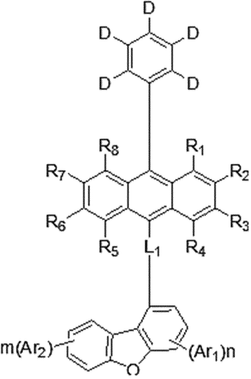
 상기 R1 내지 R8, L1, Ar1, Ar2, m 및 n은 제1항에서 정의한 바와 동일하다.
 - 제 1 항에 있어서,상기 화학식 A로 표시되는 유도체 화합물이 하기 <화합물 1> 내지 <화합물 35> 중 어느 하나로 표시되는 유기발광 화합물.
 <화합물 1><화합물 2><화합물 3><화합물 4>
 <화합물 5><화합물 6><화합물 7><화합물 8>
 <화합물 9><화합물 10><화합물 11><화합물 12>
 <화합물 13><화합물 14><화합물 15><화합물 16>
 <화합물 17><화합물 18><화합물 19><화합물 20>
 <화합물 21><화합물 22><화합물 23><화합물 24>
 <화합물 25><화합물 26><화합물 27><화합물 28>
 <화합물 29><화합물 30><화합물 31><화합물 32>
 <화합물 33><화합물 34><화합물 35>
 - 제1전극;상기 제1전극에 대향된 제2전극; 및상기 제1전극과 상기 제2전극 사이에 개재된 유기층;을 포함하고, 상기 유기층이 제1항 내지 제11항 중 어느 한 항의 유기발광 화합물을 1종 이상 포함하는 것을 특징으로 하는 유기 발광 소자.
- 제 12 항에 있어서,상기 유기발광소자내 유기층은 정공 주입층, 정공 수송층, 정공 주입 기능 및 정공 수송 기능을 동시에 갖는 기능층, 발광층, 전자 수송층, 및 전자 주입층 중 적어도 하나를 포함하는 것을 특징으로 하는 유기 발광 소자.
- 제 13 항에 있어서,상기 유기발광소자내 상기 제1전극과 상기 제2전극 사이에 개재된 유기층이 발광층을 포함하며,상기 발광층은 호스트와 도판트로 이루어지고, 상기 유기발광 화합물이 호스트로서 사용되는 것을 특징으로 하는 유기 발광소자.
- 제 13 항에 있어서,상기 각각의 층중에서 선택된 하나 이상의 층은 증착공정 또는 용액공정에 의해 형성되는 것을 특징으로 하는 유기 발광 소자.
- 제 12 항에 있어서,상기 유기발광소자는 평판 디스플레이 장치; 플렉시블 디스플레이 장치; 단색 또는 백색의 평판 조명용 장치; 및, 단색 또는 백색의 플렉시블 조명용 장치;에서 선택되는 어느 하나의 장치에 사용되는 것을 특징으로 하는 유기 발광 소자.
- 제 14 항에 있어서,상기 도판트는 하기 [화학식 D1] 내지 [화학식 D7] 중 어느 하나로 표시되는 화합물을 적어도 1종 사용되는 것을 특징으로 하는 유기 발광 소자.[화학식 D1]
 [화학식 D2]
 상기 [화학식 D1] 및 [화학식 D2]에서, A31, A32, E1 및 F1은 각각 동일하거나 상이하고, 서로 독립적으로 치환 또는 비치환된 탄소수 6 내지 50의 방향족 탄화수소 고리, 또는 치환 또는 비치환된 탄소수 2 내지 40의 방향족 헤테로고리이고;상기 A31의 방향족 고리내 서로 이웃한 두 개의 탄소원자와, 상기 A32의 방향족 고리내 서로 이웃한 두개의 탄소원자는 상기 치환기 R51 및 R52에 연결된 탄소원자와 5원환을 형성함으로써 각각 축합고리를 형성하며;상기 연결기 L21 내지 L32는 각각 동일하거나 상이하고, 서로 독립적으로 단일 결합, 치환 또는 비치환된 탄소수 1 내지 60의 알킬렌기, 치환 또는 비치환된 탄소수 2 내지 60의 알케닐렌기, 치환 또는 비치환된 탄소수 2 내지 60의 알키닐렌기, 치환 또는 비치환된 탄소수 3 내지 60의 시클로알킬렌기, 치환 또는 비치환된 탄소수 2 내지 60의 헤테로시클로알킬렌기, 치환 또는 비치환된 탄소수 6 내지 60의 아릴렌기 또는 치환 또는 비치환된 탄소수 2 내지 60의 헤테로아릴렌기 중에서 선택되며;상기 W는 N-R53, CR54R55, SiR56R57, GeR58R59, O, S, Se 중에서 선택되는 어느 하나이며;상기 치환기 R51 내지 R59, Ar21 내지 Ar28은 각각 동일하거나 상이하고, 서로 독립적으로 수소, 중수소, 치환 또는 비치환된 탄소수 1 내지 30의 알킬기, 치환 또는 비치환된 탄소수 6 내지 50의 아릴기, 치환 또는 비치환된 탄소수 2 내지 30의 알케닐기, 치환 또는 비치환된 탄소수 2 내지 20의 알키닐기, 치환 또는 비치환된 탄소수 3 내지 30의 시클로알킬기, 치환 또는 비치환된 탄소수 5 내지 30의 시클로알케닐기, 치환 또는 비치환된 탄소수 2 내지 50의 헤테로아릴기, 치환 또는 비치환된 탄소수 2 내지 30의 헤테로시클로알킬기, 치환 또는 비치환된 탄소수 1 내지 30의 알콕시기, 치환 또는 비치환된 탄소수 6 내지 30의 아릴옥시기, 치환 또는 비치환된 탄소수 1 내지 30의 알킬티옥시기, 치환 또는 비치환된 탄소수 5 내지 30의 아릴티옥시기, 치환 또는 비치환된 탄소수 1 내지 30의 알킬아민기, 치환 또는 비치환된 탄소수 5 내지 30의 아릴아민기, 치환 또는 비치환된 탄소수 1 내지 30의 알킬실릴기, 치환 또는 비치환된 탄소수 5 내지 30의 아릴실릴기, 치환 또는 비치환된 탄소수 1 내지 30의 알킬게르마늄기, 치환 또는 비치환된 탄소수 1 내지 30 의 아릴게르마늄기 시아노기, 니트로기, 할로겐기 중에서 선택되는 어느 하나이되,상기 R51 및 R52는 서로 연결되어 지환족, 방향족의 단일환 또는 다환 고리를 형성할 수 있으며, 상기 형성된 지환족, 방향족의 단일환 또는 다환 고리의 탄소원자는 N, O, P, Si, S, Ge, Se, Te 중에서 선택되는어느 하나 이상의 헤테로원자로 치환될 수 있으며;상기 p11 내지 p14, r11 내지 r14 및 s11 내지 s14는 각각 1 내지 3의 정수이되, 이들 각각이 2 이상인 경우에 각각의 연결기 L21 내지 L32는 서로 동일하거나 상이하고,상기 x1은 1 또는 2의 정수이고, y1 및 z1은 각각 동일하거나 상이하며, 서로 독립적으로 0 내지 3의 정수이며,상기 Ar21 과 Ar22, Ar23과 Ar24, Ar25와 Ar26 및 Ar27과 Ar28은 각각 서로 연결되어 고리를 형성할 수 있고;상기 화학식 D1에서 A32고리내 서로 이웃한 두개의 탄소원자는 상기 구조식 Q11의 *와 결합하여 축합고리를 형성하고,상기 화학식 D2에서 상기 A31고리내 서로 이웃한 두개의 탄소원자는 상기 구조식 Q12의 *와 결합하여 축합고리를 형성하고, 상기 A32 고리내 서로 이웃한 두개의 탄소원자는 상기 구조식 Q11의 *와 결합하여 축합고리를 형성할 수 있다.[화학식 D3]
 상기 [화학식 D3] 에서,상기 X1는 B, P, P=O 중에서 선택되는 어느 하나이고상기 T1 내지 T3은 각각 서로 동일하거나 상이하고, 서로 독립적으로 치환 또는 비치환된 탄소수 6 내지 50의 방향족 탄화수소 고리, 또는 치환 또는 비치환된 탄소수 2 내지 40의 방향족 헤테로고리이고;상기 Y1는 N-R61, CR62R63, O, S, SiR64R65 중에서 선택되는 어느 하나이며;상기 Y2는 N-R66, CR66R68, O, S, SiR69R70 중에서 선택되는 어느 하나이며;상기 R61 내지 R70은 각각 서로 동일하거나 상이하고, 서로 독립적으로 수소, 중수소, 치환 또는 비치환된 탄소수 1 내지 30의 알킬기, 치환 또는 비치환된 탄소수 6 내지 50의 아릴기, 치환 또는 비치환된 탄소수 3 내지 30의 시클로알킬기, 치환 또는 비치환된 탄소수 2 내지 50의 헤테로아릴기, 치환 또는 비치환된 탄소수 1 내지 30의 알콕시기, 치환 또는 비치환된 탄소수 6 내지 30의 아릴옥시기, 치환 또는 비치환된 탄소수 1 내지 30의 알킬티옥시기, 치환 또는 비치환된 탄소수 5 내지 30의 아릴티옥시기, 치환 또는 비치환된 탄소수 1 내지 30의 알킬아민기, 치환 또는 비치환된 탄소수 5 내지 30의 아릴아민기, 치환 또는 비치환된 탄소수 1 내지 30의 알킬실릴기, 치환 또는 비치환된 탄소수 5 내지 30의 아릴실릴기, 시아노기, 할로겐기 중에서 선택되는 어느 하나이며, 상기 R61 내지 R70은 각각 상기 T1 내지 T3중에서 선택되는 하나 이상의 고리와 결합하여 지환족 또는 방향족의 단일환 또는 다환고리를 추가적으로 형성할 수 있다.[화학식 D4] [화학식 D5]
 상기 [화학식 D4] 및 [화학식 D5]에서,상기 X2는 B, P, P=O 중에서 선택되는 어느 하나이고상기 T4 내지 T6는 [화학식 D3]에서 T1 내지 T3와 동일하며,상기 Y4 내지 Y6는 [화학식 D3]에서 Y1 내지 Y2 와 동일하며,[화학식 D6] [화학식 D7]
 상기 X3는 B, P, P=O 중에서 선택되는 어느 하나이고상기 T7 내지 T9는 [화학식 D3]에서 T1 내지 T3와 동일하며,상기 Y6는 [화학식 D3]에서 Y1 내지 Y2와 동일하며,상기 치환기 R71 내지 R72은 각각 서로 동일하거나 상이하고, 서로 독립적으로 수소, 중수소, 치환 또는 비치환된 탄소수 1 내지 30의 알킬기, 치환 또는 비치환된 탄소수 6 내지 50의 아릴기, 치환 또는 비치환된 탄소수 3 내지 30의 시클로알킬기, 치환 또는 비치환된 탄소수 2 내지 50의 헤테로아릴기, 치환 또는 비치환된 탄소수 1 내지 30의 알콕시기, 치환 또는 비치환된 탄소수 6 내지 30의 아릴옥시기, 치환 또는 비치환된 탄소수 1 내지 30의 알킬티옥시기, 치환 또는 비치환된 탄소수 5 내지 30의 아릴티옥시기, 치환 또는 비치환된 탄소수 1 내지 30의 알킬아민기, 치환 또는 비치환된 탄소수 5 내지 30의 아릴아민기, 치환 또는 비치환된 탄소수 1 내지 30의 알킬실릴기, 치환 또는 비치환된 탄소수 5 내지 30의 아릴실릴기, 니트로기, 시아노기, 할로겐기 중에서 선택되는 어느 하나이며, 상기 R71 및 R72는 각각 서로 연결되어 지환족 또는 방향족의 단일환 또는 다환고리를 추가적으로 형성하거나 또는 상기 Q1 고리 또는 Q3 고리와 결합하여 지환족 또는 방향족의 단일환 또는 다환고리를 추가적으로 형성할 수 있고.여기서, 상기 [화학식 D1] 내지 [화학식 D7]에서의 상기'치환 또는 비치환된'에서의 '치환'은 중수소, 시아노기, 할로겐기, 히드록시기, 니트로기, 탄소수 1 내지 24의 알킬기, 탄소수 1 내지 24의 할로겐화된 알킬기, 탄소수 2 내지 24의 알케닐기, 탄소수2 내지 24의 알키닐기, 탄소수 1 내지 24의 헤테로알킬기, 탄소수 6 내지 24의 아릴기, 탄소수7 내지 24의 아릴알킬기, 탄소수 2 내지 24의 헤테로아릴기 또는 탄소수 2 내지 24의 헤테로아릴알킬기, 탄소수 1 내지 24의 알콕시기, 탄소수 1 내지 24의 알킬아미노기, 탄소수6 내지 24의 아릴아미노기, 탄소수 1 내지 24의 헤테로 아릴아미노기, 탄소수 1 내지 24의 알킬실릴기, 탄소수6 내지 24의 아릴실릴기, 탄소수6 내지 24의 아릴옥시기로 이루어진 군에서 선택된 1개 이상의 치환기로 치환되는 것을 의미한다.
Priority Applications (4)
| Application Number | Priority Date | Filing Date | Title |
|---|---|---|---|
| JP2021564513A JP7266713B2 (ja) | 2019-06-10 | 2020-05-21 | 有機発光素子用化合物及びこれを含む有機発光素子 |
| EP20823636.4A EP3981855A4 (en) | 2019-06-10 | 2020-05-21 | COMPOUND FOR ORGANIC LIGHT EMITTING ELEMENT AND ORGANIC LIGHT EMITTING ELEMENT THEREOF |
| US17/607,019 US20220216431A1 (en) | 2019-06-10 | 2020-05-21 | Compound for organic light-emitting diode and organic light-emitting diode comprising same |
| CN202080031701.5A CN113748106B (zh) | 2019-06-10 | 2020-05-21 | 有机发光元件用化合物及包括该化合物的有机发光元件 |
Applications Claiming Priority (2)
| Application Number | Priority Date | Filing Date | Title |
|---|---|---|---|
| KR20190068201 | 2019-06-10 | ||
| KR10-2019-0068201 | 2019-06-10 |
Publications (1)
| Publication Number | Publication Date |
|---|---|
| WO2020251183A1 true WO2020251183A1 (ko) | 2020-12-17 |
Family
ID=73429590
Family Applications (1)
| Application Number | Title | Priority Date | Filing Date |
|---|---|---|---|
| PCT/KR2020/006654 WO2020251183A1 (ko) | 2019-06-10 | 2020-05-21 | 유기발광 소자용 화합물 및 이를 포함하는 유기발광소자 |
Country Status (6)
| Country | Link |
|---|---|
| US (1) | US20220216431A1 (ko) |
| EP (1) | EP3981855A4 (ko) |
| JP (1) | JP7266713B2 (ko) |
| KR (1) | KR102176164B1 (ko) |
| CN (1) | CN113748106B (ko) |
| WO (1) | WO2020251183A1 (ko) |
Cited By (1)
| Publication number | Priority date | Publication date | Assignee | Title |
|---|---|---|---|---|
| CN113603665A (zh) * | 2021-07-30 | 2021-11-05 | 上海传勤新材料有限公司 | 一种含有二苯并杂环取代菲和蒽的有机电子材料及其应用 |
Families Citing this family (5)
| Publication number | Priority date | Publication date | Assignee | Title |
|---|---|---|---|---|
| US20200395553A1 (en) * | 2019-06-12 | 2020-12-17 | Sfc Co., Ltd. | Organic electroluminescent device |
| KR20220126245A (ko) * | 2021-03-08 | 2022-09-15 | 에스에프씨 주식회사 | 유기발광 화합물 및 이를 포함하는 유기발광소자 |
| WO2022191583A1 (ko) * | 2021-03-08 | 2022-09-15 | 에스에프씨 주식회사 | 유기발광소자 |
| WO2022215527A1 (ja) * | 2021-04-06 | 2022-10-13 | 出光興産株式会社 | 化合物及び有機エレクトロルミネッセンス素子 |
| KR20230100986A (ko) * | 2021-12-29 | 2023-07-06 | 에스에프씨 주식회사 | 유기발광소자 |
Citations (7)
| Publication number | Priority date | Publication date | Assignee | Title |
|---|---|---|---|---|
| WO2009069537A1 (ja) * | 2007-11-30 | 2009-06-04 | Toray Industries, Inc. | 発光素子材料および発光素子 |
| KR20090086015A (ko) | 2008-02-05 | 2009-08-10 | 에스에프씨 주식회사 | 안트라센 유도체 및 이를 포함하는 유기전계발광소자 |
| KR101111406B1 (ko) | 2011-06-22 | 2012-04-12 | 덕산하이메탈(주) | 유기전기소자, 유기전기소자용 신규 화합물 및 조성물 |
| KR20170009714A (ko) * | 2015-07-14 | 2017-01-25 | 에스에프씨 주식회사 | 고효율의 유기 발광 소자 |
| KR20170044001A (ko) * | 2015-10-13 | 2017-04-24 | 에스에프씨 주식회사 | 저계조 영역에서의 휘도감소율이 개선된 유기 발광 소자 |
| KR20180007906A (ko) * | 2016-07-14 | 2018-01-24 | 에스에프씨 주식회사 | 고효율 특성을 갖는 유기 발광 소자 |
| KR20180077887A (ko) * | 2016-12-29 | 2018-07-09 | 에스에프씨 주식회사 | 고효율을 갖는 유기 발광 소자 |
Family Cites Families (5)
| Publication number | Priority date | Publication date | Assignee | Title |
|---|---|---|---|---|
| KR102201097B1 (ko) * | 2015-01-20 | 2021-01-11 | 에스에프씨주식회사 | 유기발광소자용 화합물 및 이를 포함하는 유기 발광 소자 |
| KR102342339B1 (ko) * | 2015-03-18 | 2021-12-22 | 에스에프씨주식회사 | 유기발광소자용 화합물 및 이를 포함하는 유기 발광 소자 |
| US20160351817A1 (en) * | 2015-05-27 | 2016-12-01 | Samsung Display Co., Ltd. | Organic light-emitting device |
| CN106467554A (zh) * | 2016-07-29 | 2017-03-01 | 江苏三月光电科技有限公司 | 一种含硼有机电致发光化合物及其应用 |
| CN108409761A (zh) * | 2018-02-07 | 2018-08-17 | 瑞声科技(南京)有限公司 | 一种有机发光材料及其应用 |
-
2020
- 2020-05-21 CN CN202080031701.5A patent/CN113748106B/zh active Active
- 2020-05-21 WO PCT/KR2020/006654 patent/WO2020251183A1/ko unknown
- 2020-05-21 KR KR1020200061106A patent/KR102176164B1/ko active IP Right Grant
- 2020-05-21 JP JP2021564513A patent/JP7266713B2/ja active Active
- 2020-05-21 EP EP20823636.4A patent/EP3981855A4/en active Pending
- 2020-05-21 US US17/607,019 patent/US20220216431A1/en active Pending
Patent Citations (7)
| Publication number | Priority date | Publication date | Assignee | Title |
|---|---|---|---|---|
| WO2009069537A1 (ja) * | 2007-11-30 | 2009-06-04 | Toray Industries, Inc. | 発光素子材料および発光素子 |
| KR20090086015A (ko) | 2008-02-05 | 2009-08-10 | 에스에프씨 주식회사 | 안트라센 유도체 및 이를 포함하는 유기전계발광소자 |
| KR101111406B1 (ko) | 2011-06-22 | 2012-04-12 | 덕산하이메탈(주) | 유기전기소자, 유기전기소자용 신규 화합물 및 조성물 |
| KR20170009714A (ko) * | 2015-07-14 | 2017-01-25 | 에스에프씨 주식회사 | 고효율의 유기 발광 소자 |
| KR20170044001A (ko) * | 2015-10-13 | 2017-04-24 | 에스에프씨 주식회사 | 저계조 영역에서의 휘도감소율이 개선된 유기 발광 소자 |
| KR20180007906A (ko) * | 2016-07-14 | 2018-01-24 | 에스에프씨 주식회사 | 고효율 특성을 갖는 유기 발광 소자 |
| KR20180077887A (ko) * | 2016-12-29 | 2018-07-09 | 에스에프씨 주식회사 | 고효율을 갖는 유기 발광 소자 |
Non-Patent Citations (1)
| Title |
|---|
| See also references of EP3981855A4 |
Cited By (1)
| Publication number | Priority date | Publication date | Assignee | Title |
|---|---|---|---|---|
| CN113603665A (zh) * | 2021-07-30 | 2021-11-05 | 上海传勤新材料有限公司 | 一种含有二苯并杂环取代菲和蒽的有机电子材料及其应用 |
Also Published As
| Publication number | Publication date |
|---|---|
| CN113748106B (zh) | 2024-01-02 |
| KR102176164B1 (ko) | 2020-11-09 |
| JP7266713B2 (ja) | 2023-04-28 |
| CN113748106A (zh) | 2021-12-03 |
| JP2022530265A (ja) | 2022-06-28 |
| EP3981855A4 (en) | 2023-04-12 |
| EP3981855A1 (en) | 2022-04-13 |
| US20220216431A1 (en) | 2022-07-07 |
Similar Documents
| Publication | Publication Date | Title |
|---|---|---|
| WO2018066830A1 (ko) | 장수명, 저전압 및 고효율 특성을 갖는 유기 발광 소자 | |
| WO2018066831A1 (ko) | 장수명, 저전압 및 고효율 특성을 갖는 유기 발광 소자 | |
| WO2013081315A1 (ko) | 유기전기소자용 화합물, 이를 포함하는 유기전기소자 및 그 전자 장치 | |
| WO2017082556A1 (ko) | 신규한 유기발광 화합물 및 이를 포함하는 유기 발광 소자 | |
| WO2017023021A1 (ko) | 고효율을 갖는 유기 발광 소자 | |
| WO2020105990A1 (ko) | 신규한 보론 화합물 및 이를 포함하는 유기발광소자 | |
| WO2020251183A1 (ko) | 유기발광 소자용 화합물 및 이를 포함하는 유기발광소자 | |
| WO2015174682A1 (ko) | 방향족아민기를 포함하는 헤테로고리 화합물및 이를 포함하는 유기 발광 소자 | |
| WO2013105747A1 (ko) | 유기전기 소자용 화합물, 이를 이용한 유기전기소자 및 그 전자 장치 | |
| WO2016126022A1 (ko) | 저전압구동이 가능하며 장수명을 갖는 유기 발광 소자 | |
| WO2016171429A2 (ko) | 유기 발광 소자용 화합물 및 이를 포함하는 유기발광소자 | |
| WO2016108419A1 (ko) | 고효율과 장수명을 갖는 유기 발광 소자 | |
| WO2016200080A1 (ko) | 고효율을 갖는 유기 발광 소자 | |
| WO2017010726A1 (ko) | 유기전기 소자용 화합물을 이용한 유기전기소자 및 그 전자 장치 | |
| WO2021112403A1 (ko) | 유기화합물을 포함하는 유기전기소자 및 이를 포함하는 전자 장치 | |
| WO2013122364A2 (ko) | 유기전기소자용 화합물, 이를 포함하는 유기전기소자 및 그 전자 장치 | |
| WO2021010770A1 (ko) | 신규한 보론 화합물 및 이를 포함하는 유기발광소자 | |
| WO2015190867A2 (ko) | 유기전기 소자용 화합물, 이를 이용한 유기전기소자 및 그 전자 장치 | |
| WO2017010749A1 (ko) | 고효율의 유기 발광 소자 | |
| WO2013108997A1 (ko) | 유기전기소자용 화합물, 이를 포함하는 유기전기소자 및 그 전자 장치 | |
| WO2016167505A1 (ko) | 신규한 헤테로고리 화합물 및 이를 포함하는 유기 발광 소자 | |
| WO2013069939A1 (ko) | 유기전기소자용 화합물, 이를 포함하는 유기전기소자 및 그 전자 장치 | |
| WO2021096228A1 (ko) | 유기 발광 소자 | |
| WO2020153650A1 (ko) | 유기 발광 소자용 화합물 및 이를 포함하는 장수명의 유기발광소자 | |
| WO2011145876A2 (ko) | 신규 하이브리드 유기 화합물 및 이를 이용한 유기 전계 발광소자 |
Legal Events
| Date | Code | Title | Description |
|---|---|---|---|
| 121 | Ep: the epo has been informed by wipo that ep was designated in this application |
Ref document number: 20823636 Country of ref document: EP Kind code of ref document: A1 |
|
| ENP | Entry into the national phase |
Ref document number: 2021564513 Country of ref document: JP Kind code of ref document: A |
|
| NENP | Non-entry into the national phase |
Ref country code: DE |
|
| ENP | Entry into the national phase |
Ref document number: 2020823636 Country of ref document: EP Effective date: 20220110 |