WO2020250978A1 - 放射線検出装置及び放射線撮影システム - Google Patents
放射線検出装置及び放射線撮影システム Download PDFInfo
- Publication number
- WO2020250978A1 WO2020250978A1 PCT/JP2020/023029 JP2020023029W WO2020250978A1 WO 2020250978 A1 WO2020250978 A1 WO 2020250978A1 JP 2020023029 W JP2020023029 W JP 2020023029W WO 2020250978 A1 WO2020250978 A1 WO 2020250978A1
- Authority
- WO
- WIPO (PCT)
- Prior art keywords
- radiation
- scintillator
- detection device
- photoelectric conversion
- radiation detection
- Prior art date
- Legal status (The legal status is an assumption and is not a legal conclusion. Google has not performed a legal analysis and makes no representation as to the accuracy of the status listed.)
- Ceased
Links
Images



Classifications
-
- A—HUMAN NECESSITIES
- A61—MEDICAL OR VETERINARY SCIENCE; HYGIENE
- A61B—DIAGNOSIS; SURGERY; IDENTIFICATION
- A61B6/00—Apparatus or devices for radiation diagnosis; Apparatus or devices for radiation diagnosis combined with radiation therapy equipment
-
- G—PHYSICS
- G01—MEASURING; TESTING
- G01T—MEASUREMENT OF NUCLEAR OR X-RADIATION
- G01T1/00—Measuring X-radiation, gamma radiation, corpuscular radiation, or cosmic radiation
- G01T1/16—Measuring radiation intensity
- G01T1/20—Measuring radiation intensity with scintillation detectors
-
- G—PHYSICS
- G01—MEASURING; TESTING
- G01T—MEASUREMENT OF NUCLEAR OR X-RADIATION
- G01T1/00—Measuring X-radiation, gamma radiation, corpuscular radiation, or cosmic radiation
- G01T1/16—Measuring radiation intensity
- G01T1/20—Measuring radiation intensity with scintillation detectors
- G01T1/202—Measuring radiation intensity with scintillation detectors the detector being a crystal
Definitions
- the present invention relates to a radiation detection device that detects incident radiation and a radiography system including the radiation detection device.
- radiography is performed by moving a patient to a radiation room equipped with a radiography device (radiation imaging system) including a radiation detection device, or portable radiation for patients who cannot be carried to the radiation room.
- a radiography device radiography imaging system
- Many photographs have been proposed, such as photographs using an imaging device.
- the radiography apparatus is composed of a radiation generator (radiation tube), a high-voltage generator, a battery, etc. in addition to the radiation detection apparatus, and a plurality of radiographic apparatus together with an imaging plate using a film cassette or a brilliant fluorescent plate. It can be carried and used in the hospital room.
- Patent Document 1 and Patent Document 2 describe a device provided with two radiation panels as a radiation detection device for energy subtraction imaging by a one-shot method (single exposure method).
- Patent Document 1 and Patent Document 2 describe a radiation detection device including two radiation panels.
- a filter, a mounting substrate electrically connected to the two radiation panels, and the like may be laminated.
- the radiation detection apparatus described in Patent Document 1 and Patent Document 2 has a problem that the apparatus becomes thick because it is simply a configuration in which two radiation panels are laminated.
- the radiation detection apparatus described in Patent Document 1 and Patent Document 2 is configured to simply stack two radiation panels, there is a wide gap around the scintillator included in the radiation panel, and this wide gap There is also a problem that the device is vulnerable to a load and lacks robustness depending on the part.
- One embodiment of the present invention has been made in view of such a problem, and in a radiation detection device provided with two radiation panels, a mechanism for suppressing thickening and improving robustness is provided.
- the purpose is to provide.
- the radiation detection device includes a first scintillator that converts incident radiation into light and a first photoelectric conversion unit that converts the light from the first scintillator into an electric signal.
- a first radiation panel including a first sensor substrate, a second scintillator that converts the radiation incident through the first radiation panel into light, and the light from the second scintillator.
- the first sensor substrate comprises a second sensor substrate including a second photoelectric conversion unit for converting light into an electric signal, and a second radiation panel including the first photoelectric conversion unit.
- the substrate has recesses where t1 ⁇ t2, and the second scintillator is a substrate. At least a part of the region is housed in the recess.
- another embodiment of the present invention includes a radiography system including the above-mentioned radiation detection device.
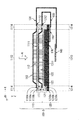
- FIG. 5 is a schematic view of the radiation detection device according to the first embodiment of the present invention as viewed from the side where radiation is incident. It is a figure which shows an example of the internal structure in the II cross section of FIG. 1 in the radiation detection apparatus which concerns on 1st Embodiment of this invention. It is a figure which shows an example of the internal structure in the II cross section of FIG. 1 in the radiation detection apparatus which concerns on a comparative example. It is a figure which shows an example of the internal structure in the II cross section of FIG. 1 in the radiation detection apparatus which concerns on 2nd Embodiment of this invention. It is a figure which shows an example of the internal structure in the II cross section of FIG. 1 in the radiation detection apparatus which concerns on 3rd Embodiment of this invention. It is a figure which shows the 4th Embodiment of this invention, and shows an example of the schematic structure of the radiography system including the radiation detection apparatus 100 which concerns on any one of 1st to 3rd Embodiment.
- the radiation is typically X-rays, but the present invention is not limited to these X-rays, for example, ⁇ rays and ⁇ rays. It may be a line, a ⁇ -ray, or the like.
- FIG. 1 is a schematic view of the radiation detection device 100 according to the first embodiment of the present invention as viewed from the side where radiation is incident.
- a first sensor substrate 111 and a first protective layer 113 included in the first radiation panel are arranged on the side where the radiation of the radiation detection device 100 is incident.
- FIG. 1 shows a first connection wiring portion 130 that is electrically connected to the first sensor substrate 111.
- the incident direction of radiation is the Z-axis direction
- the first surface 1110a which is a biaxial direction orthogonal to the Z-axis direction and is the radiation incident surface of the first sensor substrate 111, is orthogonal to each other.
- the XYZ coordinate system is shown in which the two axial directions are the X-axis direction and the Y-axis direction.
- FIG. 2 is a diagram showing an example of an internal configuration in the II cross section of FIG. 1 in the radiation detection device 100 according to the first embodiment of the present invention.
- the XYZ coordinate system corresponding to the XYZ coordinate system shown in FIG. 1 is illustrated, and the incident direction of the radiation R is shown by a white arrow.
- the same reference numerals are given to the configurations similar to those shown in FIG.
- the radiation detection device 100 according to the first embodiment shown in FIG. 2 will be referred to as “radiation detection device 100-1”.
- the radiation detection device 100-1 includes a first radiation panel 110, a second radiation panel 120, a first connection wiring portion 130, and a first mounting substrate 140. , A second connection wiring portion 150, and a second mounting board 160 are included. As shown in FIG. 2, the radiation detection device 100-1 is configured by laminating a first radiation panel 110 and a second radiation panel 120.
- the first radiation panel 110 includes a first sensor substrate 111, a first scintillator 112, and a first protective layer 113.
- the first sensor substrate 111 includes a first photoelectric conversion unit 1111 arranged on a first surface 1110a, which is a radiation incident surface on which radiation R is incident, and a first connection pad unit 1112.
- FIG. 2 illustrates an embodiment in which the first photoelectric conversion unit 1111 is arranged inside the first sensor substrate 111, but the present embodiment is not limited to this embodiment, and the first The embodiment arranged on the upper part of the sensor substrate 111 of the above is also applicable to the present embodiment.
- the first photoelectric conversion unit 1111 is a component unit that converts the light from the first scintillator 112 into a radiographic image signal which is an electric signal.
- the first photoelectric conversion unit 1111 is formed, for example, by arranging a plurality of pixels two-dimensionally in the X-axis direction and the Y-axis direction. Further, each pixel of the first photoelectric conversion unit 1111 may include a photoelectric conversion element that converts light into an electric charge and a switching element for outputting an electric signal corresponding to the electric charge generated by the photoelectric conversion element.
- a first connection wiring portion 130 such as a flexible cable for connecting the first sensor board 111 to the first mounting board 140 is connected to the first connection pad portion 1112. Since the first connection pad portion 1112 is arranged by, for example, crimping the first connection wiring portion 130 by heating and pressurizing, specifically, the substrate peripheral region 1114 including the first connection pad portion 1112. Is preferably at least 0.30 mm or more.
- the first sensor substrate 111 includes a first photoelectric conversion unit 1111 on a second surface 1110b opposite to the first surface 1110a (specifically, the first photoelectric conversion unit 1111 and its structure).
- a first photoelectric conversion unit 1111 on a second surface 1110b opposite to the first surface 1110a (specifically, the first photoelectric conversion unit 1111 and its structure).
- the thickness t1 of the substrate central region 1113 of the first sensor substrate 111 corresponds to the length in the Z-axis direction of the substrate central region 1113 of the first sensor substrate 111.
- the thickness t2 of the substrate peripheral region 1114 of the first sensor substrate 111 corresponds to the length in the Z-axis direction of the substrate peripheral region 1114 of the first sensor substrate 111. That is, due to the difference between the thickness t2 of the substrate peripheral region 1114 of the first sensor substrate 111 and the thickness t1 of the substrate central region 1113 of the first sensor substrate 111, the recess 1110c in the substrate central region 1113 of the first sensor substrate 111 Is formed.
- the first scintillator 112 is a component that converts the radiation R incident through the first protective layer 113 into light.
- the light converted by the first scintillator 112 is incident on the first photoelectric conversion unit 1111.
- the first scintillator 112 is arranged on the side where the radiation R is incident in the first photoelectric conversion unit 1111.
- the first protective layer 113 can function as an electromagnetic shield or a reflective layer in addition to the function of protecting the first scintillator 112.
- the light converted by the first scintillator 112 can be reflected by the first protective layer 113.
- the first scintillator 112 and the first protective layer 113 may form a first wavelength conversion unit.
- the second radiation panel 120 includes a second sensor substrate 121, a second scintillator 122, and a second protective layer 123.
- the second sensor substrate 121 includes a second photoelectric conversion unit 1211 arranged on the first surface 1210a, which is a radiation incident surface on which the radiation R is incident, and a second connection pad unit 1212.
- FIG. 2 illustrates an embodiment in which the second photoelectric conversion unit 1211 is arranged inside the second sensor substrate 121, but the present embodiment is not limited to this embodiment, and the second is not limited to this embodiment.
- the embodiment arranged on the upper part of the sensor substrate 121 of the above is also applicable to the present embodiment.
- the second photoelectric conversion unit 1211 is a component unit that converts the light from the second scintillator 122 into a radiographic image signal which is an electric signal.
- the second photoelectric conversion unit 1211 is formed, for example, by arranging a plurality of pixels in a two-dimensional manner in the X-axis direction and the Y-axis direction. Further, each pixel of the second photoelectric conversion unit 1211 may include a photoelectric conversion element that converts light into an electric charge and a switching element for outputting an electric signal corresponding to the electric charge generated by the photoelectric conversion element.
- a second connection wiring section 150 such as a flexible cable for connecting the second sensor board 121 to the second mounting board 160 is connected to the second connection pad section 1212. Further, in FIG. 2, in the second sensor substrate 121, the surface opposite to the first surface 1210a is shown as the second surface 1210b.
- the second scintillator 122 is a component that converts the radiation R incident through the first radiation panel 110 into light.
- the light converted by the second scintillator 122 is incident on the second photoelectric conversion unit 1211.
- the second scintillator 122 is arranged on the side where the radiation R is incident in the second photoelectric conversion unit 1211.
- the second protective layer 123 can function as an electromagnetic shield or a reflective layer in addition to the function of protecting the second scintillator 122.
- the light converted by the second scintillator 122 can be reflected by the second protective layer 123.
- the second scintillator 122 and the second protective layer 123 can form a second wavelength conversion unit.
- the first connection wiring unit 130 is a connection wiring unit such as a flexible cable for electrically connecting the first sensor board 111 and the first mounting board 140.
- the first mounting board 140 is, for example, a mounting board that transmits and receives various signals to and from the first sensor board 111 via the first connection wiring unit 130.
- the second connection wiring unit 150 is a connection wiring unit such as a flexible cable for electrically connecting the second sensor board 121 and the second mounting board 160.
- the second mounting board 160 is, for example, a mounting board that transmits and receives various signals to and from the second sensor board 121 via the second connection wiring unit 150.
- the material of the first sensor substrate 111 and the second sensor substrate 121 may be a transparent insulating substrate such as a glass substrate.
- the first radiation panel 110 and the second radiation panel 120 have a sensor protection layer (not shown) that protects the first photoelectric conversion unit 1111 and the second photoelectric conversion unit 1211, respectively. ) Can be further included.
- the sensor protection layer is arranged so as to cover the first photoelectric conversion unit 1111 and the second photoelectric conversion unit 1211, respectively.
- the sensor protection layer may be composed of, for example, SiN, TiO 2 , LiF, Al 2 O 3 or MgO.
- the sensor protective layer may be, for example, a polyphenylene sulfide resin, a fluororesin, a polyether ether ketone resin, a liquid crystal polymer, a polyether nitrile resin, a polysulfone resin, a polyether sulfone resin, a polyarylate resin, a polyamideimide resin, or a polyetherimide. It may be composed of a resin, a polyimide resin, an epoxy resin or a silicone resin.
- the sensor protection layer is made of a material having a high transmittance for the wavelength of the light converted by the first scintillator 112 so that the light converted by the first scintillator 112 can pass through.
- the first scintillator 112 and the second scintillator 122 are arranged corresponding to the regions of the first photoelectric conversion unit 1111 and the second photoelectric conversion unit 1211, respectively, and for example, a phosphor having columnar crystals and particles.
- a phosphor having a crystalline crystal is used.
- a scintillator made of a phosphor having a columnar crystal light generated by the phosphor propagates in the columnar crystal, so that light scattering is small and a high-resolution radiographic image can be obtained.
- a material for a scintillator composed of a phosphor having columnar crystals a material containing an alkali halide as a main component is preferably used.
- CsI: Tl CsI: Na, CsBr: Tl, NaI: Tl, LiI: Eu. , KI: Tl and the like are used.
- the production method can be formed by simultaneously depositing CsI (cesium iodide) and TlI.
- a scintillator made of a phosphor having particulate crystals contains a plurality of scintillator particles that convert radiation into light and a binder that fixes the plurality of scintillator particles to each other, and can be easily formed by coating or the like. An inexpensive phosphor layer can be obtained.
- the scintillator particles have metallic acid sulfurization represented by the general formula Me 2 O 2 S: Re from the viewpoints of moisture resistance, luminous efficiency, thermal process resistance, and afterglow. It is preferably composed of objects.
- Me is any one of La, Y, and Gd
- Re is at least one of Tb, Sm, Eu, Ce, Pr, and Tm.
- the binder is composed of, for example, a resin.
- the binder is preferably one that dissolves in an organic solvent and has thixotropic properties.
- it is preferably composed of a cellulosic resin such as ethyl cellulose or nitrocellulose, an acrylic resin such as polymethyl methacrylate, or a polyvinyl acetal resin such as polyvinyl butyral solvent grade.
- the binder may be composed of a combination of two or more kinds of these resins. Then, the scintillator particles and the binder are added to the organic solvent that dissolves the binder. This forms a paste.
- the scintillator made of a phosphor having particulate crystals may be formed by directly applying the paste to the sensor substrate, or may be formed into a sheet shape in another step and then formed into a sheet shape via an adhesive. It may be formed by laminating with.
- the first protective layer 113 protects the first scintillator 112 and can also function as an electromagnetic shield or a reflective layer.
- the light converted by the first scintillator 112 can be reflected by the first protective layer 113.
- the first protective layer 113 may be composed of, for example, a metal foil or a metal thin film.
- the thickness of the first protective layer 113 is preferably 1 ⁇ m or more and 100 ⁇ m or less. This is because if the thickness of the first protective layer 113 is thinner than 1 m, pinhole defects are likely to occur when the first protective layer 113 is formed, and the light-shielding property is inferior.
- the thickness of the first protective layer 113 exceeds 100 ⁇ m, the amount of radiation R absorbed becomes too large, and the step formed by the first protective layer 113 becomes too large.
- the material of the first protective layer 113 include metal materials such as aluminum, gold, silver, copper, and aluminum alloys.
- a desired resin layer such as PET can be arranged on the outermost layer in order to improve scratch resistance on the metal material layer.
- a resin layer such as a sheet having adhesiveness can be arranged on the forming side of the first scintillator 112. This resin layer is used as an adhesive material or a hot melt material for bonding the first scintillator 112, the first sensor substrate 111, and the first protective layer 113.
- the second radiation panel 120 can use the same material as the first radiation panel 110. Further, FIG. 2 shows an example in which the first sensor substrate 111 in which the recess 1110c is formed and the second sensor substrate 121 in which the recess is not formed are used, but both are the sensor substrate 111 in which the recess is formed. And 121 may be used.
- FIG. 3 is a diagram showing an example of the internal configuration in the II cross section of FIG. 1 in the radiation detection device 200 according to the comparative example.
- the XYZ coordinate system corresponding to the XYZ coordinate system shown in FIG. 1 is illustrated, and the incident direction of the radiation R is shown by a white arrow.
- the radiation detection device 200 has a first radiation panel 210, a second radiation panel 220, a first connection wiring portion 230, a first mounting board 240, and a second connection. It is configured to have a wiring portion 250 and a second mounting board 260. As shown in FIG. 3, the radiation detection device 200 is configured by laminating a first radiation panel 210 and a second radiation panel 220.
- the first radiation panel 210 includes a first sensor substrate 211, a first scintillator 212, and a first protective layer 213.
- the first sensor substrate 211 includes a first photoelectric conversion unit 2111 formed on a first surface 2110a, which is a radiation incident surface on which radiation R is incident, and a first connection pad unit 2112. .
- the first photoelectric conversion unit 2111 is a configuration unit that converts the light from the first scintillator 212 into a radiographic image signal which is an electric signal.
- a first connection wiring section 230 for connecting the first sensor board 211 to the first mounting board 240 is connected to the first connection pad section 2112.
- the first sensor substrate 211 is not provided with a recess on the second surface 2110b on the side opposite to the first surface 2110a. It is different from the radiation detection device 100-1 according to the embodiment of.
- the first scintillator 212 and the first protective layer 213 shown in FIG. 3 have a configuration corresponding to the first scintillator 112 and the first protective layer 113 shown in FIG. 2, respectively.
- the second radiation panel 220 includes a second sensor substrate 221, a second scintillator 222, and a second protective layer 223.
- the second radiation panel 220 shown in FIG. 3 has a configuration corresponding to the second radiation panel 120 shown in FIG.
- first connection wiring section 230 and the first mounting board 240 shown in FIG. 3 have a configuration corresponding to the first connection wiring section 130 and the first mounting board 140 shown in FIG. 2, respectively.
- second connection wiring section 250 and the second mounting board 260 shown in FIG. 3 have a configuration corresponding to the second connection wiring section 150 and the second mounting board 160 shown in FIG. 2, respectively.
- the radiation detection device 100-1 according to the first embodiment shown in FIG. 2 and the radiation detection device 200 according to the comparative example shown in FIG. 3 are compared.
- the second surface 2110b of the first sensor substrate 211 is not provided with a recess
- the recess 1110c is provided on the second surface 1110b of the first sensor substrate 111. Since the radiation detection device 100-1 according to the first embodiment shown in FIG. 2 is provided with the recess 1110c, the second scintillator 122 of the second radiation panel 120 is provided in the recess 1110c at least.
- the second scintillator 122 of the second radiation panel 120 is arranged in the recess 1110c so as to accommodate a part of the region in the thickness direction of the first sensor substrate 111. More specifically, in the radiation detection device 100-1 according to the first embodiment shown in FIG. 2, in the laminated structure of the first radiation panel 110 and the second radiation panel 120, the second scintillator 122 is formed in the recess 1110c. A second wavelength conversion unit including the second protective layer 123 and the second protective layer 123 are arranged and configured to be fitted. According to the configuration of the first embodiment shown in FIG.
- the radiation detection device is arranged so that at least a part of the region of the second scintillator 122 is accommodated in the recess 1110c of the first sensor substrate 111.
- the thickness of 100-1 (length in the Z-axis direction) can be reduced.
- the gap portion around the second scintillator 122 can be made smaller, and as a result, the load bearing capacity of the radiation detection device 100-1 is enhanced. Can be done. That is, according to the radiation detection device 100-1 according to the first embodiment shown in FIG. 2, it is possible to suppress the thickening and improve the robustness.
- the bottom surface of the recess 1110c in the substrate central region 1113 of the first sensor substrate 111 is second. It can be bonded to the radiation panel 120 of No. 1 with a resin or the like. Further, in the present embodiment, the bottom surface of the recess 1110c in the first radiation panel 110 is not only bonded to the second radiation panel 120, but is also formed between the recess 1110c to be fitted and the second radiation panel 120. The gaps can be filled with resin. With these configurations, the rigidity and robustness of the radiation detection device 100-1 can be further improved.
- a first photoelectric conversion unit 1111 that receives light from the first scintillator 112 and a first connection pad unit 1112 are formed.
- the first sensor substrate 111 was manufactured. At this time, the thickness of the first sensor substrate 111 was set to 0.5 mm.
- a slightly adhesive resin film was transferred to the region of the first sensor substrate 111 where the first photoelectric conversion unit 1111 was formed for the purpose of protection from etching. Further, in order to form the bottom surface of the recess 1110c on the second surface 1110b of the first sensor substrate 111, a slightly adhesive resin is similarly formed on the region other than the recess forming region on the second surface 1110b of the first sensor substrate 111. The film was transferred.
- the first sensor substrate 111 was immersed in a 10% hydrofluoric acid solution.
- the immersion time at this time is determined by, for example, a pre-calculated etching rate, and etching is performed to a desired thickness.
- etching of 400 ⁇ m was performed to obtain about 100 ⁇ m as the thickness t1 of the substrate central region 1113 in which the recess 1110c of the first sensor substrate 111 was formed.
- the first sensor substrate 111 is sufficiently rinsed with pure water. Subsequently, the resin films attached to both sides of the first sensor substrate 111 were peeled off to obtain a first sensor substrate 111 having recesses 1110c. Further, a protective layer material made of polyimide was applied to the first photoelectric conversion unit 1111 and cured at 200 degrees for 2 hours to form a sensor protective layer (not shown).
- the first protective layer 113 in which the sheet adhesive layer was arranged on the film-like sheet in which the moisture-proof protective layer made of Al was laminated on the layer made of PET was bonded so as to cover the entire first scintillator 112. ..
- a vacuum laminator was used, a laminated sheet was placed and held at 0.4 Pa, 90 ° C. for 5 minutes, the entire first scintillator 112 was covered with the first protective layer 113, and , The peripheral end of the first protective layer 113 was adhered to the first sensor substrate 111 so as to be in full peripheral contact with the adhesive sheet.
- the first connection wiring portion 130 was thermocompression bonded to the first connection pad portion 1112 provided on the first sensor substrate 111.
- a first radiation panel 110 electrically connected to the first mounting board 140 via the first connection wiring unit 130 was obtained.
- the second sensor substrate 121 was manufactured in the same manner as the first sensor substrate 111, except that the recess was not formed in the second sensor substrate 121.
- the second scintillator 122 and the second protective layer 123 are formed on the first surface 1210a of the second sensor substrate 121 by the same steps as the first scintillator 112 and the first protective layer 113 described above. did.
- the second connection wiring portion 150 was thermocompression bonded to the second connection pad portion 1212 provided on the second sensor substrate 121.
- a second radiation panel 120 electrically connected to the second mounting board 160 via the second connection wiring unit 150 was obtained.
- the first radiation panel 110 and the second radiation panel 120 were bonded together. Specifically, epoxy resin is applied to the recess 1110c and the flat surface of the second surface 1110b of the first sensor substrate 111, and the second scintillator 122 and the second protective layer 123 of the second radiation panel 120 are recessed. Both panels were overlapped and laminated so as to fit into 1110c.
- the radiation detection device 100-1 according to the first embodiment was obtained in which the gap between the recess 1110c of the first sensor substrate 111 and the second radiation panel 120 was filled with epoxy resin. ..
- the radiation detection device 200 according to the comparative example shown in FIG. 3 was also manufactured.
- the radiation detection device 100-1 according to the first embodiment manufactured through the above steps It was produced by the same process as the second radiation panel 120. After that, the produced first radiation panel 210 and the second radiation panel 220 were superposed on each other to produce a radiation detection device 200 according to a comparative example.
- the radiation detection device 100-1 according to the first embodiment produced in the above-described embodiment has a thinner thickness (length in the Z-axis direction) than the radiation detection device 200 according to the comparative example, and also relates to the comparative example.
- the load bearing capacity on the device panel surface was better than that of the radiation detection device 200. That is, according to the embodiment of the first embodiment, it was found that the radiation detection device 100-1 according to the first embodiment can suppress the thickening and improve the robustness.
- the schematic view of the radiation detection device according to the second embodiment seen from the side where the radiation is incident is the schematic view seen from the side where the radiation is incident in the radiation detection device 100 according to the first embodiment shown in FIG. The same is true.
- FIG. 4 is a diagram showing an example of an internal configuration in the I-I cross section of FIG. 1 in the radiation detection device 100 according to the second embodiment of the present invention.
- the XYZ coordinate system corresponding to the XYZ coordinate system shown in FIG. 1 is illustrated, and the incident direction of the radiation R is shown by a white arrow.
- the same reference numerals are given to the configurations similar to those shown in FIGS. 1 and 2, and detailed description thereof will be omitted.
- the radiation detection device 100 according to the second embodiment shown in FIG. 4 will be referred to as “radiation detection device 100-2”.
- the radiation detection device 100-2 has a first radiation panel 110, a second radiation panel 120, a first connection wiring portion 130, and a first mounting substrate 140. , A second connection wiring unit 150, and a second mounting board 160. As shown in FIG. 4, the radiation detection device 100-2 is configured by laminating a first radiation panel 110 and a second radiation panel 120.
- the first sensor substrate 111 includes the first photoelectric conversion unit 1111 on the second surface 1110b (specifically, the first photoelectric conversion unit 1111 and one of its outer periphery).
- the thickness of the substrate central region 1113 (including the portion) is t1
- the thickness of the substrate peripheral region 1114 not including the first photoelectric conversion portion 1111 (including the first connection pad portion 1112) is t2
- the thickness of the second scintillator 122 When the thickness is t3, the following equation (2) t2-t1> t3 ... (2) A recess 1110c that satisfies the condition is provided.
- the bottom surface of the recess 1110c in the substrate central region 1113 of the first sensor substrate 111 is second. It can be bonded to the radiation panel 120 of No. 1 with a resin or the like. Since the radiation detection device 100-2 according to the second embodiment shown in FIG. 4 is provided with the recess 1110c satisfying the equation (2), the second scintillator 122 of the second radiation panel 120 has the recess. The 1110c is arranged so that the entire region is accommodated in the thickness direction of the first sensor substrate 111. As shown in FIG.
- the first sensor substrate 111 is provided with moisture-proof protection of the second scintillator 122. It can also serve as rigidity protection.
- the second connection pad portion 1212 and the second connection wiring portion of the second radiation panel 120 are formed on the bonding surface between the first sensor board 111 and the second sensor board 121. Moisture resistance can be further improved by arranging so as not to contain 150. Further, in the present embodiment, after the recess 1110c of the first sensor substrate 111 and the second radiation panel 120 are fitted, the gap remaining in the recess 1110c can be filled with an appropriate resin or the like.
- a metal reflective layer is provided in the recess 1110c of the first sensor substrate 111, or the recess is provided.
- a resin in which reflective particles such as titanium oxide are contained in the resin to be filled in 1110c can be used.
- the first radiation panel 110 is subjected to the same steps as the above-described embodiment of the radiation detection device 100-1 according to the first embodiment.
- a second scintillator 122 was formed on the second sensor substrate 121 with a thickness of 300 ⁇ m to obtain a second radiation panel 120.
- the first radiation panel 110 and the second radiation panel 120 were bonded together. Specifically, both radiation panels are arranged so that the second scintillator 122 is fitted in the recess 1110c of the first sensor board 111, and the flat surface portion and the second surface 1110b of the second surface 1110b of the first sensor board 111 are arranged. The portion of the sensor substrate 121 in contact with the first surface 1210a of No. 2 was bonded with an epoxy resin. The second scintillator 122 is arranged so as to be surrounded by the recess 1110c of the first sensor substrate 111, so that the moisture resistance and rigidity are improved.
- the radiation detection device 100-2 according to the second embodiment was obtained.
- the radiation detection device 100-2 according to the second embodiment produced in the above-described embodiment has a thinner thickness (length in the Z-axis direction) than the radiation detection device 200 according to the comparative example, and also relates to the comparative example.
- the load bearing capacity on the device panel surface was better than that of the radiation detection device 200. That is, according to the embodiment of the second embodiment, it was found that the radiation detection device 100-2 according to the second embodiment can suppress the thickening and improve the robustness.
- FIG. 5 is a diagram showing an example of the internal configuration in the II cross section of FIG. 1 in the radiation detection device 100 according to the third embodiment of the present invention.
- the XYZ coordinate system corresponding to the XYZ coordinate system shown in FIG. 1 is illustrated, and the incident direction of the radiation R is shown by a white arrow.
- the same components as those shown in FIGS. 1, 2 and 4 are designated by the same reference numerals, and detailed description thereof will be omitted.
- the radiation detection device 100 according to the third embodiment shown in FIG. 5 will be referred to as “radiation detection device 100-3”.
- the radiation detection device 100-3 has a first radiation panel 110, a second radiation panel 120, a first connection wiring portion 130, and a first mounting substrate 140. , A second connection wiring unit 150, a second mounting board 160, and a scattered radiation prevention member 170. As shown in FIG. 5, the radiation detection device 100-3 is configured by laminating a first radiation panel 110 and a second radiation panel 120, and a second radiation panel 120 and a scattering ray prevention member 170. ing.
- the second sensor substrate 121 of the second radiation panel 120 A recess 1210c is also formed on the second surface 1210b in the above.
- the second sensor substrate 121 includes the second photoelectric conversion unit 1211 on the second surface 1210b (specifically, the second photoelectric conversion unit 1211 and a part of the outer periphery thereof.
- a recess 1210c that satisfies the condition is provided. Further, in the radiation detection device 100-3 according to the third embodiment, as shown in FIG. 5, scattered radiation based on the radiation R is generated in the recess 1210c in the second sensor substrate 121 of the second radiation panel 120. A scattered radiation prevention member 170 is arranged to prevent the radiation.
- the recesses 1110c and 1210c are formed with reference to the regions of the photoelectric conversion units 1111 and 1211. Therefore, by superimposing the recesses 1110c and 1210c of both the two sensor substrates 111 and 121, the radiographic images can be superposed more accurately.
- the scattering ray prevention member 170 is arranged in the recess 1210c of the second sensor substrate 121 as shown in FIG. As a result, it is possible to acquire a radiographic image with improved S / N while suppressing the thickening of the apparatus.
- the scattering ray prevention member 170 is arranged in the recess 1210c of the second sensor substrate 121 as shown in FIG.
- the recess 1210c when radiation R is incident from the sensor substrate surface, by arranging a grid or a filter in the recess 1210c, it is possible to acquire a radiation image with improved S / N while suppressing
- the first radiation panel 110 and the second radiation panel 120 were bonded together by the same step as in the example of the radiation detection device 100-1 according to the first embodiment described above.
- a convex radiation R scattering ray prevention member 170 is formed so as to fill the recess 1210c in the second sensor substrate 121 of the second radiation panel 120, and the radiation detection device according to the third embodiment is formed. I got 100-3.
- the radiation detection device 100-3 according to the third embodiment produced in the above-described embodiment has a thinner thickness (length in the Z-axis direction) than the radiation detection device 200 according to the comparative example, and also relates to the comparative example.
- the load bearing capacity on the device panel surface was better than that of the radiation detection device 200. That is, according to the embodiment of the third embodiment, it was found that the radiation detection device 100-3 according to the third embodiment can suppress the thickening and improve the robustness. Further, in the radiation detection device 100-3 according to the third embodiment, since the scattered radiation prevention member 170 is provided, the influence of the scattered radiation of the radiation R can be reduced, so that a radiation image having a good S / N can be obtained. I was able to do it. Further, as shown in FIG. 5, by using the sensor substrates 111 and 121 in which the same recesses 1110c and 1210c are formed, the alignment of the layers is facilitated.
- the fourth embodiment is a form in which the radiation detection device 100 according to the first to third embodiments described above is applied to a part of a radiography system.
- FIG. 6 shows a fourth embodiment of the present invention and shows an example of a schematic configuration of a radiography system including a radiation detection device 100 according to any one of the first to third embodiments. Is.
- the radiation detection device 100 shown in FIG. 6 is the radiation detection device 100 according to any one of the first to third embodiments described above.
- a radiation room for example, an X-ray room
- a control room are configured with, for example, a radiation detection device 100, a radiation generator 6050, an image generation device 6070, and a display 6080.
- the radiation generator 6050 is a device that generates radiation R (for example, X-rays).
- the image generation device 6070 includes a radiation image signal which is an electric signal obtained by the first photoelectric conversion unit 1111 of the radiation detection device 100 and a radiation image signal which is an electric signal obtained by the second photoelectric conversion unit 1211. It is a device that generates an image related to radiation R by using and.
- the image generator 6070 is configured to include a signal processing unit including an image processor and the like.
- the radiation R (for example, X-ray) generated by the radiation generator 6050 passes through the chest 6061 of the subject 6060 such as a patient and is incident on the radiation detection device 100.
- the incident radiation R (for example, X-ray) contains information on the inside of the body of the subject 6060.
- the radiation detection device 100 obtains a radiation image signal which is electrical information corresponding to the incident radiation R.
- the energy distribution of the radiation R incident on the radiation detection device 100 will be roughly classified into two energy components, a low energy component and a high energy component, for description.
- the transmittance becomes higher as the radiation R has a higher energy component. Therefore, first, the low energy component of the radiation R is absorbed by the first scintillator 112, which becomes light. Will be converted. Then, the light generated by the first scintillator 112 is converted into a radiographic image signal which is an electric signal by the first photoelectric conversion unit 1111. That is, the first photoelectric conversion unit 1111 mainly acquires a radiation image signal related to the radiation R having a low energy component.
- the high-energy component radiation R that has passed through the first scintillator 112 without being absorbed by the first scintillator 112 has passed through the first radiation panel 110 and is incident on the second scintillator 122.
- the incident high-energy component radiation R is absorbed and converted into light.
- the light generated by the second scintillator 122 is converted into a radiographic image signal which is an electric signal by the second photoelectric conversion unit 1211. That is, the second photoelectric conversion unit 1211 mainly acquires a radiation image signal related to the radiation R having a high energy component.
- the radiation image signal related to the low-energy component radiation R acquired by the first photoelectric conversion unit 1111 and the radiation image signal related to the high-energy component radiation R acquired by the second photoelectric conversion unit 1211 are After being converted into a digital signal in the image generator 6070, various signal processes are performed.
- the image generator 6070 obtains the radiation image signal related to the radiation R of the low energy component acquired by the first photoelectric conversion unit 1111 and the second photoelectric conversion unit 1211 as one of the signal processing.
- Energy subtraction processing is performed using the radiation image signal related to the radiation R of the high energy component, and an energy subtraction image is generated.
- the image related to the radiation R generated by the image generation device 6070 (for example, the energy subtraction image described above) can be displayed as an inspection result on the display 6080 (display unit) of the control room (control room). Further, the image related to the radiation R generated by the image generator 6070 can be transferred to a remote location by a network 6090 (transmission processing means) such as a telephone, a LAN, or the Internet. As a result, the image related to the radiation R generated by the image generator 6070 can be displayed as an inspection result on the display 6081 at another place such as a doctor's room, and a doctor at a remote place can make a diagnosis. Further, the image and the inspection result related to the radiation R can be stored on, for example, an optical disk or the like, or can be recorded on a recording medium such as a film 6110 by the film processor 6100.
- a recording medium such as a film 6110 by the film processor 6100.
- X-rays are used as the radiation R, and a 20 mm Al filter for removing soft X-rays is set between the radiation detection device 100 and the radiation generator 6050.
- the distance between the radiation detection device 100 and the radiation generator 6050 was adjusted to 130 cm, and the radiation detection device 100 was connected to the electric drive system.
- the radiation generator 6050 bombarded the X-ray pulse three times as radiation R at a tube voltage of 80 kV, a tube current of 250 mA, and 50 ms, and the radiation detection device 100 acquired a radiation image signal.
- the first photoelectric conversion unit 1111 and the second photoelectric conversion unit 1211 of the radiation detection device 100 have acquired two radiation image signals having different energy components. Then, the image generator 6070 generated an energy subtraction image by using two radiation image signals having different energy components.
Landscapes
- Health & Medical Sciences (AREA)
- Life Sciences & Earth Sciences (AREA)
- High Energy & Nuclear Physics (AREA)
- Molecular Biology (AREA)
- Physics & Mathematics (AREA)
- Engineering & Computer Science (AREA)
- General Physics & Mathematics (AREA)
- Spectroscopy & Molecular Physics (AREA)
- Medical Informatics (AREA)
- Nuclear Medicine, Radiotherapy & Molecular Imaging (AREA)
- Biomedical Technology (AREA)
- Crystallography & Structural Chemistry (AREA)
- Chemical & Material Sciences (AREA)
- Optics & Photonics (AREA)
- Pathology (AREA)
- Radiology & Medical Imaging (AREA)
- Biophysics (AREA)
- Heart & Thoracic Surgery (AREA)
- Surgery (AREA)
- Animal Behavior & Ethology (AREA)
- General Health & Medical Sciences (AREA)
- Public Health (AREA)
- Veterinary Medicine (AREA)
- Measurement Of Radiation (AREA)
- Apparatus For Radiation Diagnosis (AREA)
Applications Claiming Priority (2)
| Application Number | Priority Date | Filing Date | Title |
|---|---|---|---|
| JP2019-111274 | 2019-06-14 | ||
| JP2019111274A JP7196020B2 (ja) | 2019-06-14 | 2019-06-14 | 放射線検出装置及び放射線撮影システム |
Publications (1)
| Publication Number | Publication Date |
|---|---|
| WO2020250978A1 true WO2020250978A1 (ja) | 2020-12-17 |
Family
ID=73781464
Family Applications (1)
| Application Number | Title | Priority Date | Filing Date |
|---|---|---|---|
| PCT/JP2020/023029 Ceased WO2020250978A1 (ja) | 2019-06-14 | 2020-06-11 | 放射線検出装置及び放射線撮影システム |
Country Status (2)
| Country | Link |
|---|---|
| JP (1) | JP7196020B2 (https=) |
| WO (1) | WO2020250978A1 (https=) |
Cited By (1)
| Publication number | Priority date | Publication date | Assignee | Title |
|---|---|---|---|---|
| CN116735631A (zh) * | 2023-08-09 | 2023-09-12 | 同源微(北京)半导体技术有限公司 | 一种x射线成像检测单元、模块和装置 |
Citations (4)
| Publication number | Priority date | Publication date | Assignee | Title |
|---|---|---|---|---|
| US9698193B1 (en) * | 2016-09-15 | 2017-07-04 | Ka Imaging Inc. | Multi-sensor pixel architecture for use in a digital imaging system |
| JP2018107343A (ja) * | 2016-12-27 | 2018-07-05 | キヤノン株式会社 | 放射線撮像装置、その製造方法および撮像システム |
| JP2018529083A (ja) * | 2015-08-07 | 2018-10-04 | コーニンクレッカ フィリップス エヌ ヴェKoninklijke Philips N.V. | 量子ドットに基づくイメージング検出器 |
| JP2019086482A (ja) * | 2017-11-10 | 2019-06-06 | キヤノン株式会社 | 放射線撮像装置および放射線撮像システム |
-
2019
- 2019-06-14 JP JP2019111274A patent/JP7196020B2/ja active Active
-
2020
- 2020-06-11 WO PCT/JP2020/023029 patent/WO2020250978A1/ja not_active Ceased
Patent Citations (4)
| Publication number | Priority date | Publication date | Assignee | Title |
|---|---|---|---|---|
| JP2018529083A (ja) * | 2015-08-07 | 2018-10-04 | コーニンクレッカ フィリップス エヌ ヴェKoninklijke Philips N.V. | 量子ドットに基づくイメージング検出器 |
| US9698193B1 (en) * | 2016-09-15 | 2017-07-04 | Ka Imaging Inc. | Multi-sensor pixel architecture for use in a digital imaging system |
| JP2018107343A (ja) * | 2016-12-27 | 2018-07-05 | キヤノン株式会社 | 放射線撮像装置、その製造方法および撮像システム |
| JP2019086482A (ja) * | 2017-11-10 | 2019-06-06 | キヤノン株式会社 | 放射線撮像装置および放射線撮像システム |
Cited By (2)
| Publication number | Priority date | Publication date | Assignee | Title |
|---|---|---|---|---|
| CN116735631A (zh) * | 2023-08-09 | 2023-09-12 | 同源微(北京)半导体技术有限公司 | 一种x射线成像检测单元、模块和装置 |
| CN116735631B (zh) * | 2023-08-09 | 2024-02-23 | 同源微(北京)半导体技术有限公司 | 一种x射线成像检测单元、模块和装置 |
Also Published As
| Publication number | Publication date |
|---|---|
| JP7196020B2 (ja) | 2022-12-26 |
| JP2020204488A (ja) | 2020-12-24 |
Similar Documents
| Publication | Publication Date | Title |
|---|---|---|
| TWI800619B (zh) | 放射線檢測器以及放射線圖像拍攝裝置 | |
| US8957383B2 (en) | Radiation detection apparatus and radiation detection system | |
| RU2408901C1 (ru) | Устройство для обнаружения излучения и система для обнаружения излучения | |
| US20110147602A1 (en) | Radiographic imaging apparatus, radiographic imaging system, and method of producing radiographic imaging apparatus | |
| CN113167914B (zh) | 放射线检测器、放射线图像摄影装置及制造方法 | |
| TWI799539B (zh) | 放射線檢測器以及放射線圖像拍攝裝置 | |
| JP2019023579A (ja) | シンチレータ | |
| JP2017200522A (ja) | 放射線撮像装置及び放射線撮像システム | |
| US11269087B2 (en) | Radiation imaging apparatus and radiation imaging system | |
| KR20170113264A (ko) | 방사선 검출 장치 및 방사선 촬상 시스템 | |
| JP7196020B2 (ja) | 放射線検出装置及び放射線撮影システム | |
| JP6555955B2 (ja) | 放射線検出装置及び放射線撮像システム | |
| KR102860671B1 (ko) | 신틸레이터 패널, 방사선 검출기, 신틸레이터 패널의 제조 방법 및 방사선 검출기의 제조 방법 | |
| JP2004301516A (ja) | 放射線検出装置 | |
| JP6740943B2 (ja) | 放射線変換パネルおよびタルボ撮影装置 | |
| JP2018146254A (ja) | シンチレータパネル | |
| TW201831921A (zh) | 放射線檢測器以及放射線圖像攝影裝置 | |
| WO2019097847A1 (ja) | 放射線撮像パネル、放射線撮像装置および放射線撮像システム | |
| JP2017176258A (ja) | 放射線検出装置及び放射線撮像システム | |
| JP2015111105A (ja) | 放射線検出装置および撮像システム | |
| JP6759056B2 (ja) | 放射線検出装置及び放射線撮像システム | |
| WO2020129428A1 (ja) | シンチレータプレート、放射線検出装置および放射線検出システム | |
| JP2019095241A (ja) | 放射線撮像パネル、放射線撮像装置および放射線撮像システム | |
| JP2017090340A (ja) | 放射線検出装置及びその製造方法、並びに、放射線検出システム | |
| JP2019095266A (ja) | 放射線撮像パネル、放射線撮像装置および放射線撮像システム |
Legal Events
| Date | Code | Title | Description |
|---|---|---|---|
| 121 | Ep: the epo has been informed by wipo that ep was designated in this application |
Ref document number: 20823616 Country of ref document: EP Kind code of ref document: A1 |
|
| NENP | Non-entry into the national phase |
Ref country code: DE |
|
| 122 | Ep: pct application non-entry in european phase |
Ref document number: 20823616 Country of ref document: EP Kind code of ref document: A1 |