WO2020250660A1 - 半導体装置及び半導体装置の製造方法 - Google Patents
半導体装置及び半導体装置の製造方法 Download PDFInfo
- Publication number
- WO2020250660A1 WO2020250660A1 PCT/JP2020/020634 JP2020020634W WO2020250660A1 WO 2020250660 A1 WO2020250660 A1 WO 2020250660A1 JP 2020020634 W JP2020020634 W JP 2020020634W WO 2020250660 A1 WO2020250660 A1 WO 2020250660A1
- Authority
- WO
- WIPO (PCT)
- Prior art keywords
- insulating layer
- back surface
- resin
- rewiring
- semiconductor device
- Prior art date
- Legal status (The legal status is an assumption and is not a legal conclusion. Google has not performed a legal analysis and makes no representation as to the accuracy of the status listed.)
- Ceased
Links
Images














Classifications
-
- H—ELECTRICITY
- H10—SEMICONDUCTOR DEVICES; ELECTRIC SOLID-STATE DEVICES NOT OTHERWISE PROVIDED FOR
- H10W—GENERIC PACKAGES, INTERCONNECTIONS, CONNECTORS OR OTHER CONSTRUCTIONAL DETAILS OF DEVICES COVERED BY CLASS H10
- H10W70/00—Package substrates; Interposers; Redistribution layers [RDL]
- H10W70/01—Manufacture or treatment
- H10W70/05—Manufacture or treatment of insulating or insulated package substrates, or of interposers, or of redistribution layers
- H10W70/08—Manufacture or treatment of insulating or insulated package substrates, or of interposers, or of redistribution layers by depositing layers on the chip or wafer, e.g. "chip-first" RDLs
- H10W70/09—Manufacture or treatment of insulating or insulated package substrates, or of interposers, or of redistribution layers by depositing layers on the chip or wafer, e.g. "chip-first" RDLs extending onto an encapsulation that laterally surrounds the chip or wafer, e.g. fan-out wafer level package [FOWLP] RDLs
-
- H—ELECTRICITY
- H10—SEMICONDUCTOR DEVICES; ELECTRIC SOLID-STATE DEVICES NOT OTHERWISE PROVIDED FOR
- H10W—GENERIC PACKAGES, INTERCONNECTIONS, CONNECTORS OR OTHER CONSTRUCTIONAL DETAILS OF DEVICES COVERED BY CLASS H10
- H10W70/00—Package substrates; Interposers; Redistribution layers [RDL]
- H10W70/60—Insulating or insulated package substrates; Interposers; Redistribution layers
- H10W70/62—Insulating or insulated package substrates; Interposers; Redistribution layers characterised by their interconnections
- H10W70/65—Shapes or dispositions of interconnections
- H10W70/657—Shapes or dispositions of interconnections on sidewalls or bottom surfaces of the package substrates, interposers or redistribution layers
-
- H—ELECTRICITY
- H10—SEMICONDUCTOR DEVICES; ELECTRIC SOLID-STATE DEVICES NOT OTHERWISE PROVIDED FOR
- H10W—GENERIC PACKAGES, INTERCONNECTIONS, CONNECTORS OR OTHER CONSTRUCTIONAL DETAILS OF DEVICES COVERED BY CLASS H10
- H10W72/00—Interconnections or connectors in packages
- H10W72/01—Manufacture or treatment
- H10W72/0198—Manufacture or treatment batch processes
-
- H—ELECTRICITY
- H10—SEMICONDUCTOR DEVICES; ELECTRIC SOLID-STATE DEVICES NOT OTHERWISE PROVIDED FOR
- H10W—GENERIC PACKAGES, INTERCONNECTIONS, CONNECTORS OR OTHER CONSTRUCTIONAL DETAILS OF DEVICES COVERED BY CLASS H10
- H10W74/00—Encapsulations, e.g. protective coatings
- H10W74/01—Manufacture or treatment
-
- H—ELECTRICITY
- H10—SEMICONDUCTOR DEVICES; ELECTRIC SOLID-STATE DEVICES NOT OTHERWISE PROVIDED FOR
- H10W—GENERIC PACKAGES, INTERCONNECTIONS, CONNECTORS OR OTHER CONSTRUCTIONAL DETAILS OF DEVICES COVERED BY CLASS H10
- H10W74/00—Encapsulations, e.g. protective coatings
- H10W74/01—Manufacture or treatment
- H10W74/014—Manufacture or treatment using batch processing
-
- H—ELECTRICITY
- H10—SEMICONDUCTOR DEVICES; ELECTRIC SOLID-STATE DEVICES NOT OTHERWISE PROVIDED FOR
- H10W—GENERIC PACKAGES, INTERCONNECTIONS, CONNECTORS OR OTHER CONSTRUCTIONAL DETAILS OF DEVICES COVERED BY CLASS H10
- H10W74/00—Encapsulations, e.g. protective coatings
- H10W74/10—Encapsulations, e.g. protective coatings characterised by their shape or disposition
- H10W74/111—Encapsulations, e.g. protective coatings characterised by their shape or disposition the semiconductor body being completely enclosed
-
- H—ELECTRICITY
- H10—SEMICONDUCTOR DEVICES; ELECTRIC SOLID-STATE DEVICES NOT OTHERWISE PROVIDED FOR
- H10W—GENERIC PACKAGES, INTERCONNECTIONS, CONNECTORS OR OTHER CONSTRUCTIONAL DETAILS OF DEVICES COVERED BY CLASS H10
- H10W74/00—Encapsulations, e.g. protective coatings
- H10W74/10—Encapsulations, e.g. protective coatings characterised by their shape or disposition
- H10W74/111—Encapsulations, e.g. protective coatings characterised by their shape or disposition the semiconductor body being completely enclosed
- H10W74/129—Encapsulations, e.g. protective coatings characterised by their shape or disposition the semiconductor body being completely enclosed forming a chip-scale package [CSP]
-
- H—ELECTRICITY
- H10—SEMICONDUCTOR DEVICES; ELECTRIC SOLID-STATE DEVICES NOT OTHERWISE PROVIDED FOR
- H10W—GENERIC PACKAGES, INTERCONNECTIONS, CONNECTORS OR OTHER CONSTRUCTIONAL DETAILS OF DEVICES COVERED BY CLASS H10
- H10W95/00—Packaging processes not covered by the other groups of this subclass
-
- H—ELECTRICITY
- H10—SEMICONDUCTOR DEVICES; ELECTRIC SOLID-STATE DEVICES NOT OTHERWISE PROVIDED FOR
- H10W—GENERIC PACKAGES, INTERCONNECTIONS, CONNECTORS OR OTHER CONSTRUCTIONAL DETAILS OF DEVICES COVERED BY CLASS H10
- H10W70/00—Package substrates; Interposers; Redistribution layers [RDL]
- H10W70/01—Manufacture or treatment
- H10W70/05—Manufacture or treatment of insulating or insulated package substrates, or of interposers, or of redistribution layers
-
- H—ELECTRICITY
- H10—SEMICONDUCTOR DEVICES; ELECTRIC SOLID-STATE DEVICES NOT OTHERWISE PROVIDED FOR
- H10W—GENERIC PACKAGES, INTERCONNECTIONS, CONNECTORS OR OTHER CONSTRUCTIONAL DETAILS OF DEVICES COVERED BY CLASS H10
- H10W70/00—Package substrates; Interposers; Redistribution layers [RDL]
- H10W70/60—Insulating or insulated package substrates; Interposers; Redistribution layers
-
- H—ELECTRICITY
- H10—SEMICONDUCTOR DEVICES; ELECTRIC SOLID-STATE DEVICES NOT OTHERWISE PROVIDED FOR
- H10W—GENERIC PACKAGES, INTERCONNECTIONS, CONNECTORS OR OTHER CONSTRUCTIONAL DETAILS OF DEVICES COVERED BY CLASS H10
- H10W70/00—Package substrates; Interposers; Redistribution layers [RDL]
- H10W70/60—Insulating or insulated package substrates; Interposers; Redistribution layers
- H10W70/62—Insulating or insulated package substrates; Interposers; Redistribution layers characterised by their interconnections
- H10W70/65—Shapes or dispositions of interconnections
-
- H—ELECTRICITY
- H10—SEMICONDUCTOR DEVICES; ELECTRIC SOLID-STATE DEVICES NOT OTHERWISE PROVIDED FOR
- H10W—GENERIC PACKAGES, INTERCONNECTIONS, CONNECTORS OR OTHER CONSTRUCTIONAL DETAILS OF DEVICES COVERED BY CLASS H10
- H10W70/00—Package substrates; Interposers; Redistribution layers [RDL]
- H10W70/60—Insulating or insulated package substrates; Interposers; Redistribution layers
- H10W70/62—Insulating or insulated package substrates; Interposers; Redistribution layers characterised by their interconnections
- H10W70/65—Shapes or dispositions of interconnections
- H10W70/652—Cross-sectional shapes
-
- H—ELECTRICITY
- H10—SEMICONDUCTOR DEVICES; ELECTRIC SOLID-STATE DEVICES NOT OTHERWISE PROVIDED FOR
- H10W—GENERIC PACKAGES, INTERCONNECTIONS, CONNECTORS OR OTHER CONSTRUCTIONAL DETAILS OF DEVICES COVERED BY CLASS H10
- H10W70/00—Package substrates; Interposers; Redistribution layers [RDL]
- H10W70/60—Insulating or insulated package substrates; Interposers; Redistribution layers
- H10W70/62—Insulating or insulated package substrates; Interposers; Redistribution layers characterised by their interconnections
- H10W70/66—Conductive materials thereof
-
- H—ELECTRICITY
- H10—SEMICONDUCTOR DEVICES; ELECTRIC SOLID-STATE DEVICES NOT OTHERWISE PROVIDED FOR
- H10W—GENERIC PACKAGES, INTERCONNECTIONS, CONNECTORS OR OTHER CONSTRUCTIONAL DETAILS OF DEVICES COVERED BY CLASS H10
- H10W72/00—Interconnections or connectors in packages
- H10W72/01—Manufacture or treatment
- H10W72/019—Manufacture or treatment of bond pads
- H10W72/01931—Manufacture or treatment of bond pads using blanket deposition
- H10W72/01933—Manufacture or treatment of bond pads using blanket deposition in liquid form, e.g. spin coating, spray coating or immersion coating
- H10W72/01935—Manufacture or treatment of bond pads using blanket deposition in liquid form, e.g. spin coating, spray coating or immersion coating by plating, e.g. electroless plating or electroplating
-
- H—ELECTRICITY
- H10—SEMICONDUCTOR DEVICES; ELECTRIC SOLID-STATE DEVICES NOT OTHERWISE PROVIDED FOR
- H10W—GENERIC PACKAGES, INTERCONNECTIONS, CONNECTORS OR OTHER CONSTRUCTIONAL DETAILS OF DEVICES COVERED BY CLASS H10
- H10W72/00—Interconnections or connectors in packages
- H10W72/01—Manufacture or treatment
- H10W72/019—Manufacture or treatment of bond pads
- H10W72/01951—Changing the shapes of bond pads
- H10W72/01955—Changing the shapes of bond pads by using masks
-
- H—ELECTRICITY
- H10—SEMICONDUCTOR DEVICES; ELECTRIC SOLID-STATE DEVICES NOT OTHERWISE PROVIDED FOR
- H10W—GENERIC PACKAGES, INTERCONNECTIONS, CONNECTORS OR OTHER CONSTRUCTIONAL DETAILS OF DEVICES COVERED BY CLASS H10
- H10W72/00—Interconnections or connectors in packages
- H10W72/071—Connecting or disconnecting
- H10W72/073—Connecting or disconnecting of die-attach connectors
- H10W72/07351—Connecting or disconnecting of die-attach connectors characterised by changes in properties of the die-attach connectors during connecting
- H10W72/07353—Connecting or disconnecting of die-attach connectors characterised by changes in properties of the die-attach connectors during connecting changes in shapes
-
- H—ELECTRICITY
- H10—SEMICONDUCTOR DEVICES; ELECTRIC SOLID-STATE DEVICES NOT OTHERWISE PROVIDED FOR
- H10W—GENERIC PACKAGES, INTERCONNECTIONS, CONNECTORS OR OTHER CONSTRUCTIONAL DETAILS OF DEVICES COVERED BY CLASS H10
- H10W72/00—Interconnections or connectors in packages
- H10W72/071—Connecting or disconnecting
- H10W72/073—Connecting or disconnecting of die-attach connectors
- H10W72/07351—Connecting or disconnecting of die-attach connectors characterised by changes in properties of the die-attach connectors during connecting
- H10W72/07354—Connecting or disconnecting of die-attach connectors characterised by changes in properties of the die-attach connectors during connecting changes in dispositions
-
- H—ELECTRICITY
- H10—SEMICONDUCTOR DEVICES; ELECTRIC SOLID-STATE DEVICES NOT OTHERWISE PROVIDED FOR
- H10W—GENERIC PACKAGES, INTERCONNECTIONS, CONNECTORS OR OTHER CONSTRUCTIONAL DETAILS OF DEVICES COVERED BY CLASS H10
- H10W72/00—Interconnections or connectors in packages
- H10W72/30—Die-attach connectors
- H10W72/331—Shapes of die-attach connectors
- H10W72/334—Cross-sectional shape, i.e. in side view
-
- H—ELECTRICITY
- H10—SEMICONDUCTOR DEVICES; ELECTRIC SOLID-STATE DEVICES NOT OTHERWISE PROVIDED FOR
- H10W—GENERIC PACKAGES, INTERCONNECTIONS, CONNECTORS OR OTHER CONSTRUCTIONAL DETAILS OF DEVICES COVERED BY CLASS H10
- H10W72/00—Interconnections or connectors in packages
- H10W72/30—Die-attach connectors
- H10W72/341—Dispositions of die-attach connectors, e.g. layouts
- H10W72/347—Dispositions of multiple die-attach connectors
- H10W72/348—Top-view layouts, e.g. mirror arrays
-
- H—ELECTRICITY
- H10—SEMICONDUCTOR DEVICES; ELECTRIC SOLID-STATE DEVICES NOT OTHERWISE PROVIDED FOR
- H10W—GENERIC PACKAGES, INTERCONNECTIONS, CONNECTORS OR OTHER CONSTRUCTIONAL DETAILS OF DEVICES COVERED BY CLASS H10
- H10W72/00—Interconnections or connectors in packages
- H10W72/50—Bond wires
- H10W72/59—Bond pads specially adapted therefor
-
- H—ELECTRICITY
- H10—SEMICONDUCTOR DEVICES; ELECTRIC SOLID-STATE DEVICES NOT OTHERWISE PROVIDED FOR
- H10W—GENERIC PACKAGES, INTERCONNECTIONS, CONNECTORS OR OTHER CONSTRUCTIONAL DETAILS OF DEVICES COVERED BY CLASS H10
- H10W72/00—Interconnections or connectors in packages
- H10W72/90—Bond pads, in general
-
- H—ELECTRICITY
- H10—SEMICONDUCTOR DEVICES; ELECTRIC SOLID-STATE DEVICES NOT OTHERWISE PROVIDED FOR
- H10W—GENERIC PACKAGES, INTERCONNECTIONS, CONNECTORS OR OTHER CONSTRUCTIONAL DETAILS OF DEVICES COVERED BY CLASS H10
- H10W72/00—Interconnections or connectors in packages
- H10W72/90—Bond pads, in general
- H10W72/921—Structures or relative sizes of bond pads
- H10W72/922—Bond pads being integral with underlying chip-level interconnections
-
- H—ELECTRICITY
- H10—SEMICONDUCTOR DEVICES; ELECTRIC SOLID-STATE DEVICES NOT OTHERWISE PROVIDED FOR
- H10W—GENERIC PACKAGES, INTERCONNECTIONS, CONNECTORS OR OTHER CONSTRUCTIONAL DETAILS OF DEVICES COVERED BY CLASS H10
- H10W72/00—Interconnections or connectors in packages
- H10W72/90—Bond pads, in general
- H10W72/931—Shapes of bond pads
- H10W72/934—Cross-sectional shape, i.e. in side view
-
- H—ELECTRICITY
- H10—SEMICONDUCTOR DEVICES; ELECTRIC SOLID-STATE DEVICES NOT OTHERWISE PROVIDED FOR
- H10W—GENERIC PACKAGES, INTERCONNECTIONS, CONNECTORS OR OTHER CONSTRUCTIONAL DETAILS OF DEVICES COVERED BY CLASS H10
- H10W72/00—Interconnections or connectors in packages
- H10W72/90—Bond pads, in general
- H10W72/941—Dispositions of bond pads
- H10W72/9413—Dispositions of bond pads on encapsulations
-
- H—ELECTRICITY
- H10—SEMICONDUCTOR DEVICES; ELECTRIC SOLID-STATE DEVICES NOT OTHERWISE PROVIDED FOR
- H10W—GENERIC PACKAGES, INTERCONNECTIONS, CONNECTORS OR OTHER CONSTRUCTIONAL DETAILS OF DEVICES COVERED BY CLASS H10
- H10W72/00—Interconnections or connectors in packages
- H10W72/90—Bond pads, in general
- H10W72/941—Dispositions of bond pads
- H10W72/9415—Dispositions of bond pads relative to the surface, e.g. recessed, protruding
-
- H—ELECTRICITY
- H10—SEMICONDUCTOR DEVICES; ELECTRIC SOLID-STATE DEVICES NOT OTHERWISE PROVIDED FOR
- H10W—GENERIC PACKAGES, INTERCONNECTIONS, CONNECTORS OR OTHER CONSTRUCTIONAL DETAILS OF DEVICES COVERED BY CLASS H10
- H10W72/00—Interconnections or connectors in packages
- H10W72/90—Bond pads, in general
- H10W72/951—Materials of bond pads
- H10W72/952—Materials of bond pads comprising metals or metalloids, e.g. PbSn, Ag or Cu
-
- H—ELECTRICITY
- H10—SEMICONDUCTOR DEVICES; ELECTRIC SOLID-STATE DEVICES NOT OTHERWISE PROVIDED FOR
- H10W—GENERIC PACKAGES, INTERCONNECTIONS, CONNECTORS OR OTHER CONSTRUCTIONAL DETAILS OF DEVICES COVERED BY CLASS H10
- H10W74/00—Encapsulations, e.g. protective coatings
- H10W74/10—Encapsulations, e.g. protective coatings characterised by their shape or disposition
-
- H—ELECTRICITY
- H10—SEMICONDUCTOR DEVICES; ELECTRIC SOLID-STATE DEVICES NOT OTHERWISE PROVIDED FOR
- H10W—GENERIC PACKAGES, INTERCONNECTIONS, CONNECTORS OR OTHER CONSTRUCTIONAL DETAILS OF DEVICES COVERED BY CLASS H10
- H10W74/00—Encapsulations, e.g. protective coatings
- H10W74/40—Encapsulations, e.g. protective coatings characterised by their materials
-
- H—ELECTRICITY
- H10—SEMICONDUCTOR DEVICES; ELECTRIC SOLID-STATE DEVICES NOT OTHERWISE PROVIDED FOR
- H10W—GENERIC PACKAGES, INTERCONNECTIONS, CONNECTORS OR OTHER CONSTRUCTIONAL DETAILS OF DEVICES COVERED BY CLASS H10
- H10W74/00—Encapsulations, e.g. protective coatings
- H10W74/40—Encapsulations, e.g. protective coatings characterised by their materials
- H10W74/47—Encapsulations, e.g. protective coatings characterised by their materials comprising organic materials, e.g. plastics or resins
-
- H—ELECTRICITY
- H10—SEMICONDUCTOR DEVICES; ELECTRIC SOLID-STATE DEVICES NOT OTHERWISE PROVIDED FOR
- H10W—GENERIC PACKAGES, INTERCONNECTIONS, CONNECTORS OR OTHER CONSTRUCTIONAL DETAILS OF DEVICES COVERED BY CLASS H10
- H10W90/00—Package configurations
- H10W90/701—Package configurations characterised by the relative positions of pads or connectors relative to package parts
- H10W90/731—Package configurations characterised by the relative positions of pads or connectors relative to package parts of die-attach connectors
- H10W90/734—Package configurations characterised by the relative positions of pads or connectors relative to package parts of die-attach connectors between a chip and a stacked insulating package substrate, interposer or RDL
Definitions
- the present disclosure relates to a semiconductor device and a method for manufacturing the semiconductor device.
- An object of the present disclosure is to provide a semiconductor device and a method for manufacturing the semiconductor device, which can easily confirm the mounting state of the semiconductor device on a wiring substrate.
- a semiconductor device that solves the above problems includes an insulating layer, a plurality of wirings, a semiconductor element, and a sealing resin.
- the insulating layer has a main surface and a back surface facing opposite sides in the thickness direction, and a side surface formed between the main surface and the back surface in the thickness direction.
- the plurality of wirings include an embedded portion in which at least a part is embedded in the insulating layer, and a rewiring portion formed of a metal film formed from the back surface to the side surface and connected to the embedded portion.
- the semiconductor element has a plurality of electrodes connected to at least a part of the embedded portion of the plurality of wirings, and is mounted on the main surface.
- the sealing resin is in contact with the main surface and covers the semiconductor element.
- a solder fillet is formed by adhering solder to a rewiring portion formed on a side surface of an insulating layer.
- the solder that joins the semiconductor device to the wiring board can be visually recognized by the solder fillet that is exposed to the outside of the semiconductor device. Therefore, the mounting state of the semiconductor device can be easily visually recognized.
- Semiconductor devices that solve the above problems include a first insulating layer, a second insulating layer, a first embedded portion, a first rewiring portion, a second embedded portion, a second rewiring portion, and a semiconductor. Includes an element and a sealing resin.
- the first insulating layer is formed between the first main surface and the first back surface facing opposite sides in the thickness direction, and the first main surface and the first back surface in the thickness direction. Has sides.
- the second insulating layer is laminated on the first insulating layer in the thickness direction, and has a second main surface and a second back surface facing opposite sides in the thickness direction, and the second main surface and the second surface. It has a second side surface formed between the back surface and the thickness direction.
- the first rewiring portion is made of a metal film formed on at least the first back surface of the first insulating layer and connected to the first embedded portion. At least a part of the second embedded portion is embedded in the second insulating layer, and the second embedded portion is connected to the first rewiring portion.
- the second rewiring portion is made of a metal film formed from the second back surface to the second side surface and connected to the second embedded portion.
- the semiconductor element has an electrode connected to at least a part of the first embedded portion, and is mounted on the first main surface.
- the sealing resin is in contact with the first main surface and covers the semiconductor element.
- the solder fillet is formed by adhering the solder to the second rewiring portion formed on the second side surface of the second insulating layer. ..
- the solder that joins the semiconductor device to the wiring board can be visually recognized by the solder fillet that is exposed to the outside of the semiconductor device. Therefore, the mounting state of the semiconductor device can be easily visually recognized.
- a method for manufacturing a semiconductor device that solves the above problems includes an element embedding step in which a semiconductor element is embedded in a sealing resin so that an electrode provided on one side in the thickness direction of the semiconductor element is exposed from the resin back surface side.
- a solder fillet is formed by adhering solder to a rewiring portion formed on a side surface of an insulating layer.
- the solder that joins the semiconductor device to the wiring board can be visually recognized by the solder fillet that is exposed to the outside of the semiconductor device. Therefore, the mounting state of the semiconductor device can be easily visually recognized.
- the mounting state of the semiconductor device on the wiring board can be easily confirmed.
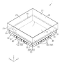
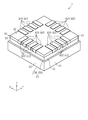
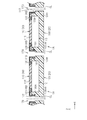
- the perspective view of the semiconductor device of one Embodiment A perspective view of the semiconductor device of FIG. 1 as viewed from the back surface side.
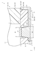
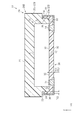
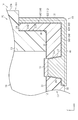
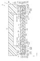
- the back view of the semiconductor device of FIG. Schematic cross-sectional view taken along line 4-4 of FIG. An enlarged view of a part of the plurality of wirings in FIG. 4 and the periphery thereof.
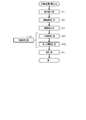
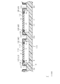
- Schematic cross-sectional view taken along line 6-6 of FIG. The flowchart which shows an example of the manufacturing method of a semiconductor device.
- the explanatory view which shows an example of the element embedding process in the manufacturing method of a semiconductor device.
- the explanatory view which shows an example of the insulating layer formation process in the manufacturing method of a semiconductor device.
- the explanatory view which shows an example of the side surface forming process in the manufacturing method of a semiconductor device.
- the explanatory view which shows an example of the wiring formation process in the manufacturing method of a semiconductor device.
- the explanatory view which shows an example of the wiring formation process in the manufacturing method of a semiconductor device.
- the explanatory view which shows an example of the cutting process in the manufacturing method of a semiconductor device.
- the explanatory view which shows an example of the cutting process in the manufacturing method of a semiconductor device.
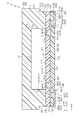
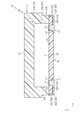
- Schematic cross-sectional view of a modified example semiconductor device. An enlarged view of a part of the plurality of wirings of FIG. 10 and its periphery.
- the explanatory view which shows an example of the element embedding process in the manufacturing method of the semiconductor device of the modification of FIG.
- the explanatory view which shows an example of the insulating layer formation process in the manufacturing method of the semiconductor device of the modification of FIG.
- the explanatory view which shows an example of the cutting process in the manufacturing method of the semiconductor device of the modification of FIG. The explanatory view which shows an example of the element embedding process in another manufacturing method of the semiconductor device of the modification of FIG.
- the explanatory view which shows an example of the insulating layer forming process in another manufacturing method of the semiconductor device of the modification of FIG. The explanatory view which shows an example of the side surface forming process in another manufacturing method of the semiconductor device of the modification of FIG.
- the explanatory view which shows an example of the cutting process in another manufacturing method of the semiconductor device of the modification of FIG. Schematic cross-sectional view of a modified example semiconductor device. Schematic cross-sectional view of a modified example semiconductor device. Schematic cross-sectional view of a modified example semiconductor device. An enlarged view of a part of the plurality of wirings of FIG. 16 and its periphery.
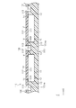
- the semiconductor device 1 includes a semiconductor element 10, a sealing resin 20 that seals a part of the semiconductor element 10, an insulating layer 30 laminated on the sealing resin 20, and an insulating layer 30.
- a plurality of wirings 40 formed in the above are provided.
- the semiconductor device 1 is a Fan-Out type package that is surface-mounted on a wiring board.
- the stacking direction of the sealing resin 20 and the insulating layer 30 is defined as the "thickness direction Z”
- the predetermined direction orthogonal to the thickness direction Z is defined as the “lateral direction X”
- the thickness direction Z and the lateral direction Z is defined as “vertical direction Y”.
- looking from the sealing resin 20 toward the insulating layer 30 in the thickness direction Z is referred to as "plan view”.
- the semiconductor element 10 is, for example, an integrated circuit (IC) such as an LSI (Large Scale Integration). Further, the semiconductor element 10 may be a voltage control circuit such as an LDO (Low Drop Out), an amplification element such as an operational amplifier, or a discrete semiconductor such as a diode.
- IC integrated circuit
- the semiconductor element 10 may be a voltage control circuit such as an LDO (Low Drop Out), an amplification element such as an operational amplifier, or a discrete semiconductor such as a diode.
- LDO Low Drop Out
- amplification element such as an operational amplifier
- a discrete semiconductor such as a diode.
- the shape of the semiconductor element 10 in a plan view is rectangular. In the present embodiment, the shape of the semiconductor element 10 in a plan view is a square.
- the semiconductor element 10 is a flip chip type element.
- the semiconductor element 10 has an element main surface 11 and an element back surface 12 facing opposite sides in the thickness direction Z, and an element side surface 13 formed between the element main surface 11 and the element back surface 12 in the thickness direction Z. ..
- the element side surface 13 intersects the element main surface 11 and the element back surface 12.
- a plurality of (16 in the present embodiment) electrodes 14 are formed on the back surface 12 of the device.
- the plurality of electrodes 14 are conductive to the circuit configured in the semiconductor element 10.
- the plurality of electrodes 14 include, for example, aluminum (Al).
- Al aluminum
- four electrodes 14 are arranged apart from each other along the side surface 13 of each element in a plan view. The number of electrodes 14 can be arbitrarily changed.
- the sealing resin 20 covers a part of the semiconductor element 10. Specifically, the sealing resin 20 covers the element main surface 11 and the element side surface 13 of the semiconductor element 10. On the other hand, the element back surface 12 of the semiconductor element 10 and the plurality of electrodes 14 are exposed from the sealing resin 20.
- the sealing resin 20 is made of a material containing, for example, a black epoxy resin.
- the sealing resin 20 has a resin main surface 21, a resin back surface 22, and a plurality of (four surfaces in this embodiment) resin side surfaces 23.
- the resin main surface 21 faces in the same direction as the element main surface 11 of the semiconductor element 10.
- the resin back surface 22 faces the same direction as the element back surface 12 of the semiconductor element 10.
- the resin side surface 23 intersects the resin main surface 21 and the resin back surface 22.
- the resin side surface 23 faces the same direction as the element side surface 13 of the semiconductor element 10.
- the sealing resin 20 has a first resin portion 20A which is a portion closer to the insulating layer 30 in the thickness direction Z and a portion opposite to the insulating layer 30 in the thickness direction Z. It has two resin portions 20B.
- the first resin portion 20A has a first resin side surface 23a that forms a part of the resin side surface 23.
- the second resin portion 20B is formed larger than the first resin portion 20A in the direction orthogonal to the thickness direction Z.
- the second resin portion 20B has a second resin side surface 23b that forms a part of the resin side surface 23.
- the first resin side surface 23a is located inward of the second resin side surface 23b.
- the sealing resin 20 is provided with a step 24 recessed inside the sealing resin 20 due to the difference in size between the first resin portion 20A and the second resin portion 20B.
- the step 24 is provided over the entire circumferential direction of the sealing resin 20.
- the thickness TR1 of the first resin portion 20A is thinner than the thickness TR2 of the second resin portion 20B. Further, the thickness TR1 is thinner than the thickness TS of the semiconductor element 10.
- the back surface of the first resin portion 20A constitutes the resin back surface 22.
- the main surface of the second resin portion 20B constitutes the resin main surface 21. As shown in FIG. 4, in the present embodiment, the resin back surface 22 is flush with the element back surface 12 of the semiconductor element 10.
- the plurality of electrodes 14 of the semiconductor element 10 project toward the insulating layer 30 from the resin back surface 22.
- the insulating layer 30 is formed in a flat plate shape and is in contact with the resin back surface 22 of the sealing resin 20.
- the insulating layer 30 covers the element back surface 12 of the semiconductor element 10 and the plurality of electrodes 14. In this way, the semiconductor element 10 is sealed by the sealing resin 20 and the insulating layer 30.
- the insulating layer 30 is made of a material containing a thermosetting synthetic resin and an additive containing a metal element that constitutes a part of a plurality of wirings 40.
- the synthetic resin contained in the insulating layer 30 is, for example, an epoxy resin or a polyimide resin.
- the respective sizes of the insulating layer 30 in the horizontal direction X and the vertical direction Y are substantially equal to the respective sizes of the first resin portion 20A in the horizontal direction X and the vertical direction Y.
- the thickness TL of the insulating layer 30 is thinner than the thickness TR of the sealing resin 20. Further, the thickness TL is thinner than the thickness TS of the semiconductor element 10. Further, the thickness TL is thinner than the thickness TR2 of the second resin portion 20B. Further, the thickness TL is thinner than the thickness TR1 of the first resin portion 20A.
- the thickness TR1 of the first resin portion 20A and the thickness TR2 of the second resin portion 20B can be arbitrarily changed. For example, the thickness TR2 may be greater than or equal to the thickness TR1.
- the relationship between the thickness TS of the semiconductor element 10 and the thicknesses TR1 and TR2 can be arbitrarily changed.
- the thickness TS may be a thickness TR1 or less, or may be a thickness TR2 or more.
- the insulating layer 30 has a main surface 31, a back surface 32, and a plurality of side surfaces 33.
- the main surface 31 and the back surface 32 face each other in the thickness direction Z.
- the main surface 31 is in contact with the element back surface 12 of the semiconductor element 10.
- the back surface 32 faces the wiring board when the semiconductor device 1 is mounted on the wiring board.
- Each of the plurality of side surfaces 33 is formed between the main surface 31 and the back surface 32 in the thickness direction Z.
- the plurality of side surfaces 33 are connected to both the main surface 31 and the back surface 32, respectively.
- the plurality of side surfaces 33 face either the horizontal direction X or the vertical direction Y.
- Each side surface 33 intersects the main surface 31 and the back surface 32. Further, the side surface 33 faces the same side as the resin side surface 23 (first resin side surface 23a and second resin side surface 23b) of the sealing resin 20.
- the insulating layer 30 has a plurality of (16 in this embodiment) grooves 34.
- the plurality of grooves 34 have the same shape as each other. Seen from the thickness direction Z, the plurality of grooves 34 have a portion that overlaps with the plurality of electrodes 14 of the semiconductor element 10.
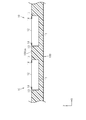
- the plurality of grooves 34 are a back surface side groove 34X recessed from the back surface 32 toward the main surface 31 in the thickness direction Z, and a side surface recessed from the side surface 33 toward the side surface 33 facing the horizontal direction X or the vertical direction Y. It has a gutter 34Z.
- Each side surface of the plurality of grooves 34 is inclined so that the width of the groove 34 gradually expands from the bottom surface of the groove 34 to the opening end of the groove 34.
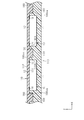
- FIG. 6 is a cross-sectional view of the back surface gutter 34X cut along a plane along the width direction and the thickness direction Z.
- each side surface 34a of the plurality of back surface side grooves 34X is inclined so that the width of the back surface side groove 34X gradually expands from the bottom surface 34b of the back surface side groove 34X to the back surface 32 of the insulating layer 30.
- the dimension C1 of the bottom surface 34b of the back surface side groove 34X in the lateral direction X is the dimension between the boundary between the side surface 34a and the back surface 32 separated from each other in the lateral direction X (width direction of the back surface side groove 34X). It is smaller than C2.
- each of the plurality of side gutters 34Z is the width of the side gutter 34Z extending from the bottom surface of the side gutter 34Z to the side surface 33 of the insulating layer 30 in the same manner as the back surface side groove 34X. Is tilted so that it gradually expands.
- the back surface side groove 34X is provided so as to overlap the electrode 14 of the semiconductor element 10 when viewed from the thickness direction Z.
- the back surface side groove 34X is formed from an inner portion of the semiconductor element 10 on the back surface 32 to the edge in the horizontal direction X or the vertical direction Y of the back surface 32.
- four back surface side grooves 34X are provided so as to be arranged apart from each other along each side surface 33 in a plan view.
- the side gutter 34Z is formed over the entire side surface 33 in the thickness direction Z.
- the side gutter 34Z is connected to the back surface gutter 34X. That is, as shown in FIG. 3, in a plan view, four side gutters 34Z are provided so as to be arranged apart from each other along each side surface 33.
- the portion of the side surface 33 of the insulating layer 30 on which the side surface side groove 34Z is formed is located inward of the first resin side surface 23a of the first resin portion 20A. Further, the portion of the side surface 33 of the insulating layer 30 in which the side surface side groove 34Z is not formed is flush with the first resin side surface 23a.
- a hole 34c communicating with the electrode 14 is formed in a portion of the plurality of grooves 34 that overlaps with the electrode 14 of the semiconductor element 10 in the thickness direction Z.
- the inner side surface forming the hole 34c is inclined so that the inner diameter of the hole 34c gradually increases from the main surface 31 of the insulating layer 30 to the back surface side groove 34X.
- the dimension B1 of the portion of the hole 34c closest to the electrode 14 in the direction orthogonal to the thickness direction Z is larger than the dimension B2 of the portion of the hole 34c closest to the back surface 32 in the direction orthogonal to the thickness direction Z. It becomes smaller.
- the plurality of wirings 40 are electrically connected to the plurality of electrodes 14 of the semiconductor element 10.
- the plurality of wirings 40 form a conductive path for supplying electric power to the semiconductor element 10 and for inputting / outputting signals to / from the semiconductor element 10.
- the plurality of wirings 40 are arranged in the insulating layer 30.
- the plurality of wirings 40 are formed on the insulating layer 30.
- the plurality of wirings 40 are provided in the plurality of grooves 34.
- each of the plurality of wirings 40 has an embedded portion 41 and a rewiring portion 42, respectively.
- the embedded portion 41 is embedded in the insulating layer 30. In the present embodiment, all of the embedded portions 41 are embedded in the insulating layer 30. As shown in FIG. 5, in the present embodiment, the embedded portion 41 is embedded in the hole 34c.
- the side surface of the embedded portion 41 is formed so as to have a shape that follows the shape of the inner side surface that constitutes the hole 34c. That is, the side surface of the embedded portion 41 is inclined so that the diameter of the embedded portion 41 increases from the main surface 31 of the insulating layer 30 toward the back surface side groove 34X.
- the shape of the side surface of the embedded portion 41 is the same as the shape of the inner surface surface forming the hole 34c.
- the embedded portion 41 is connected to the electrode 14 of the semiconductor element 10.
- the rewiring unit 42 is connected to the embedded unit 41.
- the rewiring portion 42 is provided in each of the back surface side groove 34X and the side surface side groove 34Z.
- the rewiring portion 42 includes a portion located outside the semiconductor element 10.
- the rewiring portion 42 has a back surface side rewiring portion 42X provided in the back surface side groove 34X and a side surface side rewiring portion 42Z provided in the side surface side groove 34Z.
- four back surface side rewiring portions 42X are arranged so as to be separated from each other along each side surface 33 of the insulating layer 30.
- four side surface side rewiring portions 42Z are arranged so as to be separated from each other along each side surface 33.
- the back surface side rewiring portion 42X is connected to the side surface side rewiring portion 42Z.
- the back surface side rewiring portion 42X and the side surface side rewiring portion 42Z are integrally formed.
- the side surface side rewiring portion 42Z is formed over the entire side surface 33 of the insulating layer 30 in the thickness direction Z.
- the embedded portion 41 and the rewiring portion 42 each have a base layer 43 and a plating layer 44.
- the base layer 43 is composed of metal elements contained in the additive contained in the insulating layer 30.
- the plating layer 44 is made of, for example, a material containing copper (Cu).
- the base layer 43 of the embedded portion 41 is in contact with the inner side surface forming the hole 34c.
- the plating layer 44 of the embedded portion 41 is surrounded by the base layer 43 of the embedded portion 41 around the thickness direction Z.
- the base layer 43 of the rewiring portion 42 is in contact with the back surface side groove 34X.
- the plating layer 44 of the rewiring portion 42 covers the base layer 43 of the rewiring portion 42.
- the plating layer 44 of the back surface side rewiring portion 42X protrudes from the back surface side groove 34X in the thickness direction Z.
- the plating layer 44 of the side surface side rewiring portion 42Z projects from the side surface side groove 34Z in the direction perpendicular to the side surface 33.
- the plating layer 44 of the side surface side rewiring portion 42Z protrudes from the first resin side surface 23a of the first resin portion 20A in the direction perpendicular to the side surface 33.
- the rewiring portion 42 is made of a metal film including the base layer 43 and the plating layer 44.
- FIG. 6 shows a cross-sectional view of the rewiring portion 42 extending in the vertical direction Y cut along a plane along the thickness direction Z and the horizontal direction X.
- the width direction of the rewiring portion 42 coincides with the lateral direction X.
- the plating layer 44 of the rewiring portion 42 has a recess 45 recessed in the thickness direction of the rewiring portion 42.
- the recess 45 is a trace due to the formation of the plating layer 44 on the base layer 43 covering the plurality of grooves 34 in the wiring forming step in the manufacturing method of the semiconductor device 1 described later.
- the recess 45 is configured to extend along the extending direction of the rewiring portions 42 of the plurality of wirings 40. Specifically, the recess 45 formed in the back surface side rewiring portion 42X is recessed in the thickness direction Z of the plating layer 44 of the back surface side rewiring portion 42X. In FIG. 6, since the back surface side rewiring portion 42X extends in the vertical direction Y, the recess 45 formed in the plating layer 44 of the back surface side rewiring portion 42X extends along the vertical direction Y.
- the rewiring portion 42 extending in the horizontal direction X is formed in the plating layer 44 in a cross-sectional view obtained by cutting the rewiring portion 42 in a plane along the thickness direction Z and the vertical direction Y.
- the recess 45 extends along the lateral direction X of the rewiring portion 42.
- the recess 45 formed in the side surface side rewiring portion 42Z is a side surface.
- the plating layer 44 of the side rewiring portion 42Z is recessed in the lateral direction X.
- the recess 45 formed in the side surface side rewiring portion 42Z is the plating layer of the side surface side rewiring portion 42Z. It is recessed in the vertical direction Y of 44. Since the side surface side rewiring portion 42Z extends in the thickness direction Z, the recess 45 of the side surface side rewiring portion 42Z extends along the thickness direction Z.
- the manufacturing method of the semiconductor device 1 includes an element embedding step (step S1), an insulating layer forming step (step S2), a side surface forming step (step S3), a wiring forming step (step S4), and A cutting step (step S5) is provided.
- the element embedding step (step S1), the insulating layer forming step (step S2), the side surface forming step (step S3), the wiring forming step (step S4), and the cutting step (step S5) are carried out in this order. As a result, the semiconductor device 1 is manufactured.
- a plurality of semiconductor elements 10 are embedded in the sealing resin 100.
- the material of the sealing resin 100 and the plurality of semiconductor elements 10 are arranged in the mold, and then compression molding is performed.
- As the material of the sealing resin 100 a material containing a black epoxy resin is used.
- the portion of each semiconductor element 10 near the element main surface 11 is embedded in the sealing resin 100, and the plurality of electrodes 14 formed on the element back surface 12 and the element back surface 12 are exposed from the sealing resin 100.
- Each semiconductor element 10 is embedded in the sealing resin 100.
- the element main surface 11 and the element side surface 13 of each semiconductor element 10 are covered with the sealing resin 100.
- the sealing resin 100 has a resin back surface 100 bs that is flush with the element back surface 12.
- the plurality of electrodes 14 project from the resin back surface 100 bs in the thickness direction Z.
- an insulating layer 110 is formed which is laminated on the resin back surface 100bs of the sealing resin 100 and covers the element back surface 12 and the plurality of electrodes 14 of the plurality of semiconductor elements 10.
- the material of the insulating layer 110 is composed of a thermosetting synthetic resin and a material containing an additive containing a metal element that constitutes a part of a plurality of wirings 120 described later.
- the synthetic resin of the insulating layer 110 is, for example, an epoxy resin or a polyimide resin.
- the insulating layer 110 is formed by compression molding.
- the insulating layer 110 has a main surface 111 and a back surface 112 facing opposite sides in the thickness direction Z.
- the main surface 111 is the surface of the insulating layer 110 on the sealing resin 100 side.
- the back surface 112 is a surface of the insulating layer 110 opposite to the sealing resin 100 side in the thickness direction Z.
- a separation groove 130 is formed in a portion between the insulating layer 110 and the sealing resin 100 adjacent semiconductor elements 10. Specifically, the portion between the adjacent semiconductor elements 10 in the insulating layer 110 is cut in the thickness direction Z, and the portion between the adjacent semiconductor elements 10 in the sealing resin 100 is in the thickness direction.
- the separation groove 130 is formed by cutting a part of Z.
- the separation groove 130 is formed by dicing. The separation groove 130 is formed so that the bottom surface 131 of the separation groove 130 is located closer to the element back surface 12 than the element main surface 11 of the semiconductor element 10.
- the separation groove 130 forms a first resin portion 100A which is a portion closer to the insulating layer 110 in the thickness direction Z of the sealing resin 100. Further, in the sealing resin 100, the first resin side surface 100xa of the first resin portion 100A is formed by the separation groove 130. Further, in the insulating layer 110, a side surface 113 is formed by the separation groove 130. The side surface 113 is formed between the main surface 111 and the back surface 112 in the thickness direction Z.
- the wiring forming step a plurality of wirings 120 (see FIGS. 8F and 8G) connected to the plurality of electrodes 14 of the semiconductor element 10 are formed.
- the plurality of wirings 120 correspond to the plurality of wirings 40 of the semiconductor device 1.
- the plurality of wirings 120 each have an embedded portion 121 and a rewiring portion 122.
- the embedded portion 121 is embedded in the insulating layer 110 and is connected to the electrode 14 of the semiconductor element 10.
- the embedded portion 121 and the rewiring portion 122 each have a base layer 120A and a plating layer 120B.
- the wiring forming step includes a base layer forming step (step S41) and a plating layer forming step (step S42).
- a plurality of wirings 120 are formed by carrying out the base layer forming step and the plating layer forming step in this order.
- the base layer 120A is deposited by processing the back surface 112 and the side surface 113 of the insulating layer 110.
- the side surface 113 of the insulating layer 110 is an inner surface forming the separation groove 130 of the insulating layer 110.
- a plurality of holes 114 and a plurality of grooves 115 are formed in the insulating layer 110 by a laser.
- the plurality of holes 114 penetrate the insulating layer 110 in the thickness direction Z.
- the plurality of electrodes 14 of the semiconductor element 10 are individually exposed from the plurality of holes 114.
- the plurality of holes 114 are formed by irradiating the insulating layer 110 with a laser until the plurality of electrodes 14 are exposed while recognizing the positions of the plurality of electrodes 14 by an infrared camera or the like.
- the position where the laser is irradiated is corrected one by one based on the position information of the plurality of electrodes 14 obtained by image recognition.
- each groove 115 is recessed from the back surface 112 of the insulating layer 110 in the thickness direction Z, and is connected to a plurality of holes 114, and the back surface side groove 115X and the side surface 113 to the side surface of the insulating layer 110.
- the side gutter 115Z has a side gutter 115Z that is recessed in a direction perpendicular to 113 (horizontal direction X in FIG. 8E).
- the side gutter 115Z is connected to the back surface gutter 115X.
- the plurality of grooves 115 are formed by irradiating the back surface 112 of the insulating layer 110 with a laser.
- the laser is, for example, an ultraviolet laser having a wavelength of 355 nm and a beam diameter of 17 ⁇ m.
- the base layer 120A is composed of metal elements contained in the additive contained in the insulating layer 110.
- the metal element contained in the additive is excited by the laser irradiation. As a result, the metal layer containing the metal element contained in the additive is precipitated as the base layer 120A.
- the plating layer 120B covering the base layer 120A is formed.
- the plating layer 120B is made of a material containing copper.
- the plating layer 120B is formed by electroless plating.
- an embedded portion 121 is formed in each of the plurality of holes 114.
- a rewiring portion 122 is formed in each of the plurality of grooves 115. More specifically, the back surface side rewiring portion 122X is formed in each of the plurality of back surface side grooves 115X, and the side surface side rewiring portion 122Z is formed in each of the plurality of side surface side grooves 115Z.
- a plurality of wirings 120 are formed.
- the insulating layer 110 and the sealing resin 100 are divided into a plurality of pieces by, for example, cutting along the cutting line CL with a dicing blade or the like. As shown in FIG. 8I, the plurality of pieces are arranged in a matrix. As shown in FIG. 8H, the cutting line CL is located inside the separation groove 130 and outside the inner side surface forming the separation groove 130.
- the sealing resin 100 is cut by the dicing blade, the sealing resin 100 has a step 101 in which the first resin portion 100A is recessed, and the first resin portion 100A with respect to the step 101 in the thickness direction Z.
- a second resin portion 100B which is a portion on the opposite side, is formed. Further, by cutting the sealing resin 100, the second resin side surface 100xb of the second resin portion 100B is formed.
- Each of the plurality of divided pieces includes one semiconductor element 10 and a plurality of wirings 120 connected to the semiconductor element 10.
- the sealing resin 100 and the insulating layer 110 that have been made into individual pieces by the cutting step correspond to the sealing resin 20 and the insulating layer 30 of the semiconductor device 1.
- the semiconductor device 1 is manufactured by going through the above steps.
- the operation of this embodiment will be described based on a comparison with a semiconductor device of a comparative example.
- the semiconductor device of the comparative example includes a lead frame, a semiconductor element mounted on the lead frame, and a sealing resin for sealing the semiconductor element and the lead frame.
- the surface of the lead frame is plated to improve the wettability of the solder.
- the semiconductor device of the comparative example is a surface mount type semiconductor device in which the lead frame is exposed on the back surface and the side surface of the sealing resin.
- the plating layer is not formed on the portion of the lead frame exposed from the side surface of the sealing resin. Therefore, when the semiconductor device of the comparative example is mounted on the wiring board by soldering, the solder fillet of the portion of the lead frame exposed from the side surface of the sealing resin is poor and it is difficult to form a solder fillet. As a result, after mounting the semiconductor device of the comparative example on the wiring board, it is difficult to visually recognize the mounted state of the semiconductor device of the comparative example.
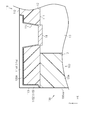
- the side surface side rewiring portion 42Z provided on the side surface 33 of the insulating layer 30 includes the plating layer 44. Therefore, as shown in FIG. 9, when the semiconductor device 1 is mounted on the wiring board CB by the solder SD, the solder SD is likely to be attached to the side surface side rewiring portion 42Z, and the solder fillet SD1 is likely to be formed. Therefore, after the semiconductor device 1 is mounted on the wiring board CB, the mounting state of the semiconductor device 1 can be easily confirmed based on the solder fillet SD1.
- the rewiring portion 42 is formed from the back surface 32 to the side surface 33 of the insulating layer 30. According to this configuration, when the semiconductor device 1 is mounted on the wiring board CB by the solder SD, the solder SD adheres to the side surface side rewiring portion 42Z which is the rewiring portion 42 formed on the side surface 33 and is soldered. Fillet SD1 is formed. The solder fillet SD1 exposed to the outside of the semiconductor device 1 makes it easy to visually recognize the mounted state of the semiconductor device 1.
- the rewiring portion 42 is formed over the entire side surface 33 of the insulating layer 30 in the thickness direction Z. According to this configuration, when the semiconductor device 1 is mounted on the wiring board CB by the solder SD, the solder fillet SD1 formed by adhering the solder SD to the side surface side rewiring portion 42Z becomes large, so that the solder fillet SD1 Is easier to see.
- the side surface side rewiring portion 42Z is located inward of the second resin side surface 23b of the second resin portion 20B. According to this configuration, since the side surface side rewiring portion 42Z is not scraped by the dicing blade in the cutting step, the state in which the plating layer of the side surface side rewiring portion 42Z is formed is maintained. Therefore, when the semiconductor device 1 is mounted on the wiring board CB by the solder SD, the solder SD tends to adhere to the side rewiring portion 42Z. Further, the adhesive area of the solder SD is increased by the side surface side rewiring portion 42Z as compared with the semiconductor device provided with only the back surface side rewiring portion 42X. Therefore, when the semiconductor device 1 is mounted on the wiring board CB by the solder SD, the adhesive force between the semiconductor device 1 and the wiring board CB can be improved.
- the semiconductor device 1 includes an insulating layer 30 having a back surface 32 and a plurality of wirings 40 having an embedded portion 41 and a rewiring portion 42.
- Each of the rewiring portions 42 of the plurality of wirings 40 is arranged on the back surface 32 and is connected to the embedded portions 41 of the plurality of wirings 40 connected to the plurality of electrodes 14 of the semiconductor element 10.
- the insulating layer 30 has a plurality of grooves 34 including a plurality of back surface side grooves 34X recessed from the back surface 32 in the thickness direction Z, and a plurality of side surface side grooves 34Z recessed from the side surface 33 in the direction orthogonal to the side surface 33. ..
- the rewiring portion 42 of the plurality of wirings 40 is in contact with the plurality of grooves 34.
- the plurality of grooves 34 correspond to the plurality of grooves 115 formed in the insulating layer 110 by the laser in the wiring forming step in the manufacturing method of the semiconductor device 1.
- the wiring forming step includes a base layer forming step of precipitating the base layer 120A on the surface of the insulating layer 110 and a plating layer forming step of forming a plating layer 120B covering the base layer 120A.
- the plurality of wirings 120 correspond to the plurality of wirings 40 of the semiconductor device 1.
- the insulating layer 110 is made of a material containing a thermosetting synthetic resin and an additive containing a metal element constituting a part of a plurality of wirings 120 (underlayer layer 120A).
- the base layer forming step by forming the plurality of holes 114 and the plurality of grooves 115 in the insulating layer 110 by a laser, the inner side surfaces forming the plurality of holes 114 and the base layer 120A covering the plurality of grooves 115 are deposited.
- the plurality of holes 114 are formed by exposing the plurality of electrodes 14 while recognizing the positions of the plurality of electrodes 14 of the semiconductor element 10. According to this configuration, even when the semiconductor element 10 is displaced due to the curing shrinkage of the sealing resin 100, the position correction corresponding to the displacement of the plurality of electrodes 14 is performed at the time of laser irradiation by image recognition.
- a plurality of holes 114 in which the plurality of electrodes 14 are exposed can be formed with high accuracy. That is, it is possible to accurately form a plurality of wirings 120 that match the positions of the plurality of electrodes 14. Therefore, the positional deviation at the joint between the plurality of electrodes 14 of the semiconductor element 10 and the plurality of wirings 120 (plurality of wirings 40) can be suppressed.
- the plating layer 120B is formed by electroless plating. According to this configuration, as compared with the case where the plating layer 120B is formed by electrolytic plating, it is not necessary to deposit the base layer 120A which is a conductive path for forming the plating. It can be formed more efficiently.
- the back surface side rewiring portion 42X of the rewiring portion 42 projects in the thickness direction Z with respect to the back surface 32 of the insulating layer 30. According to this configuration, when the semiconductor device 1 is mounted on the wiring board CB, the semiconductor device 1 can be mounted more easily.
- the above-described embodiment is an example of a possible form of the semiconductor device and the method for manufacturing the semiconductor device according to the present disclosure, and is not intended to limit the form.
- the semiconductor device and the method for manufacturing the semiconductor device according to the present disclosure may take a form different from the form exemplified in the above embodiment.
- An example thereof is a form in which a part of the configuration of the above embodiment is replaced, changed, or omitted, or a new configuration is added to the above embodiment.
- the parts common to the above embodiment are designated by the same reference numerals as those in the above embodiment, and the description thereof will be omitted.
- the shape of the insulating layer 30 can be arbitrarily changed.
- the insulating layer 30 may enter the step 24 of the sealing resin 20 as in the semiconductor device 1A shown in FIG.
- the insulating layer 30 covers the first coating portion 35 that covers the resin back surface 22 of the sealing resin 20 and the element back surface 12 of the semiconductor element 10, the side surface 33 of the insulating layer 30, and the first resin side surface 23a of the first resin portion 20A. It has a second covering portion 36.
- the second covering portion 36 covers the entire surface of the first resin side surface 23a.
- the thickness TC2 of the second covering portion 36 is thinner than the thickness TC1 of the first covering portion 35.
- the thickness TC1 of the first covering portion 35 corresponds to the thickness TL of the insulating layer 30 of the above embodiment.
- the back surface side groove 34X is formed in the first covering portion 35, and the side surface side groove 34Z is formed in the second covering portion 36.
- the side gutter 34Z is formed over the entire second covering portion 36 in the thickness direction Z.
- the rewiring portion 42 of the plurality of wirings 40 is formed over the first covering portion 35 and the second covering portion 36.
- the rewiring portion 42 is formed over the entire second covering portion 36 (side surface side groove 34Z) in the thickness direction Z.
- the manufacturing method of the semiconductor device 1A of FIG. 10 includes an element embedding step, an insulating layer forming step, a side surface forming step, a wiring forming step, and a cutting step, similarly to the manufacturing method of the semiconductor device 1 of the above embodiment.
- the semiconductor element 10 is embedded in the sealing resin 100, and a groove 140 is formed in the connecting portion 103 between the adjacent semiconductor elements 10 in the sealing resin 100. Two grooves 140 that are separated from each other are formed in the connecting portion 103.
- the groove 140 is formed from the resin back surface 100bs of the sealing resin 100 in the thickness direction Z.
- compression molding is performed.
- the material of the sealing resin 100 a material containing a black epoxy resin is used.
- the groove 140 may be formed at the same time as the step of embedding the semiconductor element 10 in the sealing resin 100 by a compression molding die. Further, the groove 140 may be formed by dicing after embedding the semiconductor element 10 in the sealing resin 100 by compression molding. The groove 140 is formed so that the bottom surface 141 of the groove 140 is located closer to the element back surface 12 than the element main surface 11 of the semiconductor element 10.
- the groove 140 forms a first resin portion 100A, which is a portion closer to the insulating layer 110 in the thickness direction Z, in the sealing resin 100. Further, in the sealing resin 100, the first resin side surface 100xa of the first resin portion 100A is formed by the groove 140.
- an insulating layer 110 is formed which is laminated on the resin back surface 100bs of the sealing resin 100 and covers the element back surface 12 of the semiconductor element 10 and the plurality of electrodes 14. A part of the insulating layer 110 enters the groove 140. As a result, the first resin side surface 100xa of the first resin portion 100A is covered with a part of the insulating layer 110.
- the material of the insulating layer 110 is composed of a thermosetting synthetic resin and a material containing an additive containing a metal element that constitutes a part of a plurality of wirings 120 described later.
- the synthetic resin of the insulating layer 110 is, for example, an epoxy resin or a polyimide resin.
- the insulating layer 110 is formed by compression molding.
- a separation groove 150 is formed in a portion between the insulating layer 110 and the sealing resin 100 adjacent semiconductor elements 10.
- the separation groove 150 is formed by dicing.
- the separation groove 150 is formed so that the two grooves 140 (see FIG. 12A) formed in the connecting portion 103 communicate with each other.
- the separation groove 150 is formed so that the bottom surface 151 of the separation groove 150 is flush with the bottom surface 141 of the groove 140 (see FIG. 12A).
- a part of the insulating layer 110 that has entered the groove 140 may be removed.
- the insulating layer 110 covers the resin back surface 100bs of the sealing resin 100, the element back surface 12 of the semiconductor element 10, the first coating portion 116 covering the plurality of electrodes 14, and the first resin side surface 100xa of the sealing resin 100. It has a second covering portion 117. Further, in the insulating layer 110, a side surface 113 is formed by the separation groove 150. The side surface 113 is a side surface of the second covering portion 117. The side surface 113 is formed over the entire first resin side surface 100xa of the sealing resin 100 in the thickness direction Z.
- a plurality of wirings 120 are formed in the same manner as in the above embodiment.
- the plurality of wirings 120 are formed over the first covering portion 116 and the second covering portion 117.
- the plurality of wirings 120 are formed over the entire second covering portion 117 in the thickness direction Z.
- the plurality of wirings 120 correspond to the plurality of wirings 40 of the semiconductor device 1A of the modified example.
- the cutting step a plurality of pieces are cut by cutting the insulating layer 110 and the sealing resin 100 with a dicing blade or the like along the cutting line CL, as in the above embodiment. Divide into.
- the cutting line CL is located inside the separation groove 150 and outside the inner side surface forming the separation groove 150. Specifically, the position of the dicing blade and the thickness of the dicing blade are set so that the dicing blade does not come into contact with the wiring 120 formed on the second covering portion 117.
- the sealing resin 100 When the sealing resin 100 is cut by the dicing blade, the sealing resin 100 has a step 101 in which the first resin portion 100A is recessed, and the first resin portion 100A with respect to the step 101 in the thickness direction Z. A second resin portion 100B, which is a portion on the opposite side, is formed. Further, by cutting the sealing resin 100, the second resin side surface 100xb of the second resin portion 100B is formed.
- Each of the plurality of divided pieces includes one semiconductor element 10 and a plurality of wirings 120 connected to the semiconductor element 10.
- the sealing resin 100 and the insulating layer 110 that have been made into individual pieces by the cutting step correspond to the sealing resin 20 and the insulating layer 30 of the semiconductor device 1A. By going through the above steps, the semiconductor device 1A is manufactured.
- the length of the side surface side rewiring portion 42Z in the thickness direction Z can be made longer than the thickness of the insulating layer 30. Therefore, when the semiconductor device 1A is mounted on the wiring board CB by solder SD (both see FIG. 9), the solder fillet SD1 (see FIG. 9) formed by joining the solder to the side rewiring portion 42Z is large. Clearly, since the solder fillet SD1 is easily exposed from the step 24 of the sealing resin 20, it is easy to confirm the mounting state of the semiconductor device 1A on the wiring board CB.
- the side surface side rewiring portion 42Z increases the adhesion area of the solder SD as compared with the semiconductor device provided with only the back surface side rewiring portion 42X. Therefore, when the semiconductor device 1A is mounted on the wiring board CB by the solder SD, the adhesive force between the semiconductor device 1A and the wiring board CB can be improved.
- a dicing blade is used for forming the groove 140 in the element embedding step, a common dicing blade can be used for the dicing for forming the groove 140 and the dicing in the cutting step.
- the manufacturing method of the semiconductor device 1A of FIG. 10 is not limited to the above-mentioned manufacturing method shown in FIGS. 12A to 12E.
- the method for manufacturing the semiconductor device 1A of FIG. 10 may be performed in the order of the steps shown in FIGS. 13A to 13E.
- the manufacturing method of the semiconductor device 1A of FIG. 10 includes an element embedding step, an insulating layer forming step, a side surface forming step, a wiring forming step, and a cutting step, similarly to the manufacturing method described above.
- the semiconductor element 10 is embedded in the sealing resin 100, and a groove 160 is formed in the connecting portion 103 between the adjacent semiconductor elements 10 in the sealing resin 100.
- the groove 160 is formed from the resin back surface 100bs of the sealing resin 100 in the thickness direction Z.
- the width of the groove 160 in the lateral direction X is larger than the width of each of the two grooves 140 (see FIG. 12A) in the lateral direction X.
- the width of the groove 160 in FIG. 13A in the lateral direction X is, for example, equal to the distance connecting two grooves 140 adjacent to each other in the lateral direction X in FIG. 12A in the lateral direction X.
- the groove 160 is formed so that its bottom surface 161 is located closer to the element back surface 12 than the element main surface 11 of the semiconductor element 10.
- the first resin portion 100A which is a portion closer to the insulating layer 110 in the thickness direction Z, is formed by the groove 160. Further, in the sealing resin 100, the first resin side surface 100xa of the first resin portion 100A is formed by the groove 160.
- the element embedding step after arranging the material of the sealing resin 100 and the semiconductor element 10 in the mold, compression molding is performed.
- the material of the sealing resin 100 a material containing a black epoxy resin is used.
- a portion of the semiconductor element 10 near the element main surface 11 is embedded in the sealing resin 100, and a plurality of electrodes 14 formed on the element back surface 12 and the element back surface 12 are exposed from the resin back surface 100bs of the sealing resin 100.
- the semiconductor element 10 is embedded in the sealing resin 100.
- the groove 160 may be formed at the same time as the step of embedding the semiconductor element 10 in the sealing resin 100 by a compression molding die. Further, the groove 160 may be formed by dicing after embedding the semiconductor element 10 in the sealing resin 100 by compression molding.
- an insulating layer 110 is formed which is laminated on the resin back surface 100bs of the sealing resin 100 and covers the element back surface 12 of the semiconductor element 10 and the plurality of electrodes 14. A part of the insulating layer 110 enters the groove 160. As a result, the first resin side surface 100xa of the first resin portion 100A is covered with a part of the insulating layer 110.
- the material of the insulating layer 110 is composed of a thermosetting synthetic resin and a material containing an additive containing a metal element that constitutes a part of a plurality of wirings 120 described later.
- the synthetic resin of the insulating layer 110 is, for example, an epoxy resin or a polyimide resin.
- the insulating layer 110 is formed by compression molding.
- a separation groove 170 is formed in a portion between the insulating layer 110 and the sealing resin 100 adjacent semiconductor elements 10.
- the separation groove 170 is formed by dicing.
- the separation groove 170 is formed by dicing the insulating layer 110 that has entered the groove 160 (see FIG. 13A) formed in the connecting portion 103.
- the thickness of the dicing blade forming the separation groove 170 in the lateral direction X is thinner than the thickness of the dicing blade forming the groove 160 in the lateral direction X. Therefore, the width of the separation groove 170 in the lateral direction X is smaller than the width of the groove 160 in the lateral direction X.
- the separation groove 170 is formed so that the bottom surface 171 thereof is flush with the bottom surface 161 of the groove 160 (see FIG. 13A).
- the insulating layer 110 covers the resin back surface 100bs of the sealing resin 100, the element back surface 12 of the semiconductor element 10, the first coating portion 116 covering the plurality of electrodes 14, and the first resin side surface 100xa of the sealing resin 100. It has a second covering portion 117.
- a side surface 113 is formed by the separation groove 170.
- the side surface 113 is a side surface of the second covering portion 117.
- the side surface 113 is formed over the entire first resin side surface 100xa of the sealing resin 100 in the thickness direction Z.
- the width of the separation groove 170 in the lateral direction X and the depth in the thickness direction Z are equal to the width of the separation groove 150 (see FIG. 12C) in the lateral direction X and the depth in the thickness direction Z, respectively.
- a plurality of wirings 120 are formed in the same manner as in the wiring forming step shown in FIG. 12D.
- the plurality of wirings 120 are formed over the first covering portion 116 and the second covering portion 117.
- the plurality of wirings 120 are formed over the entire second covering portion 117 in the thickness direction Z.
- the plurality of wirings 120 correspond to the plurality of wirings 40 of the semiconductor device 1A of the modified example.
- the insulating layer 110 and the sealing resin 100 are cut by, for example, a dicing blade or the like along the cutting line CL. Divide into pieces.
- the cutting line CL is located inside the separation groove 170 and outside the inner side surface forming the separation groove 170. Specifically, the position of the dicing blade and the thickness of the dicing blade in the lateral direction X are set so that the dicing blade does not come into contact with the wiring 120 formed on the second covering portion 117.
- the thickness of the dicing blade that cuts the sealing resin 100 in the lateral direction X is thinner than the thickness of the dicing blade that forms the separation groove 170 in the lateral direction X.
- the sealing resin 100 is cut by the dicing blade, the sealing resin 100 has a step 101 in which the first resin portion 100A is recessed, and the first resin portion 100A with respect to the step 101 in the thickness direction Z.
- a second resin portion 100B which is a portion on the opposite side, is formed. Further, by cutting the sealing resin 100, the second resin side surface 100xb of the second resin portion 100B is formed.
- Each of the plurality of divided pieces includes one semiconductor element 10 and a plurality of wirings 120 connected to the semiconductor element 10.
- the sealing resin 100 and the insulating layer 110 that have been made into individual pieces by the cutting step correspond to the sealing resin 20 and the insulating layer 30 of the semiconductor device 1A. By going through the above steps, the semiconductor device 1A is manufactured.
- the same effect as the manufacturing method of the semiconductor device 1A of FIGS. 12A to 12E can be obtained.
- the number of scanning lines of the dicing blade is two.
- the groove 160 is formed by the dicing blade, the number of scanning lines of the dicing blade becomes one, and the number of lines can be reduced. Therefore, the element embedding process can be simplified.
- the thickness TC2 of the second covering portion 36 of the insulating layer 30 can be arbitrarily changed.
- the thickness TC2 may be greater than or equal to the distance between the first resin side surface 23a of the first resin portion 20A of the sealing resin 20 and the second resin side surface 23b of the second resin portion 20B. That is, the side surface 33 (side surface of the second coating portion 36) of the insulating layer 30 may be flush with the second resin side surface 23b, and the side surface 33 (side surface of the second coating portion 36) may be flush with the second resin side surface 23b.
- the insulating layer 30 may be provided so as to project outward.
- the length of the second covering portion 36 of the insulating layer 30 in the thickness direction Z can be arbitrarily changed.
- the second coating portion 36 may be configured to cover a part of the first resin side surface 23a of the first resin portion 20A on the resin back surface 22 side in the thickness direction Z.
- an insulating layer having a multi-layer structure may be used instead of the insulating layer 30 having a one-layer structure.
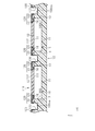
- the semiconductor device 1B shown in FIG. 14 has a first insulating layer 30A and a second insulating layer 30B laminated with each other in the thickness direction Z.
- the first insulating layer 30A and the second insulating layer 30B are laminated on the sealing resin 20 in this order.
- the first insulating layer 30A is arranged closer to the semiconductor element 10 than the second insulating layer 30B.
- the first insulating layer 30A covers the sealing resin 20, the element back surface 12 of the semiconductor element 10, and the plurality of electrodes 14.
- the first insulating layer 30A is provided with a plurality of first wirings 40A made of a metal film.
- the second insulating layer 30B is provided with a plurality of second wirings 40B made of a metal film.
- the first insulating layer 30A is made of a material containing a thermosetting synthetic resin and an additive containing a metal element that constitutes a part of a plurality of first wirings 40A.
- the second insulating layer 30B is made of a material containing a thermosetting synthetic resin and an additive containing a metal element that constitutes a part of a plurality of second wirings 40B.
- the thermosetting synthetic resin of the first insulating layer 30A and the second insulating layer 30B is, for example, an epoxy resin or a polyimide resin.
- the first insulating layer 30A and the second insulating layer 30B are preferably made of the same material.
- the first insulating layer 30A is formed between the first main surface 31a and the first back surface 32a facing opposite sides in the thickness direction Z, and the thickness direction Z between the first main surface 31a and the first back surface 32a. It has a first side surface 33a.
- the first main surface 31a constitutes the main surface 31 of the insulating layer 30.
- the first side surface 33a forms a part of the side surface 33 of the insulating layer 30.
- the first insulating layer 30A is orthogonal to the first back surface side groove 34XA recessed from the first back surface 32a of the first insulating layer 30A in the thickness direction Z and the first side surface 33a of the first insulating layer 30A in the thickness direction Z. It has a first groove 34d including a first side surface side groove 34ZA recessed in a direction (thickness direction of the first insulating layer 30A).
- the cross-sectional structure when the first back surface gutter 34XA is cut in a plane along the width direction and the thickness direction Z of the first back surface gutter 34XA is a plane along the width direction and the thickness direction Z of the back surface side groove 34X of the above embodiment.
- the first back surface side groove 34XA is provided so as to overlap the electrode 14 of the semiconductor element 10 when viewed from the thickness direction Z.
- the first back surface side groove 34XA is formed from an inner portion of the semiconductor element 10 on the first back surface 32a to an outer portion of the semiconductor element 10 and an inner portion of the first side surface 33a.
- a hole 34cd communicating with the electrode 14 is formed in a portion of the plurality of first back surface side grooves 34XA that overlaps with the electrode 14 of the semiconductor element 10 in the thickness direction Z.
- the inner surface forming the hole 34cd is inclined so that the inner diameter of the hole 34cd increases from the first main surface 31a of the first insulating layer 30A (main surface 31 of the insulating layer 30) to the first back surface 32a. ..
- the shape of the inner surface forming the hole 34cd is the same as the shape of the inner surface forming the hole 34c of the above embodiment.
- the first side surface gutter 34ZA is not connected to the first back surface side groove 34XA.
- the first side surface side groove 34ZA corresponding to the first back surface side groove 34XA extending in the lateral direction X among the plurality of first back surface side grooves 34XA overlaps with the first back surface side groove 34XA extending in the lateral direction X when viewed from the lateral direction X. ..
- the first side surface gutter 34ZA corresponding to the first back surface side groove 34XA extending in the lateral direction X is separated from the first back surface side groove 34XA extending in the lateral direction X in the lateral direction X.
- the portion of the first side surface 33a of the first insulating layer 30A on which the first side surface side groove 34ZA is formed is located inward of the first resin side surface 23a of the first resin portion 20A. Further, the portion of the first side surface 33a of the first insulating layer 30A in which the first side surface side groove 34ZA is not formed is flush with the first resin side surface 23a.
- the first side surface gutter 34ZA corresponding to the first back surface side groove 34XA extending in the lateral direction X is separated from the first back surface side groove 34XA extending in the lateral direction X in the lateral direction X.
- the first side surface side groove 34ZA is formed over the entire first side surface 33a of the first insulating layer 30A in the thickness direction Z.
- the cross-sectional structure when the first side surface side groove 34ZA is cut in the width direction of the first side surface side groove 34ZA and the direction orthogonal to the first side surface 33a and the width direction is the width direction of the side surface side groove 34Z of the above embodiment. It is the same as the cross-sectional structure when the side surface side groove 34Z is cut in the side surface 33 and the plane along the direction orthogonal to the width direction.
- Each of the plurality of first wirings 40A has a first embedded portion 41a and a first rewiring portion 42a. At least a part of the first embedded portion 41a is embedded in the first insulating layer 30A. In FIG. 14, all of the first embedded portion 41a is embedded in the first insulating layer 30A. The first embedded portion 41a is embedded in the hole 34cd. The first embedded portion 41a is connected to the electrode 14 of the semiconductor element 10. The first rewiring portion 42a is provided on the first back surface 32a and is connected to the first embedded portion 41a. The first rewiring portion 42a is in contact with the first groove 34d.
- the first rewiring portion 42a has a first back surface side rewiring portion 42XA in contact with the first back surface side groove 34XA and a first side surface side rewiring portion 42ZA in contact with the first side surface side groove 34ZA.
- the first back surface side rewiring portion 42XA is not connected to the first side surface side rewiring portion 42ZA.
- the first back surface side rewiring portion 42XA is in contact with the entire first back surface side groove 34XA in the direction in which the first back surface side groove 34XA extends. Therefore, the first back surface side rewiring portion 42XA includes a portion located outside the semiconductor element 10.
- the second insulating layer 30B is formed between the second main surface 31b and the second back surface 32b facing opposite sides in the thickness direction Z, and the thickness direction Z between the second main surface 31b and the second back surface 32b. It has a second side surface 33b.
- the second main surface 31b is in contact with the first back surface 32a of the first insulating layer 30A.
- the second back surface 32b constitutes the back surface 32 of the insulating layer 30.
- the second side surface 33b forms a part of the side surface 33 of the insulating layer 30.
- the second insulating layer 30B is orthogonal to the second back surface side groove 34XB recessed from the second back surface 32b of the second insulating layer 30B in the thickness direction Z and the second side surface 33b of the second insulating layer 30B in the thickness direction Z. It has a second groove 34e including a second side surface side groove 34ZB that is recessed in the direction (thickness direction of the second insulating layer 30B).
- the cross-sectional structure when the second back surface side groove 34XB is cut in the plane along the width direction and the thickness direction Z of the second back surface side groove 34XB is the plane along the width direction and the thickness direction Z of the back surface side groove 34X of the above embodiment.
- the second back surface side groove 34XB is provided so as to overlap the first groove 34d of the first insulating layer 30A when viewed from the thickness direction Z.
- the second back surface side groove 34XB is formed on the second back surface 32b from the inner portion of the first groove 34d to the outer portion of the first groove 34d.
- a hole 34ce communicating with the second back surface side groove 34XB is formed in a portion of the plurality of second back surface side grooves 34XB that overlaps with the hole 34cd of the second back surface side groove 34XB in the thickness direction Z.
- a taper is formed on the inner side surface forming the hole 34ce from the second main surface 31b of the second insulating layer 30B to the second back surface side groove 34XB.
- the tapered shape of the hole 34ce is the same as the tapered shape of the hole 34c of the above embodiment.
- the second side surface gutter 34ZB is connected to the second back surface side groove 34XB.
- the second side surface gutter 34ZB is formed over the entire second side surface 33b in the thickness direction Z.
- the portion of the second side surface 33b of the second insulating layer 30B on which the second side surface side groove 34ZB is formed is located inward of the first resin side surface 23a of the first resin portion 20A.
- the second side surface side groove 34ZB is flush with the first side surface side groove 34ZA of the first insulating layer 30A.
- the portion of the second side surface 33b of the second insulating layer 30B in which the second side surface side groove 34ZB is not formed is flush with the first resin side surface 23a.
- the second side surface gutter 34ZB is connected to the first side surface side groove 34ZA.
- the cross-sectional structure when the second side surface side groove 34ZB is cut in the width direction of the second side surface side groove 34ZB and the plane along the direction orthogonal to the second side surface 33b and the width direction is the width direction of the side surface side groove 34Z of the above embodiment. It is the same as the cross-sectional structure when the side surface side groove 34Z is cut in the side surface 33 and the plane along the direction orthogonal to the width direction.
- the plurality of second wirings 40B each have a second embedded portion 41b and a second rewiring portion 42b. At least a part of the second embedded portion 41b is embedded in the second insulating layer 30B. In FIG. 14, all of the second embedded portion 41b is embedded in the second insulating layer 30B. The second embedded portion 41b is embedded in the hole 34ce. The second embedded portion 41b is connected to the first back surface side rewiring portion 42XA of the first insulating layer 30A. The second rewiring portion 42b is provided on the second back surface 32b and is connected to the second embedded portion 41b. The second rewiring portion 42b is located outside the semiconductor element 10.
- the second rewiring portion 42b includes a portion located outside the first rewiring portion 42a.
- the second rewiring portion 42b includes a second back surface side rewiring portion 42XB provided on the second back surface 32b and a second side surface side rewiring portion 42ZB provided on the second side surface 33b of the second insulating layer 30B.
- the second back surface side rewiring portion 42XB is connected to the second side surface side rewiring portion 42ZB.
- the second back surface side rewiring portion 42XB and the second side surface side rewiring portion 42ZB are integrally formed.
- the first side surface side rewiring portion 42ZA and the second side surface side rewiring portion 42ZB are connected to each other.
- the side rewiring portion 42ZA can also be regarded as a part of the second rewiring portion 42b. Therefore, the second rewiring portion 42b extends from the second back surface 32b of the second insulating layer 30B to the first side surface 33a of the first insulating layer 30A and the second side surface 33b of the second insulating layer 30B in the thickness direction Z. It can be said that it extends over. In this case, it can be said that the first rewiring portion 42a is formed only on the first back surface 32a of the first insulating layer 30A.
- the second rewiring portion 42b is in contact with the second groove 34e. More specifically, the second back surface side rewiring portion 42XB is in contact with the second back surface side groove 34XB.
- the second side surface side rewiring portion 42ZB is in contact with the second side surface side groove 34ZB.
- the second side surface side rewiring portion 42ZB is in contact with the entire second side surface side groove 34ZB in the thickness direction Z. That is, the second side surface side rewiring portion 42ZB is formed over the entire second side surface 33b in the thickness direction Z.
- the second side surface side rewiring portion 42ZB is connected to the first side surface side rewiring portion 42ZA provided in the first insulating layer 30A.
- the second side surface side rewiring portion 42ZB and the first side surface side rewiring portion 42ZA are integrally formed.
- the method for forming the 42b is the same as the method for forming the embedded portion 41 and the rewiring portion 42 of the plurality of wirings 40 of the above embodiment. That is, the first embedded portion 41a, the first rewiring portion 42a, the second embedded portion 41b, and the second rewiring portion 42b are metal films having a base layer 43 and a plating layer 44 (both see FIG. 5), respectively. Consists of.
- the manufacturing method of the semiconductor device 1B is different in the insulating layer forming step, the side surface forming step, and the wiring forming step as compared with the manufacturing method of the semiconductor device 1 of the above embodiment.
- the method for manufacturing the semiconductor device 1B includes a first insulating layer forming step for forming the first insulating layer 30A and a first wiring forming step for forming the first back surface side rewiring portion 42XA of the first wiring 40A. It has a second insulating layer forming step of forming the second insulating layer 30B, and a second wiring forming step of forming the first side surface side rewiring portion 42ZA of the second wiring 40B and the first wiring 40A.
- the element embedding step, the first insulating layer forming step, the first wiring forming step, the second insulating layer forming step, the side surface forming step, the second wiring forming step, and the cutting step are carried out in this order.
- the side surface forming step the first side surface 33a of the first insulating layer 30A and the second side surface 33b of the second insulating layer 30B are formed.
- the second wiring forming step the first side surface side rewiring portion 42ZA of the first wiring 40A and the second side surface side rewiring portion 42ZB of the second wiring 40B are formed.
- the structure is a plurality of layers including the first insulating layer 30A and the second insulating layer 30B
- the plurality of first wirings 40A and the plurality of second wirings 40B are arranged in a plurality of layers in the thickness direction Z. Can be done. Therefore, when viewed from the thickness direction Z, the second back surface side rewiring portion 42XB of the plurality of second wiring 40B may be arranged so as to overlap the first back surface side rewiring portion 42XA of the plurality of first wiring 40A. it can. Therefore, a complicated wiring pattern can be taken as compared with the case of one insulating layer.
- the semiconductor device 1B is mounted on the wiring board CB by solder SD (both see FIG. 9)
- the first side surface side rewiring portion 42ZA of the first insulating layer 30A and the second side surface side rewiring portion of the second insulating layer 30B are rewired.
- the solder fillet SD1 becomes large. Therefore, since the solder fillet SD1 is easily exposed from the step 24 of the sealing resin 20, it is easy to confirm the mounting state of the semiconductor device 1B on the wiring board CB.
- the length of the first side surface side rewiring portion 42ZA in the thickness direction Z can be arbitrarily changed.
- the first side surface side rewiring portion 42ZA may be formed from the second back surface 32b of the second insulating layer 30B to a part of the first side surface 33a of the first insulating layer 30A in the thickness direction Z.
- the first side surface side groove 34ZA of the first insulating layer 30A is formed from the first back surface 32a of the first insulating layer 30A to a part of the thickness direction Z of the first side surface 33a.
- the first side surface side rewiring portion 42ZA may be omitted. That is, only the second side surface side rewiring portion 42ZB is formed. In this case, the first side surface side groove 34ZA of the first insulating layer 30A is not formed. Therefore, the first side surface 33a of the first insulating layer 30A is flush with the first resin side surface 23a of the first resin portion 20A.
- the resin material constituting the first insulating layer 30A can be arbitrarily changed.
- the first insulating layer 30A may be a material containing no additives containing a metal element that constitutes a part of the plurality of first wirings 40A.
- a base layer made of a metal thin film may be deposited on the first back surface 32a of the first insulating layer 30A. Then, a plurality of first wirings 40A are formed by forming a plating layer on the base layer.
- the insulating layer having a three-layer structure or more may be used instead of the insulating layer having a two-layer structure.
- the shape of the side surface 33 of the insulating layer 30 can be arbitrarily changed.
- the side surface 33 includes an inclined surface 33x inclined with respect to the thickness direction Z.
- the inclined surface 33x is inclined outward from the back surface 32 of the insulating layer 30 toward the main surface 31.
- the side surface 33 is composed of an inclined surface 33x.
- the side surface side rewiring portion 42Z formed on the inclined surface 33x is inclined outward from the back surface 32 of the insulating layer 30 toward the main surface 31.
- a part of the side surface 33 may be formed of an inclined surface 33x.
- an inclined surface 33x is formed on the side surface 33 of the insulating layer 30 on which the side surface side rewiring portion 42Z is formed.
- the back surface side groove 34X when the back surface side groove 34X is formed by irradiating the back surface 32 with the laser along the direction perpendicular to the back surface 32 of the insulating layer 30 (thickness direction Z), the irradiation direction of the laser is changed.
- the side groove 34Z can be formed on the inclined surface 33x. Therefore, the wiring forming step can be simplified as compared with the case where the irradiation direction of the laser forming the back surface side groove 34X and the irradiation direction of the laser forming the side surface side groove 34Z are different.
- the step 24 may be omitted from the sealing resin 20.
- the sealing resin 20 the first resin portion 20A and the second resin portion 20B are not classified.
- a step is formed between the insulating layer 30 and the sealing resin 20. That is, a step is formed in which the insulating layer 30 is recessed inward with respect to the sealing resin 20 due to the difference in size between the insulating layer 30 and the sealing resin 20. Therefore, the side surface 33 of the insulating layer 30 is located inward of the resin side surface 23 of the sealing resin 20.
- the side surface forming step only the insulating layer 110 is cut to form the separation groove 130.
- the separation groove 130 forms a side surface 113 of the insulating layer 110 (side surface 33 of the insulating layer 30). Then, in the cutting step, by cutting only the sealing resin 100 in the thickness direction Z, a step is formed between the sealing resin 100 and the insulating layer 110, and the side surface of the sealing resin 100 (the resin side surface of the sealing resin 20). 23) is formed.
- the method of forming a plurality of wirings 40 (a plurality of first wirings 40A and a plurality of second wirings 40B) can be arbitrarily changed. ..
- a plurality of wirings 40 are formed by printing the back surface 32 and the side surface 33 of the insulating layer 30 with ink containing metal particles, respectively.
- an inkjet method in which the ink is ejected toward the back surface 32 and the side surface 33 can be used.
- a plurality of parts of the metal film other than the portion where the plurality of wirings 40 are formed are removed. Wiring 40 is formed.
- Inclined surface 34 ... Groove 34X ... Back surface side groove 34XA ... First back surface side groove 34XB ... Second back surface side groove 34Z ... Side surface side groove 34ZA ... First side surface side groove 34ZB ... Second side surface side groove 34c ... Hole 34d ... First groove 34e ... Second groove 35 ... First covering portion 36 ... Second covering portion 40 ... Wiring 40A ... Multiple first wiring 40B ... Multiple second wiring 41 ... Embedded portion 41a ... First 1 Embedded part 41b ... Second embedded part 42 ... Rewiring part 42a ... First rewiring part 42b ... Second rewiring part 42X ... Back side rewiring part 42XA ...
- Second coating portion 120 ... Wiring 120A ... Base layer 120B ... Plating layer 121 ... Embedded portion 122 ... Rewiring portion 122X ... Back side rewiring portion 122Z ... Side side rewiring portion 122 Wiring part 130 ... Separation groove 131 ... Bottom surface 150 ... Separation groove 151 ... Bottom surface Z ... Thickness direction
Landscapes
- Structures Or Materials For Encapsulating Or Coating Semiconductor Devices Or Solid State Devices (AREA)
- Engineering & Computer Science (AREA)
- Manufacturing & Machinery (AREA)
- Microelectronics & Electronic Packaging (AREA)
Abstract
半導体装置(1)は、絶縁層(30)と、複数の配線(40)と、半導体素子(10)と、封止樹脂(20)とを備える。絶縁層(30)は、厚さ方向(Z)において互いに反対側を向く主面(31)及び裏面(32)、並びに主面(31)と裏面(32)との厚さ方向(Z)の間に形成された側面(33)を有する。複数の配線(40)は、絶縁層(30)に埋め込まれた埋込部(41)、及び裏面(32)から側面(33)までにわたり形成され、埋込部(41)に繋がる金属膜からなる再配線部(42)を有する。半導体素子(10)は、複数の配線(40)の埋込部(41)の少なくとも一部に繋がる複数の電極(14)を有し、主面(31)に搭載される。封止樹脂(20)は、主面(31)に接し、かつ半導体素子(10)を覆う。
Description
本開示は、半導体装置及び半導体装置の製造方法に関する。
近年の電子機器の小型化に伴い、電子機器に用いられる半導体装置の小型化が進められている。そこで、複数の電極を有する半導体素子と、半導体素子のうちの複数の電極が形成される裏面を覆う絶縁層と、絶縁層に形成されるとともに複数の電極と電気的に接続され、半導体素子よりも外方に位置する複数の配線とを備える、いわゆるFan-Out型の半導体装置が提案されている。これにより、半導体装置の小型化を図りつつ、半導体装置が実装される配線基板の配線パターンの形状に柔軟に対応できる。
ところで、例えば特許文献1の半導体装置では、複数の配線に接続される端子が絶縁層の裏面から露出する構成であるため、半田によって半導体装置が配線基板に実装される場合、半導体装置の外部から半田が視認し難い。このため、半田による半導体装置と配線基板との接合状態から半導体装置の配線基板への実装状態を視認する観点において改善の余地がある。
本開示の目的は、半導体装置の配線基板への実装状態を容易に確認できる半導体装置及び半導体装置の製造方法を提供することにある。
上記課題を解決する半導体装置は、絶縁層と、複数の配線と、半導体素子と、封止樹脂と、を含む。前記絶縁層は、厚さ方向において互いに反対側を向く主面及び裏面、並びに前記主面と前記裏面との前記厚さ方向の間に形成された側面を有する。前記複数の配線は、前記絶縁層に少なくとも一部が埋め込まれた埋込部、及び前記裏面から前記側面までにわたり形成され、前記埋込部に繋がる金属膜からなる再配線部を有する。前記半導体素子は、前記複数の配線の前記埋込部の少なくとも一部に繋がる複数の電極を有し、前記主面に搭載される。前記封止樹脂は、前記主面に接し、かつ前記半導体素子を覆う。
この構成によれば、半導体装置が配線基板に半田によって実装される場合に、絶縁層の側面に形成された再配線部に半田が付着することによって半田フィレットが形成される。半導体装置の外部に露出する半田フィレットによって、半導体装置を配線基板に接合する半田が視認できる。したがって、半導体装置の実装状態を容易に視認できる。
上記課題を解決する半導体装置は、第1絶縁層と、第2絶縁層と、第1埋込部と、第1再配線部と、第2埋込部と、第2再配線部と、半導体素子と、封止樹脂と、を含む。前記第1絶縁層は、厚さ方向において互いに反対側を向く第1主面及び第1裏面、並びに前記第1主面と前記第1裏面との前記厚さ方向の間に形成された第1側面を有する。前記第2絶縁層は、前記厚さ方向において前記第1絶縁層に積層され、前記厚さ方向において互いに反対側を向く第2主面及び第2裏面、並びに前記第2主面と前記第2裏面との前記厚さ方向の間に形成された第2側面を有する。前記第1埋込部の少なくとも一部は、前記第1絶縁層に埋め込まれている。前記第1再配線部は、前記第1絶縁層の少なくとも前記第1裏面に形成され、かつ前記第1埋込部に繋がる金属膜からなる。前記第2埋込部の少なくとも一部は、前記第2絶縁層に埋め込まれ、前記第2埋込部は、前記第1再配線部に繋がる。前記第2再配線部は、前記第2裏面から前記第2側面までにわたり形成され、かつ前記第2埋込部に繋がる金属膜からなる。前記半導体素子は、前記第1埋込部の少なくとも一部に繋がる電極を有し、前記第1主面に搭載される。前記封止樹脂は、前記第1主面に接し、かつ前記半導体素子を覆う。
この構成によれば、半導体装置が配線基板に半田によって実装される場合に、第2絶縁層の第2側面に形成された第2再配線部に半田が付着することによって半田フィレットが形成される。半導体装置の外部に露出する半田フィレットによって、半導体装置を配線基板に接合する半田が視認できる。したがって、半導体装置の実装状態を容易に視認できる。
上記課題を解決する半導体装置の製造方法は、半導体素子を、樹脂裏面側から前記半導体素子の厚さ方向の一方に設けられた電極が露出するように封止樹脂に埋め込む素子埋込工程と、前記封止樹脂の前記樹脂裏面及び前記電極を覆う主面及び前記主面と反対側を向く裏面とを有する絶縁層を形成する絶縁層形成工程と、前記絶縁層に前記裏面と交差する側面を形成する側面形成工程と、前記絶縁層に埋め込まれ、かつ前記電極に繋がる埋込部、及び前記裏面から前記側面までにわたる再配線部を形成する配線形成工程と、を備えた。
この構成によれば、半導体装置が配線基板に半田によって実装される場合に、絶縁層の側面に形成された再配線部に半田が付着することによって半田フィレットが形成される。半導体装置の外部に露出する半田フィレットによって、半導体装置を配線基板に接合する半田が視認できる。したがって、半導体装置の実装状態を容易に視認できる。
上記半導体装置及び半導体装置の製造方法によれば、半導体装置の配線基板への実装状態を容易に確認できる。
以下、半導体装置及び半導体装置の製造方法の実施形態について図面を参照して説明する。以下に示す実施形態は、技術的思想を具体化するための構成や方法を例示するものであり、各構成部品の材質、形状、構造、配置、寸法等を下記のものに限定するものではない。以下の実施形態は、種々の変更を加えることができる。
[実施形態]
(半導体装置の構成)
図1~図6を参照して、一実施形態の半導体装置の構成について説明する。
(半導体装置の構成)
図1~図6を参照して、一実施形態の半導体装置の構成について説明する。
図1及び図2に示すように、半導体装置1は、半導体素子10、半導体素子10の一部を封止する封止樹脂20、封止樹脂20に積層された絶縁層30、及び絶縁層30に形成された複数の配線40を備える。半導体装置1は、配線基板に表面実装されるFan-Out型のパッケージである。
なお、以降の説明において、封止樹脂20及び絶縁層30の積層方向を「厚さ方向Z」とし、厚さ方向Zと直交する所定方向を「横方向X」とし、厚さ方向Z及び横方向Xと直交する方向を「縦方向Y」と定義する。また厚さ方向Zにおいて封止樹脂20から絶縁層30に向けてみることを「平面視」とする。
半導体素子10は、例えば、LSI(Large Scale Integration)などの集積回路(IC)である。また半導体素子10は、LDO(Low Drop Out)などの電圧制御回路や、オペアンプなどの増幅素子、ダイオードなどのディスクリート半導体であってもよい。平面視における半導体素子10の形状は、矩形状である。本実施形態では、平面視における半導体素子10の形状は正方形である。半導体素子10は、フリップチップ型の素子である。
半導体素子10は、厚さ方向Zにおいて互いに反対側を向く素子主面11、素子裏面12、及び素子主面11と素子裏面12との厚さ方向Zの間に形成された素子側面13を有する。素子側面13は、素子主面11及び素子裏面12と交差している。図3に示すように、素子裏面12には、複数(本実施形態では16個)の電極14が形成されている。複数の電極14は、半導体素子10に構成された回路に導通している。複数の電極14は、例えばアルミニウム(Al)を含む。図3に示すとおり、本実施形態では、平面視において、各素子側面13に沿って4個の電極14が互いに離間して配列されている。なお、電極14の個数は任意変更可能である。
図1~図4に示すように、封止樹脂20は、半導体素子10の一部を覆っている。具体的には、封止樹脂20は、半導体素子10の素子主面11及び素子側面13を覆っている。一方、半導体素子10の素子裏面12及び複数の電極14は、封止樹脂20から露出している。封止樹脂20は、例えば黒色のエポキシ樹脂を含む材料からなる。封止樹脂20は、樹脂主面21、樹脂裏面22、及び複数(本実施形態では4面)の樹脂側面23を有する。樹脂主面21は、半導体素子10の素子主面11と同じ方向を向く。樹脂裏面22は、半導体素子10の素子裏面12と同じ方向を向く。樹脂側面23は、樹脂主面21及び樹脂裏面22と交差している。樹脂側面23は、半導体素子10の素子側面13と同じ方向を向く。
図4に示すように、封止樹脂20は、厚さ方向Zにおいて絶縁層30寄りの部分である第1樹脂部分20Aと、厚さ方向Zにおいて絶縁層30とは反対側の部分である第2樹脂部分20Bとを有する。第1樹脂部分20Aは、樹脂側面23の一部を構成する第1樹脂側面23aを有する。第2樹脂部分20Bは、厚さ方向Zと直交する方向において、第1樹脂部分20Aよりも大きく形成されている。第2樹脂部分20Bは、樹脂側面23の一部を構成する第2樹脂側面23bを有する。第1樹脂側面23aは、第2樹脂側面23bよりも内方に位置している。このように、封止樹脂20には、第1樹脂部分20Aと第2樹脂部分20Bとの大きさの差によって封止樹脂20の内側に窪む段差24が設けられている。段差24は、封止樹脂20の周方向の全体にわたり設けられている。
本実施形態では、第1樹脂部分20Aの厚さTR1は、第2樹脂部分20Bの厚さTR2よりも薄い。また厚さTR1は、半導体素子10の厚さTSよりも薄い。第1樹脂部分20Aの裏面は、樹脂裏面22を構成している。第2樹脂部分20Bの主面は、樹脂主面21を構成している。図4に示すとおり、本実施形態では、樹脂裏面22は、半導体素子10の素子裏面12と面一となる。半導体素子10の複数の電極14は、樹脂裏面22よりも絶縁層30に向かって突出している。
図2~図4に示すように、絶縁層30は、平板状に形成されており、封止樹脂20の樹脂裏面22に接している。絶縁層30は、半導体素子10の素子裏面12及び複数の電極14を覆っている。このように、半導体素子10は、封止樹脂20及び絶縁層30によって封止される。絶縁層30は、熱硬化性の合成樹脂、及び複数の配線40の一部を組成する金属元素が含有された添加剤を含む材料からなる。絶縁層30に含まれる合成樹脂は、例えばエポキシ樹脂又はポリイミド樹脂である。絶縁層30の横方向X及び縦方向Yのそれぞれの大きさは、第1樹脂部分20Aの横方向X及び縦方向Yのそれぞれの大きさと概ね等しい。絶縁層30の厚さTLは、封止樹脂20の厚さTRよりも薄い。また厚さTLは、半導体素子10の厚さTSよりも薄い。また厚さTLは、第2樹脂部分20Bの厚さTR2よりも薄い。また厚さTLは、第1樹脂部分20Aの厚さTR1よりも薄い。なお、第1樹脂部分20Aの厚さTR1及び第2樹脂部分20Bの厚さTR2はそれぞれ、任意に変更可能である。例えば厚さTR2が厚さTR1以上であってもよい。半導体素子10の厚さTSと厚さTR1,TR2との関係は任意に変更可能である。例えば厚さTSは、厚さTR1以下であってもよいし、厚さTR2以上であってもよい。
絶縁層30は、主面31、裏面32、及び複数の側面33を有する。主面31及び裏面32は、厚さ方向Zにおいて互いに反対側を向いている。主面31は、半導体素子10の素子裏面12と接触している。裏面32は、半導体装置1が配線基板に実装される場合に配線基板に対向する。複数の側面33はそれぞれ、厚さ方向Zにおいて主面31と裏面32との間に形成されている。複数の側面33はそれぞれ、主面31と裏面32との双方に繋がっている。本実施形態では、複数の側面33は、横方向X及び縦方向Yのいずれかに向いている。各側面33は、主面31及び裏面32と交差している。また側面33は、封止樹脂20の樹脂側面23(第1樹脂側面23a及び第2樹脂側面23b)と同じ側を向いている。
図5に示すように、絶縁層30は、複数(本実施形態では16個)の溝34を有する。本実施形態では、複数の溝34は、互いに同一の形状である。厚さ方向Zからみて、複数の溝34は、半導体素子10の複数の電極14と重なる部分を有する。
複数の溝34は、裏面32から厚さ方向Zにおいて主面31に向けて凹んでいる裏面側溝34Xと、側面33から横方向X又は縦方向Yに対向する側面33に向けて凹んでいる側面側溝34Zとを有する。複数の溝34のそれぞれの側面は、溝34の底面から溝34の開口端までにわたり溝34の幅が徐々に拡開するように傾斜している。
図6は、裏面側溝34Xをその幅方向及び厚さ方向Zに沿う平面で切った断面図である。図6に示すように、複数の裏面側溝34Xのそれぞれの側面34aは、裏面側溝34Xの底面34bから絶縁層30の裏面32までにわたり裏面側溝34Xの幅が徐々に拡開するように傾斜している。裏面側溝34Xの底面34bの横方向X(裏面側溝34Xの幅方向)の寸法C1は、横方向X(裏面側溝34Xの幅方向)において互いに離間した側面34aと裏面32との境界の間の寸法C2よりも小さくなる。なお、図示していないが、側面側溝34Zについても裏面側溝34Xと同様に、複数の側面側溝34Zのそれぞれの側面は、側面側溝34Zの底面から絶縁層30の側面33までにわたり側面側溝34Zの幅が徐々に拡開するように傾斜している。
図3及び図5に示すとおり、厚さ方向Zからみて、裏面側溝34Xは、半導体素子10の電極14と重なるように設けられている。裏面側溝34Xは、裏面32における半導体素子10の電極14よりも内方部分から裏面32の横方向X又は縦方向Yの端縁までにわたり形成されている。図3に示すとおり、本実施形態では、平面視において、各側面33に沿って4個の裏面側溝34Xが互いに離間して配列するように設けられている。
図5に示すように、側面側溝34Zは、厚さ方向Zにおいて側面33の全体にわたり形成されている。側面側溝34Zは、裏面側溝34Xと繋がっている。すなわち、図3に示すとおり、平面視において、各側面33に沿って4個の側面側溝34Zが互いに離間して配列するように設けられている。絶縁層30の側面33のうちの側面側溝34Zが形成されている部分は、第1樹脂部分20Aの第1樹脂側面23aよりも内方に位置している。また絶縁層30の側面33のうちの側面側溝34Zが形成されていない部分は、第1樹脂側面23aと面一となる。
複数の溝34のうちの厚さ方向Zにおいて半導体素子10の電極14と重なっている部分には、電極14に連通する孔34cが形成されている。孔34cを構成する内側面は、絶縁層30の主面31から裏面側溝34Xまでにわたり孔34cの内径が徐々に拡径するように傾斜している。孔34cのうちの電極14に最も近い部分の厚さ方向Zに直交する方向の寸法B1は、孔34cのうちの裏面32に最も近い部分の厚さ方向Zに直交する方向の寸法B2よりも小さくなる。
図3に示すように、複数の配線40は、半導体素子10の複数の電極14と電気的に接続されている。複数の配線40は、半導体素子10に電力を供給するため、かつ半導体素子10に信号を入出力するための導電経路を構成している。
図4~図6に示すように、複数の配線40は、絶縁層30に配置されている。本実施形態では、複数の配線40は、絶縁層30上に形成されている。複数の配線40は、複数の溝34に設けられている。図4及び図5に示すように、複数の配線40はそれぞれ、埋込部41及び再配線部42を有する。
埋込部41の少なくとも一部は、絶縁層30に埋め込まれている。本実施形態では、埋込部41の全ては、絶縁層30に埋め込まれている。図5に示すように、本実施形態では、埋込部41は、孔34cに埋め込まれている。埋込部41の側面は、孔34cを構成する内側面の形状に沿った形状となるように形成されている。すなわち埋込部41の側面は、絶縁層30の主面31から裏面側溝34Xに向けて埋込部41の直径が拡径するように傾斜している。埋込部41の側面の形状は、孔34cを構成する内側面の形状と同一である。埋込部41は、半導体素子10の電極14と繋がっている。
再配線部42は、埋込部41と繋がっている。再配線部42は、裏面側溝34X及び側面側溝34Zのそれぞれに設けられている。図3に示すように、再配線部42は、半導体素子10よりも外方に位置する部分を含む。再配線部42は、裏面側溝34Xに設けられた裏面側再配線部42Xと、側面側溝34Zに設けられた側面側再配線部42Zとを有する。図3に示すとおり、絶縁層30の各側面33に沿って4個の裏面側再配線部42Xが互いに離間して配列されている。また各側面33に沿って4個の側面側再配線部42Zが互いに離間して配列されている。裏面側再配線部42Xは、側面側再配線部42Zと繋がっている。本実施形態では、裏面側再配線部42Xと側面側再配線部42Zとが一体に形成されている。側面側再配線部42Zは、厚さ方向Zにおいて絶縁層30の側面33の全体にわたり形成されている。
埋込部41及び再配線部42はそれぞれ、下地層43及びめっき層44を有する。下地層43は、絶縁層30に含まれる添加剤に含有された金属元素によって組成される。めっき層44は、例えば銅(Cu)を含む材料からなる。埋込部41の下地層43は、孔34cを構成する内側面に接している。埋込部41のめっき層44は、埋込部41の下地層43に厚さ方向Zまわりに囲まれている。再配線部42の下地層43は、裏面側溝34Xに接している。再配線部42のめっき層44は、再配線部42の下地層43を覆っている。本実施形態では、裏面側再配線部42Xのめっき層44は、裏面側溝34Xから厚さ方向Zに突出している。側面側再配線部42Zのめっき層44は、側面側溝34Zから側面33に垂直な方向に突出している。側面側再配線部42Zのめっき層44は、側面33に垂直な方向において、第1樹脂部分20Aの第1樹脂側面23aよりも突出している。このように、再配線部42は、下地層43及びめっき層44を含む金属膜からなる。
図6は、縦方向Yに延びる再配線部42を厚さ方向Z及び横方向Xに沿う平面で切った断面図を示している。この場合、再配線部42の幅方向は、横方向Xと一致する。
図6に示すように、再配線部42のめっき層44は、再配線部42の厚さ方向に向けて凹む凹部45を有する。凹部45は、後述する半導体装置1の製造方法における配線形成工程において、複数の溝34を覆う下地層43に対してめっき層44を形成したことによる痕跡である。このため、凹部45は、複数の配線40の再配線部42の延びる方向に沿って延びる構成となる。詳細には、裏面側再配線部42Xに形成された凹部45は、裏面側再配線部42Xのめっき層44の厚さ方向Zに向けて凹んでいる。図6では、裏面側再配線部42Xが縦方向Yに延びているため、裏面側再配線部42Xのめっき層44に形成された凹部45は縦方向Yに沿って延びている。また、図示していないが、横方向Xに延びる再配線部42について、この再配線部42を厚さ方向Z及び縦方向Yに沿う平面で切った断面視において、めっき層44に形成された凹部45は、再配線部42の横方向Xに沿って延びている。また、図示していないが、側面側再配線部42Zが横方向Xに延びている裏面側再配線部42Xと連続している場合、側面側再配線部42Zに形成された凹部45は、側面側再配線部42Zのめっき層44の横方向Xに向けて凹んでいる。側面側再配線部42Zが縦方向Yに延びている裏面側再配線部42Xと連続している場合、側面側再配線部42Zに形成された凹部45は、側面側再配線部42Zのめっき層44の縦方向Yに向けて凹んでいる。側面側再配線部42Zが厚さ方向Zに延びているため、側面側再配線部42Zの凹部45は厚さ方向Zに沿って延びている。
図6に示すように、再配線部42のめっき層44は、再配線部42の厚さ方向に向けて凹む凹部45を有する。凹部45は、後述する半導体装置1の製造方法における配線形成工程において、複数の溝34を覆う下地層43に対してめっき層44を形成したことによる痕跡である。このため、凹部45は、複数の配線40の再配線部42の延びる方向に沿って延びる構成となる。詳細には、裏面側再配線部42Xに形成された凹部45は、裏面側再配線部42Xのめっき層44の厚さ方向Zに向けて凹んでいる。図6では、裏面側再配線部42Xが縦方向Yに延びているため、裏面側再配線部42Xのめっき層44に形成された凹部45は縦方向Yに沿って延びている。また、図示していないが、横方向Xに延びる再配線部42について、この再配線部42を厚さ方向Z及び縦方向Yに沿う平面で切った断面視において、めっき層44に形成された凹部45は、再配線部42の横方向Xに沿って延びている。また、図示していないが、側面側再配線部42Zが横方向Xに延びている裏面側再配線部42Xと連続している場合、側面側再配線部42Zに形成された凹部45は、側面側再配線部42Zのめっき層44の横方向Xに向けて凹んでいる。側面側再配線部42Zが縦方向Yに延びている裏面側再配線部42Xと連続している場合、側面側再配線部42Zに形成された凹部45は、側面側再配線部42Zのめっき層44の縦方向Yに向けて凹んでいる。側面側再配線部42Zが厚さ方向Zに延びているため、側面側再配線部42Zの凹部45は厚さ方向Zに沿って延びている。
(半導体装置の製造方法)
図7及び図8A~図8Iを参照して、半導体装置1の製造方法について説明する。
図7に示すように、半導体装置1の製造方法は、素子埋込工程(ステップS1)、絶縁層形成工程(ステップS2)、側面形成工程(ステップS3)、配線形成工程(ステップS4)、及び切断工程(ステップS5)を備える。本実施形態では、素子埋込工程(ステップS1)、絶縁層形成工程(ステップS2)、側面形成工程(ステップS3)、配線形成工程(ステップS4)、及び切断工程(ステップS5)の順に実施することによって、半導体装置1が製造される。
図7及び図8A~図8Iを参照して、半導体装置1の製造方法について説明する。
図7に示すように、半導体装置1の製造方法は、素子埋込工程(ステップS1)、絶縁層形成工程(ステップS2)、側面形成工程(ステップS3)、配線形成工程(ステップS4)、及び切断工程(ステップS5)を備える。本実施形態では、素子埋込工程(ステップS1)、絶縁層形成工程(ステップS2)、側面形成工程(ステップS3)、配線形成工程(ステップS4)、及び切断工程(ステップS5)の順に実施することによって、半導体装置1が製造される。
図8Aに示すように、素子埋込工程では、複数の半導体素子10を封止樹脂100に埋め込む。この工程では、金型内に封止樹脂100の材料と、複数の半導体素子10とを配置した後、コンプレッション成形を行う。封止樹脂100の材料として、黒色のエポキシ樹脂を含む材料が用いられる。この工程では、各半導体素子10の素子主面11寄りの部分が封止樹脂100に埋め込まれ、素子裏面12及び素子裏面12に形成された複数の電極14が封止樹脂100から露出するように、各半導体素子10が封止樹脂100に埋め込まれる。図8Aに示すとおり、各半導体素子10の素子主面11及び素子側面13が封止樹脂100に覆われる。封止樹脂100は、素子裏面12と面一となる樹脂裏面100bsを有する。複数の電極14は、樹脂裏面100bsから厚さ方向Zに突出している。
次に、図8Bに示すように、絶縁層形成工程では、封止樹脂100の樹脂裏面100bsに積層され、かつ複数の半導体素子10の素子裏面12及び複数の電極14を覆う絶縁層110を形成する。絶縁層110の材料は、熱硬化性の合成樹脂、及び後述する複数の配線120の一部を組成する金属元素が含有された添加剤を含む材料からなる。絶縁層110の合成樹脂は、例えばエポキシ樹脂又はポリイミド樹脂である。絶縁層110は、コンプレッション成形によって形成される。絶縁層110は、厚さ方向Zにおいて互いに反対側を向く主面111及び裏面112を有する。主面111は、絶縁層110における封止樹脂100側の面である。裏面112は、絶縁層110における封止樹脂100側とは厚さ方向Zに反対側の面である。
次に、図8Cに示すように、側面形成工程では、絶縁層110及び封止樹脂100のうちの隣り合う半導体素子10の間の部分に分離溝130を形成する。具体的には、絶縁層110のうちの隣り合う半導体素子10の間の部分を厚さ方向Zに切断し、かつ封止樹脂100のうちの隣り合う半導体素子10の間の部分の厚さ方向Zの一部を切削することによって分離溝130が形成される。分離溝130は、ダイシングによって形成される。分離溝130の底面131が半導体素子10の素子主面11よりも素子裏面12の近くに位置するように分離溝130が形成される。封止樹脂100には、分離溝130によって、封止樹脂100の厚さ方向Zにおける絶縁層110寄りの部分である第1樹脂部分100Aが形成される。また、封止樹脂100には、分離溝130によって、第1樹脂部分100Aの第1樹脂側面100xaが形成される。また、絶縁層110には、分離溝130によって、側面113が形成される。側面113は、主面111と裏面112との厚さ方向Zの間に形成されている。
次に、図8D~図8Gに示すように、配線形成工程では、半導体素子10の複数の電極14に繋がる複数の配線120(図8F及び図8G参照)を形成する。複数の配線120は、半導体装置1の複数の配線40に相当する。図8Fに示すように、複数の配線120はそれぞれ、埋込部121及び再配線部122を有する。埋込部121は、絶縁層110に埋め込まれ、半導体素子10の電極14に繋がる。埋込部121及び再配線部122はそれぞれ、下地層120A及びめっき層120Bを有する。図7に示すとおり、配線形成工程は、下地層形成工程(ステップS41)及びめっき層形成工程(ステップS42)を含む。下地層形成工程及びめっき層形成工程の順に実施することによって、複数の配線120が形成される。
下地層形成工程では、図8Eに示すように、絶縁層110の裏面112及び側面113を加工することによって下地層120Aを析出させる。絶縁層110の側面113は、絶縁層110のうちの分離溝130を構成する内側面である。この工程では、図8Dに示すように、複数の孔114及び複数の溝115をレーザによって絶縁層110に形成する。複数の孔114は、絶縁層110を厚さ方向Zに貫通している。複数の孔114から、半導体素子10の複数の電極14が個別に露出している。複数の孔114は、複数の電極14の位置を赤外線カメラなどによって画像認識しつつ、複数の電極14が露出するまで絶縁層110にレーザを照射させることによって形成される。レーザが照射される位置は、画像認識によって得られた複数の電極14の位置情報に基づいて、逐一補正される。図8Eに示すように、各溝115は、絶縁層110の裏面112から厚さ方向Zに向けて凹み、かつ複数の孔114に繋がっている裏面側溝115Xと、絶縁層110の側面113から側面113に対して垂直な方向(図8Eでは横方向X)に向けて凹む側面側溝115Zとを有する。側面側溝115Zは、裏面側溝115Xに繋がっている。複数の溝115は、絶縁層110の裏面112にレーザを照射することによって形成される。なお、レーザは、例えば波長が355nm、かつビームの直径が17μmの紫外線レーザである。複数の孔114及び複数の溝115を絶縁層110に形成することによって、複数の孔114を構成する内側面、及び複数の溝115を覆う下地層120Aが析出される。下地層120Aは、絶縁層110に含まれる添加剤に含有された金属元素により組成される。レーザ照射によって添加剤に含有された金属元素が励起される。これにより、添加剤に含有された金属元素を含む金属層が下地層120Aとして析出される。
めっき層形成工程では、図8Gに示すように、下地層120Aを覆うめっき層120Bを形成する。めっき層120Bは、銅を含む材料からなる。めっき層120Bは、無電解めっきにより形成される。これにより、複数の孔114のそれぞれには、埋込部121が形成される。あわせて、複数の溝115のそれぞれには、再配線部122が形成される。より詳細には、複数の裏面側溝115Xのそれぞれには、裏面側再配線部122Xが形成され、複数の側面側溝115Zのそれぞれには、側面側再配線部122Zが形成される。以上により、図8Fに示すように、複数の配線120が形成される。
最後に、図8Hに示すように、切断工程では、絶縁層110及び封止樹脂100を例えば切断線CLに沿ってダイシングブレードなどで切断することによって、複数の個片に分割する。図8Iに示すように、複数の個片は、マトリックス状に配置されている。図8Hに示すように、切断線CLは、分離溝130内かつ分離溝130を構成する内側面よりも外方に位置している。ダイシングブレードによって封止樹脂100が切断されることによって、封止樹脂100には、第1樹脂部分100Aが窪む段差101と、厚さ方向Zにおいて段差101に対して第1樹脂部分100Aとは反対側の部分である第2樹脂部分100Bとが形成される。また封止樹脂100が切断されることによって、第2樹脂部分100Bの第2樹脂側面100xbが形成される。
分割された複数の個片はそれぞれ、1つの半導体素子10と、半導体素子10に繋がる複数の配線120とを含む。切断工程によって個片となった封止樹脂100及び絶縁層110が半導体装置1の封止樹脂20及び絶縁層30に相当する。以上の工程を経ることによって、半導体装置1が製造される。
(作用)
本実施形態の作用について比較例の半導体装置との比較に基づいて説明する。
比較例の半導体装置は、リードフレームと、リードフレームに実装された半導体素子と、半導体素子及びリードフレームを封止する封止樹脂とを備える。リードフレームの表面には、半田の濡れ性を向上させるためにめっき処理が施されている。比較例の半導体装置は、リードフレームが封止樹脂の裏面及び側面に露出する表面実装型の半導体装置である。このような比較例の半導体装置の製造方法では、リードフレームを構成する母材によって複数の半導体装置が接続された状態のものをダイシングによって複数の個片の半導体装置に分離する。このため、各半導体装置においてリードフレームのうちの封止樹脂の側面から露出する部分ではめっき層が形成されていない。このため、比較例の半導体装置を半田によって配線基板に実装する場合、リードフレームのうちの封止樹脂の側面から露出する部分の半田の濡れ性が悪く、半田フィレットが形成され難い。その結果、比較例の半導体装置を配線基板に実装した後、比較例の半導体装置の実装状態を視認し難い。
本実施形態の作用について比較例の半導体装置との比較に基づいて説明する。
比較例の半導体装置は、リードフレームと、リードフレームに実装された半導体素子と、半導体素子及びリードフレームを封止する封止樹脂とを備える。リードフレームの表面には、半田の濡れ性を向上させるためにめっき処理が施されている。比較例の半導体装置は、リードフレームが封止樹脂の裏面及び側面に露出する表面実装型の半導体装置である。このような比較例の半導体装置の製造方法では、リードフレームを構成する母材によって複数の半導体装置が接続された状態のものをダイシングによって複数の個片の半導体装置に分離する。このため、各半導体装置においてリードフレームのうちの封止樹脂の側面から露出する部分ではめっき層が形成されていない。このため、比較例の半導体装置を半田によって配線基板に実装する場合、リードフレームのうちの封止樹脂の側面から露出する部分の半田の濡れ性が悪く、半田フィレットが形成され難い。その結果、比較例の半導体装置を配線基板に実装した後、比較例の半導体装置の実装状態を視認し難い。
この点に鑑み、本実施形態では、絶縁層30の側面33に設けられた側面側再配線部42Zはめっき層44を含む。このため、図9に示すように、半導体装置1が配線基板CBに半田SDによって実装される場合、側面側再配線部42Zに半田SDが付き易くなり、半田フィレットSD1が形成され易い。したがって、半導体装置1を配線基板CBに実装した後、半田フィレットSD1に基づいて半導体装置1の実装状態を容易に確認できる。
(効果)
本実施形態の半導体装置及び半導体装置の製造方法によれば、以下の効果が得られる。
(1)再配線部42は、絶縁層30の裏面32から側面33までにわたり形成されている。この構成によれば、半導体装置1が配線基板CBに半田SDによって実装される場合に、側面33に形成された再配線部42である側面側再配線部42Zに半田SDが付着することによって半田フィレットSD1が形成される。半導体装置1の外部に露出する半田フィレットSD1によって、半導体装置1の実装状態を容易に視認できる。
本実施形態の半導体装置及び半導体装置の製造方法によれば、以下の効果が得られる。
(1)再配線部42は、絶縁層30の裏面32から側面33までにわたり形成されている。この構成によれば、半導体装置1が配線基板CBに半田SDによって実装される場合に、側面33に形成された再配線部42である側面側再配線部42Zに半田SDが付着することによって半田フィレットSD1が形成される。半導体装置1の外部に露出する半田フィレットSD1によって、半導体装置1の実装状態を容易に視認できる。
(2)再配線部42は、厚さ方向Zにおいて絶縁層30の側面33の全体にわたり形成されている。この構成によれば、半導体装置1が配線基板CBに半田SDによって実装される場合に、側面側再配線部42Zに半田SDが付着して形成される半田フィレットSD1が大きくなるため、半田フィレットSD1をより視認し易くなる。
(3)側面側再配線部42Zは、第2樹脂部分20Bの第2樹脂側面23bよりも内方に位置している。この構成によれば、切断工程において、側面側再配線部42Zがダイシングブレードによって削られないため、側面側再配線部42Zのめっき層が形成された状態が維持される。したがって、半導体装置1が配線基板CBに半田SDによって実装された場合に側面側再配線部42Zに半田SDが付着し易くなる。また、側面側再配線部42Zによって半田SDの付着面積は、裏面側再配線部42Xのみを備えた半導体装置と比べて増加する。このため、半導体装置1が配線基板CBに半田SDによって実装された場合に半導体装置1と配線基板CBとの固着力を向上できる。
(4)半導体装置1は、裏面32を有する絶縁層30と、埋込部41及び再配線部42を有する複数の配線40とを備える。複数の配線40の再配線部42はそれぞれ、裏面32に配置されるとともに、半導体素子10の複数の電極14に繋がる複数の配線40の埋込部41に繋がっている。絶縁層30は、裏面32から厚さ方向Zに向けて凹む複数の裏面側溝34Xと、側面33から側面33と直交する方向に向けて凹む複数の側面側溝34Zとを含む複数の溝34を有する。複数の配線40の再配線部42は、複数の溝34に接している。複数の溝34は、半導体装置1の製造方法のうちの配線形成工程において、レーザによって絶縁層110に形成された複数の溝115に相当する。
配線形成工程は、絶縁層110の表面に下地層120Aを析出させる下地層形成工程と、下地層120Aを覆うめっき層120Bを形成するめっき層形成工程とを有する。複数の配線120は、半導体装置1の複数の配線40に相当する。絶縁層110は、熱硬化性の合成樹脂、及び複数の配線120の一部(下地層120A)を組成する金属元素が含有された添加剤を含む材料からなる。下地層形成工程は、複数の孔114及び複数の溝115をレーザによって絶縁層110に形成することにより、複数の孔114を構成する内側面、及び複数の溝115を覆う下地層120Aが析出される。複数の孔114は、半導体素子10の複数の電極14の位置を画像認識しつつ、複数の電極14を露出させることで形成される。この構成によれば、封止樹脂100の硬化収縮によって半導体素子10に変位が生じた場合であっても、画像認識によって複数の電極14の変位に対応した位置補正がレーザ照射の際になされるため、複数の電極14が露出する複数の孔114を精度よく形成できる。すなわち、複数の電極14の位置に合致した複数の配線120を精度よく形成できる。したがって、半導体素子10の複数の電極14と、複数の配線120(複数の配線40)との接合部における位置ずれを抑制できる。
(5)半導体装置1の製造方法における配線形成工程では、めっき層120Bは無電解めっきによって形成される。この構成によれば、電解めっきでめっき層120Bを形成する場合と比較して、めっきを形成するための導電経路となる下地層120Aを析出させることが不要となるため、複数の配線120を、より効率よく形成できる。
(6)再配線部42の裏面側再配線部42Xは、絶縁層30の裏面32に対して厚さ方向Zに突出している。この構成によれば、半導体装置1を配線基板CBに実装する場合に、半導体装置1をより実装し易くなる。
[変更例]
上記実施形態は本開示に関する半導体装置及び半導体装置の製造方法が取り得る形態の例示であり、その形態を制限することを意図していない。本開示に関する半導体装置及び半導体装置の製造方法は、上記実施形態に例示された形態とは異なる形態を取り得る。その一例は、上記実施形態の構成の一部を置換、変更、もしくは、省略した形態、又は上記実施形態に新たな構成を付加した形態である。以下の変更例において、上記実施形態と共通する部分については、上記実施形態と同一の符号を付してその説明を省略する。
上記実施形態は本開示に関する半導体装置及び半導体装置の製造方法が取り得る形態の例示であり、その形態を制限することを意図していない。本開示に関する半導体装置及び半導体装置の製造方法は、上記実施形態に例示された形態とは異なる形態を取り得る。その一例は、上記実施形態の構成の一部を置換、変更、もしくは、省略した形態、又は上記実施形態に新たな構成を付加した形態である。以下の変更例において、上記実施形態と共通する部分については、上記実施形態と同一の符号を付してその説明を省略する。
・上記実施形態において、絶縁層30の形状は任意に変更可能である。一例では、図10に示す半導体装置1Aのように、絶縁層30が封止樹脂20の段差24に入り込んでいてもよい。絶縁層30は、封止樹脂20の樹脂裏面22及び半導体素子10の素子裏面12を覆う第1被覆部35と、絶縁層30の側面33及び第1樹脂部分20Aの第1樹脂側面23aを覆う第2被覆部36とを有する。第2被覆部36は、第1樹脂側面23aの全面にわたり覆っている。図10では、第2被覆部36の厚さTC2は、第1被覆部35の厚さTC1よりも薄い。なお、第1被覆部35の厚さTC1は、上記実施形態の絶縁層30の厚さTLに相当する。
図11に示すように、第1被覆部35には裏面側溝34Xが形成され、第2被覆部36には側面側溝34Zが形成されている。側面側溝34Zは、厚さ方向Zにおいて第2被覆部36の全体にわたり形成されている。複数の配線40の再配線部42は、第1被覆部35及び第2被覆部36にわたり形成されている。再配線部42は、厚さ方向Zにおいて第2被覆部36(側面側溝34Z)の全体にわたり形成されている。
次に、図12A~図12Eを用いて、図10の半導体装置1Aの製造方法について説明する。図10の半導体装置1Aの製造方法は、上記実施形態の半導体装置1の製造方法と同様に、素子埋込工程、絶縁層形成工程、側面形成工程、配線形成工程、及び切断工程を備える。
図12Aに示すように、素子埋込工程では、半導体素子10を封止樹脂100に埋め込み、封止樹脂100のうちの隣り合う半導体素子10の間の連結部103に溝140を形成する。連結部103には、離間した2つの溝140が形成される。溝140は、封止樹脂100の樹脂裏面100bsから厚さ方向Zに向けて形成されている。この工程では、金型内に封止樹脂100の材料と、半導体素子10とを配置した後、コンプレッション成形を行う。封止樹脂100の材料は、黒色のエポキシ樹脂を含む材料が用いられる。この工程では、半導体素子10の素子主面11寄りの部分が封止樹脂100に埋め込まれ、素子裏面12及び素子裏面12に形成された複数の電極14が封止樹脂100の樹脂裏面100bsから露出するように、半導体素子10が封止樹脂100に埋め込まれる。例えばコンプレッション成形の金型によって半導体素子10を封止樹脂100に埋め込む工程と同時に溝140を形成してもよい。また、溝140は、コンプレッション成形によって半導体素子10を封止樹脂100に埋め込んだ後、ダイシングによって溝140を形成してもよい。溝140の底面141が半導体素子10の素子主面11よりも素子裏面12の近くに位置するように溝140が形成される。溝140によって、封止樹脂100には、厚さ方向Zにおける絶縁層110寄りの部分である第1樹脂部分100Aが形成される。また、封止樹脂100には、溝140によって、第1樹脂部分100Aの第1樹脂側面100xaが形成される。
次に、図12Bに示すように、絶縁層形成工程では、封止樹脂100の樹脂裏面100bsに積層され、かつ半導体素子10の素子裏面12及び複数の電極14を覆う絶縁層110を形成する。絶縁層110の一部は、溝140に入り込む。これにより、第1樹脂部分100Aの第1樹脂側面100xaは、絶縁層110の一部によって覆われる。絶縁層110の材料は、熱硬化性の合成樹脂、及び後述する複数の配線120の一部を組成する金属元素が含有された添加剤を含む材料からなる。絶縁層110の合成樹脂は、例えばエポキシ樹脂又はポリイミド樹脂である。絶縁層110は、コンプレッション成形によって形成される。
次に、図12Cに示すように、側面形成工程では、絶縁層110及び封止樹脂100のうちの隣り合う半導体素子10の間の部分に分離溝150を形成する。分離溝150は、ダイシングによって形成される。分離溝150は、連結部103に形成された2つの溝140(図12A参照)が連通するように形成される。分離溝150の底面151が溝140の底面141(図12A参照)と面一となるように分離溝150が形成される。分離溝150が形成されることにともない、溝140に入り込んだ絶縁層110の一部が取り除かれてもよい。その結果、絶縁層110は、封止樹脂100の樹脂裏面100bs及び半導体素子10の素子裏面12及び複数の電極14を覆う第1被覆部116と、封止樹脂100の第1樹脂側面100xaを覆う第2被覆部117とを有する。また絶縁層110には、分離溝150によって、側面113が形成される。側面113は、第2被覆部117の側面である。側面113は、厚さ方向Zにおいて封止樹脂100の第1樹脂側面100xaの全体にわたり形成される。
次に、図12Dに示すように、配線形成工程では、上記実施形態と同様に複数の配線120を形成する。図12Dでは、複数の配線120は、第1被覆部116及び第2被覆部117にわたり形成される。複数の配線120は、厚さ方向Zにおいて第2被覆部117の全体にわたり形成される。複数の配線120は、変更例の半導体装置1Aの複数の配線40に相当する。
次に、図12Eに示すように、切断工程では、上記実施形態と同様に、絶縁層110及び封止樹脂100を例えば切断線CLに沿ってダイシングブレードなどで切断することによって、複数の個片に分割する。この場合、図12Eに示すように、切断線CLは、分離溝150内かつ分離溝150を構成する内側面よりも外方に位置している。具体的には、ダイシングブレードが第2被覆部117に形成された配線120と接触しないように、ダイシングブレードの位置及びダイシングブレードの厚さが設定される。ダイシングブレードによって封止樹脂100が切断されることによって、封止樹脂100には、第1樹脂部分100Aが窪む段差101と、厚さ方向Zにおいて段差101に対して第1樹脂部分100Aとは反対側の部分である第2樹脂部分100Bとが形成される。また封止樹脂100が切断されることによって、第2樹脂部分100Bの第2樹脂側面100xbが形成される。
分割された複数の個片はそれぞれ、1つの半導体素子10と、半導体素子10に繋がる複数の配線120とを含む。切断工程によって個片となった封止樹脂100及び絶縁層110が半導体装置1Aの封止樹脂20及び絶縁層30に相当する。以上の工程を経ることによって、半導体装置1Aが製造される。
この構成によれば、側面側再配線部42Zの厚さ方向Zの長さを絶縁層30の厚さよりも長くすることができる。したがって、半導体装置1Aを配線基板CBに半田SD(ともに図9参照)によって実装する場合、側面側再配線部42Zに半田が接合されることによって形成される半田フィレットSD1(図9参照)が大きくなる。したがって、半田フィレットSD1が封止樹脂20の段差24から露出し易くなるため、配線基板CBへの半導体装置1Aの実装状態を確認し易くなる。加えて、側面側再配線部42Zによって半田SDの付着面積は、裏面側再配線部42Xのみを備えた半導体装置と比べて増加する。このため、半導体装置1Aが配線基板CBに半田SDによって実装された場合に半導体装置1Aと配線基板CBとの固着力を向上できる。加えて、素子埋込工程における溝140の形成にダイシングブレードを用いる場合、溝140を形成するためのダイシングと、切断工程におけるダイシングとに対して、共通のダイシングブレードを用いることができる。
・図10の半導体装置1Aの製造方法は、図12A~図12Eに示す上述の製造方法に限られない。例えば、図10の半導体装置1Aの製造方法は、図13A~図13Eに示す工程の順に行われてもよい。この場合についても、図10の半導体装置1Aの製造方法は、上述の製造方法と同様に、素子埋込工程、絶縁層形成工程、側面形成工程、配線形成工程、及び切断工程を備える。
図13Aに示すように、素子埋込工程では、半導体素子10を封止樹脂100に埋め込み、封止樹脂100のうちの隣り合う半導体素子10の間の連結部103に溝160を形成する。溝160は、封止樹脂100の樹脂裏面100bsから厚さ方向Zに向けて形成されている。溝160の横方向Xの幅は、2つの溝140(図12A参照)のそれぞれの横方向Xの幅よりも大きい。図13Aの溝160の横方向Xの幅は、例えば図12Aの横方向Xに隣り合う2つの溝140を横方向Xに結んだ距離と等しい。溝160は、その底面161が半導体素子10の素子主面11よりも素子裏面12の近くに位置するように形成される。封止樹脂100には、溝160によって、厚さ方向Zにおける絶縁層110寄りの部分である第1樹脂部分100Aが形成される。また、封止樹脂100には、溝160によって、第1樹脂部分100Aの第1樹脂側面100xaが形成される。
素子埋込工程では、金型内に封止樹脂100の材料と、半導体素子10とを配置した後、コンプレッション成形を行う。封止樹脂100の材料は、黒色のエポキシ樹脂を含む材料が用いられる。この工程では、半導体素子10の素子主面11寄りの部分が封止樹脂100に埋め込まれ、素子裏面12及び素子裏面12に形成された複数の電極14が封止樹脂100の樹脂裏面100bsから露出するように、半導体素子10が封止樹脂100に埋め込まれる。例えばコンプレッション成形の金型によって半導体素子10を封止樹脂100に埋め込む工程と同時に溝160を形成してもよい。また、溝160は、コンプレッション成形によって半導体素子10を封止樹脂100に埋め込んだ後、ダイシングによって溝160を形成してもよい。
次に、図13Bに示すように、絶縁層形成工程では、封止樹脂100の樹脂裏面100bsに積層され、かつ半導体素子10の素子裏面12及び複数の電極14を覆う絶縁層110を形成する。絶縁層110の一部は、溝160に入り込む。これにより、第1樹脂部分100Aの第1樹脂側面100xaは、絶縁層110の一部によって覆われる。絶縁層110の材料は、熱硬化性の合成樹脂、及び後述する複数の配線120の一部を組成する金属元素が含有された添加剤を含む材料からなる。絶縁層110の合成樹脂は、例えばエポキシ樹脂又はポリイミド樹脂である。絶縁層110は、コンプレッション成形によって形成される。
次に、図13Cに示すように、側面形成工程では、絶縁層110及び封止樹脂100のうちの隣り合う半導体素子10の間の部分に分離溝170を形成する。分離溝170は、ダイシングによって形成される。分離溝170は、連結部103に形成された溝160(図13A参照)に入り込んだ絶縁層110をダイシングすることによって形成される。分離溝170を形成するダイシングブレードの横方向Xの厚さは、溝160を形成するダイシングブレードの横方向Xの厚さよりも薄い。このため、分離溝170の横方向Xの幅は、溝160の横方向Xの幅よりも小さい。また、分離溝170は、その底面171が溝160の底面161(図13A参照)と面一となるように形成される。これにより、絶縁層110は、封止樹脂100の樹脂裏面100bs及び半導体素子10の素子裏面12及び複数の電極14を覆う第1被覆部116と、封止樹脂100の第1樹脂側面100xaを覆う第2被覆部117とを有する。また絶縁層110には、分離溝170によって、側面113が形成される。側面113は、第2被覆部117の側面である。側面113は、厚さ方向Zにおいて封止樹脂100の第1樹脂側面100xaの全体にわたり形成される。なお、分離溝170の横方向Xの幅及び厚さ方向Zの深さは、分離溝150(図12C参照)の横方向Xの幅及び厚さ方向Zの深さとそれぞれ等しい。
次に、図13Dに示すように、配線形成工程では、上記図12Dに示す配線形成工程と同様に複数の配線120を形成する。図13Dでは、複数の配線120は、第1被覆部116及び第2被覆部117にわたり形成される。複数の配線120は、厚さ方向Zにおいて第2被覆部117の全体にわたり形成される。複数の配線120は、変更例の半導体装置1Aの複数の配線40に相当する。
図13Eに示すように、切断工程では、上記図12Eに示す配線形成工程と同様に、絶縁層110及び封止樹脂100を例えば切断線CLに沿ってダイシングブレードなどで切断することによって、複数の個片に分割する。この場合、図13Eに示すように、切断線CLは、分離溝170内かつ分離溝170を構成する内側面よりも外方に位置している。具体的には、ダイシングブレードが第2被覆部117に形成された配線120と接触しないように、ダイシングブレードの位置及びダイシングブレードの横方向Xの厚さが設定される。すなわち、封止樹脂100を切断するダイシングブレードの横方向Xの厚さは、分離溝170を形成するダイシングブレードの横方向Xの厚さよりも薄い。ダイシングブレードによって封止樹脂100が切断されることによって、封止樹脂100には、第1樹脂部分100Aが窪む段差101と、厚さ方向Zにおいて段差101に対して第1樹脂部分100Aとは反対側の部分である第2樹脂部分100Bとが形成される。また封止樹脂100が切断されることによって、第2樹脂部分100Bの第2樹脂側面100xbが形成される。
分割された複数の個片はそれぞれ、1つの半導体素子10と、半導体素子10に繋がる複数の配線120とを含む。切断工程によって個片となった封止樹脂100及び絶縁層110が半導体装置1Aの封止樹脂20及び絶縁層30に相当する。以上の工程を経ることによって、半導体装置1Aが製造される。
この構成によれば、図12A~図12Eの半導体装置1Aの製造方法と同様の効果が得られる。加えて、図12A~図12Eの半導体装置1Aの製造方法の素子埋込工程において、1つの連結部103あたりの溝140をダイシングブレードで形成する場合ではダイシングブレードの走査ライン数が2ラインであったが、溝160をダイシングブレードで形成する場合にダイシングブレードの走査ライン数が1ラインとなり、ライン数を低減できる。このため、素子埋込工程を簡略化できる。
・図10の変更例において、絶縁層30の第2被覆部36の厚さTC2は任意に変更可能である。一例では、厚さTC2は、封止樹脂20の第1樹脂部分20Aの第1樹脂側面23aと第2樹脂部分20Bの第2樹脂側面23bとの間の距離以上であってもよい。すなわち、絶縁層30の側面33(第2被覆部36の側面)が第2樹脂側面23bと面一であってもよいし、側面33(第2被覆部36の側面)が第2樹脂側面23bよりも外方に突出するように絶縁層30が設けられてもよい。
・上記実施形態及び変更例において、絶縁層30の第2被覆部36の厚さ方向Zの長さは任意に変更可能である。第2被覆部36は、第1樹脂部分20Aの第1樹脂側面23aのうちの厚さ方向Zの樹脂裏面22側の一部を覆う構成であってもよい。
・上記実施形態において、1層構造の絶縁層30に代えて、複数層構造の絶縁層を用いてもよい。図14に示す半導体装置1Bは、厚さ方向Zにおいて互いに積層された第1絶縁層30A及び第2絶縁層30Bを有する。第1絶縁層30Aと第2絶縁層30Bは、この順番で封止樹脂20に積層されている。第1絶縁層30Aは、第2絶縁層30Bよりも半導体素子10の近くに配置されている。第1絶縁層30Aは、封止樹脂20及び半導体素子10の素子裏面12及び複数の電極14を覆っている。第1絶縁層30Aには、金属膜からなる複数の第1配線40Aが設けられている。第2絶縁層30Bには、金属膜からなる複数の第2配線40Bが設けられている。
第1絶縁層30Aは、熱硬化性の合成樹脂、及び複数の第1配線40Aの一部を組成する金属元素が含有された添加剤を含む材料からなる。第2絶縁層30Bは、熱硬化性の合成樹脂、及び複数の第2配線40Bの一部を組成する金属元素が含有された添加剤を含む材料からなる。第1絶縁層30A及び第2絶縁層30Bの熱硬化性の合成樹脂は、例えばエポキシ樹脂又はポリイミド樹脂である。第1絶縁層30A及び第2絶縁層30Bは、互いに同一の材料であることが好ましい。
第1絶縁層30Aは、厚さ方向Zにおいて互いに反対側を向く第1主面31a及び第1裏面32a、並びに第1主面31aと第1裏面32aとの厚さ方向Zの間に形成された第1側面33aを有する。第1主面31aは、絶縁層30の主面31を構成している。第1側面33aは、絶縁層30の側面33の一部を構成している。
第1絶縁層30Aは、第1絶縁層30Aの第1裏面32aから厚さ方向Zに向けて凹む第1裏面側溝34XAと、第1絶縁層30Aの第1側面33aから厚さ方向Zに直交する方向(第1絶縁層30Aの厚さ方向)に向けて凹む第1側面側溝34ZAとを含む第1溝34dを有する。第1裏面側溝34XAの幅方向及び厚さ方向Zに沿う平面で第1裏面側溝34XAを切った場合の断面構造は、上記実施形態の裏面側溝34Xの幅方向及び厚さ方向Zに沿う平面で裏面側溝34Xを切った場合の断面構造と同様である。図14に示すとおり、厚さ方向Zからみて、第1裏面側溝34XAは、半導体素子10の電極14と重なるように設けられている。第1裏面側溝34XAは、第1裏面32aにおける半導体素子10の電極14よりも内方部分から半導体素子10よりも外方部分かつ第1側面33aよりも内方部分までにわたり形成されている。
複数の第1裏面側溝34XAのうちの厚さ方向Zにおいて半導体素子10の電極14と重なっている部分には、電極14に連通する孔34cdが形成されている。孔34cdを構成する内側面は、第1絶縁層30Aの第1主面31a(絶縁層30の主面31)から第1裏面32aまでにわたり孔34cdの内径が拡径するように傾斜している。孔34cdを構成する内側面の形状は、上記実施形態の孔34cを構成する内側面の形状と同様である。
第1側面側溝34ZAは、第1裏面側溝34XAと繋がっていない。複数の第1裏面側溝34XAのうちの横方向Xに延びる第1裏面側溝34XAに対応する第1側面側溝34ZAは、横方向Xからみて、横方向Xに延びる第1裏面側溝34XAと重なっている。横方向Xに延びる第1裏面側溝34XAに対応する第1側面側溝34ZAは、横方向Xに延びる第1裏面側溝34XAと横方向Xに離間している。複数の第1裏面側溝34XAのうちの横方向Xに延びる第1裏面側溝34XAに対応する第1側面側溝34ZAは、横方向Xからみて、横方向Xに延びる第1裏面側溝34XAと重なっている。第1絶縁層30Aの第1側面33aのうちの第1側面側溝34ZAが形成されている部分は、第1樹脂部分20Aの第1樹脂側面23aよりも内方に位置している。また第1絶縁層30Aの第1側面33aのうちの第1側面側溝34ZAが形成されていない部分は、第1樹脂側面23aと面一となる。横方向Xに延びる第1裏面側溝34XAに対応する第1側面側溝34ZAは、横方向Xに延びる第1裏面側溝34XAと横方向Xに離間している。第1側面側溝34ZAは、厚さ方向Zにおいて、第1絶縁層30Aの第1側面33aの全体にわたり形成されている。第1側面側溝34ZAの幅方向、及び第1側面33a及び幅方向と直交する方向に沿う平面で第1側面側溝34ZAを切った場合の断面構造は、上記実施形態の側面側溝34Zの幅方向、及び側面33及び幅方向と直交する方向に沿う平面で側面側溝34Zを切った場合の断面構造と同様である。
複数の第1配線40Aはそれぞれ、第1埋込部41a及び第1再配線部42aを有する。第1埋込部41aの少なくとも一部は、第1絶縁層30Aに埋め込まれている。図14では、第1埋込部41aの全てが第1絶縁層30Aに埋め込まれている。第1埋込部41aは、孔34cdに埋め込まれている。第1埋込部41aは、半導体素子10の電極14に繋がっている。第1再配線部42aは、第1裏面32aに設けられ、第1埋込部41aに繋がっている。第1再配線部42aは、第1溝34dに接している。より詳細には、第1再配線部42aは、第1裏面側溝34XAに接する第1裏面側再配線部42XAと、第1側面側溝34ZAに接する第1側面側再配線部42ZAとを有する。第1裏面側再配線部42XAは、第1側面側再配線部42ZAと繋がっていない。図14では、第1裏面側再配線部42XAは、第1裏面側溝34XAが延びる方向において第1裏面側溝34XAの全体にわたり接している。このため、第1裏面側再配線部42XAは、半導体素子10よりも外方に位置する部分を含む。
第2絶縁層30Bは、厚さ方向Zにおいて互いに反対側を向く第2主面31b及び第2裏面32b、並びに第2主面31bと第2裏面32bとの厚さ方向Zの間に形成された第2側面33bを有する。第2主面31bは、第1絶縁層30Aの第1裏面32aと接触している。第2裏面32bは、絶縁層30の裏面32を構成している。第2側面33bは、絶縁層30の側面33の一部を構成している。
第2絶縁層30Bは、第2絶縁層30Bの第2裏面32bから厚さ方向Zに向けて凹む第2裏面側溝34XBと、第2絶縁層30Bの第2側面33bから厚さ方向Zに直交する方向(第2絶縁層30Bの厚さ方向)に向けて凹む第2側面側溝34ZBとを含む第2溝34eを有する。第2裏面側溝34XBの幅方向及び厚さ方向Zに沿う平面で第2裏面側溝34XBを切った場合の断面構造は、上記実施形態の裏面側溝34Xの幅方向及び厚さ方向Zに沿う平面で裏面側溝34Xを切った場合の断面構造と同様である。図14に示すとおり、厚さ方向Zからみて、第2裏面側溝34XBは、第1絶縁層30Aの第1溝34dと重なるように設けられている。第2裏面側溝34XBは、第2裏面32bにおいて第1溝34dの孔34cdよりも内方部分から第1溝34dの外方部分までにわたり形成されている。
複数の第2裏面側溝34XBのうちの厚さ方向Zにおいて第2裏面側溝34XBの孔34cdと重なっている部分には、第2裏面側溝34XBに連通する孔34ceが形成されている。孔34ceを構成する内側面には、第2絶縁層30Bの第2主面31bから第2裏面側溝34XBまでにわたりテーパが形成されている。孔34ceのテーパ形状は、上記実施形態の孔34cのテーパ形状と同様である。
第2側面側溝34ZBは、第2裏面側溝34XBと繋がっている。第2側面側溝34ZBは、厚さ方向Zにおいて第2側面33bの全体にわたり形成されている。第2絶縁層30Bの第2側面33bのうちの第2側面側溝34ZBが形成されている部分は、第1樹脂部分20Aの第1樹脂側面23aよりも内方に位置している。第2側面側溝34ZBは、第1絶縁層30Aの第1側面側溝34ZAと面一になる。また第2絶縁層30Bの第2側面33bのうちの第2側面側溝34ZBが形成されていない部分は、第1樹脂側面23aと面一となる。第2側面側溝34ZBは、第1側面側溝34ZAと繋がっている。第2側面側溝34ZBの幅方向、及び第2側面33b及び幅方向と直交する方向に沿う平面で第2側面側溝34ZBを切った場合の断面構造は、上記実施形態の側面側溝34Zの幅方向、及び側面33及び幅方向と直交する方向に沿う平面で側面側溝34Zを切った場合の断面構造と同様である。
複数の第2配線40Bはそれぞれ、第2埋込部41b及び第2再配線部42bを有する。第2埋込部41bの少なくとも一部は、第2絶縁層30Bに埋め込まれている。図14では、第2埋込部41bの全てが第2絶縁層30Bに埋め込まれている。第2埋込部41bは、孔34ceに埋め込まれている。第2埋込部41bは、第1絶縁層30Aの第1裏面側再配線部42XAと繋がっている。第2再配線部42bは、第2裏面32bに設けられ、第2埋込部41bに繋がっている。第2再配線部42bは、半導体素子10よりも外方に位置している。第2再配線部42bは、第1再配線部42aよりも外方に位置する部分を含む。第2再配線部42bは、第2裏面32bに設けられた第2裏面側再配線部42XBと、第2絶縁層30Bの第2側面33bに設けられた第2側面側再配線部42ZBとを有する。第2裏面側再配線部42XBは、第2側面側再配線部42ZBと繋がっている。図14では、第2裏面側再配線部42XBと第2側面側再配線部42ZBとが一体に形成されている。なお、第1絶縁層30A及び第2絶縁層30Bが同一材料によって形成される場合、第1側面側再配線部42ZAと第2側面側再配線部42ZBとが繋がっていることにより、第1側面側再配線部42ZAは、第2再配線部42bの一部とみなすこともできる。このため、第2再配線部42bは、厚さ方向Zにおいて、第2絶縁層30Bの第2裏面32bから第1絶縁層30Aの第1側面33a及び第2絶縁層30Bの第2側面33bまでにわたり延びていると言える。この場合、第1再配線部42aは、第1絶縁層30Aの第1裏面32aのみに形成されていると言える。
第2再配線部42bは、第2溝34eに接している。より詳細には、第2裏面側再配線部42XBは、第2裏面側溝34XBに接している。第2側面側再配線部42ZBは、第2側面側溝34ZBに接している。図14では、第2側面側再配線部42ZBは、厚さ方向Zにおいて第2側面側溝34ZBの全体にわたり接している。すなわち第2側面側再配線部42ZBは、厚さ方向Zにおいて第2側面33bの全体にわたり形成されている。第2側面側再配線部42ZBは、第1絶縁層30Aに設けられた第1側面側再配線部42ZAと繋がっている。図14では、第2側面側再配線部42ZBと第1側面側再配線部42ZAとが一体に形成されている。
なお、複数の第1配線40Aのそれぞれの第1埋込部41a及び第1再配線部42aの形成方法、及び複数の第2配線40Bのそれぞれの第2埋込部41b及び第2再配線部42bの形成方法は、上記実施形態の複数の配線40のそれぞれの埋込部41及び再配線部42の形成方法と同様である。すなわち、第1埋込部41a、第1再配線部42a、第2埋込部41b、及び第2再配線部42bはそれぞれ、下地層43及びめっき層44(ともに図5参照)を有する金属膜からなる。
半導体装置1Bの製造方法は、上記実施形態の半導体装置1の製造方法と比較して、絶縁層形成工程、側面形成工程、及び配線形成工程において異なる。詳細には、半導体装置1Bの製造方法は、第1絶縁層30Aを形成する第1絶縁層形成工程と、第1配線40Aの第1裏面側再配線部42XAを形成する第1配線形成工程と、第2絶縁層30Bを形成する第2絶縁層形成工程と、第2配線40Bと第1配線40Aの第1側面側再配線部42ZAを形成する第2配線形成工程とを有する。半導体装置1Bの製造方法では、素子埋込工程、第1絶縁層形成工程、第1配線形成工程、第2絶縁層形成工程、側面形成工程、第2配線形成工程、及び切断工程の順に実施される。このように、側面形成工程では、第1絶縁層30Aの第1側面33a及び第2絶縁層30Bの第2側面33bが形成される。そして、第2配線形成工程において、第1配線40Aの第1側面側再配線部42ZAと第2配線40Bの第2側面側再配線部42ZBとが形成される。
この構成によれば、第1絶縁層30A及び第2絶縁層30Bからなる複数層構造となるため、複数の第1配線40A及び複数の第2配線40Bを厚さ方向Zにおいて複数層配置させることができる。このため、厚さ方向Zからみて、複数の第2配線40Bの第2裏面側再配線部42XBは、複数の第1配線40Aの第1裏面側再配線部42XAに重なる配置形態を取ることができる。したがって、1層の絶縁層の場合と比較して、複雑な配線パターンを取ることができる。
加えて、半導体装置1Bを配線基板CBに半田SD(ともに図9参照)によって実装する場合、第1絶縁層30Aの第1側面側再配線部42ZA及び第2絶縁層30Bの第2側面側再配線部42ZBのそれぞれに半田SDが接合されることによって、半田フィレットSD1(図9参照)が大きくなる。したがって、半田フィレットSD1が封止樹脂20の段差24から露出し易くなるため、配線基板CBへの半導体装置1Bの実装状態を確認し易くなる。
・図14の変更例の半導体装置1Bにおいて、第1側面側再配線部42ZAの厚さ方向Zの長さは任意に変更可能である。一例では、第1側面側再配線部42ZAは、第2絶縁層30Bの第2裏面32bから第1絶縁層30Aの第1側面33aの厚さ方向Zの一部までにわたり形成されてもよい。この場合、第1絶縁層30Aの第1側面側溝34ZAは、第1絶縁層30Aの第1裏面32aから第1側面33aの厚さ方向Zの一部までにわたり形成される。
また、図15に示す半導体装置1Cのように、第1側面側再配線部42ZAを省略してもよい。すなわち第2側面側再配線部42ZBのみが形成される。この場合、第1絶縁層30Aの第1側面側溝34ZAは形成されない。このため、第1絶縁層30Aの第1側面33aは、第1樹脂部分20Aの第1樹脂側面23aと面一である。
・図15の変更例の半導体装置1Cにおいて、第1絶縁層30Aを構成する樹脂材料は、任意に変更可能である。例えば、第1絶縁層30Aは、複数の第1配線40Aの一部を組成する金属元素が含有された添加剤を含まない材料であってもよい。この場合、レーザ加工による下地層を析出する方法に代えて、第1絶縁層30Aの第1裏面32aに金属薄膜からなる下地層を例えば蒸着してもよい。そして、下地層上にめっき層を形成することによって複数の第1配線40Aが形成される。
・図14及び図15の変更例の半導体装置1B,1Cにおいて、2層構造の絶縁層に代えて、3層構造以上の多層構造の絶縁層としてもよい。
・上記実施形態及び変更例において、絶縁層30の側面33の形状は任意に変更可能である。一例では、図16及び図17に示す半導体装置1Dのように、側面33は、厚さ方向Zに対して傾斜した傾斜面33xを含む。傾斜面33xは、絶縁層30の裏面32から主面31に向かうにつれて外方に向けて傾斜している。図16及び図17では、側面33は、傾斜面33xからなる。このため、傾斜面33xに形成される側面側再配線部42Zは、絶縁層30の裏面32から主面31に向かうにつれて外方に向けて傾斜している。なお、側面33の一部が傾斜面33xで構成されてもよい。なお、絶縁層30が2層構造以上の場合、側面側再配線部42Zが形成される絶縁層30の側面33に傾斜面33xが形成される。
・上記実施形態及び変更例において、絶縁層30の側面33の形状は任意に変更可能である。一例では、図16及び図17に示す半導体装置1Dのように、側面33は、厚さ方向Zに対して傾斜した傾斜面33xを含む。傾斜面33xは、絶縁層30の裏面32から主面31に向かうにつれて外方に向けて傾斜している。図16及び図17では、側面33は、傾斜面33xからなる。このため、傾斜面33xに形成される側面側再配線部42Zは、絶縁層30の裏面32から主面31に向かうにつれて外方に向けて傾斜している。なお、側面33の一部が傾斜面33xで構成されてもよい。なお、絶縁層30が2層構造以上の場合、側面側再配線部42Zが形成される絶縁層30の側面33に傾斜面33xが形成される。
この構成によれば、絶縁層30の裏面32に対して垂直な方向(厚さ方向Z)に沿ってレーザを裏面32に照射することによって裏面側溝34Xを形成する場合、レーザの照射方向を変更せずに傾斜面33xにレーザを照射することによって傾斜面33xに側面側溝34Zを形成できる。したがって、裏面側溝34Xを形成するレーザの照射方向と、側面側溝34Zを形成するレーザの照射方向とが異なる場合と比較して、配線形成工程を簡素化できる。
・上記実施形態及び変更例において、封止樹脂20から段差24を省略してもよい。この場合、封止樹脂20では、第1樹脂部分20A及び第2樹脂部分20Bの区分がなくなる。絶縁層30と封止樹脂20との間で段差が形成される。すなわち、絶縁層30と封止樹脂20との大きさの差によって封止樹脂20に対して絶縁層30が内側に窪む段差が形成される。このため、絶縁層30の側面33は、封止樹脂20の樹脂側面23よりも内方に位置している。このような構成の半導体装置の製造方法では、側面形成工程において、絶縁層110のみを切削して分離溝130が形成される。この分離溝130によって絶縁層110の側面113(絶縁層30の側面33)が形成される。そして切断工程では、封止樹脂100のみを厚さ方向Zに切断することによって、封止樹脂100と絶縁層110との間に段差、及び封止樹脂100の側面(封止樹脂20の樹脂側面23)を形成する。
・上記実施形態及び変更例の半導体装置1,1A~1Dの製造方法において、複数の配線40(複数の第1配線40A及び複数の第2配線40B)を形成する方法は任意に変更可能である。第1例では、金属粒子を含んだインクで絶縁層30の裏面32及び側面33をそれぞれ印刷することによって複数の配線40が形成される。金属粒子を含んだインクで裏面32及び側面33をそれぞれ印刷する方法としては、例えば、インクを裏面32及び側面33に向けて噴射するインクジェット方式を用いることができる。第2例では、絶縁層30の裏面32上及び側面33上の全体にわたり金属膜を形成した後、金属膜のうちの複数の配線40が形成される箇所以外の部分を除去することによって複数の配線40が形成される。
1,1A~1D…半導体装置
10…半導体素子
11…素子主面
12…素子裏面
14…複数の電極
20…封止樹脂
20A…第1樹脂部分
20B…第2樹脂部分
22…樹脂裏面
23a…第1樹脂側面(第1樹脂部分の側面)
23b…第2樹脂側面(第2樹脂部分の側面)
24…段差
30…絶縁層
30A…第1絶縁層
30B…第2絶縁層
31…主面
31a…第1主面
31b…第2主面
32…裏面
32a…第1裏面
32b…第2裏面
33…側面
33a…第1側面
33b…第2側面
33x…傾斜面
34…溝
34X…裏面側溝
34XA…第1裏面側溝
34XB…第2裏面側溝
34Z…側面側溝
34ZA…第1側面側溝
34ZB…第2側面側溝
34c…孔
34d…第1溝
34e…第2溝
35…第1被覆部
36…第2被覆部
40…配線
40A…複数の第1配線
40B…複数の第2配線
41…埋込部
41a…第1埋込部
41b…第2埋込部
42…再配線部
42a…第1再配線部
42b…第2再配線部
42X…裏面側再配線部
42XA…第1裏面側再配線部
42XB…第2裏面側再配線部
42Z…側面側再配線部
42ZA…第1側面側再配線部
42ZB…第2側面側再配線部
43…下地層
44…めっき層
45…凹部
100…封止樹脂
100A…第1樹脂部分
100xa…第1樹脂側面
100B…第2樹脂部分
100xb…第2樹脂側面
100bs…樹脂裏面
101…段差
110…絶縁層
111…主面
112…裏面
113…側面
114…孔
115…溝
115X…裏面側溝
115Z…側面側溝
116…第1被覆部
117…第2被覆部
120…配線
120A…下地層
120B…めっき層
121…埋込部
122…再配線部
122X…裏面側再配線部
122Z…側面側再配線部
130…分離溝
131…底面
150…分離溝
151…底面
Z…厚さ方向
10…半導体素子
11…素子主面
12…素子裏面
14…複数の電極
20…封止樹脂
20A…第1樹脂部分
20B…第2樹脂部分
22…樹脂裏面
23a…第1樹脂側面(第1樹脂部分の側面)
23b…第2樹脂側面(第2樹脂部分の側面)
24…段差
30…絶縁層
30A…第1絶縁層
30B…第2絶縁層
31…主面
31a…第1主面
31b…第2主面
32…裏面
32a…第1裏面
32b…第2裏面
33…側面
33a…第1側面
33b…第2側面
33x…傾斜面
34…溝
34X…裏面側溝
34XA…第1裏面側溝
34XB…第2裏面側溝
34Z…側面側溝
34ZA…第1側面側溝
34ZB…第2側面側溝
34c…孔
34d…第1溝
34e…第2溝
35…第1被覆部
36…第2被覆部
40…配線
40A…複数の第1配線
40B…複数の第2配線
41…埋込部
41a…第1埋込部
41b…第2埋込部
42…再配線部
42a…第1再配線部
42b…第2再配線部
42X…裏面側再配線部
42XA…第1裏面側再配線部
42XB…第2裏面側再配線部
42Z…側面側再配線部
42ZA…第1側面側再配線部
42ZB…第2側面側再配線部
43…下地層
44…めっき層
45…凹部
100…封止樹脂
100A…第1樹脂部分
100xa…第1樹脂側面
100B…第2樹脂部分
100xb…第2樹脂側面
100bs…樹脂裏面
101…段差
110…絶縁層
111…主面
112…裏面
113…側面
114…孔
115…溝
115X…裏面側溝
115Z…側面側溝
116…第1被覆部
117…第2被覆部
120…配線
120A…下地層
120B…めっき層
121…埋込部
122…再配線部
122X…裏面側再配線部
122Z…側面側再配線部
130…分離溝
131…底面
150…分離溝
151…底面
Z…厚さ方向
Claims (26)
- 厚さ方向において互いに反対側を向く主面及び裏面、並びに前記主面と前記裏面との前記厚さ方向の間に形成された側面を有する絶縁層と、
前記絶縁層に少なくとも一部が埋め込まれた埋込部、及び前記裏面から前記側面までにわたり形成され、前記埋込部に繋がる金属膜からなる再配線部を有する複数の配線と、
前記複数の配線の前記埋込部の少なくとも一部に繋がる複数の電極を有し、前記主面に搭載される半導体素子と、
前記主面に接し、かつ前記半導体素子を覆う封止樹脂と、
を備えた、
半導体装置。 - 前記絶縁層は、熱硬化性の合成樹脂、及び前記複数の配線の一部を組成する金属元素が含有された添加剤を含む材料からなる
請求項1に記載の半導体装置。 - 前記再配線部は、前記厚さ方向において前記絶縁層の前記側面の全体にわたり形成されている
請求項1又は2に記載の半導体装置。 - 前記封止樹脂は、
前記厚さ方向において前記絶縁層寄りの部分であり、前記絶縁層の側面と同じ方向を向く第1側面を有する第1樹脂部分と、
前記厚さ方向において前記絶縁層と反対側の部分であり、前記厚さ方向と直交する方向において、前記第1樹脂部分よりも大きく形成され、前記第1側面と同じ方向を向く第2側面を有する第2樹脂部分と、
を備え、
前記第1樹脂部分の前記第1側面は、前記第2樹脂部分の前記第2側面よりも内方に位置している
請求項1~3のいずれか一項に記載の半導体装置。 - 前記封止樹脂には、前記第1樹脂部分と前記第2樹脂部分との大きさの差によって前記封止樹脂の内側に窪む段差が形成されている
請求項4に記載の半導体装置。 - 前記半導体素子は、互いに反対側を向く素子主面及び素子裏面を有し、
前記素子裏面に前記複数の電極が設けられ、
前記半導体素子は、前記素子裏面及び前記複数の電極が露出するように前記封止樹脂に埋め込まれており、
前記絶縁層は、前記半導体素子の前記素子裏面及び前記複数の電極を覆う第1被覆部と、前記第1樹脂部分の前記第1側面の少なくとも一部を覆う第2被覆部とを有し、
前記第2被覆部は、前記絶縁層の前記側面としての側面を有する
請求項4又は5に記載の半導体装置。 - 前記絶縁層の前記側面は、前記厚さ方向に対して傾斜した傾斜面を含む
請求項1~6のいずれか一項に記載の半導体装置。 - 前記絶縁層は、前記裏面から前記厚さ方向に向けて凹む裏面側溝と、前記側面から前記厚さ方向と直交する方向に向けて凹む側面側溝とを含む溝を有し、
前記再配線部は、前記溝に接している
請求項1~7のいずれか一項に記載の半導体装置。 - 前記絶縁層は、熱硬化性の合成樹脂、及び前記複数の配線の一部を組成する金属元素が含有された添加剤を含む材料からなり、
前記再配線部は、前記溝に接する下地層と、前記下地層を覆うめっき層と、を有し、
前記下地層は、前記添加剤に含有された前記金属元素によって組成されている
請求項8に記載の半導体装置。 - 前記めっき層は、前記めっき層の厚さ方向に向けて凹む凹部を有する
請求項9に記載の半導体装置。 - 前記凹部は、前記再配線部の延びる方向に沿って延びている
請求項10に記載の半導体装置。 - 厚さ方向において互いに反対側を向く第1主面及び第1裏面、並びに前記第1主面と前記第1裏面との前記厚さ方向の間に形成された第1側面を有する第1絶縁層と、
前記厚さ方向において前記第1絶縁層に積層され、前記厚さ方向において互いに反対側を向く第2主面及び第2裏面、並びに前記第2主面と前記第2裏面との前記厚さ方向の間に形成された第2側面を有する第2絶縁層と、
前記第1絶縁層に少なくとも一部が埋め込まれた第1埋込部と、
前記第1絶縁層の少なくとも前記第1裏面に形成され、かつ前記第1埋込部に繋がる金属膜からなる第1再配線部と、
前記第2絶縁層に少なくとも一部が埋め込まれ、前記第1再配線部に繋がる第2埋込部と、
前記第2裏面から前記第2側面までにわたり形成され、かつ前記第2埋込部に繋がる金属膜からなる第2再配線部と、
前記第1埋込部の少なくとも一部に繋がる電極を有し、前記第1主面に搭載される半導体素子と、
前記第1主面に接し、かつ前記半導体素子を覆う封止樹脂と、
を備えた、
半導体装置。 - 前記第1再配線部は、前記第1裏面に形成された第1裏面側再配線部と、前記第1裏面側再配線部と離間した状態で前記第1側面に形成された第1側面側再配線部と、を有し、
前記第1裏面側再配線部は、前記第2埋込部と繋がり、
前記第1側面側再配線部は、前記第2再配線部と繋がっている
請求項12に記載の半導体装置。 - 前記厚さ方向からみて、前記第2再配線部は、前記第1再配線部と重なる部分を含む
請求項12又は13に記載の半導体装置。 - 前記第2絶縁層は、熱硬化性の合成樹脂、及び前記第2埋込部の一部及び前記第2再配線部の一部をそれぞれ組成する金属元素が含有された添加剤を含む材料からなる
請求項12~14のいずれか一項に記載の半導体装置。 - 前記第1絶縁層は、熱硬化性の合成樹脂、及び前記第1埋込部の一部及び前記第1再配線部の一部をそれぞれ組成する金属元素が含有された添加剤を含む材料からなる
請求項15に記載の半導体装置。 - 前記第1絶縁層は、前記第1絶縁層の前記第1裏面から前記厚さ方向に向けて凹む第1溝を有し、
前記第2絶縁層は、前記第2絶縁層の前記第2裏面から前記厚さ方向に向けて凹む第2裏面側溝と、前記第2絶縁層の前記第2側面から前記第2側面と直交する方向に向けて凹む第2側面側溝とを含む第2溝を有し、
前記第1再配線部は、前記第1溝に接しており、
前記第2再配線部は、前記第2溝に接している
請求項12~16のいずれか一項に記載の半導体装置。 - 前記第1溝は、前記第1絶縁層の前記第1裏面から前記厚さ方向に向けて凹む第1裏面側溝と、前記第1絶縁層の前記第1側面から前記第1側面と直交する方向に向けて凹む第1側面側溝とを含み、
前記第1再配線部は、前記第1裏面側溝に接している第1裏面側再配線部と、前記第1側面側溝に接しており、前記第1裏面側再配線部とは繋がらない第1側面側再配線部とを有し、
前記第2再配線部は、前記第2裏面側溝に接しており、前記第1裏面側再配線部と繋がっている第2裏面側再配線部と、前記第1側面側溝に接しており、前記第2裏面側再配線部及び前記第1側面側再配線部のそれぞれに繋がっている第2側面側再配線部とを有する
請求項17に記載の半導体装置。 - 半導体素子を、樹脂裏面から前記半導体素子の厚さ方向の一方に設けられた電極が露出するように封止樹脂に埋め込む素子埋込工程と、
前記封止樹脂の前記樹脂裏面及び前記電極を覆う主面及び前記主面と反対側を向く裏面とを有する絶縁層を形成する絶縁層形成工程と、
前記絶縁層に前記裏面と交差する側面を形成する側面形成工程と、
前記絶縁層に埋め込まれ、かつ前記電極に繋がる埋込部、及び前記裏面から前記側面までにわたる再配線部を形成する配線形成工程と、
を備えた、
半導体装置の製造方法。 - 前記絶縁層は、熱硬化性の合成樹脂、及び前記埋込部の一部及び前記再配線部の一部をそれぞれ組成する金属元素が含有された添加剤を含む材料からなり、
前記配線形成工程は、
前記電極の位置を画像認識しつつ、前記電極を露出させる孔と、前記絶縁層の前記裏面及び前記側面から凹み、かつ前記孔に繋がる溝をレーザによって前記絶縁層に形成することによって、前記孔を構成する内側面、及び前記溝を覆う下地層を析出させる下地層形成工程と、
前記下地層を覆うめっき層を形成するめっき層形成工程と、
を含む
請求項19に記載の半導体装置の製造方法。 - 前記めっき層形成工程では、無電解めっきによって前記めっき層が形成される
請求項20に記載の半導体装置の製造方法。 - 前記素子埋込工程では、前記封止樹脂に複数の半導体素子を埋め込み、
前記絶縁層形成工程では、前記複数の半導体素子を覆う前記絶縁層を形成し、
前記側面形成工程では、前記絶縁層形成工程の後、かつ前記配線形成工程の前において、前記絶縁層のうちの隣り合う前記半導体素子の間の部分を前記厚さ方向に切断し、かつ前記封止樹脂のうちの隣り合う前記半導体素子の間の部分の前記厚さ方向の一部を切削することによって分離溝を形成し、
前記配線形成工程の後、前記封止樹脂のうちの隣り合う前記半導体素子の間の部分を切断することによって複数の半導体装置を形成する切断工程を備える
請求項19~21のいずれか一項に記載の半導体装置の製造方法。 - 前記側面形成工程では、前記分離溝によって、前記厚さ方向における前記絶縁層寄りの部分である第1樹脂部分の第1樹脂側面が形成され、
前記切断工程では、
前記分離溝の底面から前記封止樹脂を前記厚さ方向に切断することによって、前記封止樹脂には、前記第1樹脂部分が窪む段差と、
前記厚さ方向において前記段差に対して前記第1樹脂部分とは反対側の部分である第2樹脂部分の第2樹脂側面と、
が形成される
請求項22に記載の半導体装置の製造方法。 - 前記再配線部のうちの前記絶縁層の前記側面に形成された側面側再配線部は、前記第2樹脂部分の前記第2樹脂側面よりも内方に位置している
請求項23に記載の半導体装置の製造方法。 - 前記配線形成工程では、金属粒子を含んだインクで前記裏面及び前記側面をそれぞれ印刷することによって前記埋込部及び前記再配線部がそれぞれ形成される
請求項19に記載の半導体装置の製造方法。 - 前記配線形成工程では、前記絶縁層上に金属膜を形成した後、前記金属膜のうちの前記埋込部以外の部分及び前記再配線部以外の部分を除去することによって前記埋込部及び前記再配線部がそれぞれ形成される
請求項19に記載の半導体装置の製造方法。
Priority Applications (4)
| Application Number | Priority Date | Filing Date | Title |
|---|---|---|---|
| US17/596,359 US20220230983A1 (en) | 2019-06-14 | 2020-05-25 | Semiconductor device |
| JP2021525972A JP7544696B2 (ja) | 2019-06-14 | 2020-05-25 | 半導体装置及び半導体装置の製造方法 |
| DE112020002883.6T DE112020002883T5 (de) | 2019-06-14 | 2020-05-25 | Halbleiterbauteil |
| CN202080042684.5A CN114008773A (zh) | 2019-06-14 | 2020-05-25 | 半导体装置及半导体装置的制造方法 |
Applications Claiming Priority (2)
| Application Number | Priority Date | Filing Date | Title |
|---|---|---|---|
| JP2019-111378 | 2019-06-14 | ||
| JP2019111378 | 2019-06-14 |
Publications (1)
| Publication Number | Publication Date |
|---|---|
| WO2020250660A1 true WO2020250660A1 (ja) | 2020-12-17 |
Family
ID=73781899
Family Applications (1)
| Application Number | Title | Priority Date | Filing Date |
|---|---|---|---|
| PCT/JP2020/020634 Ceased WO2020250660A1 (ja) | 2019-06-14 | 2020-05-25 | 半導体装置及び半導体装置の製造方法 |
Country Status (5)
| Country | Link |
|---|---|
| US (1) | US20220230983A1 (ja) |
| JP (1) | JP7544696B2 (ja) |
| CN (1) | CN114008773A (ja) |
| DE (1) | DE112020002883T5 (ja) |
| WO (1) | WO2020250660A1 (ja) |
Cited By (4)
| Publication number | Priority date | Publication date | Assignee | Title |
|---|---|---|---|---|
| EP4092730A3 (fr) * | 2021-05-18 | 2023-05-24 | STMicroelectronics (Tours) SAS | Fabrication de puces électroniques |
| US11881413B2 (en) | 2019-12-04 | 2024-01-23 | Stmicroelectronics (Tours) Sas | Method for manufacturing electronic chips |
| US12230602B2 (en) | 2019-12-04 | 2025-02-18 | Stmicroelectronics (Tours) Sas | Method for manufacturing electronic chips |
| US12588545B2 (en) | 2021-08-31 | 2026-03-24 | Stmicroelectronics (Tours) Sas | Electronic chip with contacts |
Citations (5)
| Publication number | Priority date | Publication date | Assignee | Title |
|---|---|---|---|---|
| JP2010056499A (ja) * | 2008-07-28 | 2010-03-11 | Panasonic Electric Works Co Ltd | 多層配線基板の製造方法及び多層配線基板 |
| JP2012235009A (ja) * | 2011-05-06 | 2012-11-29 | Denso Corp | フェイスダウン型実装構造 |
| JP2014110337A (ja) * | 2012-12-03 | 2014-06-12 | Fujitsu Ltd | 電子部品装置の製造方法、電子部品装置及び電子装置 |
| JP2016192521A (ja) * | 2015-03-31 | 2016-11-10 | オリンパス株式会社 | 成形回路部品、成形回路部品の製造方法および回路モジュール |
| JP2017188825A (ja) * | 2016-04-07 | 2017-10-12 | 日本電波工業株式会社 | 圧電部品内蔵の電子部品及び圧電部品内蔵の電子部品の製造方法 |
Family Cites Families (5)
| Publication number | Priority date | Publication date | Assignee | Title |
|---|---|---|---|---|
| JP3940026B2 (ja) * | 2002-05-23 | 2007-07-04 | アルプス電気株式会社 | 電子回路ユニットの製造方法 |
| US9263420B2 (en) * | 2013-12-05 | 2016-02-16 | Freescale Semiconductor, Inc. | Devices and stacked microelectronic packages with package surface conductors and methods of their fabrication |
| US9601415B2 (en) * | 2014-03-27 | 2017-03-21 | Renesas Electronics Corporation | Method of manufacturing semiconductor device and semiconductor device |
| JP6863846B2 (ja) * | 2017-07-19 | 2021-04-21 | 大口マテリアル株式会社 | 半導体素子搭載用基板及びその製造方法 |
| US11328969B2 (en) * | 2017-11-16 | 2022-05-10 | Amkor Technology Singapore Holding Pte. Ltd. | Semiconductor device and manufacturing method thereof |
-
2020
- 2020-05-25 CN CN202080042684.5A patent/CN114008773A/zh active Pending
- 2020-05-25 JP JP2021525972A patent/JP7544696B2/ja active Active
- 2020-05-25 US US17/596,359 patent/US20220230983A1/en active Pending
- 2020-05-25 DE DE112020002883.6T patent/DE112020002883T5/de active Pending
- 2020-05-25 WO PCT/JP2020/020634 patent/WO2020250660A1/ja not_active Ceased
Patent Citations (5)
| Publication number | Priority date | Publication date | Assignee | Title |
|---|---|---|---|---|
| JP2010056499A (ja) * | 2008-07-28 | 2010-03-11 | Panasonic Electric Works Co Ltd | 多層配線基板の製造方法及び多層配線基板 |
| JP2012235009A (ja) * | 2011-05-06 | 2012-11-29 | Denso Corp | フェイスダウン型実装構造 |
| JP2014110337A (ja) * | 2012-12-03 | 2014-06-12 | Fujitsu Ltd | 電子部品装置の製造方法、電子部品装置及び電子装置 |
| JP2016192521A (ja) * | 2015-03-31 | 2016-11-10 | オリンパス株式会社 | 成形回路部品、成形回路部品の製造方法および回路モジュール |
| JP2017188825A (ja) * | 2016-04-07 | 2017-10-12 | 日本電波工業株式会社 | 圧電部品内蔵の電子部品及び圧電部品内蔵の電子部品の製造方法 |
Cited By (4)
| Publication number | Priority date | Publication date | Assignee | Title |
|---|---|---|---|---|
| US11881413B2 (en) | 2019-12-04 | 2024-01-23 | Stmicroelectronics (Tours) Sas | Method for manufacturing electronic chips |
| US12230602B2 (en) | 2019-12-04 | 2025-02-18 | Stmicroelectronics (Tours) Sas | Method for manufacturing electronic chips |
| EP4092730A3 (fr) * | 2021-05-18 | 2023-05-24 | STMicroelectronics (Tours) SAS | Fabrication de puces électroniques |
| US12588545B2 (en) | 2021-08-31 | 2026-03-24 | Stmicroelectronics (Tours) Sas | Electronic chip with contacts |
Also Published As
| Publication number | Publication date |
|---|---|
| JP7544696B2 (ja) | 2024-09-03 |
| DE112020002883T5 (de) | 2022-02-24 |
| US20220230983A1 (en) | 2022-07-21 |
| JPWO2020250660A1 (ja) | 2020-12-17 |
| CN114008773A (zh) | 2022-02-01 |
Similar Documents
| Publication | Publication Date | Title |
|---|---|---|
| JP7544696B2 (ja) | 半導体装置及び半導体装置の製造方法 | |
| JP2701802B2 (ja) | ベアチップ実装用プリント基板 | |
| US9966333B2 (en) | Semiconductor substrate, semiconductor module and method for manufacturing the same | |
| US8099865B2 (en) | Method for manufacturing a circuit board having an embedded component therein | |
| JP2008515241A (ja) | 相互接続要素の構造体および製造方法と相互接続要素を含む多層配線基板 | |
| US20150079733A1 (en) | Three-dimensional system-in-a-package | |
| US20080223612A1 (en) | Wiring substrate and manufacturing method thereof | |
| US20130130493A1 (en) | Connecting pad producing method | |
| US10383231B2 (en) | Component-embedded board and method of manufacturing same | |
| CN114503790B (zh) | 内埋式电路板及其制作方法 | |
| US7521807B2 (en) | Semiconductor device with inclined through holes | |
| CN112640095A (zh) | 汇流条组件及其制造方法 | |
| US10123413B2 (en) | Package substrate and manufacturing method thereof | |
| US12426168B2 (en) | Circuit board structure and method for forming the same | |
| TWI643538B (zh) | 具有段差結構的多層電路板及其製作方法 | |
| JP7283027B2 (ja) | プリント回路基板 | |
| JP4514538B2 (ja) | 回路装置およびその製造方法 | |
| US7213335B2 (en) | Method for manufacturing printed circuit boards | |
| US11956896B2 (en) | Printed wiring board | |
| JP7590881B2 (ja) | 配線基板、電子部品、および配線基板の製造方法 | |
| US20250192020A1 (en) | Circuit board and method of fabricating circuit board | |
| CN110225646A (zh) | 电路板及其制造方法 | |
| JP4728032B2 (ja) | 半導体装置および半導体装置の製造方法 | |
| JP4401136B2 (ja) | 実装用回路基板とその製造方法 | |
| JP2018082111A (ja) | プリント配線板およびプリント配線板の製造方法 |
Legal Events
| Date | Code | Title | Description |
|---|---|---|---|
| 121 | Ep: the epo has been informed by wipo that ep was designated in this application |
Ref document number: 20823589 Country of ref document: EP Kind code of ref document: A1 |
|
| ENP | Entry into the national phase |
Ref document number: 2021525972 Country of ref document: JP Kind code of ref document: A |
|
| 122 | Ep: pct application non-entry in european phase |
Ref document number: 20823589 Country of ref document: EP Kind code of ref document: A1 |