WO2020246344A1 - 半導体記憶装置 - Google Patents
半導体記憶装置 Download PDFInfo
- Publication number
- WO2020246344A1 WO2020246344A1 PCT/JP2020/020975 JP2020020975W WO2020246344A1 WO 2020246344 A1 WO2020246344 A1 WO 2020246344A1 JP 2020020975 W JP2020020975 W JP 2020020975W WO 2020246344 A1 WO2020246344 A1 WO 2020246344A1
- Authority
- WO
- WIPO (PCT)
- Prior art keywords
- node
- transistors
- transistor
- dimensional structure
- gate
- Prior art date
Links
- 239000004065 semiconductor Substances 0.000 title claims description 83
- 230000000295 complement effect Effects 0.000 claims description 28
- 239000002070 nanowire Substances 0.000 description 232
- 239000010410 layer Substances 0.000 description 110
- 230000004048 modification Effects 0.000 description 32
- 238000012986 modification Methods 0.000 description 32
- 238000004519 manufacturing process Methods 0.000 description 17
- 239000000758 substrate Substances 0.000 description 15
- 238000010586 diagram Methods 0.000 description 9
- 230000000694 effects Effects 0.000 description 9
- 238000000034 method Methods 0.000 description 5
- 229910052751 metal Inorganic materials 0.000 description 3
- 239000002184 metal Substances 0.000 description 3
- 229910052581 Si3N4 Inorganic materials 0.000 description 2
- VYPSYNLAJGMNEJ-UHFFFAOYSA-N Silicium dioxide Chemical compound O=[Si]=O VYPSYNLAJGMNEJ-UHFFFAOYSA-N 0.000 description 2
- XUIMIQQOPSSXEZ-UHFFFAOYSA-N Silicon Chemical compound [Si] XUIMIQQOPSSXEZ-UHFFFAOYSA-N 0.000 description 2
- 230000006872 improvement Effects 0.000 description 2
- 230000000717 retained effect Effects 0.000 description 2
- 238000000926 separation method Methods 0.000 description 2
- 229910052710 silicon Inorganic materials 0.000 description 2
- 239000010703 silicon Substances 0.000 description 2
- HQVNEWCFYHHQES-UHFFFAOYSA-N silicon nitride Chemical compound N12[Si]34N5[Si]62N3[Si]51N64 HQVNEWCFYHHQES-UHFFFAOYSA-N 0.000 description 2
- 229910052814 silicon oxide Inorganic materials 0.000 description 2
- 101150110971 CIN7 gene Proteins 0.000 description 1
- 101100286980 Daucus carota INV2 gene Proteins 0.000 description 1
- 101150110298 INV1 gene Proteins 0.000 description 1
- 229910000577 Silicon-germanium Inorganic materials 0.000 description 1
- RTAQQCXQSZGOHL-UHFFFAOYSA-N Titanium Chemical compound [Ti] RTAQQCXQSZGOHL-UHFFFAOYSA-N 0.000 description 1
- NRTOMJZYCJJWKI-UHFFFAOYSA-N Titanium nitride Chemical compound [Ti]#N NRTOMJZYCJJWKI-UHFFFAOYSA-N 0.000 description 1
- 101100397044 Xenopus laevis invs-a gene Proteins 0.000 description 1
- 101100397045 Xenopus laevis invs-b gene Proteins 0.000 description 1
- 229910052782 aluminium Inorganic materials 0.000 description 1
- XAGFODPZIPBFFR-UHFFFAOYSA-N aluminium Chemical compound [Al] XAGFODPZIPBFFR-UHFFFAOYSA-N 0.000 description 1
- 230000014509 gene expression Effects 0.000 description 1
- 229910052735 hafnium Inorganic materials 0.000 description 1
- VBJZVLUMGGDVMO-UHFFFAOYSA-N hafnium atom Chemical compound [Hf] VBJZVLUMGGDVMO-UHFFFAOYSA-N 0.000 description 1
- 229910000449 hafnium oxide Inorganic materials 0.000 description 1
- WIHZLLGSGQNAGK-UHFFFAOYSA-N hafnium(4+);oxygen(2-) Chemical compound [O-2].[O-2].[Hf+4] WIHZLLGSGQNAGK-UHFFFAOYSA-N 0.000 description 1
- 230000010354 integration Effects 0.000 description 1
- 239000011229 interlayer Substances 0.000 description 1
- 239000000463 material Substances 0.000 description 1
- TWNQGVIAIRXVLR-UHFFFAOYSA-N oxo(oxoalumanyloxy)alumane Chemical compound O=[Al]O[Al]=O TWNQGVIAIRXVLR-UHFFFAOYSA-N 0.000 description 1
- 229910021420 polycrystalline silicon Inorganic materials 0.000 description 1
- 230000008569 process Effects 0.000 description 1
- 230000009467 reduction Effects 0.000 description 1
- 230000003068 static effect Effects 0.000 description 1
- 229910052719 titanium Inorganic materials 0.000 description 1
- 239000010936 titanium Substances 0.000 description 1
Images


Classifications
-
- H—ELECTRICITY
- H10—SEMICONDUCTOR DEVICES; ELECTRIC SOLID-STATE DEVICES NOT OTHERWISE PROVIDED FOR
- H10B—ELECTRONIC MEMORY DEVICES
- H10B10/00—Static random access memory [SRAM] devices
- H10B10/12—Static random access memory [SRAM] devices comprising a MOSFET load element
- H10B10/125—Static random access memory [SRAM] devices comprising a MOSFET load element the MOSFET being a thin film transistor [TFT]
-
- H—ELECTRICITY
- H01—ELECTRIC ELEMENTS
- H01L—SEMICONDUCTOR DEVICES NOT COVERED BY CLASS H10
- H01L29/00—Semiconductor devices specially adapted for rectifying, amplifying, oscillating or switching and having potential barriers; Capacitors or resistors having potential barriers, e.g. a PN-junction depletion layer or carrier concentration layer; Details of semiconductor bodies or of electrodes thereof ; Multistep manufacturing processes therefor
- H01L29/66—Types of semiconductor device ; Multistep manufacturing processes therefor
- H01L29/68—Types of semiconductor device ; Multistep manufacturing processes therefor controllable by only the electric current supplied, or only the electric potential applied, to an electrode which does not carry the current to be rectified, amplified or switched
- H01L29/76—Unipolar devices, e.g. field effect transistors
- H01L29/772—Field effect transistors
- H01L29/775—Field effect transistors with one dimensional charge carrier gas channel, e.g. quantum wire FET
-
- H—ELECTRICITY
- H01—ELECTRIC ELEMENTS
- H01L—SEMICONDUCTOR DEVICES NOT COVERED BY CLASS H10
- H01L27/00—Devices consisting of a plurality of semiconductor or other solid-state components formed in or on a common substrate
- H01L27/02—Devices consisting of a plurality of semiconductor or other solid-state components formed in or on a common substrate including semiconductor components specially adapted for rectifying, oscillating, amplifying or switching and having potential barriers; including integrated passive circuit elements having potential barriers
- H01L27/0203—Particular design considerations for integrated circuits
- H01L27/0207—Geometrical layout of the components, e.g. computer aided design; custom LSI, semi-custom LSI, standard cell technique
-
- H—ELECTRICITY
- H01—ELECTRIC ELEMENTS
- H01L—SEMICONDUCTOR DEVICES NOT COVERED BY CLASS H10
- H01L29/00—Semiconductor devices specially adapted for rectifying, amplifying, oscillating or switching and having potential barriers; Capacitors or resistors having potential barriers, e.g. a PN-junction depletion layer or carrier concentration layer; Details of semiconductor bodies or of electrodes thereof ; Multistep manufacturing processes therefor
- H01L29/02—Semiconductor bodies ; Multistep manufacturing processes therefor
- H01L29/06—Semiconductor bodies ; Multistep manufacturing processes therefor characterised by their shape; characterised by the shapes, relative sizes, or dispositions of the semiconductor regions ; characterised by the concentration or distribution of impurities within semiconductor regions
- H01L29/0657—Semiconductor bodies ; Multistep manufacturing processes therefor characterised by their shape; characterised by the shapes, relative sizes, or dispositions of the semiconductor regions ; characterised by the concentration or distribution of impurities within semiconductor regions characterised by the shape of the body
- H01L29/0665—Semiconductor bodies ; Multistep manufacturing processes therefor characterised by their shape; characterised by the shapes, relative sizes, or dispositions of the semiconductor regions ; characterised by the concentration or distribution of impurities within semiconductor regions characterised by the shape of the body the shape of the body defining a nanostructure
- H01L29/0669—Nanowires or nanotubes
- H01L29/0673—Nanowires or nanotubes oriented parallel to a substrate
-
- H—ELECTRICITY
- H01—ELECTRIC ELEMENTS
- H01L—SEMICONDUCTOR DEVICES NOT COVERED BY CLASS H10
- H01L29/00—Semiconductor devices specially adapted for rectifying, amplifying, oscillating or switching and having potential barriers; Capacitors or resistors having potential barriers, e.g. a PN-junction depletion layer or carrier concentration layer; Details of semiconductor bodies or of electrodes thereof ; Multistep manufacturing processes therefor
- H01L29/40—Electrodes ; Multistep manufacturing processes therefor
- H01L29/41—Electrodes ; Multistep manufacturing processes therefor characterised by their shape, relative sizes or dispositions
- H01L29/423—Electrodes ; Multistep manufacturing processes therefor characterised by their shape, relative sizes or dispositions not carrying the current to be rectified, amplified or switched
- H01L29/42312—Gate electrodes for field effect devices
- H01L29/42316—Gate electrodes for field effect devices for field-effect transistors
- H01L29/4232—Gate electrodes for field effect devices for field-effect transistors with insulated gate
- H01L29/42384—Gate electrodes for field effect devices for field-effect transistors with insulated gate for thin film field effect transistors, e.g. characterised by the thickness or the shape of the insulator or the dimensions, the shape or the lay-out of the conductor
- H01L29/42392—Gate electrodes for field effect devices for field-effect transistors with insulated gate for thin film field effect transistors, e.g. characterised by the thickness or the shape of the insulator or the dimensions, the shape or the lay-out of the conductor fully surrounding the channel, e.g. gate-all-around
-
- H—ELECTRICITY
- H01—ELECTRIC ELEMENTS
- H01L—SEMICONDUCTOR DEVICES NOT COVERED BY CLASS H10
- H01L29/00—Semiconductor devices specially adapted for rectifying, amplifying, oscillating or switching and having potential barriers; Capacitors or resistors having potential barriers, e.g. a PN-junction depletion layer or carrier concentration layer; Details of semiconductor bodies or of electrodes thereof ; Multistep manufacturing processes therefor
- H01L29/66—Types of semiconductor device ; Multistep manufacturing processes therefor
- H01L29/68—Types of semiconductor device ; Multistep manufacturing processes therefor controllable by only the electric current supplied, or only the electric potential applied, to an electrode which does not carry the current to be rectified, amplified or switched
- H01L29/76—Unipolar devices, e.g. field effect transistors
- H01L29/772—Field effect transistors
- H01L29/78—Field effect transistors with field effect produced by an insulated gate
- H01L29/786—Thin film transistors, i.e. transistors with a channel being at least partly a thin film
- H01L29/78696—Thin film transistors, i.e. transistors with a channel being at least partly a thin film characterised by the structure of the channel, e.g. multichannel, transverse or longitudinal shape, length or width, doping structure, or the overlap or alignment between the channel and the gate, the source or the drain, or the contacting structure of the channel
-
- B—PERFORMING OPERATIONS; TRANSPORTING
- B82—NANOTECHNOLOGY
- B82Y—SPECIFIC USES OR APPLICATIONS OF NANOSTRUCTURES; MEASUREMENT OR ANALYSIS OF NANOSTRUCTURES; MANUFACTURE OR TREATMENT OF NANOSTRUCTURES
- B82Y10/00—Nanotechnology for information processing, storage or transmission, e.g. quantum computing or single electron logic
-
- G—PHYSICS
- G11—INFORMATION STORAGE
- G11C—STATIC STORES
- G11C11/00—Digital stores characterised by the use of particular electric or magnetic storage elements; Storage elements therefor
- G11C11/21—Digital stores characterised by the use of particular electric or magnetic storage elements; Storage elements therefor using electric elements
- G11C11/34—Digital stores characterised by the use of particular electric or magnetic storage elements; Storage elements therefor using electric elements using semiconductor devices
- G11C11/40—Digital stores characterised by the use of particular electric or magnetic storage elements; Storage elements therefor using electric elements using semiconductor devices using transistors
- G11C11/41—Digital stores characterised by the use of particular electric or magnetic storage elements; Storage elements therefor using electric elements using semiconductor devices using transistors forming static cells with positive feedback, i.e. cells not needing refreshing or charge regeneration, e.g. bistable multivibrator or Schmitt trigger
- G11C11/412—Digital stores characterised by the use of particular electric or magnetic storage elements; Storage elements therefor using electric elements using semiconductor devices using transistors forming static cells with positive feedback, i.e. cells not needing refreshing or charge regeneration, e.g. bistable multivibrator or Schmitt trigger using field-effect transistors only
-
- G—PHYSICS
- G11—INFORMATION STORAGE
- G11C—STATIC STORES
- G11C8/00—Arrangements for selecting an address in a digital store
- G11C8/16—Multiple access memory array, e.g. addressing one storage element via at least two independent addressing line groups
-
- H—ELECTRICITY
- H01—ELECTRIC ELEMENTS
- H01L—SEMICONDUCTOR DEVICES NOT COVERED BY CLASS H10
- H01L27/00—Devices consisting of a plurality of semiconductor or other solid-state components formed in or on a common substrate
- H01L27/02—Devices consisting of a plurality of semiconductor or other solid-state components formed in or on a common substrate including semiconductor components specially adapted for rectifying, oscillating, amplifying or switching and having potential barriers; including integrated passive circuit elements having potential barriers
- H01L27/04—Devices consisting of a plurality of semiconductor or other solid-state components formed in or on a common substrate including semiconductor components specially adapted for rectifying, oscillating, amplifying or switching and having potential barriers; including integrated passive circuit elements having potential barriers the substrate being a semiconductor body
- H01L27/06—Devices consisting of a plurality of semiconductor or other solid-state components formed in or on a common substrate including semiconductor components specially adapted for rectifying, oscillating, amplifying or switching and having potential barriers; including integrated passive circuit elements having potential barriers the substrate being a semiconductor body including a plurality of individual components in a non-repetitive configuration
- H01L27/0688—Integrated circuits having a three-dimensional layout
-
- H—ELECTRICITY
- H01—ELECTRIC ELEMENTS
- H01L—SEMICONDUCTOR DEVICES NOT COVERED BY CLASS H10
- H01L27/00—Devices consisting of a plurality of semiconductor or other solid-state components formed in or on a common substrate
- H01L27/02—Devices consisting of a plurality of semiconductor or other solid-state components formed in or on a common substrate including semiconductor components specially adapted for rectifying, oscillating, amplifying or switching and having potential barriers; including integrated passive circuit elements having potential barriers
- H01L27/04—Devices consisting of a plurality of semiconductor or other solid-state components formed in or on a common substrate including semiconductor components specially adapted for rectifying, oscillating, amplifying or switching and having potential barriers; including integrated passive circuit elements having potential barriers the substrate being a semiconductor body
- H01L27/08—Devices consisting of a plurality of semiconductor or other solid-state components formed in or on a common substrate including semiconductor components specially adapted for rectifying, oscillating, amplifying or switching and having potential barriers; including integrated passive circuit elements having potential barriers the substrate being a semiconductor body including only semiconductor components of a single kind
- H01L27/085—Devices consisting of a plurality of semiconductor or other solid-state components formed in or on a common substrate including semiconductor components specially adapted for rectifying, oscillating, amplifying or switching and having potential barriers; including integrated passive circuit elements having potential barriers the substrate being a semiconductor body including only semiconductor components of a single kind including field-effect components only
- H01L27/088—Devices consisting of a plurality of semiconductor or other solid-state components formed in or on a common substrate including semiconductor components specially adapted for rectifying, oscillating, amplifying or switching and having potential barriers; including integrated passive circuit elements having potential barriers the substrate being a semiconductor body including only semiconductor components of a single kind including field-effect components only the components being field-effect transistors with insulated gate
- H01L27/092—Devices consisting of a plurality of semiconductor or other solid-state components formed in or on a common substrate including semiconductor components specially adapted for rectifying, oscillating, amplifying or switching and having potential barriers; including integrated passive circuit elements having potential barriers the substrate being a semiconductor body including only semiconductor components of a single kind including field-effect components only the components being field-effect transistors with insulated gate complementary MIS field-effect transistors
-
- H—ELECTRICITY
- H01—ELECTRIC ELEMENTS
- H01L—SEMICONDUCTOR DEVICES NOT COVERED BY CLASS H10
- H01L29/00—Semiconductor devices specially adapted for rectifying, amplifying, oscillating or switching and having potential barriers; Capacitors or resistors having potential barriers, e.g. a PN-junction depletion layer or carrier concentration layer; Details of semiconductor bodies or of electrodes thereof ; Multistep manufacturing processes therefor
- H01L29/02—Semiconductor bodies ; Multistep manufacturing processes therefor
- H01L29/12—Semiconductor bodies ; Multistep manufacturing processes therefor characterised by the materials of which they are formed
- H01L29/16—Semiconductor bodies ; Multistep manufacturing processes therefor characterised by the materials of which they are formed including, apart from doping materials or other impurities, only elements of Group IV of the Periodic Table
- H01L29/161—Semiconductor bodies ; Multistep manufacturing processes therefor characterised by the materials of which they are formed including, apart from doping materials or other impurities, only elements of Group IV of the Periodic Table including two or more of the elements provided for in group H01L29/16, e.g. alloys
- H01L29/165—Semiconductor bodies ; Multistep manufacturing processes therefor characterised by the materials of which they are formed including, apart from doping materials or other impurities, only elements of Group IV of the Periodic Table including two or more of the elements provided for in group H01L29/16, e.g. alloys in different semiconductor regions, e.g. heterojunctions
Definitions
- the present disclosure relates to a semiconductor storage device including a three-dimensional structure transistor, and particularly to a layout structure of a 2-port SRAM (Static Random Access Memory) cell using a three-dimensional structure transistor.
- a 2-port SRAM Static Random Access Memory
- SRAM is widely used in semiconductor integrated circuits.
- a SRAM a 2-port SRAM provided with two ports for reading and writing data is known (for example, Patent Document 1).
- the transistor which is a basic component of LSI, has realized improvement of integration degree, reduction of operating voltage, and improvement of operating speed by reducing (scaling) the gate length.
- off-current due to excessive scaling and the resulting significant increase in power consumption have become problems.
- three-dimensional structure transistors in which the transistor structure is changed from the conventional planar type to the three-dimensional type are being actively studied.
- Non-Patent Documents 1 and 2 as new devices, a three-dimensional structure device in which a P-type FET and an N-type FET having a three-dimensional structure are laminated in a direction perpendicular to a substrate, and an SRAM cell using the same (hereinafter, simply referred to as a cell). Is disclosed.
- a three-dimensional structure device in which a three-dimensional structure P-type FET and an N-type FET are laminated in a direction perpendicular to a substrate is referred to as a CFET (Complementary FET), following the description of Non-Patent Document 1. To do. Further, the direction perpendicular to the substrate is called the depth direction.
- CFET Complementary FET
- a semiconductor storage device including a 2-port SRAM cell, in which one node supplies a first voltage to a first power source and the other node is a first node.
- a first transistor having a gate connected to a second node, one node connected to the first power supply, the other node connected to the second node, and a second node connected to the first node.
- a transistor, a third transistor having a gate connected to the first node, a second power supply to which one node supplies a second voltage different from the first voltage, and a third transistor having a gate connected to the second node.
- a fourth transistor with one node connected to the second node, the other node connected to the second power supply, a gate connected to the first node, one node to the first bit line, and the other node to the first bit line.
- the first node has a fifth transistor whose gate is connected to the first word line, and one node has the second bit line forming the first bit line and the first complementary bit line pair, and the other node. Is connected to the second node, the gate is connected to the first word line, one node is connected to the third bit line, the other node is connected to the first node, and the gate is the second word line.
- the 7th transistor connected to the above, one node to the 4th bit line forming the 3rd bit line and the 2nd complementary bit line pair, the other node to the 2nd node, and the gate to the 2nd It includes an eighth transistor connected to each word line.
- the third and fourth transistors are a first three-dimensional structure transistor, which is a first conductive type three-dimensional structure transistor formed in the first layer, and the second layer formed in a second layer different from the first layer, respectively. It is composed of a second three-dimensional structure transistor, which is a first conductive type three-dimensional structure transistor.
- the first transistor is composed of a second conductive type three-dimensional structure transistor formed in the second layer, which is different from the first conductive type.
- the second transistor is composed of the second conductive type three-dimensional structure transistor formed in the first layer.
- the fifth to eighth transistors include the first conductive type three-dimensional structure transistor formed in at least one of the first and second layers, respectively.
- a 2-port SRAM circuit is configured by the 1st to 8th transistors. Further, the third and fourth transistors are composed of a first conductive type three-dimensional structure transistor formed in the first layer and a first conductive type three-dimensional structure transistor formed in the second layer, respectively.
- the first transistor is composed of a second conductive type three-dimensional structure transistor formed in the second layer.
- the second transistor is composed of a second conductive type three-dimensional structure transistor formed in the first layer.
- Each of the fifth to eighth transistors includes a first conductive type three-dimensional structure transistor formed in at least one of the first layer and the second layer. That is, the first to eighth transistors constituting the 2-port SRAM circuit are each composed of three-dimensional structure transistors.
- the semiconductor storage device includes a 2-port SRAM cell, in which one node supplies a first voltage to a first power source and the other node is a first node.
- a first transistor having a gate connected to a second node, one node connected to the first power supply, the other node connected to the second node, and a second node connected to the first node.
- a transistor, a third transistor having a gate connected to the first node, a second power supply to which one node supplies a second voltage different from the first voltage, and a third transistor having a gate connected to the second node.
- a fourth transistor with one node connected to the second node, the other node connected to the second power supply, a gate connected to the first node, one node to the first bit line, and the other node to the first bit line.
- the first node has a fifth transistor whose gate is connected to the first word line, and one node has the second bit line forming the first bit line and the first complementary bit line pair, and the other node. Is connected to the second node, the gate is connected to the first word line, one node is connected to the third bit line, the other node is connected to the first node, and the gate is the second word line.
- the 7th transistor connected to the above, one node to the 4th bit line forming the 3rd bit line and the 2nd complementary bit line pair, the other node to the 2nd node, and the gate to the 2nd It includes an eighth transistor connected to each word line.
- the third and fourth transistors are a first three-dimensional structure transistor, which is a first conductive type three-dimensional structure transistor formed in the first layer, and the second layer formed in a second layer different from the first layer, respectively. It is composed of a second three-dimensional structure transistor, which is a first conductive type three-dimensional structure transistor.
- the first and second transistors are each composed of a second conductive type three-dimensional structure transistor formed in the second layer, which is different from the first conductive type.
- the fifth to eighth transistors include the first conductive type three-dimensional structure transistor formed in at least one of the first and second layers, respectively.
- a 2-port SRAM circuit is configured by the 1st to 8th transistors. Further, the third and fourth transistors are composed of a first conductive type three-dimensional structure transistor formed in the first layer and a first conductive type three-dimensional structure transistor formed in the second layer, respectively. The first and second transistors are each composed of a second conductive three-dimensional structure transistor formed in the second layer. Each of the fifth to eighth transistors includes a first conductive type three-dimensional structure transistor formed in at least one of the first layer and the second layer. That is, the first to eighth transistors constituting the 2-port SRAM circuit are each composed of three-dimensional structure transistors. As a result, a 2-port SRAM cell using a CFET can be realized.
- the semiconductor storage device includes a 2-port SRAM cell, in which one node supplies a first voltage to a first power source and the other node is a first node.
- a first transistor having a gate connected to a second node, one node connected to the first power supply, the other node connected to the second node, and a second node connected to the first node.
- a fourth transistor with one node connected to the second node, the other node connected to the second power supply, a gate connected to the first node, one node to the first bit line, and the other node to the first bit line.
- the first node has a fifth transistor whose gate is connected to the first word line, and one node has the second bit line forming the first bit line and the first complementary bit line pair, and the other node. Is connected to the second node, the gate is connected to the first word line, one node is connected to the third bit line, the other node is connected to the first node, and the gate is the second word line.
- the 7th transistor connected to the above, one node to the 4th bit line forming the 3rd bit line and the 2nd complementary bit line pair, the other node to the 2nd node, and the gate to the 2nd It includes an eighth transistor connected to each word line.
- the third and fourth transistors are each composed of a plurality of first three-dimensional structure transistors, which are a plurality of first conductive type three-dimensional structure transistors formed in the first layer.
- the plurality of first three-dimensional structure transistors are formed side by side in a second direction perpendicular to the first direction, which is the direction in which the channel portions of the first to eighth transistors extend.
- the first and second transistors each include a second conductive type three-dimensional structure transistor different from the first conductive type formed in a second layer different from the first layer, and at least a part thereof is said to be the first. It overlaps with the 3rd and 4th transistors in plan view.
- the fifth to eighth transistors include the first conductive type three-dimensional structure transistor formed in at least one of the first and second layers, respectively.
- a 2-port SRAM circuit is configured by the 1st to 8th transistors.
- the third and fourth transistors are each composed of a plurality of first conductive three-dimensional structure transistors formed in the first layer and arranged side by side in the second direction.
- the first and second transistors are each composed of a second conductive three-dimensional structure transistor formed in the second layer.
- Each of the fifth to eighth transistors includes a first conductive type three-dimensional structure transistor formed in at least one of the first layer and the second layer. That is, the first to eighth transistors constituting the 2-port SRAM circuit are each composed of three-dimensional structure transistors.
- the first and second transistors overlaps with the third and fourth transistors in a plan view, respectively. That is, the first and second transistors are laminated with the third and fourth transistors, respectively. As a result, the area of the 2-port SRAM cell can be reduced.
- a 2-port SRAM cell using a CFET can be realized, and the area of the 2-port SRAM cell can be reduced.
- the semiconductor storage device includes the first and second two-port SRAM cells, and one of the first and second two-port SRAM cells has a first voltage, respectively.
- the first transistor to which the other node is connected to the first node and the gate to the second node to the first power supply to be supplied, one node to the first power supply, and the other node to the second node.
- the gate is connected to the second transistor whose gate is connected to the first node, and to the second power source where one node supplies the first node and the other node supplies a second voltage different from the first voltage.
- a seventh transistor with a node connected to the first node and a gate connected to the second word line, and one node to the fourth bit line forming the third bit line and the second complementary bit line pair, and the other.
- Node is provided with the second node
- the gate is provided with an eighth transistor connected to the second word line.
- the first and second two-port SRAM cells are arranged adjacent to a second direction perpendicular to the first direction, which is the direction in which the channel portion of the first to eighth transistors extends.
- the third and fourth transistors each include a first conductive three-dimensional structure transistor formed in the first layer, and the first transistor is a respective transistor.
- a second conductive type three-dimensional structure transistor different from the first conductive type formed in a second layer different from the first layer is included, and the second transistor is formed in at least one of the first and second layers, respectively.
- the second conductive type three-dimensional structure transistor formed is included, and the fifth to eighth transistors are the first conductive type three-dimensional structure transistors formed on at least one of the first and second layers, respectively. Including. At least a part of the fifth and seventh transistors in the first two-port SRAM cell overlaps with the sixth and eighth transistors in the second two-port SRAM cell in a plan view, respectively.
- the first to eighth transistors provided in the first and second two-port SRAM cells respectively constitute a two-port SRAM circuit in the first and second two-port SRAM cells, respectively.
- the third and fourth transistors each include a first conductive type three-dimensional structure transistor formed in the first layer.
- Each of the first transistors includes a second conductive type three-dimensional structure transistor formed in the second layer.
- the second transistor includes a second conductive three-dimensional structure transistor formed on at least one of the first and second layers, respectively.
- the fifth to eighth transistors include a first conductive type three-dimensional structure transistor formed on at least one of the first and second layers, respectively. That is, the first to eighth transistors constituting the 2-port SRAM circuit are each composed of three-dimensional structure transistors. As a result, a 2-port SRAM cell using a CFET can be realized.
- first and second 2-port SRAM cells are arranged adjacent to each other in the second direction, and at least a part of the fifth and seventh transistors in the first two-port SRAM cell is the second. It overlaps the 6th and 8th transistors in the 2-port SRAM cell in plan view. That is, the fifth and seventh transistors in the first two-port SRAM cell are stacked with the sixth and eighth transistors in the second two-port SRAM cell. As a result, the area of the 2-port SRAM cell can be reduced.
- a 2-port SRAM cell using a CFET can be realized, and the area of the 2-port SRAM cell can be reduced.
- a 2-port SRAM cell using a CFET can be realized.
- FIG. 5 is a plan view showing another example of the layout structure of the 2-port SRAM cell according to the first embodiment.
- FIG. 5 is a plan view showing another example of the layout structure of the 2-port SRAM cell according to the first embodiment.
- FIG. 5 is a plan view showing another example of the layout structure of the 2-port SRAM cell according to the first embodiment.
- FIG. 5 is a plan view showing another example of the layout structure of the 2-port SRAM cell according to the first embodiment.
- FIG. 5 is a plan view showing another example of the layout structure of the 2-port SRAM cell according to the first embodiment.
- FIG. 5 is a plan view showing another example of the layout structure of the 2-port SRAM cell according to the first embodiment.
- FIG. 5 is a plan view showing another example of the layout structure of the 2-port SRAM cell according to the first embodiment.
- the plan view which shows the example of the layout structure of the 2-port SRAM cell which concerns on 2nd Embodiment.
- FIG. 5 is a plan view showing another example of the layout structure of the 2-port SRAM cell according to the second embodiment.
- FIG. 5 is a plan view showing another example of the layout structure of the 2-port SRAM cell according to the second embodiment.
- FIG. 5 is a plan view showing another example of the layout structure of the 2-port SRAM cell according to the second embodiment.
- FIG. 5 is a plan view showing another example of the layout structure of the 2-port SRAM cell according to the second embodiment.
- FIG. 5 is a plan view showing another example of the layout structure of the 2-port SRAM cell according to the second embodiment.
- FIG. 5 is a plan view showing another example of the layout structure of the 2-port SRAM cell according to the second embodiment.
- FIG. 5 is a plan view showing another example of the layout structure of the 2-port SRAM cell according to the second embodiment.
- FIG. 5 is a plan view showing another example of the layout structure of the 2-port SRAM cell according to the second embodiment.
- FIG. 5 is a plan view showing another example of the layout structure of the 2-port SRAM cell according to the second embodiment.
- FIG. 5 is a plan view showing another example of the layout structure of the 2-port SRAM cell according to the second embodiment.
- FIG. 5 is a cross-sectional view showing the structure of a semiconductor device provided with a CFET.
- FIG. 5 is a cross-sectional view showing the structure of a semiconductor device provided with a CFET.
- FIG. 5 is a cross-sectional view showing the structure of a semiconductor device provided with a CFET.
- FIG. 5 is a cross-sectional view showing the structure of a
- the semiconductor storage device comprises a plurality of SRAM cells (in the present specification, as appropriate, simply referred to as cells), and at least a part of the plurality of SRAM cells is a CFET, that is, a three-dimensional structure. It is assumed that a three-dimensional structure device in which P-type FETs and N-type FETs are laminated in a direction perpendicular to a substrate is provided.
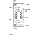
- FIGS. 17 to 20 are views showing the structure of a semiconductor device provided with a CFET
- FIG. 17 is a sectional view in the X direction
- FIG. 18 is a sectional view of a gate portion in the Y direction
- FIG. 19 is a source / drain in the Y direction.
- a cross-sectional view of the portion, FIG. 20 is a plan view.
- the X direction is the direction in which the nanowires extend
- the Y direction is the direction in which the gate extends
- the Z direction is the direction perpendicular to the substrate surface.
- FIGS. 17 to 20 are schematic views, and the dimensions and positions of the respective parts are not necessarily consistent.
- an element separation region 302 is formed on the surface of a semiconductor substrate 301 such as a silicon (Si) substrate, and the element active region 30a is defined by the element separation region 302.
- a semiconductor substrate 301 such as a silicon (Si) substrate
- the element active region 30a is defined by the element separation region 302.
- an N-type FET is formed on the P-type FET.
- a laminated transistor structure 390a is formed on the semiconductor substrate 301.
- the laminated transistor structure 390a includes a gate structure 391 formed on the semiconductor substrate 301.
- the gate structure 391 includes a gate electrode 356, a plurality of nanowires 358, a gate insulating film 355, and an insulating film 357.
- the gate electrode 356 extends in the Y direction and rises in the Z direction.
- the nanowires 358 penetrate the gate electrode 356 in the X direction and are arranged in the Y and Z directions.
- the gate insulating film 355 is formed between the gate electrode 356 and the nanowire 358.
- the gate electrode 356 and the gate insulating film 355 are formed at positions recessed from both ends of the nanowire 358 in the X direction, and the insulating film 357 is formed at the recessed portions.
- Insulating films 316 are formed on the semiconductor substrate 301 on both sides of the insulating film 357.
- Reference numerals 321 and 322 are interlayer insulating films.
- the gate electrode 356 is connected to the upper layer wiring by the via 385 provided in the opening 375.
- titanium, titanium nitride, polycrystalline silicon, or the like can be used for the gate electrode 356.
- a high dielectric constant material such as hafnium oxide, aluminum oxide, or oxides of hafnium and aluminum can be used for the gate insulating film 355.
- silicon or the like can be used for the nanowire 358.
- silicon oxide, silicon nitride, or the like can be used for the insulating film 316 and the insulating film 357.
- the number of nanowires 358 arranged in the Z direction is 4, and in the element active region 30a, a P-type semiconductor layer 331p is formed at each end of the two nanowires 358 on the semiconductor substrate 301 side. ..
- Two local wirings 386 in contact with the P-type semiconductor layer 331p are formed so as to sandwich the gate structure 391 in the X direction.
- an N-type semiconductor layer 341n is formed at each end of the two nanowires 358 on the side separated from the semiconductor substrate 101.
- Two local wirings 388 in contact with the N-type semiconductor layer 341n are formed so as to sandwich the gate structure 391 in the X direction.
- An insulating film 332 is formed between the local wiring 386 and the local wiring 388.
- An insulating film 389 is formed on the local wiring 388.
- the P-type semiconductor layer 331p is a P-type SiGe layer
- the N-type semiconductor layer 341n is an n-type Si layer.
- silicon oxide, silicon nitride, or the like can be used for the insulating film 332.
- the local wiring 388 is connected to the embedded wiring 3101 via the via 3071.
- the local wiring 386 is connected to the embedded wiring 3102 via the via 3072.
- the laminated transistor structure 390a has a P-type FET including a gate electrode 356, nanowires 358, a gate insulating film 355, and a P-type semiconductor layer 331p.
- a P-type FET including a gate electrode 356, nanowires 358, a gate insulating film 355, and a P-type semiconductor layer 331p.
- one P-type semiconductor layer 331p functions as a source region
- the other P-type semiconductor layer 331p functions as a drain region
- nanowire 358 functions as a channel.
- the laminated transistor structure 390a also has an N-type FET including a gate electrode 356, nanowires 358, a gate insulating film 355, and an N-type semiconductor layer 341n.
- one N-type semiconductor layer 341n functions as a source region
- the other N-type semiconductor layer 341n functions as a drain region
- nanowire 358 functions as a channel.
- wiring between transistors is performed by vias and metal wiring, but these can be realized by a known wiring process.
- the number of nanowires in the P-type FET and the N-type FET is assumed to be four in the Y direction and two in the Z direction, respectively, for a total of eight, but the number of nanowires is limited to this. It is not something that can be done. Further, the number of nanowires of the P-type FET and the N-type FET may be different.
- the semiconductor layer portion formed at both ends of the nanowire and forming the terminal serving as the source or drain of the transistor is referred to as a "pad".
- the P-type semiconductor layer 331p and the N-type semiconductor layer 341n correspond to pads.
- each insulating film and the like may be omitted.
- the nanowires and the pads on both sides thereof may be described in a simplified linear shape.
- expressions such as "same size” and the like that mean that the sizes and the like are the same include a range of manufacturing variation.
- the source and drain of the transistor are appropriately referred to as "nodes" of the transistor. That is, one node of the transistor refers to the source or drain of the transistor, and both nodes of the transistor refer to the source and drain of the transistor.
- the P-type FET and the N-type FET are basically laminated, but in some cases, the P-type FET or the N-type FET is formed only in the upper layer (or lower layer). ..
- the forming method for example, after forming the upper layer (or lower layer) device, the upper layer (or lower layer) device is partially removed (for example, the removal of the pad portion or the removal of the gate wiring and the pad portion). As a result, a P-type FET or an N-type FET can be formed only in the upper layer (or lower layer).
- the pad portion of the upper layer (or lower layer) device is formed by epitaxial growth, the upper layer (or lower layer) is partially non-formed, so that the P-type FET or the N-type FET is provided only in the upper layer (or lower layer). Can be formed.
- a P-type FET and an N-type FET are basically laminated, but in some cases, the same conductive type FET (P-type FET or N-type FET) is formed in the upper layer and the lower layer. Are laminated. That is, different conductive FETs may be formed in at least one of the upper layer and the lower layer.
- P-type FET or N-type FET conductive type FET
- different conductive FETs may be formed in at least one of the upper layer and the lower layer.
- VDD voltage or the power supply itself.
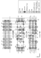
- FIGS. 1 (a), (b) and 2 (c) are plan views
- FIGS. (B) and (c) are cross-sectional views in the horizontal direction in a plan view.
- FIG. 1A shows a portion including a three-dimensional structure transistor formed in the lower part, that is, a side close to the substrate
- FIG. 1B shows a three-dimensional structure formed in the upper part, that is, a side far from the substrate.
- FIG. 1 (c) shows M1 and M2 layers which are metal wiring layers.
- FIG. 2A is a cross section of X1-X1'
- FIG. 2B is a cross section of X2-X2'
- FIG. 2C is a cross section of X3-X3'.
- FIG. 3 is a circuit diagram showing the configuration of the 2-port SRAM cell according to the first embodiment.
- the 2-port SRAM cell according to the present embodiment includes a 2-port SRAM circuit composed of load transistors PU1 and PU2, drive transistors PD1 and PD2, and access transistors PG1 to PG4. ing.
- the load transistors PU1 and PU2 are P-type FETs
- the drive transistors PD1 and PD2 and the access transistors PG1 to PG4 are N-type FETs.
- the load transistor PU1 is provided between the power supply VDD and the first node NA, and the drive transistor PD1 is provided between the first node NA and the power supply VSS.
- the gate of the load transistor PU1 and the drive transistor PD1 is connected to the second node NB, and constitutes the inverter INV1.
- the load transistor PU2 is provided between the power supply VDD and the second node NB, and the drive transistor PD2 is provided between the second node NB and the power supply VSS.
- the gate of the load transistor PU2 and the drive transistor PD2 is connected to the first node NA, and constitutes an inverter INV2. That is, the output of one inverter is connected to the input of the other inverter, thereby forming a latch.
- the access transistor PG1 is provided between the first bit line BLA and the first node NA, and the gate is connected to the first word line WLA.
- the access transistor PG2 is provided between the second bit line BLAX and the second node NB, and the gate is connected to the first word line WLA.
- the access transistor PG3 is provided between the third bit line BLB and the first node NA, and the gate is connected to the second word line WLB.
- the access transistor PG4 is provided between the 4th bit line BLBX and the 2nd node NB, and the gate is connected to the 2nd word line WLB.
- the first and second bit lines BLA and BLAX form a first complementary bit line pair
- the third and fourth bit lines BLB and BLBX form a second complementary bit line pair.
- the first and second bit lines BLA and BLAX constituting the first complementary bit line pair are driven to high level and low level, respectively, and the first word line WLA is driven to high level
- the high level is written to the first node NA and the low level is written to the second node NB.
- the first and second bit lines BLA and BLAX are driven to low level and high level, respectively, and the first word line WLA is driven to high level
- the low level is written to the first node NA and the second node.
- High level is written to NB.
- the latch state is determined and the first and second nodes NA and NB are set. The written data is retained.
- the first and second bit lines BLA and BLAX are precharged to a high level in advance and the first word line WLA is driven to a high level
- the data written to the first and second nodes NA and NB is displayed. Since the states of the first and second bit lines BLA and BLAX are determined accordingly, data can be read from the SRAM cell. Specifically, if the first node NA is at a high level and the second node NB is at a low level, the first bit line BLA holds the high level and the second bit line BLAX is discharged to the low level. On the other hand, if the first node NA is at a low level and the second node NB is at a high level, the first bit line BLA is discharged to the low level and the second bit line BLAX holds the high level.
- the third and fourth bit lines BLB and BLBX constituting the second complementary bit line pair are driven to the high level and the low level, respectively, and the second word line WLB is driven to the high level, the first node NA is reached.
- the high level is written and the low level is written to the second node NB.
- the 3rd and 4th bit lines BLB and BLBX are driven to low level and high level, respectively, and the 2nd word line WLB is driven to high level
- the low level is written to the 1st node NA and the 2nd node.
- the high level is written to NB.
- the latch state is determined and the first and second nodes NA and NB are set. The written data is retained.
- the 3rd and 4th bit lines BLB and BLBX are precharged to a high level in advance and the 2nd word line WLB is driven to a high level
- the data written to the 1st and 2nd nodes NA and NB is displayed. Since the states of the third and fourth bit lines BLB and BLBX are determined accordingly, data can be read from the SRAM cell. Specifically, if the first node NA is at a high level and the second node NB is at a low level, the third bit line BLB holds the high level and the fourth bit line BLBX is discharged to the low level. On the other hand, if the first node NA is low level and the second node NB is high level, the third bit line BLB is discharged to the low level and the fourth bit line BLBX holds the high level.
- the 2-port SRAM cell controls the first and second bit line BLA, BLAX, and the first word line WLA to write data to the SRAM cell, retain data, and the SRAM cell. It has a function to read data from. Further, the 2-port SRAM cell has a function of writing data to the SRAM cell, holding data, and reading data from the SRAM cell by controlling the 3rd and 4th bit lines BLB, BLBX, and the 2nd word line WLB. Has.
- the horizontal direction of the drawing is the X direction
- the vertical direction of the drawing is the Y direction
- the direction perpendicular to the substrate surface is the Z direction.
- the solid line running vertically and horizontally in the plan view of FIG. 1 and the like and the solid line running vertically and horizontally in the cross-sectional view of FIG. 2 and the like indicate a grid used for arranging parts at the time of design.
- the grids are evenly spaced in the X direction and evenly spaced in the Y direction.
- the grid spacing may be the same or different in the X direction and the Y direction. Further, the grid spacing may be different for each layer.
- each component does not necessarily have to be placed on the grid. However, from the viewpoint of suppressing manufacturing variations, it is preferable that the parts are arranged on the grid.
- the dotted line displayed so as to surround the cell in the plan view of FIG. 1 or the like indicates the cell frame of the 2-port SRAM cell (the outer edge of the 2-port SRAM cell).
- the 2-port SRAM cell is arranged so that the cell frame is in contact with the cell frame of the adjacent cell in the X direction or the Y direction.
- power supply wirings 11 and 12 extending in the Y direction are provided at the lower part of the cell, respectively.
- Both the power supply wirings 11 and 12 are embedded power supply wirings (BPR: Buried Power Rail) formed in the embedded wiring layer.
- the power supply wirings 11 and 12 each supply a voltage VSS.
- transistors P1 and P2 correspond to load transistors PU2 and PU1, respectively.
- Transistors N1 and N5 correspond to drive transistor PD1.
- Transistors N2 and N6 correspond to drive transistor PD2.
- Transistors N3, N4, N7, and N8 correspond to access transistors PG1 to PG4, respectively.
- Nanowires 21a to 21c and 26a to 26d extending in the Y direction are formed in the lower part of the cell, and nanowires 21d to 21j extending in the Y direction are formed in the upper part of the cell.
- the nanowires 21a, 26a, 26c are formed side by side in the X direction.
- the nanowires 21b, 21c, 26b, 26d are formed side by side in the X direction.
- the nanowires 21d, 21f, 21g, and 21i are formed side by side in the X direction.
- the nanowires 21e, 21h, 21j are formed side by side in the X direction.
- the nanowires 21d, 21i, 26a and 26c are formed side by side with the nanowires 21e, 21j, 26b and 26d in the Y direction, respectively. Further, the nanowires 21b and 21g are formed at the same position in the X direction in a plan view.
- nanowires 21a, 21c, 26a to 26d overlap with the nanowires 21f, 21h, 21d, 21e, 21i, 21j in a plan view, respectively.
- the gate wirings (Gates) 31 to 36 extend in the Z direction and extend in the X direction from the lower part of the cell to the upper part of the cell.
- the gate wirings 31 to 33 are formed side by side in the X direction, and the gate wirings 34 to 36 are formed side by side in the X direction.
- the gate wiring 31 serves as a gate for the transistor N3 and the dummy transistor N21.
- the gate wiring 32 serves as a gate for the transistors N1, N5, and P2.
- the gate wiring 33 serves as a gate for the transistor N7 and the dummy transistor N23.
- the gate wiring 34 serves as a gate for the transistor N4 and the dummy transistor N22.
- the gate wiring 35 serves as a gate for transistors N2, N6, and P1.
- the gate wiring 36 serves as a gate for the transistor N8 and the dummy transistor N24.
- the nanowires 21a, 21c, 21d to 21f, 21h to 21j form the channel portions of the transistors N1 to N8, respectively.
- the pads 22a and 22b form a node of the transistor N1.
- the pads 22c and 22d form a node of the transistor N2.
- the pads 22e and 22f form a node of the transistor N3.
- the pads 22f and 22g form a node of the transistor N4.
- the pads 22h and 22i form a node of the transistor N5.
- the pads 22j and 22k form a node of the transistor N6.
- the pads 22l and 22m form a node of the transistor N7.
- the pads 22m and 22n form a node of the transistor N8.
- the transistor N1 is composed of the nanowires 21a, the gate wiring 32, and the pads 22a and 22b.
- the transistor N2 is composed of nanowires 21c, gate wiring 35, and pads 22c and 22d.
- the transistor N3 is composed of nanowires 21d, gate wiring 31, and pads 22e and 22f.
- the transistor N4 is composed of nanowires 21e, gate wiring 34, and pads 22f, 22g.
- the transistor N5 is composed of nanowires 21f, gate wiring 32, and pads 22h and 22i.
- the transistor N6 is composed of nanowires 21h, gate wiring 35, and pads 22j and 22k.
- the transistor N7 is composed of nanowires 21i, gate wiring 33, and pads 22l and 22m.
- the transistor N8 is composed of nanowires 21j, gate wiring 36, and pads 22m and 22n.
- Pads 22o to 22r doped with a P-type semiconductor are formed at the upper end of the drawing of the nanowire 21b, the lower end of the drawing of the nanowire 21b, the upper end of the drawing of the nanowire 21g, and the lower end of the drawing of the nanowire 21g, respectively.
- Nanowires 21b and 21g form channel portions of transistors P1 and P2, respectively.
- the pads 22o and 22p form the node of the transistor P1.
- the pads 22q and 22r form a node of the transistor P2.
- the transistor P1 is composed of the nanowire 21b, the gate wiring 35, and the pads 22o and 22p.
- the transistor P2 is composed of 21 g of nanowires, gate wiring 32, and pads 22q and 22r.
- 27f are formed respectively.
- the dummy pads 27a and 27b form a node of the dummy transistor N21.
- the dummy pads 27b and 27c form a node of the dummy transistor N22.
- the dummy pads 27d and 27e form a node of the dummy transistor N23.
- the dummy pads 27e and 27f form a node of the dummy transistor N24.
- the nanowires 26a to 26d correspond to the channel portions of the dummy transistors N21 to N24.
- the dummy transistors N21 to N24 are transistors that do not have a logic function. Further, in the circuit diagram of FIG. 3, the dummy transistors N21 to N24 are omitted. Although some of the 2-port SRAM cells in the embodiments and modifications described below include dummy transistors, each dummy transistor does not affect the logical function of the 2-port SRAM cell. Is omitted.
- the transistors N3 to N8 overlap with the dummy transistors N21 and N22, the transistors N1 and N2, and the dummy transistors N23 and N24, respectively, in a plan view.
- the transistors N1 and the dummy transistors N21 and N23 are formed side by side in the X direction.
- the transistors N2 and P1 and the dummy transistors N22 and N24 are formed side by side in the X direction.
- the transistors N3, N5, N7, and P2 are formed side by side in the X direction.
- the transistors N4, N6, and N8 are formed side by side in the X direction.
- the transistors N3 and N7 and the dummy transistors N21 and N23 are formed side by side with the transistors N4 and N8 and the dummy transistors N22 and N24, respectively, in the Y direction. Further, the transistors P1 and P2 are formed at the same positions in the X direction in a plan view.
- Local wiring (LI: Local Interconnect) 41a to 41e extending in the X direction is formed at the bottom of the cell.
- the local wiring 41a is connected to the pad 22a.
- the local wiring 41b is connected to the pad 22b.
- the local wiring 41c is connected to the pads 22c and 22o.
- the local wiring 41d is connected to the pad 22p.
- the local wiring 41e is connected to the pad 22d.
- Local wiring 41f to 41n extending in the X direction is formed on the upper part of the cell.
- the local wiring 41f is connected to the pad 22e.
- the local wiring 41g is connected to the pad 22h.
- the local wiring 41h is connected to the pad 22q.
- the local wiring 41i is connected to the pad 22l.
- the local wiring 41j is connected to the pads 22f, 22i, 22r.
- the local wiring 41k is connected to the pads 22j and 22m.
- the local wiring 41l is connected to the pad 22g.
- the local wiring 41m is connected to the pad 22k.
- the local wiring 41n is connected to the pad 22n.
- the local wiring 41a is connected to the power supply wiring 11 via the contact (via) 51a, and is connected to the local wiring 41g via the contact 51b.
- the local wiring 41b is connected to the local wiring 41j via the contact 51c.
- the local wiring 41c is connected to the local wiring 41k via the contact 51d.
- the local wiring 41e is connected to the power supply wiring 12 via the contact 51e, and is connected to the local wiring 41m via the contact 51f.
- the local wiring 41j is connected to the gate wiring 35 via the shared-contact 61a.
- the local wiring 41k is connected to the gate wiring 32 via the shared contact 61b.
- the pads of the transistors N1 and N5 are connected to each other by local wiring and contacts, and share the gate wiring.
- the pads of the transistors N2 and N6 are connected to each other by local wiring and contacts, and share the gate wiring.
- the transistors N1 and N5 correspond to the drive transistor PD1
- the transistors N2 and N6 correspond to the drive transistor PD2. Therefore, in the 2-port SRAM cell according to the present embodiment, the drive transistors PD1 and PD2 are each composed of two N-type FETs connected in parallel.
- the local wiring 41b, 41j, contact 51c, shared contact 61a, and gate wiring 35 correspond to the first node NA
- the local wiring 41c, 41k, contact 51d, shared contact 61b, and gate wiring 32 correspond to the second node NB. To do.
- wirings 71 to 75 extending in the Y direction are formed in the M1 wiring layer, which is a metal wiring layer, from both the upper and lower ends of the cell. Further, wirings 76 to 79 are formed.
- the wiring 71 supplies the voltage VDD.
- Wiring 72 to 75 correspond to the first bit line BLA, the third bit line BLB, the second bit line BLAX, and the fourth bit line BLBX, respectively.
- Wiring 81, 82 extending in the X direction is formed on the M2 wiring layer, which is the upper layer of the M1 wiring layer, from both the left and right ends of the cell.
- the wirings 81 and 82 are arranged side by side in the Y direction.
- the wirings 81 and 82 correspond to the first word line WLA and the second word line WLB, respectively.
- the wiring 71 is connected to the local wiring 41h via the contact 91a, and is connected to the local wiring 41d via the contact 91b.
- the wiring 72 is connected to the local wiring 41f via the contact 91c.
- the wiring 73 is connected to the local wiring 41l via the contact 91d.
- the wiring 74 is connected to the local wiring 41i via the contact 91e.
- the wiring 75 is connected to the local wiring 41n via the contact 91f.
- the wiring 76 is connected to the gate wiring 31 via the contact (Gate-contact) 61c, and is connected to the wiring 81 via the contact 91g.
- the wiring 77 is connected to the gate wiring 33 via the contact 61d, and is connected to the wiring 81 via the contact 91h.
- the wiring 78 is connected to the gate wiring 34 via the contact 61e, and is connected to the wiring 82 via the contact 91i.
- the wiring 79 is connected to the gate wiring 36 via the contact 61f, and is connected to the wiring 82 via the contact 91j.
- the wiring 81 is connected to the gate wiring 31 via the contact 91g, the wiring 76, and the contact 61c, and is connected to the gate wiring 33 via the contact 91h, the wiring 77, and the contact 61d.
- the wiring 82 is connected to the gate wiring 34 via the contact 91i, the wiring 78, and the contact 61e, and is connected to the gate wiring 36 via the contact 91j, the wiring 79, and the contact 61f.
- the pad 22q is connected to the wiring 71 that supplies the voltage VDD
- the pad 22r is connected to the local wiring 41j (first node NA)
- the gate wiring 32 is the shared contact 61b (second). It is connected to each node NB).
- the pad 22p is connected to the wiring 71 that supplies the voltage VDD
- the pad 22o is connected to the local wiring 41c (second node NB)
- the gate wiring 35 is connected to the shared contact 61a (first node NA). It is connected.
- the pads 22b and 22i are in local wiring 41b and 41j (first node NA), the pads 22a and 22h are in power supply wiring 11 for supplying voltage VSS, and the gate wiring 32 is in shared contact. They are connected to 61b (second node NB), respectively.
- the pads 22c and 22j make local wiring 41c and 41k (second node NB), the pads 22d and 22k supply voltage VSS to the power supply wiring 12, and the gate wiring 35 makes shared contact. It is connected to each of 61a (first node NA).
- the pad 22e is connected to the wiring 72 (first bit line BLA)
- the pad 22f is connected to the local wiring 41j (first node NA)
- the gate wiring 31 is connected to the wiring 81 (first word line WLA).
- the pad 22l is connected to the wiring 74 (second bit line BLAX)
- the pad 22m is connected to the local wiring 41k (second node NB)
- the gate wiring 33 is connected to the wiring 81 (first word line WLA).
- the pad 22g is connected to the wiring 73 (third bit line BLB), the pad 22f is connected to the local wiring 41j (first node NA), and the gate wiring 34 is connected to the wiring 82 (second word line WLB).
- the pad 22n is connected to the wiring 75 (4th bit line BLBX)
- the pad 22m is connected to the local wiring 41k (second node NB)
- the gate wiring 36 is connected to the wiring 82 (second word line WLB).
- a 2-port SRAM circuit is composed of transistors N1 to N8, P1 and P2.
- transistors N1, N2 and P1 are formed in the lower part of the cell, and transistors N3 to N8 and P2 are formed in the upper part of the cell.
- the transistors N1 to N8, P1 and P2 are three-dimensional structure transistors, respectively. As a result, a 2-port SRAM cell using a CFET can be realized.
- the transistors P1 and P2 are formed at the same position in the X direction in a plan view. As a result, the area of the 2-port SRAM cell can be reduced.
- the drive transistor PD1 is composed of transistors N1 and N5 connected in parallel
- the drive transistor PD2 is composed of transistors N2 and N6 connected in parallel.
- the transistors N1 and N2 overlap with the transistors N5 and N6 in a plan view, respectively. As a result, the area can be reduced while improving the driving capacity of the 2-port SRAM cell.
- the 2-port SRAM cells When the 2-port SRAM cells are arranged adjacent to each other in the X direction, they may be arranged by inverting them in the X direction or they may be arranged without inverting them in the X direction. Further, when the 2-port SRAM cells are arranged adjacent to each other in the Y direction, they are arranged so as to be inverted in the Y direction.
- the dummy transistors N21 to N24 do not affect the logic function of the 2-port SRAM cell. Further, although the dummy transistors N21 to N24 may not be formed, it is possible to suppress the manufacturing variation of the semiconductor storage device, improve the yield, and improve the reliability by forming the dummy transistors N21 to N24. ..
- the shared contact 61a connecting the local wiring 41j and the gate wiring 35 and the shared contact 61b connecting the local wiring 41k and the gate wiring 32 connect the wiring arranged in the M1 wiring layer and the gate wiring.
- the contacts 61c to 61f may be formed in the same process step, or may be formed in another process step.
- the wiring 71 for supplying the voltage VDD is provided in the M1 wiring layer
- the wiring for supplying the voltage VDD may be provided in the embedded wiring layer.
- wiring for supplying the voltage VDD may be provided in both the M1 wiring layer and the embedded wiring layer. In this case, since the power supply for supplying the voltage VDD is strengthened, the power supply can be stabilized.
- the transistors N3, N4, N7 and N8 are formed in the upper part of the cell, the transistors N3, N4, N7 and N8 may be formed in the lower part of the cell. In this case, the transistors N3, N4, N7, and N8 are formed in the lower part of the cell instead of the dummy transistors N21 to N24. Then, local wiring and contacts are formed in the 2-port SRAM cell so that the above-mentioned 2-port SRAM circuit is formed.
- FIG. 4 is a plan view showing another example of the layout structure of the 2-port SRAM cell according to the first embodiment. Specifically, FIG. 4A shows the lower part of the cell, FIG. 4B shows the upper part of the cell, and FIG. 4C shows the M1 and M2 wiring layers.
- transistors N11 to N14, N17, and N18 are formed in the lower part of the cell in addition to transistors N1, N2, and P1, and dummy transistors N21 to N24 are omitted. Further, in addition to the transistors N3 to N8 and P2, the transistors N15 and N16 are formed on the upper part of the cell.
- nanowires 23a, 23c, 23d, 23e, 23i, 23j extending in the Y direction are formed in the lower part of the cell, and nanowires 23f, 23h extending in the Y direction are formed in the upper part of the cell.
- the nanowires 23a, 23d, 23i are formed side by side with the nanowires 21a in the X direction.
- the nanowires 23c, 23e, 23j are formed side by side with the nanowires 21b, 21c in the X direction.
- the nanowires 23f are formed side by side with the nanowires 21d, 21f, 21g, 21i in the X direction.
- the nanowires 23h are formed side by side with the nanowires 21e, 21h, 21j in the X direction.
- nanowires 23d and 23i are formed side by side with the nanowires 23e and 23j in the Y direction, respectively.
- nanowires 23a, 23c, 23d, 23e, 23i, 23j overlap with the nanowires 23f, 23h, 21d, 21e, 21i, 21j in a plan view, respectively.
- the gate wiring 31 serves as the gate of the transistor N13.
- the gate wiring 32 serves as a gate for the transistors N11 and N15.
- the gate wiring 33 serves as a gate for the transistor N17.
- the gate wiring 34 serves as a gate for the transistor N14.
- the gate wiring 35 serves as a gate for the transistors N12 and N16.
- the gate wiring 36 serves as a gate for the transistor N18.
- Nanowires 23a, 23c, 23d, 23e, 23f, 23h, 23i, 23j form a channel portion of transistors N11 to N18.
- the pads 24a and 24b form a node of the transistor N11.
- the pads 24c and 24d form a node of the transistor N12.
- the pads 24e and 24f form a node of the transistor N13.
- the pads 24f and 24g form a node of the transistor N14.
- the pads 24h and 24i form a node of the transistor N15.
- the pads 24j and 24k form a node of the transistor N16.
- the pads 24l and 24m form a node of the transistor N17.
- the pads 24m and 24n form a node of the transistor N18.
- the transistor N11 is composed of the nanowires 23a, the gate wiring 32, and the pads 24a and 24b.
- the transistor N12 is composed of nanowires 23c, gate wiring 35, and pads 24c, 24d.
- the transistor N13 is composed of nanowires 23d, gate wiring 31, and pads 24e and 24f.
- the transistor N14 is composed of nanowires 23e, gate wiring 34, and pads 24f, 24g.
- the transistor N15 is composed of nanowires 23f, gate wiring 32, and pads 24h and 24i.
- the transistor N16 is composed of nanowires 23h, gate wiring 35, and pads 24j and 24k.
- the transistor N17 is composed of nanowires 23i, gate wiring 33, and pads 24l, 24m.
- the transistor N18 is composed of nanowires 23j, gate wiring 36, and pads 24m and 24n.
- the transistors N11 to N14, N17, and N18 overlap with the transistors N15, N16, N3, N4, N7, and N8 in a plan view, respectively.
- the transistors N11, N13, and N17 are formed side by side with the transistors N1 in the X direction.
- the transistors N12, N14, and N18 are formed side by side with the transistors N2 and P1 in the X direction.
- the transistor N15 is formed side by side with the transistors N3, N5, N7, and P2 in the X direction.
- the transistor N16 is formed side by side with the transistors N4, N6, and N8 in the X direction.
- the transistors N13 and N17 are formed side by side with the transistors N14 and N18 in the Y direction, respectively.
- Local wirings 42a to 42d extending in the X direction are formed at the bottom of the cell.
- the local wiring 42a is connected to the pad 24e.
- the local wiring 42b is connected to the pad 24l.
- the local wiring 42c is connected to the pad 24g.
- the local wiring 42d is connected to the pad 24n.
- the local wiring 41a is connected to the pads 22a and 24a.
- the local wiring 41b is connected to the pads 22b, 24b, 24f.
- the local wiring 41c is connected to the pads 22c, 22o, 24c, 24m.
- the local wiring 41e is connected to the pads 22d and 24d.
- the local wiring 41g is connected to the pads 22h and 24h.
- the local wiring 41j is connected to the pads 22f, 22i, 24i.
- the local wiring 41k is connected to the pads 22j, 22m, 22r, 24j.
- the local wiring 41m is connected to the pads 22k and 24k.
- the local wiring 42a is connected to the local wiring 41f via the contact 52a.
- the local wiring 42b is connected to the local wiring 41i via the contact 52b.
- the local wiring 42c is connected to the local wiring 41l via the contact 52c.
- the local wiring 42d is connected to the local wiring 41n via the contact 52d.
- the pads of each other are connected by local wiring and contacts, and share the gate wiring.
- the pads of each other are connected by local wiring and contacts, and share the gate wiring.
- the pads of the transistors N3 and N13 are connected to each other by local wiring and contacts, and share the gate wiring.
- the pads of the transistors N4 and N14 are connected to each other by local wiring and contacts, and share the gate wiring.
- the pads of the transistors N7 and N17 are connected to each other by local wiring and contacts, and share the gate wiring.
- the pads of the transistors N8 and N18 are connected to each other by local wiring and contacts, and share the gate wiring.
- the transistors N1, N5, N11, and N15 correspond to the drive transistor PD1
- the transistors N2, N6, N12, and N16 correspond to the drive transistor PD2
- the transistors N3 and N13 correspond to the access transistor PG1.
- Transistors N7 and N17 correspond to access transistor PG2
- transistors N4 and N14 correspond to access transistor PG3
- transistors N8 and N18 correspond to access transistor PG4.
- the drive transistors PD1 and PD2 are each composed of four N-type FETs connected in parallel, and the access transistors PG1 to PG4 are each composed of two N-type FETs connected in parallel. ing. Further, the transistors corresponding to the drive transistors PD1 and PD2 and the transistors corresponding to the access transistors PG1 to PG4 are laminated. Then, according to this modification, the same effect as that of the 2-port SRAM cell according to the first embodiment can be obtained.
- the drive transistor PD1 is composed of transistors N1, N5, N11 and N15 connected in parallel
- the drive transistor PD2 is composed of transistors N2, N6, N12 and N16 connected in parallel
- the access transistor PG1 is in parallel.
- the access transistor PG2 is composed of the connected transistors N3 and N13
- the access transistor PG2 is composed of the transistors N7 and N17 connected in parallel
- the access transistor PG3 is composed of the transistors N4 and N14 connected in parallel
- the access transistor PG4 is composed of the transistors N4 and N14 connected in parallel. It is composed of transistors N8 and N18 connected in parallel.
- the transistors N11 to N14, N17, and N18 overlap with the transistors N15, N16, N3, N4, N7, and N8 in a plan view, respectively. As a result, the area can be reduced while improving the driving capacity of the 2-port SRAM cell.
- FIG. 5 is a plan view showing another example of the layout structure of the 2-port SRAM cell according to the first embodiment. Specifically, FIG. 5A shows the lower part of the cell, FIG. 5B shows the upper part of the cell, and FIG. 5C shows the M1 and M2 wiring layers. In FIG. 5, in comparison with FIG. 1, the transistor P1 is formed in the upper part of the cell. Further, dummy transistors N25 and N26 are formed in the lower part of the cell.
- nanowires 21b are formed on the upper part of the cell.
- Nanowires 28a and 28b extending in the Y direction are formed in the lower part of the cell.
- the nanowires 21b are formed side by side with the nanowires 21e, 21h, 21j in the X direction.
- the nanowires 28a are formed side by side with the nanowires 21a, 26a, 26c in the X direction.
- the nanowires 28b are formed side by side with the nanowires 21c, 26b, 26d in the X direction.
- nanowires 21g and 21b overlap with the nanowires 28a and 28b in a plan view, respectively.
- N-type semiconductor-doped dummy pads 29a to 29d are formed at the upper end of the drawing of the nanowire 28a, the lower end of the drawing of the nanowire 28a, the upper end of the drawing of the nanowire 28b, and the lower end of the drawing of the nanowire 28b.
- the nanowires 28a and 28b form channel portions of the dummy transistors N25 and N26, respectively.
- the dummy pads 29a and 29b form a node of the dummy transistor N25, and the dummy pads 29c and 29d form a node of the dummy transistor N26.
- the dummy transistors N25 and N26 are transistors having no logic function.
- the transistors P2 and P1 overlap with the dummy transistors N25 and N26 in a plan view, respectively.
- the transistor P1 is formed side by side with the transistors N4, N6, N8 in the X direction.
- the dummy transistor N25 is formed side by side with the transistor N1 and the dummy transistors N21 and N23 in the X direction.
- the dummy transistor N26 is formed side by side with the transistor N2 and the dummy transistors N22 and N24 in the X direction.
- the local wiring 41c is connected to the pad 22c.
- the local wiring 41k is connected to the pads 22o, 22j, 22m.
- each transistor including the dummy transistor is stacked. Further, the transistor including the dummy transistor formed in the lower part of the cell is only an N-type FET. Then, according to this modification, the same effect as that of the 2-port SRAM cell according to the first embodiment can be obtained.
- the transistors N3 to N8, P2 and P1 overlap with the dummy transistors N21 and N22, the transistors N1 and N2 and the dummy transistors N23 to N26 in a plan view, respectively. That is, each transistor including the dummy transistor is laminated with other transistors. As a result, it is not necessary to remove some of the transistors, so that the complexity of the manufacturing process can be suppressed.
- transistors N1 and N2 and dummy transistors N21 to N26 are formed in the lower part of the cell, and transistors P1, P2 and N3 to N8 are formed in the upper part of the cell. That is, only the N-type FET is arranged in the lower part of the cell, and the above configuration can be realized by replacing a part of the transistors arranged in the upper part of the cell with the N-type FET. As a result, the complexity of the manufacturing process can be suppressed.
- FIG. 6 is a plan view showing another example of the layout structure of the 2-port SRAM cell according to the first embodiment. Specifically, FIG. 6A shows the lower part of the cell, FIG. 6B shows the upper part of the cell, and FIG. 6C shows the M1 and M2 wiring layers.
- FIG. 6 in comparison with FIG. 1, in addition to the transistors N1 and N2, the transistors N11 to N14, N17, N18 and the dummy transistors N25 and N26 are formed in the lower part of the cell, and the dummy transistors N21 to N24 are omitted. ing. Further, in addition to the transistors N3 to N8 and P2, the transistors N15, N16 and P1 are formed on the upper part of the cell.
- Local wirings 42a to 42d are formed at the bottom of the cell. At the top of the cell, the local wiring 41j is connected to the pads 22f, 22i, 22r, 24i. The local wiring 41k is connected to the pads 22j, 22m, 22o, 24j.
- the transistors N1, N5, N11, and N15 correspond to the drive transistor PD1
- the transistors N2, N6, N12, and N16 correspond to the drive transistor PD2
- the transistors N3 and N13 correspond to the access transistor PG1.
- Transistors N7 and N17 correspond to access transistor PG2
- transistors N4 and N14 correspond to access transistor PG3
- transistors N8 and N18 correspond to access transistor PG4.
- the drive transistors PD1 and PD2 are each composed of four N-type FETs connected in parallel, and the access transistors PG1 to PG4 are each composed of two N-type FETs connected in parallel. It is configured. Further, each transistor including a dummy transistor is laminated. Further, the transistor including the dummy transistor formed in the lower part of the cell is only an N-type FET. Then, according to this modification, the same effect as that of the 2-port SRAM cell according to the first embodiment can be obtained.
- the drive transistor PD1 is composed of transistors N1, N5, N11 and N15 connected in parallel
- the drive transistor PD2 is composed of transistors N2, N6, N12 and N16 connected in parallel
- the access transistor PG1 is in parallel.
- the access transistor PG2 is composed of the connected transistors N3 and N13
- the access transistor PG2 is composed of the transistors N7 and N17 connected in parallel
- the access transistor PG3 is composed of the transistors N4 and N14 connected in parallel
- the access transistor PG4 is composed of the transistors N4 and N14 connected in parallel. It is composed of transistors N8 and N18 connected in parallel.
- the transistors N11 to N14, N17, and N18 overlap with the transistors N15, N16, N3, N4, N7, and N8 in a plan view, respectively. As a result, the area can be reduced while improving the driving capacity of the 2-port SRAM cell.
- the transistors N3 to N8, N15, N16, P1 and P2 overlap with the transistors N13, N14, N1, N2, N17, N18, N11, N12 and the dummy transistors N26 and N25, respectively, in a plan view. That is, each transistor including the dummy transistor is laminated with other transistors. As a result, it is not necessary to remove some of the transistors, so that the complexity of the manufacturing process can be suppressed.
- transistors N1, N2, N11 to N14, N17, N18 and dummy transistors N25 and N26 are formed in the lower part of the cell
- transistors N3 to N8, N15, N16, P1 and P2 are formed in the upper part of the cell.
- FIG. 7 is a plan view showing another example of the layout structure of the 2-port SRAM cell according to the first embodiment. Specifically, FIG. 7A shows the lower part of the cell, FIG. 7B shows the upper part of the cell, and FIG. 7C shows the M1 and M2 wiring layers.
- transistors N5 and N6 are formed in the lower part of the cell in addition to the transistors N1 and N2 and the dummy transistors N21 to N24. Further, in addition to the transistors N3, N4, N7, N8, and P2, the transistors P1 and the dummy transistors P21 and P22 are formed on the upper part of the cell.
- nanowires 21f and 21h are formed at the bottom of the cell.
- Nanowires 21b and nanowires 28c and 28d extending in the Y direction are formed on the upper part of the cell.
- the nanowires 21f are formed side by side with the nanowires 21a, 26a, 26c in the X direction.
- the nanowires 21h are formed side by side with the nanowires 21c, 26b, 26d in the X direction.
- the nanowires 28c are formed side by side with the nanowires 21d, 21g, 21i in the X direction.
- the nanowires 21b and 28d are formed side by side with the nanowires 21e and 21j in the X direction.
- nanowires 21a, 21f, 21c and 21h overlap with the nanowires 21g, 28c, 28d and 21b in a plan view, respectively.
- Dummy pads 29e to 29h doped with a P-type semiconductor are formed at the upper end of the drawing of the nanowire 28c, the lower end of the drawing of the nanowire 28c, the upper end of the drawing of the nanowire 28d, and the lower end of the drawing of the nanowire 28d, respectively.
- the nanowires 28c and 28d form the channel portions of the dummy transistors P21 and P22, respectively.
- the dummy pads 29e and 29f form a node of the dummy transistor P21, and the dummy pads 29g and 29h form a node of the dummy transistor P22.
- the dummy transistors P21 and P22 are transistors having no logic function.
- the transistors P1 and P2 and the dummy transistors P21 and P22 overlap with the transistors N6, N1, N5 and N2 in a plan view, respectively.
- the transistors N5 and N6 are formed side by side with the transistors N1 and N2 in the X direction, respectively.
- wirings 71a and 71b extending in the X direction are formed in the M1 wiring layer.
- the wirings 71a and 71b each supply a voltage VDD.
- the wiring 71a is connected to the local wiring 41h via the contact 91a.
- the wiring 71b is connected to the local wiring 41d via the contact 91b.
- transistors corresponding to drive transistors PD1 and PD2 are formed side by side in the X direction at the bottom of the cell. Further, a transistor corresponding to the load transistors PU1 and PU2 is formed on the upper part of the cell, and is laminated with a transistor corresponding to the drive transistors PD1 and PD2. Then, according to this modification, the same effect as that of the 2-port SRAM cell according to the first embodiment can be obtained.
- the transistors N1, N2, N5, N6 and the dummy transistors N21 to N24 overlap the transistors P2, the dummy transistors P22, P21 and the transistors P1, N3, N4, N7, N8 in a plan view, respectively. That is, each transistor including the dummy transistor is laminated with other transistors. As a result, it is not necessary to remove some of the transistors, so that the complexity of the manufacturing process can be suppressed.
- transistors N1, N2, N5, N6 and dummy transistors N21 to N24 are formed in the lower part of the cell
- transistors N3, N4, N7, N8, P1, P2 and dummy transistors P21, P22 are formed in the upper part of the cell. Is formed. That is, only the N-type FET is arranged in the lower part of the cell, and the above configuration can be realized by replacing a part of the transistors arranged in the upper part of the cell with the N-type FET. As a result, the complexity of the manufacturing process can be suppressed.
- FIG. 8 is a diagram showing an example of the layout structure of the 2-port SRAM cell according to the second embodiment. Specifically, FIG. 8A shows the lower part of the cell, FIG. 8B shows the upper part of the cell, and FIG. 8C shows the M1 and M2 wiring layers.
- transistors N1, N2, N7, N8, N47, N48, and P1 are formed in the lower part of the cell, and transistors N3 to N6, N43, N44, and P2 are formed in the upper part of the cell.
- another 2-port SRAM cell is arranged adjacent to the 2-port SRAM cell according to the present embodiment in the X direction.
- the transistors N43 and N44 are transistors included in the 2-port SRAM cell arranged on the right side of the drawing of the 2-port SRAM cell according to the present embodiment. Further, the transistors N47 and N48 are transistors included in the 2-port SRAM cell arranged on the left side of the drawing of the 2-port SRAM cell according to the present embodiment.
- nanowires 21i and 21j are formed at the bottom of the cell. Further, nanowires 121i and 121j extending in the Y direction are formed at the left end of the drawing at the lower part of the cell, and nanowires 121d and 121e extending in the Y direction are formed at the right end of the drawing at the upper part of the cell.
- the nanowires 121d are formed side by side with the nanowires 21d, 21f, 21g in the X direction.
- the nanowires 121e are formed side by side with the nanowires 21e and 21h in the X direction.
- the nanowires 121i are formed side by side with the nanowires 21a and 21i in the X direction.
- the nanowires 121j are formed side by side with the nanowires 21b, 21c, 21j in the X direction.
- nanowires 121d and 121e are formed side by side in the Y direction.
- the nanowires 121i and 121j are formed side by side in the Y direction.
- nanowires 121d, 121e, 121i, 121j overlap with the nanowires 21i, 21j, 21d, 21e in a plan view, respectively.
- the gate wiring 33 serves as the gate of the transistor N43.
- the gate wiring 36 serves as a gate for the transistor N44.
- the gate wiring 31 serves as a gate for the transistor N47.
- the gate wiring 34 serves as a gate for the transistor N48.
- the transistors N43 and N44 overlap with the transistors N7 and N8 in a plan view, respectively.
- the transistors N47 and N48 overlap with the transistors N3 and N4 in a plan view, respectively.
- the transistor N43 is formed side by side with the transistors N3, N5, P2 in the X direction.
- the transistor N44 is formed side by side with the transistors N4 and N6 in the X direction.
- the transistor N47 is formed side by side with the transistors N1 and N7 in the X direction.
- the transistor N48 is formed side by side with the transistors N2, N8, and P1 in the X direction.
- the transistors N43 and N44 are formed side by side in the Y direction.
- the transistors N47 and N48 are formed side by side in the Y direction.
- the local wiring 41c is connected to the pads 22c, 22m, 22o.
- the local wiring 41k is connected to the pad 22j.
- a 2-port SRAM circuit is configured by the transistors N1 to N8, P1 and P2. Further, transistors N1, N2, N7, N8, and P1 are formed in the lower part of the cell, and transistors N3 to N6 and P2 are formed in the upper part of the cell.
- the transistors N1 to N8, P1 and P2 are three-dimensional structure transistors, respectively. As a result, a 2-port SRAM cell using a CFET can be realized.
- the transistors P1 and P2 are formed at the same position in the X direction in a plan view. As a result, the area of the 2-port SRAM cell can be reduced.
- the drive transistor PD1 is composed of transistors N1 and N5 connected in parallel
- the drive transistor PD2 is composed of transistors N2 and N6 connected in parallel.
- the transistors N1 and N2 overlap with the transistors N5 and N6 in a plan view, respectively. As a result, the area can be reduced while improving the driving capacity of the 2-port SRAM cell.
- the transistors N43 and N44 correspond to the transistors N3 and N4 in the 2-port SRAM cell arranged on the right side of the drawing of the 2-port SRAM cell according to the present embodiment, respectively.
- the transistors N47 and N48 correspond to the transistors N7 and N8 in the 2-port SRAM cell arranged on the left side of the drawing of the 2-port SRAM cell according to the present embodiment, respectively.
- the transistors N43 and N44 overlap with the transistors N7 and N8 in a plan view
- the transistors N47 and N48 overlap with the transistors N3 and N4 in a plan view, respectively.
- the transistor N3 corresponding to the access transistor PG1 is laminated with the transistor N47 corresponding to the access transistor PG2 of the 2-port SRAM cell adjacent to the left side of the drawing.
- the transistor N7 corresponding to the access transistor PG2 is laminated with the transistor N43 corresponding to the access transistor PG1 of the 2-port SRAM cell adjacent to the right side of the drawing.
- the transistor N4 corresponding to the access transistor PG3 is laminated with the transistor N48 corresponding to the access transistor PG4 of the 2-port SRAM cell adjacent to the left side of the drawing.
- the transistor N8 corresponding to the access transistor PG4 is laminated with the transistor N44 corresponding to the access transistor PG3 of the 2-port SRAM cell adjacent to the right side of the drawing.
- the 2-port SRAM cells adjacent to each other in the X direction are arranged without being inverted in the X direction. Further, the 2-port SRAM cell and the 2-port SRAM cell adjacent to each other in the Y direction are arranged so as to be inverted in the Y direction.
- the transistors N3, N4, N43, N44 may be formed in the lower part of the cell, and the transistors N7, N8, N47, N48 may be formed in the upper part of the cell.
- local wiring and contacts are formed in the 2-port SRAM cell according to the present embodiment so that the 2-port SRAM cell circuit is formed.
- FIG. 9 is a diagram showing another example of the layout structure of the 2-port SRAM cell according to the second embodiment. Specifically, FIG. 9A shows the lower part of the cell, FIG. 9B shows the upper part of the cell, and FIG. 9C shows the M1 and M2 wiring layers. In FIG. 9, the transistor P1 is formed in the upper part of the cell in comparison with FIG. Further, dummy transistors N25 and N26 are formed in the lower part of the cell.
- nanowires 21b are formed on the upper part of the cell.
- Nanowires 28a and 28b are formed in the lower part of the cell.
- the nanowires 21b are formed side by side with the nanowires 21e, 21h, 121e in the X direction.
- the nanowires 28a are formed side by side with the nanowires 21a, 21i, 121i in the X direction.
- the nanowires 28b are formed side by side with the nanowires 21c, 21j, 121j in the X direction.
- nanowires 21g and 21b overlap with the nanowires 28a and 28b in a plan view, respectively.
- the transistors P2 and P1 overlap with the dummy transistors N25 and N26 in a plan view, respectively.
- the transistor P1 is formed side by side with the transistors N4, N6, N44 in the X direction.
- the dummy transistor N25 is formed side by side with the transistors N1, N7, N47 in the X direction.
- the dummy transistor N26 is formed side by side with the transistors N2, N8, and N48 in the X direction.
- the local wiring 41c is connected to the pads 22c and 22m.
- the local wiring 41k is connected to the pads 22j and 22o.
- each transistor including the dummy transistor is stacked. Further, the transistor including the dummy transistor formed in the lower part of the cell is only an N-type FET. Then, in this modification, the same effect as that of the SRAM cell according to the second embodiment can be obtained.
- the transistors N1, N2, N7, N8, N47, N48 and the dummy transistors N25 and N26 overlap with the transistors N5, N6, N43, N44, N3, N4, P2 and P1 in a plan view, respectively. That is, each transistor including the dummy transistor is laminated with other transistors. As a result, it is not necessary to remove some of the transistors, so that the complexity of the manufacturing process can be suppressed.
- transistors N1, N2, N7, N8, N47, N48 and dummy transistors N25, N26 are formed in the lower part of the cell, and transistors N3 to N6, N43, N44, P1 and P2 are formed in the upper part of the cell.
- the N-type FET is arranged in the lower part of the cell, and the above configuration can be realized by replacing a part of the transistors arranged in the upper part of the cell with the N-type FET. As a result, the complexity of the manufacturing process can be suppressed.
- FIG. 10 is a diagram showing another example of the layout structure of the 2-port SRAM cell according to the second embodiment. Specifically, FIG. 10A shows the lower part of the cell, FIG. 10B shows the upper part of the cell, and FIG. 10C shows the M1 and M2 wiring layers.
- transistors N5 and N6 are formed in the lower part of the cell in addition to the transistors N1, N2, N7, N8, N47, and N48. Further, in addition to the transistors N3, N4, N43, N44, and P2, the transistors P1 and the dummy transistors P21 and P22 are formed on the upper part of the cell.
- nanowires 21f and 21h are formed at the bottom of the cell.
- Nanowires 21b, 28c, 28d are formed on the upper part of the cell.
- the nanowires 21f are formed side by side with the nanowires 21a, 21i, 121i in the X direction.
- the nanowires 21h are formed side by side with the nanowires 21c, 21j, 121j in the X direction.
- the nanowires 28c are formed side by side with the nanowires 21d, 21g, 121d in the X direction.
- the nanowires 21b and 28d are formed side by side with the nanowires 21e and 121e in the X direction.
- nanowires 21a, 21f, 21c and 21h overlap with the nanowires 21g, 28c, 28d and 21b in a plan view, respectively.
- the transistors P1 and P2 and the dummy transistors P21 and P22 overlap with the transistors N6, N1, N5 and N2 in a plan view, respectively.
- the transistor N5 is formed side by side with the transistors N1, N7, N47 in the X direction.
- the transistor N6 is formed side by side with the transistors N2, N6, N8, and N48 in the X direction.
- the local wiring 41a is connected to the pads 22a and 22h.
- the local wiring 41b is connected to the pads 22b and 22i.
- the local wiring 41c is connected to the pads 22c, 22j, 22m.
- the local wiring 41e is connected to the pads 22d and 22k.
- the local wiring 41k is connected to the pad 22o.
- transistors corresponding to drive transistors PD1 and PD2 are formed side by side in the X direction at the bottom of the cell. Further, a transistor corresponding to the load transistors PU1 and PU2 is formed on the upper part of the cell, and is laminated with a transistor corresponding to the drive transistors PD1 and PD2. Then, according to this modification, the same effect as that of the 2-port SRAM cell according to the second embodiment can be obtained.
- the transistors N1, N2, N5 to N8, N47, and N48 overlap the transistors P2, the dummy transistors P22, P21, and the transistors P1, N43, N44, N3, and N4 in a plan view, respectively. That is, each transistor including the dummy transistor is laminated with other transistors. As a result, it is not necessary to remove some of the transistors, so that the complexity of the manufacturing process can be suppressed.
- transistors N1, N2, N5 to N8, N47, N48 are formed in the lower part of the cell
- transistors N3, N4, N43, N44, P1, P2 and dummy transistors P21, P22 are formed in the upper part of the cell.
- the above configuration can be realized by replacing a part of the transistors arranged in the upper part of the cell with the N-type FET. As a result, the complexity of the manufacturing process can be suppressed.
- FIGS. 11 (a) and 12 (a) show the lower part of the cell
- FIGS. 11 (b) and 12 (b) show the upper part of the cell
- FIGS. 11 (c) and 12 (c) show the upper part of the cell.
- the M1 and M2 wiring layers are shown.
- transistors N43 and N44 are formed in the lower part of the cell in addition to the transistors N1, N2, N47, N48 and P1. Further, in addition to the transistors N3 to N6 and P2, the transistors N7 and N8 are formed on the upper part of the cell. In FIG. 12, in comparison with FIG. 8, transistors N3 and N4 are formed in the lower part of the cell in addition to the transistors N1, N2, N7, N8 and P1. Further, in addition to the transistors N5, N6, N43, N44, and P2, the transistors N47 and N48 are formed on the upper part of the cell.
- the 2-port SRAM cells shown in FIGS. 11 and 12 are alternately arranged adjacent to each other in the X direction.
- the transistors N43 and N44 are transistors included in the 2-port SRAM cell shown in FIG. 12 arranged on the right side of the drawing, and the transistors N47 and N48 are shown in FIG. 12 arranged on the left side of the drawing. It is a transistor included in the 2-port SRAM cell shown.
- transistors N43 and N44 are transistors included in the 2-port SRAM cell shown in FIG. 11 arranged on the right side of the drawing, and transistors N47 and N48 are shown in FIG. 11 arranged on the left side of the drawing. It is a transistor included in the port SRAM cell.
- the nanowires 21d, 21e, 21i, 21j overlap with the nanowires 121i, 121j, 121d, 121e, respectively, in a plan view. That is, the transistors N3, N4, N7, and N8 overlap with the transistors N47, N48, N43, and N44 in a plan view, respectively.
- nanowires 121d, 121e, 121i, 121j are formed in the lower part of the cell, and nanowires 21d, 21e, 21i, 21j are formed in the upper part of the cell. Further, nanowires 21a, 121d, 121i are formed side by side in the X direction. Nanowires 21b, 21c, 121e, 121j are formed side by side in the X direction. Nanowires 21d, 21f, 21g, 21i are formed side by side in the X direction. Nanowires 21e, 21h, 21j are formed side by side in the X direction.
- transistors N43, N44, N47, and N48 are formed in the lower part of the cell, and transistors N3, N4, N7, and N8 are formed in the upper part of the cell. Further, the transistors N1, N43, and N47 are formed side by side in the X direction. Transistors N2, N44, N48, and P1 are formed side by side in the X direction. Transistors N3, N5, N7, and P2 are formed side by side in the X direction. Transistors N4, N6, and N8 are formed side by side in the X direction.
- nanowires 21d, 21e, 21i, 21j are formed in the lower part of the cell, and nanowires 121d, 121e, 121i, 121j are formed in the upper part of the cell. Further, nanowires 21a, 21d, 21i are formed side by side in the X direction. Nanowires 21b, 21c, 21e, 21j are formed side by side in the X direction. Nanowires 21f, 21g, 121d, 121i are formed side by side in the X direction. Nanowires 21h, 121e, 121j are formed side by side in the X direction.
- transistors N3, N4, N7, and N8 are formed in the lower part of the cell, and transistors N43, N44, N47, and N48 are formed in the upper part of the cell. Further, the transistors N1, N3, and N7 are formed side by side in the X direction. Transistors N2, N4, N8, and P1 are formed side by side in the X direction. Transistors N5, N43, N47, and P2 are formed side by side in the X direction. Transistors N6, N44, and N48 are formed side by side in the X direction.
- transistors corresponding to access transistors PG1 to PG4 are formed only in either the upper part of the cell or the lower part of the cell. Further, the transistors corresponding to the load transistors are formed at the same positions in the X direction. Further, transistors corresponding to drive transistors PD1 and PD2 are laminated, respectively. Then, according to this modification, the same effect as that of the 2-port SRAM cell according to the second embodiment can be obtained.
- transistors N3, N4, N7, and N8 are formed on the upper part of the cell.
- transistors N3, N4, N7, and N8 are formed in the lower part of the cell. That is, in FIGS. 11 and 12, the transistors corresponding to the access transistors PG1 to PG4 are formed only in either the upper part of the cell or the lower part of the cell. That is, even when the device characteristics of the transistors formed in the upper part of the cell and the lower part of the cell are different, the transistors corresponding to the access transistors PG1 to PG4 are formed in the same layer (either the upper part of the cell or the lower part of the cell).
- the transistors P1 and P2 are formed at the same positions in the X direction in a plan view. As a result, the area of the 2-port SRAM cell can be reduced.
- the drive transistor PD1 is composed of transistors N1 and N5 connected in parallel
- the drive transistor PD2 is composed of transistors N2 and N6 connected in parallel.
- the transistors N1 and N2 overlap with the transistors N5 and N6 in a plan view, respectively. As a result, the area can be reduced while improving the driving capacity of the 2-port SRAM cell.
- the 2-port SRAM cells shown in FIG. 12 are arranged adjacent to the 2-port SRAM cells shown in FIG. 11 without being inverted in the X direction, but the 2-ports shown in FIG. 12 are arranged adjacent to each other.
- the SRAM cells may be inverted in the X direction and arranged adjacent to each other.
- the transistors N43 and N44 correspond to the transistors N7 and N8 in the 2-port SRAM cell shown in FIG. 12 arranged on the right side of the drawing, respectively.
- the transistors N47 and N48 correspond to the transistors N3 and N4 in the 2-port SRAM cell shown in FIG. 12 arranged on the left side of the drawing, respectively.
- FIGS. 13 (a) and 14 (a) show the lower part of the cell
- FIGS. 13 (b) and 14 (b) show the upper part of the cell
- FIGS. 13 (c) and 14 (c) show the upper part of the cell.
- the M1 and M2 wiring layers are shown.
- the transistors N43 and N44 and the dummy transistors N25 and N26 are formed in the lower part of the cell. Further, in addition to the transistors N3 to N6 and P2, the transistors N7, N8 and P1 are formed on the upper part of the cell. In FIG. 14, in comparison with FIG. 8, in addition to the transistors N1, N2, N7, N8, the transistors N3, N4 and the dummy transistors N25, 26 are formed in the lower part of the cell. Further, in addition to the transistors N5, N6, N43, N44, and P2, the transistors N47, N48, and P1 are formed on the upper part of the cell.
- the 2-port SRAM cells shown in FIGS. 13 and 14 are alternately arranged adjacent to each other in the X direction.
- the transistors N43 and N44 are transistors included in the 2-port SRAM cell shown in FIG. 14 arranged on the right side of the drawing, and the transistors N47 and N48 are shown in FIG. 14 arranged on the left side of the drawing. It is a transistor included in the 2-port SRAM cell shown.
- the transistors N43 and N44 are transistors included in the 2-port SRAM cell shown in FIG. 13 arranged on the right side of the drawing, and the transistors N47 and N48 are shown in FIG. 13 arranged on the left side of the drawing. It is a transistor included in the port SRAM cell.
- the nanowires 21d, 21e, 21i, 21j overlap with the nanowires 121i, 121j, 121d, 121e, respectively, in a plan view. That is, the transistors N3, N4, N7, and N8 overlap with the transistors N47, N48, N43, and N44 in a plan view, respectively.
- nanowires 21b are formed in the upper part of the cell, and nanowires 28a and 28b are formed in the lower part of the cell.
- the nanowires 21g and 21b overlap with the nanowires 28a and 28b in a plan view, respectively. That is, the transistors P2 and P1 overlap with the dummy transistors N25 and N26, respectively, in a plan view.
- nanowires 121d, 121e, 121i, 121j are formed in the lower part of the cell, and nanowires 21d, 21e, 21i, 21j are formed in the upper part of the cell. Further, nanowires 21a, 28a, 121d, 121i are formed side by side in the X direction. Nanowires 21c, 28b, 121e, 121j are formed side by side in the X direction. Nanowires 21d, 21f, 21g, 21i are formed side by side in the X direction. Nanowires 21b, 21e, 21h, 21j are formed side by side in the X direction.
- transistors N1, N43, N47 and dummy transistors N25 are formed side by side in the X direction.
- Transistors N2, N44, N48 and dummy transistors N26 are formed side by side in the X direction.
- Transistors N3, N5, N7, and P2 are formed side by side in the X direction.
- Transistors N4, N6, N8, and P1 are formed side by side in the X direction.
- nanowires 21d, 21e, 21i, 21j are formed in the lower part of the cell, and nanowires 121d, 121e, 121i, 121j are formed in the upper part of the cell. Further, nanowires 21a, 21d, 21i, 28a are formed side by side in the X direction. Nanowires 21c, 21e, 21j, 28b are formed side by side in the X direction. Nanowires 21f, 21g, 121d, 121i are formed side by side in the X direction. Nanowires 21b, 21h, 121e, 121j are formed side by side in the X direction.
- the transistors N1, N3, N7 and the dummy transistor N25 are formed side by side in the X direction.
- Transistors N2, N4, N8 and dummy transistors N26 are formed side by side in the X direction.
- Transistors N5, N43, N47, and P2 are formed side by side in the X direction.
- Transistors N6, N44, N48, and P1 are formed side by side in the X direction.
- transistors corresponding to access transistors PG1 to PG4 are formed only in either the upper part of the cell or the lower part of the cell. Further, each transistor including a dummy transistor is laminated. Further, the transistor including the dummy transistor formed in the lower part of the cell is only an N-type FET. Then, according to this modification, the same effect as that of the 2-port SRAM cell according to the second embodiment can be obtained.
- transistors N3, N4, N7, and N8 are formed on the upper part of the cell.
- transistors N3, N4, N7, and N8 are formed in the lower part of the cell. That is, in FIGS. 13 and 14, the transistors corresponding to the access transistors PG1 to PG4 are formed only in either the upper part of the cell or the lower part of the cell. That is, even when the device characteristics of the transistors formed in the upper part of the cell and the lower part of the cell are different, the transistors corresponding to the access transistors PG1 to PG4 are formed in the same layer (either the upper part of the cell or the lower part of the cell).
- the transistors N1, N2, N43, N44, N47, N48 and the dummy transistors N25 and N26 overlap with the transistors N5 to N8, N3, N4, P2 and P1 in a plan view, respectively. That is, in FIGS. 13 and 14, each transistor including the dummy transistor is laminated with other transistors. As a result, it is not necessary to remove some of the transistors, so that the complexity of the manufacturing process can be suppressed.
- transistors N1, N2, N43, N44, N47, N48 and dummy transistors N25, N26 are formed in the lower part of the cell, and transistors N3 to N8, P1 and P2 are formed in the upper part of the cell.
- transistors N1 to N4, N7, N8 and dummy transistors N25 and N26 are formed in the lower part of the cell, and transistors N5, N6, N43, N44, N47, N48, P1 and P2 are formed in the upper part of the cell. Has been done. That is, in FIGS.
- the 2-port SRAM cells shown in FIG. 14 are arranged adjacent to the 2-port SRAM cells shown in FIG. 13 without being inverted in the X direction, but the 2-ports shown in FIG. 14 are arranged adjacent to each other.
- the SRAM cells may be inverted in the X direction and arranged adjacent to each other.
- the transistors N43 and N44 correspond to the transistors N7 and N8 in the 2-port SRAM cell shown in FIG. 14 arranged on the right side of the drawing.
- the transistors N47 and N48 correspond to the transistors N3 and N4 in the 2-port SRAM cell shown in FIG. 14 arranged on the left side of the drawing, respectively.
- FIGS. 15 (a) and 16 (a) show the lower part of the cell
- FIGS. 15 (b) and 16 (b) show the upper part of the cell
- FIGS. 15 (c) and 16 (c) show the upper part of the cell.
- the M1 and M2 wiring layers are shown.
- transistors N5, N6, N43, and N44 are formed in the lower part of the cell in addition to the transistors N1, N2, N47, and N48. Further, in addition to the transistors N3, N4, and P2, the transistors N7, N8, P1 and the dummy transistors P21 and P22 are formed on the upper part of the cell.
- transistors N3 to N6 are formed in the lower part of the cell in addition to the transistors N1, N2, N7, and N8. Further, in addition to the transistors N43, N44 and P2, the transistors N47, N48 and P1 and the dummy transistors P21 and P22 are formed on the upper part of the cell.
- the 2-port SRAM cells shown in FIGS. 15 and 16 are alternately arranged adjacent to each other in the X direction.
- the transistors N43 and N44 are transistors included in the 2-port SRAM cell shown in FIG. 16 arranged on the right side of the drawing, and the transistors N47 and N48 are shown in FIG. 16 arranged on the left side of the drawing. It is a transistor included in the 2-port SRAM cell shown.
- the transistors N43 and N44 are transistors included in the 2-port SRAM cell shown in FIG. 15 arranged on the right side of the drawing, and the transistors N47 and N48 are arranged in FIG. 15 on the left side of the drawing. It is a transistor included in the port SRAM cell.
- the nanowires 21d, 21e, 21i, 21j overlap with the nanowires 121i, 121j, 121d, 121e in a plan view, respectively. That is, the transistors N3, N4, N7, and N8 overlap with the transistors N47, N48, N44, and N47 in a plan view, respectively.
- nanowires 21f and 21h are formed in the lower part of the cell, and nanowires 28c and 28d are formed in the upper part of the cell. Further, the nanowires 21a, 21f, 21c and 21h overlap with the nanowires 21g, 28c, 28d and 21b in a plan view, respectively. That is, the transistors P1 and P2 and the dummy transistors P21 and P22 overlap with the transistors N6, N1, N5 and N2 in a plan view, respectively.
- nanowires 121d, 121e, 121i, 121j are formed in the lower part of the cell, and nanowires 21d, 21e, 21i, 21j are formed in the upper part of the cell. Further, nanowires 21a, 21f, 121d, 121i are formed side by side in the X direction. Nanowires 21c, 21h, 121e, 121j are formed side by side in the X direction. Nanowires 21d, 21g, 21i, 28c are formed side by side in the X direction. Nanowires 21b, 21e, 21j, 28d are formed side by side in the X direction.
- transistors N1, N5, N43, and N47 are formed side by side in the X direction.
- Transistors N2, N6, N44, and N48 are formed side by side in the X direction.
- Transistors N3, N7, P2 and dummy transistors P21 are formed side by side in the X direction.
- Transistors N4, N8, P1 and dummy transistors P22 are formed side by side in the X direction.
- nanowires 21d, 21e, 21i, 21j are formed in the lower part of the cell, and nanowires 121d, 121e, 121i, 121j are formed in the upper part of the cell. Further, nanowires 21a, 21d, 21f, 21i are formed side by side in the X direction. Nanowires 21c, 21e, 21h, 21j are formed side by side in the X direction. Nanowires 21g, 28c, 121d, 121i are formed side by side in the X direction. Nanowires 21b, 28d, 121e, 121j are formed side by side in the X direction.
- transistors N1, N3, N5, and N7 are formed side by side in the X direction.
- Transistors N2, N4, N6, and N8 are formed side by side in the X direction.
- Transistors N43, N47, P2 and dummy transistors P21 are formed side by side in the X direction.
- Transistors N44, N48, P1 and dummy transistors P22 are formed side by side in the X direction.
- transistors corresponding to access transistors PG1 to PG4 are formed only in either the upper part of the cell or the lower part of the cell. Further, transistors corresponding to the drive transistors PD1 and PD2 are formed side by side in the X direction at the lower part of the cell. Further, a transistor corresponding to the load transistors PU1 and PU2 is formed on the upper part of the cell, and is laminated with a transistor corresponding to the drive transistors PD1 and PD2. Then, according to this modification, the same effect as that of the 2-port SRAM cell according to the second embodiment can be obtained.
- transistors N3, N4, N7, and N8 are formed on the upper part of the cell.
- transistors N3, N4, N7, and N8 are formed in the lower part of the cell. That is, in FIGS. 15 and 16, the transistors corresponding to the access transistors PG1 to PG4 are formed only in either the upper part of the cell or the lower part of the cell. That is, even when the device characteristics of the transistors formed in the upper part of the cell and the lower part of the cell are different, the transistors corresponding to the access transistors PG1 to PG4 are formed in the same layer (either the upper part of the cell or the lower part of the cell).
- the transistors N1, N2, N5, N6, N43, N44, N47, and N48 are viewed in plan with the transistors P2, dummy transistors P22, P21, and transistors P1, N7, N8, N3, and N4, respectively. It overlaps with. That is, in FIGS. 15 and 16, each transistor including the dummy transistor is laminated with another transistor. As a result, it is not necessary to remove some of the transistors, so that the complexity of the manufacturing process can be suppressed.
- transistors N1, N2, N5, N6, N43, N44, N47, N48 are formed in the lower part of the cell, and transistors N3, N4, N7, N8, P1, P2 and a dummy are formed in the upper part of the cell.
- Transistors P21 and P22 are formed.
- transistors N1 to N8 are arranged in the lower part of the cell, and transistors N43, N44, N47, N48, P1, P2 and dummy transistors P21 and P22 are formed in the upper part of the cell. That is, in FIGS.
- the 2-port SRAM cells shown in FIG. 16 are arranged adjacent to the 2-port SRAM cells shown in FIG. 15 without being inverted in the X direction, but the 2-ports shown in FIG. 15 are arranged adjacent to each other.
- the SRAM cells may be inverted in the X direction and arranged adjacent to each other.
- the transistors N43 and N44 correspond to the transistors N7 and N8 in the 2-port SRAM cell shown in FIG. 16 arranged on the right side of the drawing.
- the transistors N47 and N48 correspond to the transistors N3 and N4 in the 2-port SRAM cell shown in FIG. 16 arranged on the left side of the drawing.
- each transistor is provided with one nanowire, but a part or all of the transistors may be provided with a plurality of nanowires.
- a plurality of nanowires may be provided in the X direction in a plan view, or a plurality of nanowires may be provided in the Z direction.
- a plurality of nanowires may be provided in both the X direction and the Z direction.
- the number of nanowires included in the transistor may be different between the upper part and the lower part of the cell.
- each transistor may be composed of a plurality of transistors connected in parallel.
- the cross-sectional shape of the nanowire is substantially square, but the present invention is not limited to this. For example, it may be circular or rectangular.
- a nanowire FET has been described as an example as a three-dimensional structure transistor, but the description is not limited to this.
- the transistor formed in the lower part of the cell may be a fin type transistor.
- a 2-port SRAM cell using a CFET can be realized and the area of the 2-port SRAM cell can be reduced. be able to.
Landscapes
- Engineering & Computer Science (AREA)
- Power Engineering (AREA)
- Microelectronics & Electronic Packaging (AREA)
- Condensed Matter Physics & Semiconductors (AREA)
- General Physics & Mathematics (AREA)
- Physics & Mathematics (AREA)
- Computer Hardware Design (AREA)
- Ceramic Engineering (AREA)
- Chemical & Material Sciences (AREA)
- Nanotechnology (AREA)
- Materials Engineering (AREA)
- Crystallography & Structural Chemistry (AREA)
- General Engineering & Computer Science (AREA)
- Semiconductor Memories (AREA)
- Static Random-Access Memory (AREA)
Abstract
ドライブトランジスタ(PD1)に相当するトランジスタ(N1,N5)が、セル上部およびセル下部にそれぞれ形成されている。ドライブトランジスタ(PD2)に相当するトランジスタ(N2,N6)が、セル上部およびセル下部にそれぞれ形成されている。ロードトランジスタ(PU2)に相当するトランジスタ(P1)が、セル下部に形成されている。ロードトランジスタ(PU1)に相当するトランジスタ(P2)が、セル上部に形成されている。
Description
本開示は、立体構造トランジスタを備えた半導体記憶装置に関し、特に立体構造トランジスタを用いた2ポートSRAM(Static Random Access Memory)セルのレイアウト構造に関する。
SRAMは半導体集積回路において広く用いられている。SRAMにはデータの読み書き用ポートが2つ備えられた2ポートSRAMが知られている(例えば、特許文献1)。
また、LSIの基本構成要素であるトランジスタは、ゲート長の縮小(スケーリング)により、集積度の向上、動作電圧の低減、および動作速度の向上を実現してきた。しかし近年、過度なスケーリングによるオフ電流と、それによる消費電力の著しい増大が問題となっている。この問題を解決するため、トランジスタ構造を従来の平面型から立体型に変更した立体構造トランジスタが盛んに研究されている。
非特許文献1,2では、新規デバイスとして、立体構造のP型FETとN型FETを基板に対して垂直方向に積層した立体構造デバイスと、これを用いたSRAMセル(以下、単に、セルともいう)が開示されている。
Ryckaert J. et al., "The Complementary FET (CFET) for CMOS scaling beyond N3", 2018 Symposium on VLSI Technology Digest of Technical Papers
A. Mocuta et al., "Enabling CMOS Scaling Towards 3nm and Beyond", 2018 Symposium on VLSI Technology Digest of Technical Papers
本明細書では、立体構造のP型FETとN型FETを基板に対して垂直方向に積層した立体構造デバイスのことを、非特許文献1の記載にならい、CFET(Complementary FET)と呼ぶことにする。また、基板に対して垂直をなす方向のことを、深さ方向と呼ぶ。
しかし、これまでに、CFETを用いた2ポートSRAMセルのレイアウトに関して、具体的な検討はまだなされていない。
本開示は、CFETを用いた2ポートSRAMセルのレイアウト構造を提供することを目的とする。
本開示の第1態様では、2ポートSRAMセルを含む半導体記憶装置であって、前記2ポートSRAMセルは、一方のノードが第1電圧を供給する第1電源に、他方のノードが第1ノードに、ゲートが第2ノードにそれぞれ接続された第1トランジスタと、一方のノードが前記第1電源に、他方のノードが前記第2ノードに、ゲートが前記第1ノードにそれぞれ接続された第2トランジスタと、一方のノードが前記第1ノードに、他方のノードが前記第1電圧と異なる第2電圧を供給する第2電源に、ゲートが前記第2ノードにそれぞれ接続された第3トランジスタと、一方のノードが前記第2ノードに、他方のノードが前記第2電源に、ゲートが前記第1ノードにそれぞれ接続された第4トランジスタと、一方のノードが第1ビット線に、他方のノードが前記第1ノードに、ゲートが第1ワード線にそれぞれ接続された第5トランジスタと、一方のノードが前記第1ビット線と第1相補ビット線対を構成する第2ビット線に、他方のノードが前記第2ノードに、ゲートが前記第1ワード線にそれぞれ接続された第6トランジスタと、一方のノードが第3ビット線に、他方のノードが前記第1ノードに、ゲートが第2ワード線にそれぞれ接続された第7トランジスタと、一方のノードが前記第3ビット線と第2相補ビット線対を構成する第4ビット線に、他方のノードが前記第2ノードに、ゲートが前記第2ワード線にそれぞれ接続された第8トランジスタとを備える。前記第3および第4トランジスタは、それぞれ、第1層に形成された第1導電型の立体構造トランジスタである、第1立体構造トランジスタと、前記第1層と異なる第2層に形成された前記第1導電型の立体構造トランジスタである、第2立体構造トランジスタとからなる。前記第1トランジスタは、前記第2層に形成された前記第1導電型と異なる第2導電型の立体構造トランジスタからなる。前記第2トランジスタは、前記第1層に形成された前記第2導電型の立体構造トランジスタからなる。前記第5~第8トランジスタは、それぞれ、前記第1および第2層の少なくともいずれか一方に形成された前記第1導電型の立体構造トランジスタを含む。
本開示によると、第1~第8トランジスタにより、2ポートSRAM回路が構成される。また、第3および第4トランジスタは、それぞれ、第1層に形成された第1導電型の立体構造トランジスタと第2層に形成された第1導電型の立体構造トランジスタとからなる。第1トランジスタは、第2層に形成された第2導電型の立体構造トランジスタからなる。第2トランジスタは、第1層に形成された第2導電型の立体構造トランジスタからなる。第5~第8トランジスタは、それぞれ、第1および第2層の少なくともいずれか一方に形成された第1導電型の立体構造トランジスタを含む。すなわち、2ポートSRAM回路を構成する第1~第8トランジスタは、それぞれ、立体構造トランジスタにより構成される。これにより、CFETを用いた2ポートSRAMセルを実現することができる。
本開示の第2態様では、2ポートSRAMセルを含む半導体記憶装置であって、前記2ポートSRAMセルは、一方のノードが第1電圧を供給する第1電源に、他方のノードが第1ノードに、ゲートが第2ノードにそれぞれ接続された第1トランジスタと、一方のノードが前記第1電源に、他方のノードが前記第2ノードに、ゲートが前記第1ノードにそれぞれ接続された第2トランジスタと、一方のノードが前記第1ノードに、他方のノードが前記第1電圧と異なる第2電圧を供給する第2電源に、ゲートが前記第2ノードにそれぞれ接続された第3トランジスタと、一方のノードが前記第2ノードに、他方のノードが前記第2電源に、ゲートが前記第1ノードにそれぞれ接続された第4トランジスタと、一方のノードが第1ビット線に、他方のノードが前記第1ノードに、ゲートが第1ワード線にそれぞれ接続された第5トランジスタと、一方のノードが前記第1ビット線と第1相補ビット線対を構成する第2ビット線に、他方のノードが前記第2ノードに、ゲートが前記第1ワード線にそれぞれ接続された第6トランジスタと、一方のノードが第3ビット線に、他方のノードが前記第1ノードに、ゲートが第2ワード線にそれぞれ接続された第7トランジスタと、一方のノードが前記第3ビット線と第2相補ビット線対を構成する第4ビット線に、他方のノードが前記第2ノードに、ゲートが前記第2ワード線にそれぞれ接続された第8トランジスタとを備える。前記第3および第4トランジスタは、それぞれ、第1層に形成された第1導電型の立体構造トランジスタである、第1立体構造トランジスタと、前記第1層と異なる第2層に形成された前記第1導電型の立体構造トランジスタである、第2立体構造トランジスタとからなる。前記第1および第2トランジスタは、それぞれ、前記第2層に形成された前記第1導電型と異なる第2導電型の立体構造トランジスタからなる。前記第5~第8トランジスタは、それぞれ、前記第1および第2層の少なくともいずれか一方に形成された前記第1導電型の立体構造トランジスタを含む。
本開示によると、第1~第8トランジスタにより、2ポートSRAM回路が構成される。また、第3および第4トランジスタは、それぞれ、第1層に形成された第1導電型の立体構造トランジスタと第2層に形成された第1導電型の立体構造トランジスタとからなる。第1および第2トランジスタは、それぞれ、第2層に形成された第2導電型の立体構造トランジスタからなる。第5~第8トランジスタは、それぞれ、第1および第2層の少なくともいずれか一方に形成された第1導電型の立体構造トランジスタを含む。すなわち、2ポートSRAM回路を構成する第1~第8トランジスタは、それぞれ、立体構造トランジスタにより構成される。これにより、CFETを用いた2ポートSRAMセルを実現することができる。
本開示の第3態様では、2ポートSRAMセルを含む半導体記憶装置であって、前記2ポートSRAMセルは、一方のノードが第1電圧を供給する第1電源に、他方のノードが第1ノードに、ゲートが第2ノードにそれぞれ接続された第1トランジスタと、一方のノードが前記第1電源に、他方のノードが前記第2ノードに、ゲートが前記第1ノードにそれぞれ接続された第2トランジスタと、一方のノードが前記第1ノードに、他方のノードが前記第1電圧と異なる第2電圧を供給する第2電源に、ゲートが前記第2ノードにそれぞれ接続された第3トランジスタと、一方のノードが前記第2ノードに、他方のノードが前記第2電源に、ゲートが前記第1ノードにそれぞれ接続された第4トランジスタと、一方のノードが第1ビット線に、他方のノードが前記第1ノードに、ゲートが第1ワード線にそれぞれ接続された第5トランジスタと、一方のノードが前記第1ビット線と第1相補ビット線対を構成する第2ビット線に、他方のノードが前記第2ノードに、ゲートが前記第1ワード線にそれぞれ接続された第6トランジスタと、一方のノードが第3ビット線に、他方のノードが前記第1ノードに、ゲートが第2ワード線にそれぞれ接続された第7トランジスタと、一方のノードが前記第3ビット線と第2相補ビット線対を構成する第4ビット線に、他方のノードが前記第2ノードに、ゲートが前記第2ワード線にそれぞれ接続された第8トランジスタとを備える。前記第3および第4トランジスタは、それぞれ、第1層に形成された複数の第1導電型の立体構造トランジスタである、複数の第1立体構造トランジスタからなる。前記複数の第1立体構造トランジスタは、前記第1~第8トランジスタのチャネル部が延びる方向である第1方向と垂直をなす第2方向に並んで形成されている。前記第1および第2トランジスタは、それぞれ、前記第1層と異なる第2層に形成された前記第1導電型と異なる第2導電型の立体構造トランジスタを含み、かつ、少なくとも一部が前記第3および第4トランジスタとそれぞれ平面視で重なっている。前記第5~第8トランジスタは、それぞれ、前記第1および第2層の少なくともいずれか一方に形成された前記第1導電型の立体構造トランジスタを含む。
本開示によると、第1~第8トランジスタにより、2ポートSRAM回路が構成される。また、第3および第4トランジスタは、それぞれ、第1層に形成され、かつ、第2方向に並んで形成された複数の第1導電型の立体構造トランジスタからなる。第1および第2トランジスタは、それぞれ、第2層に形成された第2導電型の立体構造トランジスタからなる。第5~第8トランジスタは、それぞれ、第1および第2層の少なくともいずれか一方に形成された第1導電型の立体構造トランジスタを含む。すなわち、2ポートSRAM回路を構成する第1~第8トランジスタは、それぞれ、立体構造トランジスタにより構成される。これにより、CFETを用いた2ポートSRAMセルを実現することができる。
また、第1および第2トランジスタは、少なくとも一部が第3および第4トランジスタとそれぞれ平面視で重なっている。すなわち、第1および第2トランジスタは、第3および第4トランジスタとそれぞれ積層される。これにより、2ポートSRAMセルの小面積化を図ることができる。
したがって、CFETを用いた2ポートSRAMセルを実現することができるとともに、2ポートSRAMセルの小面積化を図ることができる。
本開示の第4態様では、第1および第2の2ポートSRAMセルを含む半導体記憶装置であって、前記第1および第2の2ポートSRAMセルは、それぞれ、一方のノードが第1電圧を供給する第1電源に、他方のノードが第1ノードに、ゲートが第2ノードにそれぞれ接続された第1トランジスタと、一方のノードが前記第1電源に、他方のノードが前記第2ノードに、ゲートが前記第1ノードにそれぞれ接続された第2トランジスタと、一方のノードが前記第1ノードに、他方のノードが前記第1電圧と異なる第2電圧を供給する第2電源に、ゲートが前記第2ノードにそれぞれ接続された第3トランジスタと、一方のノードが前記第2ノードに、他方のノードが前記第2電源に、ゲートが前記第1ノードにそれぞれ接続された第4トランジスタと、一方のノードが第1ビット線に、他方のノードが前記第1ノードに、ゲートが第1ワード線にそれぞれ接続された第5トランジスタと、一方のノードが前記第1ビット線と第1相補ビット線対を構成する第2ビット線に、他方のノードが前記第2ノードに、ゲートが前記第1ワード線にそれぞれ接続された第6トランジスタと、一方のノードが第3ビット線に、他方のノードが前記第1ノードに、ゲートが第2ワード線にそれぞれ接続された第7トランジスタと、一方のノードが前記第3ビット線と第2相補ビット線対を構成する第4ビット線に、他方のノードが前記第2ノードに、ゲートが前記第2ワード線にそれぞれ接続された第8トランジスタとを備える。前記第1および第2の2ポートSRAMセルは、前記第1~第8トランジスタのチャネル部が延びる方向である第1方向と垂直をなす第2方向に隣接して配置されている。前記第1および第2の2ポートSRAMセルにおいて、前記第3および第4トランジスタは、それぞれ、第1層に形成された第1導電型の立体構造トランジスタを含み、前記第1トランジスタは、それぞれ、前記第1層と異なる第2層に形成された前記第1導電型と異なる第2導電型の立体構造トランジスタを含み、前記第2トランジスタは、それぞれ、前記第1および第2層の少なくとも一方に形成された前記第2導電型の立体構造トランジスタを含み、前記第5~第8トランジスタは、それぞれ、前記第1および第2層の少なくとも一方に形成された前記第1導電型の立体構造トランジスタを含む。前記第1の2ポートSRAMセルにおける前記第5および第7トランジスタは、少なくとも一部が、前記第2の2ポートSRAMセルにおける前記第6および第8トランジスタと、それぞれ平面視で重なっている。
本開示によると、第1および第2の2ポートSRAMセルに、それぞれ備えられた第1~第8トランジスタにより、第1および第2の2ポートSRAMセルに、それぞれ、2ポートSRAM回路が構成される。また、第3および第4トランジスタは、それぞれ、第1層に形成された第1導電型の立体構造トランジスタを含む。第1トランジスタは、それぞれ、第2層に形成された第2導電型の立体構造トランジスタを含む。第2トランジスタは、それぞれ、第1および第2層の少なくとも一方に形成された第2導電型の立体構造トランジスタを含む。第5~第8トランジスタは、それぞれ、前記第1および第2層の少なくとも一方に形成された第1導電型の立体構造トランジスタを含む。すなわち、2ポートSRAM回路を構成する第1~第8トランジスタは、それぞれ、立体構造トランジスタにより構成される。これにより、CFETを用いた2ポートSRAMセルを実現することができる。
また、第1および第2の2ポートSRAMセルは、第2方向に隣接して配置されており、第1の2ポートSRAMセルにおける第5および第7トランジスタは、少なくとも一部が、第2の2ポートSRAMセルにおける第6および第8トランジスタと平面視で重なっている。すなわち、第1の2ポートSRAMセルにおける第5および第7トランジスタは、第2の2ポートSRAMセルにおける第6および第8トランジスタと積層されている。これにより、2ポートSRAMセルの小面積化を図ることができる。
したがって、CFETを用いた2ポートSRAMセルを実現することができるとともに、2ポートSRAMセルの小面積化を図ることができる。
本開示によると、CFETを用いた2ポートSRAMセルを実現することができる。
以下、実施の形態について、図面を参照して説明する。以下の実施の形態では、半導体記憶装置は複数のSRAMセル(本明細書では、適宜、単にセルという)を備えており、この複数のSRAMセルのうち少なくとも一部は、CFET、すなわち、立体構造のP型FETとN型FETを基板に対して垂直方向に積層した立体構造デバイスを備えるものとする。
まず、CFETの基本構造について説明する。図17~図20はCFETを備えた半導体装置の構造を示す図であり、図17はX方向における断面図、図18はY方向におけるゲート部分の断面図、図19はY方向におけるソース・ドレイン部分の断面図、図20は平面図である。なお、X方向はナノワイヤが延びる方向、Y方向はゲートが延びる方向、Z方向は基板面と垂直をなす方向としている。また、図17~図20は概略図であり、各部の寸法や位置等は必ずしも整合していない。
この半導体装置では、シリコン(Si)基板等の半導体基板301の表面に素子分離領域302が形成されており、素子分離領域302により、素子活性領域30aが画定されている。素子活性領域30aでは、P型FET上にN型FETが形成されている。
素子活性領域30aでは、半導体基板301上に積層トランジスタ構造390aが形成されている。積層トランジスタ構造390aは、半導体基板301上に形成されたゲート構造391を含む。ゲート構造391は、ゲート電極356、複数のナノワイヤ358、ゲート絶縁膜355、絶縁膜357を含む。ゲート電極356は、Y方向に延び、Z方向に立ち上がる。ナノワイヤ358は、X方向でゲート電極356を貫通し、Y方向及びZ方向に配列されている。ゲート絶縁膜355は、ゲート電極356とナノワイヤ358との間に形成されている。ゲート電極356及びゲート絶縁膜355は、X方向において、ナノワイヤ358の両端から後退した位置に形成されており、この後退した部分に絶縁膜357が形成されている。半導体基板301上に、絶縁膜357の両脇において、絶縁膜316が形成されている。321,322は層間絶縁膜である。
また、図18に示すように、ゲート電極356は、開口部375に設けられたビア385によって、上層の配線と接続される。
例えば、ゲート電極356には、チタン、チタン窒化物又は多結晶シリコン等を用いることができる。例えば、ゲート絶縁膜355には、ハフニウム酸化物、アルミニウム酸化物又はハフニウム及びアルミニウムの酸化物等の高誘電率材料を用いることができる。例えば、ナノワイヤ358にはシリコン等を用いることができる。例えば、絶縁膜316、絶縁膜357には、シリコン酸化物又はシリコン窒化物等を用いることができる。
この半導体装置では、Z方向に配列するナノワイヤ358の本数は4であり、素子活性領域30aでは、半導体基板301側の2本のナノワイヤ358の各端部にP型半導体層331pが形成されている。P型半導体層331pに接する2つのローカル配線386がX方向でゲート構造391を挟むようにして形成されている。また、半導体基板101から離間する側の2本のナノワイヤ358の各端部にN型半導体層341nが形成されている。N型半導体層341nに接する2つのローカル配線388がX方向でゲート構造391を挟むようにして形成されている。ローカル配線386とローカル配線388との間に絶縁膜332が形成されている。ローカル配線388の上に絶縁膜389が形成されている。例えば、P型半導体層331pはP型SiGe層であり、N型半導体層341nはn型Si層である。例えば、絶縁膜332には、シリコン酸化物又はシリコン窒化物等を用いることができる。
また、図19に示すように、ローカル配線388は、ビア3071を介して、埋め込み配線3101と接続される。ローカル配線386は、ビア3072を介して、埋め込み配線3102と接続される。
このように、積層トランジスタ構造390aは、ゲート電極356、ナノワイヤ358、ゲート絶縁膜355及びP型半導体層331pを含むP型FETを有する。このP型FETでは、一方のP型半導体層331pがソース領域として機能し、他方のP型半導体層331pがドレイン領域として機能し、ナノワイヤ358がチャネルとして機能する。積層トランジスタ構造390aは、ゲート電極356、ナノワイヤ358、ゲート絶縁膜355及びN型半導体層341nを含むN型FETも有する。このN型FETでは、一方のN型半導体層341nがソース領域として機能し、他方のN型半導体層341nがドレイン領域として機能し、ナノワイヤ358がチャネルとして機能する。
なお、積層トランジスタ構造より上層については、ビアおよび金属配線によりトランジスタ間の配線等が行われるが、これらは既知の配線プロセスによって実現が可能である。
なお、ここでは、P型FETおよびN型FETにおけるナノワイヤの本数は、それぞれ、Y方向に4本、Z方向に2本、計8本ずつであるものとしたが、ナノノワイヤの本数はこれに限られるものではない。また、P型FETとN型FETのナノワイヤの本数は、異なっていてもかまわない。
また、本明細書では、ナノワイヤの両端に形成され、トランジスタのソースまたはドレインとなる端子を構成する半導体層部のことを「パッド」という。上述したCFETの基本構造例では、P型半導体層331pおよびN型半導体層341nが、パッドに相当する。
また、以降の実施形態における平面図および断面図においては、各絶縁膜等の記載は省略することがある。また、以降の実施形態における平面図および断面図については、ナノワイヤおよびその両側のパッドを、簡易化した直線状の形状で記載することがある。また、本明細書において、「同一サイズ」等のように、サイズ等が同じであることを意味する表現は、製造上のばらつき範囲を含んでいるものとする。
また、本明細書では、トランジスタのソースおよびドレインのことを、適宜、トランジスタの「ノード」と称する。すなわち、トランジスタの一方のノードとは、トランジスタのソースまたはドレインのことを指し、トランジスタの両方のノードとは、トランジスタのソースおよびドレインのことを指す。
また、本明細書では、P型FETとN型FETとが積層されていることを基本とするが、一部において、上層(または下層)のみに、P型FETまたはN型FETが形成される。その形成方法として、例えば、上層(または下層)のデバイスを形成した後に、上層(または下層)のデバイスを部分的に除去する(例えば、パッド部の除去、または、ゲート配線およびパッド部の除去)ことにより、上層(または下層)のみに、P型FETまたはN型FETを形成することができる。また、上層(または下層)のデバイスのパッド部のエピタキシャル成長による形成時に、上層(または下層)を部分的に非形成とすることにより、上層(または下層)のみに、P型FETまたはN型FETを形成することができる。
また、本明細書では、P型FETとN型FETとが積層されていることを基本とするが、一部において、上層および下層に、同一導電型のFET(P型FETまたはN型FET)が積層される。すなわち、上層および下層のうち少なくとも一方に、異なる導電型のFETが形成されることがある。その形成方法として、例えば、上層(または下層)の一部にN型FET(またはP型FET)を形成する場合、N型FET(またはP型FET)を形成する部分にマスクをして、他の部分をP導電型(またはN導電型)にドーピングする。その後、N型FETを形成する部分以外にマスクをして、N導電型(またはP導電型)にドーピングする。これにより、上層および下層のうち少なくとも一方に、異なる導電型のFETを形成できるため、同一導電型のFETを確実に積層することができる。
また、以下の実施形態では、「VDD」,「VSS」は、電圧または電源自体を示すために用いるとする。
また、以下の実施形態およびその変形例において、同様の部材等については、同じ符号を付して説明を省略することがある。
(第1実施形態)
図1および図2は第1実施形態に係る2ポートSRAMセルのレイアウト構造の例を示す図であり、図1(a),(b),(c)は平面図、図2(a),(b),(c)は平面視横方向における断面図である。具体的には、図1(a)は下部、すなわち基板に近い側に形成された立体構造トランジスタを含む部分を示し、図1(b)は上部、すなわち基板から遠い側に形成された立体構造トランジスタを含む部分を示し、図1(c)は金属配線層であるM1,M2層を示す。図2(a)はX1-X1’の断面、図2(b)はX2-X2’の断面、図2(c)はX3-X3’の断面である。
図1および図2は第1実施形態に係る2ポートSRAMセルのレイアウト構造の例を示す図であり、図1(a),(b),(c)は平面図、図2(a),(b),(c)は平面視横方向における断面図である。具体的には、図1(a)は下部、すなわち基板に近い側に形成された立体構造トランジスタを含む部分を示し、図1(b)は上部、すなわち基板から遠い側に形成された立体構造トランジスタを含む部分を示し、図1(c)は金属配線層であるM1,M2層を示す。図2(a)はX1-X1’の断面、図2(b)はX2-X2’の断面、図2(c)はX3-X3’の断面である。
図3は第1実施形態に係る2ポートSRAMセルの構成を示す回路図である。図3に示すように、本実施形態に係る2ポートSRAMセルには、ロードトランジスタPU1,PU2と、ドライブトランジスタPD1,PD2と、アクセストランジスタPG1~PG4とにより構成される2ポートSRAM回路が構成されている。ロードトランジスタPU1,PU2は、P型FETであり、ドライブトランジスタPD1,PD2およびアクセストランジスタPG1~PG4は、N型FETである。
ロードトランジスタPU1は、電源VDDと第1ノードNAとの間に設けられており、ドライブトランジスタPD1は、第1ノードNAと電源VSSとの間に設けられている。ロードトランジスタPU1およびドライブトランジスタPD1は、ゲートが第2ノードNBに接続されており、インバータINV1を構成している。ロードトランジスタPU2は、電源VDDと第2ノードNBとの間に設けられており、ドライブトランジスタPD2は、第2ノードNBと電源VSSとの間に設けられている。ロードトランジスタPU2およびドライブトランジスタPD2は、ゲートが第1ノードNAに接続されており、インバータINV2を構成している。すなわち、一方のインバータの出力は他方のインバータの入力に接続されており、これにより、ラッチが構成されている。
アクセストランジスタPG1は、第1ビット線BLAと第1ノードNAとの間に設けられており、ゲートが第1ワード線WLAに接続されている。アクセストランジスタPG2は、第2ビット線BLAXと第2ノードNBとの間に設けられており、ゲートが第1ワード線WLAに接続されている。アクセストランジスタPG3は、第3ビット線BLBと第1ノードNAとの間に設けられており、ゲートが第2ワード線WLBに接続されている。アクセストランジスタPG4は、第4ビット線BLBXと第2ノードNBとの間に設けられており、ゲートが第2ワード線WLBに接続されている。なお、第1および第2ビット線BLA,BLAXは、第1相補ビット線対を構成し、第3および第4ビット線BLB,BLBXは、第2相補ビット線対を構成する。
2ポートSRAMセル回路では、第1相補ビット線対を構成する第1および第2ビット線BLA,BLAXを、ハイレベルおよびローレベルにそれぞれ駆動し、第1ワード線WLAをハイレベルに駆動すると、第1ノードNAにハイレベルが書き込まれ、第2ノードNBにローレベルが書き込まれる。一方、第1および第2ビット線BLA,BLAXを、ローレベルおよびハイレベルにそれぞれ駆動し、第1ワード線WLAをハイレベルに駆動すると、第1ノードNAにローレベルが書き込まれ、第2ノードNBにハイレベルが書き込まれる。そして、第1および第2ノードNA,NBにデータがそれぞれ書き込まれている状態で、第1ワード線WLAをローレベルに駆動すると、ラッチ状態が確定し、第1および第2ノードNA,NBに書き込まれているデータが保持される。
また、第1および第2ビット線BLA,BLAXを予めハイレベルにプリチャージしておき、第1ワード線WLAをハイレベルに駆動すると、第1および第2ノードNA,NBに書き込まれたデータに応じて第1および第2ビット線BLA,BLAXの状態が確定するため、SRAMセルからのデータの読み出しを行うことができる。具体的に、第1ノードNAがハイレベルであり、第2ノードNBがローレベルであれば、第1ビット線BLAはハイレベルを保持し、第2ビット線BLAXはローレベルにディスチャージされる。一方、第1ノードNAがローレベルであり、第2ノードNBがハイレベルであれば、第1ビット線BLAはローレベルにディスチャージされ、第2ビット線BLAXはハイレベルを保持する。
また、第2相補ビット線対を構成する第3および第4ビット線BLB,BLBXを、ハイレベルおよびローレベルにそれぞれ駆動し、第2ワード線WLBをハイレベルに駆動すると、第1ノードNAにハイレベルが書き込まれ、第2ノードNBにローレベルが書き込まれる。一方、第3および第4ビット線BLB,BLBXを、ローレベルおよびハイレベルにそれぞれ駆動し、第2ワード線WLBをハイレベルに駆動すると、第1ノードNAにローレベルが書き込まれ、第2ノードNBにハイレベルが書き込まれる。そして、第1および第2ノードNA,NBにデータがそれぞれ書き込まれている状態で、第2ワード線WLBをローレベルに駆動すると、ラッチ状態が確定し、第1および第2ノードNA,NBに書き込まれているデータが保持される。
また、第3および第4ビット線BLB,BLBXを予めハイレベルにプリチャージしておき、第2ワード線WLBをハイレベルに駆動すると、第1および第2ノードNA,NBに書き込まれたデータに応じて第3および第4ビット線BLB,BLBXの状態が確定するため、SRAMセルからのデータの読み出しを行うことができる。具体的に、第1ノードNAがハイレベルであり、第2ノードNBがローレベルであれば、第3ビット線BLBはハイレベルを保持し、第4ビット線BLBXはローレベルにディスチャージされる。一方、第1ノードNAがローレベルであり、第2ノードNBがハイレベルであれば、第3ビット線BLBはローレベルにディスチャージされ、第4ビット線BLBXはハイレベルを保持する。
以上に説明したように、2ポートSRAMセルは、第1および第2ビット線BLA,BLAX、ならびに、第1ワード線WLAを制御することによって、SRAMセルへのデータ書き込み動作、データ保持およびSRAMセルからのデータ読み出し機能を有する。また、2ポートSRAMセルは、第3および第4ビット線BLB,BLBX、ならびに、第2ワード線WLBを制御することによって、SRAMセルへのデータ書き込み動作、データ保持およびSRAMセルからのデータ読み出し機能を有する。
なお、以下の説明では、図1等の平面図において、図面横方向をX方向、図面縦方向をY方向、基板面に垂直な方向をZ方向としている。また、図1等の平面図において縦横に走る実線、および、図2等の断面図において縦に走る実線は、設計時に部品配置を行うために用いるグリッドを示す。グリッドは、X方向において等間隔に配置されており、またY方向において等間隔に配置されている。なお、グリッド間隔は、X方向とY方向とにおいて同じであってもよいし異なっていてもよい。また、グリッド間隔は、層ごとに異なっていてもかまわない。さらに、各部品は必ずしもグリッド上に配置される必要はない。ただし、製造ばらつきを抑制する観点から、部品はグリッド上に配置される方が好ましい。
また、図1等の平面図においてセルを取り囲むように表示された点線は、2ポートSRAMセルのセル枠(2ポートSRAMセルの外縁)を示す。2ポートSRAMセルは、セル枠が、X方向またはY方向に隣接するセルのセル枠と接するように配置される。
図1(a)に示すように、セル下部において、Y方向に延びる電源配線11,12がそれぞれ設けられている。電源配線11,12はともに、埋め込み配線層に形成された埋め込み電源配線(BPR:Buried Power Rail)である。電源配線11,12は、それぞれ、電圧VSSを供給する。なお、図1では、トランジスタP1,P2がロードトランジスタPU2,PU1にそれぞれ相当する。トランジスタN1,N5がドライブトランジスタPD1に相当する。トランジスタN2,N6がドライブトランジスタPD2に相当する。トランジスタN3,N4,N7,N8がアクセストランジスタPG1~PG4にそれぞれ相当する。
セル下部に、Y方向に延びるナノワイヤ(nanowire)21a~21c,26a~26dが形成されており、セル上部には、Y方向に延びるナノワイヤ21d~21jが形成されている。
ナノワイヤ21a,26a,26cは、X方向に並んで形成されている。ナノワイヤ21b,21c,26b,26dは、X方向に並んで形成されている。ナノワイヤ21d,21f,21g,21iは、X方向に並んで形成されている。ナノワイヤ21e,21h,21jは、X方向に並んで形成されている。
また、ナノワイヤ21d,21i,26a,26cは、ナノワイヤ21e,21j,26b,26dとそれぞれY方向に並んで形成されている。また、ナノワイヤ21b,21gは、平面視において、X方向において同じ位置に形成されている。
また、ナノワイヤ21a,21c,26a~26dは、ナノワイヤ21f,21h,21d,21e,21i,21jとそれぞれ平面視で重なっている。
ゲート配線(Gate)31~36は、セル下部からセル上部にかけて、Z方向に延びており、かつ、X方向に延びている。ゲート配線31~33は、X方向に並んで形成されており、ゲート配線34~36は、X方向に並んで形成されている。ゲート配線31は、トランジスタN3およびダミートランジスタN21のゲートとなる。ゲート配線32は、トランジスタN1,N5,P2のゲートとなる。ゲート配線33は、トランジスタN7およびダミートランジスタN23のゲートとなる。ゲート配線34は、トランジスタN4およびダミートランジスタN22のゲートとなる。ゲート配線35は、トランジスタN2,N6,P1のゲートとなる。ゲート配線36は、トランジスタN8およびダミートランジスタN24のゲートとなる。
ナノワイヤ21aの図面上端、ナノワイヤ21aの図面下端、ナノワイヤ21cの図面上端、ナノワイヤ21cの図面下端、ナノワイヤ21dの図面上端、ナノワイヤ21d,21eの間、ナノワイヤ21eの図面下端、ナノワイヤ21fの図面上端、ナノワイヤ21fの図面下端、ナノワイヤ21hの図面上端、ナノワイヤ21hの図面下端、ナノワイヤ21iの図面上端、ナノワイヤ21i,21jの間、および、ナノワイヤ21jの図面下端に、N型半導体がドーピングされたパッド22a~22nがそれぞれ形成されている。ナノワイヤ21a,21c,21d~21f,21h~21jが、トランジスタN1~N8のチャネル部をそれぞれ構成する。パッド22a,22bが、トランジスタN1のノードを構成する。パッド22c,22dが、トランジスタN2のノードを構成する。パッド22e,22fが、トランジスタN3のノードを構成する。パッド22f,22gが、トランジスタN4のノードを構成する。パッド22h,22iが、トランジスタN5のノードを構成する。パッド22j,22kが、トランジスタN6のノードを構成する。パッド22l,22mが、トランジスタN7のノードを構成する。パッド22m,22nが、トランジスタN8のノードを構成する。
すなわち、ナノワイヤ21a、ゲート配線32およびパッド22a,22bによって、トランジスタN1が構成される。ナノワイヤ21c、ゲート配線35およびパッド22c,22dによって、トランジスタN2が構成される。ナノワイヤ21d、ゲート配線31およびパッド22e,22fによって、トランジスタN3が構成される。ナノワイヤ21e、ゲート配線34およびパッド22f,22gによって、トランジスタN4が構成される。ナノワイヤ21f、ゲート配線32およびパッド22h,22iによって、トランジスタN5が構成される。ナノワイヤ21h、ゲート配線35およびパッド22j,22kによって、トランジスタN6が構成される。ナノワイヤ21i、ゲート配線33およびパッド22l,22mによって、トランジスタN7が構成される。ナノワイヤ21j、ゲート配線36およびパッド22m,22nによって、トランジスタN8が構成される。
ナノワイヤ21bの図面上端、ナノワイヤ21bの図面下端、ナノワイヤ21gの図面上端、および、ナノワイヤ21gの図面下端に、P型半導体がドーピングされたパッド22o~22rがそれぞれ形成されている。ナノワイヤ21b,21gが、トランジスタP1,P2のチャネル部をそれぞれ構成する。パッド22o,22pが、トランジスタP1のノードを構成する。パッド22q,22rが、トランジスタP2のノードを構成する。
すなわち、ナノワイヤ21b、ゲート配線35およびパッド22o,22pによって、トランジスタP1が構成される。ナノワイヤ21g、ゲート配線32およびパッド22q,22rによって、トランジスタP2が構成される。
ナノワイヤ26aの図面上端、ナノワイヤ26a,26bの間、ナノワイヤ26bの図面下端、ナノワイヤ26cの図面上端、ナノワイヤ26c,26dの間、ナノワイヤ26dの図面下端に、N型半導体がドーピングされたダミーパッド27a~27fがそれぞれ形成されている。ダミーパッド27a,27bが、ダミートランジスタN21のノードを構成する。ダミーパッド27b,27cが、ダミートランジスタN22のノードを構成する。ダミーパッド27d,27eが、ダミートランジスタN23のノードを構成する。ダミーパッド27e,27fが、ダミートランジスタN24のノードを構成する。ナノワイヤ26a~26dがダミートランジスタN21~N24のチャネル部に相当する。
なお、ダミートランジスタN21~N24は、論理機能を有さないトランジスタである。また、図3の回路図では、ダミートランジスタN21~N24を省略して図示している。なお、以降に説明する実施形態およびその変形例における2ポートSRAMセルには、ダミートランジスタが含まれるものがあるが、各ダミートランジスタは、2ポートSRAMセルの論理機能に影響しないため、回路図への図示は省略する。
したがって、本実施形態に係る2ポートSRAMセルでは、トランジスタN3~N8が、ダミートランジスタN21,N22、トランジスタN1,N2、および、ダミートランジスタN23,N24とそれぞれ平面視において重なっている。
また、トランジスタN1およびダミートランジスタN21,N23は、X方向に並んで形成されている。トランジスタN2,P1およびダミートランジスタN22,N24は、X方向に並んで形成されている。トランジスタN3,N5,N7,P2は、X方向に並んで形成されている。トランジスタN4,N6,N8は、X方向に並んで形成されている。
また、トランジスタN3,N7およびダミートランジスタN21,N23は、トランジスタN4,N8およびダミートランジスタN22,N24とそれぞれY方向に並んで形成されている。また、トランジスタP1,P2は、平面視において、X方向において同じ位置に形成されている。
セル下部に、X方向に延びるローカル配線(LI:Local Interconnect)41a~41eが形成されている。ローカル配線41aは、パッド22aと接続されている。ローカル配線41bは、パッド22bと接続されている。ローカル配線41cは、パッド22c,22oと接続されている。ローカル配線41dは、パッド22pと接続されている。ローカル配線41eは、パッド22dと接続されている。
セル上部に、X方向に延びるローカル配線41f~41nが形成されている。ローカル配線41fは、パッド22eと接続されている。ローカル配線41gは、パッド22hと接続されている。ローカル配線41hは、パッド22qと接続されている。ローカル配線41iは、パッド22lと接続されている。ローカル配線41jは、パッド22f,22i,22rと接続されている。ローカル配線41kは、パッド22j,22mと接続されている。ローカル配線41lは、パッド22gと接続されている。ローカル配線41mは、パッド22kと接続されている。ローカル配線41nは、パッド22nと接続されている。
ローカル配線41aは、コンタクト(via)51aを介して、電源配線11と接続されており、コンタクト51bを介して、ローカル配線41gと接続されている。ローカル配線41bは、コンタクト51cを介して、ローカル配線41jと接続されている。ローカル配線41cは、コンタクト51dを介して、ローカル配線41kと接続されている。ローカル配線41eは、コンタクト51eを介して、電源配線12と接続されており、コンタクト51fを介して、ローカル配線41mと接続されている。ローカル配線41jは、シェアードコンタクト(Shared-Contact)61aを介して、ゲート配線35と接続されている。ローカル配線41kは、シェアードコンタクト61bを介して、ゲート配線32と接続されている。
すなわち、トランジスタN1,N5は互いのパッド同士がローカル配線およびコンタクトにより接続されており、ゲート配線を共有している。トランジスタN2,N6は互いのパッド同士がローカル配線およびコンタクトにより接続されており、ゲート配線を共有している。また、トランジスタN1,N5がドライブトランジスタPD1に相当し、トランジスタN2,N6がドライブトランジスタPD2に相当する。したがって、本実施形態に係る2ポートSRAMセルにおいて、ドライブトランジスタPD1,PD2は、それぞれ、並列接続された2つのN型FETにより構成されている。
なお、ローカル配線41b,41j、コンタクト51c、シェアードコンタクト61aおよびゲート配線35が第1ノードNAに相当し、ローカル配線41c,41k、コンタクト51d、シェアードコンタクト61bおよびゲート配線32が第2ノードNBに相当する。
図1(c)に示すように、金属配線層であるM1配線層に、セル上下両端にかけてY方向に延びる配線71~75が形成されている。また、配線76~79が形成されている。配線71は、電圧VDDを供給する。配線72~75が、第1ビット線BLA、第3ビット線BLB、第2ビット線BLAXおよび第4ビット線BLBXにそれぞれ相当する。
M1配線層の上層であるM2配線層に、セル左右両端にかけてX方向に延びる配線81,82が形成されている。配線81,82は、Y方向に並んで配置されている。なお、配線81,82が、第1ワード線WLAおよび第2ワード線WLBにそれぞれ相当する。
配線71は、コンタクト91aを介して、ローカル配線41hと接続されており、コンタクト91bを介して、ローカル配線41dと接続されている。配線72は、コンタクト91cを介して、ローカル配線41fと接続されている。配線73は、コンタクト91dを介して、ローカル配線41lと接続されている。配線74は、コンタクト91eを介して、ローカル配線41iと接続されている。配線75は、コンタクト91fを介して、ローカル配線41nと接続されている。
また、配線76は、コンタクト(Gate-contact)61cを介して、ゲート配線31と接続されており、コンタクト91gを介して、配線81と接続されている。配線77は、コンタクト61dを介して、ゲート配線33と接続されており、コンタクト91hを介して、配線81と接続されている。配線78は、コンタクト61eを介して、ゲート配線34と接続されており、コンタクト91iを介して、配線82と接続されている。配線79は、コンタクト61fを介して、ゲート配線36と接続されており、コンタクト91jを介して、配線82と接続されている。すなわち、配線81は、コンタクト91g、配線76およびコンタクト61cを介して、ゲート配線31と接続されており、コンタクト91h、配線77およびコンタクト61dを介して、ゲート配線33と接続されている。配線82は、コンタクト91i、配線78およびコンタクト61eを介して、ゲート配線34と接続されており、コンタクト91j、配線79およびコンタクト61fを介して、ゲート配線36と接続されている。
以上の構成により、トランジスタP2(ロードトランジスタPU1)は、パッド22qが電圧VDDを供給する配線71に、パッド22rがローカル配線41j(第1ノードNA)に、ゲート配線32がシェアードコンタクト61b(第2ノードNB)にそれぞれ接続されている。トランジスタP1(ロードトランジスタPU2)は、パッド22pが電圧VDDを供給する配線71に、パッド22oがローカル配線41c(第2ノードNB)に、ゲート配線35がシェアードコンタクト61a(第1ノードNA)にそれぞれ接続されている。トランジスタN1,N5(ドライブトランジスタPD1)は、パッド22b,22iがローカル配線41b,41j(第1ノードNA)に、パッド22a,22hが電圧VSSを供給する電源配線11に、ゲート配線32がシェアードコンタクト61b(第2ノードNB)にそれぞれ接続されている。トランジスタN2,N6(ドライブトランジスタPD2)は、パッド22c,22jがローカル配線41c,41k(第2ノードNB)に、パッド22d,22kが電圧VSSを供給する電源配線12に、ゲート配線35がシェアードコンタクト61a(第1ノードNA)にそれぞれ接続されている。トランジスタN3(アクセストランジスタPG1)は、パッド22eが配線72(第1ビット線BLA)に、パッド22fがローカル配線41j(第1ノードNA)に、ゲート配線31が配線81(第1ワード線WLA)にそれぞれ接続されている。トランジスタN7(アクセストランジスタPG2)は、パッド22lが配線74(第2ビット線BLAX)に、パッド22mがローカル配線41k(第2ノードNB)に、ゲート配線33が配線81(第1ワード線WLA)にそれぞれ接続されている。トランジスタN4(アクセストランジスタPG3)は、パッド22gが配線73(第3ビット線BLB)に、パッド22fがローカル配線41j(第1ノードNA)に、ゲート配線34が配線82(第2ワード線WLB)にそれぞれ接続されている。トランジスタN8(アクセストランジスタPG4)は、パッド22nが配線75(第4ビット線BLBX)に、パッド22mがローカル配線41k(第2ノードNB)に、ゲート配線36が配線82(第2ワード線WLB)にそれぞれ接続されている。すなわち、トランジスタN1~N8,P1,P2により2ポートSRAM回路が構成される。また、セル下部に、トランジスタN1,N2,P1が形成されており、セル上部に、トランジスタN3~N8,P2が形成されている。トランジスタN1~N8,P1,P2は、それぞれ、立体構造トランジスタである。これにより、CFETを用いた2ポートSRAMセルを実現することができる。
また、トランジスタP1,P2は、平面視において、X方向において同じ位置に形成されている。これにより、2ポートSRAMセルの小面積化を図ることができる。
また、ドライブトランジスタPD1は、並列接続されたトランジスタN1,N5によって構成されており、ドライブトランジスタPD2は、並列接続されたトランジスタN2,N6によって構成されている。また、トランジスタN1,N2は、トランジスタN5,N6とそれぞれ平面視で重なっている。これにより、2ポートSRAMセルの駆動能力を向上させつつ、小面積化を図ることができる。
なお、X方向に2ポートSRAMセルを隣接して配置する場合、X方向に反転させて配置してもよいし、X方向に反転させずに配置してもよい。また、Y方向に2ポートSRAMセルを隣接して配置する場合、Y方向に反転させて配置される。
また、ダミートランジスタN21~N24の各ノードには、いずれもローカル配線が接続されていない。このため、ダミートランジスタN21~N24は、2ポートSRAMセルの論理機能に影響を与えない。また、ダミートランジスタN21~N24が形成されていなくてもよいが、ダミートランジスタN21~N24を形成した方が、半導体記憶装置の製造ばらつきの抑制、歩留まりの向上、信頼性の向上を図ることができる。
また、ローカル配線41jとゲート配線35とを接続するシェアードコンタクト61a、および、ローカル配線41kとゲート配線32とを接続するシェアードコンタクト61bは、M1配線層に配置された配線とゲート配線とを接続するコンタクト61c~61fと同じプロセス工程において形成されてもよいし、別のプロセス工程において形成されてもよい。
また、電圧VDDを供給する配線71をM1配線層に設けているが、電圧VDDを供給する配線を埋め込み配線層に設けてもよい。また、電圧VDDを供給する配線をM1配線層および埋め込み配線層の両方に設けてもよい。この場合、電圧VDDを供給する電源が強化されるため、電源の安定化を図ることができる。
また、トランジスタN3,N4,N7,N8がセル上部に形成されているが、トランジスタN3,N4,N7,N8がセル下部に形成されてもよい。この場合、ダミートランジスタN21~N24に代えて、トランジスタN3,N4,N7,N8がセル下部に形成される。そして、2ポートSRAMセルに、上述した2ポートSRAM回路が構成されるように、ローカル配線およびコンタクトが形成される。
(変形例1)
図4は第1実施形態に係る2ポートSRAMセルのレイアウト構造の他の例を示す平面図である。具体的に、図4(a)はセル下部を示し、図4(b)はセル上部を示し、図4(c)はM1,M2配線層を示す。図4では、図1と対比すると、セル下部に、トランジスタN1,N2,P1に加えて、トランジスタN11~N14,N17,N18が形成されており、ダミートランジスタN21~N24が省かれている。また、セル上部に、トランジスタN3~N8,P2に加えて、トランジスタN15,N16が形成されている。
図4は第1実施形態に係る2ポートSRAMセルのレイアウト構造の他の例を示す平面図である。具体的に、図4(a)はセル下部を示し、図4(b)はセル上部を示し、図4(c)はM1,M2配線層を示す。図4では、図1と対比すると、セル下部に、トランジスタN1,N2,P1に加えて、トランジスタN11~N14,N17,N18が形成されており、ダミートランジスタN21~N24が省かれている。また、セル上部に、トランジスタN3~N8,P2に加えて、トランジスタN15,N16が形成されている。
具体的に、セル下部に、Y方向に延びるナノワイヤ23a,23c,23d,23e,23i,23jが形成されており、セル上部に、Y方向に延びるナノワイヤ23f,23hが形成されている。
ナノワイヤ23a,23d,23iは、ナノワイヤ21aとX方向に並んで形成されている。ナノワイヤ23c,23e,23jは、ナノワイヤ21b,21cとX方向に並んで形成されている。ナノワイヤ23fは、ナノワイヤ21d,21f,21g,21iとX方向に並んで形成されている。ナノワイヤ23hは、ナノワイヤ21e,21h,21jとX方向に並んで形成されている。
また、ナノワイヤ23d,23iは、ナノワイヤ23e,23jとそれぞれY方向に並んで形成されている。
また、ナノワイヤ23a,23c,23d,23e,23i,23jは、ナノワイヤ23f,23h,21d,21e,21i,21jとそれぞれ平面視において重なっている。
ゲート配線31は、トランジスタN13のゲートとなる。ゲート配線32は、トランジスタN11,N15のゲートとなる。ゲート配線33は、トランジスタN17のゲートとなる。ゲート配線34は、トランジスタN14のゲートとなる。ゲート配線35は、トランジスタN12,N16のゲートとなる。ゲート配線36は、トランジスタN18のゲートとなる。
ナノワイヤ23aの図面上端、ナノワイヤ23aの図面下端、ナノワイヤ23cの図面上端、ナノワイヤ23cの図面下端、ナノワイヤ23dの図面上端、ナノワイヤ23d,23eの間、ナノワイヤ23eの図面下端、ナノワイヤ23fの図面上端、ナノワイヤ23fの図面下端、ナノワイヤ23hの図面上端、ナノワイヤ23hの図面下端、ナノワイヤ23iの図面上端、ナノワイヤ23i,23jの間、および、ナノワイヤ23jの図面下端に、N型半導体がドーピングされたパッド24a~24nがそれぞれ形成されている。ナノワイヤ23a,23c,23d,23e,23f,23h,23i,23jが、トランジスタN11~N18のチャネル部を構成する。パッド24a,24bが、トランジスタN11のノードを構成する。パッド24c,24dが、トランジスタN12のノードを構成する。パッド24e,24fが、トランジスタN13のノードを構成する。パッド24f,24gが、トランジスタN14のノードを構成する。パッド24h,24iが、トランジスタN15のノードを構成する。パッド24j,24kが、トランジスタN16のノードを構成する。パッド24l,24mが、トランジスタN17のノードを構成する。パッド24m,24nが、トランジスタN18のノードを構成する。
すなわち、ナノワイヤ23a、ゲート配線32およびパッド24a,24bによって、トランジスタN11が構成される。ナノワイヤ23c、ゲート配線35およびパッド24c,24dによって、トランジスタN12が構成される。ナノワイヤ23d、ゲート配線31およびパッド24e,24fによって、トランジスタN13が構成される。ナノワイヤ23e、ゲート配線34およびパッド24f,24gによって、トランジスタN14が構成される。ナノワイヤ23f、ゲート配線32およびパッド24h,24iによって、トランジスタN15が構成される。ナノワイヤ23h、ゲート配線35およびパッド24j,24kによって、トランジスタN16が構成される。ナノワイヤ23i、ゲート配線33およびパッド24l,24mによって、トランジスタN17が構成される。ナノワイヤ23j、ゲート配線36およびパッド24m,24nによって、トランジスタN18が構成される。
したがって、トランジスタN11~N14,N17,N18は、トランジスタN15,N16,N3,N4,N7,N8とそれぞれ平面視で重なっている。
また、トランジスタN11,N13,N17は、トランジスタN1とX方向に並んで形成されている。トランジスタN12,N14,N18は、トランジスタN2,P1とX方向に並んで形成されている。トランジスタN15は、トランジスタN3,N5,N7,P2とX方向に並んで形成されている。トランジスタN16は、トランジスタN4,N6,N8とX方向に並んで形成されている。
また、トランジスタN13,N17は、トランジスタN14,N18とそれぞれY方向に並んで形成されている。
セル下部に、X方向に延びるローカル配線42a~42dが形成されている。ローカル配線42aは、パッド24eと接続されている。ローカル配線42bは、パッド24lと接続されている。ローカル配線42cは、パッド24gと接続されている。ローカル配線42dは、パッド24nと接続されている。
セル下部において、ローカル配線41aは、パッド22a,24aと接続されている。ローカル配線41bは、パッド22b,24b,24fと接続されている。ローカル配線41cは、パッド22c,22o,24c,24mと接続されている。ローカル配線41eは、パッド22d,24dと接続されている。
セル上部において、ローカル配線41gは、パッド22h,24hと接続されている。ローカル配線41jは、パッド22f,22i,24iと接続されている。ローカル配線41kは、パッド22j,22m,22r,24jと接続されている。ローカル配線41mは、パッド22k,24kと接続されている。
ローカル配線42aは、コンタクト52aを介して、ローカル配線41fと接続されている。ローカル配線42bは、コンタクト52bを介して、ローカル配線41iと接続されている。ローカル配線42cは、コンタクト52cを介して、ローカル配線41lと接続されている。ローカル配線42dは、コンタクト52dを介して、ローカル配線41nと接続されている。
すなわち、トランジスタN1,N5,N11,N15は、互いのパッド同士がローカル配線およびコンタクトにより接続されており、ゲート配線を共有している。トランジスタN2,N6,N12,N16は、互いのパッド同士がローカル配線およびコンタクトにより接続されており、ゲート配線を共有している。トランジスタN3,N13は、互いのパッド同士がローカル配線およびコンタクトにより接続されており、ゲート配線を共有している。トランジスタN4,N14は、互いのパッド同士がローカル配線およびコンタクトにより接続されており、ゲート配線を共有している。トランジスタN7,N17は、互いのパッド同士がローカル配線およびコンタクトにより接続されており、ゲート配線を共有している。トランジスタN8,N18は、互いのパッド同士がローカル配線およびコンタクトにより接続されており、ゲート配線を共有している。なお、本変形例では、トランジスタN1,N5,N11,N15がドライブトランジスタPD1に相当し、トランジスタN2,N6,N12,N16がドライブトランジスタPD2に相当し、トランジスタN3,N13がアクセストランジスタPG1に相当し、トランジスタN7,N17がアクセストランジスタPG2に相当し、トランジスタN4,N14がアクセストランジスタPG3に相当し、トランジスタN8,N18がアクセストランジスタPG4に相当する。
したがって、本変形例では、ドライブトランジスタPD1,PD2が、それぞれ、並列接続された4つのN型FETによって構成され、アクセストランジスタPG1~PG4が、それぞれ、並列接続された2つのN型FETによって構成されている。また、ドライブトランジスタPD1,PD2に相当するトランジスタ、および、アクセストランジスタPG1~PG4に相当するトランジスタが、それぞれ積層されている。そして、本変形例により、第1実施形態に係る2ポートSRAMセルと同様の効果を得ることができる。
また、ドライブトランジスタPD1は、並列接続されたトランジスタN1,N5,N11,N15によって構成され、ドライブトランジスタPD2は、並列接続されたトランジスタN2,N6,N12,N16によって構成され、アクセストランジスタPG1は、並列接続されたトランジスタN3,N13によって構成され、アクセストランジスタPG2は、並列接続されたトランジスタN7,N17によって構成され、アクセストランジスタPG3は、並列接続されたトランジスタN4,N14によって構成され、アクセストランジスタPG4は、並列接続されたトランジスタN8,N18によって構成されている。また、トランジスタN11~N14,N17,N18は、トランジスタN15,N16,N3,N4,N7,N8とそれぞれ平面視で重なっている。これにより、2ポートSRAMセルの駆動能力を向上させつつ、小面積化を図ることができる。
(変形例2)
図5は第1実施形態に係る2ポートSRAMセルのレイアウト構造の他の例を示す平面図である。具体的に、図5(a)はセル下部を示し、図5(b)はセル上部を示し、図5(c)はM1,M2配線層を示す。図5では、図1と対比すると、トランジスタP1が、セル上部に形成されている。また、ダミートランジスタN25,N26が、セル下部に形成されている。
図5は第1実施形態に係る2ポートSRAMセルのレイアウト構造の他の例を示す平面図である。具体的に、図5(a)はセル下部を示し、図5(b)はセル上部を示し、図5(c)はM1,M2配線層を示す。図5では、図1と対比すると、トランジスタP1が、セル上部に形成されている。また、ダミートランジスタN25,N26が、セル下部に形成されている。
具体的に、セル上部に、ナノワイヤ21bが形成されている。セル下部に、Y方向に延びるナノワイヤ28a,28bが形成されている。
ナノワイヤ21bは、ナノワイヤ21e,21h,21jとX方向に並んで形成されている。ナノワイヤ28aは、ナノワイヤ21a,26a,26cとX方向に並んで形成されている。ナノワイヤ28bは、ナノワイヤ21c,26b,26dとX方向に並んで形成されている。
また、ナノワイヤ21g,21bは、ナノワイヤ28a,28bとそれぞれ平面視で重なっている。
ナノワイヤ28aの図面上端、ナノワイヤ28aの図面下端、ナノワイヤ28bの図面上端、および、ナノワイヤ28bの図面下端に、N型半導体がドーピングされたダミーパッド29a~29dがそれぞれ形成されている。ナノワイヤ28a,28bが、ダミートランジスタN25,N26のチャネル部をそれぞれ構成する。ダミーパッド29a,29bがダミートランジスタN25のノードを構成し、ダミーパッド29c,29dがダミートランジスタN26のノードを構成する。なお、ダミートランジスタN25,N26は、論理機能を有さないトランジスタである。
したがって、トランジスタP2,P1は、ダミートランジスタN25,N26とそれぞれ平面視で重なっている。
また、トランジスタP1は、トランジスタN4,N6,N8とX方向に並んで形成されている。ダミートランジスタN25は、トランジスタN1およびダミートランジスタN21,N23とX方向に並んで形成されている。ダミートランジスタN26は、トランジスタN2およびダミートランジスタN22,N24とX方向に並んで形成されている。
セル下部において、ローカル配線41cは、パッド22cと接続されている。セル上部において、ローカル配線41kは、パッド22o,22j,22mと接続されている。
本変形例では、ダミートランジスタを含む各トランジスタは、積層されている。また、セル下部に形成される、ダミートランジスタを含むトランジスタは、N型FETのみである。そして、本変形例により、第1実施形態に係る2ポートSRAMセルと同様の効果を得ることができる。
また、トランジスタN3~N8,P2,P1は、ダミートランジスタN21,N22、トランジスタN1,N2およびダミートランジスタN23~N26とそれぞれ平面視で重なっている。すなわち、ダミートランジスタを含む各トランジスタは、他のトランジスタと積層されている。これにより、一部のトランジスタの除去等を行う必要がないため、製造プロセスの複雑化を抑制することができる。
また、セル下部には、トランジスタN1,N2およびダミートランジスタN21~N26が形成されており、セル上部には、トランジスタP1,P2,N3~N8が形成されている。すなわち、セル下部には、N型FETのみが配置されており、セル上部に配置されるトランジスタの一部をN型FETに置き換えることで、上記構成を実現することができる。これにより、製造プロセスの複雑化を抑制することができる。
(変形例3)
図6は第1実施形態に係る2ポートSRAMセルのレイアウト構造の他の例を示す平面図である。具体的に、図6(a)はセル下部を示し、図6(b)はセル上部を示し、図6(c)はM1,M2配線層を示す。図6では、図1と対比すると、トランジスタN1,N2に加えて、トランジスタN11~N14,N17,N18およびダミートランジスタN25,N26が、セル下部に形成されており、ダミートランジスタN21~N24が省かれている。また、トランジスタN3~N8,P2に加えて、トランジスタN15,N16,P1が、セル上部に形成されている。
図6は第1実施形態に係る2ポートSRAMセルのレイアウト構造の他の例を示す平面図である。具体的に、図6(a)はセル下部を示し、図6(b)はセル上部を示し、図6(c)はM1,M2配線層を示す。図6では、図1と対比すると、トランジスタN1,N2に加えて、トランジスタN11~N14,N17,N18およびダミートランジスタN25,N26が、セル下部に形成されており、ダミートランジスタN21~N24が省かれている。また、トランジスタN3~N8,P2に加えて、トランジスタN15,N16,P1が、セル上部に形成されている。
セル下部に、ローカル配線42a~42dが形成されている。セル上部において、ローカル配線41jは、パッド22f,22i,22r,24iと接続されている。ローカル配線41kは、パッド22j,22m,22o,24jと接続されている。
なお、本変形例では、トランジスタN1,N5,N11,N15がドライブトランジスタPD1に相当し、トランジスタN2,N6,N12,N16がドライブトランジスタPD2に相当し、トランジスタN3,N13がアクセストランジスタPG1に相当し、トランジスタN7,N17がアクセストランジスタPG2に相当し、トランジスタN4,N14がアクセストランジスタPG3に相当し、トランジスタN8,N18がアクセストランジスタPG4に相当する。
したがって、本変形例では、ドライブトランジスタPD1,PD2が、それぞれ、並列に接続された4つのN型FETによって構成され、アクセストランジスタPG1~PG4が、それぞれ、並列に接続された2つのN型FETによって構成されている。また、ダミートランジスタを含む各トランジスタは、積層されている。また、セル下部に形成される、ダミートランジスタを含むトランジスタは、N型FETのみである。そして、本変形例により、第1実施形態に係る2ポートSRAMセルと同様の効果を得ることができる。
また、ドライブトランジスタPD1は、並列接続されたトランジスタN1,N5,N11,N15によって構成され、ドライブトランジスタPD2は、並列接続されたトランジスタN2,N6,N12,N16によって構成され、アクセストランジスタPG1は、並列接続されたトランジスタN3,N13によって構成され、アクセストランジスタPG2は、並列接続されたトランジスタN7,N17によって構成され、アクセストランジスタPG3は、並列接続されたトランジスタN4,N14によって構成され、アクセストランジスタPG4は、並列接続されたトランジスタN8,N18によって構成されている。また、トランジスタN11~N14,N17,N18は、トランジスタN15,N16,N3,N4,N7,N8とそれぞれ平面視で重なっている。これにより、2ポートSRAMセルの駆動能力を向上させつつ、小面積化を図ることができる。
また、トランジスタN3~N8,N15,N16,P1,P2は、トランジスタN13,N14,N1,N2,N17,N18,N11,N12およびダミートランジスタN26,N25とそれぞれ平面視で重なっている。すなわち、ダミートランジスタを含む各トランジスタは、他のトランジスタと積層されている。これにより、一部のトランジスタの除去等を行う必要がないため、製造プロセスの複雑化を抑制することができる。
また、セル下部には、トランジスタN1,N2,N11~N14,N17,N18およびダミートランジスタN25,N26が形成されており、セル上部には、トランジスタN3~N8,N15,N16,P1,P2が形成されている。すなわち、セル下部には、N型FETのみが配置されており、セル上部に配置されるトランジスタの一部をN型FETに置き換えることで、上記構成を実現することができる。これにより、製造プロセスの複雑化を抑制することができる。
(変形例4)
図7は第1実施形態に係る2ポートSRAMセルのレイアウト構造の他の例を示す平面図である。具体的に、図7(a)はセル下部を示し、図7(b)はセル上部を示し、図7(c)はM1,M2配線層を示す。図7では、図1と対比すると、トランジスタN1,N2およびダミートランジスタN21~N24に加えて、トランジスタN5,N6が、セル下部に形成されている。また、トランジスタN3,N4,N7,N8,P2に加えて、トランジスタP1およびダミートランジスタP21,P22が、セル上部に形成されている。
図7は第1実施形態に係る2ポートSRAMセルのレイアウト構造の他の例を示す平面図である。具体的に、図7(a)はセル下部を示し、図7(b)はセル上部を示し、図7(c)はM1,M2配線層を示す。図7では、図1と対比すると、トランジスタN1,N2およびダミートランジスタN21~N24に加えて、トランジスタN5,N6が、セル下部に形成されている。また、トランジスタN3,N4,N7,N8,P2に加えて、トランジスタP1およびダミートランジスタP21,P22が、セル上部に形成されている。
具体的に、セル下部に、ナノワイヤ21f,21hが形成されている。セル上部に、ナノワイヤ21b、および、Y方向に延びるナノワイヤ28c,28dが形成されている。
ナノワイヤ21fは、ナノワイヤ21a,26a,26cとX方向に並んで形成されている。ナノワイヤ21hは、ナノワイヤ21c,26b,26dとX方向に並んで形成されている。ナノワイヤ28cは、ナノワイヤ21d,21g,21iとX方向に並んで形成されている。ナノワイヤ21b,28dは、ナノワイヤ21e,21jとX方向に並んで形成されている。
また、ナノワイヤ21a,21f,21c,21hは、ナノワイヤ21g,28c,28d,21bとそれぞれ平面視で重なっている。
ナノワイヤ28cの図面上端、ナノワイヤ28cの図面下端、ナノワイヤ28dの図面上端、および、ナノワイヤ28dの図面下端に、P型半導体がドーピングされたダミーパッド29e~29hがそれぞれ形成されている。ナノワイヤ28c,28dが、ダミートランジスタP21,P22のチャネル部をそれぞれ構成する。ダミーパッド29e,29fがダミートランジスタP21のノードを構成し、ダミーパッド29g,29hがダミートランジスタP22のノードを構成する。なお、ダミートランジスタP21,P22は、論理機能を有さないトランジスタである。
したがって、トランジスタP1,P2およびダミートランジスタP21,P22は、トランジスタN6,N1,N5,N2とそれぞれ平面視で重なっている。
また、トランジスタN5,N6は、トランジスタN1,N2とそれぞれX方向に並んで形成されている。
図7(c)に示すように、M1配線層に、X方向に延びる配線71a,71bが形成されている。配線71a,71bは、それぞれ、電圧VDDを供給する。配線71aは、コンタクト91aを介して、ローカル配線41hと接続されている。配線71bは、コンタクト91bを介して、ローカル配線41dと接続されている。
本変形例では、セル下部に、ドライブトランジスタPD1,PD2に相当するトランジスタがX方向に並んで形成されている。また、セル上部に、ロードトランジスタPU1,PU2に相当するトランジスタが形成され、かつ、ドライブトランジスタPD1,PD2に相当するトランジスタと積層されている。そして、本変形例により、第1実施形態に係る2ポートSRAMセルと同様の効果を得ることができる。
また、トランジスタN1,N2,N5,N6およびダミートランジスタN21~N24は、トランジスタP2、ダミートランジスタP22,P21およびトランジスタP1,N3,N4,N7,N8とそれぞれ平面視で重なっている。すなわち、ダミートランジスタを含む各トランジスタは、他のトランジスタと積層されている。これにより、一部のトランジスタの除去等を行う必要がないため、製造プロセスの複雑化を抑制することができる。
また、セル下部には、トランジスタN1,N2,N5,N6およびダミートランジスタN21~N24が形成されており、セル上部には、トランジスタN3,N4,N7,N8,P1,P2およびダミートランジスタP21,P22が形成されている。すなわち、セル下部には、N型FETのみが配置されており、セル上部に配置されるトランジスタの一部をN型FETに置き換えることで、上記構成を実現することができる。これにより、製造プロセスの複雑化を抑制することができる。
(第2実施形態)
図8は第2実施形態に係る2ポートSRAMセルのレイアウト構造の例を示す図である。具体的に、図8(a)はセル下部を示し、図8(b)はセル上部を示し、図8(c)はM1,M2配線層を示す。図8では、トランジスタN1,N2,N7,N8,N47,N48,P1が、セル下部に形成されており、トランジスタN3~N6,N43,N44,P2が、セル上部に形成されている。なお、図8では、本実施形態に係る2ポートSRAMセルに、他の2ポートSRAMセルがX方向に隣接して配置されている。具体的に、トランジスタN43,N44は、本実施形態に係る2ポートSRAMセルの図面右側に配置された2ポートSRAMセルに含まれるトランジスタである。また、トランジスタN47,N48が、本実施形態に係る2ポートSRAMセルの図面左側に配置された2ポートSRAMセルに含まれるトランジスタである。
図8は第2実施形態に係る2ポートSRAMセルのレイアウト構造の例を示す図である。具体的に、図8(a)はセル下部を示し、図8(b)はセル上部を示し、図8(c)はM1,M2配線層を示す。図8では、トランジスタN1,N2,N7,N8,N47,N48,P1が、セル下部に形成されており、トランジスタN3~N6,N43,N44,P2が、セル上部に形成されている。なお、図8では、本実施形態に係る2ポートSRAMセルに、他の2ポートSRAMセルがX方向に隣接して配置されている。具体的に、トランジスタN43,N44は、本実施形態に係る2ポートSRAMセルの図面右側に配置された2ポートSRAMセルに含まれるトランジスタである。また、トランジスタN47,N48が、本実施形態に係る2ポートSRAMセルの図面左側に配置された2ポートSRAMセルに含まれるトランジスタである。
より具体的に、セル下部に、ナノワイヤ21i,21jが形成されている。また、セル下部における図面左端に、Y方向に延びるナノワイヤ121i,121jが形成されており、セル上部における図面右端に、Y方向に延びるナノワイヤ121d,121eが形成されている。
ナノワイヤ121dは、ナノワイヤ21d,21f,21gとX方向に並んで形成されている。ナノワイヤ121eは、ナノワイヤ21e,21hとX方向に並んで形成されている。ナノワイヤ121iは、ナノワイヤ21a,21iとX方向に並んで形成されている。ナノワイヤ121jは、ナノワイヤ21b,21c,21jとX方向に並んで形成されている。
また、ナノワイヤ121d,121eは、Y方向に並んで形成されている。ナノワイヤ121i,121jは、Y方向に並んで形成されている。
また、ナノワイヤ121d,121e,121i,121jは、ナノワイヤ21i,21j,21d,21eとそれぞれ平面視で重なっている。
ゲート配線33は、トランジスタN43のゲートとなる。ゲート配線36は、トランジスタN44のゲートとなる。ゲート配線31は、トランジスタN47のゲートとなる。ゲート配線34は、トランジスタN48のゲートとなる。
すなわち、トランジスタN43,N44は、トランジスタN7,N8とそれぞれ平面視において重なっている。トランジスタN47,N48は、トランジスタN3,N4とそれぞれ平面視において重なっている。
また、トランジスタN43は、トランジスタN3,N5,P2とX方向に並んで形成されている。トランジスタN44は、トランジスタN4,N6とX方向に並んで形成されている。トランジスタN47は、トランジスタN1,N7とX方向に並んで形成されている。トランジスタN48は、トランジスタN2,N8,P1とX方向に並んで形成されている。
また、トランジスタN43,N44は、Y方向に並んで形成されている。トランジスタN47,N48は、Y方向に並んで形成されている。
セル下部において、ローカル配線41cは、パッド22c,22m,22oと接続されている。セル上部において、ローカル配線41kは、パッド22jと接続されている。
以上の構成により、トランジスタN1~N8,P1,P2により2ポートSRAM回路が構成される。また、セル下部に、トランジスタN1,N2,N7,N8,P1が形成されており、セル上部に、トランジスタN3~N6,P2が形成されている。トランジスタN1~N8,P1,P2は、それぞれ、立体構造トランジスタである。これにより、CFETを用いた2ポートSRAMセルを実現することができる。
また、トランジスタP1,P2は、平面視において、X方向において同じ位置に形成されている。これにより、2ポートSRAMセルの小面積化を図ることができる。
また、ドライブトランジスタPD1は、並列接続されたトランジスタN1,N5によって構成されており、ドライブトランジスタPD2は、並列接続されたトランジスタN2,N6によって構成されている。また、トランジスタN1,N2は、トランジスタN5,N6とそれぞれ平面視で重なっている。これにより、2ポートSRAMセルの駆動能力を向上させつつ、小面積化を図ることができる。
また、トランジスタN43,N44が、本実施形態に係る2ポートSRAMセルの図面右側に配置された2ポートSRAMセルにおけるトランジスタN3,N4にそれぞれ相当する。また、トランジスタN47,N48が、本実施形態に係る2ポートSRAMセルの図面左側に配置された2ポートSRAMセルにおけるトランジスタN7,N8にそれぞれ相当する。また、トランジスタN43,N44は、トランジスタ,N7,N8とそれぞれ平面視で重なっており、トランジスタN47,N48は、トランジスタN3,N4とそれぞれ平面視において重なっている。すなわち、アクセストランジスタPG1に相当するトランジスタN3が、図面左側に隣接する2ポートSRAMセルのアクセストランジスタPG2に相当するトランジスタN47と積層される。アクセストランジスタPG2に相当するトランジスタN7が、図面右側に隣接する2ポートSRAMセルのアクセストランジスタPG1に相当するトランジスタN43と積層される。アクセストランジスタPG3に相当するトランジスタN4が、図面左側に隣接する2ポートSRAMセルのアクセストランジスタPG4に相当するトランジスタN48と積層される。アクセストランジスタPG4に相当するトランジスタN8が、図面右側に隣接する2ポートSRAMセルのアクセストランジスタPG3に相当するトランジスタN44と積層される。これにより、2ポートSRAMセルの小面積化を図ることができる。
なお、本実施形態では、X方向に隣接する2ポートSRAMセルは、X方向に反転させずに配置される。また、2ポートSRAMセルとY方向に隣接する2ポートSRAMセルは、Y方向に反転させて配置される。
また、セル下部に、トランジスタN3,N4,N43,N44を形成し、セル上部に、トランジスタN7,N8,N47,N48を形成してもよい。この場合、本実施形態に係る2ポートSRAMセルに、2ポートSRAMセル回路が形成されるように、ローカル配線およびコンタクトが形成される。
(変形例1)
図9は第2実施形態に係る2ポートSRAMセルのレイアウト構造の他の例を示す図である。具体的に、図9(a)はセル下部を示し、図9(b)はセル上部を示し、図9(c)はM1,M2配線層を示す。図9では、図8と対比すると、トランジスタP1が、セル上部に形成されている。また、ダミートランジスタN25,N26が、セル下部に形成されている。
図9は第2実施形態に係る2ポートSRAMセルのレイアウト構造の他の例を示す図である。具体的に、図9(a)はセル下部を示し、図9(b)はセル上部を示し、図9(c)はM1,M2配線層を示す。図9では、図8と対比すると、トランジスタP1が、セル上部に形成されている。また、ダミートランジスタN25,N26が、セル下部に形成されている。
具体的に、セル上部にナノワイヤ21bが形成されている。セル下部に、ナノワイヤ28a,28bが形成されている。
ナノワイヤ21bは、ナノワイヤ21e,21h,121eとX方向に並んで形成されている。ナノワイヤ28aは、ナノワイヤ21a,21i,121iとX方向に並んで形成されている。ナノワイヤ28bは、ナノワイヤ21c,21j,121jとX方向に並んで形成されている。
また、ナノワイヤ21g,21bは、ナノワイヤ28a,28bとそれぞれ平面視で重なっている。
すなわち、トランジスタP2,P1は、ダミートランジスタN25,N26とそれぞれ平面視で重なっている。
また、トランジスタP1は、トランジスタN4,N6,N44とX方向に並んで形成されている。ダミートランジスタN25は、トランジスタN1,N7,N47とX方向に並んで形成されている。ダミートランジスタN26は、トランジスタN2,N8,N48とX方向に並んで形成されている。
また、セル下部において、ローカル配線41cは、パッド22c,22mと接続されている。セル上部において、ローカル配線41kは、パッド22j,22oと接続されている。
本変形例では、ダミートランジスタを含む各トランジスタは、積層されている。また、セル下部に形成される、ダミートランジスタを含むトランジスタは、N型FETのみである。そして、本変形例では、第2実施形態に係るSRAMセルと同様の効果を得ることができる。
また、トランジスタN1,N2,N7,N8,N47,N48およびダミートランジスタN25,N26は、トランジスタN5,N6,N43,N44,N3,N4,P2,P1とそれぞれ平面視で重なっている。すなわち、ダミートランジスタを含む各トランジスタは、他のトランジスタと積層されている。これにより、一部のトランジスタの除去等を行う必要がないため、製造プロセスの複雑化を抑制することができる。
また、セル下部に、トランジスタN1,N2,N7,N8,N47,N48およびダミートランジスタN25,N26が形成されており、セル上部に、トランジスタN3~N6,N43,N44,P1,P2が形成されている。すなわち、セル下部には、N型FETのみが配置されており、セル上部に配置されるトランジスタの一部をN型FETに置き換えることで、上記構成を実現することができる。これにより、製造プロセスの複雑化を抑制することができる。
(変形例2)
図10は第2実施形態に係る2ポートSRAMセルのレイアウト構造の他の例を示す図である。具体的に、図10(a)はセル下部を示し、図10(b)はセル上部を示し、図10(c)はM1,M2配線層を示す。図10では、図8と対比すると、トランジスタN1,N2,N7,N8,N47,N48に加えて、トランジスタN5,N6が、セル下部に形成されている。また、トランジスタN3,N4,N43,N44,P2に加えて、トランジスタP1およびダミートランジスタP21,P22が、セル上部に形成されている。
図10は第2実施形態に係る2ポートSRAMセルのレイアウト構造の他の例を示す図である。具体的に、図10(a)はセル下部を示し、図10(b)はセル上部を示し、図10(c)はM1,M2配線層を示す。図10では、図8と対比すると、トランジスタN1,N2,N7,N8,N47,N48に加えて、トランジスタN5,N6が、セル下部に形成されている。また、トランジスタN3,N4,N43,N44,P2に加えて、トランジスタP1およびダミートランジスタP21,P22が、セル上部に形成されている。
具体的に、セル下部に、ナノワイヤ21f,21hが形成されている。セル上部に、ナノワイヤ21b,28c,28dが形成されている。
ナノワイヤ21fは、ナノワイヤ21a,21i,121iとX方向に並んで形成されている。ナノワイヤ21hは、ナノワイヤ21c,21j,121jとX方向に並んで形成されている。ナノワイヤ28cは、ナノワイヤ21d,21g,121dとX方向に並んで形成されている。ナノワイヤ21b,28dは、ナノワイヤ21e,121eとX方向に並んで形成されている。
また、ナノワイヤ21a,21f,21c,21hは、ナノワイヤ21g,28c,28d,21bとそれぞれ平面視で重なっている。
すなわち、トランジスタP1,P2およびダミートランジスタP21,P22は、トランジスタN6,N1,N5,N2とそれぞれ平面視で重なっている。
また、トランジスタN5は、トランジスタN1,N7,N47とX方向に並んで形成されている。トランジスタN6は、トランジスタN2,N6,N8,N48とX方向に並んで形成されている。
また、セル下部において、ローカル配線41aは、パッド22a,22hと接続されている。ローカル配線41bは、パッド22b,22iと接続されている。ローカル配線41cは、パッド22c,22j,22mと接続されている。ローカル配線41eは、パッド22d,22kと接続されている。セル上部において、ローカル配線41kは、パッド22oと接続されている。
本変形例では、セル下部に、ドライブトランジスタPD1,PD2に相当するトランジスタがX方向に並んで形成されている。また、セル上部に、ロードトランジスタPU1,PU2に相当するトランジスタが形成され、かつ、ドライブトランジスタPD1,PD2に相当するトランジスタと積層されている。そして、本変形例により、第2実施形態に係る2ポートSRAMセルと同様の効果を得ることができる。
また、トランジスタN1,N2,N5~N8,N47,N48は、トランジスタP2、ダミートランジスタP22,P21およびトランジスタP1,N43,N44,N3,N4とそれぞれ平面視で重なっている。すなわち、ダミートランジスタを含む各トランジスタは、他のトランジスタと積層されている。これにより、一部のトランジスタの除去等を行う必要がないため、製造プロセスの複雑化を抑制することができる。
また、セル下部には、トランジスタN1,N2,N5~N8,N47,N48が形成されており、セル上部には、トランジスタN3,N4,N43,N44,P1,P2およびダミートランジスタP21,P22が形成されている。すなわち、セル下部には、N型FETのみが配置されており、セル上部に配置されるトランジスタの一部をN型FETに置き換えることで、上記構成を実現することができる。これにより、製造プロセスの複雑化を抑制することができる。
(変形例3)
図11および図12は第2実施形態に係る2ポートSRAMセルのレイアウト構造の他の例を示す図である。具体的に、図11(a)および図12(a)はセル下部を示し、図11(b)および図12(b)はセル上部を示し、図11(c)および図12(c)はM1,M2配線層を示す。
図11および図12は第2実施形態に係る2ポートSRAMセルのレイアウト構造の他の例を示す図である。具体的に、図11(a)および図12(a)はセル下部を示し、図11(b)および図12(b)はセル上部を示し、図11(c)および図12(c)はM1,M2配線層を示す。
図11では、図8と対比すると、トランジスタN1,N2,N47,N48,P1に加えて、トランジスタN43,N44が、セル下部に形成されている。また、トランジスタN3~N6,P2に加えて、トランジスタN7,N8が、セル上部に形成されている。図12では、図8と対比すると、トランジスタN1,N2,N7,N8,P1に加えて、トランジスタN3,N4が、セル下部に形成されている。また、トランジスタN5,N6,N43,N44,P2に加えて、トランジスタN47,N48が、セル上部に形成されている。
本変形例では、図11および図12に示す2ポートSRAMセルがX方向に隣接して交互に配置される。具体的に、図11では、トランジスタN43,N44は、図面右側に配置された図12に示す2ポートSRAMセルに含まれるトランジスタであり、トランジスタN47,N48は、図面左側に配置された図12に示す2ポートSRAMセルに含まれるトランジスタである。また、図12では、トランジスタN43,N44は、図面右側に配置された図11に示す2ポートSRAMセルに含まれるトランジスタであり、トランジスタN47,N48は、図面左側に配置された図11に示す2ポートSRAMセルに含まれるトランジスタである。
図11および図12では、ナノワイヤ21d,21e,21i,21jが、ナノワイヤ121i,121j,121d,121eとそれぞれ平面視で重なっている。すなわち、トランジスタN3,N4,N7,N8が、トランジスタN47,N48,N43,N44とそれぞれ平面視で重なっている。
具体的に、図11では、セル下部に、ナノワイヤ121d,121e,121i,121jが形成されており、セル上部に、ナノワイヤ21d,21e,21i,21jが形成されている。また、ナノワイヤ21a,121d,121iがX方向に並んで形成されている。ナノワイヤ21b,21c,121e,121jがX方向に並んで形成されている。ナノワイヤ21d,21f,21g,21iがX方向に並んで形成されている。ナノワイヤ21e,21h,21jがX方向に並んで形成されている。
すなわち、図11では、セル下部に、トランジスタN43,N44,N47,N48が形成されており、セル上部に、トランジスタN3,N4,N7,N8が形成されている。また、トランジスタN1,N43,N47がX方向に並んで形成されている。トランジスタN2,N44,N48,P1がX方向に並んで形成されている。トランジスタN3,N5,N7,P2がX方向に並んで形成されている。トランジスタN4,N6,N8がX方向に並んで形成されている。
図12では、セル下部に、ナノワイヤ21d,21e,21i,21jが形成されており、セル上部に、ナノワイヤ121d,121e,121i,121jが形成されている。また、ナノワイヤ21a,21d,21iがX方向に並んで形成されている。ナノワイヤ21b,21c,21e,21jがX方向に並んで形成されている。ナノワイヤ21f,21g,121d,121iがX方向に並んで形成されている。ナノワイヤ21h,121e,121jがX方向に並んで形成されている。
すなわち、図12では、セル下部に、トランジスタN3,N4,N7,N8が形成されており、セル上部に、トランジスタN43,N44,N47,N48が形成されている。また、トランジスタN1,N3,N7がX方向に並んで形成されている。トランジスタN2,N4,N8,P1がX方向に並んで形成されている。トランジスタN5,N43,N47,P2がX方向に並んで形成されている。トランジスタN6,N44,N48がX方向に並んで形成されている。
本変形例では、セル上部およびセル下部のいずれか一方にのみ、アクセストランジスタPG1~PG4に相当するトランジスタが形成されている。また、ロードトランジスタに相当するトランジスタが、X方向において同じ位置に形成されている。また、ドライブトランジスタPD1,PD2に相当するトランジスタが、それぞれ積層されている。そして、本変形例により、第2実施形態に係る2ポートSRAMセルと同様の効果を得ることができる。
また、図11では、セル上部に、トランジスタN3,N4,N7,N8が形成されている。図12では、セル下部に、トランジスタN3,N4,N7,N8が形成されている。すなわち、図11および図12では、アクセストランジスタPG1~PG4に相当するトランジスタが、セル上部またはセル下部のいずれか一方のみに形成されている。すなわち、セル上部およびセル下部に形成されるトランジスタのデバイス特性が異なる場合であっても、アクセストランジスタPG1~PG4に相当するトランジスタが、同層(セル上部またはセル下部のいずれか一方)に形成されているため、第1および第2相補ビット線対間(第1および第2ビット線BLA,BLAXの間、ならびに、第3および第4ビット線BLB,BLBXの間)における特性のずれが生じない。これにより、第1および第2相補ビット線対間におけるトランジスタ性能のばらつきを抑えることができる。したがって、半導体記憶装置における、動作マージンの増大、動作の安定化が図られる。
また、図11および図12では、トランジスタP1,P2は、平面視において、X方向において同じ位置に形成されている。これにより、2ポートSRAMセルの小面積化を図ることができる。
また、図11および図12では、ドライブトランジスタPD1は、並列接続されたトランジスタN1,N5によって構成されており、ドライブトランジスタPD2は、並列接続されたトランジスタN2,N6によって構成されている。また、トランジスタN1,N2は、トランジスタN5,N6とそれぞれ平面視で重なっている。これにより、2ポートSRAMセルの駆動能力を向上させつつ、小面積化を図ることができる。
なお、図11および図12では、図11に示す2ポートSRAMセルに、図12に示す2ポートSRAMセルをX方向に反転させずに隣接して配置しているが、図12に示す2ポートSRAMセルをX方向に反転させて隣接して配置してもよい。この場合、例えば、図11において、トランジスタN43,N44は、図面右側に配置された図12に示す2ポートSRAMセルにおけるトランジスタN7,N8にそれぞれ相当する。また、トランジスタN47,N48は、図面左側に配置された図12に示す2ポートSRAMセルにおけるトランジスタN3,N4にそれぞれ相当する。
(変形例4)
図13および図14は第2実施形態に係る2ポートSRAMセルのレイアウト構造の他の例を示す図である。具体的に、図13(a)および図14(a)はセル下部を示し、図13(b)および図14(b)はセル上部を示し、図13(c)および図14(c)はM1,M2配線層を示す。
図13および図14は第2実施形態に係る2ポートSRAMセルのレイアウト構造の他の例を示す図である。具体的に、図13(a)および図14(a)はセル下部を示し、図13(b)および図14(b)はセル上部を示し、図13(c)および図14(c)はM1,M2配線層を示す。
図13では、図8と対比すると、トランジスタN1,N2,N47,N48に加えて、トランジスタN43,N44およびダミートランジスタN25,N26が、セル下部に形成されている。また、トランジスタN3~N6,P2に加えて、トランジスタN7,N8,P1が、セル上部に形成されている。図14では、図8と対比すると、トランジスタN1,N2,N7,N8に加えて、トランジスタN3,N4およびダミートランジスタN25,26が、セル下部に形成されている。また、トランジスタN5,N6,N43,N44,P2に加えて、トランジスタN47,N48,P1が、セル上部に形成されている。
本変形例では、図13および図14に示す2ポートSRAMセルがX方向に隣接して交互に配置される。具体的に、図13では、トランジスタN43,N44は、図面右側に配置された図14に示す2ポートSRAMセルに含まれるトランジスタであり、トランジスタN47,N48は、図面左側に配置された図14に示す2ポートSRAMセルに含まれるトランジスタである。また、図14では、トランジスタN43,N44は、図面右側に配置された図13に示す2ポートSRAMセルに含まれるトランジスタであり、トランジスタN47,N48は、図面左側に配置された図13に示す2ポートSRAMセルに含まれるトランジスタである。
具体的に、図13および図14では、ナノワイヤ21d,21e,21i,21jが、ナノワイヤ121i,121j,121d,121eとそれぞれ平面視で重なっている。すなわち、トランジスタN3,N4,N7,N8が、トランジスタN47,N48,N43,N44とそれぞれ平面視で重なっている。
また、図13および図14では、セル上部にナノワイヤ21bが形成されており、セル下部にナノワイヤ28a,28bが形成されている。ナノワイヤ21g,21bは、ナノワイヤ28a,28bとそれぞれ平面視で重なっている。すなわち、トランジスタP2,P1は、ダミートランジスタN25,N26とそれぞれ平面視で重なっている。
図13では、セル下部に、ナノワイヤ121d,121e,121i,121jが形成されており、セル上部に、ナノワイヤ21d,21e,21i,21jが形成されている。また、ナノワイヤ21a,28a,121d,121iがX方向に並んで形成されている。ナノワイヤ21c,28b,121e,121jがX方向に並んで形成されている。ナノワイヤ21d,21f,21g,21iがX方向に並んで形成されている。ナノワイヤ21b,21e,21h,21jがX方向に並んで形成されている。
すなわち、図13では、トランジスタN1,N43,N47およびダミートランジスタN25がX方向に並んで形成されている。トランジスタN2,N44,N48およびダミートランジスタN26がX方向に並んで形成されている。トランジスタN3,N5,N7,P2がX方向に並んで形成されている。トランジスタN4,N6,N8,P1がX方向に並んで形成されている。
図14では、セル下部に、ナノワイヤ21d,21e,21i,21jが形成されており、セル上部に、ナノワイヤ121d,121e,121i,121jが形成されている。また、ナノワイヤ21a,21d,21i,28aがX方向に並んで形成されている。ナノワイヤ21c,21e,21j,28bがX方向に並んで形成されている。ナノワイヤ21f,21g,121d,121iがX方向に並んで形成されている。ナノワイヤ21b,21h,121e,121jがX方向に並んで形成されている。
すなわち、図14では、トランジスタN1,N3,N7およびダミートランジスタN25がX方向に並んで形成されている。トランジスタN2,N4,N8およびダミートランジスタN26がX方向に並んで形成されている。トランジスタN5,N43,N47,P2がX方向に並んで形成されている。トランジスタN6,N44,N48,P1がX方向に並んで形成されている。
本変形例では、セル上部およびセル下部のいずれか一方にのみ、アクセストランジスタPG1~PG4に相当するトランジスタが形成されている。また、ダミートランジスタを含む各トランジスタは、積層されている。また、セル下部に形成される、ダミートランジスタを含むトランジスタは、N型FETのみである。そして、本変形例により、第2実施形態に係る2ポートSRAMセルと同様の効果を得ることができる。
また、図13では、セル上部に、トランジスタN3,N4,N7,N8が形成されている。図14では、セル下部に、トランジスタN3,N4,N7,N8が形成されている。すなわち、図13および図14では、アクセストランジスタPG1~PG4に相当するトランジスタが、セル上部またはセル下部のいずれか一方のみに形成されている。すなわち、セル上部およびセル下部に形成されるトランジスタのデバイス特性が異なる場合であっても、アクセストランジスタPG1~PG4に相当するトランジスタが、同層(セル上部またはセル下部のいずれか一方)に形成されているため、第1および第2相補ビット線対間(第1および第2ビット線BLA,BLAXの間、ならびに、第3および第4ビット線BLB,BLBXの間)における特性のずれが生じない。これにより、第1および第2相補ビット線対間におけるトランジスタ性能のばらつきを抑えることができる。したがって、半導体記憶装置における、動作マージンの増大、動作の安定化が図られる。
また、図13および図14では、トランジスタN1,N2,N43,N44,N47,N48およびダミートランジスタN25,N26が、トランジスタN5~N8,N3,N4,P2,P1とそれぞれ平面視で重なっている。すなわち、図13および図14では、ダミートランジスタを含む各トランジスタは、他のトランジスタと積層されている。これにより、一部のトランジスタの除去等を行う必要がないため、製造プロセスの複雑化を抑制することができる。
また、図13では、セル下部に、トランジスタN1,N2,N43,N44,N47,N48およびダミートランジスタN25,N26が形成されており、セル上部に、トランジスタN3~N8,P1,P2が形成されている。図14では、セル下部に、トランジスタN1~N4,N7,N8およびダミートランジスタN25,N26が形成されており、セル上部に、トランジスタN5,N6,N43,N44,N47,N48,P1,P2が形成されている。すなわち、図13および図14では、セル下部には、N型FETのみが配置されており、セル上部に配置されるトランジスタの一部をN型FETに置き換えることで、上記構成を実現することができる。これにより、製造プロセスの複雑化を抑制することができる。
なお、図13および図14では、図13に示す2ポートSRAMセルに、図14に示す2ポートSRAMセルをX方向に反転させずに隣接して配置しているが、図14に示す2ポートSRAMセルをX方向に反転させて隣接して配置してもよい。この場合、例えば、図13において、トランジスタN43,N44は、図面右側に配置された図14に示す2ポートSRAMセルにおけるトランジスタN7,N8にそれぞれ相当する。また、トランジスタN47,N48は、図面左側に配置された図14に示す2ポートSRAMセルにおけるトランジスタN3,N4にそれぞれ相当する。
(変形例5)
図15および図16は第2実施形態に係る2ポートSRAMセルのレイアウト構造の他の例を示す図である。具体的に、図15(a)および図16(a)はセル下部を示し、図15(b)および図16(b)はセル上部を示し、図15(c)および図16(c)はM1,M2配線層を示す。
図15および図16は第2実施形態に係る2ポートSRAMセルのレイアウト構造の他の例を示す図である。具体的に、図15(a)および図16(a)はセル下部を示し、図15(b)および図16(b)はセル上部を示し、図15(c)および図16(c)はM1,M2配線層を示す。
図15では、図8と対比すると、トランジスタN1,N2,N47,N48に加えて、トランジスタN5,N6,N43,N44が、セル下部に形成されている。また、トランジスタN3,N4,P2に加えて、トランジスタN7,N8,P1およびダミートランジスタP21,P22が、セル上部に形成されている。図16では、図8と対比すると、トランジスタN1,N2,N7,N8に加えて、トランジスタN3~N6が、セル下部に形成されている。また、トランジスタN43,N44,P2に加えて、トランジスタN47,N48,P1およびダミートランジスタP21,P22が、セル上部に形成されている。
本変形例では、図15および図16に示す2ポートSRAMセルがX方向に隣接して交互に配置される。具体的に、図15では、トランジスタN43,N44は、図面右側に配置された図16に示す2ポートSRAMセルに含まれるトランジスタであり、トランジスタN47,N48は、図面左側に配置された図16に示す2ポートSRAMセルに含まれるトランジスタである。また、図16では、トランジスタN43,N44が、図面右側に配置された図15に示す2ポートSRAMセルに含まれるトランジスタであり、トランジスタN47,N48が、図面左側に配置された図15に示す2ポートSRAMセルに含まれるトランジスタである。
具体的に、図15および図16では、ナノワイヤ21d,21e,21i,21jが、ナノワイヤ121i,121j,121d,121eとそれぞれ平面視で重なっている。すなわち、トランジスタN3,N4,N7,N8が、トランジスタN47,N48,N44,N47とそれぞれ平面視で重なっている。
また、図15および図16では、セル下部にナノワイヤ21f,21hが形成されており、セル上部にナノワイヤ28c,28dが形成されている。また、ナノワイヤ21a,21f,21c,21hは、ナノワイヤ21g,28c,28d,21bとそれぞれ平面視で重なっている。すなわち、トランジスタP1,P2およびダミートランジスタP21,P22は、トランジスタN6,N1,N5,N2とそれぞれ平面視で重なっている。
図15では、セル下部に、ナノワイヤ121d,121e,121i,121jが形成されており、セル上部に、ナノワイヤ21d,21e,21i,21jが形成されている。また、ナノワイヤ21a,21f,121d,121iがX方向に並んで形成されている。ナノワイヤ21c,21h,121e,121jがX方向に並んで形成されている。ナノワイヤ21d,21g,21i,28cがX方向に並んで形成されている。ナノワイヤ21b,21e,21j,28dがX方向に並んで形成されている。
すなわち、図15では、トランジスタN1,N5,N43,N47がX方向に並んで形成されている。トランジスタN2,N6,N44,N48がX方向に並んで形成されている。トランジスタN3,N7,P2およびダミートランジスタP21がX方向に並んで形成されている。トランジスタN4,N8,P1およびダミートランジスタP22がX方向に並んで形成されている。
図16では、セル下部に、ナノワイヤ21d,21e,21i,21jが形成されており、セル上部に、ナノワイヤ121d,121e,121i,121jが形成されている。また、ナノワイヤ21a,21d,21f,21iがX方向に並んで形成されている。ナノワイヤ21c,21e,21h,21jがX方向に並んで形成されている。ナノワイヤ21g,28c,121d,121iがX方向に並んで形成されている。ナノワイヤ21b,28d,121e,121jがX方向に並んで形成されている。
すなわち、図16では、トランジスタN1,N3,N5,N7がX方向に並んで形成されている。トランジスタN2,N4,N6,N8がX方向に並んで形成されている。トランジスタN43,N47,P2およびダミートランジスタP21がX方向に並んで形成されている。トランジスタN44,N48,P1およびダミートランジスタP22がX方向に並んで形成されている。
本変形例では、セル上部およびセル下部のいずれか一方にのみ、アクセストランジスタPG1~PG4に相当するトランジスタが形成されている。また、セル下部に、ドライブトランジスタPD1,PD2に相当するトランジスタがX方向に並んで形成されている。また、セル上部に、ロードトランジスタPU1,PU2に相当するトランジスタが形成され、かつ、ドライブトランジスタPD1,PD2に相当するトランジスタと積層されている。そして、本変形例により、第2実施形態に係る2ポートSRAMセルと同様の効果を得ることができる。
また、図15では、セル上部に、トランジスタN3,N4,N7,N8が形成されている。図16では、セル下部に、トランジスタN3,N4,N7,N8が形成されている。すなわち、図15および図16では、アクセストランジスタPG1~PG4に相当するトランジスタが、セル上部またはセル下部のいずれか一方のみに形成されている。すなわち、セル上部およびセル下部に形成されるトランジスタのデバイス特性が異なる場合であっても、アクセストランジスタPG1~PG4に相当するトランジスタが、同層(セル上部またはセル下部のいずれか一方)に形成されているため、第1および第2相補ビット線対間(第1および第2ビット線BLA,BLAXの間、ならびに、第3および第4ビット線BLB,BLBXの間)における特性のずれが生じない。これにより、第1および第2相補ビット線対間におけるトランジスタ性能のばらつきを抑えることができる。したがって、半導体記憶装置における、動作マージンの増大、動作の安定化が図られる。
また、図15および図16では、トランジスタN1,N2,N5,N6,N43,N44,N47,N48が、トランジスタP2、ダミートランジスタP22,P21およびトランジスタP1,N7,N8,N3,N4とそれぞれ平面視で重なっている。すなわち、図15および図16では、ダミートランジスタを含む各トランジスタは、他のトランジスタと積層されている。これにより、一部のトランジスタの除去等を行う必要がないため、製造プロセスの複雑化を抑制することができる。
また、図15では、セル下部に、トランジスタN1,N2,N5,N6,N43,N44,N47,N48が形成されており、セル上部に、トランジスタN3,N4,N7,N8,P1,P2およびダミートランジスタP21,P22が形成されている。図16では、セル下部に、トランジスタN1~N8が配置されており、セル上部に、トランジスタN43,N44,N47,N48,P1,P2およびダミートランジスタP21,P22が形成されている。すなわち、図15および図16では、セル下部には、N型FETのみが配置されており、セル上部に配置されるトランジスタの一部をN型FETに置き換えることで、上記構成を実現することができる。これにより、製造プロセスの複雑化を抑制することができる。
なお、図15および図16では、図15に示す2ポートSRAMセルに、図16に示す2ポートSRAMセルをX方向に反転させずに隣接して配置しているが、図15に示す2ポートSRAMセルをX方向に反転させて隣接して配置してもよい。この場合、例えば、図15において、トランジスタN43,N44は、図面右側に配置された図16示す2ポートSRAMセルにおけるトランジスタN7,N8にそれぞれ相当する。また、トランジスタN47,N48は、図面左側に配置された図16に示す2ポートSRAMセルにおけるトランジスタN3,N4に相当する。
なお、上述の各実施形態および変形例では、各トランジスタはそれぞれ1本のナノワイヤを備えるものとしたが、トランジスタの一部または全部は、複数本のナノワイヤを備えてもよい。この場合、平面視でX方向において複数本のナノワイヤを設けてもよいし、Z方向において複数本のナノワイヤを設けてもよい。また、X方向およびZ方向の両方においてそれぞれ複数本のナノワイヤを設けてもよい。また、セルの上部と下部とにおいて、トランジスタが備えるナノワイヤの本数が異なっていてもよい。
また、上述の各実施形態では、各トランジスタを、並列接続された複数のトランジスタで構成してもよい。
また、上述の各実施形態では、ナノワイヤの断面形状はほぼ正方形としているが、これに限られるものではない。例えば、円形や長方形であってもよい。
また、上述の各実施形態では、立体構造トランジスタとしてナノワイヤFETを例にとって説明を行ったが、これに限られるものではない。例えば、セルの下部に形成されるトランジスタは、フィン型トランジスタであってもよい。
本開示では、CFETを用いたSRAMセルを備えた半導体記憶装置に適用することができるので、CFETを用いた2ポートSRAMセルを実現することができるとともに、2ポートSRAMセルの小面積化を図ることができる。
11,12 電源配線
21a~21j,23a,23c~23f,23h~23j ナノワイヤ
22a~22n,24a~24n パッド
N1~N8,N11~N18,N43,N44,N47,N48,P1,P2 トランジスタ
71~75,81,82 配線
PU1,PU2 ロードトランジスタ
PD1,PD2 ドライブトランジスタ
PG1~PG4 アクセストランジスタ
WLA 第1ワード線
WLB 第2ワード線
BLA 第1ビット線
BLAX 第2ビット線
BLB 第3ビット線
BLBX 第4ビット線
21a~21j,23a,23c~23f,23h~23j ナノワイヤ
22a~22n,24a~24n パッド
N1~N8,N11~N18,N43,N44,N47,N48,P1,P2 トランジスタ
71~75,81,82 配線
PU1,PU2 ロードトランジスタ
PD1,PD2 ドライブトランジスタ
PG1~PG4 アクセストランジスタ
WLA 第1ワード線
WLB 第2ワード線
BLA 第1ビット線
BLAX 第2ビット線
BLB 第3ビット線
BLBX 第4ビット線
Claims (19)
- 2ポートSRAMセルを含む半導体記憶装置であって、
前記2ポートSRAMセルは、
一方のノードが第1電圧を供給する第1電源に、他方のノードが第1ノードに、ゲートが第2ノードにそれぞれ接続された第1トランジスタと、
一方のノードが前記第1電源に、他方のノードが前記第2ノードに、ゲートが前記第1ノードにそれぞれ接続された第2トランジスタと、
一方のノードが前記第1ノードに、他方のノードが前記第1電圧と異なる第2電圧を供給する第2電源に、ゲートが前記第2ノードにそれぞれ接続された第3トランジスタと、
一方のノードが前記第2ノードに、他方のノードが前記第2電源に、ゲートが前記第1ノードにそれぞれ接続された第4トランジスタと、
一方のノードが第1ビット線に、他方のノードが前記第1ノードに、ゲートが第1ワード線にそれぞれ接続された第5トランジスタと、
一方のノードが前記第1ビット線と第1相補ビット線対を構成する第2ビット線に、他方のノードが前記第2ノードに、ゲートが前記第1ワード線にそれぞれ接続された第6トランジスタと、
一方のノードが第3ビット線に、他方のノードが前記第1ノードに、ゲートが第2ワード線にそれぞれ接続された第7トランジスタと、
一方のノードが前記第3ビット線と第2相補ビット線対を構成する第4ビット線に、他方のノードが前記第2ノードに、ゲートが前記第2ワード線にそれぞれ接続された第8トランジスタと
を備え、
前記第3および第4トランジスタは、それぞれ、
第1層に形成された第1導電型の立体構造トランジスタである、第1立体構造トランジスタと、
前記第1層と異なる第2層に形成された前記第1導電型の立体構造トランジスタである、第2立体構造トランジスタとからなり、
前記第1トランジスタは、前記第2層に形成された前記第1導電型と異なる第2導電型の立体構造トランジスタからなり、
前記第2トランジスタは、前記第1層に形成された前記第2導電型の立体構造トランジスタからなり、
前記第5~第8トランジスタは、それぞれ、前記第1および第2層の少なくともいずれか一方に形成された前記第1導電型の立体構造トランジスタを含む
ことを特徴とする半導体記憶装置。 - 請求項1記載の半導体記憶装置において、
前記第1および第2トランジスタは、平面視において、前記第1~第8トランジスタのチャネル部が延びる方向である第1方向と垂直をなす第2方向において同じ位置に形成されていることを特徴とする半導体記憶装置。 - 請求項1記載の半導体記憶装置において、
前記第2立体構造トランジスタは、少なくとも一部が前記第1立体構造トランジスタと平面視で重なっていることを特徴とする半導体記憶装置。 - 請求項1記載の半導体記憶装置において、
前記第1立体構造トランジスタは、複数の第1立体構造トランジスタを含み、
前記第2立体構造トランジスタは、複数の第2立体構造トランジスタを含み、
前記複数の第1立体構造トランジスタは、前記第1~第8トランジスタのチャネル部が延びる方向である第1方向と垂直をなす第2方向に並んで形成されており、
前記複数の第2立体構造トランジスタは、前記第2方向に並んで形成されている
ことを特徴とする半導体記憶装置。 - 請求項1記載の半導体記憶装置において、
前記第5~第8トランジスタは、それぞれ、
前記第1層に形成された第3立体構造トランジスタと、
少なくとも一部が前記第3立体構造トランジスタと平面視で重なるように、前記第2層に形成された第4立体構造トランジスタと
を含むことを特徴とする半導体記憶装置。 - 2ポートSRAMセルを含む半導体記憶装置であって、
前記2ポートSRAMセルは、
一方のノードが第1電圧を供給する第1電源に、他方のノードが第1ノードに、ゲートが第2ノードにそれぞれ接続された第1トランジスタと、
一方のノードが前記第1電源に、他方のノードが前記第2ノードに、ゲートが前記第1ノードにそれぞれ接続された第2トランジスタと、
一方のノードが前記第1ノードに、他方のノードが前記第1電圧と異なる第2電圧を供給する第2電源に、ゲートが前記第2ノードにそれぞれ接続された第3トランジスタと、
一方のノードが前記第2ノードに、他方のノードが前記第2電源に、ゲートが前記第1ノードにそれぞれ接続された第4トランジスタと、
一方のノードが第1ビット線に、他方のノードが前記第1ノードに、ゲートが第1ワード線にそれぞれ接続された第5トランジスタと、
一方のノードが前記第1ビット線と第1相補ビット線対を構成する第2ビット線に、他方のノードが前記第2ノードに、ゲートが前記第1ワード線にそれぞれ接続された第6トランジスタと、
一方のノードが第3ビット線に、他方のノードが前記第1ノードに、ゲートが第2ワード線にそれぞれ接続された第7トランジスタと、
一方のノードが前記第3ビット線と第2相補ビット線対を構成する第4ビット線に、他方のノードが前記第2ノードに、ゲートが前記第2ワード線にそれぞれ接続された第8トランジスタと
を備え、
前記第3および第4トランジスタは、それぞれ、
第1層に形成された第1導電型の立体構造トランジスタである、第1立体構造トランジスタと、
前記第1層と異なる第2層に形成された前記第1導電型の立体構造トランジスタである、第2立体構造トランジスタとからなり、
前記第1および第2トランジスタは、それぞれ、前記第2層に形成された前記第1導電型と異なる第2導電型の立体構造トランジスタからなり、
前記第5~第8トランジスタは、それぞれ、前記第1および第2層の少なくともいずれか一方に形成された前記第1導電型の立体構造トランジスタを含む
ことを特徴とする半導体記憶装置。 - 請求項6記載の半導体記憶装置において、
前記第2立体構造トランジスタは、少なくとも一部が前記第1立体構造トランジスタと平面視で重なっていることを特徴とする半導体記憶装置。 - 請求項6記載の半導体記憶装置において、
前記第1立体構造トランジスタは、複数の第1立体構造トランジスタを含み、
前記第2立体構造トランジスタは、複数の第2立体構造トランジスタを含む
前記複数の第1立体構造トランジスタは、前記第1~第8トランジスタのチャネル部が延びる方向である第1方向と垂直をなす第2方向に並んで形成されており、
前記複数の第2立体構造トランジスタは、前記第2方向に並んで形成されている
ことを特徴とする半導体記憶装置。 - 請求項6記載の半導体記憶装置において、
前記第5~第8トランジスタは、それぞれ、
前記第1層に形成された第3立体構造トランジスタと、
少なくとも一部が前記第3立体構造トランジスタと平面視で重なるように、前記第2層に形成された第4立体構造トランジスタと
を含むことを特徴とする半導体記憶装置。 - 2ポートSRAMセルを含む半導体記憶装置であって、
前記2ポートSRAMセルは、
一方のノードが第1電圧を供給する第1電源に、他方のノードが第1ノードに、ゲートが第2ノードにそれぞれ接続された第1トランジスタと、
一方のノードが前記第1電源に、他方のノードが前記第2ノードに、ゲートが前記第1ノードにそれぞれ接続された第2トランジスタと、
一方のノードが前記第1ノードに、他方のノードが前記第1電圧と異なる第2電圧を供給する第2電源に、ゲートが前記第2ノードにそれぞれ接続された第3トランジスタと、
一方のノードが前記第2ノードに、他方のノードが前記第2電源に、ゲートが前記第1ノードにそれぞれ接続された第4トランジスタと、
一方のノードが第1ビット線に、他方のノードが前記第1ノードに、ゲートが第1ワード線にそれぞれ接続された第5トランジスタと、
一方のノードが前記第1ビット線と第1相補ビット線対を構成する第2ビット線に、他方のノードが前記第2ノードに、ゲートが前記第1ワード線にそれぞれ接続された第6トランジスタと、
一方のノードが第3ビット線に、他方のノードが前記第1ノードに、ゲートが第2ワード線にそれぞれ接続された第7トランジスタと、
一方のノードが前記第3ビット線と第2相補ビット線対を構成する第4ビット線に、他方のノードが前記第2ノードに、ゲートが前記第2ワード線にそれぞれ接続された第8トランジスタと
を備え、
前記第3および第4トランジスタは、それぞれ、第1層に形成され、かつ、前記第1~第8トランジスタのチャネル部が延びる方向である第1方向と垂直をなす第2方向に並んで形成された複数の第1導電型の立体構造トランジスタからなり、
前記第1および第2トランジスタは、それぞれ、前記第1層より上層の第2層に形成された前記第1導電型と異なる第2導電型の立体構造トランジスタを含み、かつ、少なくとも一部が前記第3および第4トランジスタとそれぞれ平面視で重なっており、
前記第5~第8トランジスタは、それぞれ、前記第1および第2層の少なくともいずれか一方に形成された前記第1導電型の立体構造トランジスタを含む
ことを特徴とする半導体記憶装置。 - 第1および第2の2ポートSRAMセルを含む半導体記憶装置であって、
前記第1および第2の2ポートSRAMセルは、それぞれ、
一方のノードが第1電圧を供給する第1電源に、他方のノードが第1ノードに、ゲートが第2ノードにそれぞれ接続された第1トランジスタと、
一方のノードが前記第1電源に、他方のノードが前記第2ノードに、ゲートが前記第1ノードにそれぞれ接続された第2トランジスタと、
一方のノードが前記第1ノードに、他方のノードが前記第1電圧と異なる第2電圧を供給する第2電源に、ゲートが前記第2ノードにそれぞれ接続された第3トランジスタと、
一方のノードが前記第2ノードに、他方のノードが前記第2電源に、ゲートが前記第1ノードにそれぞれ接続された第4トランジスタと、
一方のノードが第1ビット線に、他方のノードが前記第1ノードに、ゲートが第1ワード線にそれぞれ接続された第5トランジスタと、
一方のノードが前記第1ビット線と第1相補ビット線対を構成する第2ビット線に、他方のノードが前記第2ノードに、ゲートが前記第1ワード線にそれぞれ接続された第6トランジスタと、
一方のノードが第3ビット線に、他方のノードが前記第1ノードに、ゲートが第2ワード線にそれぞれ接続された第7トランジスタと、
一方のノードが前記第3ビット線と第2相補ビット線対を構成する第4ビット線に、他方のノードが前記第2ノードに、ゲートが前記第2ワード線にそれぞれ接続された第8トランジスタと
を備え、
前記第1および第2の2ポートSRAMセルは、前記第1~第8トランジスタのチャネル部が延びる方向である第1方向と垂直をなす第2方向に隣接して配置されており、
前記第1および第2の2ポートSRAMセルのそれぞれにおいて、
前記第3および第4トランジスタは、それぞれ、第1層に形成された第1導電型の立体構造トランジスタを含み、
前記第1トランジスタは、前記第1層と異なる第2層に形成された前記第1導電型と異なる第2導電型の立体構造トランジスタを含み、
前記第2トランジスタは、前記第1および第2層の少なくとも一方に形成された前記第2導電型の立体構造トランジスタを含み、
前記第5~第8トランジスタは、それぞれ、前記第1および第2層の少なくとも一方に形成された前記第1導電型の立体構造トランジスタを含み、
前記第1の2ポートSRAMセルにおける前記第5および第7トランジスタは、少なくとも一部が、前記第2の2ポートSRAMセルにおける前記第6および第8トランジスタと、それぞれ平面視で重なっている
ことを特徴とする半導体記憶装置。 - 請求項11記載の半導体記憶装置において、
前記第1の2ポートSRAMセルが備える前記第5および第7トランジスタ、並びに、前記第2の2ポートSRAMセルが備える前記第5および第7トランジスタは、前記第1および第2層のうちの一方に形成されており、
前記第1の2ポートSRAMセルが備える前記第6および第8トランジスタ、並びに、前記第2の2ポートSRAMセルが備える前記第6および第8トランジスタは、前記第1および第2層のうちの他方に形成されている
ことを特徴とする半導体記憶装置。 - 請求項12記載の半導体記憶装置において、
前記第2トランジスタは、前記第1層に形成されており、
前記第1および第2トランジスタは、平面視において、前記第2方向において同じ位置に形成されており、
前記第3および第4トランジスタは、それぞれ、
前記第1層に形成された第1立体構造トランジスタと、
少なくとも一部が前記第1立体構造トランジスタと平面視で重なるように、前記第2層に形成された第2立体構造トランジスタとを含む
ことを特徴とする半導体記憶装置。 - 請求項12記載の半導体記憶装置において、
前記第2トランジスタは、前記第2層に形成されており、
前記第3および第4トランジスタは、それぞれ、
前記第1層に形成された第1立体構造トランジスタと、
少なくとも一部が前記第1立体構造トランジスタと平面視で重なるように、前記第2層に形成された第2立体構造トランジスタとを含む
ことを特徴とする半導体記憶装置。 - 請求項12記載の半導体記憶装置において、
前記第3および第4トランジスタは、それぞれ、前記第1層に形成され、かつ、前記第2方向に並んで形成された複数の前記第1導電型の立体構造トランジスタを含み、
前記第1および第2トランジスタは、少なくとも一部が前記第3および第4トランジスタとそれぞれ平面視で重なるように、前記第2層に形成されている
ことを特徴とする半導体記憶装置。 - 請求項11記載の半導体記憶装置において、
前記第1の2ポートSRAMセルが備える前記第5~第8トランジスタは、前記第1および第2層のうちの一方に形成されており、前記第2の2ポートSRAMセルが備える前記第5~第8トランジスタは、前記第1および第2層のうちの他方に形成されていることを特徴とする半導体記憶装置。 - 請求項16記載の半導体記憶装置において、
前記第2トランジスタは、前記第1層に形成されており、
前記第1および第2トランジスタは、平面視において、前記第2方向において同じ位置に形成されており、
前記第3および第4トランジスタは、それぞれ、
前記第1層に形成された第1立体構造トランジスタと、
少なくとも一部が前記第1立体構造トランジスタと平面視で重なるように、前記第2層に形成された第2立体構造トランジスタとを含む
ことを特徴とする半導体記憶装置。 - 請求項16記載の半導体記憶装置において、
前記第2トランジスタは、前記第2層に形成されており、
前記第3および第4トランジスタは、それぞれ、
前記第1層に形成された第1立体構造トランジスタと、
少なくとも一部が前記第1立体構造トランジスタと平面視で重なるように、前記第2層に形成された第2立体構造トランジスタとを含む
ことを特徴とする半導体記憶装置。 - 請求項16記載の半導体記憶装置において、
前記第3および第4トランジスタは、それぞれ、前記第1層に形成され、かつ、前記第2方向に並んで形成された複数の前記第1導電型の立体構造トランジスタを含み、
前記第1および第2トランジスタは、少なくとも一部が前記第3および第4トランジスタとそれぞれ平面視で重なるように、前記第2層に形成されている
ことを特徴とする半導体記憶装置。
Priority Applications (2)
| Application Number | Priority Date | Filing Date | Title |
|---|---|---|---|
| JP2021524796A JPWO2020246344A1 (ja) | 2019-06-03 | 2020-05-27 | |
| US17/539,695 US20220093613A1 (en) | 2019-06-03 | 2021-12-01 | Semiconductor storage device |
Applications Claiming Priority (2)
| Application Number | Priority Date | Filing Date | Title |
|---|---|---|---|
| JP2019103722 | 2019-06-03 | ||
| JP2019-103722 | 2019-06-03 |
Related Child Applications (1)
| Application Number | Title | Priority Date | Filing Date |
|---|---|---|---|
| US17/539,695 Continuation US20220093613A1 (en) | 2019-06-03 | 2021-12-01 | Semiconductor storage device |
Publications (1)
| Publication Number | Publication Date |
|---|---|
| WO2020246344A1 true WO2020246344A1 (ja) | 2020-12-10 |
Family
ID=73652476
Family Applications (1)
| Application Number | Title | Priority Date | Filing Date |
|---|---|---|---|
| PCT/JP2020/020975 WO2020246344A1 (ja) | 2019-06-03 | 2020-05-27 | 半導体記憶装置 |
Country Status (3)
| Country | Link |
|---|---|
| US (1) | US20220093613A1 (ja) |
| JP (1) | JPWO2020246344A1 (ja) |
| WO (1) | WO2020246344A1 (ja) |
Families Citing this family (3)
| Publication number | Priority date | Publication date | Assignee | Title |
|---|---|---|---|---|
| JPWO2020255655A1 (ja) * | 2019-06-21 | 2020-12-24 | ||
| US20210408257A1 (en) * | 2020-06-25 | 2021-12-30 | Intel Corporation | Plug and recess process for dual metal gate on stacked nanoribbon devices |
| US11488969B1 (en) * | 2021-04-08 | 2022-11-01 | Taiwan Semiconductor Manufacturing Company, Ltd. | Two-port SRAM cells with asymmetric M1 metalization |
Citations (5)
| Publication number | Priority date | Publication date | Assignee | Title |
|---|---|---|---|---|
| JPH0661452A (ja) * | 1992-08-11 | 1994-03-04 | Mitsubishi Electric Corp | 半導体装置 |
| JP2009295975A (ja) * | 2008-06-02 | 2009-12-17 | Commiss Energ Atom | いくつかのレベルのところに集積された、しきい値電圧vtが動的に調整可能なトランジスタを有するsramメモリセル |
| JP2013143536A (ja) * | 2012-01-12 | 2013-07-22 | Toshiba Corp | 半導体装置及びその製造方法 |
| WO2014184933A1 (ja) * | 2013-05-16 | 2014-11-20 | ユニサンティス エレクトロニクス シンガポール プライベート リミテッド | Sgtを有する半導体装置の製造方法 |
| WO2014185085A1 (ja) * | 2013-05-14 | 2014-11-20 | 株式会社 東芝 | 半導体記憶装置 |
-
2020
- 2020-05-27 WO PCT/JP2020/020975 patent/WO2020246344A1/ja active Application Filing
- 2020-05-27 JP JP2021524796A patent/JPWO2020246344A1/ja active Pending
-
2021
- 2021-12-01 US US17/539,695 patent/US20220093613A1/en active Pending
Patent Citations (5)
| Publication number | Priority date | Publication date | Assignee | Title |
|---|---|---|---|---|
| JPH0661452A (ja) * | 1992-08-11 | 1994-03-04 | Mitsubishi Electric Corp | 半導体装置 |
| JP2009295975A (ja) * | 2008-06-02 | 2009-12-17 | Commiss Energ Atom | いくつかのレベルのところに集積された、しきい値電圧vtが動的に調整可能なトランジスタを有するsramメモリセル |
| JP2013143536A (ja) * | 2012-01-12 | 2013-07-22 | Toshiba Corp | 半導体装置及びその製造方法 |
| WO2014185085A1 (ja) * | 2013-05-14 | 2014-11-20 | 株式会社 東芝 | 半導体記憶装置 |
| WO2014184933A1 (ja) * | 2013-05-16 | 2014-11-20 | ユニサンティス エレクトロニクス シンガポール プライベート リミテッド | Sgtを有する半導体装置の製造方法 |
Also Published As
| Publication number | Publication date |
|---|---|
| JPWO2020246344A1 (ja) | 2020-12-10 |
| US20220093613A1 (en) | 2022-03-24 |
Similar Documents
| Publication | Publication Date | Title |
|---|---|---|
| WO2020246344A1 (ja) | 半導体記憶装置 | |
| US10147729B2 (en) | Structures, devices and methods for memory devices | |
| US11676654B2 (en) | SRAM structure with reduced capacitance and resistance | |
| US20220108992A1 (en) | Semiconductor storage device | |
| US8947902B2 (en) | Semiconductor memory and method of making the same | |
| WO2020255656A1 (ja) | 半導体記憶装置 | |
| US20110062523A1 (en) | Semiconductor memory device and production method thereof | |
| EP3340300A1 (en) | A bit cell for a static random access memory | |
| CN103854696A (zh) | 含FinFET的SRAM单元 | |
| US9349436B2 (en) | Semiconductor memory and method of making the same | |
| US20240153549A1 (en) | 2-port sram comprising a cfet | |
| US11444072B2 (en) | Dual-port SRAM structure | |
| WO2021125094A1 (ja) | 半導体記憶装置 | |
| WO2021166645A1 (ja) | 半導体記憶装置 | |
| TWI725135B (zh) | 用於製造記憶體單元的布局設計 | |
| JPWO2019142670A1 (ja) | 半導体集積回路装置 | |
| WO2021153169A1 (ja) | 半導体記憶装置 | |
| CN114497007A (zh) | 半导体器件 | |
| WO2023171452A1 (ja) | 半導体記憶装置 | |
| WO2023157754A1 (ja) | 半導体記憶装置 | |
| US11901352B2 (en) | Dual-port SRAM structure | |
| TWI801906B (zh) | 靜態隨機存取記憶體陣列和記憶體裝置 | |
| US20240179884A1 (en) | Semiconductor device and method for forming a sram memory cell structure | |
| TW202318418A (zh) | 包括標準胞元的半導體裝置 | |
| CN117322152A (zh) | 半导体集成电路装置 |
Legal Events
| Date | Code | Title | Description |
|---|---|---|---|
| 121 | Ep: the epo has been informed by wipo that ep was designated in this application |
Ref document number: 20818835 Country of ref document: EP Kind code of ref document: A1 |
|
| ENP | Entry into the national phase |
Ref document number: 2021524796 Country of ref document: JP Kind code of ref document: A |
|
| NENP | Non-entry into the national phase |
Ref country code: DE |
|
| 122 | Ep: pct application non-entry in european phase |
Ref document number: 20818835 Country of ref document: EP Kind code of ref document: A1 |