WO2020230465A1 - 半導体集積回路 - Google Patents
半導体集積回路 Download PDFInfo
- Publication number
- WO2020230465A1 WO2020230465A1 PCT/JP2020/014219 JP2020014219W WO2020230465A1 WO 2020230465 A1 WO2020230465 A1 WO 2020230465A1 JP 2020014219 W JP2020014219 W JP 2020014219W WO 2020230465 A1 WO2020230465 A1 WO 2020230465A1
- Authority
- WO
- WIPO (PCT)
- Prior art keywords
- region
- main terminal
- terminal region
- well
- potential
- Prior art date
- Legal status (The legal status is an assumption and is not a legal conclusion. Google has not performed a legal analysis and makes no representation as to the accuracy of the status listed.)
- Ceased
Links
Images





Classifications
-
- H—ELECTRICITY
- H10—SEMICONDUCTOR DEVICES; ELECTRIC SOLID-STATE DEVICES NOT OTHERWISE PROVIDED FOR
- H10D—INORGANIC ELECTRIC SEMICONDUCTOR DEVICES
- H10D84/00—Integrated devices formed in or on semiconductor substrates that comprise only semiconducting layers, e.g. on Si wafers or on GaAs-on-Si wafers
- H10D84/80—Integrated devices formed in or on semiconductor substrates that comprise only semiconducting layers, e.g. on Si wafers or on GaAs-on-Si wafers characterised by the integration of at least one component covered by groups H10D12/00 or H10D30/00, e.g. integration of IGFETs
- H10D84/811—Combinations of field-effect devices and one or more diodes, capacitors or resistors
-
- H—ELECTRICITY
- H10—SEMICONDUCTOR DEVICES; ELECTRIC SOLID-STATE DEVICES NOT OTHERWISE PROVIDED FOR
- H10D—INORGANIC ELECTRIC SEMICONDUCTOR DEVICES
- H10D12/00—Bipolar devices controlled by the field effect, e.g. insulated-gate bipolar transistors [IGBT]
-
- H—ELECTRICITY
- H10—SEMICONDUCTOR DEVICES; ELECTRIC SOLID-STATE DEVICES NOT OTHERWISE PROVIDED FOR
- H10D—INORGANIC ELECTRIC SEMICONDUCTOR DEVICES
- H10D30/00—Field-effect transistors [FET]
- H10D30/60—Insulated-gate field-effect transistors [IGFET]
- H10D30/64—Double-diffused metal-oxide semiconductor [DMOS] FETs
- H10D30/66—Vertical DMOS [VDMOS] FETs
- H10D30/668—Vertical DMOS [VDMOS] FETs having trench gate electrodes, e.g. UMOS transistors
-
- H—ELECTRICITY
- H10—SEMICONDUCTOR DEVICES; ELECTRIC SOLID-STATE DEVICES NOT OTHERWISE PROVIDED FOR
- H10D—INORGANIC ELECTRIC SEMICONDUCTOR DEVICES
- H10D62/00—Semiconductor bodies, or regions thereof, of devices having potential barriers
- H10D62/10—Shapes, relative sizes or dispositions of the regions of the semiconductor bodies; Shapes of the semiconductor bodies
- H10D62/17—Semiconductor regions connected to electrodes not carrying current to be rectified, amplified or switched, e.g. channel regions
- H10D62/351—Substrate regions of field-effect devices
- H10D62/357—Substrate regions of field-effect devices of FETs
- H10D62/364—Substrate regions of field-effect devices of FETs of IGFETs
- H10D62/371—Inactive supplementary semiconductor regions, e.g. for preventing punch-through, improving capacity effect or leakage current
-
- H—ELECTRICITY
- H10—SEMICONDUCTOR DEVICES; ELECTRIC SOLID-STATE DEVICES NOT OTHERWISE PROVIDED FOR
- H10D—INORGANIC ELECTRIC SEMICONDUCTOR DEVICES
- H10D89/00—Aspects of integrated devices not covered by groups H10D84/00 - H10D88/00
- H10D89/10—Integrated device layouts
-
- H—ELECTRICITY
- H10—SEMICONDUCTOR DEVICES; ELECTRIC SOLID-STATE DEVICES NOT OTHERWISE PROVIDED FOR
- H10D—INORGANIC ELECTRIC SEMICONDUCTOR DEVICES
- H10D84/00—Integrated devices formed in or on semiconductor substrates that comprise only semiconducting layers, e.g. on Si wafers or on GaAs-on-Si wafers
- H10D84/01—Manufacture or treatment
- H10D84/0123—Integrating together multiple components covered by H10D12/00 or H10D30/00, e.g. integrating multiple IGBTs
- H10D84/0126—Integrating together multiple components covered by H10D12/00 or H10D30/00, e.g. integrating multiple IGBTs the components including insulated gates, e.g. IGFETs
- H10D84/0165—Integrating together multiple components covered by H10D12/00 or H10D30/00, e.g. integrating multiple IGBTs the components including insulated gates, e.g. IGFETs the components including complementary IGFETs, e.g. CMOS devices
- H10D84/0191—Manufacturing their doped wells
-
- H—ELECTRICITY
- H10—SEMICONDUCTOR DEVICES; ELECTRIC SOLID-STATE DEVICES NOT OTHERWISE PROVIDED FOR
- H10D—INORGANIC ELECTRIC SEMICONDUCTOR DEVICES
- H10D84/00—Integrated devices formed in or on semiconductor substrates that comprise only semiconducting layers, e.g. on Si wafers or on GaAs-on-Si wafers
- H10D84/01—Manufacture or treatment
- H10D84/02—Manufacture or treatment characterised by using material-based technologies
- H10D84/03—Manufacture or treatment characterised by using material-based technologies using Group IV technology, e.g. silicon technology or silicon-carbide [SiC] technology
- H10D84/038—Manufacture or treatment characterised by using material-based technologies using Group IV technology, e.g. silicon technology or silicon-carbide [SiC] technology using silicon technology, e.g. SiGe
-
- H—ELECTRICITY
- H10—SEMICONDUCTOR DEVICES; ELECTRIC SOLID-STATE DEVICES NOT OTHERWISE PROVIDED FOR
- H10D—INORGANIC ELECTRIC SEMICONDUCTOR DEVICES
- H10D84/00—Integrated devices formed in or on semiconductor substrates that comprise only semiconducting layers, e.g. on Si wafers or on GaAs-on-Si wafers
- H10D84/80—Integrated devices formed in or on semiconductor substrates that comprise only semiconducting layers, e.g. on Si wafers or on GaAs-on-Si wafers characterised by the integration of at least one component covered by groups H10D12/00 or H10D30/00, e.g. integration of IGFETs
- H10D84/82—Integrated devices formed in or on semiconductor substrates that comprise only semiconducting layers, e.g. on Si wafers or on GaAs-on-Si wafers characterised by the integration of at least one component covered by groups H10D12/00 or H10D30/00, e.g. integration of IGFETs of only field-effect components
- H10D84/83—Integrated devices formed in or on semiconductor substrates that comprise only semiconducting layers, e.g. on Si wafers or on GaAs-on-Si wafers characterised by the integration of at least one component covered by groups H10D12/00 or H10D30/00, e.g. integration of IGFETs of only field-effect components of only insulated-gate FETs [IGFET]
- H10D84/84—Combinations of enhancement-mode IGFETs and depletion-mode IGFETs
-
- H—ELECTRICITY
- H10—SEMICONDUCTOR DEVICES; ELECTRIC SOLID-STATE DEVICES NOT OTHERWISE PROVIDED FOR
- H10D—INORGANIC ELECTRIC SEMICONDUCTOR DEVICES
- H10D84/00—Integrated devices formed in or on semiconductor substrates that comprise only semiconducting layers, e.g. on Si wafers or on GaAs-on-Si wafers
- H10D84/80—Integrated devices formed in or on semiconductor substrates that comprise only semiconducting layers, e.g. on Si wafers or on GaAs-on-Si wafers characterised by the integration of at least one component covered by groups H10D12/00 or H10D30/00, e.g. integration of IGFETs
- H10D84/82—Integrated devices formed in or on semiconductor substrates that comprise only semiconducting layers, e.g. on Si wafers or on GaAs-on-Si wafers characterised by the integration of at least one component covered by groups H10D12/00 or H10D30/00, e.g. integration of IGFETs of only field-effect components
- H10D84/83—Integrated devices formed in or on semiconductor substrates that comprise only semiconducting layers, e.g. on Si wafers or on GaAs-on-Si wafers characterised by the integration of at least one component covered by groups H10D12/00 or H10D30/00, e.g. integration of IGFETs of only field-effect components of only insulated-gate FETs [IGFET]
- H10D84/85—Complementary IGFETs, e.g. CMOS
- H10D84/856—Complementary IGFETs, e.g. CMOS the complementary IGFETs having different architectures than each other, e.g. high-voltage and low-voltage CMOS
Definitions
- the present invention relates to semiconductor integrated circuits, and more particularly to power semiconductor integrated circuits (power ICs).
- the vertical MOS transistor as a power semiconductor element in the output stage and the horizontal MOS transistor that constitutes the circuit that controls the vertical MOS transistor are the same.
- a power IC monolithically integrated (mixed) on a semiconductor chip has been proposed (see Patent Document 1).
- an in-vehicle power IC called an intelligent power switch (IPS) can be mentioned.
- the lower surface side of the substrate corresponds to the drain side of the vertical MOS transistor, but the lower surface of the substrate is connected to the power supply terminal on the high potential side to which the battery is connected, and the power supply potential is high. It is applied.
- the substrate is fixed to the power supply potential, in order to form a horizontal pMOS transistor for a circuit that can be used at a floating potential, a p-type well and an n-type well are provided on the upper part of the substrate, and an n-pn junction structure (multiplexing) is provided. Diffusion structure) needs to be formed.
- the power supply terminal of the high-side type power IC is generally required to have a withstand voltage of about 50V to 60V or more.
- p-well p-type well
- a power supply potential (first potential) is applied to the lower surface of the substrate, and a ground potential (second potential) lower than the first potential is applied to the p-well provided on the upper part of the substrate. It is applied. Further, a third potential lower than the first potential and higher than the second potential is applied to the n-type well (hereinafter abbreviated as "n-well") provided on the upper part of the substrate.
- n-well n-type well
- an object of the present invention is to provide a semiconductor integrated circuit capable of suppressing a leakage current at a high temperature and improving punch-through withstand voltage in a multiple diffusion structure having a plurality of wells.
- One aspect of the present invention is (a) a first conductive type semiconductor substrate, (b) a lower surface electrode provided on the lower surface of the semiconductor substrate to which a first potential is applied, and (c) an upper surface side of the semiconductor substrate.
- a second conductive type first well provided and to which a second potential lower than the first potential is applied, (d) a first conductive type second well provided in the first well, and (e).
- the gist is that the semiconductor integrated circuit is provided in the first well and has an edge structure for supplying a third potential higher than the second potential to the second well.
- the present invention it is possible to provide a semiconductor integrated circuit capable of suppressing a leakage current at a high temperature and improving punch-through withstand voltage in a multiple diffusion structure having a plurality of wells.
- first main electrode region and second main electrode region are used for the semiconductor element integrated as the output stage element on the semiconductor chip.
- the “first main electrode region” and the “second main electrode region” are the main electrode regions of the semiconductor element into which the main current flows in or out.
- the “first main electrode region” means a semiconductor region that is either an emitter region or a collector region if the semiconductor element integrated as an output stage element is an insulated gate bipolar transistor (IGBT).
- IGBT insulated gate bipolar transistor
- FET field effect transistor
- SIT static induction transistor
- the semiconductor element integrated as the output stage element is a static induction thyristor (SI thyristor) or a gate turn-off thyristor (GTO), it means a semiconductor region that is either an anode region or a cathode region.
- SI thyristor static induction thyristor
- GTO gate turn-off thyristor
- the “second main electrode region” means a region that is either an emitter region or a collector region that does not become the first main electrode region if the semiconductor element integrated as the output stage element is an IGBT. .. If the semiconductor element integrated as the output stage element is an FET or SIT, it means a semiconductor region that is either a source region or a drain region that does not become the first main electrode region. If the semiconductor element integrated as the output stage element is an SI thyristor or GTO, it means a region that is either an anode region or a cathode region that does not become the first main electrode region. That is, if the "first main electrode region" of the semiconductor element integrated as the output stage element is the source region, the “second main electrode region” means the drain region. Further, if the "first main electrode region” is the emitter region, the “second main electrode region” means the collector region. Further, when the "first main electrode region” is the anode region, the “second main electrode region” means the cathode region.
- the "third main electrode region” and the "fourth main electrode region” of a semiconductor element such as a circuit element integrated in a circuit portion are either a source region or a drain region in the case of FET or SIT.
- it means a semiconductor region in which the main current flows in or out.
- the function of the "third main electrode region” and the function of the "fourth main electrode region” may be interchangeable by exchanging the bias relationship.
- the "fifth main electrode region” and “sixth main electrode region” of a semiconductor element such as a circuit element integrated in a circuit portion also mean a semiconductor region that is either a source region or a drain region of FET or SIT. ..
- a request on the circuit determines which of the "third main electrode region” to the “sixth main electrode region” is the source region or the drain region.
- the "first main terminal region”, “second main terminal region”, “fifth main terminal region”, “sixth main terminal region”, etc. of semiconductor elements such as circuit elements integrated in the circuit section are also the same. It means either the source region or the drain region determined by the request of the circuit design.
- the terms “third main terminal region” and “fourth main terminal region” used for the diode are also either the anode region or the cathode region.
- the definitions of the directions such as "upper surface” and “lower surface” in the following description are merely definitions for convenience of explanation and do not limit the technical idea of the present invention.
- the top and bottom are converted to left and right and read, and if the object is rotated by 180 ° and observed, the top and bottom are reversed and read.
- the first conductive type is the n type and the second conductive type is the p type will be exemplified.
- the conductive type may be selected in the opposite relationship, the first conductive type may be the p type, and the second conductive type may be the n type.
- the "+” or “-” attached to the "n” or “p” has a relatively high or low impurity concentration as compared with the semiconductor region not having the "+” or “-” attached (respectively). In other words, it means that it is a semiconductor region (with low or high resistivity). However, in the representation of the drawings, even if the semiconductor regions have the same "n” and "n”, it does not mean that the impurity concentration (specific resistance) of each semiconductor region is exactly the same. Absent.
- the semiconductor integrated circuit according to the embodiment of the present invention is a high-side type power IC in which an output unit 100 and a circuit unit 200 are monolithically integrated on the same semiconductor chip.
- the semiconductor substrates (1, 2) are placed on the low resistivity layer 1 made of the first conductive type (n + type) semiconductor substrate (Si wafer) at a high impurity concentration, and more than the low resistivity layer 1.
- An example is a structure in which a first conductive type (n ⁇ type) high resistivity layer 2 is epitaxially grown at a low impurity concentration.
- the semiconductor substrates (1 and 2) constituting the semiconductor chip use a semiconductor material made of silicon (Si) as a base material
- the base material is Si.
- the high resistivity layer 2 to become n - lower surface, the semiconductor substrate by a low-resistivity layer 1 consisting of doped layer of n + -type are formed by ion implantation or thermal diffusion type semiconductor substrate (Si wafer) (1 and 2) may be configured.
- the impurity concentration of the low resistivity layer 1 is, for example, about 2 ⁇ 10 18 cm -3 to 1 ⁇ 10 19 cm -3 .
- the impurity concentration of the high resistivity layer 2 can be selected, for example, about 1 ⁇ 10 12 cm -3 to 1 ⁇ 10 16 cm -3 , and here, for example, 1 ⁇ 10 15 cm -3 to 1 ⁇ 10 16 cm ⁇ . It is about 3 .
- the impurity concentration of the low resistivity layer 1 is 5 ⁇ 10 18 cm.
- the impurity concentration of the low resistivity layer 1 does not have to be constant, and the impurity concentration becomes as high as 1 ⁇ 10 21 cm -3 at the interface with the bottom electrode 29 connected to the low resistivity layer 1.
- It may be an impurity profile. For example, a layer of about 5 ⁇ 10 18 cm -3 to 2 ⁇ 10 19 cm -3 on the high resistivity layer 2 side and a layer of about 3 ⁇ 10 19 cm -3 to 1 ⁇ 10 21 cm -3 on the bottom electrode side. It may be a composite structure with.
- a trench gate type vertical nMOS transistor is illustrated as an output stage element T0 which is a power semiconductor element integrated in the output unit 100.
- a part of the low resistivity layer 1 functions as the first main electrode region (drain region) of the output stage element T0, and a part of the high resistivity layer 2 located on the first main electrode region is the output stage element T0. Functions as a drift layer of.
- a lower surface electrode 29 serving as a drain electrode is arranged on the lower surface side of the low resistivity layer 1.
- the bottom electrode 29 is connected to the first potential terminal (power supply terminal) VCS.
- the first potential (power supply potential) V1 on the high potential side is applied to the first potential terminal VCS.
- the first potential is, for example, about 13V.
- a second conductive type (p type) body region (base region) 3 is arranged in a part of the upper part of the high resistivity layer 2 located on the output unit 100 side.
- the second main electrode regions (source regions) 4a and 4b of the first conductive type (n + type) having a higher impurity concentration than the high resistivity layer 2 are selectively provided on the upper part of the body region 3.
- a p + type base contact region 5 is selectively provided in the upper part of the body region 3 so as to be in contact with the second main electrode regions 4a and 4b.
- the base contact region 5 and the second main electrode regions 4a and 4b are connected to the output terminal OUT.
- a pair of opposing gate trenches 30a and 30b dug from the upper surface of the body region 3 are provided. At least a part of the side surface of the gate trenches 30a and 30b is in contact with the body region 3 and is provided deeper than the body region 3.
- the pair of gate trenches 30a and 30b are apparently illustrated, but in reality, one trench having an annular planar shape may be used, which is continuous on the back side of the paper surface of FIG.
- gate insulating films 6a and 6b are provided along the inner surfaces of the gate trenches 30a and 30b. Then, the gate electrode 7a is embedded inside the gate trench 30a via the gate insulating film 6a to form a trench-type control electrode structure (6a, 7a). Further, the gate electrode 7b is embedded inside the gate trench 30b via the gate insulating film 6b to form a trench-type control electrode structure (6b, 7b).
- a silicon oxide film (SiO 2 film) or the like can be used, but in addition to the SiO 2 film, a silicon nitride (SiON) film, a strontium oxide (SrO) film, or silicon.
- SiO 2 film silicon oxide film
- SiON silicon nitride
- SrO strontium oxide
- a nitride (Si 3 N 4 ) film and an aluminum oxide (Al 2 O 3 ) film can also be used.
- magnesium oxide (MgO) film yttrium oxide (Y 2 O 3 ) film, hafnium oxide (HfO 2 ) film, zirconium oxide (ZrO 2 ) film, tantalum oxide (Ta 2 O 5 ) film, A bismuth oxide (Bi 2 O 3 ) film may be used.
- a composite film or the like in which some of these monolayer films are selected and a plurality of them are laminated can also be used.
- the material of the gate electrodes 7a and 7b for example, polysilicon (doped polysilicon) to which n-type impurities are added at a high concentration can be used.
- doped polysilicon DOPOS
- tungsten W
- Molybdenum Molybdenum
- Ti titanium
- the material of the gate electrodes 7a and 7b may be polyside, which is a composite film of polysilicon and the refractory metal silicide.
- the gate electrode 7a electrostatically controls the surface potential of the semiconductor region on the right side of the gate trench 30a in the body region 3 via the gate insulating film 6a, thereby electrostatically controlling the surface potential of the gate trench 30a in the body region 3 on the side surface side. Inverted channel is formed in.
- the gate electrode 7b electrostatically controls the surface potential of the semiconductor region on the left side surface side of the gate trench 30b of the body region 3 via the gate insulating film 6b, so that the side surface side of the gate trench 30b of the body region 3 Inverted channel is formed in.
- the first main electrode is composed of the second main electrode regions 4a and 4b on the upper surface side and a part of the low resistivity layer 1 on the lower surface side facing the second main electrode regions 4a and 4b.
- the main current flows between the regions. Focusing on the unit cell, the main current of the vertical nMOS transistor is defined for the second main electrode regions 4a and 4b in the vicinity of the two second main electrode regions 4a and 4b located on the upper surface side, respectively.
- the main current flows through each of the two inverting channels.
- the central portion of FIG. 1 and the circuit portion 200 shown on the left side of the central portion include a first circuit element T1 and a second circuit element T2 that control the output stage element T0.
- CMOS complementary MOS
- the first circuit element T1 is provided in the first well (hereinafter abbreviated as "p well") 8 of the second conductive type (p type) provided above the high resistivity layer 2.
- the impurity concentration of the p-well 8 is, for example, about 1 ⁇ 10 16 cm -3 .
- the impurity concentration of the p-well 8 may be substantially the same as the impurity concentration of the body region 3 on the output unit 100 side.
- the depth of the p-well 8 may be substantially the same as the depth of the body region 3 on the output unit 100 side.
- the first circuit element T1 has a first conductive type (n + type) third main electrode region (source region) 10 and a fourth main electrode region (drain region) 11 facing each other above the p-well 8.
- the third main electrode region 10 and the fourth main electrode region 11 are selectively provided above the p-well 8 so as to be separated from each other, and are in the n + type semiconductor region having a higher impurity concentration than the high resistivity layer 2. is there.
- the impurity concentrations in the third main electrode region 10 and the fourth main electrode region 11 may be substantially the same as the impurity concentrations in the second main electrode regions 4a and 4b on the output unit 100 side.
- the depths of the third main electrode region 10 and the fourth main electrode region 11 may be substantially the same as the depths of the second main electrode regions 4a and 4b on the output unit 100 side.
- a planar control electrode structure (12, 13) extends laterally on the p-well 8.
- the control electrode structures (12, 13) include a gate insulating film 12 provided on the p-well 8 between the third main electrode region 10 and the fourth main electrode region 11, and a gate arranged on the gate insulating film 12.
- the electrode 13 is provided.
- the gate insulating film 12 the same materials as those of the gate insulating films 6a and 6b can be used, and for example, a SiO 2 film or the like can be used.
- the gate electrode 13 forms an inverted channel on the surface layer of the p-well 8 by electrostatically controlling the surface potential of the p-well 8 via the gate insulating film 12.
- the same material as the gate electrodes 7a and 7b can be used, and for example, DOPOS or the like can be used.
- the second circuit element T2 is provided above the p-well 8 and is abbreviated as “n-well” in the second well (hereinafter, abbreviated as “n-well”) of the first conductive type (n-type) having a higher impurity concentration than the high resistivity layer 2. ) 9 is provided.
- the impurity concentration of n-well 9 is, for example, about 1 ⁇ 10 17 cm -3 .
- the second circuit element T2 has a second conductive type (p + type) fifth main electrode region (source region) 15 and a sixth main electrode region (drain region) 16 facing each other above the n-well 9.
- the fifth main electrode region 15 and the sixth main electrode region 16 are selectively provided on the upper part of the n-well 9 so as to be separated from each other, and are p + type semiconductor regions having a higher impurity concentration than the p-well 8.
- the second circuit element T2 has a triple diffusion structure consisting of a p-well 8 and an n-well 9 at the upper part of the high resistivity layer 2, and a p + type fifth main electrode region 15 and a sixth main electrode region 16. It constitutes an ⁇ np junction structure. Due to the pn-p junction structure, the n-well 9, which is the back gate region of the second circuit element T2, is electrically isolated from the high resistivity layer 2 and used at a floating potential.
- a planar control electrode structure (17, 18) extends laterally on the n-well 9.
- the control electrode structures (17, 18) include a gate insulating film 17 provided on the n-well 9 between the fifth main electrode region 15 and the sixth main electrode region 16, and a gate arranged on the gate insulating film 17.
- the electrode 18 is provided.
- the gate electrode 18 forms an inversion channel on the surface layer of the n-well 9 by electrostatically controlling the surface potential of the n-well 9 via the gate insulating film 17.
- a field oxide film such as a local insulating film (LOCOS film) (not shown) is selected between the first circuit element T1, the second circuit element T2, the output stage element T0, etc. on the upper surface of the high specific resistance layer 2. It is provided as a target.
- LOC film local insulating film
- a switching element T3 is connected to the sixth main electrode region 16.
- the switching element T3 is composed of, for example, a pMOS transistor.
- the switching element T3 may be formed in the n-well 9 or may be formed in a region different from the circuit unit 200 in the same semiconductor chip.
- the gate of the switching element T3 is connected to an input terminal IN to which an input signal for driving the output stage element T0 is input via an inverter 33.
- the switching element T3 is turned on in response to an input signal from the input terminal IN, and supplies a power supply voltage to the first circuit element T1 and the second circuit element T2 constituting the CMOS.
- the switching element T3 is turned off in response to an input signal at the time of identification such as standby time other than the normal operation, and supplies the power supply voltage of the first circuit element T1 and the second circuit element T2 constituting the CMOS. It can be stopped to reduce power consumption.
- a p + type well contact region 28 having a higher impurity concentration than the p well 8 is provided in the p well 8.
- a second potential terminal GND is connected to the well contact region 28.
- a ground potential is applied to the second potential terminal GND as the second potential V2 on the low potential side, which is lower than the first potential V1 on the high potential side.
- the circuit unit 200 includes an edge structure (potential supply circuit) 201 provided in the p-well 8 on the outer peripheral portion of the n-well 9.
- the edge structure 201 always fixes the potential of the n-well 9 to a third potential V3, which is higher than the second potential V2, at specific times such as during normal operation and during standby other than normal operation.
- the edge structure 201 includes an enhancement type (hereinafter referred to as “E type”) transistor T11, a depletion type (hereinafter referred to as “D type”) transistor T12, and a constant voltage diode (Zener diode) D1.
- E-type transistor T11 has a first main terminal region of the n-well 9 and the common region (source region), n is spaced apart from the n-well 9 to the p-well 8 - -type second main terminal region ( A drain region) 19 is provided. Further, the E-type transistor T11 is provided on the gate insulating film 21 provided on the p-well 8 between the n-well 9 forming the first main terminal region and the second main terminal region 19 and on the gate insulating film 21. The first control electrode (gate electrode) 22 is provided. In the second main terminal region 19, an n + type edge contact region 20 having a higher impurity concentration than the second main terminal region 19 is provided. The edge contact region 20 is connected to the n + type substrate contact region 14 selectively provided above the high resistivity layer 2 by the wiring 31.
- the Zener diode D1 is provided in the p-well 8 and has a p-type third main terminal region (anode region) 23 having a higher impurity concentration than the p-well 8 and an n + provided in the third main terminal region 23. It is composed of a fourth main terminal region (cathode region) 24 of the mold.
- the third main terminal region 23 is provided in the p-well 8 at a distance from the n-well 9 and the second main terminal region 19.
- the Zener diode D1 is configured by a pn junction between the third main terminal region 23 and the fourth main terminal region 24.
- the D-type transistor T12 has a fifth main terminal region (source region) that is a shared region with the fourth main terminal region 24 and a sixth main terminal region (drain region) that is a shared region with the second main terminal region 19. And.
- the n-type channel forming region 25 of the D-type transistor T12 is located in the p-well 8 between the second main terminal region 19 forming the sixth main terminal region and the fourth main terminal region 24 forming the fifth main terminal region. Defined. One end of the channel forming region 25 is in contact with the fourth main terminal region 24. The other end of the channel forming region 25 is in contact with the second main terminal region 19.
- the impurity concentration of the channel forming region 25 may be higher than the impurity concentration of the second main terminal region 19, or may be substantially the same as the impurity concentration of the second main terminal region 19.
- the impurity concentration of the channel forming region 25 is adjusted to a concentration (resistance value) at which the conductive type of the portion overlapping the p-type third main terminal region 23 can be inverted.
- the D-type transistor T12 includes a gate insulating film 26 provided on the channel forming region 25 and a second control electrode (gate electrode) 27 provided on the gate insulating film 26.
- the gate electrode 27 is connected to the fourth main terminal region 24 and the gate electrode 22 via the wiring 32.
- FIG. 2 is a plan view of the circuit unit 200 shown in FIG.
- the cross-sectional view seen from the direction AA of FIG. 2 corresponds to FIG.
- the p-well 8 is provided in a frame shape (annular shape) so as to surround the periphery of the n-well 9, for example.
- the edge structure 201 is arranged, for example, on the left side of the n-well 9.
- a plurality of edge structures 201 may be arranged on the outer peripheral portion of the n-well 9.
- the planar layout of the p-well 8, n-well 9, and edge structure 201 is not particularly limited.
- FIG. 3 shows an equivalent circuit diagram of the semiconductor integrated circuit according to the embodiment shown in FIG. From FIG. 3, it can be understood that the semiconductor integrated circuit according to the embodiment includes an output unit 100 and a circuit unit 200.
- the first circuit element T1 and the second circuit element T2 of the circuit unit 200 correspond to, for example, a part of the control circuit that controls the output unit 100.
- the switching element T3 shown in FIG. 1 is connected to the drain side of the second circuit element T2.
- a freewheeling diode D0 is connected to the output stage element T0 of the output unit 100.
- the first main electrode region (drain region) of the output stage element T0 is connected to the first potential terminal VCS, and the second main electrode region (source region) is connected to the output terminal OUT.
- FIG. 4 shows an equivalent circuit of the edge structure 201 of the semiconductor integrated circuit according to the embodiment shown in FIG.
- the first main terminal region (source region) of the E-type transistor T11 is connected to the potential supply terminal VNW having the same potential as the n-well 9.
- the second main terminal region (drain region) of the E-type transistor T11 is connected to the first potential terminal VCS.
- the threshold voltage Vth of the E-type transistor T11 is, for example, about 1V.
- the third main terminal region (anode region) of the Zener diode D1 is connected to the second potential terminal GND.
- the fourth main terminal region (cathode region) of the Zener diode D1 is the first control electrode (gate electrode) of the E-type transistor T11, the second control electrode (gate electrode) of the D-type transistor T12, and the fifth main terminal region (source). Area) is connected.
- the yield voltage Vz of the Zener diode D1 is, for example, about 5V to 10V.
- the Zener diode D1 outputs a constant voltage Vz.
- the sixth main terminal region (drain region) of the D-type transistor T12 is connected to the first potential terminal VCS and the second main terminal region (drain region) of the E-type transistor T11.
- the D-type transistor T12 functions as a pinch resistor.
- the third potential V3 of the source of the E-type transistor T11 is represented by the following equation.
- V3 V2 + Vz-Vth- ⁇ ... (1)
- ⁇ is a back gate effect, for example, about 1V to 2V.
- the third potential V3 can be set higher than the second potential V2 of the second potential terminal GND.
- the third potential V3 is, for example, about 5V to 10V.
- the potential of the n-well 9 is clamped by the third potential V3 of the source of the E-type transistor T11.
- FIG. 5 a semiconductor integrated circuit according to a comparative example will be described with reference to FIG.
- the output unit 100 shown in FIG. 1 is not shown.
- the semiconductor integrated circuit according to the comparative example is different from the semiconductor integrated circuit shown in FIG. 1 in that the edge structure 201 shown in FIG. 1 is not provided.
- a potential supply terminal VNW is connected to the n-well 9.
- a circuit (not shown) provided in a region different from the circuit unit 200 is connected to the potential supply terminal VNW.
- the first potential V1 is applied to the first potential terminal VCS. Further, a second potential V2 lower than the first potential V1 is applied to the second potential terminal GND. Further, a third potential V3, which is lower than the first potential V1 and higher than the second potential V2, is applied to the potential supply terminal VNW from a circuit provided in a region different from the circuit unit 200. That is, the circuit is operated in the potential relationship of V1> V3> V2.
- the same first potential V1 as in the normal operation is applied to the first potential terminal VCS, but the power consumption is low.
- the present inventors have found that leakage current increases when a high temperature in the control state, n - -type high resistivity layer 2, the p-well 8 and n-p-n junction structure formed of an n-well 9 punchthrough We obtained the finding that the withstand voltage decreases.
- the arrow in FIG. 5 schematically shows punch-through.
- the edge structure 201 is provided in the p-well 8 on the outer peripheral portion of the n-well 9.
- the edge structure 201 always controls the third potential V3 of the n-well 9 to be higher than the second potential V2 of the p-well 8, so that the third potential V3 is higher than the second potential V2 even at a specific time such as during standby. It gets higher. Therefore, it is possible to reduce the leakage current at high temperature as in the semiconductor integrated circuit according to the comparative example shown in FIG. 5, and it is composed of an n - type high resistivity layer 2, a p-well 8 and an n-well 9.
- edge structure 201 is integrated in the p-well 8 of the circuit unit 200, it is not necessary to add an individual circuit to the outside of the p-well 8, and it can be realized in a small area.
- the first main terminal area (source area) of the E-type transistor T11 is set as a common area with the n-well 9
- the fifth main terminal area (source area) of the D-type transistor T12 is set as the fourth main terminal area 24.
- the sixth main terminal region (drain region) of the D-type transistor T12 is set as a shared region with the second main terminal region 19, the area can be reduced.
- FIG. 1 illustrates a case where the first main terminal region (source region) of the E-type transistor T11 is a common region with the n-well 9, the first main terminal region (source region) of the E-type transistor T11 is illustrated. ) May be provided separately from the n-well 9. Further, although the case where the fifth main terminal region (source region) of the D-type transistor T12 is set as the shared region with the fourth main terminal region 24 of the Zener diode D1 is illustrated, the fifth main terminal region of the D-type transistor T12 is illustrated. (Source region) may be provided separately from the fourth main terminal region 24 of the Zener diode D1.
- the sixth main terminal region (drain region) of the D-type transistor T12 is a shared region with the second main terminal region 19 of the E-type transistor T11 is illustrated, the sixth main terminal of the D-type transistor T12 is illustrated.
- the region (drain region) may be provided separately from the second main terminal region 19 of the E-type transistor T11.
- the gate length L1 of the E-type transistor T11 shown in FIG. 1 is shorter than the gate length L2 of the D-type transistor T12, and the gate width W1 of the E-type transistor T11 shown in FIG. 2 is that of the D-type transistor T12. It is larger than the gate width W2.
- the gate length L1 and the gate length L2 may be the same length, or the gate length L1 may be longer than the gate length L2.
- the gate width W1 and the gate width W2 may be the same width, or the gate width W1 may be smaller than the gate width W2.
- FIG. 6 shows the simulation results of the IV characteristics of the semiconductor integrated circuit according to the comparative example at 25 ° C. and 175 ° C.
- FIG. 7 shows the IV characteristics of the semiconductor integrated circuit according to the embodiment at 25 ° C. and 175 ° C.
- the simulation result of is shown.
- the first potential V1 was changed in a state where 0 V was applied as the second potential V2 and the third potential V3.
- the semiconductor integrated circuit according to the embodiment shown in FIG. 7 the first potential V1 is changed in a state where 0 V is applied as the second potential V2 and 5 V larger than the second potential V2 is applied as the third potential V3. I let you.
- the leakage current increases at 175 ° C., and the punch-through withstand voltage decreases.
- the leakage current at 175 ° C. is suppressed and the punch-through withstand voltage is improved.
- the planar pattern of the E-type transistor T11 is provided in a frame shape (annular shape) so as to surround the circumference of the p-well 8.
- FIG. 8 corresponds to a cross-sectional view seen from the direction AA shown in the plan view of FIG.
- the gate width of the E-type transistor T11 can be increased, and a large current can easily flow through the E-type transistor T11.
- the first circuit element T1 shown in FIGS. 1 and 2 is not shown, but is provided in, for example, the p-well 8 surrounding the circumference of the E-type transistor T11.
- a trench gate type MOS transistor is exemplified as the output stage element T0 of the output unit 100, but the present invention is not limited to this.
- the output stage element T0 may be a trench gate type IGBT.
- the output stage element T0 is an IGBT, for example, the low resistivity layer 1 in FIG. 1 may be a p + type semiconductor layer.
- a control circuit included in the circuit unit 200 a CMOS composed of a first circuit element T1 and a second circuit element T2 has been exemplified, but the CMOS is not limited to CMOS and is used for control composed of other semiconductor elements. It may be a circuit.
- Si is used as the semiconductor substrate (1, 2)
- a semiconductor (wide bandgap semiconductor) material having a wider forbidden band width than Si such as silicon carbide (SiC), gallium nitride (GaN), diamond, or aluminum nitride (AlN)
- SiC silicon carbide
- GaN gallium nitride
- AlN aluminum nitride
- FIG. 1 illustrates a structure in which the n - type high resistivity layer 2 is epitaxially grown on the low resistivity layer 1 in which the semiconductor substrate (1, 2) is made of an n + type semiconductor substrate.
- the semiconductor substrate (1, 2) is made of an n + type semiconductor substrate.
- an n + type embedded layer epitaxially grown on a p-type support substrate (semiconductor wafer) is used, and an n ⁇ type high height is used on the n + type embedded layer.
- the resistivity layer 2 may be epitaxially grown to form a semiconductor substrate having a three-layer structure.
- a sinker region that reaches the embedded epitaxial layer from the upper surface of the high resistivity layer 2 may be provided. That is, it may be connected to the n + type embedded epitaxial layer that functions as a drain region via the sinker region from the upper surface side of the high resistivity layer 2.
- the drain electrode wiring is provided on the upper surface side of the high resistivity layer 2.
- Bottom electrodes 30a, 30b ... Gate trenches 31, 31 ... Wiring 33 ... Inverter 100 ... Output unit 200 ... Circuit unit 201 ... Edge structure D0 ... Freewheeling diode D1 ... Zener diode T0 ... Output stage element T1 ... First circuit element T2 ... Second circuit element T3 ... Switching element T11 ... Enhancement type transistor T12 ... Depression type transistor
Landscapes
- Metal-Oxide And Bipolar Metal-Oxide Semiconductor Integrated Circuits (AREA)
- Semiconductor Integrated Circuits (AREA)
- Engineering & Computer Science (AREA)
- General Engineering & Computer Science (AREA)
Abstract
半導体集積回路は、第1導電型の半導体基体(1,2)と、半導体基体(1,2)の下面に設けられ、第1電位が印加される下面電極29と、半導体基体(1,2)の上面側に設けられ、第1電位よりも低い第2電位が印加される第2導電型の第1ウェル(8)と、pウェル8内に設けられた第1導電型のnウェル9と、pウェル8に設けられ、第2電位よりも高い第3電位をnウェル9に供給するエッジ構造201とを備える。
Description
本発明は、半導体集積回路に係り、特に、電力用半導体集積回路(パワーIC)に関する。
パワー半導体素子の高信頼性化、小型化、低コスト化を目的として、出力段の電力用半導体素子としての縦型MOSトランジスタと、縦型MOSトランジスタを制御する回路を構成する横型MOSトランジスタが同一半導体チップにモノリシックに集積(混載)されたパワーICが提案されている(特許文献1参照)。例えば、インテリジェントパワースイッチ(IPS)と呼ばれる車載用のパワーICが挙げられる。
半導体チップとしてn型基板を用いた場合、基板の下面側は縦型MOSトランジスタのドレイン側に対応するが、基板の下面はバッテリが接続される高電位側の電源端子に接続され、電源電位が印加される。基板を電源電位に固定すると、フローティング電位で使用可能な回路用の横型pMOSトランジスタを形成するためには、基板の上部にp型ウェル及びn型ウェルを設け、n-p-n接合構造(多重拡散構造)を形成する必要がある。
車載用等の場合では、ハイサイド型パワーICの電源端子には、一般に50V~60V程度以上の耐圧が要求される。n型基板とp型ウェル(以下において「pウェル」と略記する。)の間に高電圧が印加された場合、n-p-n接合構造においてパンチスルーの発生を防止する必要がある。
ハイサイド型パワーICの通常動作時には、基板の下面に電源電位(第1電位)が印加され、基板の上部に設けられたpウェルに、第1電位よりも低い接地電位(第2電位)が印加される。更に、基板の上部に設けられたn型ウェル(以下において「nウェル」と略記する。)に、第1電位よりも低く、且つ第2電位よりも高い第3電位が印加される。一方、ハイサイド型パワーICの待機時等の特定時には、低消費電力化のため、nウェルに印加される第3電位を接地電位まで低下させる制御が行われる。
しかし、nウェルに印加される第3電位を低下させ、nウェルの電位とpウェルの電位が等しい状態において、高温になるにつれてリーク電流が増大し、n-p-n接合構造におけるパンチスルー耐圧が低下する。このため、パンチスルー耐圧の低下分を見込んだ設計とするか、待機時等の特定時にnウェルの電位とpウェルの電位が等しくならないように回路で制御する必要がある。
上記課題に鑑み、本発明は、複数のウェルを有する多重拡散構造において、高温時のリーク電流を抑制し、パンチスルー耐圧を改善することができる半導体集積回路を提供することを目的とする。
本発明の一態様は、(a)第1導電型の半導体基体と、(b)半導体基体の下面に設けられ、第1電位が印加される下面電極と、(c)半導体基体の上面側に設けられ、第1電位よりも低い第2電位が印加される第2導電型の第1ウェルと、(d)第1ウェル内に設けられた第1導電型の第2ウェルと、(e)第1ウェルに設けられ、第2電位よりも高い第3電位を第2ウェルに供給するエッジ構造とを備える半導体集積回路であることを要旨とする。
本発明によれば、複数のウェルを有する多重拡散構造において、高温時のリーク電流を抑制し、パンチスルー耐圧を改善することができる半導体集積回路を提供することができる。
以下において、図面を参照して本発明の実施形態を説明する。以下の説明で参照する図面の記載において、同一又は類似の部分には同一又は類似の符号を付している。ただし、図面は模式的なものであり、厚みと平面寸法との関係、各層の厚みの比率等は現実のものとは異なることに留意すべきである。したがって、具体的な厚みや寸法は以下の説明を参酌して判断すべきものである。また、図面相互間においても互いの寸法の関係や比率が異なる部分が含まれていることは勿論である。
実施形態において、半導体チップに出力段素子として集積化される半導体素子には、「第1主電極領域」及び「第2主電極領域」の用語が用いられている。「第1主電極領域」及び「第2主電極領域」は、主電流が流入若しくは流出する半導体素子の主電極領域である。「第1主電極領域」とは、出力段素子として集積化される半導体素子が絶縁ゲート型バイポーラトランジスタ(IGBT)であれば、エミッタ領域又はコレクタ領域のいずれか一方となる半導体領域を意味する。また、出力段素子として集積化される半導体素子が電界効果トランジスタ(FET)や静電誘導トランジスタ(SIT)であれば、ソース領域又はドレイン領域のいずれか一方となる半導体領域を意味する。また、出力段素子として集積化される半導体素子が静電誘導サイリスタ(SIサイリスタ)やゲートターンオフサイリスタ(GTO)であれば、アノード領域又はカソード領域のいずれか一方となる半導体領域を意味する。
「第2主電極領域」とは、出力段素子として集積化される半導体素子がIGBTであれば、上記第1主電極領域とはならないエミッタ領域又はコレクタ領域のいずれか一方となる領域を意味する。また、出力段素子として集積化される半導体素子がFETやSITであれば、上記第1主電極領域とはならないソース領域又はドレイン領域のいずれか一方となる半導体領域を意味する。また、出力段素子として集積化される半導体素子がSIサイリスタやGTOであれば、上記第1主電極領域とはならないアノード領域又はカソード領域のいずれか一方となる領域を意味する。即ち、出力段素子として集積化される半導体素子の「第1主電極領域」がソース領域であれば、「第2主電極領域」はドレイン領域を意味する。また、「第1主電極領域」がエミッタ領域であれば、「第2主電極領域」はコレクタ領域を意味する。また、「第1主電極領域」がアノード領域であれば、「第2主電極領域」はカソード領域を意味する。
また、実施形態に係る半導体集積回路では、同一半導体チップに種々の半導体素子がモノリシックに集積化される。実施形態において、回路部に集積化される回路素子等の半導体素子の「第3主電極領域」及び「第4主電極領域」とは、FETやSITの場合にはソース領域又はドレイン領域のいずれか一方となり、主電流が流入若しくは流出する半導体領域を意味する。MISFET等で対称構造の半導体素子となる場合は、バイアス関係を交換すれば「第3主電極領域」の機能と「第4主電極領域」の機能を交換可能な場合もある。回路部に集積化される回路素子等の半導体素子の「第5主電極領域」及び「第6主電極領域」もFETやSITのソース領域又はドレイン領域のいずれか一方となる半導体領域を意味する。
CMOS回路を構成する場合は、回路上の要請で、「第3主電極領域」~「第6主電極領域」のうちでいずれをソース領域又はドレイン領域とするかが決定される。回路部に集積化される回路素子等の半導体素子の「第1主端子領域」及び「第2主端子領域」、「第5主端子領域」及び「第6主端子領域」等も同様に、回路設計の要請で決まるソース領域又はドレイン領域のいずれか一方を意味する。また、ダイオードに関して用いられる「第3主端子領域」及び「第4主端子領域」の用語もアノード領域又はカソード領域のいずれかになる。
また、以下の説明における「上面」「下面」等の上下や左右等の方向の定義は、単に説明の便宜上の定義であって、本発明の技術的思想を限定するものではない。例えば、対象を90°回転して観察すれば上下は左右に変換して読まれ、180°回転して観察すれば上下は反転して読まれることは勿論である。また、以下の説明では、第1導電型がn型、第2導電型がp型の場合について例示的に説明する。しかし、導電型を逆の関係に選択して、第1導電型をp型、第2導電型をn型としても構わない。また、「n」や「p」に付す「+」又は「-」は、「+」又は「-」が付されていない半導体領域に比して、それぞれ相対的に不純物濃度が高い又は低い(換言すれば、比抵抗が低い又は高い)半導体領域であることを意味する。但し、図面の表現において、同じ「n」と「n」とが付された半導体領域であっても、それぞれの半導体領域の不純物濃度(比抵抗)が厳密に同じであることを意味するものではない。
<半導体集積回路>
本発明の実施形態に係る半導体集積回路は、図1に示すように、同一の半導体チップに出力部100及び回路部200がモノリシックに集積されたハイサイド型パワーICである。図1では、半導体基体(1,2)が、高不純物濃度で第1導電型(n+型)の半導体基板(Siウェハ)からなる低比抵抗層1上に、低比抵抗層1よりも低不純物濃度で第1導電型(n-型)の高比抵抗層2がエピタキシャル成長された構造を例示する。実施形態に係る半導体集積回路では、半導体チップを構成する半導体基体(1,2)が、シリコン(Si)からなる半導体材料を母材とする場合を例示的に説明するが、母材はSiに限定されない。なお、高比抵抗層2となるn-型の半導体基板(Siウェハ)の下面に、n+型の不純物添加層からなる低比抵抗層1をイオン注入や熱拡散で形成することで半導体基体(1,2)を構成してもよい。
本発明の実施形態に係る半導体集積回路は、図1に示すように、同一の半導体チップに出力部100及び回路部200がモノリシックに集積されたハイサイド型パワーICである。図1では、半導体基体(1,2)が、高不純物濃度で第1導電型(n+型)の半導体基板(Siウェハ)からなる低比抵抗層1上に、低比抵抗層1よりも低不純物濃度で第1導電型(n-型)の高比抵抗層2がエピタキシャル成長された構造を例示する。実施形態に係る半導体集積回路では、半導体チップを構成する半導体基体(1,2)が、シリコン(Si)からなる半導体材料を母材とする場合を例示的に説明するが、母材はSiに限定されない。なお、高比抵抗層2となるn-型の半導体基板(Siウェハ)の下面に、n+型の不純物添加層からなる低比抵抗層1をイオン注入や熱拡散で形成することで半導体基体(1,2)を構成してもよい。
半導体基板を低比抵抗層1とする場合、低比抵抗層1の不純物濃度は例えば2×1018cm-3~1×1019cm-3程度である。この場合、高比抵抗層2の不純物濃度は例えば1×1012cm-3~1×1016cm-3程度に選択でき、ここでは例えば1×1015cm-3~1×1016cm-3程度である。n-型の半導体基板からなる高比抵抗層2の下面に、n+型の不純物添加層で低比抵抗層1を形成する場合は、低比抵抗層1の不純物濃度を5×1018cm-3~1×1021cm-3程度とすることが可能である。なお、低比抵抗層1の不純物濃度は一定でなくてもよく、低比抵抗層1に接続される下面電極29との界面で1×1021cm-3程度まで高不純物濃度となるような不純物プロファイルでも構わない。例えば高比抵抗層2側の5×1018cm-3~2×1019cm-3程度の層と、下面電極側の3×1019cm-3~1×1021cm-3程度の層との複合構造でも構わない。
図1の右側には、出力部100に集積化されるパワー半導体素子である出力段素子T0として、トレンチゲート型の縦型nMOSトランジスタを例示する。低比抵抗層1の一部が出力段素子T0の第1主電極領域(ドレイン領域)として機能し、この第1主電極領域上に位置する高比抵抗層2の一部が出力段素子T0のドリフト層として機能する。低比抵抗層1の下面側にはドレイン電極となる下面電極29が配置されている。下面電極29は、第1電位端子(電源端子)VCCに接続される。第1電位端子VCCには、高電位側の第1電位(電源電位)V1が印加される。第1電位は、例えば13V程度である。
出力部100側に位置する高比抵抗層2の上部の一部には第2導電型(p型)のボディ領域(ベース領域)3が配置されている。ボディ領域3の上部には、高比抵抗層2よりも高不純物濃度の第1導電型(n+型)の第2主電極領域(ソース領域)4a,4bが選択的に設けられている。ボディ領域3の上部には、第2主電極領域4a,4bに接するようにp+型のベースコンタクト領域5が選択的に設けられている。ベースコンタクト領域5及び第2主電極領域4a,4bは出力端子OUTに接続される。
図1の単位セルに着目すれば、ボディ領域3の上面から掘り込まれた一対の対向するゲートトレンチ30a,30bが設けられている。ゲートトレンチ30a,30bは、少なくとも側面の一部がボディ領域3と接し、ボディ領域3よりも深く設けられている。図1の断面図では、一対のゲートトレンチ30a,30bとして見かけ上の例示がされているが、実際には図1の紙面の裏側で連続した、平面形状が環状の1つのトレンチでもよい。
ゲートトレンチ30a,30bのそれぞれの内部には、ゲートトレンチ30a,30bの内面に沿ってゲート絶縁膜6a,6bが設けられている。そして、ゲート絶縁膜6aを介してゲート電極7aがゲートトレンチ30aの内部に埋め込まれ、トレンチ型の制御電極構造(6a,7a)を構成している。また、ゲート絶縁膜6bを介してゲート電極7bがゲートトレンチ30bの内部に埋め込まれ、トレンチ型の制御電極構造(6b,7b)を構成している。
ゲート絶縁膜6a,6bとしては、例えばシリコン酸化膜(SiO2膜)等が使用可能であるが、SiO2膜の他にもシリコン酸窒化(SiON)膜、ストロンチウム酸化物(SrO)膜、シリコン窒化物(Si3N4)膜、アルミニウム酸化物(Al2O3)膜も使用可能である。或いは、マグネシウム酸化物(MgO)膜、イットリウム酸化物(Y2O3)膜、ハフニウム酸化物(HfO2)膜、ジルコニウム酸化物(ZrO2)膜、タンタル酸化物(Ta2O5)膜、ビスマス酸化物(Bi2O3)膜でもよい。更にはこれらの単層膜内のいくつかを選択し、複数を積層した複合膜等も使用可能である。
ゲート電極7a,7bの材料としては、例えばn型不純物が高濃度に添加されたポリシリコン(ドープドポリシリコン)が使用可能であるが、ドープドポリシリコン(DOPOS)の他にもタングステン(W)、モリブデン(Mo)、チタン(Ti)等の高融点金属、高融点金属とポリシリコンとのシリサイド等が使用可能である。更にゲート電極7a,7bの材料はポリシリコンと高融点金属のシリサイドとの複合膜であるポリサイドでもよい。
ゲート電極7aは、ゲート絶縁膜6aを介して、ボディ領域3のゲートトレンチ30aの右側面側の半導体領域の表面ポテンシャルを静電的に制御することにより、ボディ領域3のゲートトレンチ30aの側面側に反転チャネルを形成する。ゲート電極7bは、ゲート絶縁膜6bを介して、ボディ領域3のゲートトレンチ30bの左側面側の半導体領域の表面ポテンシャルを静電的に制御することにより、ボディ領域3のゲートトレンチ30bの側面側に反転チャネルを形成する。
出力段素子T0においては、上面側の第2主電極領域4a,4bと、第2主電極領域4a,4bに対向する下面側の低比抵抗層1の一部で構成される第1主電極領域の間を主電流が流れる。単位セルに着目すれば、縦型nMOSトランジスタの主電流は、上面側に位置する2つの第2主電極領域4a,4bの近傍に、第2主電極領域4a,4bに対しそれぞれ定義される2つの反転チャネルを介して主電流がそれぞれ流れる。
図1の中央部及び中央部より左側に示した回路部200は、出力段素子T0を制御する第1回路素子T1及び第2回路素子T2を含む。例えば第1回路素子T1を横型nMOSトランジスタとし、第2回路素子T2をpMOSトランジスタとした相補型MOS(CMOS)が回路素子として採用可能である。第1回路素子T1は、高比抵抗層2の上部に設けられた第2導電型(p型)の第1ウェル(以下において「pウェル」と略記する。)8に設けられる。pウェル8の不純物濃度は例えば1×1016cm-3程度である。pウェル8の不純物濃度は、出力部100側のボディ領域3の不純物濃度と略同一であってよい。pウェル8の深さは、出力部100側のボディ領域3の深さと略同一であってよい。
第1回路素子T1は、pウェル8の上部に第1導電型(n+型)の第3主電極領域(ソース領域)10と第4主電極領域(ドレイン領域)11を対向させている。第3主電極領域10及び第4主電極領域11は、pウェル8の上部に互いに離間して選択的に設けられており、高比抵抗層2よりも高不純物濃度のn+型半導体領域である。第3主電極領域10及び第4主電極領域11の不純物濃度は、出力部100側の第2主電極領域4a,4bの不純物濃度と略同一であってよい。第3主電極領域10及び第4主電極領域11の深さは、出力部100側の第2主電極領域4a,4bの深さと略同一であってよい。
pウェル8上には平面型の制御電極構造(12,13)が横方向に延在している。制御電極構造(12,13)は、第3主電極領域10と第4主電極領域11の間のpウェル8上に設けられたゲート絶縁膜12と、ゲート絶縁膜12上に配置されたゲート電極13を備える。ゲート絶縁膜12としては、ゲート絶縁膜6a,6bと同様の材料が使用可能であり、例えばSiO2膜等が使用可能である。
ゲート電極13は、ゲート絶縁膜12を介して、pウェル8の表面ポテンシャルを静電的に制御することにより、pウェル8の表層に反転チャネルを形成する。ゲート電極13の材料としては、ゲート電極7a,7bと同様の材料が使用可能であり、例えばDOPOS等が使用可能である。
第2回路素子T2は、pウェル8の上部に設けられ、高比抵抗層2よりも高不純物濃度の第1導電型(n型)の第2ウェル(以下において「nウェル」と略記する。)9に設けられる。nウェル9の不純物濃度は例えば1×1017cm-3程度である。第2回路素子T2は、nウェル9の上部に第2導電型(p+型)の第5主電極領域(ソース領域)15及び第6主電極領域(ドレイン領域)16を対向させている。第5主電極領域15及び第6主電極領域16は、nウェル9の上部に互いに離間して選択的に設けられており、pウェル8よりも高不純物濃度のp+型半導体領域である。
第2回路素子T2は、高比抵抗層2の上部のpウェル8と、nウェル9と、p+型の第5主電極領域15及び第6主電極領域16との3重拡散構造でp-n-p接合構造を構成している。p-n-p接合構造により、第2回路素子T2のバックゲート領域であるnウェル9は、高比抵抗層2から電気的に絶縁分離されてフローティング電位で使用される。
nウェル9上には平面型の制御電極構造(17,18)が横方向に延在している。制御電極構造(17,18)は、第5主電極領域15と第6主電極領域16の間のnウェル9上に設けられたゲート絶縁膜17と、ゲート絶縁膜17上に配置されたゲート電極18を備える。ゲート電極18は、ゲート絶縁膜17を介して、nウェル9の表面ポテンシャルを静電的に制御することにより、nウェル9の表層に反転チャネルを形成する。なお、高比抵抗層2の上面の第1回路素子T1、第2回路素子T2及び出力段素子T0等の間には、図示を省略した局部絶縁膜(LOCOS膜)等のフィールド酸化膜が選択的に設けられている。
第6主電極領域16には、スイッチング素子T3が接続されている。スイッチング素子T3は、例えばpMOSトランジスタで構成されている。スイッチング素子T3は、nウェル9内に形成してもよく、或いは同一半導体チップ内の回路部200とは異なる領域に形成してもよい。スイッチング素子T3のゲートは、インバータ33を介して、出力段素子T0を駆動するための入力信号が入力される入力端子INが接続されている。
スイッチング素子T3は、通常動作時には、入力端子INからの入力信号に応じてオン状態となり、CMOSを構成している第1回路素子T1及び第2回路素子T2に電源電圧を供給する。スイッチング素子T3は、通常動作時以外である待機時等の特定時には、入力信号に応じてオフ状態となり、CMOSを構成している第1回路素子T1及び第2回路素子T2の電源電圧の供給を停止させて、低消費電力化を図ることができる。
pウェル8内には、pウェル8よりも高不純物濃度のp+型のウェルコンタクト領域28が設けられている。ウェルコンタクト領域28には、第2電位端子GNDが接続されている。第2電位端子GNDには、高電位側の第1電位V1よりも低い低電位側の第2電位V2として、例えば接地電位が印加される。
更に、回路部200は、nウェル9の外周部のpウェル8内に設けられたエッジ構造(電位供給回路)201を備える。エッジ構造201は、通常動作時及び通常動作時以外である待機時等の特定時において常に、nウェル9の電位を、第2電位V2よりも高い第3電位V3に固定する。エッジ構造201は、エンハンスメント型(以下、「E型」という。)トランジスタT11と、デプレッション型(以下、「D型」という。)トランジスタT12と、定電圧ダイオード(ツェナーダイオード)D1とを備える。
E型トランジスタT11は、nウェル9を共通領域とする第1主端子領域(ソース領域)と、pウェル8内にnウェル9から離間して設けられたn-型の第2主端子領域(ドレイン領域)19とを備える。更に、E型トランジスタT11は、第1主端子領域をなすnウェル9と第2主端子領域19との間のpウェル8上に設けられたゲート絶縁膜21と、ゲート絶縁膜21上に設けられた第1制御電極(ゲート電極)22とを備える。第2主端子領域19内には、第2主端子領域19よりも高不純物濃度のn+型のエッジコンタクト領域20が設けられている。エッジコンタクト領域20は、配線31により、高比抵抗層2の上部に選択的に設けられたn+型の基体コンタクト領域14に接続されている。
ツェナーダイオードD1は、pウェル8内に設けられ、pウェル8よりも高不純物濃度のp型の第3主端子領域(アノード領域)23と、第3主端子領域23内に設けられたn+型の第4主端子領域(カソード領域)24とで構成される。第3主端子領域23は、pウェル8内にnウェル9及び第2主端子領域19から離間して設けられている。第3主端子領域23と第4主端子領域24とのpn接合によりツェナーダイオードD1が構成されている。
D型トランジスタT12は、第4主端子領域24との共有領域である第5主端子領域(ソース領域)と、第2主端子領域19との共有領域である第6主端子領域(ドレイン領域)とを備える。第6主端子領域をなす第2主端子領域19と、第5主端子領域をなす第4主端子領域24の間のpウェル8内に、D型トランジスタT12のn型のチャネル形成領域25が定義される。チャネル形成領域25の一端は第4主端子領域24に接している。チャネル形成領域25の他端は第2主端子領域19に接している。チャネル形成領域25の不純物濃度は、第2主端子領域19の不純物濃度より高くてもよく、第2主端子領域19の不純物濃度と略同一でもよい。チャネル形成領域25の不純物濃度は、p型の第3主端子領域23と重複する部分の導電型が反転可能な濃度(抵抗値)に調整されている。
更に、D型トランジスタT12は、チャネル形成領域25上に設けられたゲート絶縁膜26と、ゲート絶縁膜26上に設けられた第2制御電極(ゲート電極)27とを備える。ゲート電極27は、配線32を介して第4主端子領域24及びゲート電極22に接続されている。
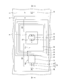
図2は、図1に示した回路部200の平面図である。図2のA-A方向から見た断面図が、図1に相当する。図2に示すように、pウェル8は、例えばnウェル9の周囲を囲むように枠状(環状)に設けられている。エッジ構造201は、例えばnウェル9の左側に配置されている。エッジ構造201は、nウェル9の外周部に複数個配置されていてもよい。なお、pウェル8、nウェル9及びエッジ構造201の平面レイアウトは特に限定されない。
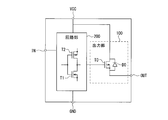
図3は、図1に示した実施形態に係る半導体集積回路の等価回路図を示す。図3からも、実施形態に係る半導体集積回路は、出力部100及び回路部200を備えることが理解できる。回路部200の第1回路素子T1及び第2回路素子T2は、例えば出力部100を制御する制御回路の一部に相当する。図3では図示を省略するが、第2回路素子T2のドレイン側には図1に示したスイッチング素子T3が接続されている。図3に示すように、出力部100の出力段素子T0には還流ダイオードD0が接続されている。出力段素子T0の第1主電極領域(ドレイン領域)が第1電位端子VCCに接続され、第2主電極領域(ソース領域)が出力端子OUTに接続されている。
図4は、図1に示した実施形態に係る半導体集積回路のエッジ構造201の等価回路を示す。E型トランジスタT11の第1主端子領域(ソース領域)はnウェル9と等電位の電位供給端子VNWに接続されている。E型トランジスタT11の第2主端子領域(ドレイン領域)は第1電位端子VCCに接続されている。E型トランジスタT11の閾値電圧Vthは例えば1V程度である。
図4に示すように、ツェナーダイオードD1の第3主端子領域(アノード領域)は、第2電位端子GNDに接続されている。ツェナーダイオードD1の第4主端子領域(カソード領域)は、E型トランジスタT11の第1制御電極(ゲート電極)、D型トランジスタT12の第2制御電極(ゲート電極)及び第5主端子領域(ソース領域)に接続されている。ツェナーダイオードD1の降伏電圧Vzは、例えば5V~10V程度である。ツェナーダイオードD1は定電圧Vzを出力する。
D型トランジスタT12の第6主端子領域(ドレイン領域)は、第1電位端子VCC及びE型トランジスタT11の第2主端子領域(ドレイン領域)に接続されている。D型トランジスタT12は、ピンチ抵抗として機能する。
E型トランジスタT11のソースの第3電位V3は、以下の式で表される。
V3=V2+Vz-Vth-α …(1)
式(1)において、αはバックゲート効果であり、例えば1V~2V程度である。適切な特性のトランジスタ、ツェナーダイオードを選択することにより、第3電位V3は、第2電位端子GNDの第2電位V2よりも高く設定することが可能である。第3電位V3は、例えば5V~10V程度である。nウェル9の電位は、E型トランジスタT11のソースの第3電位V3によりクランプされる。
<比較例>
ここで、図5を参照して、比較例に係る半導体集積回路を説明する。図5では、図1に示した出力部100の図示を省略している。比較例に係る半導体集積回路では、図5に示すように、図1に示したエッジ構造201が無い点が、図1に示した半導体集積回路と異なる。nウェル9には、電位供給端子VNWが接続されている。電位供給端子VNWには、回路部200とは異なる領域に設けられた回路(図示省略)が接続されている。
ここで、図5を参照して、比較例に係る半導体集積回路を説明する。図5では、図1に示した出力部100の図示を省略している。比較例に係る半導体集積回路では、図5に示すように、図1に示したエッジ構造201が無い点が、図1に示した半導体集積回路と異なる。nウェル9には、電位供給端子VNWが接続されている。電位供給端子VNWには、回路部200とは異なる領域に設けられた回路(図示省略)が接続されている。
比較例に係る半導体集積回路の通常動作時は、第1電位端子VCCには第1電位V1が印加される。また、第2電位端子GNDには、第1電位V1よりも低い第2電位V2が印加される。また、電位供給端子VNWには、第1電位V1よりも低く、且つ第2電位V2よりも高い第3電位V3が、回路部200とは異なる領域に設けられた回路から印加される。即ち、V1>V3>V2の電位関係で回路を動作させる。
一方、比較例に係る半導体集積回路の通常動作時以外である待機時等の特定時には、第1電位端子VCCには、通常動作時と同様の第1電位V1が印加されるが、低消費電力化のため、第3電位V3を第2電位V2と同等まで低下させ、nウェル9全体が例えば接地電位となるように制御する(V2=V3=GND)。本発明者らは、この制御状態で高温になるとリーク電流が増大し、n-型の高比抵抗層2、pウェル8及びnウェル9で構成されるn-p-n接合構造のパンチスルー耐圧が低下するという知見を得た。なお、図5の矢印はパンチスルーを模式的に示している。
そこで、実施形態に係る半導体集積回路では、図1,図2及び図4に示すように、nウェル9の外周部のpウェル8内にエッジ構造201を設けている。エッジ構造201が、常にnウェル9の第3電位V3をpウェル8の第2電位V2よりも高く制御することにより、待機時等の特定時においても第3電位V3が第2電位V2よりも高くなる。このため、図5に示した比較例に係る半導体集積回路のような高温時のリーク電流を低減することができ、n-型の高比抵抗層2、pウェル8及びnウェル9で構成されるn-p-n接合構造におけるパンチスルー耐圧の低下を防止することができる。更に、回路部200のpウェル8内でエッジ構造201が一体化しているため、pウェル8の外部に個別の回路を付加する必要が無く、小面積で実現可能となる。
更に、E型トランジスタT11の第1主端子領域(ソース領域)を、nウェル9との共通領域とし、D型トランジスタT12の第5主端子領域(ソース領域)を、第4主端子領域24との共有領域とし、D型トランジスタT12の第6主端子領域(ドレイン領域)を、第2主端子領域19との共有領域とすることにより、小面積化を図ることができる。
なお、図1では、E型トランジスタT11の第1主端子領域(ソース領域)を、nウェル9との共通領域とする場合を例示したが、E型トランジスタT11の第1主端子領域(ソース領域)を、nウェル9とは個別に設けてもよい。また、D型トランジスタT12の第5主端子領域(ソース領域)を、ツェナーダイオードD1の第4主端子領域24との共有領域とする場合を例示したが、D型トランジスタT12の第5主端子領域(ソース領域)を、ツェナーダイオードD1の第4主端子領域24とは個別に設けてもよい。また、D型トランジスタT12の第6主端子領域(ドレイン領域)を、E型トランジスタT11の第2主端子領域19との共有領域とする場合を例示したが、D型トランジスタT12の第6主端子領域(ドレイン領域)を、E型トランジスタT11の第2主端子領域19とは個別に設けてもよい。
更に、図1に示したE型トランジスタT11のゲート長L1が、D型トランジスタT12のゲート長L2よりも短く、且つ図2に示したE型トランジスタT11のゲート幅W1が、D型トランジスタT12のゲート幅W2よりも大きい。これにより、D型トランジスタT12の電流を絞り込み、消費電流を低減することができると共に、E型トランジスタT11では大電流を流し易くすることができる。ゲート長L1とゲート長L2とを同じ長さとしてもよいし、ゲート長L1をゲート長L2よりも長くしてもよい。また、ゲート幅W1とゲート幅W2とを同じ幅としてもよいし、ゲート幅W1をゲート幅W2より小さくしてもよい。
<実施例>
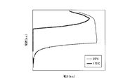
図6は、比較例に係る半導体集積回路の25℃及び175℃のI-V特性のシミュレーション結果を示し、図7は、実施形態に係る半導体集積回路の25℃及び175℃のI-V特性のシミュレーション結果を示す。図6に示す比較例に係る半導体集積回路では、第2電位V2及び第3電位V3として0Vを印加した状態で、第1電位V1を変化させた。一方、図7に示す実施形態に係る半導体集積回路では、第2電位V2として0Vを印加し、第3電位V3として第2電位V2よりも大きい5Vを印加した状態で、第1電位V1を変化させた。図6に示す比較例に係る半導体集積回路では、175℃でリーク電流が増大し、パンチスルー耐圧が低下している。これに対して、図7に示す実施形態に係る半導体集積回路では、175℃でのリーク電流が抑制され、パンチスルー耐圧が改善していることが分かる。
図6は、比較例に係る半導体集積回路の25℃及び175℃のI-V特性のシミュレーション結果を示し、図7は、実施形態に係る半導体集積回路の25℃及び175℃のI-V特性のシミュレーション結果を示す。図6に示す比較例に係る半導体集積回路では、第2電位V2及び第3電位V3として0Vを印加した状態で、第1電位V1を変化させた。一方、図7に示す実施形態に係る半導体集積回路では、第2電位V2として0Vを印加し、第3電位V3として第2電位V2よりも大きい5Vを印加した状態で、第1電位V1を変化させた。図6に示す比較例に係る半導体集積回路では、175℃でリーク電流が増大し、パンチスルー耐圧が低下している。これに対して、図7に示す実施形態に係る半導体集積回路では、175℃でのリーク電流が抑制され、パンチスルー耐圧が改善していることが分かる。
<変形例>
実施形態の変形例に係る半導体集積回路は、図8及び図9に示すように、E型トランジスタT11の平面パターンが、pウェル8の周囲を取り囲むように枠状(環状)に設けられている点が、図1及び図2に示した実施形態に係る半導体集積回路と異なる。図8は、図9の平面図に示したA-A方向から見た断面図に相当する。E型トランジスタT11の平面パターンを枠状とすることにより、E型トランジスタT11のゲート幅を大きくすることができ、E型トランジスタT11に大電流を流れ易くすることができる。図8及び図9では、図1及び図2に示した第1回路素子T1は図示を省略しているが、例えばE型トランジスタT11の周囲を取り囲むpウェル8内に設けられる。
実施形態の変形例に係る半導体集積回路は、図8及び図9に示すように、E型トランジスタT11の平面パターンが、pウェル8の周囲を取り囲むように枠状(環状)に設けられている点が、図1及び図2に示した実施形態に係る半導体集積回路と異なる。図8は、図9の平面図に示したA-A方向から見た断面図に相当する。E型トランジスタT11の平面パターンを枠状とすることにより、E型トランジスタT11のゲート幅を大きくすることができ、E型トランジスタT11に大電流を流れ易くすることができる。図8及び図9では、図1及び図2に示した第1回路素子T1は図示を省略しているが、例えばE型トランジスタT11の周囲を取り囲むpウェル8内に設けられる。
(その他の実施形態)
上記のように、本発明は実施形態によって記載したが、この開示の一部をなす論述及び図面は本発明を限定するものであると理解すべきではない。この開示から当業者には様々な代替実施の形態、実施例及び運用技術が明らかとなろう。
上記のように、本発明は実施形態によって記載したが、この開示の一部をなす論述及び図面は本発明を限定するものであると理解すべきではない。この開示から当業者には様々な代替実施の形態、実施例及び運用技術が明らかとなろう。
例えば、実施形態では、出力部100の出力段素子T0としてトレンチゲート型のMOSトランジスタを例示したが、これに限定されない。例えば、出力段素子T0がトレンチゲート型のIGBTであってもよい。出力段素子T0がIGBTの場合は、例えば、図1の低比抵抗層1をp+型の半導体層とすればよい。また、回路部200に含まれる制御用の回路として、第1回路素子T1及び第2回路素子T2から構成されるCMOSを例示したが、CMOSに限定されず、他の半導体素子からなる制御用の回路であっても構わない。
また、実施形態では、半導体基体(1,2)としてSiを用いた場合を例示した。しかし、Siの他にも、炭化ケイ素(SiC)、窒化ガリウム(GaN)、ダイヤモンド又は窒化アルミニウム(AlN)等のSiよりも禁制帯幅が広い半導体(ワイドバンドギャップ半導体)材料を用いた場合にも適用可能である。
また、図1では、半導体基体(1,2)がn+型の半導体基板からなる低比抵抗層1上に、n-型の高比抵抗層2がエピタキシャル成長された構造を例示したが、これに限定されない。例えば、低比抵抗層1の代わりに、p型の支持基板(半導体ウェハ)の上にエピタキシャル成長されたn+型の埋め込み層を用い、このn+型の埋め込み層の上にn-型の高比抵抗層2をエピタキシャル成長して3層構造の半導体基体を構成してもよい。低比抵抗層1の代わりにn+型の埋め込みエピタキシャル層を用いた3層構造の半導体基体の場合は、高比抵抗層2の上面から埋め込みエピタキシャル層に届くシンカー領域を設ければよい。即ち、シンカー領域を介してドレイン領域として機能するn+型の埋め込みエピタキシャル層に高比抵抗層2の上面側から接続してもよい。この場合、ドレイン電極配線は高比抵抗層2の上面側に設けられる。低比抵抗層1の代わりにn+型の埋め込みエピタキシャル層を用いる場合は、下面側の支持基板を絶縁体基板としてSOI構造にしても構わない。
このように、本発明はここでは記載していない様々な実施の形態等を含むことは勿論である。したがって、本発明の技術的範囲は上記の説明から妥当な特許請求の範囲に係る発明特定事項によってのみ定められるものである。
1…低比抵抗層
2…高比抵抗層(第1主電極領域)
3…ボディ領域
4a,4b…第2主電極領域
5…ベースコンタクト領域
6a,6b,17,21,26…ゲート絶縁膜
7a,7b,13,18,22,27…ゲート電極
8…第1ウェル
9…第2ウェル(第1主端子領域)
10…第3主電極領域
11…第4主電極領域
14…基体コンタクト領域
15…第5主電極領域
16…第6主電極領域
19…第2主端子領域(第6主端子領域)
20…エッジコンタクト領域
23…第3主端子領域
24…第4主端子領域(第5主端子領域)
25…チャネル形成領域
28…ウェルコンタクト領域
29…下面電極
30a,30b…ゲートトレンチ
31,31…配線
33…インバータ
100…出力部
200…回路部
201…エッジ構造
D0…還流ダイオード
D1…ツェナーダイオード
T0…出力段素子
T1…第1回路素子
T2…第2回路素子
T3…スイッチング素子
T11…エンハンスメント型トランジスタ
T12…デプレッション型トランジスタ
2…高比抵抗層(第1主電極領域)
3…ボディ領域
4a,4b…第2主電極領域
5…ベースコンタクト領域
6a,6b,17,21,26…ゲート絶縁膜
7a,7b,13,18,22,27…ゲート電極
8…第1ウェル
9…第2ウェル(第1主端子領域)
10…第3主電極領域
11…第4主電極領域
14…基体コンタクト領域
15…第5主電極領域
16…第6主電極領域
19…第2主端子領域(第6主端子領域)
20…エッジコンタクト領域
23…第3主端子領域
24…第4主端子領域(第5主端子領域)
25…チャネル形成領域
28…ウェルコンタクト領域
29…下面電極
30a,30b…ゲートトレンチ
31,31…配線
33…インバータ
100…出力部
200…回路部
201…エッジ構造
D0…還流ダイオード
D1…ツェナーダイオード
T0…出力段素子
T1…第1回路素子
T2…第2回路素子
T3…スイッチング素子
T11…エンハンスメント型トランジスタ
T12…デプレッション型トランジスタ
Claims (14)
- 第1導電型の半導体基体と、
前記半導体基体の下面に設けられ、第1電位が印加される下面電極と、
前記半導体基体の上面側に設けられ、前記第1電位よりも低い第2電位が印加される第2導電型の第1ウェルと、
前記第1ウェル内に設けられた第1導電型の第2ウェルと、
前記第1ウェルに設けられ、前記第2電位よりも高い第3電位を前記第2ウェルに供給するエッジ構造と、
を備えることを特徴とする半導体集積回路。 - 前記エッジ構造は、
前記第2ウェルと電位が等しく前記第3電位を供給する第1導電型の第1主端子領域、前記第1電位が印加される第1導電型の第2主端子領域、及び前記第1主端子領域と前記第2主端子領域の間を流れる電流を制御する第1制御電極を有するエンハンスメント型トランジスタと、
前記第2電位が印加される第2導電型の第3主端子領域、及び前記第1制御電極に接続された第1導電型の第4主端子領域を有するツェナーダイオードと、
前記第4主端子領域に接続された第1導電型の第5主端子領域、前記第1電位が印加される第1導電型の第6主端子領域、及び前記第1制御電極に接続され前記第5主端子領域と前記第6主端子領域の間を流れる電流を制御する第2制御電極を有するデプレッション型トランジスタと、
を備えることを特徴とする請求項1に記載の半導体集積回路。 - 前記第1主端子領域が、前記第2ウェルとの共有領域で構成されることを特徴とする請求項2に記載の半導体集積回路。
- 前記第2主端子領域が、前記第1ウェル内に前記第1主端子領域から離間して設けられ、前記半導体基体と第1配線を介して接続されていることを特徴とする請求項2又は3に記載の半導体集積回路。
- 前記エンハンスメント型トランジスタが、前記第1主端子領域と前記第2主端子領域との間の前記第1ウェル上に設けられた第1ゲート絶縁膜を更に備え、
前記第1制御電極が、前記第1ゲート絶縁膜上に設けられていることを特徴とする請求項2~4のいずれか1項に記載の半導体集積回路。 - 前記第3主端子領域が、前記第1ウェル内に前記第2ウェル及び前記第2主端子領域から離間して設けられ、前記第1ウェルよりも高不純物濃度の半導体領域であることを特徴とする請求項2~5のいずれか1項に記載の半導体集積回路。
- 前記第4主端子領域が、前記第3主端子領域内に設けられ、前記第3主端子領域とpn接合をなすことを特徴とする請求項2~6に記載の半導体集積回路。
- 前記第5主端子領域が、前記第4主端子領域との共有領域で構成されることを特徴とする請求項請求項2~7のいずれか1項に記載の半導体集積回路。
- 前記第6主端子領域が、前記第2主端子領域との共有領域で構成されることを特徴とする請求項請求項2~8のいずれか1項に記載の半導体集積回路。
- 前記デプレッション型トランジスタが、
前記第5主端子領域と前記第6主端子領域の間に設けられ、前記第3主端子領域と重複する部分の導電型が反転可能な第1導電型のチャネル形成領域と、
前記チャネル形成領域上に設けられた第2ゲート絶縁膜と、
を更に備え、
前記第2制御電極が前記第2ゲート絶縁膜上に設けられ、前記第5主端子領域及び前記第1制御電極と第2配線を介して接続されている
ことを特徴とする請求項2~9のいずれか1項に記載の半導体集積回路。 - 前記ツェナーダイオードは、5V~10Vの降伏電圧を有することを特徴とする請求項2~10のいずれか1項に記載の半導体集積回路。
- 前記エンハンスメント型トランジスタのゲート長が、前記デプレッション型トランジスタのゲート長よりも短いことを特徴とする請求項2~11のいずれか1項に記載の半導体集積回路。
- 前記エンハンスメント型トランジスタのゲート幅が、前記デプレッション型トランジスタのゲート幅よりも広いことを特徴とする請求項2~12のいずれか1項に記載の半導体集積回路。
- 前記エンハンスメント型トランジスタの平面パターンが、前記第2ウェルを取り囲むように設けられていることを特徴とする請求項2~13のいずれか1項に記載の半導体集積回路。
Priority Applications (3)
| Application Number | Priority Date | Filing Date | Title |
|---|---|---|---|
| CN202080005944.1A CN112956025B (zh) | 2019-05-16 | 2020-03-27 | 半导体集成电路 |
| JP2021519298A JP7115637B2 (ja) | 2019-05-16 | 2020-03-27 | 半導体集積回路 |
| US17/238,908 US11948937B2 (en) | 2019-05-16 | 2021-04-23 | Semiconductor integrated circuit with edge structure to decrease leakage current |
Applications Claiming Priority (2)
| Application Number | Priority Date | Filing Date | Title |
|---|---|---|---|
| JP2019093138 | 2019-05-16 | ||
| JP2019-093138 | 2019-05-16 |
Related Child Applications (1)
| Application Number | Title | Priority Date | Filing Date |
|---|---|---|---|
| US17/238,908 Continuation US11948937B2 (en) | 2019-05-16 | 2021-04-23 | Semiconductor integrated circuit with edge structure to decrease leakage current |
Publications (1)
| Publication Number | Publication Date |
|---|---|
| WO2020230465A1 true WO2020230465A1 (ja) | 2020-11-19 |
Family
ID=73289024
Family Applications (1)
| Application Number | Title | Priority Date | Filing Date |
|---|---|---|---|
| PCT/JP2020/014219 Ceased WO2020230465A1 (ja) | 2019-05-16 | 2020-03-27 | 半導体集積回路 |
Country Status (4)
| Country | Link |
|---|---|
| US (1) | US11948937B2 (ja) |
| JP (1) | JP7115637B2 (ja) |
| CN (1) | CN112956025B (ja) |
| WO (1) | WO2020230465A1 (ja) |
Cited By (1)
| Publication number | Priority date | Publication date | Assignee | Title |
|---|---|---|---|---|
| KR20220150109A (ko) * | 2021-05-03 | 2022-11-10 | 에스케이하이닉스 주식회사 | 반도체 장치 및 그 제조방법 |
Families Citing this family (2)
| Publication number | Priority date | Publication date | Assignee | Title |
|---|---|---|---|---|
| US11398565B2 (en) * | 2020-12-07 | 2022-07-26 | Globalfoundries Singapore Pte. Ltd. | Silicon controlled rectifier with a gate electrode for electrostatic discharge protection |
| JP7722031B2 (ja) * | 2021-08-12 | 2025-08-13 | 富士電機株式会社 | 半導体装置 |
Citations (4)
| Publication number | Priority date | Publication date | Assignee | Title |
|---|---|---|---|---|
| JP2005191263A (ja) * | 2003-12-25 | 2005-07-14 | Fuji Electric Device Technology Co Ltd | 半導体装置 |
| JP2016042558A (ja) * | 2014-08-19 | 2016-03-31 | 富士電機株式会社 | 半導体装置 |
| WO2016132418A1 (ja) * | 2015-02-18 | 2016-08-25 | 富士電機株式会社 | 半導体集積回路 |
| WO2016132417A1 (ja) * | 2015-02-18 | 2016-08-25 | 富士電機株式会社 | 半導体集積回路 |
Family Cites Families (10)
| Publication number | Priority date | Publication date | Assignee | Title |
|---|---|---|---|---|
| JPH07211802A (ja) * | 1994-01-19 | 1995-08-11 | Fujitsu Ltd | 半導体集積回路 |
| JP3413569B2 (ja) * | 1998-09-16 | 2003-06-03 | 株式会社日立製作所 | 絶縁ゲート型半導体装置およびその製造方法 |
| JP2003258118A (ja) * | 2002-03-06 | 2003-09-12 | Seiko Epson Corp | 半導体装置 |
| WO2006003729A1 (ja) | 2004-07-02 | 2006-01-12 | Matsushita Electric Industrial Co., Ltd. | 半導体集積回路 |
| JP4530823B2 (ja) * | 2004-12-02 | 2010-08-25 | 三洋電機株式会社 | 半導体装置及びその製造方法 |
| WO2008012899A1 (fr) | 2006-07-27 | 2008-01-31 | Fujitsu Limited | Dispositif de circuit à semi-conducteurs, système de dispositif de circuit à semi-conducteurs et procédé de fabrication pour le dispositif de circuit à semi-conducteurs |
| WO2008036047A1 (en) | 2006-09-21 | 2008-03-27 | Nanyang Technological University | Triple well transmit-receive switch transistor |
| JP6610114B2 (ja) * | 2015-09-16 | 2019-11-27 | 富士電機株式会社 | 半導体装置および半導体装置の製造方法 |
| JP6845688B2 (ja) | 2016-12-28 | 2021-03-24 | ラピスセミコンダクタ株式会社 | スイッチデバイス及びスイッチ回路 |
| CN110828564B (zh) * | 2018-08-13 | 2022-04-08 | 香港科技大学 | 具有半导体性栅极的场效应晶体管 |
-
2020
- 2020-03-27 CN CN202080005944.1A patent/CN112956025B/zh active Active
- 2020-03-27 JP JP2021519298A patent/JP7115637B2/ja active Active
- 2020-03-27 WO PCT/JP2020/014219 patent/WO2020230465A1/ja not_active Ceased
-
2021
- 2021-04-23 US US17/238,908 patent/US11948937B2/en active Active
Patent Citations (4)
| Publication number | Priority date | Publication date | Assignee | Title |
|---|---|---|---|---|
| JP2005191263A (ja) * | 2003-12-25 | 2005-07-14 | Fuji Electric Device Technology Co Ltd | 半導体装置 |
| JP2016042558A (ja) * | 2014-08-19 | 2016-03-31 | 富士電機株式会社 | 半導体装置 |
| WO2016132418A1 (ja) * | 2015-02-18 | 2016-08-25 | 富士電機株式会社 | 半導体集積回路 |
| WO2016132417A1 (ja) * | 2015-02-18 | 2016-08-25 | 富士電機株式会社 | 半導体集積回路 |
Cited By (2)
| Publication number | Priority date | Publication date | Assignee | Title |
|---|---|---|---|---|
| KR20220150109A (ko) * | 2021-05-03 | 2022-11-10 | 에스케이하이닉스 주식회사 | 반도체 장치 및 그 제조방법 |
| KR102911242B1 (ko) * | 2021-05-03 | 2026-01-13 | 에스케이하이닉스 주식회사 | 반도체 장치 및 그 제조방법 |
Also Published As
| Publication number | Publication date |
|---|---|
| JP7115637B2 (ja) | 2022-08-09 |
| CN112956025B (zh) | 2024-06-28 |
| US11948937B2 (en) | 2024-04-02 |
| CN112956025A (zh) | 2021-06-11 |
| US20210242198A1 (en) | 2021-08-05 |
| JPWO2020230465A1 (ja) | 2021-10-28 |
Similar Documents
| Publication | Publication Date | Title |
|---|---|---|
| US6503782B2 (en) | Complementary accumulation-mode JFET integrated circuit topology using wide (>2eV) bandgap semiconductors | |
| US11502164B2 (en) | Method of manufacturing semiconductor integrated circuit | |
| JP6579273B2 (ja) | 半導体集積回路 | |
| JP7472522B2 (ja) | 半導体集積回路 | |
| JP7115637B2 (ja) | 半導体集積回路 | |
| JP2007134588A (ja) | 半導体装置 | |
| EP2924723B1 (en) | Integrated circuit | |
| US5889310A (en) | Semiconductor device with high breakdown voltage island region | |
| CN106486480A (zh) | 半导体器件 | |
| US7199403B2 (en) | Semiconductor arrangement having a MOSFET structure and a zener device | |
| JP2013247188A (ja) | 半導体装置 | |
| JP2019145537A (ja) | 半導体集積回路の製造方法 | |
| US6010950A (en) | Method of manufacturing semiconductor bonded substrate | |
| US20240421197A1 (en) | Semiconductor device | |
| JP2013041891A (ja) | 半導体装置 | |
| CN100477261C (zh) | 半导体器件 | |
| CN115939122A (zh) | 半导体装置 | |
| JP2022095150A (ja) | 半導体装置 | |
| JP7771708B2 (ja) | 半導体装置 | |
| JP2024059155A (ja) | 半導体装置 | |
| JP2629434B2 (ja) | アノードショート伝導度変調型misfetを備えた半導体装置 | |
| JP2024108876A (ja) | 半導体装置 | |
| JP2025030648A (ja) | 半導体素子、複合半導体素子、駆動回路 | |
| CN121645981A (zh) | 半导体装置 | |
| JPH06291322A (ja) | 縦型電界効果トランジスタ |
Legal Events
| Date | Code | Title | Description |
|---|---|---|---|
| 121 | Ep: the epo has been informed by wipo that ep was designated in this application |
Ref document number: 20805821 Country of ref document: EP Kind code of ref document: A1 |
|
| ENP | Entry into the national phase |
Ref document number: 2021519298 Country of ref document: JP Kind code of ref document: A |
|
| NENP | Non-entry into the national phase |
Ref country code: DE |
|
| 122 | Ep: pct application non-entry in european phase |
Ref document number: 20805821 Country of ref document: EP Kind code of ref document: A1 |