EP2924723B1 - Integrated circuit - Google Patents
Integrated circuit Download PDFInfo
- Publication number
- EP2924723B1 EP2924723B1 EP15154323.8A EP15154323A EP2924723B1 EP 2924723 B1 EP2924723 B1 EP 2924723B1 EP 15154323 A EP15154323 A EP 15154323A EP 2924723 B1 EP2924723 B1 EP 2924723B1
- Authority
- EP
- European Patent Office
- Prior art keywords
- region
- diffusion region
- type diffusion
- semiconductor region
- type
- Prior art date
- Legal status (The legal status is an assumption and is not a legal conclusion. Google has not performed a legal analysis and makes no representation as to the accuracy of the status listed.)
- Active
Links
- 239000004065 semiconductor Substances 0.000 claims description 217
- 239000012535 impurity Substances 0.000 claims description 114
- 239000000758 substrate Substances 0.000 claims description 97
- 239000002344 surface layer Substances 0.000 claims description 35
- 238000002955 isolation Methods 0.000 claims description 25
- 230000005669 field effect Effects 0.000 claims description 16
- 238000009830 intercalation Methods 0.000 claims description 5
- 238000009792 diffusion process Methods 0.000 description 568
- 238000010276 construction Methods 0.000 description 62
- 230000015556 catabolic process Effects 0.000 description 56
- 239000010410 layer Substances 0.000 description 49
- 230000005856 abnormality Effects 0.000 description 17
- 230000002093 peripheral effect Effects 0.000 description 14
- 239000011229 interlayer Substances 0.000 description 13
- 230000005684 electric field Effects 0.000 description 9
- 230000000149 penetrating effect Effects 0.000 description 9
- 239000000463 material Substances 0.000 description 8
- 230000008054 signal transmission Effects 0.000 description 8
- 238000000034 method Methods 0.000 description 7
- VYPSYNLAJGMNEJ-UHFFFAOYSA-N Silicium dioxide Chemical compound O=[Si]=O VYPSYNLAJGMNEJ-UHFFFAOYSA-N 0.000 description 4
- XUIMIQQOPSSXEZ-UHFFFAOYSA-N Silicon Chemical compound [Si] XUIMIQQOPSSXEZ-UHFFFAOYSA-N 0.000 description 4
- 238000010586 diagram Methods 0.000 description 4
- 230000000694 effects Effects 0.000 description 4
- 229910052710 silicon Inorganic materials 0.000 description 4
- 239000010703 silicon Substances 0.000 description 4
- NAWXUBYGYWOOIX-SFHVURJKSA-N (2s)-2-[[4-[2-(2,4-diaminoquinazolin-6-yl)ethyl]benzoyl]amino]-4-methylidenepentanedioic acid Chemical compound C1=CC2=NC(N)=NC(N)=C2C=C1CCC1=CC=C(C(=O)N[C@@H](CC(=C)C(O)=O)C(O)=O)C=C1 NAWXUBYGYWOOIX-SFHVURJKSA-N 0.000 description 3
- 230000002159 abnormal effect Effects 0.000 description 3
- 230000003321 amplification Effects 0.000 description 3
- 238000004364 calculation method Methods 0.000 description 3
- 238000006073 displacement reaction Methods 0.000 description 3
- 238000007667 floating Methods 0.000 description 3
- 238000009413 insulation Methods 0.000 description 3
- 238000003199 nucleic acid amplification method Methods 0.000 description 3
- 238000005457 optimization Methods 0.000 description 3
- 230000003647 oxidation Effects 0.000 description 3
- 238000007254 oxidation reaction Methods 0.000 description 3
- 230000008569 process Effects 0.000 description 3
- 239000003990 capacitor Substances 0.000 description 2
- 238000006243 chemical reaction Methods 0.000 description 2
- 229910052681 coesite Inorganic materials 0.000 description 2
- 229910052906 cristobalite Inorganic materials 0.000 description 2
- 230000007423 decrease Effects 0.000 description 2
- 230000003247 decreasing effect Effects 0.000 description 2
- 238000001514 detection method Methods 0.000 description 2
- 238000005516 engineering process Methods 0.000 description 2
- 238000005468 ion implantation Methods 0.000 description 2
- 230000007257 malfunction Effects 0.000 description 2
- 229910044991 metal oxide Inorganic materials 0.000 description 2
- 150000004706 metal oxides Chemical class 0.000 description 2
- 230000004048 modification Effects 0.000 description 2
- 238000012986 modification Methods 0.000 description 2
- 230000003071 parasitic effect Effects 0.000 description 2
- 229910021420 polycrystalline silicon Inorganic materials 0.000 description 2
- 239000000377 silicon dioxide Substances 0.000 description 2
- 229910052682 stishovite Inorganic materials 0.000 description 2
- 229910052905 tridymite Inorganic materials 0.000 description 2
- 239000000370 acceptor Substances 0.000 description 1
- 230000002411 adverse Effects 0.000 description 1
- 230000000903 blocking effect Effects 0.000 description 1
- 239000000969 carrier Substances 0.000 description 1
- 230000008859 change Effects 0.000 description 1
- 230000007812 deficiency Effects 0.000 description 1
- 238000006731 degradation reaction Methods 0.000 description 1
- 230000001419 dependent effect Effects 0.000 description 1
- 230000000779 depleting effect Effects 0.000 description 1
- 238000007599 discharging Methods 0.000 description 1
- 238000010292 electrical insulation Methods 0.000 description 1
- 238000013021 overheating Methods 0.000 description 1
- 230000009467 reduction Effects 0.000 description 1
- 239000013643 reference control Substances 0.000 description 1
Images


Classifications
-
- H—ELECTRICITY
- H01—ELECTRIC ELEMENTS
- H01L—SEMICONDUCTOR DEVICES NOT COVERED BY CLASS H10
- H01L27/00—Devices consisting of a plurality of semiconductor or other solid-state components formed in or on a common substrate
- H01L27/02—Devices consisting of a plurality of semiconductor or other solid-state components formed in or on a common substrate including semiconductor components specially adapted for rectifying, oscillating, amplifying or switching and having potential barriers; including integrated passive circuit elements having potential barriers
- H01L27/04—Devices consisting of a plurality of semiconductor or other solid-state components formed in or on a common substrate including semiconductor components specially adapted for rectifying, oscillating, amplifying or switching and having potential barriers; including integrated passive circuit elements having potential barriers the substrate being a semiconductor body
- H01L27/06—Devices consisting of a plurality of semiconductor or other solid-state components formed in or on a common substrate including semiconductor components specially adapted for rectifying, oscillating, amplifying or switching and having potential barriers; including integrated passive circuit elements having potential barriers the substrate being a semiconductor body including a plurality of individual components in a non-repetitive configuration
- H01L27/0611—Devices consisting of a plurality of semiconductor or other solid-state components formed in or on a common substrate including semiconductor components specially adapted for rectifying, oscillating, amplifying or switching and having potential barriers; including integrated passive circuit elements having potential barriers the substrate being a semiconductor body including a plurality of individual components in a non-repetitive configuration integrated circuits having a two-dimensional layout of components without a common active region
- H01L27/0617—Devices consisting of a plurality of semiconductor or other solid-state components formed in or on a common substrate including semiconductor components specially adapted for rectifying, oscillating, amplifying or switching and having potential barriers; including integrated passive circuit elements having potential barriers the substrate being a semiconductor body including a plurality of individual components in a non-repetitive configuration integrated circuits having a two-dimensional layout of components without a common active region comprising components of the field-effect type
- H01L27/0635—Devices consisting of a plurality of semiconductor or other solid-state components formed in or on a common substrate including semiconductor components specially adapted for rectifying, oscillating, amplifying or switching and having potential barriers; including integrated passive circuit elements having potential barriers the substrate being a semiconductor body including a plurality of individual components in a non-repetitive configuration integrated circuits having a two-dimensional layout of components without a common active region comprising components of the field-effect type in combination with bipolar transistors and diodes, or resistors, or capacitors
-
- H—ELECTRICITY
- H01—ELECTRIC ELEMENTS
- H01L—SEMICONDUCTOR DEVICES NOT COVERED BY CLASS H10
- H01L21/00—Processes or apparatus adapted for the manufacture or treatment of semiconductor or solid state devices or of parts thereof
- H01L21/70—Manufacture or treatment of devices consisting of a plurality of solid state components formed in or on a common substrate or of parts thereof; Manufacture of integrated circuit devices or of parts thereof
- H01L21/71—Manufacture of specific parts of devices defined in group H01L21/70
- H01L21/76—Making of isolation regions between components
- H01L21/761—PN junctions
-
- H—ELECTRICITY
- H01—ELECTRIC ELEMENTS
- H01L—SEMICONDUCTOR DEVICES NOT COVERED BY CLASS H10
- H01L21/00—Processes or apparatus adapted for the manufacture or treatment of semiconductor or solid state devices or of parts thereof
- H01L21/70—Manufacture or treatment of devices consisting of a plurality of solid state components formed in or on a common substrate or of parts thereof; Manufacture of integrated circuit devices or of parts thereof
- H01L21/77—Manufacture or treatment of devices consisting of a plurality of solid state components or integrated circuits formed in, or on, a common substrate
- H01L21/78—Manufacture or treatment of devices consisting of a plurality of solid state components or integrated circuits formed in, or on, a common substrate with subsequent division of the substrate into plural individual devices
- H01L21/82—Manufacture or treatment of devices consisting of a plurality of solid state components or integrated circuits formed in, or on, a common substrate with subsequent division of the substrate into plural individual devices to produce devices, e.g. integrated circuits, each consisting of a plurality of components
- H01L21/822—Manufacture or treatment of devices consisting of a plurality of solid state components or integrated circuits formed in, or on, a common substrate with subsequent division of the substrate into plural individual devices to produce devices, e.g. integrated circuits, each consisting of a plurality of components the substrate being a semiconductor, using silicon technology
- H01L21/8232—Field-effect technology
- H01L21/8234—MIS technology, i.e. integration processes of field effect transistors of the conductor-insulator-semiconductor type
- H01L21/8238—Complementary field-effect transistors, e.g. CMOS
- H01L21/823892—Complementary field-effect transistors, e.g. CMOS with a particular manufacturing method of the wells or tubs, e.g. twin tubs, high energy well implants, buried implanted layers for lateral isolation [BILLI]
-
- H—ELECTRICITY
- H01—ELECTRIC ELEMENTS
- H01L—SEMICONDUCTOR DEVICES NOT COVERED BY CLASS H10
- H01L27/00—Devices consisting of a plurality of semiconductor or other solid-state components formed in or on a common substrate
- H01L27/02—Devices consisting of a plurality of semiconductor or other solid-state components formed in or on a common substrate including semiconductor components specially adapted for rectifying, oscillating, amplifying or switching and having potential barriers; including integrated passive circuit elements having potential barriers
- H01L27/04—Devices consisting of a plurality of semiconductor or other solid-state components formed in or on a common substrate including semiconductor components specially adapted for rectifying, oscillating, amplifying or switching and having potential barriers; including integrated passive circuit elements having potential barriers the substrate being a semiconductor body
- H01L27/08—Devices consisting of a plurality of semiconductor or other solid-state components formed in or on a common substrate including semiconductor components specially adapted for rectifying, oscillating, amplifying or switching and having potential barriers; including integrated passive circuit elements having potential barriers the substrate being a semiconductor body including only semiconductor components of a single kind
- H01L27/085—Devices consisting of a plurality of semiconductor or other solid-state components formed in or on a common substrate including semiconductor components specially adapted for rectifying, oscillating, amplifying or switching and having potential barriers; including integrated passive circuit elements having potential barriers the substrate being a semiconductor body including only semiconductor components of a single kind including field-effect components only
- H01L27/088—Devices consisting of a plurality of semiconductor or other solid-state components formed in or on a common substrate including semiconductor components specially adapted for rectifying, oscillating, amplifying or switching and having potential barriers; including integrated passive circuit elements having potential barriers the substrate being a semiconductor body including only semiconductor components of a single kind including field-effect components only the components being field-effect transistors with insulated gate
- H01L27/092—Devices consisting of a plurality of semiconductor or other solid-state components formed in or on a common substrate including semiconductor components specially adapted for rectifying, oscillating, amplifying or switching and having potential barriers; including integrated passive circuit elements having potential barriers the substrate being a semiconductor body including only semiconductor components of a single kind including field-effect components only the components being field-effect transistors with insulated gate complementary MIS field-effect transistors
-
- H—ELECTRICITY
- H01—ELECTRIC ELEMENTS
- H01L—SEMICONDUCTOR DEVICES NOT COVERED BY CLASS H10
- H01L28/00—Passive two-terminal components without a potential-jump or surface barrier for integrated circuits; Details thereof; Multistep manufacturing processes therefor
- H01L28/20—Resistors
-
- H—ELECTRICITY
- H01—ELECTRIC ELEMENTS
- H01L—SEMICONDUCTOR DEVICES NOT COVERED BY CLASS H10
- H01L29/00—Semiconductor devices specially adapted for rectifying, amplifying, oscillating or switching and having potential barriers; Capacitors or resistors having potential barriers, e.g. a PN-junction depletion layer or carrier concentration layer; Details of semiconductor bodies or of electrodes thereof ; Multistep manufacturing processes therefor
- H01L29/02—Semiconductor bodies ; Multistep manufacturing processes therefor
- H01L29/06—Semiconductor bodies ; Multistep manufacturing processes therefor characterised by their shape; characterised by the shapes, relative sizes, or dispositions of the semiconductor regions ; characterised by the concentration or distribution of impurities within semiconductor regions
- H01L29/0603—Semiconductor bodies ; Multistep manufacturing processes therefor characterised by their shape; characterised by the shapes, relative sizes, or dispositions of the semiconductor regions ; characterised by the concentration or distribution of impurities within semiconductor regions characterised by particular constructional design considerations, e.g. for preventing surface leakage, for controlling electric field concentration or for internal isolations regions
- H01L29/0607—Semiconductor bodies ; Multistep manufacturing processes therefor characterised by their shape; characterised by the shapes, relative sizes, or dispositions of the semiconductor regions ; characterised by the concentration or distribution of impurities within semiconductor regions characterised by particular constructional design considerations, e.g. for preventing surface leakage, for controlling electric field concentration or for internal isolations regions for preventing surface leakage or controlling electric field concentration
- H01L29/0611—Semiconductor bodies ; Multistep manufacturing processes therefor characterised by their shape; characterised by the shapes, relative sizes, or dispositions of the semiconductor regions ; characterised by the concentration or distribution of impurities within semiconductor regions characterised by particular constructional design considerations, e.g. for preventing surface leakage, for controlling electric field concentration or for internal isolations regions for preventing surface leakage or controlling electric field concentration for increasing or controlling the breakdown voltage of reverse biased devices
- H01L29/0615—Semiconductor bodies ; Multistep manufacturing processes therefor characterised by their shape; characterised by the shapes, relative sizes, or dispositions of the semiconductor regions ; characterised by the concentration or distribution of impurities within semiconductor regions characterised by particular constructional design considerations, e.g. for preventing surface leakage, for controlling electric field concentration or for internal isolations regions for preventing surface leakage or controlling electric field concentration for increasing or controlling the breakdown voltage of reverse biased devices by the doping profile or the shape or the arrangement of the PN junction, or with supplementary regions, e.g. junction termination extension [JTE]
- H01L29/063—Reduced surface field [RESURF] pn-junction structures
- H01L29/0634—Multiple reduced surface field (multi-RESURF) structures, e.g. double RESURF, charge compensation, cool, superjunction (SJ), 3D-RESURF, composite buffer (CB) structures
-
- H—ELECTRICITY
- H01—ELECTRIC ELEMENTS
- H01L—SEMICONDUCTOR DEVICES NOT COVERED BY CLASS H10
- H01L29/00—Semiconductor devices specially adapted for rectifying, amplifying, oscillating or switching and having potential barriers; Capacitors or resistors having potential barriers, e.g. a PN-junction depletion layer or carrier concentration layer; Details of semiconductor bodies or of electrodes thereof ; Multistep manufacturing processes therefor
- H01L29/02—Semiconductor bodies ; Multistep manufacturing processes therefor
- H01L29/06—Semiconductor bodies ; Multistep manufacturing processes therefor characterised by their shape; characterised by the shapes, relative sizes, or dispositions of the semiconductor regions ; characterised by the concentration or distribution of impurities within semiconductor regions
- H01L29/10—Semiconductor bodies ; Multistep manufacturing processes therefor characterised by their shape; characterised by the shapes, relative sizes, or dispositions of the semiconductor regions ; characterised by the concentration or distribution of impurities within semiconductor regions with semiconductor regions connected to an electrode not carrying current to be rectified, amplified or switched and such electrode being part of a semiconductor device which comprises three or more electrodes
- H01L29/1095—Body region, i.e. base region, of DMOS transistors or IGBTs
-
- H—ELECTRICITY
- H01—ELECTRIC ELEMENTS
- H01L—SEMICONDUCTOR DEVICES NOT COVERED BY CLASS H10
- H01L29/00—Semiconductor devices specially adapted for rectifying, amplifying, oscillating or switching and having potential barriers; Capacitors or resistors having potential barriers, e.g. a PN-junction depletion layer or carrier concentration layer; Details of semiconductor bodies or of electrodes thereof ; Multistep manufacturing processes therefor
- H01L29/40—Electrodes ; Multistep manufacturing processes therefor
- H01L29/402—Field plates
- H01L29/405—Resistive arrangements, e.g. resistive or semi-insulating field plates
-
- H—ELECTRICITY
- H01—ELECTRIC ELEMENTS
- H01L—SEMICONDUCTOR DEVICES NOT COVERED BY CLASS H10
- H01L29/00—Semiconductor devices specially adapted for rectifying, amplifying, oscillating or switching and having potential barriers; Capacitors or resistors having potential barriers, e.g. a PN-junction depletion layer or carrier concentration layer; Details of semiconductor bodies or of electrodes thereof ; Multistep manufacturing processes therefor
- H01L29/66—Types of semiconductor device ; Multistep manufacturing processes therefor
- H01L29/68—Types of semiconductor device ; Multistep manufacturing processes therefor controllable by only the electric current supplied, or only the electric potential applied, to an electrode which does not carry the current to be rectified, amplified or switched
- H01L29/70—Bipolar devices
- H01L29/72—Transistor-type devices, i.e. able to continuously respond to applied control signals
- H01L29/73—Bipolar junction transistors
- H01L29/735—Lateral transistors
-
- H—ELECTRICITY
- H01—ELECTRIC ELEMENTS
- H01L—SEMICONDUCTOR DEVICES NOT COVERED BY CLASS H10
- H01L29/00—Semiconductor devices specially adapted for rectifying, amplifying, oscillating or switching and having potential barriers; Capacitors or resistors having potential barriers, e.g. a PN-junction depletion layer or carrier concentration layer; Details of semiconductor bodies or of electrodes thereof ; Multistep manufacturing processes therefor
- H01L29/66—Types of semiconductor device ; Multistep manufacturing processes therefor
- H01L29/68—Types of semiconductor device ; Multistep manufacturing processes therefor controllable by only the electric current supplied, or only the electric potential applied, to an electrode which does not carry the current to be rectified, amplified or switched
- H01L29/76—Unipolar devices, e.g. field effect transistors
- H01L29/772—Field effect transistors
- H01L29/78—Field effect transistors with field effect produced by an insulated gate
- H01L29/7801—DMOS transistors, i.e. MISFETs with a channel accommodating body or base region adjoining a drain drift region
- H01L29/7816—Lateral DMOS transistors, i.e. LDMOS transistors
- H01L29/7823—Lateral DMOS transistors, i.e. LDMOS transistors with an edge termination structure
-
- H—ELECTRICITY
- H01—ELECTRIC ELEMENTS
- H01L—SEMICONDUCTOR DEVICES NOT COVERED BY CLASS H10
- H01L21/00—Processes or apparatus adapted for the manufacture or treatment of semiconductor or solid state devices or of parts thereof
- H01L21/70—Manufacture or treatment of devices consisting of a plurality of solid state components formed in or on a common substrate or of parts thereof; Manufacture of integrated circuit devices or of parts thereof
- H01L21/77—Manufacture or treatment of devices consisting of a plurality of solid state components or integrated circuits formed in, or on, a common substrate
- H01L21/78—Manufacture or treatment of devices consisting of a plurality of solid state components or integrated circuits formed in, or on, a common substrate with subsequent division of the substrate into plural individual devices
- H01L21/82—Manufacture or treatment of devices consisting of a plurality of solid state components or integrated circuits formed in, or on, a common substrate with subsequent division of the substrate into plural individual devices to produce devices, e.g. integrated circuits, each consisting of a plurality of components
- H01L21/822—Manufacture or treatment of devices consisting of a plurality of solid state components or integrated circuits formed in, or on, a common substrate with subsequent division of the substrate into plural individual devices to produce devices, e.g. integrated circuits, each consisting of a plurality of components the substrate being a semiconductor, using silicon technology
- H01L21/8232—Field-effect technology
- H01L21/8234—MIS technology, i.e. integration processes of field effect transistors of the conductor-insulator-semiconductor type
- H01L21/8238—Complementary field-effect transistors, e.g. CMOS
- H01L21/823814—Complementary field-effect transistors, e.g. CMOS with a particular manufacturing method of the source or drain structures, e.g. specific source or drain implants or silicided source or drain structures or raised source or drain structures
-
- H—ELECTRICITY
- H01—ELECTRIC ELEMENTS
- H01L—SEMICONDUCTOR DEVICES NOT COVERED BY CLASS H10
- H01L27/00—Devices consisting of a plurality of semiconductor or other solid-state components formed in or on a common substrate
- H01L27/02—Devices consisting of a plurality of semiconductor or other solid-state components formed in or on a common substrate including semiconductor components specially adapted for rectifying, oscillating, amplifying or switching and having potential barriers; including integrated passive circuit elements having potential barriers
- H01L27/04—Devices consisting of a plurality of semiconductor or other solid-state components formed in or on a common substrate including semiconductor components specially adapted for rectifying, oscillating, amplifying or switching and having potential barriers; including integrated passive circuit elements having potential barriers the substrate being a semiconductor body
- H01L27/06—Devices consisting of a plurality of semiconductor or other solid-state components formed in or on a common substrate including semiconductor components specially adapted for rectifying, oscillating, amplifying or switching and having potential barriers; including integrated passive circuit elements having potential barriers the substrate being a semiconductor body including a plurality of individual components in a non-repetitive configuration
- H01L27/0611—Devices consisting of a plurality of semiconductor or other solid-state components formed in or on a common substrate including semiconductor components specially adapted for rectifying, oscillating, amplifying or switching and having potential barriers; including integrated passive circuit elements having potential barriers the substrate being a semiconductor body including a plurality of individual components in a non-repetitive configuration integrated circuits having a two-dimensional layout of components without a common active region
- H01L27/0617—Devices consisting of a plurality of semiconductor or other solid-state components formed in or on a common substrate including semiconductor components specially adapted for rectifying, oscillating, amplifying or switching and having potential barriers; including integrated passive circuit elements having potential barriers the substrate being a semiconductor body including a plurality of individual components in a non-repetitive configuration integrated circuits having a two-dimensional layout of components without a common active region comprising components of the field-effect type
- H01L27/0623—Devices consisting of a plurality of semiconductor or other solid-state components formed in or on a common substrate including semiconductor components specially adapted for rectifying, oscillating, amplifying or switching and having potential barriers; including integrated passive circuit elements having potential barriers the substrate being a semiconductor body including a plurality of individual components in a non-repetitive configuration integrated circuits having a two-dimensional layout of components without a common active region comprising components of the field-effect type in combination with bipolar transistors
-
- H—ELECTRICITY
- H01—ELECTRIC ELEMENTS
- H01L—SEMICONDUCTOR DEVICES NOT COVERED BY CLASS H10
- H01L29/00—Semiconductor devices specially adapted for rectifying, amplifying, oscillating or switching and having potential barriers; Capacitors or resistors having potential barriers, e.g. a PN-junction depletion layer or carrier concentration layer; Details of semiconductor bodies or of electrodes thereof ; Multistep manufacturing processes therefor
- H01L29/02—Semiconductor bodies ; Multistep manufacturing processes therefor
- H01L29/06—Semiconductor bodies ; Multistep manufacturing processes therefor characterised by their shape; characterised by the shapes, relative sizes, or dispositions of the semiconductor regions ; characterised by the concentration or distribution of impurities within semiconductor regions
- H01L29/0603—Semiconductor bodies ; Multistep manufacturing processes therefor characterised by their shape; characterised by the shapes, relative sizes, or dispositions of the semiconductor regions ; characterised by the concentration or distribution of impurities within semiconductor regions characterised by particular constructional design considerations, e.g. for preventing surface leakage, for controlling electric field concentration or for internal isolations regions
- H01L29/0607—Semiconductor bodies ; Multistep manufacturing processes therefor characterised by their shape; characterised by the shapes, relative sizes, or dispositions of the semiconductor regions ; characterised by the concentration or distribution of impurities within semiconductor regions characterised by particular constructional design considerations, e.g. for preventing surface leakage, for controlling electric field concentration or for internal isolations regions for preventing surface leakage or controlling electric field concentration
- H01L29/0611—Semiconductor bodies ; Multistep manufacturing processes therefor characterised by their shape; characterised by the shapes, relative sizes, or dispositions of the semiconductor regions ; characterised by the concentration or distribution of impurities within semiconductor regions characterised by particular constructional design considerations, e.g. for preventing surface leakage, for controlling electric field concentration or for internal isolations regions for preventing surface leakage or controlling electric field concentration for increasing or controlling the breakdown voltage of reverse biased devices
- H01L29/0615—Semiconductor bodies ; Multistep manufacturing processes therefor characterised by their shape; characterised by the shapes, relative sizes, or dispositions of the semiconductor regions ; characterised by the concentration or distribution of impurities within semiconductor regions characterised by particular constructional design considerations, e.g. for preventing surface leakage, for controlling electric field concentration or for internal isolations regions for preventing surface leakage or controlling electric field concentration for increasing or controlling the breakdown voltage of reverse biased devices by the doping profile or the shape or the arrangement of the PN junction, or with supplementary regions, e.g. junction termination extension [JTE]
- H01L29/063—Reduced surface field [RESURF] pn-junction structures
-
- H—ELECTRICITY
- H01—ELECTRIC ELEMENTS
- H01L—SEMICONDUCTOR DEVICES NOT COVERED BY CLASS H10
- H01L29/00—Semiconductor devices specially adapted for rectifying, amplifying, oscillating or switching and having potential barriers; Capacitors or resistors having potential barriers, e.g. a PN-junction depletion layer or carrier concentration layer; Details of semiconductor bodies or of electrodes thereof ; Multistep manufacturing processes therefor
- H01L29/40—Electrodes ; Multistep manufacturing processes therefor
- H01L29/41—Electrodes ; Multistep manufacturing processes therefor characterised by their shape, relative sizes or dispositions
- H01L29/423—Electrodes ; Multistep manufacturing processes therefor characterised by their shape, relative sizes or dispositions not carrying the current to be rectified, amplified or switched
- H01L29/42312—Gate electrodes for field effect devices
- H01L29/42316—Gate electrodes for field effect devices for field-effect transistors
- H01L29/4232—Gate electrodes for field effect devices for field-effect transistors with insulated gate
- H01L29/42364—Gate electrodes for field effect devices for field-effect transistors with insulated gate characterised by the insulating layer, e.g. thickness or uniformity
- H01L29/42368—Gate electrodes for field effect devices for field-effect transistors with insulated gate characterised by the insulating layer, e.g. thickness or uniformity the thickness being non-uniform
Definitions
- the present invention as set out in the appended set of claims, relates to a semiconductor device.
- HVICs high voltage integrate circuits
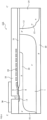
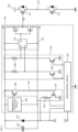
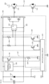
- FIG. 15 is a plan view showing the overall construction of a conventional HVIC.
- FIG. 16 is a circuit diagram showing the circuit construction of the HVIC depicted in FIG. 15 .
- the following describes an example of HVIC 100 connected to a bridge circuit 120 of a power converter and driving the first IGBT 121 at the high side of the first and second IGBTs 121 and 122 composing one phase of the bridge circuit 120 of a power converter.
- a high side gate driving circuit 101 for detecting abnormality detecting circuit 102
- abnormality detecting circuit 102 for detecting abnormality detecting circuit 102
- input/control circuit 103 for detecting abnormality detecting circuit 102
- level shift-up circuit 104 for detecting abnormality detecting circuit 102
- level shift-down circuit 107 for detecting abnormality detecting circuit 102
- HVJT high voltage junction terminating
- the high side gate driving circuit 101 and the abnormality detecting circuit 102 are disposed in the high side well region 112 and is operated with a reference potential of the emitter potential VS of the first IGBT 121 at the high side of the bridge circuit 120 of a power converter, a power supply potential of VB, and a power supply voltage of VCC'.
- the high side well region 112 is a high voltage region having a floating potential electrically isolated from the low side region 113 by the high voltage junction terminating structure 111.
- the abnormality detecting circuit 102 transmits an abnormality signal to the input/control circuit 103.
- the input/control circuit 103 is located in the low side region 113 and operates with a reference potential of GND potential.
- the input/control circuit 103 is operated with a power supply potential VCC supplied from the VCC terminal and controls the output HO of the high side gate driving circuit 101 according to a control signal HIN from an external microcontroller, for example, and an abnormality detection signal from the abnormality detecting circuit 102.
- the level shift-up circuit 104 is composed of two level shift circuits for a setting signal and for a resetting signal. Each of the two level shift circuits is composed of an n channel metal oxide semiconductor field effect transistor (nch MOSFET) 105 with a high breakdown voltage and a level shift resistor 106.
- nch MOSFET n channel metal oxide semiconductor field effect transistor
- the nch MOSFET 105 of the level shift-up circuit 104 is disposed in the high voltage junction terminating structure 111, and the level shift resistance 106 is disposed in the high side well region 112.
- the level shift-up circuit 104 converts the setting signal and resetting signal with the reference potential of the ground potential fed from the input/control circuit 103 into signals with a reference potential of the VB potential, and delivers the converted signals to a latching circuit 110 at the next stage.
- the set signal is given to turn ON the high side gate driving circuit 101 for delivering a gate signal HO to the first IGBT 121 at the high side of the bridge circuit 120 of the power converter.
- the reset signal is given to turn OFF the high side gate driving circuit 101.
- the output terminal Q of the latching circuit 110 is connected to the gate terminal of a p channel MOSFET (pch MOSFET) for charging the gate of the first IGBT 121 at the high side of the bridge circuit 120 of the power converter and to the gate terminal of an nch MOSFET for discharging the gate of the first IGBT 121.
- the level shift-down circuit 107 is composed of a high voltage pch MOSFET 108 and a level shift resistor 109.
- the pch MOSFET 108 of the level shift-down circuit 107 is disposed in the high voltage junction terminating structure 111 and the level shift resistor 109 is disposed in the low side region 113.
- the level shift-down circuit 107 transforms an abnormality detection signal with a reference potential of VB potential delivered from the abnormality detecting circuit 102 into a signal with a reference potential of the ground potential, and transmits the signal into the input/control circuit 103.
- FIG. 16 also indicates a bootstrap diode 124 and a bootstrap capacitor 125.
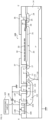
- FIG. 17 is a plan view showing in detail the planar construction around the high side well region of the HVIC of FIG. 15 .
- FIG. 17 shows only one nch MOSFET 105 of the level shift-up circuit 104 to clearly show the planar construction of the conventional HVIC 100.
- the high side well region 112 is composed of an n type diffusion region 14 and a low concentration n - type diffusion region 13 surrounding the n type diffusion region 14.
- the n - type diffusion region 13 and the n type diffusion region 14 are connected to the VB potential.
- the n - type diffusion region 13 is surrounded by the n - type diffusion region 1.
- a p - diffusion region 12 which is an isolating region.
- the n - type diffusion region 1 is surrounded by a p + type diffusion region 11 at a GND potential, which is a p + type GND region.
- a high side gate driving circuit 101 In the n type diffusion region 14 arranged are a high side gate driving circuit 101, the abnormality detecting circuit 102, and the components of the level shift-up circuit 104 including the level shift resistor 106 but excluding the nch MOSFET 105.
- the n - type diffusion region 1 arranged are the high voltage junction terminating structure 111, the nch MOSFET 105 of the level shift-up circuit 104, and the pch MOSFET 108 of the level shift-down circuit 107.
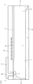
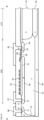
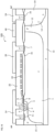
- FIG. 18 is a sectional view showing the sectional construction along the line AA-AA' indicated in FIG. 17 ;
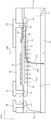
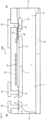
- FIG. 19 is a sectional view showing the sectional construction along the line BB-BB' indicated in FIG. 17 ;
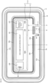
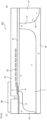
- FIG. 20 is a sectional view showing the sectional construction along the line CC-CC' indicated in FIG. 17 .
- FIG. 18 depicts the sectional construction of the nch MOSFET 105;
- FIG. 19 depicts the sectional construction of the pch MOSFET 108; and
- FIG. 20 depicts the sectional construction of the high voltage junction terminating structure 111.
- n - type diffusion region 1 is disposed in the outer peripheral side than the n type diffusion region 14, and the n - type diffusion region 1 is disposed in the outer peripheral side than the high side well region 112.
- a p - type diffusion region 15 is provided in the outer peripheral side of the substrate on the front surface layer of the substrate. The p - type diffusion region 15 penetrates in the depth direction through the n - type diffusion region 1 reaching a p type region in the back surface side of the substrate. In the p - type diffusion region 15, a p - type GND region 11 is selectively provided.
- the nch MOSFET 105 of the level shift-up circuit 104 is provided with a RESURF structure with the n - type diffusion region 1 and the p type semiconductor substrate 10, the RESURF structure being a single RESURF structure.
- the n - type diffusion region 1 also functions as a drift region.
- the impurity concentration of the n - type diffusion region 1 is about 1.0 ⁇ 10 12 /cm 2 .
- an isolation region 12 is provide between the n - type diffusion region 1 and the n - type diffusion region 13 in the deeper depth than the n - type diffusion region 1 from the front surface of the substrate.
- the isolation region 12 isolates the n - type diffusion region 1 from the n - type diffusion region 13.
- Non-patent Document 3 discloses that the optimum impurity concentration of an n - type diffusion region 1 is at most 1.4 ⁇ 10 12 /cm 2 to obtain a desired breakdown voltage for a single RESURF structure.
- the pch MOSFET 108 of the level shift-down circuit 107 has a double RESURF structure with a p type diffusion region 2, the n - type diffusion region 1, and the p type semiconductor substrate 10.
- the isolation region 12 is not provided between the n - type diffusion region 1 and the n - type diffusion region 13, and the n - type diffusion region 1 is in contact with the n - type diffusion region 13.
- the p type diffusion region 2 is formed in the front surface layer of the substrate with a depth shallower than the n - type diffusion region 1.
- the p type diffusion region 2 not only composes a double-RESURF structure, but also functions as a p type drift region.
- the impurity concentration of the p type diffusion region 2 is in the range from 5.0 ⁇ 10 11 /cm 2 to 1.0 ⁇ 10 -2 /cm 2 .
- the high voltage junction terminating structure 111 has, like the nch MOSFET 105, a single RESURF structure with the n - type diffusion region 1 and the p type semiconductor substrate 10.
- the isolation region 12 is provided between the n - type diffusion region 1 and the n - type diffusion region 13, and the n - type diffusion region 1 is isolated from the n - type diffusion region 13 by the isolation region 12.
- the symbols 3, 4, 5, 7, 8, and 9 represent the components composing a structure of MOS gate structure, which is an insulated gate structure comprising a metal-oxide film-semiconductor gate, of the nch MOSFET 105.
- the symbol 16 in FIG. 18 indicates a contact, which is an electrical contact region, between a VB electrode 39 and the n type diffusion region 14.
- the symbols 24, 25, 27, 28, and 29 (in FIG. 19 ) represent the components composing the MOS gate structure of the pch MOSFET 108.
- the symbols 34 and 35 represent a source electrode and a drain electrode of the nch MOSFET 105, respectively.
- the symbols 36 and 37 (in FIG. 19 ) represent a source electrode and a drain electrode of the pch MOSFET 108.
- the symbols 38 (in FIG. 19 ) and 40 (in FIG. 18 ) represent a GND electrode and a field plate, respectively.
- a control signal from a microcontroller, for example, given to the input/control circuit 103 is transmitted to the high side gate driving circuit 101 to drive the first IGBT 121 at the high side, for example, connected to the conventional HVIC 100, of the first IGBT 121 and the second IGBT 122 composing one phase of the bridge circuit 120 of a power converter.
- the abnormality detecting circuit 102 detects any abnormality such as over-current or over-heating, the abnormality detecting circuit 102 transmits an abnormality signal to the input/control circuit 103, and the first IGBT 121 at the high side is turned OFF and the abnormality is notified to the microcontroller.
- the high side gate driving circuit 101 is operated on a reference potential of the emitter potential VS of the first IGBT 121 at the high side of the bridge-connected circuit, wherein the potential VS is the potential at the node 123 between the first IGBT 121 and the second IGBT 122 at the low side.
- the reference potential of the high side gate driving circuit 101 rises to several hundred volts at the maximum above the reference potential, which is the ground potential, of the input/control circuit 103.
- the high voltage junction terminating structure 111 holds a breakdown voltage between the high side gate driving circuit 101 and the input/control circuit 103.
- Non-patent Document 4 discloses an area-effective 600 V p-channel level shifter using a self-isolation structure without degradation of blocking capability.
- Patent Document 2 discloses a HVIC of this type.
- This HVIC has a three layer structure comprising a first region of a first conductivity type, a second region of a second conductivity type formed selectively in the surface layer of the first principal surface of the first region, and a third region of the first conductivity type formed selectively in the surface layer of the second region.
- the net doping amount of the second region is in the range from 1 ⁇ 10 11 /cm 2 to 4 ⁇ 10 12 /cm 2 so that the depletion layer extending to both sides of a first pn junction between the first region and the second region and the depletion layer extending to both sides of a second pn junction between the second region and the third region are united in the second region, when both the first pn junction and the second pn junction are reversely biased.
- the net doping amount of the third region is in the range from 1 ⁇ 10 11 /cm 2 to 2 ⁇ 10 12 /cm 2 so that the depletion layer extending to both sides of the second pn junction reaches the surface of the third region.
- the HVIC further comprises, inside an area surrounded by the third region, a second conductivity type region electrically connected to the second region, a first conductivity type region selectively formed in the surface layer of the second conductivity type region, a first conductivity type channel MIS transistor formed in the surface layer of the second conductivity type region, and a second conductivity type channel MIS transistor formed in the surface layer of the first conductivity type region.
- Patent Document 3 discloses another HVIC.
- This HVIC comprises: a semiconductor material layer of a first conductivity type disposed on a semiconductor substrate and having an upper surface subjected to doping treatment, a base region of a second conductivity type formed in the surface region of the semiconductor material layer to a predetermined depth and having substantially a semicircular shape, a source region of the first conductivity type formed in the base region and forming a surface channel region between the source region and the semiconductor material layer, a source electrode in contact with the source region and electrically connected to a low voltage reference control circuit, a gate insulating layer disposed so as to be in contact with the source region and a part of the upper surface of the surface channel region, a conductive gate layer disposed in the gate insulating layer, a drain region formed in the upper surface region of the semiconductor material layer at a position laterally apart from the base region, a drain electrode formed on the drain region and in contact with a part of the upper surface of the semiconductor material layer, a contact electrode in contact with another part
- Patent Document 4 discloses still another HVIC.
- the HVIC comprises: a first region of a p type semiconductor substrate, an n type second region selectively formed in the surface layer of the first region, a p type third region selectively formed in the surface layer of the second region, an n type fifth region selectively formed in the surface layer of the second region, a p type sixth region selectively formed in the surface layer of the third region, a pch MOSFET formed in the surface layer of the second region, an nch MOSFET formed in the surface layer of the third region, and a high voltage junction terminating structure provided surrounding the first region.
- Patent Document 5 discloses a high-voltage integrated circuit, HVIC, the HVIC comprising: a high side gate driving circuit disposed in a high side well region of the second conductivity type, an input/control circuit located in a low side region, a level shift-up circuit, a level shift-down circuit and a high voltage junction terminating, HVJT, structure isolating the high side well region from the low side region; wherein the high side well region is surrounded by a first semiconductor region of a second conductivity type disposed on a semiconductor substrate of a first conductivity type or formed on a surface layer of the semiconductor substrate of the first conductivity type, wherein the high side well region is adjacent to the first semiconductor region and disposed on the semiconductor substrate; the level shift-down circuit comprising: a first field effect transistor of a first conductivity type that comprises: the first semiconductor region, a second semiconductor region of a first conductivity type selectively formed on a surface layer of the first semiconductor region, a third semiconductor region of the first conductivity type selectively formed on
- the conventional HVIC 100 described above referring to FIG. 15 and FIG. 16 has the following problems.
- the conventional HVIC 100 employs a single RESURF structure in the nch MOSFET 105 and in the high voltage junction terminating structure 111 composed of the n - type diffusion layer 1 and the p type semiconductor substrate 10
- the pch MOSFET 108 employs a double RESURF structure composed of the p type diffusion region 2, the n - type diffusion region 1, and the p type semiconductor substrate 10.
- the optimum condition for the n - type diffusion region 1 differs for the pch MOSFET 108, and for the nch MOSFET 105 and the high voltage junction terminating structure 111.
- the optimum impurity concentration of the n - type diffusion region 1 to obtain a desired breakdown voltage is at most 1.4 ⁇ 10 12 /cm 2 for a single RESURF structure. An impurity concentration higher than this value cannot ensure sufficient breakdown voltage.
- the optimum impurity concentration of the n - type diffusion region 1 to ensure the breakdown voltage between the p type diffusion region 2 and the n - type diffusion region 1 is at most 2.8 ⁇ 10 12 /cm 2 .
- an impurity concentration of the p type diffusion region is at most 1.4 ⁇ 10 12 /m 2 and at the same time it is necessary that the difference between the impurity concentrations in the p type diffusion region 2 and in the n - type diffusion region 1 is at most 1.4 ⁇ 10 12 /cm 2 .
- These conditions for the impurity concentration of the p type diffusion region 2 is necessary conditions to obtain a desired breakdown voltage and not a sufficient condition.
- optimization is needed to the impurity concentration of the p type diffusion region 2 while satisfying the above-mentioned necessary conditions.
- the optimum impurity concentration of the p type diffusion region 2 depends on the impurity concentration of the n - type diffusion region 1; a low impurity concentration for the n - type diffusion region 1 leads to lower optimum impurity concentration of the p type diffusion region 2.
- a lower impurity concentration of the n - type diffusion region 1 tends to lower the optimum impurity concentration of the p type diffusion region 2 because the amount of positive space charges in the depletion layer has to be balanced with the amount of negative space charges. Therefore, a low impurity concentration of the n - type diffusion region 1 means a small amount of positive space charges, which are donors, in the n - type diffusion region 1, reducing the negative space charges, which are acceptors, allowed in the depletion layer of the p type diffusion region 2.
- the impurity concentration in the p type diffusion region 2 is higher than the impurity concentration of the n - type diffusion region 1, deficiency of the positive space charges causes incomplete depletion of the p type diffusion region 2, resulting in insufficient breakdown voltage.
- Negative space charges in a depletion layer exist not only in the depletion layer extending from pn junction between the p type diffusion region 2 and the n - diffusion region 1 into the p type diffusion region 2, but also exist in an approximately same amount in the depletion layer extending from the pn junction between the p type semiconductor substrate and the n - type diffusion region 1 into the p type semiconductor substrate. Consequently, in order to make the p type diffusion region 2 thoroughly depleted, the amount of the positive space charges in the n - type diffusion region 1 has to be about twice the amount of the negative space charges in the p type diffusion region 2. Therefore, the optimum impurity concentration in the p type diffusion region 2 for ensuring a sufficient breakdown voltage is about half the impurity concentration in the n - type diffusion region 1.
- a design condition to ensure a sufficient breakdown voltage in the nch MOSFET 105 and the high voltage junction terminating structure 111 with a single RESURF structure is that an impurity concentration Nd per unit area of the n - diffusion region 1 (hereinafter referred to simply as an impurity concentration of the n - diffusion region 1) is at most 1.4 ⁇ 10 12 /cm 2 , or the inequality Nd ⁇ 1.4 ⁇ 10 -2 /cm 2 holds.
- a double RESURF condition for the pch MOSFET 108 with a double RESURF structure to ensure a sufficient breakdown voltage is to satisfy the following four conditions.
- the first condition is that the impurity concentration Nd of the n - type diffusion region 1 is about twice the impurity concentration Na of the p type diffusion region 2, or Nd ⁇ 2 ⁇ Na.
- the second condition is that the impurity concentration Na of the p type diffusion region 2 is at most 1.4 ⁇ 10 12 /cm 2 (Na ⁇ 1.4 ⁇ 10 12 /cm 2 ).
- the third condition is that the impurity concentration Nd of the n - type diffusion region 1 is at most 2.8 ⁇ 10 12 /cm 2 (Nd ⁇ 2.8 ⁇ 10 12 /cm 2 ) .
- the fourth condition is that the difference between the impurity concentration Nd of the n - type diffusion region 1 and the impurity concentration Na of the p type diffusion region 2 is at most 1.4 ⁇ 10 12 /cm 2 (Nd - Na ⁇ 1.4 ⁇ 10 12 /cm 2 ) .
- the condition for ensure a sufficient breakdown voltage is to satisfy both the single RESURF condition and the double RESURF condition. More specifically, both the single RESURF condition and the double RESURF condition are satisfied when the following two conditions are satisfied: firstly, the impurity concentration Nd of the n - type diffusion region 1 is at most 1.4 ⁇ 10 12 /cm 2 (Nd ⁇ 1.4 ⁇ 10 12 /cm 2 ); secondly, the impurity concentration Na of the p type diffusion region 2 is at most 7.0 ⁇ 10 11 /cm 2 (Na ⁇ 7.0 ⁇ 10 11 /cm 2 ) .
- the impurity concentration Nd of the n - type diffusion region 1 needs to be at most 1.4 ⁇ 10 12 /cm 2 .
- the impurity concentration Na of the p type diffusion region 2 is necessarily at most 7.0 ⁇ 10 11 /cm 2 .
- the impurity concentration Na of the p type diffusion region 2 is at a value approximately 7.0 ⁇ 10 11 /cm 2 , the pch MOSFET 108 cannot have a sufficient current carrying capacity because of the problems of a high drift resistance in the p type diffusion region 2 and the pinch-off of the p type diffusion region 2.
- the impurity concentration Na of the p type diffusion region 2 is raised in order for the pch MOSFET 108 with a double RESURF structure to exhibit sufficiently high current carrying capacity, the pch MOSFET 108 cannot have a sufficiently high breakdown voltage.
- the conventional HVIC 100 is hardly provide optimum condition for both the current carrying capacity and breakdown voltage of the pch MOSFET 108.
- the impurity concentration Nd of the n - type diffusion region 1 is a low value of about 1.0 ⁇ 10 12 /cm 2
- an electric field is generated in the direction from the p type diffusion region 2 toward the p type semiconductor substrate 10, creating a leakage current to the p type semiconductor substrate 10.
- a breakdown voltage is hardly ensured between the p type diffusion region 2 and the p type semiconductor substrate 10.
- the impurity concentration Nd of the n - type diffusion region 1 in the pch MOSFET 108 is necessarily at least 1.3 ⁇ 10 12 /cm 2 . Because a p type diffusion region 2 is formed on the surface of the n - type diffusion region 1 of the pch MOSFET 108, the impurity concentration of the n - type diffusion region 1 of the pch MOSFET, when formed by ion implantation homogeneous over the surface as usual, becomes lower than those of the n - diffusion regions 1 of the nch MOSFET 105 and the high voltage junction terminating structure 111.
- the impurity concentration of the n - type diffusion region 1 of the pch MOSFET 108 is lower by more than 10 % than the impurity concentration of the nch MOSFET 105 and the n - type diffusion region 1 of the high voltage junction terminating structure 111.
- the impurity concentration of the n - type diffusion region 1 of the nch MOSFET 105 and the impurity concentration of the n - type diffusion reign 1 of the high voltage junction terminating structure 111 are set at the upper limit value of 1.4 ⁇ 10 12 /cm 2 , the impurity concentration of the n - type diffusion region 1 of the pch MOSFET 108 becomes lower than 1.3 ⁇ 10 12 /cm 2 .
- the ion implantation processes are carried out separately for the n - type diffusion region 1 for the pch MOSFET 108, and for the nch MOSFET 105 and the high voltage junction terminating structure 111. This causes increased process cost.
- Non-patent Document 1 discloses a method of increasing the impurity concentration of the p type diffusion region 2 keeping a sufficient breakdown voltage to ensure a high current carrying capacity of the pch MOSFET 108 while maintaining the high breakdown voltage. This is achieved by a p type diffusion region 2 in a configuration of stripes for easy depletion. This method of the Non-patent Document 1, however, decreases the area of the drift region of p type diffusion region 2.
- the channel width of the pch MOSFET 108 needs to be sufficiently large, wherein the channel width is a width, in the direction perpendicular to the direction from a p + type drain region 27 to the source region, of the channel, or a p type inversion layer generated in the n - diffusion region 1 at the place between a source region of a p type diffusion region 24 and a drift region of the p type diffusion region 2 in an ON state.
- the enlarged channel width of the pch MOSFET 108 causes a large parasitic capacitance of the pch MOSFET 108, which increases the displacement current associated with dV/dt surge voltage, which may cause malfunctioning of the HVIC.
- Non-patent Document 2 discloses a method for ensuring a high breakdown voltage between the p type diffusion region 2 and the p type semiconductor substrate 10 in a structure having the p type diffusion region 2 of a stripe shape.
- the Document fails to disclose a method for ensuring a high breakdown voltage between the p type diffusion region 2 and the p type semiconductor substrate 10 in a structure having the p type diffusion region 2 of a conventional structure without a stripe shape.
- the present invention has been made to solve the above-described problems of the conventional technologies and an object of the present invention is to provide a semiconductor device, which has a high voltage junction terminating structure and a high voltage p-channel insulated gate type field effect transistor on a single chip, the semiconductor device ensuring optimum condition for a high breakdown voltage of the semiconductor device and a large current carrying capacity of the p-channel insulated gate type field effect transistor.
- the HVIC further comprises a bipolar transistor that comprises: a sixth semiconductor region of the second conductivity type, a seventh semiconductor region of the first conductivity type, an eighth semiconductor region of the second conductivity type, a third electrode, and a fourth electrode.
- the sixth semiconductor region is selectively formed in a surface layer of the first semiconductor region, separated from the first semiconductor region by a twelfth semiconductor region of the first conductivity type and separated from the second semiconductor region.
- the seventh semiconductor region is selectively formed within the sixth semiconductor region.
- the seventh semiconductor region is connected to the second electrode.
- the eighth semiconductor region is selectively formed within the seventh semiconductor region.
- the eighth semiconductor region is at a potential of the semiconductor substrate.
- the third electrode is in contact with the sixth semiconductor region.
- the fourth electrode is in contact with the eighth semiconductor region.
- a power supply potential electrode at a higher potential than the semiconductor substrate is provided.
- a resistor electrically connected to a node between the third electrode and the power supply potential electrode is provided.
- the distance between the second semiconductor region and the fifth semiconductor region is at most 5 ⁇ m.
- the distance between the second semiconductor region and the fifth semiconductor region is in the range from 3 ⁇ m to 10 ⁇ m.
- the second semiconductor region and the fifth semiconductor region have substantially the same impurity concentration.
- a semiconductor device of the present invention provides a semiconductor device that has a high voltage junction terminating structure and a high voltage p-channel insulated gate type field effect transistor on a single chip and ensures optimum condition for a high breakdown voltage of the semiconductor device and a large current carrying capacity of the p-channel insulated gate type field effect transistor.
- the HVIC of the First Embodiment comprises, in a single semiconductor chip, a high side gate driving circuit 101, an abnormality detecting circuit 102, an input/control circuit 103, a level shift-up circuit 104, a level shift-down circuit 107, and a high voltage junction terminating (HVJT) structure 111, as shown in FIG. 15 .
- the HVIC drives, for example, a first IGBT 121 of the first and second IGBTs 121 and 122 composing one phase of a bridge circuit 120 of a power converter, as shown in FIG. 16 .
- the HVIC of First Embodiment differs from the conventional HVIC 100 in that the high voltage junction terminating structure 111 and the nch MOSFET105, which is a field effect transistor of a second conductivity type, of the level shift-up circuit 104 have, like the pch MOSFET 108, which is a first field effect transistor of a first conductivity type, of the level shift-down circuit 107, a double RESURF structure with a first p type diffusion region 2a, which is a fifth semiconductor region, provided in the n - type diffusion region 1, which is a first semiconductor region.
- FIG. 1 is a planar view showing a planar construction of the HVIC of First Embodiment.
- FIG. 1 shows in detail a planar construction of the peripheral portion of the high side well region 112.
- FIG. 10 and FIG. 12 also show planar constructions of other high side well regions in detail.
- n - type diffusion region 1 composing a high voltage junction terminating structure 111, an n - diffusion region 13 and an n type diffusion region 14 composing the high side well region 112, and a not depicted low side region.
- the n type diffusion region 14 can accommodate a high side gate driving circuit 101, an abnormality detecting circuit 102, and a level shift-up circuit 104 including a level shift resistor 106 but excluding an nch MOSFET 105.
- the n - type diffusion region 13 surrounds the n type diffusion region 14.
- the n - type diffusion region 13 and the n type diffusion region 14 are connected to a VB potential, which is the highest potential of the high side well region 112.
- the n - type diffusion region 1 is a high voltage region electrically isolated from a low side region by a p + GND region 11, which is described later, and disposed surrounding the n - type diffusion region 13.
- the n - type diffusion region 13 is selectively isolated from the n - type diffusion region 1, for example, by a p - type diffusion region 12, which is an isolating region, having a ring planar shape with roughly a shape of the letter C.
- the high side well region 112, which includes the n - type diffusion region 13 and the n type diffusion region 14, is electrically isolated from the n - type diffusion region 1 at the place of the isolating region 12.
- the isolation between the high side well region 112 and the n - type diffusion region 1 by the isolation region 12 reduces the leakage current from the n type diffusion region 14 to the n - type diffusion region 1 upon turning ON of the nch MOSFET 105.
- an nch MOSFET 105 of the level shift-up circuit 104 and the high voltage junction terminating structure 111 are provided in the portion of the n - type diffusion region 1 that is isolated from the high side well region 112 by the isolating region 12.
- a pch MOSFET 108 of the level shift-down circuit 107 is disposed in the portion of the n - type diffusion region 1 that is in contact with the n - type diffusion region 13.
- the nch MOSFET 105 and the pch MOSFET 108 are preferably disposed as distant as possible from circuits arranged on the low side region in order to avoid interference in signal transmission.
- FIG. 1 shows only a single nch MOSFE 105 of the level shift-up circuit 104
- another nch MOSFET 105 is also disposed in the portion of the n - type diffusion region 1 that is isolated from the high side well region 112 by the isolation region 12.
- the high voltage junction terminating structure 111 is depicted as a part between the nch MOSFET 105 and the pch MOSFET 108
- the whole part in the n - type diffusion region 1 is the high voltage junction terminating structure 111 excepting the portions of the nch MOSFET 105 and the pch MOSFET 108.
- the nch MOSFET 105 and the pch MOSFET 108 are incorporated together in the high voltage junction terminating structure 111.
- a first p type diffusion region 2a and a second p type diffusion region 2b are provided composing a double RESURF structure over the almost whole region of the n - type diffusion region 1. More specifically, the first p type diffusion region 2a is disposed over the portion of the n - type diffusion region 1 in which the nch MOSFET 105 and the high voltage junction terminating structure 111 are disposed.
- the second p type diffusion region 2b which is a second semiconductor region, is disposed on the portion of the n - type diffusion region 1 in which the pch MOSFET 108 is disposed, the second p type diffusion region 2b being separated from the first p type diffusion region 2a.
- the first p type diffusion region 2a and the second p type diffusion region 2b are disposed with a predetermined gap w between the two and are separated by the portion of the n - type diffusion region 1 exposing to the front surface of the substrate between the first p type diffusion region 2a and the second p type diffusion region 2b.
- the first p type diffusion region 2a and the second p type diffusion region 2b are preferably formed with the same conditions of, for example, a diffusion depth and an impurity concentration. This is because the same conditions can provide the same double RESURF conditions for the nch MOSFET 105, the pch MOSFET 108, and the high voltage junction terminating structure 111.
- the gap w between the first p type diffusion region 2a and the second p type diffusion region 2b is preferably in the region from 3 ⁇ m to 10 um.
- the reason for this dimension is as follows.
- a p + type source region 25, which is a third semiconductor region, of the pch MOSFET 108 is disposed at the substrate center side, which is the side of the high side well region 112, of the second p type diffusion region 2b and faces to the second p type diffusion region 2b interposing the n - type diffusion region 1.
- the p + type source region 25 can be disposed near a joining surface between the n - type diffusion region 1 and the n type diffusion region 13, the joining surface being at the place of interruption of the isolation region 12 with a roughly C shape.
- a p + type drain region 27, which is a fourth semiconductor region, of the pch MOSFET 108 is disposed at the outer peripheral side, which is the low side region side, in the second p type diffusion region 2b.
- the drain current of the pch MOSFET 108 in an ON state thereof flows from the p + source region 25 through the second p type diffusion region 2b to the p + type drain region 27.
- the drain current flowing from the p + type source region 25 through the second p type diffusion region 2b to the p + type drain region 27 flows aside from the second p type diffusion region 2b or from the p + type drain region 27 through the n - type diffusion region 1 into the first p type diffusion region 2a and punches-through under the first p type diffusion region 2a, to a p type region in the back surface side of the substrate, generating a leakage current.
- This p type region in the back surface side of the substrate is a p type region of the semiconductor substrate 10 remained in the deeper region than the n - type diffusion region 1 without forming the n - type diffusion region 1.
- the gap w between the first p type diffusion region 2a and the second p type diffusion region 2b is larger than 10 um, the portion of the n - type diffusion region 1 located between the first p type diffusion region 2a and the second diffusion region 2b cannot be completely depleted, making it difficult to ensure a predetermined breakdown voltage. Therefore, the gap w between the first p type diffusion region and the second diffusion region 2b is preferably in the range of 3 ⁇ m to 10 ⁇ m.
- the high side well region 112 including the n - type diffusion region 13 and the n type diffusion region 14, and the n - type diffusion region 1, which is a high voltage region, are surrounded by a p - type diffusion region 15 and a p + type diffusion region 11, which is a p + type GND region, disposed in the p - type diffusion region 15, and thus are electrically isolated from the low side region (not depicted) at a lower potential than the high side well region 112.
- the p - type diffusion region 15 is in contact with the first p type diffusion region 2a and without contact with the second diffusion region 2b.
- the p - type diffusion region 15 is isolated from the second p type diffusion region 2b by the n - type diffusion region 1 that is exposed to the front surface of the substrate between the p - type diffusion region 15 and the second p type diffusion region 2b.
- Within the p - type diffusion region 15 provided are a plurality of n + type source regions 5 and p + type contact regions 6 of nch MOSFETs 105.
- n + type source regions 5 and the p + type contact regions 6 are disposed alternately and repeatedly along the joint surface between the first p type diffusion region 2a and the p - type diffusion region 15.
- a part of the n - type diffusion region 1 is exposed to the front surface of the substrate between the p - type diffusion region 15 and the first p type diffusion region 2a. That is, a planar pattern of the part of the first p type diffusion region 2a opposing to the n + type source region 5 and the p + type contact region 6 is a pattern where the n - type diffusion region 1 and the first p type diffusion region 2a are alternately and repeatedly arranged.
- n + type drain region 7 of the nch MOSFET 105 is disposed in the central side of the first p type diffusion region 2a, opposing to the n + type source region 5 and the p + type contact region 6 interposing the first p type diffusion region 2a.
- FIG. 2 is a sectional view showing the sectional construction along the line A-A' in FIG. 1 ;
- FIG 3 is a sectional view showing the sectional construction along the line B-B' in FIG. 1 ;
- FIG. 4 is a sectional view showing the sectional construction along the line C-C' in FIG. 1 ;
- FIG. 5 is a sectional view showing the sectional construction along the line D-D' in FIG. 1 .
- FIG. 2 illustrates a sectional construction of the nch MOSFET 105;
- FIG. 3 illustrates a sectional construction of the pch MOSFET 108;
- FIG. 4 illustrates a sectional construction of the high voltage junction terminating structure 111; and FIG. 5 illustrates a sectional construction of the portion of the n - type diffusion region 1 interposed between the first p type diffusion region 2a and the second p type diffusion region 2b.
- the n - type diffusion region 1, and the n - type diffusion region 13 and the n type diffusion region 14 composing the high side well region 112 are selectively formed in the surface layer on the front surface of the p type semiconductor substrate 10.
- the n - type diffusion region 13 is disposed in the outer peripheral side of the substrate than the n type diffusion region 14.
- the n - type diffusion region 13 is disposed in outer peripheral side of the n - type diffusion region 13, which means outer peripheral side of the high side well region 112.
- the p - type diffusion region 15 is provided in the surface layer of the n - type diffusion region 1 in the front surface side of the substrate in the peripheral side of the substrate.
- the p - type diffusion region 15 extends in the depth direction through the n - type diffusion region 1 reaching a p type region in the back surface side of the substrate.
- the p - type diffusion region 15 extends toward the central part of the substrate with a shallower depth than the n - type diffusion region 1.
- a p + type GND region 11 is selectively formed in the shallow region of the central side of the substrate of the p type diffusion region 15.
- the nch MOSFET 105 of the level shift-up circuit 104 has a double RESURF structure comprising the first p type diffusion region 2a, the n - type diffusion region 1 and the p type semiconductor substrates 10, which is a semiconductor chip.
- the n - type diffusion region 1 simultaneously serves as an n - type drift region.
- An isolation region 12 is provided between the n - type diffusion region 1 and the n - type diffusion region 13 from the front surface of the substrate with a depth deeper than the n - type diffusion region 1.
- the isolation region 12 isolates the n - type diffusion region 1 from the n - type diffusion region 13.
- the reason for the isolation between the n - type diffusion region 1 and the n - type diffusion region 13 by the isolation region 12 in the nch MOSFET 105 is that the drain potential of the nch MOSFET 105 and the VB potential, which is the highest potential in the high side well region 112, have to be isolated from each other in order to flow a current through the level shift resistor 106 in the level shift-up circuit 104.
- the p type base region 3 is in contact with the p - type diffusion region 15.
- An n type diffusion region 4 is provided between the p type base region 3 and the n + type source region 5.
- the first p type diffusion region 2a is provided in the surface layer of the n - type diffusion region 1 in the front surface side of the substrate with a depth shallower than the n - type diffusion region 1.
- the first p type diffusion region 2a is disposed between the p type base region 3 and the n + type drain region 7 separated away from the p type base region 3 and the n + type drain region 7.
- a LOCOS (local oxidation of silicon) film 31 is provided on the surface of the first p type diffusion region 2a and over the surface of the n - type diffusion region 1 at the place between the first p type diffusion region 2a and the n + type drain region 7.
- the LOCOS film 31 is also provided on the part of the n - type diffusion region 1 in the central side of the n + type drain region 7 and on the substrate surface in the high side well region 112 side.
- the gate electrode 9 is extending over the LOCOS film 31 covering the first p type diffusion region 2a.
- a resistor 33 which is a resistive field plate that functions as a field plate, is provided at a position opposing to the first p type diffusion region 2a in the depth direction.
- the resistive field plate 33 is arranged, for example, in a spiral planar pattern surrounding the high side well region 112.
- a source electrode 34 which is a fifth electrode, is in contact with the n + source region 5, the n + type contact region, and the p + type GND region 11 through a contact hole penetrating through the interlayer dielectric film 32 in the depth direction.
- a drain electrode 35 which is a sixth electrode, is in contact with the n + type drain region 7 through a contact hole penetrating through the interlayer dielectric film 32 in the depth direction.
- the pch MOSFET 108 of the level shift-down circuit 107 has a double RESURF structure comprising the second p type diffusion region 2b, the n - type diffusion region 1, and the p type semiconductor substrate 10.
- the source electrode 36 is connected to the VB potential that is the highest potential of the high side well region 112, so that the pch MOSFET 108 has a construction where the n - type diffusion region 1 is in contact with the n - type diffusion region 13.
- a p type diffusion region 24 is provided at a place in the central side of the substrate than the p - type diffusion region 15.
- a p + type source region 25 is provided in the p type diffusion region 24.
- the second p type diffusion region 2b is provided in the surface layer of the n - type diffusion region 1 in the front surface side of the substrate with a depth shallower than the n - type diffusion region 1.
- the second p type diffusion region 2b is disposed between the p type diffusion region 24, or a p + type source region 25, and the p - type diffusion region 15 separated from the p type diffusion region 24 and the p - type diffusion region 15.
- the second diffusion region 2b not only composes a double RESURF structure, but also functions as a p type drift region.
- a p + type drain region 27 is provided in the side of the p - type diffusion region 15.
- the p + type drain region 27 is isolated from the p - type diffusion region 15 by the n - type diffusion region 1.
- the p + type drain region 27 is isolated from the p - type diffusion region 15 because the drain potential of the pch MOSFET 108 has to be isolated from the ground potential in order to flow a current through the level shift resistor 109 of the level shift-down circuit 107.
- a LOCOS film 31 is provided on the surface of the second p type diffusion region 2b excepting the place of exposing p + type drain region 27.
- the LOCOS film 31 is also provided on the substrate surface in the n type diffusion region 14 side from the p + type source region 25.
- the gate electrode 29 is extending over the LOCOS film 31 covering the second p type diffusion region 2b.
- a resistive field plate 33 is provided at the place opposing the second p type diffusion region 2b in the depth direction.
- a source electrode 36 which is a first electrode, is in contact with the p + type source region 25 through a contact hole penetrating in the depth direction through the interlayer dielectric film 32.
- a drain electrode 37 which is a second electrode, is in contact with the p + type drain region 27 through a contact hole penetrating in the depth direction through the interlayer dielectric film 32.
- a GND electrode 38 is in contact with the p + type GND region 11.
- the high voltage junction terminating structure 111 like the nch MOSFET 105, has a double RESURF structure comprising the first p type diffusion region 2a, the n - type diffusion region 1, and the p type semiconductor substrate 10, which is a semiconductor chip.
- An isolation region 12 is provided between the n - type diffusion region 1 and the n - type diffusion region 13, and the isolation region 12 isolates the n - type diffusion region 1 from the n - type diffusion region 13.
- the reason for the isolation between the n - type diffusion region 1 and the n - type diffusion region 13 in the high voltage junction terminating structure 111 is as follows.
- the part of the n - type diffusion region 1 composing the high voltage junction terminating structure 111 and the part of the n - type diffusion region 1 composing the n - drift region of the nch MOSFET 105 are linked to each other. Consequently, if the n - type diffusion region 1 is in contact with the n - type diffusion region 13 in the high voltage junction terminating structure 111, a leakage current would flow from the VB electrode 39 to the drain electrode 35 of the nch MOSFET 105 through the n - type diffusion region 1. Therefore, the n - type diffusion region 1 and the n - type diffusion region 13 are isolated from each other.
- the first p type diffusion region 2a is in contact with the p - type diffusion region 15.
- the part of the n - diffusion region 1 between the first p type diffusion region 2a and the second p type diffusion region 2b composes a RESURF structure with the n - type diffusion region 1 and the p type semiconductor substrate 10.
- an isolation region is not provided between the n - diffusion region 1 and the n - type diffusion region 13, and the n - diffusion region 1 and the n - type diffusion region 13 are in contact with each other.
- the surface of the n - diffusion region 1 is covered with a LOCOS film 31.
- Numerical values of the dimensions and impurity concentrations in the HVIC of First Embodiment can be as follows.
- the length L, or the width, of the LOCOS film 31 covering the second p type diffusion region 2b in the direction from the p + source region 25 to the p + type drain region 27 of the pch MOSFET 108 can be in the range from 100 ⁇ m to 200 ⁇ m, for example.
- the resistivity of the p type semiconductor substrate 10 is in the range from 100 Q cm to 400 ⁇ cm, for example.
- the impurity concentration per unit area Nd of the n - type diffusion region 1 (hereinafter referred to simply as an impurity concentration of the n - type diffusion region 1), the n - type diffusion region 1 composing the nch MOSFET 105, the pch MOSFET 108, and the high voltage junction terminating structure 111, has a common value independent on these semiconductor devices and is determined to ensure a sufficient breakdown voltage and ensure sufficient current carrying capacity of the pch MOSFET 108.
- the impurity concentration per unit area Na (hereinafter referred to simply as an impurity concentration of the first p type diffusion region 2a and of the second p type diffusion region 2b) of the first p type diffusion region 2a composing the nch MOSFET 105 and the high voltage junction terminating structure 111 and of the second p type diffusion region 2b composing the pch MOSFET 108 also has a common value independent on these semiconductor devices and is determined to ensure a sufficient breakdown voltage and ensure sufficient current carrying capacity of the pch MOSFET 108. More specifically, the impurity concentration Nd of the n - type diffusion region 1 is preferably in the range from 1.3 ⁇ 10 12 / cm 2 to 2.8 ⁇ 10 12 / cm 2 , for example.
- the impurity concentration Na of the first p type diffusion region 2a and the second p type diffusion region 2b (hereinafter, the first p type diffusion region 2a and the second p type diffusion region 2b are also called commonly as a p type diffusion region 2.) is preferably in the rage from 1.1 ⁇ 10 12 / cm 2 to 1.4 ⁇ 10 12 / cm 2 , for example.
- the upper limit value of the impurity concentration Nd of the n - type diffusion region 1 and the impurity concentration Na of the p type diffusion region 2 are determined based on the design condition of the double RESURF structure (a double RESUFR condition) when the n - type diffusion region 1 and the p type diffusion region 2 are completely depleted. As described previously, the double RESURF conditions are the following four conditions.
- a first condition is that the impurity concentration Nd of the n - type diffusion region 1 is larger than the impurity concentration per unit area Na of the p type diffusion region 2 (herein after referred to as an impurity concentration of the p type diffusion region 2) and a value about twice the impurity concentration Na of the p type diffusion region 2: Nd > Na and Nd ⁇ 2 ⁇ Na.
- a second condition is that the impurity concentration Na of the p type diffusion region 2 is at most 1.4 ⁇ 10 12 / cm 2 : Na ⁇ 1.4 ⁇ 10 12 / cm 2 .
- a third condition is that the impurity concentration Nd of the n - type diffusion region 1 is at most 2.8 ⁇ 10 12 / cm 2 : Nd ⁇ 2.8 ⁇ 10 12 / cm 2 .
- a fourth condition is that the difference between the impurity concentration Nd of the n - type diffusion region 1 and the impurity concentration Na of the p type diffusion region 2 is at most 1.4 ⁇ 10 12 / cm 2 : Nd - Na ⁇ 1.4 ⁇ 10 12 / cm 2 .
- the lower limit value of the impurity concentration Nd of the n - type diffusion region 1 is determined based on the breakdown voltage in the depth direction, or vertical direction, (hereinafter referred to as a vertical breakdown voltage) required between the p type diffusion region 2 and the p type semiconductor substrate 10. The following describe in detail about a calculation method of the lower limit of the impurity concentration Nd of the n - type diffusion region 1.
- FIG. 6 is a sectional view showing generation of leakage current in a pch MOSFET of a conventional HVIC.
- FIG. 7 shows a voltage-current characteristics of the HVIC depicted in FIG. 6 .
- FIG. 8 shows abnormal output characteristics caused by the pinch-off of the drift region, which is the second p type diffusion region 2b, in the pch MOSFET 108 of the HVIC depicted in FIG. 6 ;
- an electric field 41a develops in the direction from the semiconductor substrate 10 toward the second p type diffusion region 2b at the pn junction between the n - type diffusion region 1 and the second p type diffusion region 2b.
- the electric field 41a is indicated by the arrows in the negative y-axis direction, or upward direction.
- an electric field 41b in the direction from the second p type diffusion region 2b toward the p type semiconductor substrate 10 is generated at least in a portion of the pn junction between the n- type diffusion region 1 and the second p type diffusion region 2b.
- the electric field 41b is indicated by the arrows in the positive y-axis direction, or downward direction.
- the electric field 41b in the direction from the second p type diffusion region 2b toward the p type semiconductor substrate 10 adversely affects the source-drain current 42 from the p + source region 25 through the second p type diffusion region 2b to the p + drain region 27 to leak to the n - type diffusion region 1 and the p type semiconductor substrate 10.
- a leakage current 43 from the second p type diffusion region 2b toward the p type semiconductor substrate 10 is generated, or punch through occurs.
- the current Id flowing through the p + type drain region 27, which is dominated by hole current becomes smaller than the current Is flowing through the p - type source region 25.
- the current I sub flowing to the p type semiconductor substrate 10 increases.
- the current I sub is equal to the amount of decrease in the current Id.
- FIG. 8 shows relationship between the source-drain voltage V ds and the source-drain current Ids for the varied gate voltages Vg from zero volts to 15 volts with a step of one volt applied to the pch MOSFET 108.
- the source-drain voltage Vds for a leakage current 43 to occur is the allowed maximum voltage BV pt in the depth direction, that is a vertical breakdown voltage, and given approximately by the formula (1) below.
- the formula (1) is obtained by deriving the source-drain voltage Vds using Poisson equation, when the electric field 41b in the direction from the second p type diffusion region 2b toward the p type semiconductor substrate 10 is generated at the pn junction between the n - type diffusion region 1 and the second p type diffusion region 2b.
- n sub is an impurity concentration per unit volume of the p type semiconductor substrate 10 (hereinafter referred to simply as an impurity concentration of the p type semiconductor substrate 10).
- X Emax is the value of the x coordinate at which the electric field 41b in the y axis direction at the pn junction between the n - type diffusion region 1 and the second p type diffusion region 2b becomes maximum, where the positive x axis direction is the direction from the p + type drain region 27 to the p + type source region 25, and the positive y axis direction is the depth direction from the front surface to the back surface of the p type semiconductor substrate 10. (See FIG. 6 .)
- the X Emax is approximately represented by the formula (2) below.
- g(X Emax ) is a function of X Emax and represented by the following Formula (3).
- t' is represented by Formula (4) below.
- t top is a diffusion depth of the p type diffusion layer 2;
- t tub is a diffusion depth of the n - diffusion layer 1;
- t ox is a thickness of the oxide film that is the sum of a thickness of the LOCOS film 31 and the thickness of a portion of the interlayer dielectric film 32 between the LOCOS film 31 and the resistive field plate 33;
- ⁇ ox is a dielectric constant of the oxide film consisting of the LOCOS film 31 and the interlayer dielectric film 32;
- L is a length of the LOCOS film 31.
- the function g(X Emax ) is approximately a function representing the coordinate of X Emax by a non-dimensional variable between 0 to 1, wherein a coordinate value is 0 at the position of the end of the p + drain region 27 in the side of the p + source region 25 and a coordinate value is 1 at the position of the end of the p + type source region 25 in the side of the p + drain region 27.
- the impurity concentration Nd of the n - type diffusion region 1 necessary to ensure the vertical breakdown voltage BVpt between the second p - type diffusion region 2b and the p type semiconductor substrate 10 is represented by the following Formula (5).
- dimensions and impurity concentrations of some selected components takes generally the values in the following: the diffusion depth t top of the second p type diffusion region 2b is at most 2 ⁇ m; the diffusion depth t tub of the n - type diffusion region 1 is at most 12 um; the thickness of the oxide film t ox between the second p type diffusion region 2b and the resistive filed plate 33 is at most 0.6 um; the length L of the LOCOS film 31 is at most 200 ⁇ m; and the resistivity of the p type semiconductor substrate 10 is in the range from 200 Q cm to 400 Q cm.
- the impurity concentration Nd of the n - type diffusion region 1 is in the range from 1.3 ⁇ 10 12 /cm 2 to 1.8 ⁇ 10 12 /cm 2 in order to ensure ON breakdown voltage of at least 1,200 V.
- the impurity concentration Nd of the n - type diffusion region 1 has the width of the above mentioned range because the impurity concentration Nd of the n - type diffusion region 1 strongly depends on the impurity concentration per unit volume n sub of the p type semiconductor substrate 10.
- the diffusion depth t top of the second p type diffusion region 2b is at most 2 ⁇ m; the diffusion depth t tub of the n - diffusion region 1 is at most 10 um; the thickness of the oxide film t ox between the second p type diffusion region 2b and the resistive field plate 33 is at most 0.6 ⁇ m; the length of the LOCOS film 31 is at most 100 ⁇ m; and the resistivity of the p type semiconductor substrate 10 is in the range from 100 Q cm to 150 Q cm.
- the impurity concentration Nd of the n - type diffusion region 1 is in the range from 1.3 ⁇ 10 12 /cm 2 to 1.6 ⁇ 10 12 /cm 2 in order to ensure an ON breakdown voltage of at least 600 V.
- an impurity concentration Nd of the n - diffusion region 1 of at least 1.3 ⁇ 10 12 /cm 2 ensures an ON breakdown voltage of the pch MOSFET 108 of at least 600 V.
- the upper limit of the impurity concentration Nd of the n - diffusion region 1 is 2.8 ⁇ 10 12 /cm 2 as shown previously from the double RESURF condition.
- the impurity concentration Nd of the n - type diffusion region 1 is preferably in the range from 1.3 ⁇ 10 12 /cm 2 to 2.8 ⁇ 10 12 /cm 2 .
- the lower limit of the impurity concentration Na of the first p type diffusion region 2a and the second p type diffusion region 2b is determined based on the current carrying capacity of the pch MOSFET 108 necessary for normal signal transmission.
- An HVIC is generally required not to malfunction against a dV/dt surge of smaller than at least 50kV/ ⁇ s.
- a dV/dt surge here is a rate of change of the source-drain voltage V ds due to application of the surge voltage.
- the current carrying capacity I min of the pch MOSFET 108 needs to be determined so that the level shift-down circuit 107 composed using the pch MOSFET 108 performs normal signal transmission.
- the parasitic capacitance Cp between the drain and the source of the pch MOSFET 108 is an order of 0.1 pF in average per 100 um of channel width of the pch MOSFET 108 for the breakdown voltage class of 0 V to 1,200 V. Consequently, when a dV/dt surge of 50 kV/ ⁇ s is generated, a displacement current of about 5 mA, which is equal to Cp ⁇ dV/dt, flows between the drain and the source of the pch MOSFET 108.
- the current carrying capacity Imin of the pch MOSFET 108 is necessarily at least 5 mA per 100 ⁇ m of channel width.
- the impurity concentration Na of the second p type diffusion region 2b composing the pch MOSFET 108 is determined in order to obtain the current carrying capacity Imin required by the pch MOSFET 108.
- the impurity concentration Na of the second p type diffusion region 2b is calculated as follows.
- the ON resistance of the pch MOSFET 108 depends on the drift resistance, which is determined by the impurity concentration Na of the second p type diffusion region 2b composing the drift region.
- the second p type diffusion region 2b works as a normal diffusion resistance when the source-drain voltage V ds is low. However, increase in the source-drain voltage Vds extends a depletion layer from the pn junction between the n - type diffusion region 1 and the second p type diffusion region 2b, increasing the resistance of the second p type diffusion region 2b.
- the pch MOSFET 108 When the second p type diffusion region 2b is completely depleted, the pch MOSFET 108 becomes a pinched-off state as in the case of a junction type field effect transistor, causing saturation of source-drain current I ds .
- the impurity concentration Na of the second p type diffusion region 2b is low, the second p type diffusion region 2b composing the drift region pinches-off before the channel pinches-off, and consequently sufficient source-drain current I ds cannot flow.
- a source-drain current Ids has to be flowing that is at least equal to the current carrying capacity I min required by the pch MOSFET 108 when a pinch-off voltage V pinch is applied, the V pinch being a source-drain voltage Vds at which the second p type diffusion region 2b composing the drift region of the pch MOSFET 108 pinches-off.
- the pinch-off voltage V pinch of the drift region of the pch MOSFET 108 is the source-drain voltage V ds at which the second p type diffusion region 2b is completely depleted.
- t dp a depletion layer width t dp extending into the second p type diffusion region 2b from the pn junction between the n - type diffusion region 1 and the second p type diffusion region 2b.
- t p be a junction depth of the second p type diffusion region 2b
- the pinch off voltage V pinch which is the source-drain voltage V ds at which the drift region, or the second p type diffusion region 2b, of the pch MOSFET 108 pinches-off, as given by Formula (7), wherein n a is an impurity concentration per unit volume of the second p type diffusion region 2b, and n d is an impurity concentration per unit volume of the n - type diffusion region 1.
- the impurity concentration n a per unit volume of the second p type diffusion region 2b is generally much higher than the impurity concentration n d per unit volume of the n - type diffusion region 1: n a >> n d .
- Formula (7) is derived assuming (n a + n d ) ⁇ n a .
- Formula (7) and Formula (8) can be reduced to Formula (9) below for the maximum value I max of the source-drain current I ds at the pinch-off voltage V pinch , wherein the current I max is the current value of the source-drain current I ds when a sufficiently large gate voltage is applied.
- the impurity concentration N a of the second p type diffusion region 2b has to satisfy Formula (10) below.
- the impurity concentration Na of the second p type diffusion region 2b is necessarily 1.1 ⁇ 10 12 /cm 2 .
- the double RESURF condition results in the upper limit value of the impurity concentration Na of the second p type diffusion region 2b of 1.4 ⁇ 10 12 /cm 2 .
- an optimum value of the impurity concentration Na of the second p type diffusion region 2b is preferably in the range from 1.1 ⁇ 10 12 /cm 2 to 1.4 ⁇ 10 12 /cm 2 .
- a preferable range of the impurity concentration Na of the first p type diffusion region 2a is similar to the impurity concentration Na of the second p type diffusion region 2b.
- the parameters in Formula (10) employ commonly used values in HVICs in a breakdown voltage class in the range of 600 V to 1,200 V. More specifically, the length L of the LOCOS film 31 is in the range of 100 ⁇ m to 200 ⁇ m; the hole mobility ⁇ h is 450cm 2 /(V-s); and the impurity concentration n d per unit volume of the n - type diffusion region 1 is 1.6 ⁇ 10 15 /cm 3 .
- the impurity concentration n d per unit volume of the n - type diffusion region 1 here is an average value in the depth direction of the impurity concentration per unit volume of the n - type diffusion region 1 when the impurity concentration N d per unit area of the n - type diffusion region 1 is 1.3 ⁇ 10 12 /cm 2 and the diffusion depth t tub of the n - diffusion region 1 is 12 ⁇ m.
- FIG. 9 shows output characteristics of the HVIC of First Embodiment.
- all the device elements composing the HVIC of First Embodiment of the nch MOSFET 105, the pch MOSFET 108, and the high voltage junction terminating structure 111 have a double RESURF structure.
- n type diffusion region 14 when the potential of the high side well region 112 (n type diffusion region 14) rises, depletion layer extends from the two pn junctions: one between the n - type diffusion region 1 and the first diffusion region 2a or between the n - type diffusion region 1 and the second diffusion region 2b, and the other between the n - type diffusion region 1 and the p type semiconductor substrate 10, completely depleting the n - type diffusion region 1 and the first p type diffusion region 2a or the second p type diffusion region 2b.
- a high breakdown voltage in the range of 600 V to 1,200 V is ensured.
- the n - type diffusion region 1 exposes to the front surface of the substrate at the place between the pch MOSFET 108 and the high voltage junction terminating structure 111, composing a single RESURF structure.
- This n - type diffusion region 1 exposing to the front surface of the substrate is disposed between the second p type diffusion region 2b of the pch MOSFET 108 and the first p type diffusion region 2a of the high voltage junction terminating structure 111, and forms pn junctions with the first p type diffusion region 2a and the second p type diffusion region 2b.
- a depletion layer extends from these pn junctions to the part of the n - type diffusion region 1 between the first p type diffusion region 2a and the second p type diffusion region 2b, which is the part of the n - type diffusion region 1 exposing to the front surface of the substrate between the pch MOSFET 108 and the high voltage junction terminating structure 111. Because the first p type diffusion region 2a and the second p type diffusion region 2b are disposed with a predetermined gap w, the part of the n - type diffusion region 1 between the first p type diffusion region 2a and the second p type diffusion region 2b also completely depleted, ensuring a high breakdown voltage.
- a part of the n - diffusion region 1 isolates the second diffusion region 2b electrically connected to the drain electrode 37 of the pch MOSFET 108 from the first p type diffusion region 2a electrically connected to the GND electrode 38 of the high voltage junction terminating structure 111. Consequently, even when the pch MOSFET 108 turns ON and the potential of the drain electrode 37 becomes higher than the ground (GND) potential, any leakage current is not generated.
- the impurity concentration Na of the second p type diffusion region 2b composing the drift region of the pch MOSFET 108 is set in the range from 1.1 ⁇ 10 12 /cm 2 to 1.4 ⁇ 10 12 /cm 2 as described earlier.
- pinch-off does not occur in the second p type diffusion region 2b and a sufficient current carrying capacity of at least 5 mA per a channel width of 100 ⁇ m is obtained to perform normal signal transmission by the pch MOSFET.
- First Embodiment has all the component device elements of nch MOSFET, pch MOSFET, and high voltage junction terminating structure provided on a single substrate having each double RESURF structure, and the impurity concentrations of the n - type diffusion region and the p type diffusion region composing the double RESURF structure are optimized to ensure and achieve the optimum conditions for both the breakdown voltage of the HVIC and the current carrying capacity of the pch MOSFET. More specifically, the impurity concentration of the n - diffusion region composing the double RESURF structure is made at a value in the range from 1.3 ⁇ 10 12 /cm 2 to 2.8 ⁇ 10 12 /cm 2 to preventing the pch MOSFET from punching-through.
- the impurity concentration of the p type diffusion region composing the double RESURF structure in the range of 1.1 ⁇ 10 12 /cm 2 to 1.4 ⁇ 10 12 /cm 2 ensures the optimum current carrying capacity of the pch MOSFET, while the breakdown voltage of the HVIC is maintained.
- FIG. 10 is a plan view showing a planar construction of the HVIC of Second Embodiment.
- the sectional construction along the cut line B-B' indicated in FIG. 10 is same as that in FIG. 3 .
- the sectional construction along the cut line C-C' indicated in FIG. 10 is the same as that in FIG. 3 in which the p type diffusion region 24, the p + type source region 25, the p + type drain region 27, and the second p type diffusion region 2b in FIG.
- a p type diffusion region 24a is replaced by a p type diffusion region 24a, a p + type source region 25a, which is a ninth semiconductor region, a p + type drain region 27a, which is a tenth semiconductor region, and a first p type diffusion region 2a, which is fifth semiconductor region, respectively.
- the sectional construction along the cut line D-D' indicated in FIG. 10 is same as that of FIG. 5 .
- the HVIC according to Second Embodiment is different from the HVIC according to First Embodiment in that a pch MOSFET 108a, which is a second field effect transistor of the first conductivity type, is provided having a double RESURF structure comprising the first p type diffusion region 2a, the n - type diffusion region 1, and the p type semiconductor substrate 10 instead of the high voltage junction terminating structure and the nch MOSFET in the level shift-up circuit.
- the pch MOSFET 108 and the pch MOSFET 108a having the same construction, are provided on nearly whole surface of the high voltage region (n - type diffusion region 1).
- the pch MOSFET 108a occupies larger area on the chip than the pch MOSFET 108 and disposed, for example, in a ring shape like the letter C surrounding the high side well region 112.
- the first p type diffusion region 2a of the pch MOSFET 108a is isolated from the second p type diffusion region 2b of the pch MOSFET 108 by the n - type diffusion region 1.
- the gap w between the first p type diffusion region 2a and the second p type diffusion region 2b is the same as that in First Embodiment.
- a single RESURF structure only exists, as in the case of First Embodiment, at the portion of the n - type diffusion region 1 between the first p type diffusion region 2a and the second p type diffusion region 2b.
- the portion of the n - type diffusion region 1 exposing to the front surface of the substrate between the first p type diffusion region 2a and the second p type diffusion region 2b is completely depleted by the depletion layer extending from the pn junction between the n - type diffusion region 1 and the first p type diffusion region 2a and the pn junction between the n - type diffusion region 1 and the second p type diffusion region 2b.
- the HVIC according to Second Embodiment can be applied to HVICs in industrial equipment having only a level shift-down circuit 107.
- the pch MOSFET 108 and the pch MOSFET 108a having the same construction compose different level shift-down circuits 107 which can be used for a set signal and a reset signal.
- the Second Embodiment is not provided with an nch MOSFET in a high voltage region, and thus avoids the trade-off relationship between obtaining an optimum breakdown voltage of the HVIC and obtaining an optimum current carrying capacity of the pch MOSFET, and thus provides the same effects as in First Embodiment.
- the device elements can be disposed in each of the p type diffusion regions isolated by the n - type diffusion region 1 to compose double RESURF structures, obtaining the same effects as in the case a plurality of device elements with different construction are arranged in the high voltage region.
- FIG. 11 is a circuit diagram showing a circuit construction of an HVIC according to the Third Embodiment
- FIG. 12 is a plan view showing a planar structure of an HVIC according to the Third Embodiment
- FIG. 13 is a sectional view showing the sectional construction along the line E-E' indicated in FIG. 12 .
- the sectional construction of the pch MOSFET 108 of the sectional construction shown in FIG. 13 along the cut line E-E' indicated in FIG. 12 is same as FIG. 3 for First Embodiment.
- the sectional constructions along the cut line A-A', along the cut line C-C', and along the cut line D-D' are same as those in FIG. 2 , FIG. 4 and FIG. 5 , respectively.
- the HVIC according to Third Embodiment is different from the HVIC according to First Embodiment in that the HVIC according to Third Embodiment is provided with a level shift-down circuit 107 that is composed of a pch MOSFET 108, a level shift resistor 109, and an npn bipolar transistor 130. More specifically, as shown in FIG 11 , the base of the npn bipolar transistor 130 is connected to the drain of the pch MOSFET 108. The collector of the npn bipolar transistor 130 is connected to an input/control circuit 103, and the emitter is grounded.
- An end of the level shift resistor 109 is connected to a node between the anode of a bootstrap diode and a VCC terminal, which is a power supply terminal supplying a power supply potential VCC, and the other end is connected to the collector of the npn bipolar transistor 130.
- the level shift resistor 109 is connected between the collector of the npn bipolar transistor 130 and the VCC terminal.
- the npn bipolar transistor 130 is disposed in the low side region that is electrically isolated from the high side well region 112 and a high voltage region, which is the n - diffusion region 1, by the p + type GND region 11, for example.
- the npn bipolar transistor 130 comprises an n type diffusion region 131, which is a collector or a sixth semiconductor region, a p type diffusion region 132, which is a base or seventh semiconductor region, and an n + type diffusion region 133, which is an emitter or an eighth semiconductor region.
- the npn bipolar transistor 130 is disposed within the p - type diffusion region 15 and opposing to the second diffusion region 2b composing the pch MOSFET 108 of the level shift-down circuit 107 with the interposed p + type GND region 11.
- the gap w between the first p type diffusion region 2a and the second p type diffusion region 2b is preferably at most 5 ⁇ m.
- the isolation voltage between the pch MOSFET 108 and the high voltage junction terminating structure 111 is 1 V, for example.
- the sectional construction of the npn bipolar transistor 130 is as follows. As shown in FIG. 13 , in the surface layer of the front surface side of the substrate and outer peripheral side than the p + type GND region 11 of the p - type diffusion region 15, an n type diffusion region 131 serving as a collector region is selectively formed. In the n type diffusion region 131, a p type diffusion region 132 serving as a base region is selectively formed. In the p type diffusion region 132, an n + diffusion region 133 serving as an emitter region is formed. On the front surface of the substrate and outer peripheral side than the npn bipolar transistor 130, a level shift resistor 109 is formed intercalating an insulation film therebetween.
- a p + type diffusion region 134 is selectively formed in the p type diffusion region 132, separated from the n + type diffusion region 133.
- the drain electrode 37 of the pch MOSFET 108 is in contact with the p + type diffusion region 134 through a contact hole penetrating the interlayer dielectric film 32 in the depth direction and is electrically connected to the p type diffusion region 132.
- an n + diffusion region 135 is selectively formed in the n type diffusion region 131, separated from the p type diffusion region 132, an n + diffusion region 135 is selectively formed.
- a collector electrode 136 which is a third electrode, is in contact with the n + diffusion region 135 through a contact hole penetrating the interlayer dielectric film 32 in the depth direction, and electrically connected to the n type diffusion region 131.
- the collector electrode 136 is in contact with the level shift resistor 109 through a contact hole penetrating the interlayer dielectric film 32 in the depth direction.
- the collector electrode 136 is connected to the input/control circuit 103.
- a VCC electrode 138 is in contact with the level shift resistor 109.
- the VCC electrode 138 which is a power supply potential electrode, is connected to a positive terminal of a power supply 139 for supplying a power supply potential VCC of circuits arranged in the low side region.
- An emitter electrode 137 which is a fourth electrode, is in contact with the n + type diffusion region 133. The emitter electrode 137 is also connected to the negative terminal, which is a ground potential, of the power supply 139.
- hFE is an amplification factor of the npn bipolar transistor 130.
- the potential difference: Ids ⁇ hFE ⁇ R, across the level shift resistor 109 to exceed the power supply potential VCC, the source-drain current Ids through the pch MOSFET 108, the amplification factor hFE of the npn bipolar transistor 130, and the resistance value R of the level shift resistor 109 are determined. Accordingly, the potential of the n type diffusion region 131, which is a collector, can be changed between the power supply potential VCC and the GND potential.
- Possible values, though not necessary values, are, for example, a source-drain current Ids through the pch MOSFET 108 of 1 mA, an amplification factor hFE of the npn bipolar transistor 130 of 50, and a resistance value R of the level shift resistor 109 of 1 k ⁇ .
- the operation of the npn bipolar transistor 130 like this allows the signal with the reference potential of the source potential of the pch MOSFET 108 to be level shifted-down to a signal with the reference potential of the ground potential.
- the gap w between the first p type diffusion region 2a and the second p type diffusion region 2b is a small value of at most 5 ⁇ m in this Third Embodiment, electric field concentration hardly occurs in the n - type diffusion region 1. As a result, the breakdown voltage of the HVIC is held at a high value. Therefore, the optimum conditions can be achieved in both the breakdown voltage of the HVIC and the current carrying capacity of the pch MOSFET 108.
- the breakdown voltage of that portion isolating the pch MOSFET 108 from the high voltage junction terminating structure 111 is decreased down to 1 V, for example, which means difficulty in holding the breakdown voltage to be at least 5V.
- normal signal transmission can be performed by the pch MOSFET 108 in the Third Embodiment even though the breakdown voltage of the part isolating the pch MOSFET 108 and the high voltage junction terminating structure 111 is lower than 5 V, for the following reason.
- a breakdown voltage as low as 1 V of the part isolating the pch MOSFET 108 and the high voltage junction terminating structure 111 means that the maximum value of the drain potential V d of the pch MOSFET 108 is 1 V.
- the drain of the pch MOSFET 108 is connected to the gate of a MOSFET that composes an inverter circuit. Consequently, when the gate threshold voltage is not lower than 1 V, the pch MOSFET 108 with the maximum value of the drain potential V d of 1 V cannot perform signal transmission.
- the drain of the pch MOSFET 108 is connected, in place of the MOSFET, to the base of the npn bipolar transistor 130.
- the npn bipolar transistor 130 can operate with a base-emitter voltage that is not smaller than the built-in voltage, which is about 0.6 V for silicon, caused by the pn junction between the p type diffusion region 132 and the n + type diffusion region 133. Therefore, signal transmission by the pch MOSFET 108 can be performed even though the drain potential V d of the pch MOSFET 108 is 1 V at the maximum.
- a MOSFET having a gate threshold voltage of about 0.6 V can be employed instead of the npn bipolar transistor 130.
- the gate of this MOSFET is connected to the drain of the pch MOSFET 108.
- the drain of the MOSFET is connected to the input/control circuit 103, and the source is grounded.
- One terminal of the level shift resistor 109 is connected to the anode of the bootstrap diode and the other terminal is connected to the drain of the MOSFET.
- Third Embodiment also provides the same effects as First Embodiment.
- FIG. 14 is a sectional view showing a construction of an HVIC according to Fourth Embodiment.
- FIG. 14 illustrates a sectional construction along the cut line B-B' indicated in FIG. 1 , which is a sectional construction of the pch MOSFET 108 of the level shift-down circuit 107.
- the HVIC according Fourth Embodiment differs from the HVIC according to First Embodiment in that an n - type epitaxial layer 51 is provided on a p type semiconductor substrate 50 and a double RESURF structure is provided that is composed of the second p type diffusion region 2b, the n - type epitaxial layer 51, and the p type semiconductor substrate 50.
- an n - type epitaxial layer 51 is formed on the front surface of the p type semiconductor substrate 50.
- the second p type diffusion region 2b is selectively formed surrounding the n type diffusion region 14 of the high side well region 112.
- the n - type diffusion region shown by the symbol 13 that composes the high side well region 112 in First Embodiment is composed of the n - type epitaxial layer 51 in Fourth Embodiment.
- an n + type embedded layer 52 is provided at the interface between the p type semiconductor substrate 50 and the n - type epitaxial layer 51.
- the n type diffusion region 14 is formed from the surface of the n - type epitaxial layer 51 on the p type semiconductor substrate 50 penetrating in the depth direction across the n - type epitaxial layer 51 reaching the n + type embedded layer 52.
- the p - type diffusion region 15 electrically connected to the GND electrode 38 is formed from the front surface of the n - type epitaxial layer 51 on the p type semiconductor substrate 50 penetrating in the depth direction across the n - type epitaxial layer 51 reaching the p type semiconductor substrate 50.
- the n + type embedded layer 52 can be omitted.
- the n type diffusion region 14 is preferably formed to reach the p type semiconductor substrate 50.
- the high voltage junction terminating structure 111 and the nch MOSFET 105 of the level shift-up circuit 104 have a double RESURF structure comprising a first p type diffusion region 2a, the n - type epitaxial layer 51, and the p type semiconductor substrate 50 as in the case of the pch MOSFET 108.
- Fourth Embodiment which constructs a double RESURF structure using an epitaxial layer, also provides the same effect as First Embodiment.
- the first conductivity type is a p type
- the second conductivity type is an n type
- the present invention holds when the first conductivity type is an n type and the second conductivity is a p type.
- the semiconductor devices of the present invention can be effectively applied to power conversion devices such as inverters, power supply devices for industrial equipment, and high voltage integrated circuit devices for such as igniters of vehicles.
Landscapes
- Engineering & Computer Science (AREA)
- Power Engineering (AREA)
- Microelectronics & Electronic Packaging (AREA)
- Computer Hardware Design (AREA)
- Condensed Matter Physics & Semiconductors (AREA)
- General Physics & Mathematics (AREA)
- Physics & Mathematics (AREA)
- Ceramic Engineering (AREA)
- Manufacturing & Machinery (AREA)
- Chemical & Material Sciences (AREA)
- Composite Materials (AREA)
- Metal-Oxide And Bipolar Metal-Oxide Semiconductor Integrated Circuits (AREA)
- Insulated Gate Type Field-Effect Transistor (AREA)
- Bipolar Integrated Circuits (AREA)
- Power Conversion In General (AREA)
Description
- This application is based on, and claims priority to,
Japanese Patent Application No. 2014-044726, filed on March 7, 2014 - The present invention, as set out in the appended set of claims, relates to a semiconductor device.
- Traditionally, inverters for industrial application have been using transformers and photo-couplers to perform electrically isolated signal transmission in the gate driving of switching elements such as insulated gate bipolar transistors (IGBTs) that compose a power conversion bridge circuit. Recently, however, the transformers and photo-couplers are replaced for cost reduction in low capacity applications, in particular, by high voltage integrate circuits (HVICs) that do not perform electrical insulation.
Patent Document 1 andNon-patent Documents -
FIG. 15 is a plan view showing the overall construction of a conventional HVIC.FIG. 16 is a circuit diagram showing the circuit construction of the HVIC depicted inFIG. 15 . The following describes an example ofHVIC 100 connected to abridge circuit 120 of a power converter and driving thefirst IGBT 121 at the high side of the first andsecond IGBTs bridge circuit 120 of a power converter. Theconventional HVIC 100 shown inFIG. 15 andFIG. 16 comprises, on a single semiconductor chip, a high sidegate driving circuit 101, andabnormality detecting circuit 102, an input/control circuit 103, a level shift-up circuit 104, a level shift-downcircuit 107, and a high voltage junction terminating (HVJT)structure 111. - The high side
gate driving circuit 101 and theabnormality detecting circuit 102 are disposed in the highside well region 112 and is operated with a reference potential of the emitter potential VS of thefirst IGBT 121 at the high side of thebridge circuit 120 of a power converter, a power supply potential of VB, and a power supply voltage of VCC'. The highside well region 112 is a high voltage region having a floating potential electrically isolated from thelow side region 113 by the high voltagejunction terminating structure 111. Theabnormality detecting circuit 102 transmits an abnormality signal to the input/control circuit 103. The VB potential is a sum of a power supply voltage VCC' and the emitter potential VS of thefirst IGBT 121 at the high side of thebridge circuit 120 of the power converter: VB = VS + VCC'. - The input/
control circuit 103 is located in thelow side region 113 and operates with a reference potential of GND potential. The input/control circuit 103 is operated with a power supply potential VCC supplied from the VCC terminal and controls the output HO of the high sidegate driving circuit 101 according to a control signal HIN from an external microcontroller, for example, and an abnormality detection signal from theabnormality detecting circuit 102. The level shift-upcircuit 104 is composed of two level shift circuits for a setting signal and for a resetting signal. Each of the two level shift circuits is composed of an n channel metal oxide semiconductor field effect transistor (nch MOSFET) 105 with a high breakdown voltage and alevel shift resistor 106. - The
nch MOSFET 105 of the level shift-upcircuit 104 is disposed in the high voltagejunction terminating structure 111, and thelevel shift resistance 106 is disposed in the highside well region 112. The level shift-upcircuit 104 converts the setting signal and resetting signal with the reference potential of the ground potential fed from the input/control circuit 103 into signals with a reference potential of the VB potential, and delivers the converted signals to alatching circuit 110 at the next stage. The set signal is given to turn ON the high sidegate driving circuit 101 for delivering a gate signal HO to thefirst IGBT 121 at the high side of thebridge circuit 120 of the power converter. The reset signal is given to turn OFF the high sidegate driving circuit 101. - The output terminal Q of the
latching circuit 110 is connected to the gate terminal of a p channel MOSFET (pch MOSFET) for charging the gate of thefirst IGBT 121 at the high side of thebridge circuit 120 of the power converter and to the gate terminal of an nch MOSFET for discharging the gate of thefirst IGBT 121. The level shift-downcircuit 107 is composed of a highvoltage pch MOSFET 108 and alevel shift resistor 109. Thepch MOSFET 108 of the level shift-downcircuit 107 is disposed in the high voltagejunction terminating structure 111 and thelevel shift resistor 109 is disposed in thelow side region 113. The level shift-downcircuit 107 transforms an abnormality detection signal with a reference potential of VB potential delivered from theabnormality detecting circuit 102 into a signal with a reference potential of the ground potential, and transmits the signal into the input/control circuit 103.FIG. 16 also indicates abootstrap diode 124 and abootstrap capacitor 125. - A planar construction of the high
side well region 112 and the surroundings thereof of theconventional HVIC 100 is described below.FIG. 17 is a plan view showing in detail the planar construction around the high side well region of the HVIC ofFIG. 15 .FIG. 17 shows only onench MOSFET 105 of the level shift-upcircuit 104 to clearly show the planar construction of theconventional HVIC 100. As shown inFIG. 17 , the highside well region 112 is composed of an ntype diffusion region 14 and a low concentration n-type diffusion region 13 surrounding the ntype diffusion region 14. The n-type diffusion region 13 and the ntype diffusion region 14 are connected to the VB potential. The n-type diffusion region 13 is surrounded by the n-type diffusion region 1. - Between the n-
type diffusion region 13 and the n-type diffusion region 1, a p- diffusion region 12, which is an isolating region, is provided. The n-type diffusion region 1 is surrounded by a p+type diffusion region 11 at a GND potential, which is a p+ type GND region. In the ntype diffusion region 14 arranged are a high sidegate driving circuit 101, theabnormality detecting circuit 102, and the components of the level shift-upcircuit 104 including thelevel shift resistor 106 but excluding thench MOSFET 105. In the n-type diffusion region 1 arranged are the high voltagejunction terminating structure 111, thench MOSFET 105 of the level shift-upcircuit 104, and thepch MOSFET 108 of the level shift-downcircuit 107. - The following describes the sectional construction of the
nch MOSFET 105, thepch MOSFET 108, and the high voltagejunction terminating structure 111 of theconventional HVIC 100.FIG. 18 is a sectional view showing the sectional construction along the line AA-AA' indicated inFIG. 17 ;FIG. 19 is a sectional view showing the sectional construction along the line BB-BB' indicated inFIG. 17 ; andFIG. 20 is a sectional view showing the sectional construction along the line CC-CC' indicated inFIG. 17 .FIG. 18 depicts the sectional construction of thench MOSFET 105;FIG. 19 depicts the sectional construction of thepch MOSFET 108; andFIG. 20 depicts the sectional construction of the high voltagejunction terminating structure 111. - Commonly in the sectional constructions of
FIGS. 18 ,19 and20 shown are the n-type diffusion region 1, and n-type diffusion region 13 and the ntype diffusion region 14 composing the highside well region 112 selectively formed in the front surface region of the ptype semiconductor substrate 10. The n-type diffusion region 13 is disposed in the outer peripheral side than the ntype diffusion region 14, and the n-type diffusion region 1 is disposed in the outer peripheral side than the highside well region 112. A p-type diffusion region 15 is provided in the outer peripheral side of the substrate on the front surface layer of the substrate. The p-type diffusion region 15 penetrates in the depth direction through the n-type diffusion region 1 reaching a p type region in the back surface side of the substrate. In the p-type diffusion region 15, a p-type GND region 11 is selectively provided. - As shown in
FIG. 18 , thench MOSFET 105 of the level shift-upcircuit 104 is provided with a RESURF structure with the n-type diffusion region 1 and the ptype semiconductor substrate 10, the RESURF structure being a single RESURF structure. The n-type diffusion region 1 also functions as a drift region. The impurity concentration of the n-type diffusion region 1 is about 1.0 × 10¹²/cm2. In the n-type diffusion region 1 around thench MOSFET 105, anisolation region 12 is provide between the n-type diffusion region 1 and the n-type diffusion region 13 in the deeper depth than the n-type diffusion region 1 from the front surface of the substrate. Theisolation region 12 isolates the n-type diffusion region 1 from the n-type diffusion region 13. -
Non-patent Document 3, for example, discloses that the optimum impurity concentration of an n-type diffusion region 1 is at most 1.4 × 10¹²/cm2 to obtain a desired breakdown voltage for a single RESURF structure. - As shown in
FIG. 19 , thepch MOSFET 108 of the level shift-downcircuit 107 has a double RESURF structure with a ptype diffusion region 2, the n-type diffusion region 1, and the ptype semiconductor substrate 10. In the n-type diffusion region 1 around thepch MOSFET 108, theisolation region 12 is not provided between the n-type diffusion region 1 and the n-type diffusion region 13, and the n-type diffusion region 1 is in contact with the n-type diffusion region 13. The ptype diffusion region 2 is formed in the front surface layer of the substrate with a depth shallower than the n-type diffusion region 1. The ptype diffusion region 2 not only composes a double-RESURF structure, but also functions as a p type drift region. The impurity concentration of the ptype diffusion region 2 is in the range from 5.0 × 10¹¹/cm2 to 1.0 × 10⁻²/cm2. - As shown in
FIG. 20 , the high voltagejunction terminating structure 111 has, like thench MOSFET 105, a single RESURF structure with the n-type diffusion region 1 and the ptype semiconductor substrate 10. In the place of the high voltagejunction terminating structure 111, theisolation region 12 is provided between the n-type diffusion region 1 and the n-type diffusion region 13, and the n-type diffusion region 1 is isolated from the n-type diffusion region 13 by theisolation region 12. - In
FIG. 18 , thesymbols nch MOSFET 105. Thesymbol 16 inFIG. 18 indicates a contact, which is an electrical contact region, between aVB electrode 39 and the ntype diffusion region 14. Thesymbols FIG. 19 ) represent the components composing the MOS gate structure of thepch MOSFET 108. Thesymbols FIGS. 18 ,19 , and20 ) represent local oxidation of silicon film (LOCOS film), interlayer dielectric film, and a resistive field plate, which is a resistor functioning as a field plate, respectively. Thesymbols 34 and 35 (inFIG. 18 ) represent a source electrode and a drain electrode of thench MOSFET 105, respectively. Thesymbols 36 and 37 (inFIG. 19 ) represent a source electrode and a drain electrode of thepch MOSFET 108. The symbols 38 (inFIG. 19 ) and 40 (inFIG. 18 ) represent a GND electrode and a field plate, respectively. - Now, operation of the
conventional HVIC 100 will be described below. A control signal from a microcontroller, for example, given to the input/control circuit 103 is transmitted to the high sidegate driving circuit 101 to drive thefirst IGBT 121 at the high side, for example, connected to theconventional HVIC 100, of thefirst IGBT 121 and thesecond IGBT 122 composing one phase of thebridge circuit 120 of a power converter. When theabnormality detecting circuit 102 detects any abnormality such as over-current or over-heating, theabnormality detecting circuit 102 transmits an abnormality signal to the input/control circuit 103, and thefirst IGBT 121 at the high side is turned OFF and the abnormality is notified to the microcontroller. - As described earlier, the high side
gate driving circuit 101 is operated on a reference potential of the emitter potential VS of thefirst IGBT 121 at the high side of the bridge-connected circuit, wherein the potential VS is the potential at thenode 123 between thefirst IGBT 121 and thesecond IGBT 122 at the low side. The reference potential of the high sidegate driving circuit 101 rises to several hundred volts at the maximum above the reference potential, which is the ground potential, of the input/control circuit 103. However, the high voltagejunction terminating structure 111 holds a breakdown voltage between the high sidegate driving circuit 101 and the input/control circuit 103. -
Non-patent Document 4 discloses an area-effective 600 V p-channel level shifter using a self-isolation structure without degradation of blocking capability. -
Patent Document 2 discloses a HVIC of this type. This HVIC has a three layer structure comprising a first region of a first conductivity type, a second region of a second conductivity type formed selectively in the surface layer of the first principal surface of the first region, and a third region of the first conductivity type formed selectively in the surface layer of the second region. The net doping amount of the second region is in the range from 1 × 10¹¹/cm2 to 4 × 10¹²/cm2 so that the depletion layer extending to both sides of a first pn junction between the first region and the second region and the depletion layer extending to both sides of a second pn junction between the second region and the third region are united in the second region, when both the first pn junction and the second pn junction are reversely biased. The net doping amount of the third region is in the range from 1 × 10¹¹/cm2 to 2 × 10¹²/cm2 so that the depletion layer extending to both sides of the second pn junction reaches the surface of the third region. The HVIC further comprises, inside an area surrounded by the third region, a second conductivity type region electrically connected to the second region, a first conductivity type region selectively formed in the surface layer of the second conductivity type region, a first conductivity type channel MIS transistor formed in the surface layer of the second conductivity type region, and a second conductivity type channel MIS transistor formed in the surface layer of the first conductivity type region. -
Patent Document 3 discloses another HVIC. This HVIC comprises: a semiconductor material layer of a first conductivity type disposed on a semiconductor substrate and having an upper surface subjected to doping treatment, a base region of a second conductivity type formed in the surface region of the semiconductor material layer to a predetermined depth and having substantially a semicircular shape, a source region of the first conductivity type formed in the base region and forming a surface channel region between the source region and the semiconductor material layer, a source electrode in contact with the source region and electrically connected to a low voltage reference control circuit, a gate insulating layer disposed so as to be in contact with the source region and a part of the upper surface of the surface channel region, a conductive gate layer disposed in the gate insulating layer, a drain region formed in the upper surface region of the semiconductor material layer at a position laterally apart from the base region, a drain electrode formed on the drain region and in contact with a part of the upper surface of the semiconductor material layer, a contact electrode in contact with another part of the upper surface of the semiconductor material layer and electrically connected to a floating high voltage circuit, in which a part of the semiconductor material layer at the position between the contact electrode and the drain electrode forms a conductive region, and a resistance element disposed between the drain electrode and the contact electrode and arranged electrically in parallel to the conductive region of the semiconductor material layer. The base region with a substantially semicircular shape forms a peripheral ring part of the floating high voltage circuit, and a level shift circuit is provided in the peripheral ring part. -
Patent Document 4 discloses still another HVIC. The HVIC comprises: a first region of a p type semiconductor substrate, an n type second region selectively formed in the surface layer of the first region, a p type third region selectively formed in the surface layer of the second region, an n type fifth region selectively formed in the surface layer of the second region, a p type sixth region selectively formed in the surface layer of the third region, a pch MOSFET formed in the surface layer of the second region, an nch MOSFET formed in the surface layer of the third region, and a high voltage junction terminating structure provided surrounding the first region. - Patent Document 5 discloses a high-voltage integrated circuit, HVIC, the HVIC comprising: a high side gate driving circuit disposed in a high side well region of the second conductivity type, an input/control circuit located in a low side region, a level shift-up circuit, a level shift-down circuit and a high voltage junction terminating, HVJT, structure isolating the high side well region from the low side region; wherein the high side well region is surrounded by a first semiconductor region of a second conductivity type disposed on a semiconductor substrate of a first conductivity type or formed on a surface layer of the semiconductor substrate of the first conductivity type, wherein the high side well region is adjacent to the first semiconductor region and disposed on the semiconductor substrate; the level shift-down circuit comprising: a first field effect transistor of a first conductivity type that comprises: the first semiconductor region, a second semiconductor region of a first conductivity type selectively formed on a surface layer of the first semiconductor region, a third semiconductor region of the first conductivity type selectively formed on the surface layer of the first semiconductor region and separated from the second semiconductor region, a first gate electrode formed on a surface of a portion of the first semiconductor region between the second semiconductor region and the third semiconductor region intercalating a first gate insulating film, a fourth semiconductor region of the first conductivity type selectively formed in the second semiconductor region, a first electrode in contact with the third semiconductor region, and a second electrode in contact with the fourth semiconductor region; the level shift-up circuit comprising: a device element that comprises a fifth semiconductor region of the first conductivity type formed on a surface layer of the first semiconductor region, separated from the second semiconductor region and the third semiconductor region, the device element being isolated from the first field effect transistor of the first conductivity type by a part of the first semiconductor region between the second semiconductor region and the fifth semiconductor region; wherein the device element is a field effect transistor of the second conductivity type that comprises: a ninth semiconductor region of the first conductivity type selectively formed in the front surface layer of the first semiconductor region and separated from the fifth semiconductor region; a tenth semiconductor region of the second conductivity type selectively formed within the ninth semiconductor region; a second gate electrode formed on the surface of a part of the ninth semiconductor region between the first semiconductor region and the tenth semiconductor region intercalating a second gate insulating film; an eleventh semiconductor region of the second conductivity type selectively formed in a front surface layer of the first semiconductor region, separated from the fifth semiconductor region and disposed in an opposite side of the ninth semiconductor region interposing the fifth semiconductor region; a fifth electrode in contact with the tenth semiconductor region; and a sixth electrode in contact with the eleventh semiconductor region, the HVIC further comprising: an isolation region of a first conductivity type provided between the first semiconductor region and the high side well region so as to selectively isolate the first semiconductor region from the high side well region, wherein the fifth semiconductor region is disposed over the portion of the first semiconductor region in which the device element and the HVJT structure are disposed.
- [Patent Document 1]
United States Patent Application Publication No. 2006/0220168 - [Patent Document 2]
Japanese Patent No. 3952967 - [Patent Document 3]
Japanese Patent No. 3214818 - [Patent Document 4]
Japanese Unexamined Patent Application Publication No. H09-055498 - [Patent Document 5]
Japanese Unexamined Patent Application Publication No.JP 2003 078134 A -
- [Non-patent Document 1]
M. Yoshino et al., "A new 1200 V HVIC with a novel high voltage Pch-MOS", Proceedings of the 22nd International Symposium on Power Semiconductor Devices & ICs, Hiroshima, 2010, pp. 93-96. - [Non-patent Document 2]
M. Yoshino et al., "A novel high voltage new Pch-MOS with a new drain drift structure for 1200 V HVICs", Proceedings of the 25th International Symposium on Power Semiconductor Devices & ICs, Kanazawa, 2013, pp. 77-80. - [Non-patent Document 3]
M. Imam et al., "Design and Optimization of Double-RESURF High-Voltage Lateral Devices for a Manufacturable Process" IEEE Transactions on Electron Devices, vol. 50, no. 7, July 2003, pp, 1697-1701 - [Non-patent Document 4]
T. Yamazaki et al., "High-voltage p-channel level shifter using charge-controlled self-isolation structure" Japanese Journal of Applied Physics, Japan Society of Applied Physics, vol. 45, no. 9A, September 2006, pp 6914 - 6916 - However, the
conventional HVIC 100 described above referring toFIG. 15 andFIG. 16 has the following problems. As described earlier, theconventional HVIC 100 employs a single RESURF structure in thench MOSFET 105 and in the high voltagejunction terminating structure 111 composed of the n-type diffusion layer 1 and the ptype semiconductor substrate 10, whereas thepch MOSFET 108 employs a double RESURF structure composed of the ptype diffusion region 2, the n-type diffusion region 1, and the ptype semiconductor substrate 10. As a result, the optimum condition for the n-type diffusion region 1 differs for thepch MOSFET 108, and for thench MOSFET 105 and the high voltagejunction terminating structure 111. - More specifically, as described in
Non-patent Document 3, the optimum impurity concentration of the n-type diffusion region 1 to obtain a desired breakdown voltage is at most 1.4 × 10¹²/cm2 for a single RESURF structure. An impurity concentration higher than this value cannot ensure sufficient breakdown voltage. For the double RESURF structure, the optimum impurity concentration of the n-type diffusion region 1 to ensure the breakdown voltage between the ptype diffusion region 2 and the n-type diffusion region 1 is at most 2.8 × 10¹²/cm2. In order to ensure a desired breakdown voltage, an impurity concentration of the p type diffusion region is at most 1.4 × 10¹²/m2 and at the same time it is necessary that the difference between the impurity concentrations in the ptype diffusion region 2 and in the n-type diffusion region 1 is at most 1.4 × 10¹²/cm2. These conditions for the impurity concentration of the ptype diffusion region 2 is necessary conditions to obtain a desired breakdown voltage and not a sufficient condition. To obtain a desired breakdown voltage, optimization is needed to the impurity concentration of the ptype diffusion region 2 while satisfying the above-mentioned necessary conditions. The optimum impurity concentration of the ptype diffusion region 2 depends on the impurity concentration of the n-type diffusion region 1; a low impurity concentration for the n-type diffusion region 1 leads to lower optimum impurity concentration of the ptype diffusion region 2. - A lower impurity concentration of the n-
type diffusion region 1 tends to lower the optimum impurity concentration of the ptype diffusion region 2 because the amount of positive space charges in the depletion layer has to be balanced with the amount of negative space charges. Therefore, a low impurity concentration of the n-type diffusion region 1 means a small amount of positive space charges, which are donors, in the n-type diffusion region 1, reducing the negative space charges, which are acceptors, allowed in the depletion layer of the ptype diffusion region 2. When the impurity concentration in the ptype diffusion region 2 is higher than the impurity concentration of the n-type diffusion region 1, deficiency of the positive space charges causes incomplete depletion of the ptype diffusion region 2, resulting in insufficient breakdown voltage. - Negative space charges in a depletion layer exist not only in the depletion layer extending from pn junction between the p
type diffusion region 2 and the n- diffusion region 1 into the ptype diffusion region 2, but also exist in an approximately same amount in the depletion layer extending from the pn junction between the p type semiconductor substrate and the n-type diffusion region 1 into the p type semiconductor substrate. Consequently, in order to make the ptype diffusion region 2 thoroughly depleted, the amount of the positive space charges in the n-type diffusion region 1 has to be about twice the amount of the negative space charges in the ptype diffusion region 2. Therefore, the optimum impurity concentration in the ptype diffusion region 2 for ensuring a sufficient breakdown voltage is about half the impurity concentration in the n-type diffusion region 1. - For this reason, a design condition to ensure a sufficient breakdown voltage in the
nch MOSFET 105 and the high voltagejunction terminating structure 111 with a single RESURF structure, a single RESURF condition, is that an impurity concentration Nd per unit area of the n- diffusion region 1 (hereinafter referred to simply as an impurity concentration of the n- diffusion region 1) is at most 1.4 × 10¹²/cm2, or the inequality Nd ≤ 1.4 × 10⁻²/cm2 holds. A double RESURF condition for thepch MOSFET 108 with a double RESURF structure to ensure a sufficient breakdown voltage is to satisfy the following four conditions. - The first condition is that the impurity concentration Nd of the n-
type diffusion region 1 is about twice the impurity concentration Na of the ptype diffusion region 2, or Nd ≈ 2 × Na.
The second condition is that the impurity concentration Na of the ptype diffusion region 2 is at most 1.4 × 10¹²/cm2 (Na ≤ 1.4 × 10¹²/cm2). The third condition is that the impurity concentration Nd of the n-type diffusion region 1 is at most 2.8 × 10¹²/cm2 (Nd ≤ 2.8 × 10¹²/cm2) . The fourth condition is that the difference between the impurity concentration Nd of the n-type diffusion region 1 and the impurity concentration Na of the ptype diffusion region 2 is at most 1.4 × 10¹²/cm2 (Nd - Na ≤ 1.4 × 10¹²/cm2) . - As a consequence, in a
conventional HVIC 100, the condition for ensure a sufficient breakdown voltage is to satisfy both the single RESURF condition and the double RESURF condition. More specifically, both the single RESURF condition and the double RESURF condition are satisfied when the following two conditions are satisfied: firstly, the impurity concentration Nd of the n-type diffusion region 1 is at most 1.4 × 10¹²/cm2 (Nd ≤ 1.4 × 10¹²/cm2); secondly, the impurity concentration Na of the ptype diffusion region 2 is at most 7.0 × 10¹¹/cm2 (Na ≤ 7.0 × 10¹¹/cm2) . - In order for the
nch MOSFET 105 and the high voltagejunction terminating structure 111 with a single RESURF structure to have a sufficient breakdown voltage, the impurity concentration Nd of the n-type diffusion region 1 needs to be at most 1.4 × 10¹²/cm2. The impurity concentration Na of the ptype diffusion region 2 is necessarily at most 7.0 × 10¹¹/cm2. When the impurity concentration Na of the ptype diffusion region 2 is at a value approximately 7.0 × 10¹¹/cm2, thepch MOSFET 108 cannot have a sufficient current carrying capacity because of the problems of a high drift resistance in the ptype diffusion region 2 and the pinch-off of the ptype diffusion region 2. - On the other hand, if the impurity concentration Na of the p
type diffusion region 2 is raised in order for thepch MOSFET 108 with a double RESURF structure to exhibit sufficiently high current carrying capacity, thepch MOSFET 108 cannot have a sufficiently high breakdown voltage. In short, theconventional HVIC 100 is hardly provide optimum condition for both the current carrying capacity and breakdown voltage of thepch MOSFET 108. When the impurity concentration Nd of the n-type diffusion region 1 is a low value of about 1.0 × 10¹²/cm2, at the pn junction between the n-type diffusion region 1 and the ptype diffusion region 2, an electric field is generated in the direction from the ptype diffusion region 2 toward the ptype semiconductor substrate 10, creating a leakage current to the ptype semiconductor substrate 10. Thus, a breakdown voltage is hardly ensured between the ptype diffusion region 2 and the ptype semiconductor substrate 10. - As described later, in order to ensure a breakdown voltage between the p
type diffusion region 2 and the ptype semiconductor substrate 10, the impurity concentration Nd of the n-type diffusion region 1 in thepch MOSFET 108 is necessarily at least 1.3 × 10¹²/cm2. Because a ptype diffusion region 2 is formed on the surface of the n-type diffusion region 1 of thepch MOSFET 108, the impurity concentration of the n-type diffusion region 1 of the pch MOSFET, when formed by ion implantation homogeneous over the surface as usual, becomes lower than those of the n- diffusion regions 1 of thench MOSFET 105 and the high voltagejunction terminating structure 111. As commonly employed, when a diffusion depth of the ptype diffusion region 2 is in the range of 1 µm to 2 µm, and the diffusion depth of the n-type diffusion region 1 is in the range of 10 µm to 30 µm, the impurity concentration of the n-type diffusion region 1 of thepch MOSFET 108 is lower by more than 10 % than the impurity concentration of thench MOSFET 105 and the n-type diffusion region 1 of the high voltagejunction terminating structure 111. - As a consequence, even when the impurity concentration of the n-
type diffusion region 1 of thench MOSFET 105 and the impurity concentration of the n-type diffusion reign 1 of the high voltagejunction terminating structure 111 are set at the upper limit value of 1.4 × 10¹²/cm2, the impurity concentration of the n-type diffusion region 1 of thepch MOSFET 108 becomes lower than 1.3 × 10¹²/cm2. Therefore, in order to adjust the impurity concentrations of the n-type diffusion regions 1 of thepch MOSFET 108, thench MOSFET 105, and the high voltagejunction terminating structure 111 to be a value of at least 1.3 × 10¹²/cm2 and at most 1.4 × 10¹²/cm2, which is required by the double RESURF condition, the ion implantation processes are carried out separately for the n-type diffusion region 1 for thepch MOSFET 108, and for thench MOSFET 105 and the high voltagejunction terminating structure 111. This causes increased process cost. -
Non-patent Document 1 discloses a method of increasing the impurity concentration of the ptype diffusion region 2 keeping a sufficient breakdown voltage to ensure a high current carrying capacity of thepch MOSFET 108 while maintaining the high breakdown voltage. This is achieved by a ptype diffusion region 2 in a configuration of stripes for easy depletion. This method of theNon-patent Document 1, however, decreases the area of the drift region of ptype diffusion region 2. Accordingly, in order to ensure a required current carrying capacity, the channel width of thepch MOSFET 108 needs to be sufficiently large, wherein the channel width is a width, in the direction perpendicular to the direction from a p+type drain region 27 to the source region, of the channel, or a p type inversion layer generated in the n- diffusion region 1 at the place between a source region of a ptype diffusion region 24 and a drift region of the ptype diffusion region 2 in an ON state. The enlarged channel width of thepch MOSFET 108 causes a large parasitic capacitance of thepch MOSFET 108, which increases the displacement current associated with dV/dt surge voltage, which may cause malfunctioning of the HVIC. -
Non-patent Document 2 discloses a method for ensuring a high breakdown voltage between the ptype diffusion region 2 and the ptype semiconductor substrate 10 in a structure having the ptype diffusion region 2 of a stripe shape. However, the Document fails to disclose a method for ensuring a high breakdown voltage between the ptype diffusion region 2 and the ptype semiconductor substrate 10 in a structure having the ptype diffusion region 2 of a conventional structure without a stripe shape. - The present invention has been made to solve the above-described problems of the conventional technologies and an object of the present invention is to provide a semiconductor device, which has a high voltage junction terminating structure and a high voltage p-channel insulated gate type field effect transistor on a single chip, the semiconductor device ensuring optimum condition for a high breakdown voltage of the semiconductor device and a large current carrying capacity of the p-channel insulated gate type field effect transistor.
- In order to solve the problem and achieve the object of the present invention, a semiconductor device of the present invention is provided in accordance with
independent claim 1, whereas preferred embodiments are described in the dependent claims. - In an embodiment of the invention, the HVIC further comprises a bipolar transistor that comprises: a sixth semiconductor region of the second conductivity type, a seventh semiconductor region of the first conductivity type, an eighth semiconductor region of the second conductivity type, a third electrode, and a fourth electrode. The sixth semiconductor region is selectively formed in a surface layer of the first semiconductor region, separated from the first semiconductor region by a twelfth semiconductor region of the first conductivity type and separated from the second semiconductor region. The seventh semiconductor region is selectively formed within the sixth semiconductor region. The seventh semiconductor region is connected to the second electrode. The eighth semiconductor region is selectively formed within the seventh semiconductor region. The eighth semiconductor region is at a potential of the semiconductor substrate. The third electrode is in contact with the sixth semiconductor region. The fourth electrode is in contact with the eighth semiconductor region. A power supply potential electrode at a higher potential than the semiconductor substrate is provided. A resistor electrically connected to a node between the third electrode and the power supply potential electrode is provided.
- In the previous embodiment, the distance between the second semiconductor region and the fifth semiconductor region is at most 5 µm.
- In an embodiment of the invention, the distance between the second semiconductor region and the fifth semiconductor region is in the range from 3 µm to 10 µm.
- In an embodiment of the invention, the second semiconductor region and the fifth semiconductor region have substantially the same impurity concentration.
- A semiconductor device of the present invention provides a semiconductor device that has a high voltage junction terminating structure and a high voltage p-channel insulated gate type field effect transistor on a single chip and ensures optimum condition for a high breakdown voltage of the semiconductor device and a large current carrying capacity of the p-channel insulated gate type field effect transistor.
-
-
FIG. 1 is a plan view showing the planar structure of an HVIC according to the First Embodiment of the invention; -
FIG. 2 is a sectional view showing the sectional structure along the line A-A' indicated inFIG. 1 ; -
FIG. 3 is a sectional view showing the sectional structure along the line B-B' indicated inFIG. 1 ; -
FIG. 4 is a sectional view showing the sectional structure along the line C-C' indicated inFIG. 1 ; -
FIG. 5 is a sectional view showing the sectional structure along the line D-D' indicated inFIG. 1 ; -
FIG. 6 is a sectional view showing generation of leakage current in a pch MOSFET in a conventional HVIC; -
FIG. 7 shows a voltage-current characteristics of the HVIC depicted inFIG. 6 ; -
FIG. 8 shows abnormal output characteristics caused by the pinch-off of the drift region in the HVIC depicted inFIG. 6 ; -
FIG. 9 shows output characteristics of an HVIC according to the First Embodiment; -
FIG. 10 is a plan view showing a planar structure of an HVIC according to, the second embodiment, which does not form part of the claimed invention; -
FIG. 11 is a circuit diagram showing a circuit construction of an HVIC according to the third embodiment, which forms part of the claimed invention; -
FIG. 12 is a plan view showing a planar structure of an HVIC; -
FIG. 13 is a sectional view showing the sectional construction along the line E-E' indicated inFIG. 12 ; -
FIG. 14 is a sectional view showing the construction of an HVIC according to the fourth embodiment, which forms part of the claimed invention; -
FIG. 15 is a plan view showing an overall layout of a conventional HVIC; -
FIG. 16 is a circuit diagram showing the circuit construction of the HVIC depicted inFIG. 15 ; -
FIG. 17 is a planar view showing in detail a planar construction in a high side well region and the surroundings of the HVIC depicted inFIG. 15 ; -
FIG. 18 is a sectional view showing the sectional construction along the line AA-AA' indicated inFIG. 17 ; -
FIG. 19 is a sectional view showing the sectional construction along the line BB-BB' indicated inFIG. 17 ; -
FIG. 20 is a sectional view showing the sectional construction along the line CC-CC' indicated inFIG. 17 ; - Some preferred embodiment examples of the present invention will be described in detail in the following with reference to the accompanying drawings. In this specification and the accompanying drawings, the layers and regions preceded by the letter n or p means that their majority carriers are electrons or positive holes, respectively. The sign "+" or "-" following the letter n or p means that the layer or region with the sign has a higher or lower impurity concentration than the one without the sign. In the following description on embodiment examples and accompanying drawings, the similar components are given the same symbol and repeated description thereon is omitted.
- The following describes the construction of the high voltage integrated circuit device (HVIC) of the First Embodiment. The overall circuit construction of the HVIC of the First Embodiment is similar to that of the
conventional HVIC 100 shown inFIG 15 andFIG. 16 . The HVIC of First Embodiment comprises, in a single semiconductor chip, a high sidegate driving circuit 101, anabnormality detecting circuit 102, an input/control circuit 103, a level shift-upcircuit 104, a level shift-down circuit 107, and a high voltage junction terminating (HVJT)structure 111, as shown inFIG. 15 . The HVIC drives, for example, afirst IGBT 121 of the first andsecond IGBTs bridge circuit 120 of a power converter, as shown inFIG. 16 . - The HVIC of First Embodiment differs from the
conventional HVIC 100 in that the high voltagejunction terminating structure 111 and the nch MOSFET105, which is a field effect transistor of a second conductivity type, of the level shift-upcircuit 104 have, like thepch MOSFET 108, which is a first field effect transistor of a first conductivity type, of the level shift-down circuit 107, a double RESURF structure with a first ptype diffusion region 2a, which is a fifth semiconductor region, provided in the n-type diffusion region 1, which is a first semiconductor region. First, description will be made about the planar construction of the peripheral portion of the highside well region 112 including a high sidegate driving circuit 101 and other components of the HVIC of First Embodiment.FIG. 1 is a planar view showing a planar construction of the HVIC of First Embodiment.FIG. 1 shows in detail a planar construction of the peripheral portion of the highside well region 112.FIG. 10 andFIG. 12 also show planar constructions of other high side well regions in detail. - As shown in
FIG 1 , on a semiconductor chip provided are an n-type diffusion region 1 composing a high voltagejunction terminating structure 111, an n- diffusion region 13 and an ntype diffusion region 14 composing the highside well region 112, and a not depicted low side region. The ntype diffusion region 14 can accommodate a high sidegate driving circuit 101, anabnormality detecting circuit 102, and a level shift-upcircuit 104 including alevel shift resistor 106 but excluding annch MOSFET 105. The n-type diffusion region 13 surrounds the ntype diffusion region 14. The n-type diffusion region 13 and the ntype diffusion region 14 are connected to a VB potential, which is the highest potential of the highside well region 112. - The n-
type diffusion region 1 is a high voltage region electrically isolated from a low side region by a p+ GND region 11, which is described later, and disposed surrounding the n-type diffusion region 13. The n-type diffusion region 13 is selectively isolated from the n-type diffusion region 1, for example, by a p-type diffusion region 12, which is an isolating region, having a ring planar shape with roughly a shape of the letter C. The highside well region 112, which includes the n-type diffusion region 13 and the ntype diffusion region 14, is electrically isolated from the n-type diffusion region 1 at the place of the isolatingregion 12. The isolation between the highside well region 112 and the n-type diffusion region 1 by theisolation region 12 reduces the leakage current from the ntype diffusion region 14 to the n-type diffusion region 1 upon turning ON of thench MOSFET 105. - In the portion of the n-
type diffusion region 1 that is isolated from the highside well region 112 by the isolatingregion 12, annch MOSFET 105 of the level shift-upcircuit 104 and the high voltagejunction terminating structure 111 are provided. In the portion of the n-type diffusion region 1 that is in contact with the n-type diffusion region 13, apch MOSFET 108 of the level shift-down circuit 107 is disposed. Thench MOSFET 105 and thepch MOSFET 108 are preferably disposed as distant as possible from circuits arranged on the low side region in order to avoid interference in signal transmission. - Although
FIG. 1 shows only asingle nch MOSFE 105 of the level shift-upcircuit 104, anothernch MOSFET 105 is also disposed in the portion of the n-type diffusion region 1 that is isolated from the highside well region 112 by theisolation region 12. Although the high voltagejunction terminating structure 111 is depicted as a part between thench MOSFET 105 and thepch MOSFET 108, the whole part in the n-type diffusion region 1 is the high voltagejunction terminating structure 111 excepting the portions of thench MOSFET 105 and thepch MOSFET 108. In other words, thench MOSFET 105 and thepch MOSFET 108 are incorporated together in the high voltagejunction terminating structure 111. - In the n-
type diffusion region 1, a first ptype diffusion region 2a and a second ptype diffusion region 2b are provided composing a double RESURF structure over the almost whole region of the n-type diffusion region 1. More specifically, the first ptype diffusion region 2a is disposed over the portion of the n-type diffusion region 1 in which thench MOSFET 105 and the high voltagejunction terminating structure 111 are disposed. The second ptype diffusion region 2b, which is a second semiconductor region, is disposed on the portion of the n-type diffusion region 1 in which thepch MOSFET 108 is disposed, the second ptype diffusion region 2b being separated from the first ptype diffusion region 2a. The first ptype diffusion region 2a and the second ptype diffusion region 2b are disposed with a predetermined gap w between the two and are separated by the portion of the n-type diffusion region 1 exposing to the front surface of the substrate between the first ptype diffusion region 2a and the second ptype diffusion region 2b. The first ptype diffusion region 2a and the second ptype diffusion region 2b are preferably formed with the same conditions of, for example, a diffusion depth and an impurity concentration. This is because the same conditions can provide the same double RESURF conditions for thench MOSFET 105, thepch MOSFET 108, and the high voltagejunction terminating structure 111. - The gap w between the first p
type diffusion region 2a and the second ptype diffusion region 2b is preferably in the region from 3 µm to 10 um. The reason for this dimension is as follows. A p+type source region 25, which is a third semiconductor region, of thepch MOSFET 108 is disposed at the substrate center side, which is the side of the highside well region 112, of the second ptype diffusion region 2b and faces to the second ptype diffusion region 2b interposing the n-type diffusion region 1. The p+type source region 25 can be disposed near a joining surface between the n-type diffusion region 1 and the ntype diffusion region 13, the joining surface being at the place of interruption of theisolation region 12 with a roughly C shape. A p+type drain region 27, which is a fourth semiconductor region, of thepch MOSFET 108 is disposed at the outer peripheral side, which is the low side region side, in the second ptype diffusion region 2b. The drain current of thepch MOSFET 108 in an ON state thereof flows from the p+ source region 25 through the second ptype diffusion region 2b to the p+type drain region 27. - If the gap w between the first p
type diffusion region 2a and the second ptype diffusion region 2b is smaller than 3 um, the drain current flowing from the p+type source region 25 through the second ptype diffusion region 2b to the p+type drain region 27 flows aside from the second ptype diffusion region 2b or from the p+type drain region 27 through the n-type diffusion region 1 into the first ptype diffusion region 2a and punches-through under the first ptype diffusion region 2a, to a p type region in the back surface side of the substrate, generating a leakage current. This p type region in the back surface side of the substrate is a p type region of thesemiconductor substrate 10 remained in the deeper region than the n-type diffusion region 1 without forming the n-type diffusion region 1. On the other hand, if the gap w between the first ptype diffusion region 2a and the second ptype diffusion region 2b is larger than 10 um, the portion of the n-type diffusion region 1 located between the first ptype diffusion region 2a and thesecond diffusion region 2b cannot be completely depleted, making it difficult to ensure a predetermined breakdown voltage. Therefore, the gap w between the first p type diffusion region and thesecond diffusion region 2b is preferably in the range of 3 µm to 10 µm. - The high
side well region 112 including the n-type diffusion region 13 and the ntype diffusion region 14, and the n-type diffusion region 1, which is a high voltage region, are surrounded by a p-type diffusion region 15 and a p+type diffusion region 11, which is a p+ type GND region, disposed in the p-type diffusion region 15, and thus are electrically isolated from the low side region (not depicted) at a lower potential than the highside well region 112. The p-type diffusion region 15 is in contact with the first ptype diffusion region 2a and without contact with thesecond diffusion region 2b. The p-type diffusion region 15 is isolated from the second ptype diffusion region 2b by the n-type diffusion region 1 that is exposed to the front surface of the substrate between the p-type diffusion region 15 and the second ptype diffusion region 2b. Within the p-type diffusion region 15 provided are a plurality of n+type source regions 5 and p+type contact regions 6 ofnch MOSFETs 105. - The n+
type source regions 5 and the p+type contact regions 6 are disposed alternately and repeatedly along the joint surface between the first ptype diffusion region 2a and the p-type diffusion region 15. At the part of the first ptype diffusion region 2a opposing to the n+type source region 5, a part of the n-type diffusion region 1 is exposed to the front surface of the substrate between the p-type diffusion region 15 and the first ptype diffusion region 2a. That is, a planar pattern of the part of the first ptype diffusion region 2a opposing to the n+type source region 5 and the p+type contact region 6 is a pattern where the n-type diffusion region 1 and the first ptype diffusion region 2a are alternately and repeatedly arranged. An n+type drain region 7 of thench MOSFET 105 is disposed in the central side of the first ptype diffusion region 2a, opposing to the n+type source region 5 and the p+type contact region 6 interposing the first ptype diffusion region 2a. - Now, a sectional construction of the HVIC of First Embodiment is described below.
FIG. 2 is a sectional view showing the sectional construction along the line A-A' inFIG. 1 ;FIG 3 is a sectional view showing the sectional construction along the line B-B' inFIG. 1 ;FIG. 4 is a sectional view showing the sectional construction along the line C-C' inFIG. 1 ; andFIG. 5 is a sectional view showing the sectional construction along the line D-D' inFIG. 1 .FIG. 2 illustrates a sectional construction of thench MOSFET 105;FIG. 3 illustrates a sectional construction of thepch MOSFET 108;FIG. 4 illustrates a sectional construction of the high voltagejunction terminating structure 111; andFIG. 5 illustrates a sectional construction of the portion of the n-type diffusion region 1 interposed between the first ptype diffusion region 2a and the second ptype diffusion region 2b. - Commonly in the sectional views along the cut lines shown in
FIGS. 2 to 5 , the n-type diffusion region 1, and the n-type diffusion region 13 and the ntype diffusion region 14 composing the highside well region 112 are selectively formed in the surface layer on the front surface of the ptype semiconductor substrate 10. The n-type diffusion region 13 is disposed in the outer peripheral side of the substrate than the ntype diffusion region 14. The n-type diffusion region 13 is disposed in outer peripheral side of the n-type diffusion region 13, which means outer peripheral side of the highside well region 112. The p-type diffusion region 15 is provided in the surface layer of the n-type diffusion region 1 in the front surface side of the substrate in the peripheral side of the substrate. The p-type diffusion region 15 extends in the depth direction through the n-type diffusion region 1 reaching a p type region in the back surface side of the substrate. The p-type diffusion region 15 extends toward the central part of the substrate with a shallower depth than the n-type diffusion region 1. A p+type GND region 11 is selectively formed in the shallow region of the central side of the substrate of the ptype diffusion region 15. - First described is a sectional construction of the
nch MOSFET 105 of the level shift-upcircuit 104. As shown inFIG. 2 , thench MOSFET 105 of the level shift-upcircuit 104 has a double RESURF structure comprising the first ptype diffusion region 2a, the n-type diffusion region 1 and the ptype semiconductor substrates 10, which is a semiconductor chip. The n-type diffusion region 1 simultaneously serves as an n-type drift region. Anisolation region 12 is provided between the n-type diffusion region 1 and the n-type diffusion region 13 from the front surface of the substrate with a depth deeper than the n-type diffusion region 1. Theisolation region 12 isolates the n-type diffusion region 1 from the n-type diffusion region 13. The reason for the isolation between the n-type diffusion region 1 and the n-type diffusion region 13 by theisolation region 12 in thench MOSFET 105 is that the drain potential of thench MOSFET 105 and the VB potential, which is the highest potential in the highside well region 112, have to be isolated from each other in order to flow a current through thelevel shift resistor 106 in the level shift-upcircuit 104. - A p
type base region 3, which is a ninth semiconductor region, is provided in the surface layer of the n-type diffusion region 1 in the front surface side of the substrate at the central side of the substrate than the p-type diffusion region 15. The ptype base region 3 is in contact with the p-type diffusion region 15. In the ptype base region 3 formed are an n+type source region 5, which is a tenth semiconductor region, and a p+ type contact region (not depicted inFIG. 2 ). An ntype diffusion region 4 is provided between the ptype base region 3 and the n+type source region 5. An n+type drain region 7, which is an eleventh semiconductor region, is formed in the surface layer of the n-type diffusion region 1 in the front surface side of the substrate at a central side of the substrate than the ptype base region 3 and separated from the ptype base region 3. The first ptype diffusion region 2a is provided in the surface layer of the n-type diffusion region 1 in the front surface side of the substrate with a depth shallower than the n-type diffusion region 1. The first ptype diffusion region 2a is disposed between the ptype base region 3 and the n+type drain region 7 separated away from the ptype base region 3 and the n+type drain region 7. - A LOCOS (local oxidation of silicon)
film 31 is provided on the surface of the first ptype diffusion region 2a and over the surface of the n-type diffusion region 1 at the place between the first ptype diffusion region 2a and the n+type drain region 7. TheLOCOS film 31 is also provided on the part of the n-type diffusion region 1 in the central side of the n+type drain region 7 and on the substrate surface in the highside well region 112 side. Agate electrode 9, which is a second gate electrode of poly-silicon, for example, is provided through agate insulation film 8, which is a second gate insulation film, composed of an oxidation film, which can be SiO2 on the ptype base region 3 between the ntype diffusion region 4 and the n-type diffusion region 1. Thegate electrode 9 is extending over theLOCOS film 31 covering the first ptype diffusion region 2a. - In an
interlayer dielectric film 32 provided on the front surface of the substrate, aresistor 33, which is a resistive field plate that functions as a field plate, is provided at a position opposing to the first ptype diffusion region 2a in the depth direction. Theresistive field plate 33 is arranged, for example, in a spiral planar pattern surrounding the highside well region 112. Asource electrode 34, which is a fifth electrode, is in contact with the n+ source region 5, the n+ type contact region, and the p+type GND region 11 through a contact hole penetrating through theinterlayer dielectric film 32 in the depth direction. Adrain electrode 35, which is a sixth electrode, is in contact with the n+type drain region 7 through a contact hole penetrating through theinterlayer dielectric film 32 in the depth direction. - The following describes a sectional construction of the
pch MOSFET 108 of the level shift-down circuit 107. As shown inFIG. 3 , thepch MOSFET 108 of the level shift-down circuit 107 has a double RESURF structure comprising the second ptype diffusion region 2b, the n-type diffusion region 1, and the ptype semiconductor substrate 10. In thepch MOSFET 108, thesource electrode 36 is connected to the VB potential that is the highest potential of the highside well region 112, so that thepch MOSFET 108 has a construction where the n-type diffusion region 1 is in contact with the n-type diffusion region 13. There is not anisolation region 12 between the n-type diffusion region 1 and the n-type diffusion region 13. In the surface layer of the n-type diffusion region 1 in the front surface side of the substrate, a ptype diffusion region 24 is provided at a place in the central side of the substrate than the p-type diffusion region 15. In the ptype diffusion region 24, a p+type source region 25 is provided. - The second p
type diffusion region 2b is provided in the surface layer of the n-type diffusion region 1 in the front surface side of the substrate with a depth shallower than the n-type diffusion region 1. The second ptype diffusion region 2b is disposed between the ptype diffusion region 24, or a p+type source region 25, and the p-type diffusion region 15 separated from the ptype diffusion region 24 and the p-type diffusion region 15. Thesecond diffusion region 2b not only composes a double RESURF structure, but also functions as a p type drift region. In the second ptype diffusion region 2b, a p+type drain region 27 is provided in the side of the p-type diffusion region 15. The p+type drain region 27 is isolated from the p-type diffusion region 15 by the n-type diffusion region 1. The p+type drain region 27 is isolated from the p-type diffusion region 15 because the drain potential of thepch MOSFET 108 has to be isolated from the ground potential in order to flow a current through thelevel shift resistor 109 of the level shift-down circuit 107. - A
LOCOS film 31 is provided on the surface of the second ptype diffusion region 2b excepting the place of exposing p+type drain region 27. TheLOCOS film 31 is also provided on the substrate surface in the ntype diffusion region 14 side from the p+type source region 25. On the surface of the n-type diffusion region 1 at the part between the p+type source region 25 and the second ptype diffusion region 2b, agate electrode 29, which is a first gate electrode made of, for example poly-silicon, through agate insulating film 28, which is a first gate insulating film, made of, for example SiO2 film. Thegate electrode 29 is extending over theLOCOS film 31 covering the second ptype diffusion region 2b. In aninterlayer dielectric film 32 provided on the front surface of the substrate, aresistive field plate 33 is provided at the place opposing the second ptype diffusion region 2b in the depth direction. Asource electrode 36, which is a first electrode, is in contact with the p+type source region 25 through a contact hole penetrating in the depth direction through theinterlayer dielectric film 32. Adrain electrode 37, which is a second electrode, is in contact with the p+type drain region 27 through a contact hole penetrating in the depth direction through theinterlayer dielectric film 32. AGND electrode 38 is in contact with the p+type GND region 11. - Then a sectional construction of the high voltage
junction terminating structure 111 is described below. As shown inFIG. 4 , the high voltagejunction terminating structure 111, like thench MOSFET 105, has a double RESURF structure comprising the first ptype diffusion region 2a, the n-type diffusion region 1, and the ptype semiconductor substrate 10, which is a semiconductor chip. Anisolation region 12 is provided between the n-type diffusion region 1 and the n-type diffusion region 13, and theisolation region 12 isolates the n-type diffusion region 1 from the n-type diffusion region 13. The reason for the isolation between the n-type diffusion region 1 and the n-type diffusion region 13 in the high voltagejunction terminating structure 111 is as follows. As described earlier, the part of the n-type diffusion region 1 composing the high voltagejunction terminating structure 111 and the part of the n-type diffusion region 1 composing the n-drift region of thench MOSFET 105 are linked to each other. Consequently, if the n-type diffusion region 1 is in contact with the n-type diffusion region 13 in the high voltagejunction terminating structure 111, a leakage current would flow from theVB electrode 39 to thedrain electrode 35 of thench MOSFET 105 through the n-type diffusion region 1. Therefore, the n-type diffusion region 1 and the n-type diffusion region 13 are isolated from each other. The first ptype diffusion region 2a is in contact with the p-type diffusion region 15. - Then, a description is made on a sectional construction of the part of the n- diffusion region 1 between the first p
type diffusion region 2a and the second ptype diffusion region 2b. As shown inFIG. 5 , the part of the n- diffusion region 1 between the first ptype diffusion region 2a and the second ptype diffusion region 2b composes a RESURF structure with the n-type diffusion region 1 and the ptype semiconductor substrate 10. In the part of the n- diffusion region 1 between the first ptype diffusion region 2a and the second ptype diffusion region 2b, an isolation region is not provided between the n- diffusion region 1 and the n-type diffusion region 13, and the n- diffusion region 1 and the n-type diffusion region 13 are in contact with each other. In the part of the n- diffusion region 1 between the first ptype diffusion region 2a and the second ptype diffusion region 2b, the surface of the n- diffusion region 1 is covered with aLOCOS film 31. - Numerical values of the dimensions and impurity concentrations in the HVIC of First Embodiment can be as follows. The length L, or the width, of the
LOCOS film 31 covering the second ptype diffusion region 2b in the direction from the p+ source region 25 to the p+type drain region 27 of thepch MOSFET 108 can be in the range from 100 µm to 200 µm, for example. The resistivity of the ptype semiconductor substrate 10 is in the range from 100 Q cm to 400 Ω cm, for example. The impurity concentration per unit area Nd of the n- type diffusion region 1 (hereinafter referred to simply as an impurity concentration of the n- type diffusion region 1), the n-type diffusion region 1 composing thench MOSFET 105, thepch MOSFET 108, and the high voltagejunction terminating structure 111, has a common value independent on these semiconductor devices and is determined to ensure a sufficient breakdown voltage and ensure sufficient current carrying capacity of thepch MOSFET 108. The impurity concentration per unit area Na (hereinafter referred to simply as an impurity concentration of the first ptype diffusion region 2a and of the second ptype diffusion region 2b) of the first ptype diffusion region 2a composing thench MOSFET 105 and the high voltagejunction terminating structure 111 and of the second ptype diffusion region 2b composing thepch MOSFET 108 also has a common value independent on these semiconductor devices and is determined to ensure a sufficient breakdown voltage and ensure sufficient current carrying capacity of thepch MOSFET 108. More specifically, the impurity concentration Nd of the n-type diffusion region 1 is preferably in the range from 1.3 × 10¹²/ cm2 to 2.8 × 10¹²/ cm2, for example. The impurity concentration Na of the first ptype diffusion region 2a and the second ptype diffusion region 2b (hereinafter, the first ptype diffusion region 2a and the second ptype diffusion region 2b are also called commonly as a ptype diffusion region 2.) is preferably in the rage from 1.1 × 10¹²/ cm2 to 1.4 × 10¹²/ cm2, for example. - The upper limit value of the impurity concentration Nd of the n-
type diffusion region 1 and the impurity concentration Na of the ptype diffusion region 2 are determined based on the design condition of the double RESURF structure (a double RESUFR condition) when the n-type diffusion region 1 and the ptype diffusion region 2 are completely depleted. As described previously, the double RESURF conditions are the following four conditions. A first condition is that the impurity concentration Nd of the n-type diffusion region 1 is larger than the impurity concentration per unit area Na of the p type diffusion region 2 (herein after referred to as an impurity concentration of the p type diffusion region 2) and a value about twice the impurity concentration Na of the p type diffusion region 2: Nd > Na and Nd ≈ 2 × Na. A second condition is that the impurity concentration Na of the ptype diffusion region 2 is at most 1.4 × 10¹²/ cm2: Na ≤ 1.4 × 10¹²/ cm2. A third condition is that the impurity concentration Nd of the n-type diffusion region 1 is at most 2.8 × 10¹²/ cm2: Nd ≤ 2.8 × 10¹²/ cm2. A fourth condition is that the difference between the impurity concentration Nd of the n-type diffusion region 1 and the impurity concentration Na of the ptype diffusion region 2 is at most 1.4 × 10¹²/ cm2: Nd - Na ≤ 1.4 × 10¹²/ cm2. - On the other hand, the lower limit value of the impurity concentration Nd of the n-
type diffusion region 1 is determined based on the breakdown voltage in the depth direction, or vertical direction, (hereinafter referred to as a vertical breakdown voltage) required between the ptype diffusion region 2 and the ptype semiconductor substrate 10. The following describe in detail about a calculation method of the lower limit of the impurity concentration Nd of the n-type diffusion region 1.FIG. 6 is a sectional view showing generation of leakage current in a pch MOSFET of a conventional HVIC.FIG. 7 shows a voltage-current characteristics of the HVIC depicted inFIG. 6 .FIG. 8 shows abnormal output characteristics caused by the pinch-off of the drift region, which is the second ptype diffusion region 2b, in thepch MOSFET 108 of the HVIC depicted inFIG. 6 ; - In the
pch MOSFET 108 as shown inFIG. 6 , when a voltage is applied between the source and the drain, anelectric field 41a develops in the direction from thesemiconductor substrate 10 toward the second ptype diffusion region 2b at the pn junction between the n-type diffusion region 1 and the second ptype diffusion region 2b. Theelectric field 41a is indicated by the arrows in the negative y-axis direction, or upward direction. When the impurity concentration Nd of the n-type diffusion region 1 is low, anelectric field 41b in the direction from the second ptype diffusion region 2b toward the ptype semiconductor substrate 10 is generated at least in a portion of the pn junction between the n-type diffusion region 1 and the second ptype diffusion region 2b. Theelectric field 41b is indicated by the arrows in the positive y-axis direction, or downward direction. - The
electric field 41b in the direction from the second ptype diffusion region 2b toward the ptype semiconductor substrate 10 adversely affects the source-drain current 42 from the p+ source region 25 through the second ptype diffusion region 2b to the p+ drain region 27 to leak to the n-type diffusion region 1 and the ptype semiconductor substrate 10. Thus, a leakage current 43 from the second ptype diffusion region 2b toward the ptype semiconductor substrate 10 is generated, or punch through occurs. As a consequence as shown inFIG. 7 , upon turning ON of thepch MOSFET 108, the current Id flowing through the p+type drain region 27, which is dominated by hole current, becomes smaller than the current Is flowing through the p-type source region 25. Corresponding to just the decreased amount of the current Id through the p+type drain region 27, the current Isub flowing to the ptype semiconductor substrate 10 increases. Here, the current Isub is equal to the amount of decrease in the current Id. - When the impurity concentration Nd of the n-
type diffusion region 1 is low, as shown inFIG. 8 , upon turning ON of thepch MOSFET 108, the second ptype diffusion region 2b that functions as a drift region pinches off, and thus, even if the source-drain voltage Vds is raised, the source-drain current Ids does not increase.FIG. 8 shows relationship between the source-drain voltage Vds and the source-drain current Ids for the varied gate voltages Vg from zero volts to 15 volts with a step of one volt applied to thepch MOSFET 108. - It is shown that a sufficient ON breakdown voltage and current carrying capacity cannot be ensured when the impurity concentration Nd of the n-
type diffusion region 1 is low. The source-drain voltage Vds for a leakage current 43 to occur is the allowed maximum voltage BVpt in the depth direction, that is a vertical breakdown voltage, and given approximately by the formula (1) below. The formula (1) is obtained by deriving the source-drain voltage Vds using Poisson equation, when theelectric field 41b in the direction from the second ptype diffusion region 2b toward the ptype semiconductor substrate 10 is generated at the pn junction between the n-type diffusion region 1 and the second ptype diffusion region 2b.
[Mathematical Formula 1]
- Wherein q is the elementary electric charge; ε0 is a dielectric constant of vacuum; εSi is a dielectric constant of silicon. nsub is an impurity concentration per unit volume of the p type semiconductor substrate 10 (hereinafter referred to simply as an impurity concentration of the p type semiconductor substrate 10). XEmax is the value of the x coordinate at which the
electric field 41b in the y axis direction at the pn junction between the n-type diffusion region 1 and the second ptype diffusion region 2b becomes maximum, where the positive x axis direction is the direction from the p+type drain region 27 to the p+type source region 25, and the positive y axis direction is the depth direction from the front surface to the back surface of the ptype semiconductor substrate 10. (SeeFIG. 6 .) The XEmax is approximately represented by the formula (2) below. In the formula (2), the origin of the x coordinate (x = 0) is the end of the p+type drain region 27 in the p+type source region 25 side, and the origin of the y coordinate (y = 0) is the interface between the ptype diffusion region 2 and theLOCOS film 31.
[Mathematical Formula 2]
- g(XEmax) is a function of XEmax and represented by the following Formula (3). In Formula (3), t' is represented by Formula (4) below. In Formula (3) and Formula (4), ttop is a diffusion depth of the p
type diffusion layer 2; ttub is a diffusion depth of the n- diffusion layer 1; tox is a thickness of the oxide film that is the sum of a thickness of theLOCOS film 31 and the thickness of a portion of theinterlayer dielectric film 32 between theLOCOS film 31 and theresistive field plate 33; εox is a dielectric constant of the oxide film consisting of theLOCOS film 31 and theinterlayer dielectric film 32; and L is a length of theLOCOS film 31. The function g(XEmax) is approximately a function representing the coordinate of XEmax by a non-dimensional variable between 0 to 1, wherein a coordinate value is 0 at the position of the end of the p+ drain region 27 in the side of the p+ source region 25 and a coordinate value is 1 at the position of the end of the p+type source region 25 in the side of the p+ drain region 27.
[Mathematical Formula 3]
[Mathematical Formula 4]
- From the Formula (1), the impurity concentration Nd of the n-
type diffusion region 1 necessary to ensure the vertical breakdown voltage BVpt between the second p-type diffusion region 2b and the ptype semiconductor substrate 10 is represented by the following Formula (5).
[Mathematical Formula 5]
- For an HVIC of a breakdown voltage class of 1200 V, dimensions and impurity concentrations of some selected components takes generally the values in the following: the diffusion depth ttop of the second p
type diffusion region 2b is at most 2 µm; the diffusion depth ttub of the n-type diffusion region 1 is at most 12 um; the thickness of the oxide film tox between the second ptype diffusion region 2b and the resistive filedplate 33 is at most 0.6 um; the length L of theLOCOS film 31 is at most 200 µm; and the resistivity of the ptype semiconductor substrate 10 is in the range from 200 Q cm to 400 Q cm. Using the numerical values and Formula (5) above, the impurity concentration Nd of the n-type diffusion region 1 is in the range from 1.3 × 10¹²/cm2 to 1.8 × 10¹²/cm2 in order to ensure ON breakdown voltage of at least 1,200 V. The impurity concentration Nd of the n-type diffusion region 1 has the width of the above mentioned range because the impurity concentration Nd of the n-type diffusion region 1 strongly depends on the impurity concentration per unit volume nsub of the ptype semiconductor substrate 10. - For a HVIC of a 600 V breakdown voltage class, for example, dimensions and impurity concentrations of the components thereof generally take the following numerical values; the diffusion depth ttop of the second p
type diffusion region 2b is at most 2 µm; the diffusion depth ttub of the n- diffusion region 1 is at most 10 um; the thickness of the oxide film tox between the second ptype diffusion region 2b and theresistive field plate 33 is at most 0.6 µm; the length of theLOCOS film 31 is at most 100 µm; and the resistivity of the ptype semiconductor substrate 10 is in the range from 100 Q cm to 150 Q cm. Using the above mentioned values and Formula (5), the impurity concentration Nd of the n-type diffusion region 1 is in the range from 1.3 × 10¹²/cm2 to 1.6 × 10¹²/cm2 in order to ensure an ON breakdown voltage of at least 600 V. - The above result shows that an impurity concentration Nd of the n- diffusion region 1 of at least 1.3 × 10¹²/cm2 ensures an ON breakdown voltage of the
pch MOSFET 108 of at least 600 V. The upper limit of the impurity concentration Nd of the n-diffusion region 1 is 2.8 × 10¹²/cm2 as shown previously from the double RESURF condition. Thus, the impurity concentration Nd of the n-type diffusion region 1 is preferably in the range from 1.3 × 10¹²/cm2 to 2.8 × 10¹²/cm2. - Next, description is made in detail about calculation method of the lower limit of the impurity concentration Na of the first p
type diffusion region 2a and the second ptype diffusion region 2b. The lower limit of the impurity concentration Na of the first ptype diffusion region 2a and the second ptype diffusion region 2b is determined based on the current carrying capacity of thepch MOSFET 108 necessary for normal signal transmission. An HVIC is generally required not to malfunction against a dV/dt surge of smaller than at least 50kV/µs. A dV/dt surge here is a rate of change of the source-drain voltage Vds due to application of the surge voltage. Accordingly, even though a dV/dt surge of not higher than 50 kV/µs is developed, the current carrying capacity Imin of thepch MOSFET 108 needs to be determined so that the level shift-down circuit 107 composed using thepch MOSFET 108 performs normal signal transmission. - The parasitic capacitance Cp between the drain and the source of the
pch MOSFET 108 is an order of 0.1 pF in average per 100 um of channel width of thepch MOSFET 108 for the breakdown voltage class of 0 V to 1,200 V. Consequently, when a dV/dt surge of 50 kV/µs is generated, a displacement current of about 5 mA, which is equal to Cp × dV/dt, flows between the drain and the source of thepch MOSFET 108. In order for the level shift-down circuit 107 not to malfunction due to this displacement current, the current carrying capacity Imin of thepch MOSFET 108 is necessarily at least 5 mA per 100 µm of channel width. The impurity concentration Na of the second ptype diffusion region 2b composing thepch MOSFET 108 is determined in order to obtain the current carrying capacity Imin required by thepch MOSFET 108. - More specifically, the impurity concentration Na of the second p
type diffusion region 2b is calculated as follows. The ON resistance of thepch MOSFET 108 depends on the drift resistance, which is determined by the impurity concentration Na of the second ptype diffusion region 2b composing the drift region. The second ptype diffusion region 2b works as a normal diffusion resistance when the source-drain voltage Vds is low. However, increase in the source-drain voltage Vds extends a depletion layer from the pn junction between the n-type diffusion region 1 and the second ptype diffusion region 2b, increasing the resistance of the second ptype diffusion region 2b. When the second ptype diffusion region 2b is completely depleted, thepch MOSFET 108 becomes a pinched-off state as in the case of a junction type field effect transistor, causing saturation of source-drain current Ids. Thus, when the impurity concentration Na of the second ptype diffusion region 2b is low, the second ptype diffusion region 2b composing the drift region pinches-off before the channel pinches-off, and consequently sufficient source-drain current Ids cannot flow. - As a result as shown in
FIG. 8 , even though the source-drain voltage Vds is increased, the source-drain current Ids does not rise, which is an abnormal output characteristics of thepch MOSFET 108. In order to obtain the current carrying capacity Imin required by thepch MOSFET 108, a source-drain current Ids has to be flowing that is at least equal to the current carrying capacity Imin required by thepch MOSFET 108 when a pinch-off voltage Vpinch is applied, the Vpinch being a source-drain voltage Vds at which the second ptype diffusion region 2b composing the drift region of thepch MOSFET 108 pinches-off. The pinch-off voltage Vpinch of the drift region of thepch MOSFET 108 is the source-drain voltage Vds at which the second ptype diffusion region 2b is completely depleted. - The Formula (6) below is satisfied by a depletion layer width tdp extending into the second p
type diffusion region 2b from the pn junction between the n-type diffusion region 1 and the second ptype diffusion region 2b. Provided tp be a junction depth of the second ptype diffusion region 2b, the depletion layer width tdp extending into the second ptype diffusion region 2b from the pn junction between the n-type diffusion region 1 and the second ptype diffusion region 2b is equal to the tp: tdp = tp. Thus, by solving Formula (6) with respect to the source-drain voltage Vds, the pinch off voltage Vpinch, which is the source-drain voltage Vds at which the drift region, or the second ptype diffusion region 2b, of thepch MOSFET 108 pinches-off, as given by Formula (7), wherein na is an impurity concentration per unit volume of the second ptype diffusion region 2b, and nd is an impurity concentration per unit volume of the n-type diffusion region 1.
[Mathematical Formula 6]
[Mathematical Formula 7]
- The impurity concentration na per unit volume of the second p
type diffusion region 2b is generally much higher than the impurity concentration nd per unit volume of the n- type diffusion region 1: na >> nd. Thus, Formula (7) is derived assuming (na + nd) ≃ na. A resistance value Rd of the drift region before pinch-off is approximately represented by the following Formula (8), wherein µh is a hole mobility.
[Mathematical Formula 8]
- Formula (7) and Formula (8) can be reduced to Formula (9) below for the maximum value Imax of the source-drain current Ids at the pinch-off voltage Vpinch, wherein the current Imax is the current value of the source-drain current Ids when a sufficiently large gate voltage is applied. In order for the maximum value Imax of the source-drain current Ids in Formula (9) below to exceed the current carrying capacity Imin required by the
pch MOSFET 108, the impurity concentration Na of the second ptype diffusion region 2b has to satisfy Formula (10) below.
[Mathematical Formula 9]
[Mathematical Formula 10]
- From the Formula (10), it can be seen that in order to ensure a current Imin = 5 mA for the channel width of 100 µm required by the
pch MOSFET 108 when a dV/dt surge of 50 kV/us is subjected, the impurity concentration Na of the second ptype diffusion region 2b is necessarily 1.1 × 10¹²/cm2. In addition, the double RESURF condition results in the upper limit value of the impurity concentration Na of the second ptype diffusion region 2b of 1.4 × 10¹²/cm2. Therefore, an optimum value of the impurity concentration Na of the second ptype diffusion region 2b is preferably in the range from 1.1 × 10¹²/cm2 to 1.4 × 10¹²/cm2. A preferable range of the impurity concentration Na of the first ptype diffusion region 2a is similar to the impurity concentration Na of the second ptype diffusion region 2b. - In the calculation of the lower limit value of the impurity concentration Na of the second p
type diffusion region 2b, the parameters in Formula (10) employ commonly used values in HVICs in a breakdown voltage class in the range of 600 V to 1,200 V. More specifically, the length L of theLOCOS film 31 is in the range of 100 µm to 200 µm; the hole mobility µh is 450cm2/(V-s); and the impurity concentration nd per unit volume of the n-type diffusion region 1 is 1.6 × 10¹⁵/cm3. The impurity concentration nd per unit volume of the n-type diffusion region 1 here is an average value in the depth direction of the impurity concentration per unit volume of the n-type diffusion region 1 when the impurity concentration Nd per unit area of the n-type diffusion region 1 is 1.3 × 10¹²/cm2 and the diffusion depth ttub of the n- diffusion region 1 is 12 µm. - Now, operation of the HVIC of Firsts Embodiment of the present invention will be described.
FIG. 9 shows output characteristics of the HVIC of First Embodiment. As described previously, all the device elements composing the HVIC of First Embodiment of thench MOSFET 105, thepch MOSFET 108, and the high voltagejunction terminating structure 111 have a double RESURF structure. As a result, when the potential of the high side well region 112 (n type diffusion region 14) rises, depletion layer extends from the two pn junctions: one between the n-type diffusion region 1 and thefirst diffusion region 2a or between the n-type diffusion region 1 and thesecond diffusion region 2b, and the other between the n-type diffusion region 1 and the ptype semiconductor substrate 10, completely depleting the n-type diffusion region 1 and the first ptype diffusion region 2a or the second ptype diffusion region 2b. Thus, a high breakdown voltage in the range of 600 V to 1,200 V is ensured. - The n-
type diffusion region 1 exposes to the front surface of the substrate at the place between thepch MOSFET 108 and the high voltagejunction terminating structure 111, composing a single RESURF structure. This n-type diffusion region 1 exposing to the front surface of the substrate is disposed between the second ptype diffusion region 2b of thepch MOSFET 108 and the first ptype diffusion region 2a of the high voltagejunction terminating structure 111, and forms pn junctions with the first ptype diffusion region 2a and the second ptype diffusion region 2b. As a result, when the potential of the highside well region 112 rises, a depletion layer extends from these pn junctions to the part of the n-type diffusion region 1 between the first ptype diffusion region 2a and the second ptype diffusion region 2b, which is the part of the n-type diffusion region 1 exposing to the front surface of the substrate between thepch MOSFET 108 and the high voltagejunction terminating structure 111. Because the first ptype diffusion region 2a and the second ptype diffusion region 2b are disposed with a predetermined gap w, the part of the n-type diffusion region 1 between the first ptype diffusion region 2a and the second ptype diffusion region 2b also completely depleted, ensuring a high breakdown voltage. - A part of the n- diffusion region 1 isolates the
second diffusion region 2b electrically connected to thedrain electrode 37 of thepch MOSFET 108 from the first ptype diffusion region 2a electrically connected to theGND electrode 38 of the high voltagejunction terminating structure 111. Consequently, even when thepch MOSFET 108 turns ON and the potential of thedrain electrode 37 becomes higher than the ground (GND) potential, any leakage current is not generated. In addition, the impurity concentration Na of the second ptype diffusion region 2b composing the drift region of thepch MOSFET 108 is set in the range from 1.1 × 10¹²/cm2 to 1.4 × 10¹²/cm2 as described earlier. Thus, as shown inFIG. 9 , pinch-off does not occur in the second ptype diffusion region 2b and a sufficient current carrying capacity of at least 5 mA per a channel width of 100 µm is obtained to perform normal signal transmission by the pch MOSFET. - As described above, First Embodiment has all the component device elements of nch MOSFET, pch MOSFET, and high voltage junction terminating structure provided on a single substrate having each double RESURF structure, and the impurity concentrations of the n- type diffusion region and the p type diffusion region composing the double RESURF structure are optimized to ensure and achieve the optimum conditions for both the breakdown voltage of the HVIC and the current carrying capacity of the pch MOSFET. More specifically, the impurity concentration of the n- diffusion region composing the double RESURF structure is made at a value in the range from 1.3 × 10¹²/cm2 to 2.8 × 10¹²/cm2 to preventing the pch MOSFET from punching-through. Thus, the breakdown voltage of the HVIC is maintained. The impurity concentration of the p type diffusion region composing the double RESURF structure in the range of 1.1 × 10¹²/cm2 to 1.4 × 10¹²/cm2 ensures the optimum current carrying capacity of the pch MOSFET, while the breakdown voltage of the HVIC is maintained.
- Now, a construction of an HVIC of Second Embodiment will be described.
FIG. 10 is a plan view showing a planar construction of the HVIC of Second Embodiment. The sectional construction along the cut line B-B' indicated inFIG. 10 is same as that inFIG. 3 . The sectional construction along the cut line C-C' indicated inFIG. 10 is the same as that inFIG. 3 in which the ptype diffusion region 24, the p+type source region 25, the p+type drain region 27, and the second ptype diffusion region 2b inFIG. 3 are replaced by a ptype diffusion region 24a, a p+type source region 25a, which is a ninth semiconductor region, a p+type drain region 27a, which is a tenth semiconductor region, and a first ptype diffusion region 2a, which is fifth semiconductor region, respectively. The sectional construction along the cut line D-D' indicated inFIG. 10 is same as that ofFIG. 5 . - The HVIC according to Second Embodiment is different from the HVIC according to First Embodiment in that a pch MOSFET 108a, which is a second field effect transistor of the first conductivity type, is provided having a double RESURF structure comprising the first p
type diffusion region 2a, the n-type diffusion region 1, and the ptype semiconductor substrate 10 instead of the high voltage junction terminating structure and the nch MOSFET in the level shift-up circuit. Thepch MOSFET 108 and the pch MOSFET 108a, having the same construction, are provided on nearly whole surface of the high voltage region (n- type diffusion region 1). The pch MOSFET 108a occupies larger area on the chip than thepch MOSFET 108 and disposed, for example, in a ring shape like the letter C surrounding the highside well region 112. The first ptype diffusion region 2a of the pch MOSFET 108a is isolated from the second ptype diffusion region 2b of thepch MOSFET 108 by the n-type diffusion region 1. The gap w between the first ptype diffusion region 2a and the second ptype diffusion region 2b is the same as that in First Embodiment. - In the Second Embodiment, too, a single RESURF structure only exists, as in the case of First Embodiment, at the portion of the n-
type diffusion region 1 between the first ptype diffusion region 2a and the second ptype diffusion region 2b. As a result, as in the First Embodiment, the portion of the n-type diffusion region 1 exposing to the front surface of the substrate between the first ptype diffusion region 2a and the second ptype diffusion region 2b is completely depleted by the depletion layer extending from the pn junction between the n-type diffusion region 1 and the first ptype diffusion region 2a and the pn junction between the n-type diffusion region 1 and the second ptype diffusion region 2b. Thus, sufficient breakdown voltage is ensured even through the impurity concentration Nd of the n-type diffusion region 1 is optimized for the double RESURF structure. Thus, optimization of the impurity concentration Nd of the n-type diffusion region 1 and the impurity concentration Na of the ptype diffusion region 2 as in First Embodiment ensures optimized condition of the breakdown voltage of the HVIC and the current carrying capacity of thepch MOSFET 108 and the pch MOSFET 108a. - The HVIC according to Second Embodiment can be applied to HVICs in industrial equipment having only a level shift-
down circuit 107. In that case, thepch MOSFET 108 and the pch MOSFET 108a having the same construction compose different level shift-downcircuits 107 which can be used for a set signal and a reset signal. - The Second Embodiment is not provided with an nch MOSFET in a high voltage region, and thus avoids the trade-off relationship between obtaining an optimum breakdown voltage of the HVIC and obtaining an optimum current carrying capacity of the pch MOSFET, and thus provides the same effects as in First Embodiment. In the case a plurality of device elements having the same construction are arranged in the high voltage region in Second Embodiment, the device elements can be disposed in each of the p type diffusion regions isolated by the n-
type diffusion region 1 to compose double RESURF structures, obtaining the same effects as in the case a plurality of device elements with different construction are arranged in the high voltage region. - Next, a construction of an HVIC according to Third Embodiment will be described.
FIG. 11 is a circuit diagram showing a circuit construction of an HVIC according to the Third Embodiment;FIG. 12 is a plan view showing a planar structure of an HVIC according to the Third Embodiment;FIG. 13 is a sectional view showing the sectional construction along the line E-E' indicated inFIG. 12 . The sectional construction of thepch MOSFET 108 of the sectional construction shown inFIG. 13 along the cut line E-E' indicated inFIG. 12 is same asFIG. 3 for First Embodiment. The sectional constructions along the cut line A-A', along the cut line C-C', and along the cut line D-D' are same as those inFIG. 2 ,FIG. 4 andFIG. 5 , respectively. - The HVIC according to Third Embodiment is different from the HVIC according to First Embodiment in that the HVIC according to Third Embodiment is provided with a level shift-
down circuit 107 that is composed of apch MOSFET 108, alevel shift resistor 109, and an npnbipolar transistor 130. More specifically, as shown inFIG 11 , the base of the npnbipolar transistor 130 is connected to the drain of thepch MOSFET 108. The collector of the npnbipolar transistor 130 is connected to an input/control circuit 103, and the emitter is grounded. An end of thelevel shift resistor 109 is connected to a node between the anode of a bootstrap diode and a VCC terminal, which is a power supply terminal supplying a power supply potential VCC, and the other end is connected to the collector of the npnbipolar transistor 130. Thus, thelevel shift resistor 109 is connected between the collector of the npnbipolar transistor 130 and the VCC terminal. - As shown in
FIG. 12 , the npnbipolar transistor 130 is disposed in the low side region that is electrically isolated from the highside well region 112 and a high voltage region, which is the n- diffusion region 1, by the p+type GND region 11, for example. The npnbipolar transistor 130 comprises an ntype diffusion region 131, which is a collector or a sixth semiconductor region, a ptype diffusion region 132, which is a base or seventh semiconductor region, and an n+type diffusion region 133, which is an emitter or an eighth semiconductor region. The npnbipolar transistor 130 is disposed within the p-type diffusion region 15 and opposing to thesecond diffusion region 2b composing thepch MOSFET 108 of the level shift-down circuit 107 with the interposed p+type GND region 11. In Third Embodiment, the gap w between the first ptype diffusion region 2a and the second ptype diffusion region 2b is preferably at most 5 µm. The isolation voltage between thepch MOSFET 108 and the high voltagejunction terminating structure 111 is 1 V, for example. - The sectional construction of the npn
bipolar transistor 130 is as follows. As shown inFIG. 13 , in the surface layer of the front surface side of the substrate and outer peripheral side than the p+type GND region 11 of the p-type diffusion region 15, an ntype diffusion region 131 serving as a collector region is selectively formed. In the ntype diffusion region 131, a ptype diffusion region 132 serving as a base region is selectively formed. In the ptype diffusion region 132, an n+ diffusion region 133 serving as an emitter region is formed. On the front surface of the substrate and outer peripheral side than the npnbipolar transistor 130, alevel shift resistor 109 is formed intercalating an insulation film therebetween. In the ptype diffusion region 132, separated from the n+type diffusion region 133, a p+type diffusion region 134 is selectively formed. Thedrain electrode 37 of thepch MOSFET 108 is in contact with the p+type diffusion region 134 through a contact hole penetrating theinterlayer dielectric film 32 in the depth direction and is electrically connected to the ptype diffusion region 132. - In the n
type diffusion region 131, separated from the ptype diffusion region 132, an n+ diffusion region 135 is selectively formed. Acollector electrode 136, which is a third electrode, is in contact with the n+ diffusion region 135 through a contact hole penetrating theinterlayer dielectric film 32 in the depth direction, and electrically connected to the ntype diffusion region 131. Thecollector electrode 136 is in contact with thelevel shift resistor 109 through a contact hole penetrating theinterlayer dielectric film 32 in the depth direction. Thecollector electrode 136 is connected to the input/control circuit 103. AVCC electrode 138 is in contact with thelevel shift resistor 109. TheVCC electrode 138, which is a power supply potential electrode, is connected to a positive terminal of apower supply 139 for supplying a power supply potential VCC of circuits arranged in the low side region. Anemitter electrode 137, which is a fourth electrode, is in contact with the n+type diffusion region 133. Theemitter electrode 137 is also connected to the negative terminal, which is a ground potential, of thepower supply 139. - Now, operation of the HVIC according to Third Embodiment will be described in the following. The source-drain current Ids of the
pch MOSFET 108 becomes a base current Ib of the npn bipolar transistor 130: Ib = Ids. A collector current Ic of the npnbipolar transistor 130 flows through thelevel shift resistor 109. Consequently, a potential difference is generated across thelevel shift resistor 109 with a magnitude of the product of the resistance value R of thelevel shift resistor 109 and the collector current Ic: = Ic × R = Ids × hFE × R. Here, hFE is an amplification factor of the npnbipolar transistor 130. In order for the potential difference: = Ids × hFE × R, across thelevel shift resistor 109 to exceed the power supply potential VCC, the source-drain current Ids through thepch MOSFET 108, the amplification factor hFE of the npnbipolar transistor 130, and the resistance value R of thelevel shift resistor 109 are determined. Accordingly, the potential of the ntype diffusion region 131, which is a collector, can be changed between the power supply potential VCC and the GND potential. Possible values, though not necessary values, are, for example, a source-drain current Ids through thepch MOSFET 108 of 1 mA, an amplification factor hFE of the npnbipolar transistor 130 of 50, and a resistance value R of thelevel shift resistor 109 of 1 k Ω. The operation of the npnbipolar transistor 130 like this allows the signal with the reference potential of the source potential of thepch MOSFET 108 to be level shifted-down to a signal with the reference potential of the ground potential. - Because the gap w between the first p
type diffusion region 2a and the second ptype diffusion region 2b is a small value of at most 5 µm in this Third Embodiment, electric field concentration hardly occurs in the n-type diffusion region 1. As a result, the breakdown voltage of the HVIC is held at a high value. Therefore, the optimum conditions can be achieved in both the breakdown voltage of the HVIC and the current carrying capacity of thepch MOSFET 108. Because of the small value of at most 5 µm of the gap w, which is the portion of the n-type diffusion region 1 between the first ptype diffusion region 2a and the second ptype diffusion region 2b, the breakdown voltage of that portion isolating thepch MOSFET 108 from the high voltagejunction terminating structure 111 is decreased down to 1 V, for example, which means difficulty in holding the breakdown voltage to be at least 5V. However, normal signal transmission can be performed by thepch MOSFET 108 in the Third Embodiment even though the breakdown voltage of the part isolating thepch MOSFET 108 and the high voltagejunction terminating structure 111 is lower than 5 V, for the following reason. - A breakdown voltage as low as 1 V of the part isolating the
pch MOSFET 108 and the high voltagejunction terminating structure 111 means that the maximum value of the drain potential Vd of thepch MOSFET 108 is 1 V. In the conventional technology, the drain of thepch MOSFET 108 is connected to the gate of a MOSFET that composes an inverter circuit. Consequently, when the gate threshold voltage is not lower than 1 V, thepch MOSFET 108 with the maximum value of the drain potential Vd of 1 V cannot perform signal transmission. On the contrary in Third Embodiment, the drain of thepch MOSFET 108 is connected, in place of the MOSFET, to the base of the npnbipolar transistor 130. The npnbipolar transistor 130 can operate with a base-emitter voltage that is not smaller than the built-in voltage, which is about 0.6 V for silicon, caused by the pn junction between the ptype diffusion region 132 and the n+type diffusion region 133. Therefore, signal transmission by thepch MOSFET 108 can be performed even though the drain potential Vd of thepch MOSFET 108 is 1 V at the maximum. - Instead of the npn
bipolar transistor 130, a MOSFET having a gate threshold voltage of about 0.6 V can be employed. In that case, the gate of this MOSFET is connected to the drain of thepch MOSFET 108. The drain of the MOSFET is connected to the input/control circuit 103, and the source is grounded. One terminal of thelevel shift resistor 109 is connected to the anode of the bootstrap diode and the other terminal is connected to the drain of the MOSFET. - As described above, Third Embodiment also provides the same effects as First Embodiment.
- Next, a construction of an HVIC according to Fourth Embodiment is described.
FIG. 14 is a sectional view showing a construction of an HVIC according to Fourth Embodiment.FIG. 14 illustrates a sectional construction along the cut line B-B' indicated inFIG. 1 , which is a sectional construction of thepch MOSFET 108 of the level shift-down circuit 107. The HVIC according Fourth Embodiment differs from the HVIC according to First Embodiment in that an n-type epitaxial layer 51 is provided on a ptype semiconductor substrate 50 and a double RESURF structure is provided that is composed of the second ptype diffusion region 2b, the n-type epitaxial layer 51, and the ptype semiconductor substrate 50. - More specifically as shown in
FIG. 14 , an n-type epitaxial layer 51 is formed on the front surface of the ptype semiconductor substrate 50. On the front surface layer of the n- epitaxial layer 51 on the ptype semiconductor substrate 50, the second ptype diffusion region 2b is selectively formed surrounding the ntype diffusion region 14 of the highside well region 112. The n- type diffusion region shown by thesymbol 13 that composes the highside well region 112 in First Embodiment is composed of the n-type epitaxial layer 51 in Fourth Embodiment. - In the high
side well region 112, an n+ type embeddedlayer 52 is provided at the interface between the ptype semiconductor substrate 50 and the n-type epitaxial layer 51. The ntype diffusion region 14 is formed from the surface of the n-type epitaxial layer 51 on the ptype semiconductor substrate 50 penetrating in the depth direction across the n-type epitaxial layer 51 reaching the n+ type embeddedlayer 52. The p-type diffusion region 15 electrically connected to theGND electrode 38 is formed from the front surface of the n-type epitaxial layer 51 on the ptype semiconductor substrate 50 penetrating in the depth direction across the n-type epitaxial layer 51 reaching the ptype semiconductor substrate 50. - The n+ type embedded
layer 52 can be omitted. In that case, the ntype diffusion region 14 is preferably formed to reach the ptype semiconductor substrate 50. Although not depicted, the high voltagejunction terminating structure 111 and thench MOSFET 105 of the level shift-upcircuit 104 have a double RESURF structure comprising a first ptype diffusion region 2a, the n-type epitaxial layer 51, and the ptype semiconductor substrate 50 as in the case of thepch MOSFET 108. - As described above, Fourth Embodiment which constructs a double RESURF structure using an epitaxial layer, also provides the same effect as First Embodiment.
- In the embodiments of the present invention described thus far, variation and modification are possible. For example, dimensions and surface concentrations of component parts can be determined according to required specifications. In the description of the embodiments, the first conductivity type is a p type, and the second conductivity type is an n type. However, the present invention holds when the first conductivity type is an n type and the second conductivity is a p type.
- Features, components and specific details of the structures of the above-described embodiments may be exchanged or combined to form further embodiments optimized for the respective application. As far as those modifications are readily apparent for an expert skilled in the art they shall be disclosed implicitly by the above description without specifying explicitly every possible combination, for the sake of conciseness of the present description.
- The scope of the present invention is defined by the appended claims.
- The semiconductor devices of the present invention can be effectively applied to power conversion devices such as inverters, power supply devices for industrial equipment, and high voltage integrated circuit devices for such as igniters of vehicles.
-
- 1:
- n- type diffusion region, which is a high breakdown voltage region
- 2a:
- first p type diffusion region
- 2b:
- second p type diffusion region
- 3:
- p type base region of an nch MOSFET
- 4:
- n type diffusion region of an nch MOSFET
- 5:
- n+ type source region of an nch MOSFET
- 6:
- p+ type contact region of an nch MOSFET
- 7:
- n+ type drain region of an nch MOSFET
- 8:
- gate insulating film of an nch MOSFET
- 9:
- gate electrode of an nch MOSFET
- 10, 50:
- p type semiconductor substrate
- 11:
- p+ type GND region
- 12:
- isolation region (p- type diffusion region)
- 13:
- n- type diffusion region
- 14:
- n type diffusion region
- 15:
- p- type diffusion region
- 24, 24a:
- p type diffusion region of a pch MOSFET
- 25, 25a:
- p+ type source region of a pch MOSFET
- 27, 27a:
- p+ type drain region of a pch MOSFET
- 28:
- gate insulating film of a pch MOSFET
- 29:
- gate electrode of a pch MOSFET
- 31:
- LOCOS film
- 32:
- interlayer dielectric film
- 33:
- resistive field plate
- 34:
- source electrode of an nch MOSFET
- 35:
- drain electrode of an nch MOSFET
- 36:
- source electrode of a pch MOSFET
- 37:
- drain electrode of a pch MOSFET
- 38:
- GND electrode
- 39:
- VB electrode
- 51:
- n- type epitaxial layer
- 52:
- n+ type embedded layer
- 101:
- high side gate driving circuit
- 102:
- abnormality detecting circuit
- 103:
- input/control circuit
- 104:
- level shift-up circuit
- 105:
- nch MOSFET of a level shift-up circuit
- 106:
- level shift resistor of a level shift-up circuit
- 107:
- level shift-down circuit
- 108, 108a:
- pch MOSFET of a level shift-down circuit
- 109:
- level shift resistor of a level shift-down circuit
- 110:
- latch circuit
- 111:
- high voltage junction terminating structure
- 112:
- high side well region
- 120:
- bridge circuit of a power converter
- 121:
- first IGBT
- 124:
- bootstrap diode
- 125:
- bootstrap capacitor
- 130:
- npn bipolar transistor
- 131:
- n type diffusion region, which is a collector of an npn bipolar transistor
- 132:
- p type diffusion region, which is a base of an npn bipolar transistor
- 133:
- n+ type diffusion region, which is an emitter of an npn bipolar transistor
- 136:
- collector electrode
- 137:
- emitter electrode
- 138:
- VCC electrode
- 139:
- power supply
- VB:
- highest potential of a high side well region
- VCC:
- power supply potential
- VS:
- emitter potential of first IGBT
- w:
- gap between a first p type diffusion region and a second p type diffusion region
Claims (3)
- A high-voltage integrated circuit, HVIC, the HVIC comprising:a high side gate driving circuit (101) disposed in a high side well region (112) of the second conductivity type, an input/control circuit (103) located in a low side region (113), a level shift-up circuit (104), a level shift-down circuit (107) and a high voltage junction terminating, HVJT, structure (111) isolating the high side well region from the low side region;wherein the high side well region (112) is surrounded by a first semiconductor region (1) of a second conductivity type disposed on a semiconductor substrate (10) of a first conductivity type or formed on a surface layer of the semiconductor substrate (10) of the first conductivity type, wherein the high side well region (112) is adjacent to the first semiconductor region (1) and disposed on the semiconductor substrate (10);the level shift-down circuit comprising:
a first field effect transistor (108) of a first conductivity type that comprises:the first semiconductor region (1),a second semiconductor region (2b) of a first conductivity type selectively formed on a surface layer of the first semiconductor region (1),a third semiconductor region (25) of the first conductivity type selectively formed on the surface layer of the first semiconductor region (1) and separated from the second semiconductor region (2b),a first gate electrode (29) formed on a surface of a portion of the first semiconductor region (1) between the second semiconductor region (2b) and the third semiconductor region (25) intercalating a first gate insulating film (28),a fourth semiconductor region (27) of the first conductivity type selectively formed in the second semiconductor region (2b),a first electrode (36) in contact with the third semiconductor region (25), anda second electrode (37) in contact with the fourth semiconductor region (27);the level shift-up circuit comprising:a device element (105) that comprises a fifth semiconductor region (2a) of the first conductivity type formed on a surface layer of the first semiconductor region (1), separated from the second semiconductor region (2b) and the third semiconductor region (25),the device element (105) being isolated from the first field effect transistor (108) of the first conductivity type by a part of the first semiconductor region (1) between the second semiconductor region (2b) and the fifth semiconductor region (2a);wherein the device element is a field effect transistor of the second conductivity type that comprises:a ninth semiconductor region (3) of the first conductivity type selectively formed in the front surface layer of the first semiconductor region (1) and separated from the fifth semiconductor region (2a);a tenth semiconductor (5) region of the second conductivity type selectively formed within the ninth semiconductor region (3);a second gate electrode (9) formed on the surface of a part of the ninth semiconductor region (3) between the first semiconductor region (1) and the tenth semiconductor region (5) intercalating a second gate insulating film;an eleventh semiconductor region (7) of the second conductivity type selectively formed in a front surface layer of the first semiconductor region (1), separated from the fifth semiconductor region (2a) and disposed in an opposite side of the ninth semiconductor region (3) interposing the fifth semiconductor region (2a);a fifth electrode (34) in contact with the tenth semiconductor region (5); anda sixth electrode (35) in contact with the eleventh semiconductor region (7),the HVIC further comprising:an isolation region (12) of a first conductivity type provided between the first semiconductor region (1) and the high side well region (112) so as to selectively isolate the first semiconductor region (1) from the high side well region (112),wherein in the portion of the first semiconductor region (1) that is isolated from the high side well region (112) by the isolating region (12), the device element and the HVTJ structure (111) are provided;wherein the isolation region (12) of the first conductivity type is not provided between the first field effect transistor (108) and the high side well region (112);wherein an impurity concentration of a portion of the first semiconductor region (1) between the second semiconductor region (2b) and the semiconductor substrate (10) is at least 1.3 × 10¹²/cm2 and at most 2.8 × 10¹²/cm2 and an impurity concentration of the second semiconductor region (2b) is at least 1.1 × 10¹²/cm2 and at most 1.4 × 10¹²/cm2, andwherein the resistivity of the semiconductor substrate (10) is in the range from 100 Ω cm to 400 Ω cm;wherein the fifth semiconductor region (2a) is disposed over the portion of the first semiconductor region (1) in which the device element (105) and the HVJT structure (111) are disposed. - The semiconductor device according to claim 1, wherein a distance between the second semiconductor region (2b) and the fifth semiconductor (2a) region is in the range from 3 um to 10 µm.
- The semiconductor device according to any one of claims 1 through 2, wherein the second semiconductor region (2b) and the fifth semiconductor region (2a) have substantially the same impurity concentration.
Applications Claiming Priority (1)
| Application Number | Priority Date | Filing Date | Title |
|---|---|---|---|
| JP2014044726A JP6277785B2 (en) | 2014-03-07 | 2014-03-07 | Semiconductor device |
Publications (3)
| Publication Number | Publication Date |
|---|---|
| EP2924723A2 EP2924723A2 (en) | 2015-09-30 |
| EP2924723A3 EP2924723A3 (en) | 2015-12-23 |
| EP2924723B1 true EP2924723B1 (en) | 2023-04-05 |
Family
ID=52462213
Family Applications (1)
| Application Number | Title | Priority Date | Filing Date |
|---|---|---|---|
| EP15154323.8A Active EP2924723B1 (en) | 2014-03-07 | 2015-02-09 | Integrated circuit |
Country Status (4)
| Country | Link |
|---|---|
| US (1) | US9252144B2 (en) |
| EP (1) | EP2924723B1 (en) |
| JP (1) | JP6277785B2 (en) |
| CN (1) | CN104900699B (en) |
Families Citing this family (7)
| Publication number | Priority date | Publication date | Assignee | Title |
|---|---|---|---|---|
| US9818861B2 (en) * | 2015-04-24 | 2017-11-14 | Vanguard International Semiconductor Corporation | Semiconductor device and method for forming the same |
| WO2017086069A1 (en) * | 2015-11-19 | 2017-05-26 | 富士電機株式会社 | Semiconductor device |
| JP2018018977A (en) * | 2016-07-28 | 2018-02-01 | ルネサスエレクトロニクス株式会社 | Semiconductor device and method of manufacturing the same |
| DE112016007213B4 (en) | 2016-09-13 | 2022-05-25 | Mitsubishi Electric Corporation | semiconductor device |
| JP2018046685A (en) * | 2016-09-15 | 2018-03-22 | ルネサスエレクトロニクス株式会社 | Semiconductor device and power control device |
| JP6843799B2 (en) | 2018-06-11 | 2021-03-17 | 三菱電機株式会社 | Semiconductor devices and power conversion systems |
| CN113506796B (en) * | 2021-06-22 | 2024-01-23 | 上海华虹宏力半导体制造有限公司 | Self-lifting high-voltage isolating ring structure |
Citations (1)
| Publication number | Priority date | Publication date | Assignee | Title |
|---|---|---|---|---|
| US20060220168A1 (en) * | 2005-03-08 | 2006-10-05 | Monolithic Power Systems, Inc. | Shielding high voltage integrated circuits |
Family Cites Families (14)
| Publication number | Priority date | Publication date | Assignee | Title |
|---|---|---|---|---|
| JPH0851166A (en) * | 1994-08-09 | 1996-02-20 | Fuji Electric Co Ltd | Integrated circuit device for power |
| JP3952967B2 (en) | 1995-04-12 | 2007-08-01 | 富士電機デバイステクノロジー株式会社 | High voltage IC |
| JP3808116B2 (en) | 1995-04-12 | 2006-08-09 | 富士電機デバイステクノロジー株式会社 | High voltage IC |
| US5801418A (en) | 1996-02-12 | 1998-09-01 | International Rectifier Corporation | High voltage power integrated circuit with level shift operation and without metal crossover |
| JP4945868B2 (en) | 2001-09-04 | 2012-06-06 | 富士電機株式会社 | Integrated circuit |
| US7132725B2 (en) * | 2002-03-01 | 2006-11-07 | Sanken Electric Co., Ltd. | Semiconductor device |
| JP4654574B2 (en) * | 2003-10-20 | 2011-03-23 | トヨタ自動車株式会社 | Semiconductor device |
| JP4940546B2 (en) * | 2004-12-13 | 2012-05-30 | 株式会社デンソー | Semiconductor device |
| JP2010016180A (en) * | 2008-07-03 | 2010-01-21 | Panasonic Corp | Semiconductor device |
| JP5386916B2 (en) * | 2008-09-30 | 2014-01-15 | ソニー株式会社 | Transistor-type protection device, semiconductor integrated circuit, and manufacturing method thereof |
| JP2011159903A (en) * | 2010-02-03 | 2011-08-18 | Rohm Co Ltd | Semiconductor device |
| WO2013179784A1 (en) * | 2012-05-28 | 2013-12-05 | 富士電機株式会社 | Semiconductor device and method for manufacturing semiconductor device |
| JP5862520B2 (en) | 2012-08-31 | 2016-02-16 | 三菱電機株式会社 | Inverse level shift circuit |
| JP5887233B2 (en) * | 2012-09-10 | 2016-03-16 | ルネサスエレクトロニクス株式会社 | Semiconductor device and manufacturing method thereof |
-
2014
- 2014-03-07 JP JP2014044726A patent/JP6277785B2/en active Active
-
2015
- 2015-02-06 US US14/615,899 patent/US9252144B2/en active Active
- 2015-02-09 CN CN201510067481.2A patent/CN104900699B/en active Active
- 2015-02-09 EP EP15154323.8A patent/EP2924723B1/en active Active
Patent Citations (1)
| Publication number | Priority date | Publication date | Assignee | Title |
|---|---|---|---|---|
| US20060220168A1 (en) * | 2005-03-08 | 2006-10-05 | Monolithic Power Systems, Inc. | Shielding high voltage integrated circuits |
Also Published As
| Publication number | Publication date |
|---|---|
| CN104900699B (en) | 2019-11-08 |
| US9252144B2 (en) | 2016-02-02 |
| EP2924723A2 (en) | 2015-09-30 |
| CN104900699A (en) | 2015-09-09 |
| EP2924723A3 (en) | 2015-12-23 |
| US20150255454A1 (en) | 2015-09-10 |
| JP2015170733A (en) | 2015-09-28 |
| JP6277785B2 (en) | 2018-02-14 |
Similar Documents
| Publication | Publication Date | Title |
|---|---|---|
| EP2924723B1 (en) | Integrated circuit | |
| EP3010042B1 (en) | Semiconductor device | |
| US8269305B2 (en) | High-voltage semiconductor device | |
| US9478543B2 (en) | Semiconductor integrated circuit | |
| US8860172B2 (en) | High voltage semiconductor device | |
| KR101157759B1 (en) | High-voltage transistor device with integrated resistor | |
| US10008919B2 (en) | Semiconductor device | |
| US7812402B2 (en) | Semiconductor device | |
| US9412732B2 (en) | Semiconductor device | |
| CN110176488B (en) | LDMOS transistor with breakdown voltage clamp | |
| US10038059B2 (en) | Semiconductor device | |
| US9136326B2 (en) | Semiconductor device with increased ESD resistance and manufacturing method thereof | |
| US6642583B2 (en) | CMOS device with trench structure | |
| US20090321822A1 (en) | High-voltage transistor with improved high stride performance | |
| US10490656B2 (en) | Charge-compensation semiconductor device and a manufacturing method therefor | |
| US7244989B2 (en) | Semiconductor device and method of manufacture | |
| US8952483B2 (en) | Semiconductor device | |
| JPH1065018A (en) | Semiconductor device | |
| JP2004006555A (en) | Semiconductor device | |
| US11916116B2 (en) | Semiconductor device |
Legal Events
| Date | Code | Title | Description |
|---|---|---|---|
| PUAI | Public reference made under article 153(3) epc to a published international application that has entered the european phase |
Free format text: ORIGINAL CODE: 0009012 |
|
| AK | Designated contracting states |
Kind code of ref document: A2 Designated state(s): AL AT BE BG CH CY CZ DE DK EE ES FI FR GB GR HR HU IE IS IT LI LT LU LV MC MK MT NL NO PL PT RO RS SE SI SK SM TR |
|
| AX | Request for extension of the european patent |
Extension state: BA ME |
|
| PUAL | Search report despatched |
Free format text: ORIGINAL CODE: 0009013 |
|
| AK | Designated contracting states |
Kind code of ref document: A3 Designated state(s): AL AT BE BG CH CY CZ DE DK EE ES FI FR GB GR HR HU IE IS IT LI LT LU LV MC MK MT NL NO PL PT RO RS SE SI SK SM TR |
|
| AX | Request for extension of the european patent |
Extension state: BA ME |
|
| RIC1 | Information provided on ipc code assigned before grant |
Ipc: H01L 29/06 20060101ALI20151116BHEP Ipc: H01L 21/761 20060101ALI20151116BHEP Ipc: H01L 21/8238 20060101ALN20151116BHEP Ipc: H01L 27/06 20060101ALN20151116BHEP Ipc: H01L 27/092 20060101AFI20151116BHEP |
|
| 17P | Request for examination filed |
Effective date: 20160623 |
|
| RBV | Designated contracting states (corrected) |
Designated state(s): AL AT BE BG CH CY CZ DE DK EE ES FI FR GB GR HR HU IE IS IT LI LT LU LV MC MK MT NL NO PL PT RO RS SE SI SK SM TR |
|
| STAA | Information on the status of an ep patent application or granted ep patent |
Free format text: STATUS: EXAMINATION IS IN PROGRESS |
|
| 17Q | First examination report despatched |
Effective date: 20181022 |
|
| STAA | Information on the status of an ep patent application or granted ep patent |
Free format text: STATUS: EXAMINATION IS IN PROGRESS |
|
| STAA | Information on the status of an ep patent application or granted ep patent |
Free format text: STATUS: EXAMINATION IS IN PROGRESS |
|
| REG | Reference to a national code |
Ref country code: DE Ref legal event code: R079 Ref document number: 602015083021 Country of ref document: DE Free format text: PREVIOUS MAIN CLASS: H01L0021823800 Ipc: H01L0027092000 |
|
| RIC1 | Information provided on ipc code assigned before grant |
Ipc: H01L 29/423 20060101ALN20220809BHEP Ipc: H01L 27/06 20060101ALN20220809BHEP Ipc: H01L 21/8238 20060101ALN20220809BHEP Ipc: H01L 29/40 20060101ALI20220809BHEP Ipc: H01L 29/10 20060101ALI20220809BHEP Ipc: H01L 29/78 20060101ALI20220809BHEP Ipc: H01L 29/06 20060101ALI20220809BHEP Ipc: H01L 21/761 20060101ALI20220809BHEP Ipc: H01L 27/092 20060101AFI20220809BHEP |
|
| GRAP | Despatch of communication of intention to grant a patent |
Free format text: ORIGINAL CODE: EPIDOSNIGR1 |
|
| STAA | Information on the status of an ep patent application or granted ep patent |
Free format text: STATUS: GRANT OF PATENT IS INTENDED |
|
| RIC1 | Information provided on ipc code assigned before grant |
Ipc: H01L 29/423 20060101ALN20220907BHEP Ipc: H01L 27/06 20060101ALN20220907BHEP Ipc: H01L 21/8238 20060101ALN20220907BHEP Ipc: H01L 29/40 20060101ALI20220907BHEP Ipc: H01L 29/10 20060101ALI20220907BHEP Ipc: H01L 29/78 20060101ALI20220907BHEP Ipc: H01L 29/06 20060101ALI20220907BHEP Ipc: H01L 21/761 20060101ALI20220907BHEP Ipc: H01L 27/092 20060101AFI20220907BHEP |
|
| INTG | Intention to grant announced |
Effective date: 20220919 |
|
| GRAS | Grant fee paid |
Free format text: ORIGINAL CODE: EPIDOSNIGR3 |
|
| GRAA | (expected) grant |
Free format text: ORIGINAL CODE: 0009210 |
|
| STAA | Information on the status of an ep patent application or granted ep patent |
Free format text: STATUS: THE PATENT HAS BEEN GRANTED |
|
| AK | Designated contracting states |
Kind code of ref document: B1 Designated state(s): AL AT BE BG CH CY CZ DE DK EE ES FI FR GB GR HR HU IE IS IT LI LT LU LV MC MK MT NL NO PL PT RO RS SE SI SK SM TR |
|
| REG | Reference to a national code |
Ref country code: GB Ref legal event code: FG4D |
|
| REG | Reference to a national code |
Ref country code: DE Ref legal event code: R096 Ref document number: 602015083021 Country of ref document: DE |
|
| REG | Reference to a national code |
Ref country code: CH Ref legal event code: EP |
|
| REG | Reference to a national code |
Ref country code: AT Ref legal event code: REF Ref document number: 1558900 Country of ref document: AT Kind code of ref document: T Effective date: 20230415 |
|
| REG | Reference to a national code |
Ref country code: IE Ref legal event code: FG4D |
|
| REG | Reference to a national code |
Ref country code: LT Ref legal event code: MG9D |
|
| REG | Reference to a national code |
Ref country code: NL Ref legal event code: MP Effective date: 20230405 |
|
| REG | Reference to a national code |
Ref country code: AT Ref legal event code: MK05 Ref document number: 1558900 Country of ref document: AT Kind code of ref document: T Effective date: 20230405 |
|
| PG25 | Lapsed in a contracting state [announced via postgrant information from national office to epo] |
Ref country code: NL Free format text: LAPSE BECAUSE OF FAILURE TO SUBMIT A TRANSLATION OF THE DESCRIPTION OR TO PAY THE FEE WITHIN THE PRESCRIBED TIME-LIMIT Effective date: 20230405 |
|
| PG25 | Lapsed in a contracting state [announced via postgrant information from national office to epo] |
Ref country code: SE Free format text: LAPSE BECAUSE OF FAILURE TO SUBMIT A TRANSLATION OF THE DESCRIPTION OR TO PAY THE FEE WITHIN THE PRESCRIBED TIME-LIMIT Effective date: 20230405 Ref country code: PT Free format text: LAPSE BECAUSE OF FAILURE TO SUBMIT A TRANSLATION OF THE DESCRIPTION OR TO PAY THE FEE WITHIN THE PRESCRIBED TIME-LIMIT Effective date: 20230807 Ref country code: NO Free format text: LAPSE BECAUSE OF FAILURE TO SUBMIT A TRANSLATION OF THE DESCRIPTION OR TO PAY THE FEE WITHIN THE PRESCRIBED TIME-LIMIT Effective date: 20230705 Ref country code: ES Free format text: LAPSE BECAUSE OF FAILURE TO SUBMIT A TRANSLATION OF THE DESCRIPTION OR TO PAY THE FEE WITHIN THE PRESCRIBED TIME-LIMIT Effective date: 20230405 Ref country code: AT Free format text: LAPSE BECAUSE OF FAILURE TO SUBMIT A TRANSLATION OF THE DESCRIPTION OR TO PAY THE FEE WITHIN THE PRESCRIBED TIME-LIMIT Effective date: 20230405 |
|
| PG25 | Lapsed in a contracting state [announced via postgrant information from national office to epo] |
Ref country code: RS Free format text: LAPSE BECAUSE OF FAILURE TO SUBMIT A TRANSLATION OF THE DESCRIPTION OR TO PAY THE FEE WITHIN THE PRESCRIBED TIME-LIMIT Effective date: 20230405 Ref country code: PL Free format text: LAPSE BECAUSE OF FAILURE TO SUBMIT A TRANSLATION OF THE DESCRIPTION OR TO PAY THE FEE WITHIN THE PRESCRIBED TIME-LIMIT Effective date: 20230405 Ref country code: LV Free format text: LAPSE BECAUSE OF FAILURE TO SUBMIT A TRANSLATION OF THE DESCRIPTION OR TO PAY THE FEE WITHIN THE PRESCRIBED TIME-LIMIT Effective date: 20230405 Ref country code: LT Free format text: LAPSE BECAUSE OF FAILURE TO SUBMIT A TRANSLATION OF THE DESCRIPTION OR TO PAY THE FEE WITHIN THE PRESCRIBED TIME-LIMIT Effective date: 20230405 Ref country code: IS Free format text: LAPSE BECAUSE OF FAILURE TO SUBMIT A TRANSLATION OF THE DESCRIPTION OR TO PAY THE FEE WITHIN THE PRESCRIBED TIME-LIMIT Effective date: 20230805 Ref country code: HR Free format text: LAPSE BECAUSE OF FAILURE TO SUBMIT A TRANSLATION OF THE DESCRIPTION OR TO PAY THE FEE WITHIN THE PRESCRIBED TIME-LIMIT Effective date: 20230405 Ref country code: GR Free format text: LAPSE BECAUSE OF FAILURE TO SUBMIT A TRANSLATION OF THE DESCRIPTION OR TO PAY THE FEE WITHIN THE PRESCRIBED TIME-LIMIT Effective date: 20230706 Ref country code: AL Free format text: LAPSE BECAUSE OF FAILURE TO SUBMIT A TRANSLATION OF THE DESCRIPTION OR TO PAY THE FEE WITHIN THE PRESCRIBED TIME-LIMIT Effective date: 20230405 |
|
| PG25 | Lapsed in a contracting state [announced via postgrant information from national office to epo] |
Ref country code: FI Free format text: LAPSE BECAUSE OF FAILURE TO SUBMIT A TRANSLATION OF THE DESCRIPTION OR TO PAY THE FEE WITHIN THE PRESCRIBED TIME-LIMIT Effective date: 20230405 |
|
| REG | Reference to a national code |
Ref country code: DE Ref legal event code: R097 Ref document number: 602015083021 Country of ref document: DE |
|
| PG25 | Lapsed in a contracting state [announced via postgrant information from national office to epo] |
Ref country code: SK Free format text: LAPSE BECAUSE OF FAILURE TO SUBMIT A TRANSLATION OF THE DESCRIPTION OR TO PAY THE FEE WITHIN THE PRESCRIBED TIME-LIMIT Effective date: 20230405 |
|
| PG25 | Lapsed in a contracting state [announced via postgrant information from national office to epo] |
Ref country code: SM Free format text: LAPSE BECAUSE OF FAILURE TO SUBMIT A TRANSLATION OF THE DESCRIPTION OR TO PAY THE FEE WITHIN THE PRESCRIBED TIME-LIMIT Effective date: 20230405 Ref country code: SK Free format text: LAPSE BECAUSE OF FAILURE TO SUBMIT A TRANSLATION OF THE DESCRIPTION OR TO PAY THE FEE WITHIN THE PRESCRIBED TIME-LIMIT Effective date: 20230405 Ref country code: RO Free format text: LAPSE BECAUSE OF FAILURE TO SUBMIT A TRANSLATION OF THE DESCRIPTION OR TO PAY THE FEE WITHIN THE PRESCRIBED TIME-LIMIT Effective date: 20230405 Ref country code: EE Free format text: LAPSE BECAUSE OF FAILURE TO SUBMIT A TRANSLATION OF THE DESCRIPTION OR TO PAY THE FEE WITHIN THE PRESCRIBED TIME-LIMIT Effective date: 20230405 Ref country code: DK Free format text: LAPSE BECAUSE OF FAILURE TO SUBMIT A TRANSLATION OF THE DESCRIPTION OR TO PAY THE FEE WITHIN THE PRESCRIBED TIME-LIMIT Effective date: 20230405 Ref country code: CZ Free format text: LAPSE BECAUSE OF FAILURE TO SUBMIT A TRANSLATION OF THE DESCRIPTION OR TO PAY THE FEE WITHIN THE PRESCRIBED TIME-LIMIT Effective date: 20230405 |
|
| PLBE | No opposition filed within time limit |
Free format text: ORIGINAL CODE: 0009261 |
|
| STAA | Information on the status of an ep patent application or granted ep patent |
Free format text: STATUS: NO OPPOSITION FILED WITHIN TIME LIMIT |
|
| 26N | No opposition filed |
Effective date: 20240108 |
|
| PGFP | Annual fee paid to national office [announced via postgrant information from national office to epo] |
Ref country code: DE Payment date: 20240229 Year of fee payment: 10 |
|
| PG25 | Lapsed in a contracting state [announced via postgrant information from national office to epo] |
Ref country code: SI Free format text: LAPSE BECAUSE OF FAILURE TO SUBMIT A TRANSLATION OF THE DESCRIPTION OR TO PAY THE FEE WITHIN THE PRESCRIBED TIME-LIMIT Effective date: 20230405 |
|
| PG25 | Lapsed in a contracting state [announced via postgrant information from national office to epo] |
Ref country code: SI Free format text: LAPSE BECAUSE OF FAILURE TO SUBMIT A TRANSLATION OF THE DESCRIPTION OR TO PAY THE FEE WITHIN THE PRESCRIBED TIME-LIMIT Effective date: 20230405 Ref country code: IT Free format text: LAPSE BECAUSE OF FAILURE TO SUBMIT A TRANSLATION OF THE DESCRIPTION OR TO PAY THE FEE WITHIN THE PRESCRIBED TIME-LIMIT Effective date: 20230405 |
|
| PGFP | Annual fee paid to national office [announced via postgrant information from national office to epo] |
Ref country code: FR Payment date: 20240222 Year of fee payment: 10 |