WO2020228058A1 - Tft阵列基板及显示面板 - Google Patents
Tft阵列基板及显示面板 Download PDFInfo
- Publication number
- WO2020228058A1 WO2020228058A1 PCT/CN2019/088692 CN2019088692W WO2020228058A1 WO 2020228058 A1 WO2020228058 A1 WO 2020228058A1 CN 2019088692 W CN2019088692 W CN 2019088692W WO 2020228058 A1 WO2020228058 A1 WO 2020228058A1
- Authority
- WO
- WIPO (PCT)
- Prior art keywords
- layer
- tft array
- array substrate
- gate insulating
- insulating layer
- Prior art date
- Legal status (The legal status is an assumption and is not a legal conclusion. Google has not performed a legal analysis and makes no representation as to the accuracy of the status listed.)
- Ceased
Links
Images



Classifications
-
- G—PHYSICS
- G02—OPTICS
- G02F—OPTICAL DEVICES OR ARRANGEMENTS FOR THE CONTROL OF LIGHT BY MODIFICATION OF THE OPTICAL PROPERTIES OF THE MEDIA OF THE ELEMENTS INVOLVED THEREIN; NON-LINEAR OPTICS; FREQUENCY-CHANGING OF LIGHT; OPTICAL LOGIC ELEMENTS; OPTICAL ANALOGUE/DIGITAL CONVERTERS
- G02F1/00—Devices or arrangements for the control of the intensity, colour, phase, polarisation or direction of light arriving from an independent light source, e.g. switching, gating or modulating; Non-linear optics
- G02F1/01—Devices or arrangements for the control of the intensity, colour, phase, polarisation or direction of light arriving from an independent light source, e.g. switching, gating or modulating; Non-linear optics for the control of the intensity, phase, polarisation or colour
- G02F1/13—Devices or arrangements for the control of the intensity, colour, phase, polarisation or direction of light arriving from an independent light source, e.g. switching, gating or modulating; Non-linear optics for the control of the intensity, phase, polarisation or colour based on liquid crystals, e.g. single liquid crystal display cells
- G02F1/133—Constructional arrangements; Operation of liquid crystal cells; Circuit arrangements
- G02F1/1333—Constructional arrangements; Manufacturing methods
- G02F1/1335—Structural association of cells with optical devices, e.g. polarisers or reflectors
- G02F1/133502—Antiglare, refractive index matching layers
-
- G—PHYSICS
- G02—OPTICS
- G02B—OPTICAL ELEMENTS, SYSTEMS OR APPARATUS
- G02B1/00—Optical elements characterised by the material of which they are made; Optical coatings for optical elements
- G02B1/10—Optical coatings produced by application to, or surface treatment of, optical elements
- G02B1/11—Anti-reflection coatings
-
- G—PHYSICS
- G02—OPTICS
- G02F—OPTICAL DEVICES OR ARRANGEMENTS FOR THE CONTROL OF LIGHT BY MODIFICATION OF THE OPTICAL PROPERTIES OF THE MEDIA OF THE ELEMENTS INVOLVED THEREIN; NON-LINEAR OPTICS; FREQUENCY-CHANGING OF LIGHT; OPTICAL LOGIC ELEMENTS; OPTICAL ANALOGUE/DIGITAL CONVERTERS
- G02F1/00—Devices or arrangements for the control of the intensity, colour, phase, polarisation or direction of light arriving from an independent light source, e.g. switching, gating or modulating; Non-linear optics
- G02F1/01—Devices or arrangements for the control of the intensity, colour, phase, polarisation or direction of light arriving from an independent light source, e.g. switching, gating or modulating; Non-linear optics for the control of the intensity, phase, polarisation or colour
- G02F1/13—Devices or arrangements for the control of the intensity, colour, phase, polarisation or direction of light arriving from an independent light source, e.g. switching, gating or modulating; Non-linear optics for the control of the intensity, phase, polarisation or colour based on liquid crystals, e.g. single liquid crystal display cells
- G02F1/133—Constructional arrangements; Operation of liquid crystal cells; Circuit arrangements
- G02F1/136—Liquid crystal cells structurally associated with a semi-conducting layer or substrate, e.g. cells forming part of an integrated circuit
- G02F1/1362—Active matrix addressed cells
-
- G—PHYSICS
- G02—OPTICS
- G02F—OPTICAL DEVICES OR ARRANGEMENTS FOR THE CONTROL OF LIGHT BY MODIFICATION OF THE OPTICAL PROPERTIES OF THE MEDIA OF THE ELEMENTS INVOLVED THEREIN; NON-LINEAR OPTICS; FREQUENCY-CHANGING OF LIGHT; OPTICAL LOGIC ELEMENTS; OPTICAL ANALOGUE/DIGITAL CONVERTERS
- G02F1/00—Devices or arrangements for the control of the intensity, colour, phase, polarisation or direction of light arriving from an independent light source, e.g. switching, gating or modulating; Non-linear optics
- G02F1/01—Devices or arrangements for the control of the intensity, colour, phase, polarisation or direction of light arriving from an independent light source, e.g. switching, gating or modulating; Non-linear optics for the control of the intensity, phase, polarisation or colour
- G02F1/13—Devices or arrangements for the control of the intensity, colour, phase, polarisation or direction of light arriving from an independent light source, e.g. switching, gating or modulating; Non-linear optics for the control of the intensity, phase, polarisation or colour based on liquid crystals, e.g. single liquid crystal display cells
- G02F1/133—Constructional arrangements; Operation of liquid crystal cells; Circuit arrangements
- G02F1/136—Liquid crystal cells structurally associated with a semi-conducting layer or substrate, e.g. cells forming part of an integrated circuit
- G02F1/1362—Active matrix addressed cells
- G02F1/1368—Active matrix addressed cells in which the switching element is a three-electrode device
-
- H—ELECTRICITY
- H10—SEMICONDUCTOR DEVICES; ELECTRIC SOLID-STATE DEVICES NOT OTHERWISE PROVIDED FOR
- H10D—INORGANIC ELECTRIC SEMICONDUCTOR DEVICES
- H10D86/00—Integrated devices formed in or on insulating or conducting substrates, e.g. formed in silicon-on-insulator [SOI] substrates or on stainless steel or glass substrates
- H10D86/01—Manufacture or treatment
- H10D86/021—Manufacture or treatment of multiple TFTs
- H10D86/0212—Manufacture or treatment of multiple TFTs comprising manufacture, treatment or coating of substrates
-
- H—ELECTRICITY
- H10—SEMICONDUCTOR DEVICES; ELECTRIC SOLID-STATE DEVICES NOT OTHERWISE PROVIDED FOR
- H10D—INORGANIC ELECTRIC SEMICONDUCTOR DEVICES
- H10D86/00—Integrated devices formed in or on insulating or conducting substrates, e.g. formed in silicon-on-insulator [SOI] substrates or on stainless steel or glass substrates
- H10D86/40—Integrated devices formed in or on insulating or conducting substrates, e.g. formed in silicon-on-insulator [SOI] substrates or on stainless steel or glass substrates characterised by multiple TFTs
- H10D86/411—Integrated devices formed in or on insulating or conducting substrates, e.g. formed in silicon-on-insulator [SOI] substrates or on stainless steel or glass substrates characterised by multiple TFTs characterised by materials, geometry or structure of the substrates
-
- H—ELECTRICITY
- H10—SEMICONDUCTOR DEVICES; ELECTRIC SOLID-STATE DEVICES NOT OTHERWISE PROVIDED FOR
- H10D—INORGANIC ELECTRIC SEMICONDUCTOR DEVICES
- H10D86/00—Integrated devices formed in or on insulating or conducting substrates, e.g. formed in silicon-on-insulator [SOI] substrates or on stainless steel or glass substrates
- H10D86/40—Integrated devices formed in or on insulating or conducting substrates, e.g. formed in silicon-on-insulator [SOI] substrates or on stainless steel or glass substrates characterised by multiple TFTs
- H10D86/60—Integrated devices formed in or on insulating or conducting substrates, e.g. formed in silicon-on-insulator [SOI] substrates or on stainless steel or glass substrates characterised by multiple TFTs wherein the TFTs are in active matrices
-
- G—PHYSICS
- G02—OPTICS
- G02F—OPTICAL DEVICES OR ARRANGEMENTS FOR THE CONTROL OF LIGHT BY MODIFICATION OF THE OPTICAL PROPERTIES OF THE MEDIA OF THE ELEMENTS INVOLVED THEREIN; NON-LINEAR OPTICS; FREQUENCY-CHANGING OF LIGHT; OPTICAL LOGIC ELEMENTS; OPTICAL ANALOGUE/DIGITAL CONVERTERS
- G02F1/00—Devices or arrangements for the control of the intensity, colour, phase, polarisation or direction of light arriving from an independent light source, e.g. switching, gating or modulating; Non-linear optics
- G02F1/01—Devices or arrangements for the control of the intensity, colour, phase, polarisation or direction of light arriving from an independent light source, e.g. switching, gating or modulating; Non-linear optics for the control of the intensity, phase, polarisation or colour
- G02F1/13—Devices or arrangements for the control of the intensity, colour, phase, polarisation or direction of light arriving from an independent light source, e.g. switching, gating or modulating; Non-linear optics for the control of the intensity, phase, polarisation or colour based on liquid crystals, e.g. single liquid crystal display cells
- G02F1/133—Constructional arrangements; Operation of liquid crystal cells; Circuit arrangements
- G02F1/1333—Constructional arrangements; Manufacturing methods
- G02F1/1335—Structural association of cells with optical devices, e.g. polarisers or reflectors
- G02F1/133509—Filters, e.g. light shielding masks
- G02F1/133514—Colour filters
-
- G—PHYSICS
- G02—OPTICS
- G02F—OPTICAL DEVICES OR ARRANGEMENTS FOR THE CONTROL OF LIGHT BY MODIFICATION OF THE OPTICAL PROPERTIES OF THE MEDIA OF THE ELEMENTS INVOLVED THEREIN; NON-LINEAR OPTICS; FREQUENCY-CHANGING OF LIGHT; OPTICAL LOGIC ELEMENTS; OPTICAL ANALOGUE/DIGITAL CONVERTERS
- G02F1/00—Devices or arrangements for the control of the intensity, colour, phase, polarisation or direction of light arriving from an independent light source, e.g. switching, gating or modulating; Non-linear optics
- G02F1/01—Devices or arrangements for the control of the intensity, colour, phase, polarisation or direction of light arriving from an independent light source, e.g. switching, gating or modulating; Non-linear optics for the control of the intensity, phase, polarisation or colour
- G02F1/13—Devices or arrangements for the control of the intensity, colour, phase, polarisation or direction of light arriving from an independent light source, e.g. switching, gating or modulating; Non-linear optics for the control of the intensity, phase, polarisation or colour based on liquid crystals, e.g. single liquid crystal display cells
- G02F1/133—Constructional arrangements; Operation of liquid crystal cells; Circuit arrangements
- G02F1/1333—Constructional arrangements; Manufacturing methods
- G02F1/1335—Structural association of cells with optical devices, e.g. polarisers or reflectors
- G02F1/13356—Structural association of cells with optical devices, e.g. polarisers or reflectors characterised by the placement of the optical elements
- G02F1/133567—Structural association of cells with optical devices, e.g. polarisers or reflectors characterised by the placement of the optical elements on the back side
-
- G—PHYSICS
- G02—OPTICS
- G02F—OPTICAL DEVICES OR ARRANGEMENTS FOR THE CONTROL OF LIGHT BY MODIFICATION OF THE OPTICAL PROPERTIES OF THE MEDIA OF THE ELEMENTS INVOLVED THEREIN; NON-LINEAR OPTICS; FREQUENCY-CHANGING OF LIGHT; OPTICAL LOGIC ELEMENTS; OPTICAL ANALOGUE/DIGITAL CONVERTERS
- G02F1/00—Devices or arrangements for the control of the intensity, colour, phase, polarisation or direction of light arriving from an independent light source, e.g. switching, gating or modulating; Non-linear optics
- G02F1/01—Devices or arrangements for the control of the intensity, colour, phase, polarisation or direction of light arriving from an independent light source, e.g. switching, gating or modulating; Non-linear optics for the control of the intensity, phase, polarisation or colour
- G02F1/13—Devices or arrangements for the control of the intensity, colour, phase, polarisation or direction of light arriving from an independent light source, e.g. switching, gating or modulating; Non-linear optics for the control of the intensity, phase, polarisation or colour based on liquid crystals, e.g. single liquid crystal display cells
- G02F1/133—Constructional arrangements; Operation of liquid crystal cells; Circuit arrangements
- G02F1/1333—Constructional arrangements; Manufacturing methods
- G02F1/1335—Structural association of cells with optical devices, e.g. polarisers or reflectors
- G02F1/1336—Illuminating devices
-
- G—PHYSICS
- G02—OPTICS
- G02F—OPTICAL DEVICES OR ARRANGEMENTS FOR THE CONTROL OF LIGHT BY MODIFICATION OF THE OPTICAL PROPERTIES OF THE MEDIA OF THE ELEMENTS INVOLVED THEREIN; NON-LINEAR OPTICS; FREQUENCY-CHANGING OF LIGHT; OPTICAL LOGIC ELEMENTS; OPTICAL ANALOGUE/DIGITAL CONVERTERS
- G02F1/00—Devices or arrangements for the control of the intensity, colour, phase, polarisation or direction of light arriving from an independent light source, e.g. switching, gating or modulating; Non-linear optics
- G02F1/01—Devices or arrangements for the control of the intensity, colour, phase, polarisation or direction of light arriving from an independent light source, e.g. switching, gating or modulating; Non-linear optics for the control of the intensity, phase, polarisation or colour
- G02F1/13—Devices or arrangements for the control of the intensity, colour, phase, polarisation or direction of light arriving from an independent light source, e.g. switching, gating or modulating; Non-linear optics for the control of the intensity, phase, polarisation or colour based on liquid crystals, e.g. single liquid crystal display cells
- G02F1/133—Constructional arrangements; Operation of liquid crystal cells; Circuit arrangements
- G02F1/1333—Constructional arrangements; Manufacturing methods
- G02F1/1335—Structural association of cells with optical devices, e.g. polarisers or reflectors
- G02F1/1336—Illuminating devices
- G02F1/133602—Direct backlight
- G02F1/133606—Direct backlight including a specially adapted diffusing, scattering or light controlling members
-
- G—PHYSICS
- G02—OPTICS
- G02F—OPTICAL DEVICES OR ARRANGEMENTS FOR THE CONTROL OF LIGHT BY MODIFICATION OF THE OPTICAL PROPERTIES OF THE MEDIA OF THE ELEMENTS INVOLVED THEREIN; NON-LINEAR OPTICS; FREQUENCY-CHANGING OF LIGHT; OPTICAL LOGIC ELEMENTS; OPTICAL ANALOGUE/DIGITAL CONVERTERS
- G02F1/00—Devices or arrangements for the control of the intensity, colour, phase, polarisation or direction of light arriving from an independent light source, e.g. switching, gating or modulating; Non-linear optics
- G02F1/01—Devices or arrangements for the control of the intensity, colour, phase, polarisation or direction of light arriving from an independent light source, e.g. switching, gating or modulating; Non-linear optics for the control of the intensity, phase, polarisation or colour
- G02F1/13—Devices or arrangements for the control of the intensity, colour, phase, polarisation or direction of light arriving from an independent light source, e.g. switching, gating or modulating; Non-linear optics for the control of the intensity, phase, polarisation or colour based on liquid crystals, e.g. single liquid crystal display cells
- G02F1/133—Constructional arrangements; Operation of liquid crystal cells; Circuit arrangements
- G02F1/136—Liquid crystal cells structurally associated with a semi-conducting layer or substrate, e.g. cells forming part of an integrated circuit
- G02F1/1362—Active matrix addressed cells
- G02F1/136222—Colour filters incorporated in the active matrix substrate
-
- G—PHYSICS
- G02—OPTICS
- G02F—OPTICAL DEVICES OR ARRANGEMENTS FOR THE CONTROL OF LIGHT BY MODIFICATION OF THE OPTICAL PROPERTIES OF THE MEDIA OF THE ELEMENTS INVOLVED THEREIN; NON-LINEAR OPTICS; FREQUENCY-CHANGING OF LIGHT; OPTICAL LOGIC ELEMENTS; OPTICAL ANALOGUE/DIGITAL CONVERTERS
- G02F2201/00—Constructional arrangements not provided for in groups G02F1/00 - G02F7/00
- G02F2201/38—Anti-reflection arrangements
-
- G—PHYSICS
- G02—OPTICS
- G02F—OPTICAL DEVICES OR ARRANGEMENTS FOR THE CONTROL OF LIGHT BY MODIFICATION OF THE OPTICAL PROPERTIES OF THE MEDIA OF THE ELEMENTS INVOLVED THEREIN; NON-LINEAR OPTICS; FREQUENCY-CHANGING OF LIGHT; OPTICAL LOGIC ELEMENTS; OPTICAL ANALOGUE/DIGITAL CONVERTERS
- G02F2202/00—Materials and properties
- G02F2202/40—Materials having a particular birefringence, retardation
-
- G—PHYSICS
- G02—OPTICS
- G02F—OPTICAL DEVICES OR ARRANGEMENTS FOR THE CONTROL OF LIGHT BY MODIFICATION OF THE OPTICAL PROPERTIES OF THE MEDIA OF THE ELEMENTS INVOLVED THEREIN; NON-LINEAR OPTICS; FREQUENCY-CHANGING OF LIGHT; OPTICAL LOGIC ELEMENTS; OPTICAL ANALOGUE/DIGITAL CONVERTERS
- G02F2203/00—Function characteristic
- G02F2203/01—Function characteristic transmissive
-
- H—ELECTRICITY
- H10—SEMICONDUCTOR DEVICES; ELECTRIC SOLID-STATE DEVICES NOT OTHERWISE PROVIDED FOR
- H10D—INORGANIC ELECTRIC SEMICONDUCTOR DEVICES
- H10D30/00—Field-effect transistors [FET]
- H10D30/60—Insulated-gate field-effect transistors [IGFET]
- H10D30/67—Thin-film transistors [TFT]
- H10D30/6729—Thin-film transistors [TFT] characterised by the electrodes
- H10D30/6737—Thin-film transistors [TFT] characterised by the electrodes characterised by the electrode materials
- H10D30/6739—Conductor-insulator-semiconductor electrodes
Definitions
- This application relates to the field of display panel technology, and in particular to a TFT array substrate and a display panel.
- a liquid crystal display panel generally includes a thin film transistor (TFT) array substrate, a color filter (CF) substrate, and a liquid crystal layer (Liquid Crystal Layer) disposed between the two substrates.
- TFT thin film transistor
- CF color filter
- Liquid Crystal Layer Liquid Crystal Layer
- the backlight is incident from the TFT array substrate side and exits from the CF substrate side.
- the backlight enters the contact interface between the base substrate of the TFT array substrate and the gate insulating layer, there is a higher light reflection phenomenon at the contact interface, which reduces The transmittance of the backlight.
- the pixel density of liquid crystal display panels is increasing. For display panels with high pixel density, the pixel design is smaller and the aperture ratio is lower. The high reflection of incident light at the contact interface of the polar insulating layer causes greater loss of the backlight, which makes the transmittance of the backlight on the TFT array substrate lower.
- This application provides a TFT array substrate and a display panel.
- the optical refractive index is set between the base substrate and the gate insulating layer and between the base substrate and the gate layer of the TFT array substrate.
- the anti-reflection layer between the light refractive index of the insulating layer solves the technical problem of low transmittance of the backlight on the TFT array substrate.
- the embodiment of the present application provides a TFT array substrate, including a base substrate, an anti-reflection layer, and a gate insulating layer; the TFT array substrate includes a light-transmitting area; the anti-reflection layer is disposed in the light-transmitting area On the base substrate, the gate insulating layer is disposed on the anti-reflection layer;
- the optical refractive index of the base substrate, the anti-reflection layer, and the gate insulating layer increase sequentially.
- the TFT array substrate further includes a non-transmissive area; the anti-reflection layer is also disposed on the base substrate located in the non-transmissive area; A gate layer is provided on the anti-reflection layer of the light area; the gate insulating layer is also provided on the gate layer.
- the TFT array substrate further includes a semiconductor layer, a source and drain electrode layer, a passivation layer, and a pixel electrode layer that are sequentially disposed on the gate insulating layer.
- the gate insulating layer includes a first gate insulating layer and a second gate insulating layer sequentially disposed on the gate layer, and the first gate insulating layer The material of the layer and the second gate insulating layer are different.
- the material of the first gate insulating layer and the second gate insulating layer includes silicon nitride or silicon oxide.
- the anti-reflection layer includes multiple film layers sequentially superimposed on the base substrate, and the light refractive index of each film layer is greater than that of the base substrate. And is smaller than the optical refractive index of the gate insulating layer; in the direction toward the gate insulating layer, the optical refractive index of the multilayer film layer increases layer by layer.
- the material of each film layer includes any one of silicon oxynitride, aluminum oxide, and resin compounds.
- the light refractive index of the anti-reflection layer is wherein, n is the optical refractive index of the anti-reflection layer, n1 is the optical refractive index of the base substrate, and n2 is the optical refractive index of the gate insulating layer.
- the thickness of the anti-reflection layer is wherein, e is the thickness of the anti-reflection layer, k is a natural number, and ⁇ is a green light wavelength with a wavelength of 550 nanometers.
- the non-transmissive area includes a first non-transmissive area and a second non-transmissive area;
- the gate layer includes a gate and a first metal electrode;
- the source The drain electrode layer includes a source electrode, a drain electrode, and a second metal electrode;
- the TFT array substrate located in the first non-transmissive region includes the anti-reflection layer, the gate electrode, and the gate electrode which are sequentially arranged on the base substrate
- the TFT array substrate located in the second non-transmissive area includes the anti-reflection layer, The first metal electrode, the gate insulating layer, the second metal electrode, the passivation layer and the pixel electrode layer.
- the manufacturing process of the anti-reflection layer includes a magnetron sputtering process or a vapor deposition process.
- An embodiment of the present application also provides a display panel, including the above-mentioned TFT array substrate and a color filter substrate arranged in a box with the TFT array substrate.
- An embodiment of the present application also provides a display panel, including the above-mentioned TFT array substrate and a color color resist layer, and the color color resist layer is disposed on the TFT array substrate.
- the application provides an anti-reflection layer between the base substrate and the gate insulating layer in the light-transmitting area of the TFT array substrate, and the light of the base substrate, the anti-reflection layer and the gate insulating layer
- the refractive index gradually increases, so that the backlight in the light-transmitting area of the TFT array substrate enters the optically dense medium to form a half-wave loss, which reduces the reflected light energy and avoids the backlight on the substrate with a large difference in optical refractive index.
- the high reflection phenomenon of the contact interface with the gate insulating layer reduces the reflectivity of each contact interface of the backlight in the light-transmitting area, thereby increasing the transmittance of the backlight in the light-transmitting area of the TFT array substrate;
- An anti-reflective layer is also provided between the base substrate and the gate layer in the non-transmissive area of the TFT array substrate, which increases the number of contact interfaces between the base substrate and the gate layer, making it impossible to pass through the gate layer.
- part of the light source passes through the light-transmitting area of the TFT array substrate, further improving the backlight in the TFT array The transmittance of the transparent area of the substrate.
- FIG. 1 is a schematic structural diagram of a TFT array substrate provided by an embodiment of the application.
- FIG. 2 is a schematic diagram of a partial structure of a TFT array substrate provided by an embodiment of the application;
- FIG. 3 is a schematic diagram of a partial structure of another TFT array substrate provided by an embodiment of the application.
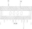
- FIG. 4 is a schematic structural diagram of a display panel provided by an embodiment of the application.
- FIG. 5 is a schematic structural diagram of another display panel provided by an embodiment of the application.
- connection should be interpreted broadly unless otherwise clearly specified and limited.
- it can be a fixed connection or a detachable connection. Connected or integrally connected; it can be a mechanical connection or an electrical connection; it can be directly connected or indirectly connected through an intermediate medium, and it can be the internal communication between two components.
- connection should be interpreted broadly unless otherwise clearly specified and limited.
- it can be a fixed connection or a detachable connection. Connected or integrally connected; it can be a mechanical connection or an electrical connection; it can be directly connected or indirectly connected through an intermediate medium, and it can be the internal communication between two components.
- an embodiment of the present application provides a TFT array substrate 1, including a base substrate 2, an anti-reflection layer 3, and a gate insulating layer 4;
- the TFT array substrate 1 includes a light-transmitting area 5;
- the reflective layer 3 is arranged on the base substrate 2 in the light-transmitting area 5, and the gate insulating layer 4 is arranged on the anti-reflective layer 3; among them, the light refraction of the base substrate 2, the anti-reflective layer 3 and the gate insulating layer 4 The rate increases sequentially.
- the TFT array substrate 1 further includes a passivation layer 10 and a pixel electrode layer 11 arranged on the gate insulating layer 4 in the light-transmitting area 5; the backlight is from the base substrate 2 side of the TFT array substrate 1 to the pixel electrode layer The direction of 11 provides the light source.
- the anti-reflection layer 3 is provided between the base substrate 2 and the gate insulating layer 4 in the light-transmitting area 5 of the TFT array substrate 1, and the base substrate 2, the anti-reflection layer 3 and the gate insulating layer
- the light refractive index of 4 gradually increases, so that the backlight enters the light-dense medium in the light-transmitting area 5 of the TFT array substrate 1 to form a half-wave loss, which reduces the reflected light energy and avoids the contrast of the light refractive index of the backlight.
- the high reflection phenomenon of the contact interface between the large base substrate 2 and the gate insulating layer 4 reduces the reflectivity of the contact interface of the backlight in the light-transmitting area 5, thereby increasing the backlight in the light-transmitting area 5 of the TFT array substrate 1.
- the penetration rate The high reflection phenomenon of the contact interface between the large base substrate 2 and the gate insulating layer 4 reduces the reflectivity of the contact interface of the backlight in the light-transmitting area 5, thereby increasing the backlight in the light-transmitting area 5 of the TFT array substrate 1.
- the TFT array substrate 1 further includes a non-transmissive area 6; the anti-reflection layer 3 is also disposed on the base substrate 2 in the non-transmissive area 6; and the anti-reflection layer 3 is located in the non-transmissive area 6.
- a gate layer 7 is provided; the gate insulating layer 4 is also provided on the gate layer 7.
- the TFT array substrate 1 further includes a semiconductor layer 8 (including the a-Si semiconductor active layer 19 and the n+a-Si ohmic contact layer 20) arranged on the gate insulating layer 4 in the non-transmissive area 6 in order, source and drain The electrode layer 9, the passivation layer 10 and the pixel electrode layer 11.
- a semiconductor layer 8 including the a-Si semiconductor active layer 19 and the n+a-Si ohmic contact layer 20 arranged on the gate insulating layer 4 in the non-transmissive area 6 in order, source and drain
- the electrode layer 9 the passivation layer 10 and the pixel electrode layer 11.
- an anti-reflection layer 3 is also provided between the base substrate 2 and the gate layer 7 in the non-transmissive area 6 of the TFT array substrate 1, increasing the gap between the base substrate 2 and the gate layer 7.
- the number of interfaces is shown in Figure 2.
- the backlight source that cannot pass through the gate layer 7 passes through the contact interface between the base substrate 2 and the anti-reflection layer 3 and the contact interface between the anti-reflection layer 3 and the gate layer 7 many times. Part of the light source passes through the light-transmitting area 5 of the TFT array substrate 1 after reflection, which further improves the transmittance of the backlight in the light-transmitting area 5 of the TFT array substrate 1.
- the non-transmissive area 6 includes a first non-transmissive area 22 and a second non-transmissive area 23;
- the gate layer 7 includes a gate 14 and a first metal electrode 15 (scanning line) formed by the same process.
- the source and drain electrode layer 9 includes the source electrode 16 and the drain electrode 17 and the second metal electrode 18 (data line) formed in the same process;
- the TFT array substrate 1 includes the base substrate 2 in the first non-transmissive area 22 and is sequentially arranged on the liner
- the TFT array substrate 1 is in the second non-transparent
- the light zone 23 includes a base substrate 2 and an anti-reflection layer 3, a first metal electrode 15, a gate insulating layer 4, a second metal electrode 18, a passivation layer 10, and a pixel electrode layer 11 sequentially disposed
- the anti-reflection layer 3 is provided between the base substrate 2 and the gate 14, and in the second non-transmissive area 23, the anti-reflection layer 3 is provided on the base substrate 2 and the first metal electrode 15, the number of contact interfaces between the first non-transmissive area 22 and the second non-transmissive area 23 is increased, so that the backlight source that cannot pass through the gate 14 and the first metal electrode 15 is on the base substrate 2
- the contact interface with the anti-reflective layer 3, the contact interface between the anti-reflective layer 3 and the gate 14, and the contact interface between the anti-reflective layer 3 and the first metal electrode 15 undergo multiple reflections. After multiple reflections, part of the light source passes from the light-transmitting area of the TFT array substrate 1. 5 through, further improving the transmittance of the backlight in the light-transmitting area 5 of the TFT array substrate 1.
- the anti-reflection layer 3 includes multiple film layers (not shown) sequentially superimposed on the base substrate 2, and the light refractive index of each film layer is greater than that of the base substrate 2, and It is smaller than the optical refractive index of the gate insulating layer 4; in the direction toward the gate insulating layer 4, the optical refractive index of the multilayer film layer increases layer by layer.
- the anti-reflection layer 3 can also be composed of a single film layer.
- each film layer includes any one of silicon oxynitride (optical refractive index range of 1.46 to 1.92), aluminum oxide (optical refractive index range of 1.59 to 1.77), and resin compounds.
- silicon oxynitride optical refractive index range of 1.46 to 1.92
- aluminum oxide optical refractive index range of 1.59 to 1.77
- resin compounds resin compounds.
- the material of the anti-reflection layer 3 in the embodiment of the present application is not limited to this.
- the anti-reflection layer 3 composed of a multilayer film with increasing light refractive index layer by layer enhances the light transmittance.
- the anti-reflection layer 3 is arranged on the base substrate 2 (for example, a glass substrate with a light refractive index of about 1.52) and a gate insulating layer 4 with a relatively large light refractive index (for example, a gate insulating layer 4 formed of silicon nitride, with a light refractive index of about 2.0), so that the substrate From the substrate 2 to the gate insulating layer 4, the light refractive index increases layer by layer, so that the backlight enters the optically dense medium from the light-thin medium in the light-transmitting area 5 of the TFT array substrate 1 to form a half-wave loss, which reduces the reflected light energy and reduces
- the reflectivity of each contact interface of the backlight in the light-transmitting area 5 improves the transmittance of the backlight in the light-transmitting area 5 of the TFT array substrate 1.
- the light refractive index of the anti-reflection layer 3 is Among them, n is the optical refractive index of the anti-reflection layer 3, n1 is the optical refractive index of the base substrate 2 and n2 is the optical refractive index of the gate insulating layer 4.
- the light refractive index of the anti-reflection layer 3 can be determined by the light refractive index of the base substrate 2 and the gate insulating layer 4, and the material of the anti-reflection layer 3 can be selected according to the calculated light refractive index.
- the thickness of the anti-reflection layer 3 is Where, e is the thickness of the anti-reflection layer 3, k is a natural number, and ⁇ is a green light wavelength with a wavelength of 550 nanometers. In this embodiment, the thickness of the anti-reflection layer 3 is determined by the light refractive index of the anti-reflection layer 3 and the wavelength of light.
- the gate insulating layer 4 includes a first gate insulating layer 12 and a second gate insulating layer 13 sequentially disposed on the gate layer 7.
- the first gate insulating layer 12 It is different from the material of the second gate insulating layer 13.
- the material of the first gate insulating layer 12 and the second gate insulating layer 13 includes silicon nitride or silicon oxide.
- the material of the first gate insulating layer 12 and the second gate insulating layer 13 includes silicon nitride or silicon oxide, where silicon nitride can effectively isolate oxygen and prevent the gate layer 7 from being oxidized and deposited to form The silicon oxide can effectively isolate hydrogen and prevent the semiconductor layer 8 from being reduced. Therefore, the gate insulating layer 4 of the double-layer structure can protect both the gate layer 7 and the semiconductor layer 8.
- the aforementioned TFT array substrate 1 is prepared through the following steps:
- the anti-reflection layer 3 is formed on the base substrate 2 by magnetron sputtering or vapor deposition process;
- a metal layer film including molybdenum, aluminum, copper, etc.
- a magnetron sputtering process depositing a metal layer film (including molybdenum, aluminum, copper, etc.) on the anti-reflection layer 3 through a magnetron sputtering process, and forming a pattern of the gate layer 7 through a yellow light process and a wet etching process;
- the gate insulating layer 4 and the semiconductor layer 8 are sequentially formed on the gate layer 7 through a vapor deposition process; and through a yellow light process and a dry method The etching process forms a pattern of the a-Si semiconductor layer 8;
- a metal layer film (including molybdenum, aluminum, copper, etc.) is deposited on the base substrate 2 after the semiconductor layer 8 is formed by a magnetron sputtering process, and a source and drain electrode layer is formed by a yellow light process and a wet etching process 9 pattern, and then through a dry etching process, the ohmic contact layer 20 at the channel of the source and drain electrode layer 9 is etched away to obtain a TFT channel;
- a non-metallic film (including silicon nitride or silicon oxide, etc.) is deposited on the base substrate 2 after the source and drain electrode layer 9 is formed by a vapor deposition process, and passivation is formed by a yellow light process and a dry etching process Layer 10 via pattern;
- a layer of ITO (Indium-Tin Oxide, indium tin oxide) film is formed on the base substrate 2 after the passivation layer 10 is formed by a magnetron sputtering deposition process, and a pixel electrode is formed by a yellow light process and a wet etching process Layer 11 pattern.
- ITO Indium-Tin Oxide, indium tin oxide
- the TFT array substrate 1 prepared by the above method is provided with an anti-reflection layer 3, and specifically, the anti-reflection layer 3 is provided between the base substrate 2 and the gate insulating layer 4, so that the base substrate 2, the anti-reflection layer
- the light refractive index of the layer 3 and the gate insulating layer 4 gradually increases, so that the backlight enters the light-dense medium from the light-thin medium in the light-transmitting area 5 of the TFT array substrate 1 to form a half-wave loss, which reduces the reflected light energy and avoids
- the high reflection phenomenon of the backlight at the contact interface between the base substrate 2 and the gate insulating layer 4 with a large difference in light refractive index reduces the reflectivity of each contact interface of the backlight in the light-transmitting zone 5, thereby improving the backlight
- an embodiment of the present application also provides a display panel 21, which includes the above TFT array substrate 1, a color filter substrate 24 arranged in a box with the TFT array substrate 1, and a color filter substrate 24 arranged on the TFT array substrate 1 and the color filter substrate.
- the liquid crystal layer between 24 and the backlight provided on the side of the TFT array substrate 1 away from the color filter substrate 24.
- the backlight provides a light source from the side of the TFT array substrate 1 to the side of the color filter substrate 24, and an anti-reflection is provided between the base substrate 2 and the gate insulating layer 4 in the light-transmitting area 5 of the TFT array substrate 1.
- the anti-reflection layer 3 and the gate insulating layer 4 gradually increase, so that the backlight in the light-transmitting area 5 of the TFT array substrate 1 enters the optically dense medium to form a semi
- the wave loss reduces the reflected light energy, avoids the high reflection phenomenon of the backlight at the contact interface between the substrate 2 and the gate insulating layer 4 with a large difference in optical refractive index, and reduces the contact interface of the backlight in the light-transmitting area 5.
- the anti-reflection layer 3 is also provided, which increases the number of interfaces between the base substrate 2 and the gate layer 7, so that the backlight source that cannot pass through the gate layer 7 is at the contact interface between the base substrate 2 and the anti-reflection layer 3. And after multiple reflections at the contact interface between the anti-reflection layer 3 and the gate layer 7, part of the light source passes through the light-transmitting area 5 of the TFT array substrate 1, further improving the transmittance of the backlight on the TFT array substrate 1.
- an embodiment of the present application also provides a display panel 21, which includes the above TFT array substrate 1 and a color resist layer 25 provided on the TFT array substrate 1.
- the display panel 21 includes a display panel with a color filter on Array (COA) disposed on the TFT array substrate 1 or a spacer (Post Spacer, PS) disposed on the TFT array substrate 1 ( PS on Array (POA) display panel, in which the color resistive layer of the POA display panel is also arranged on the TFT array substrate.
- COA color filter on Array
- PS PS on Array
- the anti-reflection layer 3 of the TFT array substrate 1 is provided between the base substrate 2 and the gate insulating layer 4.
- the manufacturing process of the anti-reflection layer 3 and the color resist layer 25 and spacers are not mutually exclusive. Therefore, the aforementioned TFT array substrate 1 with high light transmittance can be applied to different types of display panels, including COA display panels and POA display panels.
Landscapes
- Physics & Mathematics (AREA)
- Nonlinear Science (AREA)
- General Physics & Mathematics (AREA)
- Optics & Photonics (AREA)
- Mathematical Physics (AREA)
- Chemical & Material Sciences (AREA)
- Crystallography & Structural Chemistry (AREA)
- Engineering & Computer Science (AREA)
- Microelectronics & Electronic Packaging (AREA)
- Liquid Crystal (AREA)
- Thin Film Transistor (AREA)
Abstract
一种TFT阵列基板(1)及显示面板,其中,TFT阵列基板(1)包括衬底基板(2)、减反射层(3)和栅极绝缘层(4);所述TFT阵列基板(1)包括透光区(5);所述减反射层(3)设置在位于所述透光区(5)的衬底基板(2)上,所述栅极绝缘层(4)设置在所述减反射层(3)上;所述衬底基板(1)、所述减反射层(3)和所述栅极绝缘层(4)的光折射率依次增大。
Description
本申请涉及显示面板技术领域,尤其涉及一种TFT阵列基板及显示面板。
这里的陈述仅提供与本申请有关的背景信息,而不必然地构成现有技术。
现有市场上的液晶显示装置大部分为背光型液晶显示装置,其包括液晶显示面板及背光模组(backlight module),液晶显示面板本身不会发光,必须通过背光模块提供光源。液晶显示面板一般包括薄膜晶体管(Thin Film Transistor,TFT)阵列基板、彩膜(Color Filter,CF)基板、以及配置于两基板间的液晶层(Liquid Crystal Layer),其工作原理是通过在两片基板上施加驱动电压来控制液晶层的液晶分子旋转,将背光模组的光线折射出来产生画面。
通常背光源从TFT阵列基板侧入射,从CF基板侧出来,背光源入射到TFT阵列基板的衬底基板与栅极绝缘层接触界面时,在接触界面处有较高的光反射现象,降低了背光源的穿透率。并且,随着大尺寸和高分辨率的技术发展趋势,液晶显示面板的像素密度密度越来越大,对于高像素密度的显示面板,像素设计较小,开口率较低,衬底基板与栅极绝缘层接触界面的入射光高反射造成背光源损失更大,使得背光源在TFT阵列基板上的穿透率更低。
本申请提供一种TFT阵列基板及显示面板,通过在TFT阵列基板的衬底基板和栅极绝缘层之间以及衬底基板和栅极层之间设置光折射率介于衬底基板和栅极绝缘层的光折射率之间的减反射层,解决了背光源在TFT阵列基板上的穿透率低的技术问题。
为解决上述问题,本申请提供的技术方案如下:
本申请实施例提供了一种TFT阵列基板,包括衬底基板、减反射层和栅极绝缘层;所述TFT阵列基板包括透光区;所述减反射层设置在位于所述透光区的衬底基板上,所述栅极绝缘层设置在所述减反射层上;
其中,所述衬底基板、所述减反射层和所述栅极绝缘层的光折射率依次增大。
在本申请实施例提供的TFT阵列基板中,所述TFT阵列基板还包括非透光区;所述减反射层还设置在位于所述非透光区的衬底基板上;位于所述非透光区的减 反射层上设有栅极层;所述栅极绝缘层还设置在所述栅极层上。
在本申请实施例提供的TFT阵列基板中,所述TFT阵列基板还包括依次设置在所述栅极绝缘层上的半导体层、源漏电极层、钝化层及像素电极层。
在本申请实施例提供的TFT阵列基板中,所述栅极绝缘层包括依次设置在所述栅极层上的第一栅极绝缘层和第二栅极绝缘层,所述第一栅极绝缘层和第二栅极绝缘层的材料不同。
在本申请实施例提供的TFT阵列基板中,所述第一栅极绝缘层和所述第二栅极绝缘层的材料包括氮化硅或氧化硅。
在本申请实施例提供的TFT阵列基板中,所述减反射层包括依次叠加在所述衬底基板上的多层膜层,每层膜层的光折射率大于所述衬底基板的光折射率,且小于所述栅极绝缘层的光折射率;在朝向所述栅极绝缘层的方向上,所述多层膜层的光折射率逐层增大。
在本申请实施例提供的TFT阵列基板中,每层膜层的材料包括氮氧化硅、三氧化二铝和树脂类化合物中的任意一种。
在本申请实施例提供的TFT阵列基板中,所述减反射层的光折射率为
 其中,n为所述减反射层的光折射率,n1为所述衬底基板的光折射率,n2为所述栅极绝缘层的光折射率。
在本申请实施例提供的TFT阵列基板中,所述减反射层的厚度为
 其中,e为所述减反射层的厚度,k为自然数,λ为波长为550纳米的绿光波长。
在本申请实施例提供的TFT阵列基板中,所述非透光区包括第一非透光区和第二非透光区;所述栅极层包括栅极和第一金属电极;所述源漏电极层包括源极、漏极和第二金属电极;位于所述第一非透光区的TFT阵列基板包括依次设置在所述衬底基板上的所述减反射层、栅极、栅极绝缘层、半导体层、源极、漏极、钝化层及像素电极层;位于所述第二非透光区的TFT阵列基板包括依次设置在所述衬底基板上的所述减反射层、第一金属电极、栅极绝缘层、第二金属电极、钝化层及像素电极层。
在本申请实施例提供的TFT阵列基板中,所述减反射层的制作工艺包括磁控溅射工艺或气相沉积工艺。
本申请实施例还提供了一种显示面板,包括以上所述的TFT阵列基板以及与所述TFT阵列基板对盒设置的彩膜基板。
本申请实施例还提供了一种显示面板,包括以上所述的TFT阵列基板以及 彩色色阻层,所述彩色色阻层设置在所述TFT阵列基板上。
本申请的有益效果为:本申请通过在位于TFT阵列基板的透光区的衬底基板和栅极绝缘层之间设置减反射层,且衬底基板、减反射层和栅极绝缘层的光折射率逐渐增大,使得背光源在TFT阵列基板的透光区从光疏介质进入光密介质形成半波损失减少了反射光能量,避免了背光源在光折射率相差较大的衬底基板和栅极绝缘层的接触界面的高反射现象,降低了背光源在透光区各接触界面的反射率,从而提高了背光源在TFT阵列基板的透光区的穿透率;另外,在位于TFT阵列基板的非透光区的衬底基板和栅极层之间也设置了减反射层,增加了衬底基板和栅极层之间的接触界面数量,使原本无法透过栅极层的背光源在衬底基板与减反射层的接触界面以及减反射层与栅极层的接触界面经过多次反射后部分光源从TFT阵列基板的透光区透过,进一步提高了背光源在TFT阵列基板的透光区的穿透率。
为了更清楚地说明实施例或现有技术中的技术方案,下面将对实施例或现有技术描述中所需要使用的附图作简单介绍,显而易见地,下面描述中的附图仅仅是申请的一些实施例,对于本领域普通技术人员来讲,在不付出创造性劳动的前提下,还可以根据这些附图获得其他的附图。
图1为本申请实施例提供的一种TFT阵列基板的结构示意图;
图2为本申请实施例提供的一种TFT阵列基板的局部结构示意图;
图3为本申请实施例提供的另一种TFT阵列基板的局部结构示意图;
图4为本申请实施例提供的一种显示面板的结构示意图;
图5为本申请实施例提供的另一种显示面板的结构示意图。
这里所公开的具体结构和功能细节仅仅是代表性的,并且是用来描述本申请的示例性实施例的目的。但是本申请可以通过许多替换形式来具体实现,并且不应当被解释成仅仅受限于这里所阐述的实施例。
在本申请的描述中,需要理解的是,术语“中心”、“横向”、“上”、“下”、“左”、“右”、“竖直”、“水平”、“顶”、“底”、“内”、“外”等指示的方位或位置关系为基于附图所示的方位或位置关系,仅是为了便于描述本申请和简化描述,而不是指示或暗示所指的装置或元件必须具有特定的方位、以特 定的方位构造和操作,因此不能理解为对本申请的限制。此外,术语“第一”、“第二”仅用来描述目的,而不能理解为指示或暗示相对重要性或者隐含指明所指示的技术特征的数量。由此,限定有“第一”、“第二”的特征可以明示或者隐含地包括一个或者更多个该特征。在本申请的描述中,除非另有说明,“多个”的含义是两个或两个以上。另外,术语“包括”及其任何变形,意图在于覆盖不排他的包含。
在本申请的描述中,需要说明的是,除非另有明确的规定和限定,术语“安装”、“相连”、“连接”应做广义理解,例如,可以是固定连接,也可以是可拆卸连接,或一体地连接;可以是机械连接,也可以是电连接;可以是直接相连,也可以通过中间媒介间接相连,可以是两个元件内部的连通。对于本领域的普通技术人员而言,可以具体情况理解上述术语在本申请中的具体含义。
这里所使用的术语仅仅是为了描述具体实施例而不意图限制示例性实施例。除非上下文明确地另有所指,否则这里所使用的单数形式“一个”、“一项”还意图包括复数。还应当理解的是,这里所使用的术语“包括”和/或“包含”规定所陈述的特征、整数、步骤、操作、单元和/或组件的存在,而不排除存在或添加一个或更多其他特征、整数、步骤、操作、单元、组件和/或其组合。
下面结合附图和实施例对本申请作进一步说明。
如图1和图2所示,本申请实施例提供了一种TFT阵列基板1,包括衬底基板2、减反射层3和栅极绝缘层4;TFT阵列基板1包括透光区5;减反射层3设置在位于透光区5的衬底基板2上,栅极绝缘层4设置在减反射层3上;其中,衬底基板2、减反射层3和栅极绝缘层4的光折射率依次增大。
具体的,TFT阵列基板1在透光区5还包括依次设置栅极绝缘层4上的钝化层10和像素电极层11;背光源从TFT阵列基板1的衬底基板2侧向像素电极层11的方向提供光源。
本实施例中,在位于TFT阵列基板1的透光区5的衬底基板2和栅极绝缘层4之间设置减反射层3,且衬底基板2、减反射层3和栅极绝缘层4的光折射率逐渐增大,使得背光源在TFT阵列基板1的透光区5从光疏介质进入光密介质形成半波损失减少了反射光能量,避免了背光源在光折射率相差较大的衬底基板2和栅极绝缘层4的接触界面的高反射现象,降低了背光源在透光区5接触界面的反射率,从而提高了背光源在TFT阵列基板1的透光区5的穿透率。
在一实施例中,TFT阵列基板1还包括非透光区6;减反射层3还设置在位于非透光区6的衬底基板2上;位于非透光区6的减反射层3上设有栅极层7;栅极绝缘层4还设置在栅极层7上。
具体的,TFT阵列基板1在非透光区6还包括依次设置栅极绝缘层4上的半 导体层8(包括a-Si半导体活性层19和n+a-Si欧姆接触层20)、源漏电极层9、钝化层10及像素电极层11。
本实施例中,在位于TFT阵列基板1的非透光区6的衬底基板2和栅极层7之间也设置了减反射层3,增加了衬底基板2和栅极层7之间的界面数量,如图2所示,原本无法透过栅极层7的背光源在衬底基板2与减反射层3的接触界面以及减反射层3与栅极层7的接触界面经过多次反射后部分光源从TFT阵列基板1的透光区5透过,进一步提高了背光源在TFT阵列基板1的透光区5的穿透率。
在一实施例中,非透光区6包括第一非透光区22和第二非透光区23;栅极层7包括同制程形成的栅极14和第一金属电极15(扫描线);源漏电极层9包括同制程形成的源极16漏极17和第二金属电极18(数据线);TFT阵列基板1在第一非透光区22包括衬底基板2以及依次设置在衬底基板2上的减反射层3、栅极14、栅极绝缘层4、半导体层8、源极16漏极17、钝化层10及像素电极层11;TFT阵列基板1在第二非透光区23包括衬底基板2以及依次设置在衬底基板2上的减反射层3、第一金属电极15、栅极绝缘层4、第二金属电极18、钝化层10及像素电极层11。在第一非透光区22,减反射层3设在衬底基板2和栅极14之间,在第二非透光区23,减反射层3设在衬底基板2和第一金属电极15之间,分别增加了第一非透光区22和第二非透光区23的接触界面的数量,使原本无法透过栅极14和第一金属电极15的背光源在衬底基板2与减反射层3的接触界面、减反射层3与栅极14的接触界面以及减反射层3与第一金属电极15的接触界面经过多次反射后部分光源从TFT阵列基板1的透光区5透过,进一步提高了背光源在TFT阵列基板1的透光区5的穿透率。
在一实施例中,减反射层3包括依次叠加在衬底基板2上的多层膜层(未提供图示),每层膜层的光折射率大于衬底基板2的光折射率,且小于栅极绝缘层4的光折射率;在朝向栅极绝缘层4的方向上,多层膜层的光折射率逐层增大。当然,减反射层3还可以由单层膜层组成。
具体的,每层膜层的材料包括氮氧化硅(光折射率范围为1.46~1.92)、三氧化二铝(光折射率范围为1.59~1.77)和树脂类化合物中的任意一种,当然,本申请实施例中的减反射层3的材料不限于此。
本实施例中,由光折射率逐层增大的多层膜层组成的减反射层3,增强了光的透射性,该减反射层3设置在光折射率较小的衬底基板2(例如玻璃基板,光折射率约为1.52)和光折射率较大的栅极绝缘层4(例如由氮化硅形成的栅极绝缘层4,光折射率约为2.0)之间,使得从衬底基板2至栅极绝缘层4,光折射率逐层增大,使得背光源在TFT阵列基板1的透光区5从光疏介质进入光密介质形成半波损失减少了反射光能量,降低了背光源在透光区5各接触界面的反射 率,从而提高了背光源在TFT阵列基板1的透光区5的穿透率。
在一实施例中,减反射层3的光折射率为
 其中,n为减反射层3的光折射率,n1为衬底基板2的光折射率,n2为栅极绝缘层4的光折射率。
本实施例中,减反射层3的光折射率可以由衬底基板2和栅极绝缘层4的光折射率决定,并可以依据计算得到的光折射率来选择减反射层3的材料。
在一实施例中,减反射层3的厚度为
 其中,e为减反射层3的厚度,k为自然数,λ为波长为550纳米的绿光波长。本实施例中,减反射层3的厚度由减反射层3的光折射率和光的波长决定。
在一实施例中,如图3所示,栅极绝缘层4包括依次设置在栅极层7上的第一栅极绝缘层12和第二栅极绝缘层13,第一栅极绝缘层12和第二栅极绝缘层13的材料不同。具体的,第一栅极绝缘层12和第二栅极绝缘层13的材料包括氮化硅或氧化硅。
本实施例中,第一栅极绝缘层12和第二栅极绝缘层13的材料包括氮化硅或氧化硅,其中氮化硅可有效隔离氧,防止栅极层7被氧化,而沉积形成的氧化硅可有效隔离氢,防止半导体层8被还原,因此,双层结构的栅极绝缘层4既可以保护栅极层7也可以保护半导体层8。
在一实施例中,上述TFT阵列基板1通过以下步骤制备得到:
提供衬底基板2;
通过磁控溅射或气相沉积工艺在衬底基板2上形成减反射层3;
通过磁控溅射工艺在减反射层3上沉积一层金属层薄膜(包括钼、铝或铜等),并通过黄光工艺及湿法刻蚀工艺形成栅极层7图案;
通过气相沉积工艺在栅极层7上依次形成栅极绝缘层4、半导体层8(包括a-Si半导体活性层19和n+a-Si欧姆接触层20);并通过黄光工艺及干法刻蚀工艺形成a-Si半导体层8图案;
通过磁控溅射工艺在半导体层8形成后的衬底基板2上沉积一层金属层薄膜(包括钼、铝或铜等),并通过黄光工艺及湿法刻蚀工艺形成源漏电极层9图案,再经过干法刻蚀工艺将源漏电极层9沟道处的欧姆接触层20刻蚀掉而得到TFT沟道;
通过气相沉积工艺在源漏电极层9形成后的衬底基板2上沉积一层非金属层薄膜(包括氮化硅或氧化硅等),并通过黄光工艺及干法刻蚀工艺形成钝化层10过孔图案;
通过磁控溅射沉积工艺在钝化层10形成后的衬底基板2上形成一层ITO(Indium-Tin Oxide,氧化铟锡)薄膜,并通过黄光工艺及湿法刻蚀工艺形成像 素电极层11图案。
本实施例中,通过以上方法制备得到的TFT阵列基板1设有减反射层3,具体减反射层3设置在衬底基板2和栅极绝缘层4之间,使得衬底基板2、减反射层3和栅极绝缘层4的光折射率逐渐增大,从而使得背光源在TFT阵列基板1的透光区5从光疏介质进入光密介质形成半波损失减少了反射光能量,避免了背光源在光折射率相差较大的衬底基板2和栅极绝缘层4的接触界面的高反射现象,降低了背光源在透光区5各接触界面的反射率,从而提高了背光源在TFT阵列基板1的透光区5的穿透率;另外,减反射层3还设置在衬底基板2和栅极层7之间,增加了衬底基板2和栅极层7之间的界面数量,使原本无法透过栅极层7的背光源在衬底基板2与减反射层3的接触界面以及减反射层3与栅极层7的接触界面经过多次反射后部分光源从TFT阵列基板1的透光区5透过,进一步提高了背光源在TFT阵列基板1上的穿透率。
如图4所示,本申请实施例还提供了一种显示面板21,包括以上TFT阵列基板1、与TFT阵列基板1对盒设置的彩膜基板24、设置在TFT阵列基板1和彩膜基板24之间的液晶层、以及设置在TFT阵列基板1远离彩膜基板24的一侧的背光源。
本实施例中,背光源从TFT阵列基板1侧向彩膜基板24侧提供光源,通过在位于TFT阵列基板1的透光区5的衬底基板2和栅极绝缘层4之间设置减反射层3,且衬底基板2、减反射层3和栅极绝缘层4的光折射率逐渐增大,使得背光源在TFT阵列基板1的透光区5从光疏介质进入光密介质形成半波损失减少了反射光能量,避免了背光源在光折射率相差较大的衬底基板2和栅极绝缘层4的接触界面的高反射现象,降低了背光源在透光区5各接触界面的反射率,从而提高了背光源在TFT阵列基板1的透光区5的穿透率;另外,在位于TFT阵列基板1的非透光区6的衬底基板2和栅极层7之间也设置了减反射层3,增加了衬底基板2和栅极层7之间的界面数量,使原本无法透过栅极层7的背光源在衬底基板2与减反射层3的接触界面以及减反射层3与栅极层7的接触界面经过多次反射后部分光源从TFT阵列基板1的透光区5透过,进一步提高了背光源在TFT阵列基板1上的穿透率。
如图5所示,本申请实施例还提供了一种显示面板21,包括以上TFT阵列基板1和设置在TFT阵列基板1上的彩色色阻层25。具体的,显示面板21包括将彩色色阻层25设置到TFT阵列基板1上(Color Filter on Array,COA)的显示面板或将隔垫物(Post Spacer,PS)设置在TFT阵列基板1上(PS on Array,POA)的显示面板,其中POA显示面板的彩色色阻层也设置在TFT阵列基板上。
本实施例中,TFT阵列基板1的减反射层3设置在衬底基板2与栅极绝缘层4之 间,减反射层3的制程与彩色色阻层25和隔垫物的制程相互都没有影响,因此,上述光穿透率高的TFT阵列基板1可以应用到不同类型的显示面板中,包括COA显示面板和POA显示面板。
综上所述,虽然本申请已以优选实施例揭露如上,但上述优选实施例并非用以限制本申请,本领域的普通技术人员,在不脱离本申请的精神和范围内,均可作各种更动与润饰,因此本申请的保护范围以权利要求界定的范围为准。
Claims (13)
- 一种TFT阵列基板,包括衬底基板、减反射层和栅极绝缘层;所述TFT阵列基板包括透光区;所述减反射层设置在位于所述透光区的衬底基板上,所述栅极绝缘层设置在所述减反射层上;其中,所述衬底基板、所述减反射层和所述栅极绝缘层的光折射率依次增大。
- 如权利要求1所述的TFT阵列基板,其中,所述TFT阵列基板还包括非透光区;所述减反射层还设置在位于所述非透光区的衬底基板上;位于所述非透光区的减反射层上设有栅极层;所述栅极绝缘层还设置在所述栅极层上。
- 如权利要求2所述的TFT阵列基板,其中,所述TFT阵列基板还包括依次设置在所述栅极绝缘层上的半导体层、源漏电极层、钝化层及像素电极层。
- 如权利要求2所述的TFT阵列基板,其中,所述栅极绝缘层包括依次设置在所述栅极层上的第一栅极绝缘层和第二栅极绝缘层,所述第一栅极绝缘层和第二栅极绝缘层的材料不同。
- 如权利要求4所述的TFT阵列基板,其中,所述第一栅极绝缘层和所述第二栅极绝缘层的材料包括氮化硅或氧化硅。
- 如权利要求1所述的TFT阵列基板,其中,所述减反射层包括依次叠加在所述衬底基板上的多层膜层,每层膜层的光折射率大于所述衬底基板的光折射率,且小于所述栅极绝缘层的光折射率;在朝向所述栅极绝缘层的方向上,所述多层膜层的光折射率逐层增大。
- 如权利要求6所述的TFT阵列基板,其中,每层膜层的材料包括氮氧化硅、三氧化二铝和树脂类化合物中的任意一种。
- 如权利要求1所述的TFT阵列基板,其中,所述减反射层的光折射率为其中,n为所述减反射层的光折射率,n1为所述衬底基板的光折射率,n2为所述栅极绝缘层的光折射率。

- 如权利要求8所述的TFT阵列基板,其中,所述减反射层的厚度为其中,e为所述减反射层的厚度,k为自然数,λ为波长为550纳米的绿光波长。

- 如权利要求3所述的TFT阵列基板,其中,所述非透光区包括第一非透光区和第二非透光区;所述栅极层包括栅极和第一金属电极;所述源漏电极层包括源极、漏极和第二金属电极;位于所述第一非透光区的TFT阵列基板包括依次设置在所述衬底基板上的所述减反射层、栅极、栅极绝缘层、半导体层、源极、漏极、钝化层及像素电极层;位于所述第二非透光区的TFT阵列基板包括依次设置在所述衬底基板上的所述减反射层、第一金属电极、栅极绝缘层、第二金属电 极、钝化层及像素电极层。
- 如权利要求1所述的TFT阵列基板,其中,所述减反射层的制作工艺包括磁控溅射工艺或气相沉积工艺。
- 一种显示面板,包括如权利要求1所述的TFT阵列基板以及与所述TFT阵列基板对盒设置的彩膜基板。
- 一种显示面板,包括如权利要求1所述的TFT阵列基板以及彩色色阻层,所述彩色色阻层设置在所述TFT阵列基板上。
Priority Applications (1)
| Application Number | Priority Date | Filing Date | Title |
|---|---|---|---|
| US16/607,191 US11251202B2 (en) | 2019-05-15 | 2019-05-28 | Thin film transistor (TFT) array substrate and display panel |
Applications Claiming Priority (2)
| Application Number | Priority Date | Filing Date | Title |
|---|---|---|---|
| CN201910402429.6A CN110082977B (zh) | 2019-05-15 | 2019-05-15 | 一种tft阵列基板及显示面板 |
| CN201910402429.6 | 2019-05-15 |
Publications (1)
| Publication Number | Publication Date |
|---|---|
| WO2020228058A1 true WO2020228058A1 (zh) | 2020-11-19 |
Family
ID=67420176
Family Applications (1)
| Application Number | Title | Priority Date | Filing Date |
|---|---|---|---|
| PCT/CN2019/088692 Ceased WO2020228058A1 (zh) | 2019-05-15 | 2019-05-28 | Tft阵列基板及显示面板 |
Country Status (3)
| Country | Link |
|---|---|
| US (1) | US11251202B2 (zh) |
| CN (1) | CN110082977B (zh) |
| WO (1) | WO2020228058A1 (zh) |
Families Citing this family (11)
| Publication number | Priority date | Publication date | Assignee | Title |
|---|---|---|---|---|
| CN110806665B (zh) | 2019-10-08 | 2021-09-24 | 武汉华星光电半导体显示技术有限公司 | 阵列基板及显示面板 |
| CN111063699B (zh) * | 2019-12-19 | 2022-08-26 | 京东方科技集团股份有限公司 | 阵列基板及其制备方法、显示装置 |
| CN113519061B (zh) * | 2020-02-10 | 2024-04-16 | 京东方科技集团股份有限公司 | 阵列基板及其制备方法、显示装置 |
| US11112634B1 (en) | 2020-04-07 | 2021-09-07 | Tcl China Star Optoelectronics Technology Co., Ltd. | Substrate and display device |
| CN111323960A (zh) * | 2020-04-07 | 2020-06-23 | Tcl华星光电技术有限公司 | 透光基板及显示装置 |
| CN111487826A (zh) * | 2020-05-12 | 2020-08-04 | Tcl华星光电技术有限公司 | 显示面板及其制作方法、显示终端 |
| CN112180629A (zh) * | 2020-10-16 | 2021-01-05 | Tcl华星光电技术有限公司 | 一种阵列基板及显示面板 |
| CN113126376A (zh) * | 2021-04-19 | 2021-07-16 | 合肥京东方显示技术有限公司 | 阵列基板及其制备方法、显示面板及显示装置 |
| CN114664867B (zh) * | 2022-03-11 | 2024-05-17 | 京东方科技集团股份有限公司 | 阵列基板、液晶显示面板和显示装置 |
| CN114924436B (zh) * | 2022-05-17 | 2023-12-12 | 武汉华星光电技术有限公司 | 阵列基板及液晶显示面板 |
| CN115207052B (zh) * | 2022-06-29 | 2024-07-05 | 上海天马微电子有限公司 | 显示面板及其制作方法、显示装置 |
Citations (5)
| Publication number | Priority date | Publication date | Assignee | Title |
|---|---|---|---|---|
| CN107085337A (zh) * | 2017-06-14 | 2017-08-22 | 厦门天马微电子有限公司 | 阵列基板、显示面板和显示装置 |
| CN107845647A (zh) * | 2017-10-31 | 2018-03-27 | 武汉华星光电技术有限公司 | 薄膜晶体管阵列基板及其制备方法、显示装置 |
| CN108336144A (zh) * | 2018-01-22 | 2018-07-27 | 惠州市华星光电技术有限公司 | 一种用于显示面板中的薄膜晶体管及显示面板 |
| US20190101788A1 (en) * | 2017-09-29 | 2019-04-04 | Boe Technology Group Co., Ltd. | Display panel and display apparatus |
| CN109696759A (zh) * | 2018-12-29 | 2019-04-30 | 武汉华星光电技术有限公司 | 高穿透性液晶显示面板制造方法及其显示面板 |
Family Cites Families (16)
| Publication number | Priority date | Publication date | Assignee | Title |
|---|---|---|---|---|
| JP2013037048A (ja) * | 2011-08-04 | 2013-02-21 | Japan Display East Co Ltd | 液晶表示装置 |
| CN103033977B (zh) * | 2012-12-14 | 2015-08-12 | 京东方科技集团股份有限公司 | 液晶显示装置 |
| JP2015060780A (ja) * | 2013-09-20 | 2015-03-30 | 株式会社東芝 | 表示装置の製造方法及び製造システム |
| KR102514716B1 (ko) * | 2015-10-05 | 2023-03-28 | 삼성디스플레이 주식회사 | 박막 트랜지스터 기판, 이를 포함하는 표시 장치, 및 박막 트랜지스터 기판의 제조 방법 |
| KR102435156B1 (ko) * | 2015-10-13 | 2022-08-24 | 삼성디스플레이 주식회사 | 투명 표시 기판 및 투명 표시 장치 |
| CN105304648A (zh) * | 2015-10-23 | 2016-02-03 | 京东方科技集团股份有限公司 | 一种阵列基板及其制作方法、显示装置 |
| CN205319159U (zh) * | 2016-01-21 | 2016-06-15 | 京东方科技集团股份有限公司 | 显示基板、显示面板以及显示装置 |
| JP2017224416A (ja) * | 2016-06-13 | 2017-12-21 | 株式会社ジャパンディスプレイ | 表示装置 |
| CN106057830A (zh) * | 2016-08-19 | 2016-10-26 | 京东方科技集团股份有限公司 | 一种阵列基板、显示面板及阵列基板制备方法 |
| CN106526949B (zh) * | 2016-11-15 | 2019-08-27 | 京东方科技集团股份有限公司 | 显示基板及其制造方法 |
| CN107045221A (zh) | 2016-12-28 | 2017-08-15 | 深圳市华星光电技术有限公司 | 液晶显示面板和液晶显示器 |
| KR102418493B1 (ko) * | 2017-10-24 | 2022-07-06 | 엘지디스플레이 주식회사 | 이차원 반도체를 포함하는 박막 트랜지스터 및 이를 포함하는 표시장치 |
| CN108508648B (zh) * | 2018-04-04 | 2020-01-17 | 深圳市华星光电技术有限公司 | 液晶面板及其制作方法 |
| CN109116615A (zh) * | 2018-08-20 | 2019-01-01 | 深圳市华星光电技术有限公司 | 彩膜基板及液晶面板 |
| CN109103205B (zh) * | 2018-08-21 | 2020-12-04 | 深圳市华星光电技术有限公司 | 一种阵列基板及其制造方法 |
| CN109656054A (zh) * | 2019-01-28 | 2019-04-19 | 深圳市华星光电技术有限公司 | 彩膜基板的制造方法 |
-
2019
- 2019-05-15 CN CN201910402429.6A patent/CN110082977B/zh active Active
- 2019-05-28 US US16/607,191 patent/US11251202B2/en active Active
- 2019-05-28 WO PCT/CN2019/088692 patent/WO2020228058A1/zh not_active Ceased
Patent Citations (5)
| Publication number | Priority date | Publication date | Assignee | Title |
|---|---|---|---|---|
| CN107085337A (zh) * | 2017-06-14 | 2017-08-22 | 厦门天马微电子有限公司 | 阵列基板、显示面板和显示装置 |
| US20190101788A1 (en) * | 2017-09-29 | 2019-04-04 | Boe Technology Group Co., Ltd. | Display panel and display apparatus |
| CN107845647A (zh) * | 2017-10-31 | 2018-03-27 | 武汉华星光电技术有限公司 | 薄膜晶体管阵列基板及其制备方法、显示装置 |
| CN108336144A (zh) * | 2018-01-22 | 2018-07-27 | 惠州市华星光电技术有限公司 | 一种用于显示面板中的薄膜晶体管及显示面板 |
| CN109696759A (zh) * | 2018-12-29 | 2019-04-30 | 武汉华星光电技术有限公司 | 高穿透性液晶显示面板制造方法及其显示面板 |
Also Published As
| Publication number | Publication date |
|---|---|
| US20210335832A1 (en) | 2021-10-28 |
| CN110082977B (zh) | 2020-11-24 |
| CN110082977A (zh) | 2019-08-02 |
| US11251202B2 (en) | 2022-02-15 |
Similar Documents
| Publication | Publication Date | Title |
|---|---|---|
| CN110082977B (zh) | 一种tft阵列基板及显示面板 | |
| CN102902118B (zh) | 面内转换模式液晶显示器件及其制造方法 | |
| JP3908552B2 (ja) | 液晶表示装置及びその製造方法 | |
| CN101299106B (zh) | 滤色器基板及包含该滤色器基板的液晶显示面板 | |
| KR101494951B1 (ko) | 간섭형 필터층 부착 기판 및 그것을 사용한 표시 장치 | |
| CN102629054A (zh) | 一种tft阵列基板及其制造方法、显示器件 | |
| WO2021196362A1 (zh) | 低温多晶硅显示面板及其制作方法、液晶显示装置 | |
| WO2024040751A1 (zh) | 显示面板及其制备方法、显示装置 | |
| CN114924436B (zh) | 阵列基板及液晶显示面板 | |
| CN100543566C (zh) | 制造显示基板的方法 | |
| WO2019192039A1 (zh) | 液晶面板及其制作方法 | |
| US10847076B2 (en) | Wiring substrate, display device including the wiring substrate, and method of fabricating the wiring substrate | |
| US11513400B2 (en) | Pixel array substrate and display device | |
| CN100523967C (zh) | 透射反射型液晶显示器及其制造方法 | |
| US20170160588A1 (en) | Reflective tft array panel, method of fabricating the same and lcd | |
| CN100585477C (zh) | 用于液晶显示装置的阵列基板及液晶显示装置 | |
| CN102116956A (zh) | 半透射半反射式液晶显示面板及其制作方法 | |
| JP4019080B2 (ja) | 液晶表示装置の製造方法 | |
| TWI918211B (zh) | 顯示面板及其陣列基板 | |
| WO2017012174A1 (zh) | 一种平板显示器中的面板结构及制作方法 | |
| TWI333112B (en) | Liquid crystal driving electrode and liquid crystal display using the same | |
| US20260126691A1 (en) | Display panel and array substrate thereof | |
| US20210255381A1 (en) | Collimating backlight module, preparation method thereof and display device | |
| CN116165817B (zh) | 一种显示面板及显示装置 | |
| KR20110029921A (ko) | 반사투과형 액정표시장치 및 그 제조 방법 |
Legal Events
| Date | Code | Title | Description |
|---|---|---|---|
| 121 | Ep: the epo has been informed by wipo that ep was designated in this application |
Ref document number: 19928337 Country of ref document: EP Kind code of ref document: A1 |
|
| NENP | Non-entry into the national phase |
Ref country code: DE |
|
| 122 | Ep: pct application non-entry in european phase |
Ref document number: 19928337 Country of ref document: EP Kind code of ref document: A1 |