WO2020226078A1 - 導光素子および画像表示装置 - Google Patents
導光素子および画像表示装置 Download PDFInfo
- Publication number
- WO2020226078A1 WO2020226078A1 PCT/JP2020/017754 JP2020017754W WO2020226078A1 WO 2020226078 A1 WO2020226078 A1 WO 2020226078A1 JP 2020017754 W JP2020017754 W JP 2020017754W WO 2020226078 A1 WO2020226078 A1 WO 2020226078A1
- Authority
- WO
- WIPO (PCT)
- Prior art keywords
- diffraction element
- diffraction
- liquid crystal
- incident
- light
- Prior art date
- Legal status (The legal status is an assumption and is not a legal conclusion. Google has not performed a legal analysis and makes no representation as to the accuracy of the status listed.)
- Ceased
Links
Images






Classifications
-
- G—PHYSICS
- G02—OPTICS
- G02B—OPTICAL ELEMENTS, SYSTEMS OR APPARATUS
- G02B27/00—Optical systems or apparatus not provided for by any of the groups G02B1/00 - G02B26/00, G02B30/00
- G02B27/0018—Optical systems or apparatus not provided for by any of the groups G02B1/00 - G02B26/00, G02B30/00 with means for preventing ghost images
-
- G—PHYSICS
- G02—OPTICS
- G02B—OPTICAL ELEMENTS, SYSTEMS OR APPARATUS
- G02B27/00—Optical systems or apparatus not provided for by any of the groups G02B1/00 - G02B26/00, G02B30/00
- G02B27/01—Head-up displays
- G02B27/017—Head mounted
- G02B27/0172—Head mounted characterised by optical features
-
- G—PHYSICS
- G02—OPTICS
- G02B—OPTICAL ELEMENTS, SYSTEMS OR APPARATUS
- G02B27/00—Optical systems or apparatus not provided for by any of the groups G02B1/00 - G02B26/00, G02B30/00
- G02B27/42—Diffraction optics, i.e. systems including a diffractive element being designed for providing a diffractive effect
- G02B27/4205—Diffraction optics, i.e. systems including a diffractive element being designed for providing a diffractive effect having a diffractive optical element [DOE] contributing to image formation, e.g. whereby modulation transfer function MTF or optical aberrations are relevant
-
- G—PHYSICS
- G02—OPTICS
- G02B—OPTICAL ELEMENTS, SYSTEMS OR APPARATUS
- G02B27/00—Optical systems or apparatus not provided for by any of the groups G02B1/00 - G02B26/00, G02B30/00
- G02B27/42—Diffraction optics, i.e. systems including a diffractive element being designed for providing a diffractive effect
- G02B27/4272—Diffraction optics, i.e. systems including a diffractive element being designed for providing a diffractive effect having plural diffractive elements positioned sequentially along the optical path
-
- G—PHYSICS
- G02—OPTICS
- G02B—OPTICAL ELEMENTS, SYSTEMS OR APPARATUS
- G02B5/00—Optical elements other than lenses
- G02B5/30—Polarising elements
- G02B5/3016—Polarising elements involving passive liquid crystal elements
-
- G—PHYSICS
- G02—OPTICS
- G02B—OPTICAL ELEMENTS, SYSTEMS OR APPARATUS
- G02B27/00—Optical systems or apparatus not provided for by any of the groups G02B1/00 - G02B26/00, G02B30/00
- G02B27/01—Head-up displays
- G02B27/0101—Head-up displays characterised by optical features
- G02B2027/0112—Head-up displays characterised by optical features comprising device for genereting colour display
-
- G—PHYSICS
- G02—OPTICS
- G02B—OPTICAL ELEMENTS, SYSTEMS OR APPARATUS
- G02B27/00—Optical systems or apparatus not provided for by any of the groups G02B1/00 - G02B26/00, G02B30/00
- G02B27/01—Head-up displays
- G02B27/017—Head mounted
- G02B27/0172—Head mounted characterised by optical features
- G02B2027/0174—Head mounted characterised by optical features holographic
Definitions
- the present invention relates to a light guide element that propagates light and an image display device that uses this light guide element.
- AR glasses In recent years, AR (Augmented Reality) glasses have been put into practical use, which superimpose virtual images and various kinds of information on the scene actually viewed as described in Non-Patent Document 1. There is. AR glasses are also called smart glasses, head-mounted displays (HMD (Head Mounted Display)), AR glasses, and the like.
- HMD Head Mounted Display
- Non-Patent Document 1 As shown in Non-Patent Document 1, as an example, in the AR glass, the image displayed by the display (optical engine) is incident on one end of the light guide plate and propagated, and then emitted from the other end, whereby the user A virtual image is superimposed on the actual scene.
- a diffraction element is used to diffract (refract) the light (projected light) from the display and incident it on one end of the light guide plate.
- light is introduced into the light guide plate at an angle, and the light is totally reflected and propagated in the light guide plate.
- the light propagating through the light guide plate is also diffracted by the diffraction element at the other end of the light guide plate, and is emitted from the light guide plate to the observation position by the user.
- an image consisting of light having three color wavelengths of R (red), G (green), and B (blue) is irradiated from the display, and each light is diffracted into the light guide plate.
- a color image can be displayed by guiding the light and emitting it from the light guide plate by a diffractive element to an observation position by the user and superimposing and displaying an image of three-color light (see Patent Document 1). ..
- the period of the diffraction structure is different between the G diffraction element and the R diffraction element and the B diffraction element.
- the diffraction angle by the diffractive element depends on the period of the diffractive structure of the diffractive element and the wavelength of light. Therefore, the G light diffracted by the G diffracting element, the G light diffracted by the R diffracting element, and the G light diffracted by the B diffracting element are diffracted at different angles. Similarly, some of the R light and the B light are diffracted at different angles by a diffractive element other than the corresponding diffractive element. As a result, the multiple image is visually recognized.
- An object of the present invention is to solve such a problem of the prior art, and to provide a light guide element capable of suppressing the generation of multiple images and an image display device using this light guide element.
- the present invention has the following configuration. [1] It has a light guide plate and a first incident diffraction element, a second incident diffraction element, a first emission diffraction element, and a second emission diffraction element provided on the light guide plate.
- the first incident diffractometer and the second incident diffractometer diffract the incident light in different directions and cause the incident light to enter the light guide plate.
- the first exit diffraction element is one that diffracts the light by the first incident diffraction element and emits the light propagated in the light guide plate from the light guide plate.
- the second exit diffractometer is for emitting light that has been diffracted by the second incident diffractometer and propagated in the light guide plate from the light guide plate.
- the period of the diffraction structure of the first incident diffraction element and the period of the diffraction structure of the second incident diffraction element are different.
- the period of the diffraction structure of the first emission diffraction element and the period of the diffraction structure of the second emission diffraction element are different.
- the first emission diffraction element and the second emission diffraction element are arranged at overlapping positions in the surface direction of the main surface of the light guide plate.
- a light guide element in which the periodic direction of the diffraction structure of the first emission diffraction element and the periodic direction of the diffraction structure of the second emission diffraction element intersect. [2] Further, it has a first intermediate diffraction element and a second intermediate diffraction element provided on the light guide plate.
- the first intermediate diffraction element is diffracted by the first incident diffraction element, and the light propagated in the light guide plate is diffracted toward the first exit diffraction element.
- the second intermediate diffraction element is diffracted by the second incident diffraction element, and the light propagated in the light guide plate is diffracted toward the second exit diffraction element.
- the first intermediate diffraction element and the second intermediate diffraction element are any one of a surface relief type diffraction element, a volume hologram type diffraction element, and a polarization diffraction element, respectively.
- the first incident diffraction element, the second incident diffraction element, the first exit diffraction element, and the second exit diffraction element are any of a surface relief type diffraction element, a volume hologram type diffraction element, and a polarization diffraction element, respectively.
- the light guide element according to any one of [1] to [4].
- the liquid crystal diffraction element is either in the slow phase axial plane or in the phase advance axial plane.
- the light guide element according to any one of [6] to [9], wherein the direction in which the in-plane retardation is minimized is inclined from the normal direction.
- the third incident diffusing element is different from the first incident diffracting element in that the incident light is diffracted in different directions and incident on the light guide plate.
- the third exit diffraction element is one that diffracts the light by the third incident diffraction element and emits the light propagated in the light guide plate from the light guide plate.
- the period of the diffraction structure of the third incident diffraction element is different from the period of the diffraction structure of the first incident diffraction element and the second incident diffraction element.
- the period of the diffraction structure of the third emission diffraction element is different from the period of the diffraction structure of the first emission diffraction element and the second emission diffraction element.
- the third emission diffraction element is arranged at a position overlapping the first emission diffraction element and the second emission diffraction element in the surface direction of the main surface of the light guide plate.
- the light guide element according to any one of [1] to [14], wherein the periodic direction of the diffraction structure of the third emission diffraction element and the periodic direction of the diffraction structure of the first emission diffraction element intersect.
- the present invention it is possible to provide a light guide element capable of suppressing the generation of multiple images and an image display device using this light guide element.
- FIG. It is a top view of the liquid crystal diffraction element shown in FIG. It is a conceptual diagram for demonstrating the operation of the liquid crystal diffraction element shown in FIG. It is a conceptual diagram for demonstrating the operation of the liquid crystal diffraction element shown in FIG. It is a conceptual diagram of an example of the exposure apparatus which exposes the alignment film of the liquid crystal diffraction element shown in FIG. It is a figure for demonstrating the occurrence of a multiple image. It is a conceptual diagram for demonstrating another example of a liquid crystal diffraction element. It is a conceptual diagram for demonstrating another example of a liquid crystal diffraction element.
- the numerical range represented by using “-” means a range including the numerical values before and after “-” as the lower limit value and the upper limit value.
- (meth) acrylate is used to mean “one or both of acrylate and methacrylate”.
- visible light is light having a wavelength visible to the human eye among electromagnetic waves, and indicates light in a wavelength range of 380 to 780 nm.
- Invisible light is light in a wavelength range of less than 380 nm and a wavelength range of more than 780 nm.
- light in the wavelength range of 420 to 490 nm is blue light
- light in the wavelength range of 495 to 570 nm is green light
- light in the wavelength range of 620 to 750 nm is 620 to 750 nm.
- the light of is red light.
- the light guide element of the present invention It has a light guide plate and a first incident diffraction element, a second incident diffraction element, a first emission diffraction element, and a second emission diffraction element provided on the light guide plate.
- the first incident diffractometer and the second incident diffractometer diffract the incident light in different directions and cause the incident light to enter the light guide plate.
- the first exit diffraction element is one that diffracts the light by the first incident diffraction element and emits the light propagated in the light guide plate from the light guide plate.
- the second exit diffractometer is for emitting light that has been diffracted by the second incident diffractometer and propagated in the light guide plate from the light guide plate.
- the period of the diffraction structure of the first incident diffraction element and the period of the diffraction structure of the second incident diffraction element are different.
- the period of the diffraction structure of the first emission diffraction element and the period of the diffraction structure of the second emission diffraction element are different.
- the first emission diffraction element and the second emission diffraction element are arranged at overlapping positions in the surface direction of the main surface of the light guide plate. This is a light guide element in which the periodic direction of the diffraction structure of the first emission diffraction element and the periodic direction of the diffraction structure of the second emission diffraction element intersect.
- the light guide element of the present invention is It has a first intermediate diffraction element and a second intermediate diffraction element provided on the light guide plate.
- the first intermediate diffraction element is diffracted by the first incident diffraction element, and the light propagated in the light guide plate is diffracted toward the first exit diffraction element.
- the second intermediate diffraction element is diffracted by the second incident diffraction element, and the light propagated in the light guide plate is diffracted toward the second exit diffraction element. It is preferable that the light guide element has a different period of the diffraction structure of the first intermediate diffraction element and a period of the diffraction structure of the second intermediate diffraction element.
- the image display device of the present invention With the above-mentioned light guide element It is an image display device including a first incident diffraction element of a light guide element and a display element for irradiating an image on the second incident diffraction element.
- the image display device of the present invention displays an image of two or more colors.
- FIG. 1 is a front view, which is a view of the image display device 10 as viewed from a side opposite to the observation side by the user U.
- FIG. 2 is a bottom view, and is a view of the image display device 10 as viewed from below on the paper surface of FIG.
- FIG. 3 is a side view, and is a view of the image display device 10 as viewed from the right-hand side of the paper surface of FIG.
- the image display device 10 shown in FIG. 1 is used as an AR glass as a suitable example.
- the light guide element of the present invention can also be used for optical elements such as transparent screens, lighting devices (including backlights of liquid crystal displays), and sensors. Further, the image display device of the present invention can also be used for an image display device using these optical elements.
- the image display device 10 shown in FIGS. 1 to 3 includes a display element 12, a light guide plate 16, and a first incident diffraction element 18a, a second incident diffraction element 18b, and a first intermediate diffraction element 20a provided on the light guide plate 16. It has a second intermediate diffraction element 20b, a first emission diffraction element 24a, and a light guide element 14 having a second emission diffraction element 24b. Note that the display element 12 is not shown in FIG.
- the image display device 10 diffracts the image (light corresponding to the image) displayed by the display element 12 in different directions by the first incident diffraction element 18a and the second incident diffraction element 18b for each predetermined wavelength region.
- the diffracted light by the first incident diffraction element 18a is totally reflected and propagated in the light guide plate 16, and the diffracted light is incident on the first intermediate diffraction element 20a.
- the light incident on the first intermediate diffraction element 20a is diffracted toward the first emission diffraction element 24a, totally reflected and propagated in the light guide plate 16, and is incident on the first emission diffraction element 24a to emit the first emission. It is diffracted by the diffraction element 24a and emitted from the light guide plate 16.
- the diffracted light by the second incident diffraction element 18b is totally reflected and propagated in the light guide plate 16, and the diffracted light is incident on the second intermediate diffraction element 20b.
- the light incident on the second intermediate diffusing element 20b is diffracted toward the second emitting diffusing element 24b, completely reflected in the light guide plate 16 and propagated, and is incident on the second emitting diffusing element 24b to emit the second output. It is diffracted by the diffractometer 24b and emitted from the light guide plate 16.
- the first emission diffraction element 24a and the second emission diffraction element 24b are arranged overlapping in the surface direction of the main surface of the light guide plate 16 (hereinafter, also simply referred to as "plane direction"), the first emission diffraction element
- the light diffracted and emitted by the 24a and the second exit diffractometer 24b is emitted from the light guide plate 16 at the same position and is used for observation by the user U. This makes it possible to display two colors.
- the light guide element of the present invention has a plurality of diffraction elements when diffracting light by the first intermediate diffraction element 20a and the second intermediate diffraction element 20b, and the first emission diffraction element 24a and the second emission diffraction element 24b. It is possible to expand the visual field (enlarge the ejection pupil) by diffracting a part of the light with.
- the display element 12 displays an image (video) observed by the user U and irradiates the first incident diffraction element 18a and the second incident diffraction element 18b with the image. Therefore, the display element 12 is arranged so that the image to be irradiated is incident on the first incident diffraction element 18a and the second incident diffraction element 18b. In the examples shown in FIGS. 1 to 3, the display element 12 is arranged so as to face the first incident diffraction element 18a and the second incident diffraction element 18b.
- the display element 12 is not limited, and various known display elements (display devices, projectors) used for AR glasses and the like can be used.
- display element 12 a display element having a display and a projection lens is exemplified.
- the display is not limited, and various known displays used for, for example, AR glasses can be used.
- the display include a liquid crystal display (LCOS: including Liquid Crystal On Silicon), an organic electroluminescence display, and a scanning display using a DLP (Digital Light Processing) or MEMS (Micro Electro Mechanical Systems) mirror. Is exemplified.
- the first incident diffraction element 18a and the second incident diffraction element 18b are arranged at overlapping positions in the surface direction of the light guide plate, the first incident is incident.
- a display is used that displays a two-color image using light having a wavelength diffracted by the diffractometer 18a and light having a wavelength diffracted by the second incident diffractive element 18b.
- FIG. 6 to be described later when the first incident diffraction element 18a and the second incident diffraction element 18b are arranged at positions where they do not overlap in the plane direction, a monochromatic image is displayed on the first incident diffraction element 18a.
- Two types of displays are used: a display for irradiating (first display element) and a display for irradiating a second incident diffraction element 18b with a monochromatic image (second display element).
- the colors of the images (center wavelength of light) emitted by the two displays are different from each other.
- the projection lens is also a known projection lens (colimating lens) used for AR glasses and the like.
- the display image by the display element 12 that is, the light emitted by the display element 12 is not limited, but unpolarized light (natural light) or circularly polarized light is preferable.
- the display element 12 irradiates a circularly polarized light and the display irradiates an unpolarized image
- the display element 12 preferably has, for example, a circular polarizing plate composed of a linear polarizer and a ⁇ / 4 plate. ..
- the display element 12 when the display illuminates a linearly polarized image, the display element 12 preferably has, for example, a ⁇ / 4 plate.
- the light emitted by the display element 12 may be other polarized light (for example, linearly polarized light).
- the light guide plate 16 is a known light guide plate that reflects light incident on the inside and guides (propagates) the light.
- the light guide plate 16 is not limited, and various known light guide plates used in AR glasses, backlight units of liquid crystal displays, and the like can be used.
- the light guide element 14 has a first incident diffraction element 18a and a second incident diffraction element 18b, a first intermediate diffraction element 20a and a second intermediate diffraction element 20b, and a first exit diffraction element 24a on the main surface of the light guide plate 16. And has a second exit diffraction element 24b.
- the main surface is the maximum surface of a sheet-like object (plate-like object, film, etc.).
- the first incident diffraction element 18a, the second incident diffraction element 18b, the first intermediate diffraction element 20a, the second intermediate diffraction element 20b, the first exit diffraction element 24a, and the second exit diffraction element 24b are Although they are provided on the same main surface of the light guide plate 16, each diffractive element may be provided on a different main surface as long as it is the main surface of the light guide plate 16.
- first incident diffraction element 18a the second incident diffraction element 18b, the first intermediate diffraction element 20a, the second intermediate diffraction element 20b, the first exit diffraction element 24a, and the second exit diffraction element 24b.
- first incident diffraction element 18a, the second incident diffraction element 18b, the first intermediate diffraction element 20a, the second intermediate diffraction element 20b, the first exit diffraction element 24a and the second exit diffraction element 24b are distinguished. When it is not necessary to do so, it is also collectively referred to as a diffraction element.
- any one of a surface relief type diffraction element, a volume hologram type diffraction element, and a polarization diffraction element is preferable.
- the polarized diffraction element is preferably a liquid crystal diffraction element formed by using a composition containing a liquid crystal compound. Further, it is also preferable that the liquid crystal diffusing element has a cholesteric liquid crystal layer in which the cholesteric liquid crystal phase is fixed.
- the diffraction element diffracts light by a diffraction structure having a repeating pattern in which linear irregularities are alternately arranged.
- the diffraction angle at that time is determined by the wavelength of light, the period of the pattern of the diffraction structure, and the like. Therefore, it is necessary to use a diffraction element having a different diffraction structure period for each wavelength of light.
- the display element irradiates light of three colors of R (red), G (green), and B (blue)
- R diffraction angle ranges of the light incident on the light guide plate 16 and guiding (totally reflected) in the light guide plate 16
- the incident angle ranges of the light incident on the light guide plate 16 and guiding (totally reflected) in the light guide plate 16 are R, G, and B, respectively. Since they are different and the common incident angle range in which R, G, and B are totally reflected in the light guide plate 16 is narrowed, the three-color RGB images are superimposed when they are diffracted by the exit diffracting element and emitted. Problems such as narrowing the visible range occur.
- the display element 12 irradiates light having a different wavelength to the multicolor image (color image) in the image display device. ) Is displayed, it is necessary to change the period of the diffraction structure of the diffractive element corresponding to each light of RGB so that each light of RGB is diffracted at substantially the same angle.
- the first incident diffraction element 18a and the second incident diffraction element 18b diffract the light emitted by the display element 12 and cause it to enter the light guide plate 16.
- an incident diffraction element when it is not necessary to distinguish between the first incident diffraction element 18a and the second incident diffraction element 18b, they are collectively referred to as an incident diffraction element.
- the first incident diffraction element 18a and the second incident diffraction element 18b are arranged at substantially the center of the main surface of the light guide plate 16 in the upper and left-right directions in FIG.
- the first incident diffraction element 18a and the second incident diffraction element 18b are arranged so as to overlap each other in the plane direction.
- the first incident diffraction element 18a and the second incident diffraction element 18b are arranged as shown in FIG. May be stacked and arranged, or as shown in FIG. 5, the first incident diffraction element 18a and the second incident diffraction element 18b may be arranged on different main surfaces of the light guide plate 16.
- the first incident diffraction element 18a and the second incident diffraction element 18b diffract light having different wavelengths. Therefore, the period of the diffraction structure of the first incident diffraction element 18a and the period of the diffraction structure of the second incident diffraction element 18b are different from each other.
- the first incident diffraction element 18a and the second incident diffraction element 18b diffract the light emitted by the display element 12 at different wavelengths in different directions.
- the first incident diffraction element 18a diffracts the incident light in the left direction in which the first intermediate diffraction element 20a is arranged. Therefore, the diffraction structure of the first incident diffraction element 18a has a configuration in which the patterns are arranged in the left-right direction, as shown by S1A in FIG.
- the second incident diffraction element 18b diffracts the incident light in the right direction in which the second intermediate diffraction element 20b is arranged.
- the diffraction structure of the second incident diffraction element 18b has a configuration in which the patterns are arranged in the left-right direction, as shown by S1B in FIG.
- S1B a part of the diffraction structure pattern (S1A) of the first incident diffraction element 18a and the diffraction structure pattern (S1B) of the second incident diffraction element 18b are shown.
- a pattern of a diffraction structure is formed over the entire surface of the incident diffraction element. The same applies to the intermediate diffraction element and the exit diffraction element in this respect.
- the first incident diffraction element 18a and the second incident diffraction element 18b are arranged at overlapping positions in the plane direction as in the example shown in FIG. 1, the first incident diffraction element 18a and the second incident diffraction element 18a are arranged.
- the element 18b preferably has a wavelength selectivity that diffracts only a specific wavelength.
- the first incident diffraction element 18a and the second incident diffraction element 18b do not have to have wavelength selectivity.
- the first intermediate diffraction element 20a diffracts the light diffracted by the first incident diffraction element 18a and propagated in the light guide plate 16 toward the first exit diffraction element 24a.
- the second intermediate diffusing element 20b diffracts the light diffracted by the second incident diffusing element 18b and propagated in the light guide plate 16 toward the second emitting diffusing element 24b.
- an intermediate diffraction element when it is not necessary to distinguish between the first intermediate diffraction element 20a and the second intermediate diffraction element 20b, they are collectively referred to as an intermediate diffraction element.
- the first intermediate diffraction element 20a is arranged at the left side position in FIG. 1 of the first incident diffraction element 18a and the second incident diffraction element 18b on the main surface of the light guide plate 16. Further, the second intermediate diffraction element 20b is arranged at a position on the right side of the main surface of the light guide plate 16 of the first incident diffraction element 18a and the second incident diffraction element 18b in FIG.
- the first intermediate diffraction element 20a and the second intermediate diffraction element 20b diffract light having different wavelengths. Therefore, the period of the diffraction structure of the first intermediate diffraction element 20a and the period of the diffraction structure of the second intermediate diffraction element 20b are different from each other.
- the first intermediate diffraction element 20a diffracts the light diffracted by the first incident diffraction element 18a and guided through the light guide plate 16 in the lower right direction in which the first exit diffraction element 24a is arranged. Therefore, as shown by S2A in FIG. 1, the diffraction structure of the first intermediate diffraction element 20a has a configuration in which the patterns are arranged in an oblique direction (the pattern arrangement direction is downward to the right).
- the second intermediate diffusing element 20b diffracts the light diffracted by the second incident diffusing element 18b and guided through the light guide plate 16 in the lower left direction in which the second emitting diffusing element 24b is arranged. Therefore, the diffraction structure of the second intermediate diffraction element 20b has a configuration in which the patterns are arranged in an oblique direction (the pattern arrangement direction is downward to the left) as shown in FIG. 1 in S2B.
- the first exit diffraction element 24a is for emitting light that has been diffracted by the first incident diffraction element 18a and the first intermediate diffraction element 20a and propagated in the light guide plate 16 from the light guide plate 16.
- the second exit diffraction element 24b is for emitting light that is diffracted by the second incident diffraction element 18b and the second intermediate diffraction element 20b and propagated in the light guide plate 16 from the light guide plate 16.
- an emission diffraction element when it is not necessary to distinguish between the first emission diffraction element 24a and the second emission diffraction element 24b, they are collectively referred to as an emission diffraction element.
- the first emitting diffraction element 24a and the second emitting diffraction element 24b are the lower side in FIG. 1 of the first incident diffraction element 18a and the second incident diffraction element 18b on the main surface of the light guide plate 16. It is located at the position of.
- the first emission diffraction element 24a and the second emission diffraction element 24b are arranged so as to overlap each other in the plane direction.
- the first exit diffraction element 24a and the second exit diffraction element 24b are arranged so as to overlap in the plane direction, the first exit diffraction element 24a and the second exit are the same as in the case of the incident diffraction element described above.
- the diffraction elements 24b may be stacked and arranged, or the first emission diffraction element 24a and the second emission diffraction element 24b may be arranged on different main surfaces of the light guide plate 16.
- the first emission diffraction element 24a and the second emission diffraction element 24b diffract light having different wavelengths. Therefore, the period of the diffraction structure of the first emission diffraction element 24a and the period of the diffraction structure of the second emission diffraction element 24b are different from each other.
- the first exit diffraction element 24a diffracts the light diffracted by the first intermediate diffraction element 20a and guided through the light guide plate 16 in the direction perpendicular to the paper surface of FIG. Therefore, as shown in S3A in FIG. 1, the diffraction structure of the first emission diffraction element 24a has a configuration in which the patterns are arranged in an oblique direction (the pattern arrangement direction is downward to the right).
- the second exit diffraction element 24b diffracts the light diffracted by the second intermediate diffraction element 20b and guided through the light guide plate 16 in the direction perpendicular to the paper surface of FIG. Therefore, as shown in S3B in FIG. 1, the diffraction structure of the second exit diffraction element 24b has a configuration in which the patterns are arranged in an oblique direction (the pattern arrangement direction is downward to the left).
- the pattern arrangement direction (hereinafter, also referred to as the periodic direction) in the diffraction structure of the first emission diffraction element 24a and the diffraction of the second emission diffraction element 24b. It intersects the periodic direction of the structure. As a result, the generation of multiple images can be suppressed. This point will be described below.
- a light guide element used for AR glass or the like for example, an image of three colors of RGB is irradiated from a display, each light is diffracted, and the light is guided into the light guide plate.
- FIG. 23 shows.
- the G light is diffracted by the G diffractometer 204 for diffracting the G light
- the R diffractometer 206 for diffusing the R light
- the B diffracting for diffusing the B light.
- a part of the element 208 is also diffracted.
- the G diffraction element 204, the R diffraction element 206, and the B diffraction element 208 have different periods of diffraction structure. Therefore, the G light diffracted by the G diffracting element 204, the G light diffracted by the R diffracting element 206, and the G light diffracted by the B diffracting element 208 are diffracted at different angles. As a result, the multiple image is visually recognized.
- the periodic direction of the diffraction structure of the first emission diffraction element 24a and the periodic direction of the diffraction structure of the second emission diffraction element 24b are arranged so as to intersect, for example.
- the light having a wavelength diffracted by the first emission diffracting element 24a is incident on the diffraction structure of the second emission diffraction element 24b from a direction in which it is difficult to be diffracted. Therefore, it is possible to suppress that the light having the wavelength diffracted by the first emission diffraction element 24a is diffracted by the second emission diffraction element 24b, and it is possible to suppress the generation of multiple images.
- the light having a wavelength diffracted by the second exit diffraction element 24b is incident on the diffraction structure of the first exit diffraction element 24a from a direction in which it is difficult to be diffracted. Therefore, it is possible to suppress that the light having the wavelength diffracted by the second emission diffraction element 24b is diffracted by the first emission diffraction element 24a, and it is possible to suppress the generation of multiple images.
- the angle (intersection angle) formed by the periodic direction of the diffraction structure of the first emission diffraction element 24a and the periodic direction of the diffraction structure of the second emission diffraction element 24b is , 30 ° to 180 °, more preferably 60 ° to 180 °, and even more preferably 80 ° to 180 °.
- the periodic direction of the diffraction structure of the emission diffraction element is such that when the emission diffraction element is arranged on the light guide plate and light is incident from the normal direction of the emission diffraction element, the diffracted light of the light diffracted in the light guide plate.
- the periodic direction of the diffraction structure having the higher intensity is defined as the 0 ° periodic direction
- the periodic direction of the diffraction structure having the smaller diffraction intensity is defined as the 180 ° periodic direction.
- the angle formed by the periodic directions of the diffraction structure is the angle formed by the 0 ° periodic direction of the diffraction structure of the first emission diffraction element 24a and the 0 ° periodic direction of the diffraction structure of the second emission diffraction element 24b.
- the first incident diffraction element 18a, the second incident diffraction element 18b, the first intermediate diffraction element 20a, the second intermediate diffraction element 20b, the first exit diffraction element 24a, and the second exit diffraction element 24b are bonded to the light guide plate by the bonding layer.
- the bonding layer a layer made of various known materials can be used as long as it is a layer capable of bonding objects to be bonded to each other.
- the bonding layer even a layer made of an adhesive, which has fluidity when bonded and then becomes solid, is a soft solid gel-like (rubber-like) when bonded, and is subsequently gel-like.
- the bonding layer is used for bonding sheet-like objects such as optical transparent adhesives (OCA (Optical Clear Adhesive)), optically transparent double-sided tape, and ultraviolet curable resin in optical devices and optical elements.
- OCA optical Clear Adhesive
- a known layer may be used.
- the light guide element of the present invention may be formed by laminating the diffraction element 24b and the light guide plate 16 and holding the light guide plate 16 with a frame or a jig.
- first incident diffraction element 18a, the second incident diffraction element 18b, the first intermediate diffraction element 20a, the second intermediate diffraction element 20b, the first exit diffraction element 24a and the second exit diffraction element 24b are directly mounted on the light guide plate 16. May be formed.
- the period of the diffraction structure of the first incident diffraction element is ⁇ i1
- the period of the diffraction structure of the second incident diffraction element is ⁇ i2
- the period of the diffraction structure of the first intermediate diffraction element is ⁇ e1.
- the period of the diffraction structure of the second intermediate diffractive element is ⁇ e2
- the period of the diffraction structure of the first exit diffractive element is ⁇ o1
- the period of the diffraction structure of the second exit diffractive element is ⁇ o2
- ⁇ e1 It is preferable to satisfy ⁇ i1 , ⁇ e1 ⁇ ⁇ o1 , ⁇ e2 ⁇ ⁇ i2 , and ⁇ e2 ⁇ ⁇ o 2 . That is, the period of the diffraction structure of the intermediate diffraction element is preferably smaller than that of the incident diffraction element and the outgoing diffraction element.
- the period of the diffraction structure of the intermediate diffraction element smaller than that of the incident diffraction element and the outgoing diffraction element, light can be suitably propagated from the incident diffraction element to the outgoing diffraction element via the intermediate diffraction element, and from the light guide plate to the user. Light can be emitted appropriately.
- the period of the diffraction structure of the incident diffraction element, the period of the diffraction structure of the intermediate diffraction element, and the period of the diffraction structure of the exit diffraction element are not limited, and may be appropriately adjusted according to the positional relationship of each diffraction element. You can set it.
- the period of the diffraction structure of the first incident diffraction element 18a, the second incident diffraction element 18b, the first exit diffraction element 24a and the second exit diffraction element 24b is preferably 1 ⁇ m or less, more preferably 0.8 ⁇ m or less, and the light guide plate 16 is used. From the viewpoint of propagating by total reflection, the wavelength of the incident light is more preferably ⁇ or less.
- the first incident diffraction element 18a and the second incident diffraction element 18b are arranged so as to overlap each other in the plane direction, but the present invention is not limited to this.
- the first incident diffraction element 18a and the second incident diffraction element 18b may be arranged at positions where they do not overlap in the plane direction.
- the first incident diffraction element 18a is arranged on the main surface of the light guide plate 16 at a position on the left side of the upper side in FIG. 1 substantially in the center in the left-right direction.
- the second incident diffraction element 18b is arranged at a position on the main surface of the light guide plate 16 on the upper side in FIG. 1, substantially on the right side of the center in the left-right direction.
- the arrangement of the first intermediate diffraction element 20a and the second intermediate diffraction element 20b, and the first exit diffraction element 24a and the second exit diffraction element 24b is basically the same as in FIG.
- the image display device includes a display element that irradiates the first incident diffraction element 18a with a monochromatic image composed of light having a wavelength diffracted by the first incident diffraction element 18a.
- the second incident diffraction element 18b has two types of display elements, that is, a display element that irradiates a monochromatic image composed of light having a wavelength diffracted by the second incident diffraction element 18b.
- the first incident diffraction element 18a and the second incident diffraction element 18b are arranged at positions where they do not overlap in the plane direction.
- the first incident diffraction element 18a and the second incident diffraction element 18a are arranged.
- the element 18b a diffraction element having no wavelength selectivity can also be preferably used.
- the configuration is such that the incident diffraction element, the intermediate diffraction element, and the exit diffraction element are each provided with two types, but the present invention is not limited to this, and a configuration having three or more types of diffraction elements may be provided. ..
- the light guide element 14b has a first incident diffraction element 18a, a second incident diffraction element 18b, a third incident diffraction element 18c, and a first intermediate diffraction element 20a on the main surface of the light guide plate 16.
- FIG. 7 the first incident diffraction element 18a, the second incident diffraction element 18b, the first intermediate diffraction element 20a, the second intermediate diffraction element 20b, the first exit diffraction element 24a, and the second exit diffraction element 24b are shown in FIG.
- the configuration is the same as the configuration and arrangement of 1.
- the third incident diffraction element 18c is arranged at the same position in the plane direction as the second incident diffraction element 18b. Further, the third intermediate diffraction element 20c is arranged at the same position in the plane direction as the second intermediate diffraction element 20b. Further, the third emission diffraction element 24c is arranged at the same position in the plane direction as the first emission diffraction element 24a and the second emission diffraction element 24b.
- the third incident diffraction element 18c diffracts light having a wavelength different from that of the first incident diffraction element 18a and the second incident diffraction element 18b. Therefore, the period of the diffraction structure of the third incident diffraction element 18c is different from the period of the diffraction structure of the first incident diffraction element 18a and the second incident diffraction element 18b.
- the third incident diffraction element 18c has an arrangement position in the plane direction overlapping with the second incident diffraction element 18b, and emits light in the same direction as the second incident diffraction element 18b (direction of the third intermediate diffraction element 20c). Diffract. That is, the third incident diffraction element 1c diffracts light in a direction different from that of the first incident diffraction element 18a.
- the third incident diffraction element 18c diffracts the incident light in the right direction in which the third intermediate diffraction element 20c is arranged. Therefore, the diffraction structure of the third incident diffraction element 18c has a structure in which the patterns are arranged in the left-right direction, as shown by S1C in FIG.
- the third intermediate diffraction element 20c diffracts light having a wavelength different from that of the first intermediate diffraction element 20a and the second intermediate diffraction element 20b. Therefore, the period of the diffraction structure of the third intermediate diffraction element 20c is different from the period of the diffraction structure of the first intermediate diffraction element 20a and the second intermediate diffraction element 20b.
- the arrangement position of the third intermediate diffraction element 20c in the plane direction overlaps with that of the second intermediate diffraction element 20b, and the light is emitted in the same direction as the second intermediate diffraction element 20b (direction of the third exit diffraction element 24c). Diffract.
- the third intermediate diffraction element 20c is diffracted by the third incident diffraction element 18c and diffracts the light guided through the light guide plate 16 in the lower left direction in which the third exit diffraction element 24c is arranged. Therefore, the diffraction structure of the third intermediate diffraction element 20c has a configuration in which the patterns are arranged in an oblique direction (the pattern arrangement direction is downward to the left) as shown by S2C in FIG.
- the third emission diffraction element 24c diffracts light having a wavelength different from that of the first emission diffraction element 24a and the second emission diffraction element 24b. Therefore, the period of the diffraction structure of the third emission diffraction element 24c is different from the period of the diffraction structure of the first emission diffraction element 24a and the second emission diffraction element 24b.
- the arrangement position of the third emission diffraction element 24c in the plane direction overlaps with that of the first emission diffraction element 24a and the second emission diffraction element 24b.
- the third exit diffraction element 24c diffracts the light that the third intermediate diffraction element 20c diffracts and guides the inside of the light guide plate 16 in the direction perpendicular to the paper surface of FIG. Therefore, as shown in S3C in FIG. 7, the diffraction structure of the third exit diffraction element 24c has a configuration in which the patterns are arranged in an oblique direction (the pattern arrangement direction is downward to the left).
- the image display device having the light guide element 14b shown in FIG. 7 displays the image (light corresponding to the image) displayed by the display element with the first incident diffraction element 18a, the second incident diffraction element 18b, and the second incident diffraction element 18b for each predetermined wavelength region. It is diffracted by the third incident diffraction element 18c and incident on the light guide plate 16. The diffracted light by the first incident diffraction element 18a is totally reflected and propagated in the light guide plate 16, and the diffracted light is incident on the first intermediate diffraction element 20a.
- the light incident on the first intermediate diffraction element 20a is diffracted toward the first emission diffraction element 24a, totally reflected and propagated in the light guide plate 16, and is incident on the first emission diffraction element 24a to emit the first emission. It is diffracted by the diffraction element 24a and emitted from the light guide plate 16. Further, the diffracted light by the second incident diffraction element 18b is totally reflected and propagated in the light guide plate 16, and the diffracted light is incident on the second intermediate diffraction element 20b.
- the light incident on the second intermediate diffusing element 20b is diffracted toward the second emitting diffusing element 24b, completely reflected in the light guide plate 16 and propagated, and is incident on the second emitting diffusing element 24b to emit the second output. It is diffracted by the diffractometer 24b and emitted from the light guide plate 16. Further, the diffracted light by the third incident diffraction element 18c is totally reflected and propagated in the light guide plate 16, and the diffracted light is incident on the third intermediate diffraction element 20c.
- the light incident on the third intermediate diffraction element 20c is diffracted toward the third emission diffraction element 24c, totally reflected and propagated in the light guide plate 16, and is incident on the third emission diffraction element 24c to emit the third emission. It is diffracted by the diffraction element 24c and emitted from the light guide plate 16. Since the first emission diffraction element 24a, the second emission diffraction element 24b, and the third emission diffraction element 24c are arranged overlapping in the plane direction, the first emission diffraction element 24a, the second emission diffraction element 24b, and the third emission diffraction element 24b are arranged. The light diffracted and emitted by the exit diffraction element 24c is emitted from the light guide plate 16 at the same position and is used for observation by the user U. This makes it possible to display three colors.
- the first emission diffraction element 24a It is possible to suppress that the light of the wavelength to be diffracted is diffracted by the third exit diffracting element 24c, and the light of the wavelength diffracted by the third exit diffracting element 24c is diffracted by the first emission diffracting element 24a. This can be suppressed, and the occurrence of multiple images can be suppressed.
- the arrangement positions of the second incident diffraction element 18b and the third incident diffraction element 18c, and the second intermediate diffraction element 20b and the third intermediate diffraction element 20c overlap in the plane direction. Therefore, the periodic direction of the diffraction structure of the third emission diffraction element 24c substantially coincides with the periodic direction of the diffraction structure of the second emission diffraction element 24b. Therefore, the light having a wavelength diffracted by the second emission diffraction element 24b may be diffracted by the third emission diffraction element 24c to generate a multiple image. Further, the light having a wavelength diffracted by the third emission diffraction element 24c may be diffracted by the second emission diffraction element 24b to generate a multiple image.
- the difference between the wavelength of the light diffracted by the second emission diffraction element 24b and the wavelength of the light diffracted by the third emission diffraction element 24c is large. Is preferable. Therefore, when displaying a three-color image, the light of the intermediate wavelength is diffracted by the first emission diffraction element 24a, and the light on the short wavelength side and the long wavelength side is diffracted by the second emission diffraction element 24b or the third emission, respectively. It is preferable that the diffraction element 24c is used for diffraction.
- the period of the diffraction structure of the first emission diffraction element is ⁇ o1
- the period of the diffraction structure of the second emission diffraction element is ⁇ o2
- the period of the diffraction structure of the third emission diffraction element is ⁇ o3 . It is preferable to satisfy ⁇ o3 ⁇ ⁇ o1 ⁇ ⁇ o2 .
- the period of the diffraction structure of the first incident diffraction element is ⁇ i1
- the period of the diffraction structure of the second incident diffraction element is ⁇ i2
- the period of the diffraction structure of the third incident diffraction element is ⁇ i3
- the second incident diffraction element 18b, the third incident diffraction element 18c, the second intermediate diffraction element 20b, the third intermediate diffraction element 20c, and the second exit diffraction It is also preferable that the element 24b and the third emission diffraction element 24c each have a wavelength selectivity.
- the first incident diffraction element 18a, the second incident diffraction element 18b, and the third incident diffraction element 18c are arranged so as to overlap each other in the plane direction, but the present invention is not limited thereto. ..
- the first incident diffraction element 18a, the second incident diffraction element 18b, and the third incident diffraction element 18c may be arranged at positions where they do not overlap in the plane direction. That is, only the second incident diffraction element 18b and the third incident diffraction element 18c may overlap in the plane direction.
- FIG. 8 the first incident diffraction element 18a, the second incident diffraction element 18b, and the third incident diffraction element 18c may overlap in the plane direction.
- the first incident diffraction element 18a is arranged at a position on the left side of the main surface of the light guide plate 16 in the upper direction in FIG. 8 and substantially in the center in the left-right direction.
- the second incident diffraction element 18b and the third incident diffraction element 18c are arranged on the main surface of the light guide plate 16 at positions on the right side of the upper side in FIG. 8 and substantially in the center in the left-right direction.
- the configuration of FIG. 8 is the same as that of FIG. 7 except that the arrangement of the incident diffraction elements is different.
- the second incident diffraction element 18b and the third incident diffraction element 18c, and the second intermediate diffraction element 20b and the third intermediate diffraction element 20c are arranged so as to overlap in the plane direction.
- the second incident diffraction element 18b and the third incident diffraction element 18c, and the second intermediate diffraction element 20b and the third intermediate diffraction element 20c are not overlapped with each other in the vertical direction in FIG. It may be configured to be arranged at different positions.
- the third exit diffraction element 24c The periodic direction of the diffraction structure substantially coincides with the periodic direction of the diffraction structure of the second emitting diffraction element 24b. Therefore, similarly to the above, it is preferable that the light on the short wavelength side and the light on the long wavelength side are diffracted by the second emission diffraction element 24b or the third emission diffraction element 24c, respectively. Alternatively, it is also preferable that the second emission diffraction element 24b and the third emission diffraction element 24c each have a wavelength selectivity.
- the third incident diffraction element 18c and the third intermediate diffraction element 20c may be arranged below the exit diffraction element in FIG.
- the third incident diffraction element 18c is arranged at a substantially central position in the lower part of FIG. 10 in the left-right direction on the main surface of the light guide plate 16.
- the third intermediate diffraction element 20c is arranged at a position on the left side of the third incident diffraction element 18c in FIG. 10 on the main surface of the light guide plate 16.
- the direction from the second intermediate diffraction element 20b toward the exit diffraction element and the direction from the third intermediate diffraction element 20c toward the exit diffraction element are opposite, but the periodic directions of the diffraction images are substantially the same. ing. Therefore, similarly to the above, it is preferable that the light on the short wavelength side and the light on the long wavelength side are diffracted by the second emission diffraction element 24b or the third emission diffraction element 24c, respectively. Alternatively, it is also preferable that the second emission diffraction element 24b and the third emission diffraction element 24c each have a wavelength selectivity.
- the configuration has an intermediate diffraction element, but the light guide element of the present invention is not limited to this.
- the light guide element may not have an intermediate diffraction element, and the incident diffraction element may diffract and emit the light guided in the light guide plate.
- the diffraction element may diffract and emit light from the light guide plate.
- the light guide element shown in FIG. 11 includes a first incident diffraction element 18a, a second incident diffraction element 18b, a first exit diffraction element 24a, and a second exit diffraction element 24b provided on the light guide plate 16 and the light guide plate 16.
- the first incident diffraction element 18a and the second incident diffraction element 18b diffract the light emitted by the display element and make it enter the light guide plate 16.
- the first incident diffraction element 18a is arranged on the upper and left sides of the main surface of the light guide plate 16 in FIG.
- the second incident diffraction element 18b is arranged on the upper and right sides of the main surface of the light guide plate 16 in FIG. That is, the first incident diffraction element 18a and the second incident diffraction element 18b are arranged at different positions in the plane direction.
- the first incident diffraction element 18a and the second incident diffraction element 18b diffract the light emitted by the display element at different wavelengths in different directions.
- the first incident diffraction element 18a diffracts the incident light in the lower right direction in which the exit diffraction element is arranged. Therefore, the diffraction structure of the first incident diffraction element 18a has a structure in which the patterns are arranged in the lower right direction, as shown by S1A in FIG.
- the second incident diffraction element 18b diffracts the incident light in the lower left direction in which the exit diffraction element is arranged. Therefore, the diffraction structure of the second incident diffraction element 18b has a structure in which the patterns are arranged in the lower left direction as shown in S1B in FIG.
- the first exit diffraction element 24a emits the light diffracted by the first incident diffraction element 18a and propagated in the light guide plate 16 from the light guide plate 16.
- the second exit diffraction element 24b is for emitting the light diffracted by the second incident diffraction element 18b and propagating in the light guide plate 16 from the light guide plate 16.
- the first emission diffraction element 24a and the second emission diffraction element 24b are arranged at lower positions in FIG. 11 of the first incident diffraction element 18a and the second incident diffraction element 18b on the main surface of the light guide plate 16. ..
- the first emission diffraction element 24a and the second emission diffraction element 24b are arranged so as to overlap each other in the plane direction.
- the first emitting diffraction element 24a diffracts the light diffracted by the first incident diffraction element 18a and guided through the light guide plate 16 in the direction perpendicular to the paper surface of FIG. Therefore, as shown in S3A in FIG. 11, the diffraction structure of the first emission diffraction element 24a has a configuration in which the patterns are arranged in an oblique direction (the pattern arrangement direction is downward to the right).
- the second exit diffraction element 24b diffracts the light diffracted by the second incident diffraction element 18b and guided through the light guide plate 16 in the direction perpendicular to the paper surface of FIG. Therefore, as shown in FIG.
- the diffraction structure of the second exit diffraction element 24b has a configuration in which the patterns are arranged in an oblique direction (the pattern arrangement direction is downward to the left). That is, the periodic direction of the diffraction structure of the first emission diffraction element 24a and the periodic direction of the diffraction structure of the second emission diffraction element 24b intersect. As a result, the generation of multiple images can be suppressed as in the case of having the intermediate diffraction element shown in FIG.
- the first emission is arranged at the same position in the plane direction. It is necessary to inject light from different directions into the diffraction element 24a and the second emission diffraction element 24b. Therefore, in the case of a configuration in which the light is guided directly from the position of the incident diffraction element toward the exit diffraction element without having an intermediate diffraction element, the first incident diffraction element 18a and the second incident diffraction element 18b are used. Place them at different positions in the plane direction.
- the configuration is such that two types of incident diffraction elements and two types of outgoing diffraction elements are provided, but the present invention is not limited to this, and a configuration may be provided in which each has three or more types of diffraction elements.
- the light guide element has a first incident diffraction element 18a, a second incident diffraction element 18b, a third incident diffraction element 18c, and a first exit diffraction element on the main surface of the light guide plate 16. It has 24a, a second exit diffraction element 24b, and a third exit diffraction element 24c.
- the first incident diffraction element 18a, the second incident diffraction element 18b, the first exit diffraction element 24a, and the second exit diffraction element 24b have the same configuration and arrangement as those in FIG.
- the third incident diffraction element 18c is arranged at the same position in the plane direction as the second incident diffraction element 18b. Further, the third emission diffraction element 24c is arranged at the same position in the plane direction as the first emission diffraction element 24a and the second emission diffraction element 24b.
- the third incident diffraction element 18c diffracts light having a wavelength different from that of the first incident diffraction element 18a and the second incident diffraction element 18b. Therefore, the period of the diffraction structure of the third incident diffraction element 18c is different from the period of the diffraction structure of the first incident diffraction element 18a and the second incident diffraction element 18b.
- the third incident diffraction element 18c has an arrangement position in the plane direction overlapping with the second incident diffraction element 18b, and diffracts light in the same direction as the second incident diffraction element 18b. That is, the third incident diffraction element 1c diffracts light in a direction different from that of the first incident diffraction element 18a.
- the third emission diffraction element 24c diffracts light having a wavelength different from that of the first emission diffraction element 24a and the second emission diffraction element 24b. Therefore, the period of the diffraction structure of the third emission diffraction element 24c is different from the period of the diffraction structure of the first emission diffraction element 24a and the second emission diffraction element 24b.
- the arrangement position of the third emission diffraction element 24c in the plane direction overlaps with that of the first emission diffraction element 24a and the second emission diffraction element 24b.
- the third emitting diffraction element 24c diffracts the light diffracted by the third incident diffraction element 18c and guided through the light guide plate 16 in the direction perpendicular to the paper surface of FIG. Therefore, as shown in S3C in FIG. 12, the diffraction structure of the third emission diffraction element 24c has a configuration in which the patterns are arranged in an oblique direction (the pattern arrangement direction is downward to the left).
- the image display device having the light guide element shown in FIG. 12 displays the image (light corresponding to the image) displayed by the display element on the first incident diffraction element 18a, the second incident diffraction element 18b, and the second incident diffraction element 18b for each predetermined wavelength region. It is diffracted by each of the three incident diffraction elements 18c and is incident on the light guide plate 16. The diffracted light by the first incident diffraction element 18a is totally reflected and propagated in the light guide plate 16, and the diffracted light is incident on the first exit diffraction element 24a. The light incident on the first emitting diffraction element 24a is diffracted by the first emitting diffraction element 24a and emitted from the light guide plate 16.
- the diffracted light by the second incident diffraction element 18b is totally reflected and propagated in the light guide plate 16, and the diffracted light is incident on the second exit diffraction element 24b.
- the light incident on the second emitting diffraction element 24b is diffracted by the second emitting diffraction element 24b and emitted from the light guide plate 16.
- the diffracted light by the third incident diffraction element 18c is totally reflected and propagated in the light guide plate 16, and the diffracted light is incident on the third exit diffraction element 24c.
- the light incident on the third exit diffraction element 24c is diffracted by the third exit diffraction element 24c and emitted from the light guide plate 16.
- the first emission diffraction element 24a, the second emission diffraction element 24b, and the third emission diffraction element 24c are arranged overlapping in the plane direction, the first emission diffraction element 24a, the second emission diffraction element 24b, and the third emission diffraction element 24b are arranged.
- the light diffracted and emitted by the exit diffraction element 24c is emitted from the light guide plate 16 at the same position and is used for observation by the user U. This makes it possible to display three colors.
- the first emission diffraction element 24a It is possible to suppress that the light of the wavelength to be diffracted is diffracted by the third exit diffracting element 24c, and the light of the wavelength diffracted by the third exit diffracting element 24c is diffracted by the first emission diffracting element 24a. This can be suppressed, and the occurrence of multiple images can be suppressed.
- the third exit diffraction element 24c The periodic direction of the diffraction structure of is substantially the same as the periodic direction of the diffraction structure of the second emitting diffraction element 24b. Therefore, similarly to the above, it is preferable that the light on the short wavelength side and the light on the long wavelength side are diffracted by the second emission diffraction element 24b or the third emission diffraction element 24c, respectively. Alternatively, it is also preferable that the second emission diffraction element 24b and the third emission diffraction element 24c each have a wavelength selectivity.
- the diffraction element is preferably any one of a surface relief type diffraction element, a volume hologram type diffraction element, and a polarization diffraction element. Further, the diffraction element may be a transmission type diffraction element or a reflection type diffraction element. Hereinafter, the configuration of each diffraction element will be described.
- the surface relief type diffraction element As the surface relief type diffraction element, a known surface relief type diffraction element can be used. As shown in D1 illustrated in FIG. 13, the surface relief type diffraction element is configured such that fine linear irregularities are alternately arranged in parallel at a predetermined period on the surface. The period, material, height of the convex portion, and the like of the diffraction structure may be appropriately set according to the wavelength range to be diffracted.
- the surface relief type diffraction element may have a diffraction structure (concavo-convex structure) formed on the surface of a film-like material made of resin or the like, or a diffraction structure (concavo-convex structure) may be directly formed on the surface of the light guide plate. It may be formed.
- the uneven structure formed on the surface is the diffraction structure
- the period of the uneven structure is the period of the diffraction structure
- the arrangement direction of the uneven structure indicated by the arrow X in FIG. 13 is the diffraction structure. It is the periodic direction.
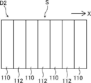
- volume hologram type diffraction element As the volume hologram type diffraction element, a known volume hologram type diffraction element can be used. As shown in D2 illustrated in FIG. 14, the volume hologram type diffraction element is configured such that a linear region 110 having a high refractive index and a linear region 112 having a low refractive index are alternately arranged in parallel at a predetermined period. It is a thing. The period of the diffraction structure, the material, the refractive index of each region, and the like may be appropriately set according to the wavelength range to be diffracted.
- the structure in which the linear region 110 having a high refractive index and the linear region 112 having a low refractive index are alternately formed is a diffraction structure, and the period of the arrangement of the region 110 and the region 112 is It is the period of the diffraction structure, and the arrangement direction of the region 110 and the region 112 shown by the arrow X in FIG. 14 is the periodic direction of the diffraction structure.
- the polarization diffraction element As the polarization diffraction element, a known polarization diffraction element can be used.
- the polarized light diffracting element is a diffraction element that controls the diffraction direction, the polarized state, and the diffracted light intensity of the emitted light according to the polarized state of the incident light by controlling the polarized state in a fine region.
- a polarized diffraction element for example, the structural double refraction described in "Erez Hasman et al., Polarization dependent focusing lens by use of quantized Pancharatnm-Berry phase diffractive optics, Applied Physics Letters, Volume 82, Number 3 pp.328-330"
- Examples thereof include a polarized diffraction element having a diffraction structure formed by using the same, a polarized diffraction element having a diffraction structure formed by using the double refraction material described in Patent No. 5276847, and the like.
- the polarization diffraction element is formed by using a composition containing a liquid crystal compound, and has a liquid crystal orientation pattern in which the direction of the optical axis derived from the liquid crystal compound changes while continuously rotating along at least one direction in the plane.
- a liquid crystal diffraction element having.
- liquid crystal diffraction element A Liquid crystal diffraction element A
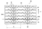
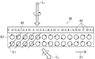
- the liquid crystal diffractometer 29 shown in FIGS. 15 and 16 has a fixed cholesteric liquid crystal phase, and the orientation of the optical axis derived from the liquid crystal compound changes while continuously rotating along at least one direction in the plane.
- the liquid crystal diffraction element 29 has a support 30, an alignment film 32, and a pattern cholesteric liquid crystal layer 34.
- the liquid crystal diffraction element 29 of the example shown in FIG. 15 has a support 30, an alignment film 32, and a pattern cholesteric liquid crystal layer 34, but the present invention is not limited thereto.
- the liquid crystal diffraction element may have, for example, only the alignment film 32 and the pattern cholesteric liquid crystal layer 34 from which the support 30 has been peeled off after being attached to the light guide plate 16.
- the liquid crystal diffraction element may have, for example, only the pattern cholesteric liquid crystal layer 34 in which the support 30 and the alignment film 32 are peeled off after being attached to the light guide plate 16.
- the support 30 supports the alignment film 32 and the pattern cholesteric liquid crystal layer 34.
- various sheet-like materials films, plate-like materials
- the support 30 has a transmittance of 50% or more, more preferably 70% or more, and further preferably 85% or more with respect to the corresponding light.
- the thickness of the support 30 is not limited, and the thickness capable of holding the alignment film 32 and the pattern cholesteric liquid crystal layer 34 can be appropriately set according to the application of the liquid crystal diffraction element, the forming material of the support 30, and the like. Just do it.
- the thickness of the support 30 is preferably 1 to 2000 ⁇ m, more preferably 3 to 500 ⁇ m, still more preferably 5 to 250 ⁇ m.
- the support 30 may be single-layered or multi-layered.
- Examples of the support 30 in the case of a single layer include a support 30 made of glass, triacetyl cellulose (TAC), polyethylene terephthalate (PET), polycarbonate, polyvinyl chloride, acrylic, polyolefin and the like.
- Examples of the support 30 in the case of a multi-layer structure include those including any of the above-mentioned single-layer supports as a substrate and providing another layer on the surface of the substrate.
- an alignment film 32 is formed on the surface of the support 30.
- the alignment film 32 is an alignment film for orienting the liquid crystal compound 40 in a predetermined liquid crystal alignment pattern when forming the pattern cholesteric liquid crystal layer 34.
- the orientation of the optical axis 40A (see FIG. 16) derived from the liquid crystal compound 40 changes while continuously rotating along one direction in the plane. Has a liquid crystal orientation pattern. Therefore, the alignment film 32 is formed so that the pattern cholesteric liquid crystal layer 34 can form this liquid crystal alignment pattern.
- “the direction of the optic axis 40A rotates” is also simply referred to as "the optical axis 40A rotates”.
- a rubbing-treated film made of an organic compound such as a polymer an oblique vapor deposition film of an inorganic compound, a film having a microgroove, and Langmuir of an organic compound such as ⁇ -tricosanoic acid, dioctadecylmethylammonium chloride and methyl stearylate.
- An example is a film obtained by accumulating LB (Langmuir-Blodgett) films produced by the Brodget method.
- the alignment film 32 by the rubbing treatment can be formed by rubbing the surface of the polymer layer with paper or cloth several times in a certain direction.
- Materials used for the alignment film 32 include polyimide, polyvinyl alcohol, polymers having a polymerizable group described in JP-A-9-152509, JP-A-2005-97377, JP-A-2005-99228, and JP-A-2005-99228. , JP-A-2005-128503, the material used for forming the alignment film 32 and the like described in JP-A-2005-128503 is preferable.
- a so-called photo-alignment film in which a photo-alignable material is irradiated with polarized light or non-polarized light to form an alignment film 32 is preferably used. That is, in the liquid crystal diffraction element 29, as the alignment film 32, a photoalignment film formed by applying a photoalignment material on the support 30 is preferably used. Polarized irradiation can be performed from a direction perpendicular to or diagonally to the photoalignment film, and non-polarized irradiation can be performed from an oblique direction to the photoalignment film.
- Examples of the photoalignment material used for the alignment film that can be used in the present invention include JP-A-2006-285197, JP-A-2007-76839, JP-A-2007-138138, and JP-A-2007-94071. , JP-A-2007-121721, JP-A-2007-140465, JP-A-2007-156439, JP-A-2007-133184, JP-A-2009-109831, Patent No. 3883848 and Patent No. 4151746.
- Photodimerizable compounds described in JP-A-147,561 and JP-A-2014-12823, particularly synnamate compounds, chalcone compounds, coumarin compounds and the like, are exemplified as preferable examples.
- azo compounds, photocrosslinkable polyimides, photocrosslinkable polyamides, photocrosslinkable polyesters, synnamet compounds, and chalcone compounds are preferably used.
- the thickness of the alignment film 32 is not limited, and the thickness at which the required alignment function can be obtained may be appropriately set according to the material for forming the alignment film 32.
- the thickness of the alignment film 32 is preferably 0.01 to 5 ⁇ m, more preferably 0.05 to 2 ⁇ m.
- the method for forming the alignment film 32 there is no limitation on the method for forming the alignment film 32, and various known methods depending on the material for forming the alignment film 32 can be used. As an example, a method in which the alignment film 32 is applied to the surface of the support 30 and dried, and then the alignment film 32 is exposed with a laser beam to form an alignment pattern is exemplified.
- FIG. 22 conceptually shows an example of an exposure apparatus that exposes the alignment film 32 to form an alignment pattern.
- the exposure apparatus 60 shown in FIG. 22 uses a light source 64 provided with a laser 62, a ⁇ / 2 plate 65 that changes the polarization direction of the laser light M emitted by the laser 62, and a laser beam M emitted by the laser 62 as a light beam MA. It includes a polarized beam splitter 68 that separates the MB into two, mirrors 70A and 70B arranged on the optical paths of the two separated rays MA and MB, respectively, and ⁇ / 4 plates 72A and 72B.
- the light source 64 emits linearly polarized light P 0 .
- lambda / 4 plate 72A is linearly polarized light P 0 (the ray MA) to the right circularly polarized light P R
- lambda / 4 plate 72B is linearly polarized light P 0 (the rays MB) to the left circularly polarized light P L, converts respectively.
- the support 30 having the alignment film 32 before the alignment pattern is formed is arranged in the exposed portion, and the two light rays MA and the light rays MB are crossed and interfere with each other on the alignment film 32, and the interference light is made to interfere with the alignment film 32. Is exposed to light. Due to the interference at this time, the polarization state of the light applied to the alignment film 32 changes periodically in the form of interference fringes. As a result, an alignment film having an alignment pattern in which the orientation state changes periodically (hereinafter, also referred to as a pattern alignment film) can be obtained.
- the period of the orientation pattern can be adjusted by changing the intersection angle ⁇ of the two rays MA and MB.
- the optical axis 40A rotates in one direction.
- the length of one cycle in which the optical shaft 40A rotates 180 ° can be adjusted.
- the optical axis 40A derived from the liquid crystal compound 40 is aligned along one direction, as will be described later.
- the pattern cholesteric liquid crystal layer 34 having a continuously rotating liquid crystal orientation pattern can be formed. Further, the rotation direction of the optical shaft 40A can be reversed by rotating the optical axes of the ⁇ / 4 plates 72A and 72B by 90 °, respectively.
- the direction of the optical axis of the liquid crystal compound in the pattern cholesteric liquid crystal layer formed on the pattern alignment film changes while continuously rotating along at least one direction in the plane. It has an orientation pattern that orients the liquid crystal compound so as to have the same liquid crystal orientation pattern.
- the axis of the pattern alignment film is the axis along the direction in which the liquid crystal compound is oriented
- the direction of the alignment axis of the pattern alignment film changes while continuously rotating along at least one direction in the plane. It can be said that it has an orientation pattern.
- the orientation axis of the pattern alignment film can be detected by measuring the absorption anisotropy. For example, when the pattern alignment film is irradiated with rotating linear polarization and the amount of light transmitted through the pattern alignment film is measured, the direction in which the amount of light is maximum or minimum gradually changes along one direction in the plane. It changes and is observed.
- the alignment film 32 is provided as a preferred embodiment and is not an essential constituent requirement.
- the pattern cholesteric liquid crystal layer is made of optics derived from the liquid crystal compound 40. It is also possible to have a configuration having a liquid crystal orientation pattern in which the orientation of the axis 40A changes while continuously rotating along at least one direction in the plane. That is, in the present invention, the support 30 may act as an alignment film.
- a pattern cholesteric liquid crystal layer 34 is formed on the surface of the alignment film 32.
- the pattern cholesteric liquid crystal layer is a cholesteric liquid crystal layer in which the cholesteric liquid crystal phase is fixed, and the direction of the optical axis derived from the liquid crystal compound rotates continuously along at least one direction in the plane. It is a cholesteric liquid crystal layer having a changing liquid crystal orientation pattern.
- the pattern cholesteric liquid crystal layer 34 has a spiral structure in which the liquid crystal compound 40 is spirally swirled and stacked in the same manner as the cholesteric liquid crystal layer formed by fixing a normal cholesteric liquid crystal phase.
- the liquid crystal compound 40 has a structure in which the liquid crystal compounds 40 spirally swirling at a plurality of pitches are laminated, with the configuration in which the liquid crystal compounds 40 are spirally rotated once (rotated 360 °) and stacked as one spiral pitch.
- the cholesteric liquid crystal layer having the cholesteric liquid crystal phase fixed has wavelength selective reflectivity.
- the selective reflection wavelength region of the cholesteric liquid crystal layer depends on the length of the spiral 1 pitch in the thickness direction (pitch P shown in FIG. 15).
- the spiral pitch P of the pattern cholesteric liquid crystal layer is adjusted for each liquid crystal diffraction element.
- the selective reflection wavelength range of the cholesteric liquid crystal layer may be appropriately set.
- the cholesteric liquid crystal phase is known to exhibit selective reflectivity at specific wavelengths.
- the selective reflection center wavelength can be adjusted by adjusting the spiral pitch. The longer the pitch P, the longer the selective reflection center wavelength of the cholesteric liquid crystal phase.
- the spiral pitch P is the spiral structure of the cholesteric liquid crystal phase for one pitch (the period of the spiral), in other words, the number of spiral turns is one, that is, the cholesteric liquid crystal phase is formed.
- This is the length in the spiral axis direction in which the director of the liquid crystal compound (in the long axis direction in the case of a rod-shaped liquid crystal) rotates 360 °.
- the spiral pitch of the cholesteric liquid crystal phase depends on the type of chiral agent used together with the liquid crystal compound and the concentration of the chiral agent added when forming the cholesteric liquid crystal layer. Therefore, by adjusting these, a desired spiral pitch can be obtained.
- pitch adjustment see Fujifilm Research Report No. 50 (2005) p. There is a detailed description in 60-63.
- For the measurement method of spiral sense and pitch use the method described in "Introduction to Liquid Crystal Chemistry Experiment", edited by Japan Liquid Crystal Society, Sigma Publishing, 2007, p. 46, and "Liquid Handbook", Liquid Liquid Handbook Editorial Committee, Maruzen, p. 196. be able to.
- the cholesteric liquid crystal phase exhibits selective reflectivity to either left or right circularly polarized light at a specific wavelength. Whether the reflected light is right-handed or left-handed depends on the twisting direction (sense) of the spiral of the cholesteric liquid crystal phase.
- the selective reflection of circular polarization by the cholesteric liquid crystal phase reflects the right circular polarization when the spiral twist direction of the cholesteric liquid crystal layer is right, and the left circular polarization when the spiral twist direction is left.
- the direction of rotation of the cholesteric liquid crystal phase can be adjusted by the type of the liquid crystal compound forming the cholesteric liquid crystal layer and / or the type of the chiral agent added.
- ⁇ n can be adjusted by the type of the liquid crystal compound forming the cholesteric liquid crystal layer, the mixing ratio thereof, and the temperature at the time of fixing the orientation.
- the half-value width of the reflection wavelength range is adjusted according to the application of the diffractive element, and may be, for example, 10 to 500 nm, preferably 20 to 300 nm, and more preferably 30 to 100 nm.
- the pattern cholesteric liquid crystal layer can be formed by fixing the cholesteric liquid crystal phase in a layered manner.
- the structure in which the cholesteric liquid crystal phase is fixed may be a structure in which the orientation of the liquid crystal compound that is the cholesteric liquid crystal phase is maintained, and typically, the polymerizable liquid crystal compound is placed in the orientation state of the cholesteric liquid crystal phase. Therefore, it is preferable that the structure is polymerized and cured by irradiation with ultraviolet rays, heating, etc. to form a non-fluid layer, and at the same time, the structure is changed to a state in which the orientation form is not changed by an external field or an external force.
- the polymerizable liquid crystal compound may lose its liquid crystal property by increasing its molecular weight by a curing reaction.
- An example of a material used for forming a pattern cholesteric liquid crystal layer in which a cholesteric liquid crystal phase is fixed is a liquid crystal composition containing a liquid crystal compound.
- the liquid crystal compound is preferably a polymerizable liquid crystal compound.
- the liquid crystal composition used for forming the pattern cholesteric liquid crystal layer may further contain a surfactant and a chiral agent.
- the polymerizable liquid crystal compound may be a rod-shaped liquid crystal compound or a disk-shaped liquid crystal compound.
- the rod-shaped polymerizable liquid crystal compound forming the cholesteric liquid crystal phase include a rod-shaped nematic liquid crystal compound.
- rod-shaped nematic liquid crystal compound examples include azomethines, azoxys, cyanobiphenyls, cyanophenyl esters, benzoic acid esters, cyclohexanecarboxylic acid phenyl esters, cyanophenylcyclohexanes, cyano-substituted phenylpyrimidines, and alkoxy-substituted phenylpyrimidines.
- Phenyldioxans, trans, alkenylcyclohexylbenzonitriles and the like are preferably used. Not only low molecular weight liquid crystal compounds but also high molecular weight liquid crystal compounds can be used.
- the polymerizable liquid crystal compound is obtained by introducing a polymerizable group into the liquid crystal compound.
- the polymerizable group include an unsaturated polymerizable group, an epoxy group, and an aziridinyl group, and an unsaturated polymerizable group is preferable, and an ethylenically unsaturated polymerizable group is more preferable.
- the polymerizable group can be introduced into the molecule of the liquid crystal compound by various methods.
- the number of polymerizable groups contained in the polymerizable liquid crystal compound is preferably 1 to 6, more preferably 1 to 3.
- Examples of polymerizable liquid crystal compounds include Makromol. Chem. , 190, 2255 (1989), Advanced Materials 5, 107 (1993), US Pat. No.
- a cyclic organopolysiloxane compound having a cholesteric phase as disclosed in Japanese Patent Application Laid-Open No. 57-165480 can be used.
- a polymer liquid crystal compound a polymer having a mesogen group exhibiting liquid crystal introduced at the main chain, a side chain, or both the main chain and the side chain, and a polymer cholesteric having a cholesteryl group introduced into the side chain.
- a liquid crystal, a liquid crystal polymer as disclosed in JP-A-9-133810, a liquid crystal polymer as disclosed in JP-A-11-293252, and the like can be used.
- disk-shaped liquid crystal compound As the disk-shaped liquid crystal compound, for example, those described in JP-A-2007-108732 and JP-A-2010-244038 can be preferably used.
- the amount of the polymerizable liquid crystal compound added to the liquid crystal composition is preferably 75 to 99.9% by mass, preferably 80 to 99%, based on the solid content mass (mass excluding the solvent) of the liquid crystal composition. It is more preferably mass%, and even more preferably 85-90 mass%.
- the liquid crystal composition used for forming the pattern cholesteric liquid crystal layer may contain a surfactant.
- the surfactant is preferably a compound that can function as an orientation control agent that contributes to the orientation of the cholesteric liquid crystal phase in a stable or rapid manner.
- examples of the surfactant include a silicone-based surfactant and a fluorine-based surfactant, and a fluorine-based surfactant is preferably exemplified.
- the surfactant include the compounds described in paragraphs [802] to [0090] of JP2014-119605, and the compounds described in paragraphs [0031] to [0034] of JP2012-203237. , The compounds exemplified in paragraphs [0092] and [093] of JP-A-2005-999248, paragraphs [0076] to [0078] and paragraphs [0082]-[0085] of JP-A-2002-129162. Examples thereof include the compounds exemplified in the above, and fluorine (meth) acrylate-based polymers described in paragraphs [0018] to [0043] of JP-A-2007-272185.
- the surfactant one type may be used alone, or two or more types may be used in combination.
- the fluorine-based surfactant the compounds described in paragraphs [2002] to [0090] of JP-A-2014-119605 are preferable.
- the amount of the surfactant added to the liquid crystal composition is preferably 0.01 to 10% by mass, more preferably 0.01 to 5% by mass, and 0.02 to 1% by mass with respect to the total mass of the liquid crystal compound. Is even more preferable.
- the chiral agent has a function of inducing a helical structure of a cholesteric liquid crystal phase. Since the twist direction or the spiral pitch of the spiral induced by the compound is different, the chiral agent may be selected according to the purpose.
- the chiral agent is not particularly limited, and is known as a compound (for example, Liquid Crystal Device Handbook, Chapter 3, Section 4-3, TN (twisted nematic), STN (Super Twisted Nematic) chiral agent, page 199, Japan Science Promotion. The 142nd Committee of the Society, 1989), isosorbide, isomannide derivatives and the like can be used.
- the chiral agent generally contains an asymmetric carbon atom, but an axial asymmetric compound or a surface asymmetric compound that does not contain an asymmetric carbon atom can also be used as the chiral agent.
- Examples of axially asymmetric or surface asymmetric compounds include binaphthyl, helicene, paracyclophane, and derivatives thereof.
- the chiral agent may have a polymerizable group. When both the chiral agent and the liquid crystal compound have a polymerizable group, the repeating unit derived from the polymerizable liquid crystal compound and the repeating unit derived from the chiral agent are derived by the polymerization reaction between the polymerizable chiral agent and the polymerizable liquid crystal compound.
- the polymerizable group of the polymerizable chiral agent is preferably a group of the same type as the polymerizable group of the polymerizable liquid crystal compound. Therefore, the polymerizable group of the chiral agent is preferably an unsaturated polymerizable group, an epoxy group or an aziridinyl group, more preferably an unsaturated polymerizable group, and preferably an ethylenically unsaturated polymerizable group. More preferred. Moreover, the chiral agent may be a liquid crystal compound.
- the chiral agent has a photoisomerizing group
- a pattern of a desired reflection wavelength corresponding to the emission wavelength can be formed by irradiation with a photomask such as active light after coating and orientation.
- a photomask such as active light after coating and orientation.
- an isomerization site of a compound exhibiting photochromic properties, an azo group, an azoxy group, or a cinnamoyl group is preferable.
- Specific compounds include JP-A-2002-80478, JP-A-2002-80851, JP-A-2002-179668, JP-A-2002-179669, JP-A-2002-179670, and JP-A-2002.
- the content of the chiral agent in the liquid crystal composition is preferably 0.01 to 200 mol%, more preferably 1 to 30 mol%, based on the molar content of the liquid crystal compound.
- the liquid crystal composition contains a polymerizable compound, it preferably contains a polymerization initiator.
- the polymerization initiator used is preferably a photopolymerization initiator capable of initiating the polymerization reaction by irradiation with ultraviolet rays.
- photopolymerization initiators include ⁇ -carbonyl compounds (described in U.S. Pat. No. 2,376,661 and U.S. Pat. No. 2,376,670), acidoin ethers (described in U.S. Pat. No. 2,448,828), and ⁇ -hydrogen.
- Substituted aromatic acidoine compounds (described in US Pat. No. 2722512), polynuclear quinone compounds (described in US Pat. Nos. 3046127 and US Pat. No. 2951758), triarylimidazole dimers and p-aminophenyl ketone. Combinations (described in US Pat. No. 3,549,637), aclysine and phenazine compounds (Japanese Patent Laid-Open No. 60-105667, US Pat. No. 4,239,850), and oxadiazole compounds (US Pat. No. 421,970). Description) and the like.
- the content of the photopolymerization initiator in the liquid crystal composition is preferably 0.1 to 20% by mass, more preferably 0.5 to 12% by mass, based on the content of the liquid crystal compound.
- the liquid crystal composition may optionally contain a cross-linking agent in order to improve the film strength and durability after curing.
- a cross-linking agent one that cures with ultraviolet rays, heat, moisture, or the like can be preferably used.
- the cross-linking agent is not particularly limited and may be appropriately selected depending on the intended purpose. For example, a polyfunctional acrylate compound such as trimethylpropantri (meth) acrylate and pentaerythritol tri (meth) acrylate; glycidyl (meth) acrylate.
- epoxy compounds such as ethylene glycol diglycidyl ether; aziridine compounds such as 2,2-bishydroxymethylbutanol-tris [3- (1-aziridinyl) propionate] and 4,4-bis (ethyleneiminocarbonylamino) diphenylmethane; hexa Isocyanate compounds such as methylenediisocyanate and biuret-type isocyanate; polyoxazoline compounds having an oxazoline group in the side chain; and alkoxysilane compounds such as vinyltrimethoxysilane and N- (2-aminoethyl) 3-aminopropyltrimethoxysilane. Can be mentioned.
- a known catalyst can be used depending on the reactivity of the cross-linking agent, and the productivity can be improved in addition to the improvement of the film strength and durability. These may be used alone or in combination of two or more.
- the content of the cross-linking agent is preferably 3 to 20% by mass, more preferably 5 to 15% by mass, based on the solid content mass of the liquid crystal composition. When the content of the cross-linking agent is within the above range, the effect of improving the cross-linking density can be easily obtained, and the stability of the cholesteric liquid crystal phase is further improved.
- liquid crystal composition if necessary, a polymerization inhibitor, an antioxidant, an ultraviolet absorber, a light stabilizer, a coloring material, metal oxide fine particles, etc. are added in a range that does not deteriorate the optical performance and the like. Can be added with.
- the liquid crystal composition is preferably used as a liquid when forming the pattern cholesteric liquid crystal layer.
- the liquid crystal composition may contain a solvent.
- the solvent is not limited and may be appropriately selected depending on the intended purpose, but an organic solvent is preferable.
- the organic solvent is not limited and may be appropriately selected depending on the intended purpose.
- the liquid crystal composition When forming the pattern cholesteric liquid crystal layer, the liquid crystal composition is applied to the forming surface of the pattern cholesteric liquid crystal layer, the liquid crystal compound is oriented in the state of the cholesteric liquid crystal phase, and then the liquid crystal compound is cured to obtain the pattern cholesteric liquid crystal. It is preferably a layer. That is, when the pattern cholesteric liquid crystal layer is formed on the alignment film 32, the liquid crystal composition is applied to the alignment film 32, the liquid crystal compound is oriented in the state of the cholesteric liquid crystal phase, and then the liquid crystal compound is cured. It is preferable to form a pattern cholesteric liquid crystal layer in which the cholesteric liquid crystal phase is fixed.
- printing methods such as inkjet and scroll printing, and known methods such as spin coating, bar coating and spray coating that can uniformly apply the liquid to a sheet-like material can be used.
- the applied liquid crystal composition is dried and / or heated as needed and then cured to form a pattern cholesteric liquid crystal layer.
- the liquid crystal compound in the liquid crystal composition may be oriented to the cholesteric liquid crystal phase.
- the heating temperature is preferably 200 ° C. or lower, more preferably 130 ° C. or lower.
- the oriented liquid crystal compound is further polymerized, if necessary.
- the polymerization may be either thermal polymerization or photopolymerization by light irradiation, but photopolymerization is preferable.
- the irradiation energy is preferably 20mJ / cm 2 ⁇ 50J / cm 2, more preferably 50 ⁇ 1500mJ / cm 2.
- light irradiation may be carried out under heating conditions or a nitrogen atmosphere.
- the wavelength of the ultraviolet rays to be irradiated is preferably 250 to 430 nm.
- the thickness of the pattern cholesteric liquid crystal layer is not limited, and is required depending on the application of the liquid crystal diffraction element 29, the light reflectance required for the pattern cholesteric liquid crystal layer, the material for forming the pattern cholesteric liquid crystal layer, and the like.
- the thickness at which the light reflectance can be obtained may be appropriately set.
- Pattern LCD alignment pattern of cholesteric liquid crystal layer As described above, in the liquid crystal diffractometer 29, in the pattern cholesteric liquid crystal layer, the orientation of the optical axis 40A derived from the liquid crystal compound 40 forming the cholesteric liquid crystal phase is continuous in one direction in the plane of the pattern cholesteric liquid crystal layer. It has a liquid crystal orientation pattern that changes while rotating.
- the optical axis 40A derived from the liquid crystal compound 40 is a so-called slow-phase axis having the highest refractive index in the liquid crystal compound 40.
- the optical shaft 40A is along the long axis direction of the rod shape.
- the optical axis 40A derived from the liquid crystal compound 40 is also referred to as "optical axis 40A of liquid crystal compound 40" or "optical axis 40A".
- FIG. 16 conceptually shows a plan view of the pattern cholesteric liquid crystal layer 34.
- the liquid crystal compound 40 shows only the liquid crystal compound 40 on the surface of the alignment film 32.
- the liquid crystal compound 40 constituting the pattern cholesteric liquid crystal layer 34 is placed in the plane of the liquid crystal diffractometer 29 according to the alignment pattern formed on the lower alignment film 32.
- the optical axis 40A of the liquid crystal compound 40 has a liquid crystal orientation pattern that changes while continuously rotating clockwise along the arrow X1 direction.
- the liquid crystal compound 40 constituting the pattern cholesteric liquid crystal layer 34 is in a state of being two-dimensionally arranged in the direction orthogonal to the arrow X1 and this one direction (arrow X1 direction).
- the direction orthogonal to the arrow X1 direction is conveniently referred to as the Y direction. That is, the arrow Y direction is a direction in which the direction of the optical axis 40A of the liquid crystal compound 40 is orthogonal to one direction that changes while continuously rotating in the plane of the pattern cholesteric liquid crystal layer. Therefore, in FIG. 15 and FIG. 17 described later, the Y direction is a direction orthogonal to the paper surface.
- the fact that the direction of the optical axis 40A of the liquid crystal compound 40 changes while continuously rotating in the arrow X1 direction specifically means that the liquid crystal compounds arranged along the arrow X1 direction.
- the angle formed by the optical axis 40A of 40 and the direction of arrow X1 differs depending on the position in the direction of arrow X1, and the angle formed by the optical axis 40A and the direction of arrow X1 along the direction of arrow X1 is ⁇ to ⁇ + 180 ° or It means that the temperature is gradually changing up to ⁇ -180 °.
- the difference in the angles of the optical axes 40A of the liquid crystal compounds 40 adjacent to each other in the arrow X1 direction is preferably 45 ° or less, more preferably 15 ° or less, and further preferably a smaller angle. ..
- the liquid crystal compound 40 forming the pattern cholesteric liquid crystal layer 34 has the direction of the optical axis 40A in the Y direction orthogonal to the arrow X1 direction, that is, in the Y direction orthogonal to one direction in which the optical axis 40A continuously rotates. equal.
- the liquid crystal compound 40 forming the pattern cholesteric liquid crystal layer 34 has the same angle formed by the optical axis 40A of the liquid crystal compound 40 and the arrow X1 direction in the Y direction.
- the optical axis 40A of the liquid crystal compound 40 is 180 ° in the direction of the arrow X1 in which the optical axis 40A continuously rotates and changes in the plane.
- the length of rotation (distance) be the length ⁇ of one cycle in the liquid crystal alignment pattern. That is, the distance between the centers of the two liquid crystal compounds 40 having the same angle with respect to the arrow X1 direction in the arrow X1 direction is defined as the length ⁇ of one cycle.
- the distance between the centers of the two liquid crystal compounds 40 in which the direction of the arrow X1 and the direction of the optical axis 40A coincide with each other in the direction of the arrow X1 is defined as the length ⁇ of one cycle. .. In the following description, the length ⁇ of this one cycle is also referred to as "one cycle ⁇ ".
- the liquid crystal alignment pattern of the pattern cholesteric liquid crystal layer 34 repeats this one cycle ⁇ in the direction of arrow X1, that is, in one direction in which the direction of the optical axis 40A continuously rotates and changes.
- the pattern cholesteric liquid crystal layer formed by fixing the cholesteric liquid crystal phase usually specularly reflects the incident light (circularly polarized light).
- the pattern cholesteric liquid crystal layer 34 reflects the incident light at an angle X1 direction with respect to specular reflection.
- the pattern cholesteric liquid crystal layer 34 has a liquid crystal orientation pattern in which the optical axis 40A changes while continuously rotating along the arrow X1 direction (a predetermined one direction) in the plane.
- a pattern cholesteric liquid crystal layer 34 is a patterned cholesteric liquid crystal layer that selectively reflects right-circularly polarized light R R of the red light. Therefore, when light in the pattern cholesteric liquid crystal layer 34 enters the pattern cholesteric liquid crystal layer 34 reflects only right circularly polarized light R R of the red light, and transmits light of other wavelengths.
- the right circularly polarized light R R of the red light incident on the patterned cholesteric liquid crystal layer 34 periodic absolute phase in the arrow X1 direction corresponding to the orientation of the respective optical axes 40A Q is given. Further, the direction of the optical axis 40A of the liquid crystal compound 40 with respect to the arrow X1 direction is uniform in the arrangement of the liquid crystal compound 40 in the Y direction orthogonal to the arrow X1 direction. In this way the pattern cholesteric liquid crystal layer 34, for the right circularly polarized light R R of the red light, the equiphase plane E which is inclined in the arrow X1 direction to the XY plane is formed.
- the right circularly polarized light R R of the red light is reflected in the normal direction equiphase plane E, the right circularly polarized light R R of the reflected red light, with respect to the XY plane (major surface of the cholesteric liquid crystal layer) It is reflected in the direction tilted in the direction of the arrow X1.
- the arrow X1 direction optical axis 40A is unidirectional rotating, as appropriate, by setting, adjustable reflecting direction of the right-handed circularly polarized light R R of the red light. That is, if the arrow X1 direction in the opposite direction, the direction the reflection of right-handed circularly polarized light R R of the red light is also in a direction opposite to the FIGS.
- the rotation direction of the optical axis 40A of the liquid crystal compound 40 towards the direction of the arrow X1 by reversing can the reflection direction of the right circularly polarized light R R of the red light in the opposite. That is, in FIG. 16 and FIG. 17, the rotational direction of the optical axis 40A toward the arrow X1 direction in the clockwise, the right circularly polarized light R R of the red light is reflected by tilting in the arrow X1 direction, which the counterclockwise with around right circularly polarized light R R of the red light is reflected by tilting in the arrow X1 direction and the opposite direction.
- the reflection direction is reversed depending on the spiral turning direction of the liquid crystal compound 40, that is, the turning direction of the reflected circularly polarized light.
- the spiral turning direction is twisted to the right and the right circular polarization is selectively reflected, and the liquid crystal orientation in which the optical axis 40A rotates clockwise along the arrow X1 direction.
- the right circular polarization is tilted and reflected in the direction of the arrow X1.
- the pattern cholesteric liquid crystal layer has a liquid crystal orientation pattern in which the turning direction of the spiral is twisted to the left and the left circular polarization is selectively reflected, and the optical axis 40A rotates clockwise along the arrow X1 direction.
- the left circular polarization is reflected by tilting it in the direction opposite to the arrow X1 direction.
- the liquid crystal alignment pattern of the liquid crystal compound in which the optical axis of the liquid crystal compound changes while rotating along one direction in the plane is a diffraction structure, and in the liquid crystal alignment pattern of the liquid crystal compound, the optics of the liquid crystal compound.
- the length of rotation of the axis by 180 ° is the period of the diffraction structure, and one direction in which the optical axis of the liquid crystal compound changes while rotating is the period direction of the diffraction structure.
- the shorter one cycle ⁇ the larger the angle of the reflected light with respect to the above-mentioned incident light. That is, the shorter one cycle ⁇ is, the more the reflected light can be tilted and reflected with respect to the incident light.
- the pattern cholesteric liquid crystal layer is used as the liquid crystal diffraction element, but in the liquid crystal diffraction element used in the present invention, the optical axis 40A derived from the liquid crystal compound 40 is continuous along at least one direction in the plane.
- Various liquid crystal diffraction elements can be used as long as they have a liquid crystal alignment pattern that is rotating.
- the liquid crystal diffraction element may have a configuration in which the liquid crystal compound is twisted and rotated in the thickness direction to the extent that the liquid crystal compound does not become a cholesteric liquid crystal phase.
- the liquid crystal diffraction element 35 shown in FIGS. 18 and 19 has a support 30, an alignment film 32, and a pattern liquid crystal layer 36.
- the pattern liquid crystal layer 36 of the liquid crystal diffraction element 35 also has a liquid crystal orientation pattern in which the optical axis 40A of the liquid crystal compound 40 continuously rotates along the arrow X1 direction, similarly to the pattern cholesteric liquid crystal layer 34.
- FIG. 19 also shows only the liquid crystal compound on the surface of the alignment film 32, as in FIG. 16 described above.
- the liquid crystal compound 40 forming the pattern liquid crystal layer 36 is not spirally twisted and rotated in the thickness direction, and the optical axis 40A is located at the same position in the plane direction.
- Such a liquid crystal layer can be formed by not adding a chiral agent to the liquid crystal composition in the formation of the pattern cholesteric liquid crystal layer described above.
- the pattern liquid crystal layer 36 is a liquid crystal in which the direction of the optical axis 40A derived from the liquid crystal compound 40 changes while continuously rotating in the direction of arrow X, that is, in one direction indicated by arrow X. It has an orientation pattern.
- the liquid crystal compound 40 forming the pattern liquid crystal layer 36 is a liquid crystal having the same direction of the optical axis 40A in the Y direction orthogonal to the arrow X1 direction, that is, the Y direction orthogonal to one direction in which the optical axis 40A continuously rotates.
- the compounds 40 are evenly spaced.
- the angles formed by the direction of the optical axis 40A and the direction of the arrow X1 are equal between the liquid crystal compounds 40 arranged in the Y direction.
- the liquid crystal compounds arranged in the Y direction have the same angle formed by the optical axis 40A and the arrow X direction (one direction in which the direction of the optical axis of the liquid crystal compound 40 rotates).
- the region where the liquid crystal compound 40 having the same angle formed by the optical axis 40A and the arrow X direction is arranged in the Y direction is defined as the region R.
- the value of the in-plane retardation (Re) in each region R is preferably half wavelength, that is, ⁇ / 2.
- the difference in refractive index due to the refractive index anisotropy of the region R in the optically anisotropic layer is the refractive index in the direction of the slow axis in the plane of the region R and the direction orthogonal to the direction of the slow axis. It is a refractive index difference defined by the difference from the refractive index of. That is, the refractive index difference ⁇ n due to the refractive index anisotropy of the region R is the refractive index of the liquid crystal compound 40 in the direction of the optic axis 40A and the liquid crystal compound 40 in the plane of the region R in the direction perpendicular to the optical axis 40A. Equal to the difference from the refractive index. That is, the refractive index difference ⁇ n is equal to the refractive index difference of the liquid crystal compound 40.
- the incident light L 1 When the light L 1 is incident, the incident light L 1 is given a phase difference of 180 ° by passing through the pattern liquid crystal layer 36, and the transmitted light L 2 is converted into right circular polarization. Further, when the incident light L 1 passes through the pattern liquid crystal layer 36, its absolute phase changes according to the direction of the optical axis 40A of each liquid crystal compound 40. At this time, since the direction of the optical axis 40A changes while rotating along the arrow X direction, the amount of change in the absolute phase of the incident light L 1 differs depending on the direction of the optical axis 40A.
- the liquid crystal alignment pattern formed on the pattern liquid crystal layer 36 is a periodic pattern in the direction of the arrow X
- the incident light L 1 passing through the pattern liquid crystal layer 36 has a respective pattern as shown in FIG.
- a periodic absolute phase Q1 is given in the direction of arrow X corresponding to the direction of the optical axis 40A.
- the equiphase plane E1 inclined in the direction opposite to the arrow X direction is formed. Therefore, the transmitted light L 2 is refracted so as to be inclined in a direction perpendicular to the equiphase plane E 1 , and travels in a direction different from the traveling direction of the incident light L 1 .
- the left circularly polarized incident light L 1 is converted into the right circularly polarized transmitted light L 2 tilted by a certain angle in the arrow X direction with respect to the incident direction.
- the amount of change in the absolute phase of the incident light L 4 differs depending on the direction of the optical axis 40A.
- the liquid crystal alignment pattern formed on the pattern liquid crystal layer 36 is a periodic pattern in the arrow X direction
- the incident light L 4 passing through the pattern liquid crystal layer 36 has its own optics as shown in FIG.
- a periodic absolute phase Q2 is given in the direction of arrow X corresponding to the direction of the axis 40A.
- the incident light L 4 are, because it is right circularly polarized light, periodic absolute phase Q2 in the arrow X direction corresponding to the direction of the optical axis 40A is opposite to the incident light L 1 is a left-handed circularly polarized light .
- the incident light L 4 forms an equiphase plane E 2 inclined in the direction of the arrow X, which is opposite to the incident light L 1 . Therefore, the incident light L 4 is refracted so as to be inclined in a direction perpendicular to the equiphase plane E2, and travels in a direction different from the traveling direction of the incident light L 4 . In this way, the incident light L 4 is converted into left circularly polarized transmitted light L 5 tilted by a certain angle in the direction opposite to the arrow X direction with respect to the incident direction.
- the pattern liquid crystal layer 36 can also adjust the refraction angles of the transmitted lights L 2 and L 5 by changing one cycle ⁇ of the formed liquid crystal alignment pattern. Specifically, as the pattern liquid crystal layer 36 also has a shorter one cycle ⁇ of the liquid crystal alignment pattern, the light passing through the liquid crystal compounds 40 adjacent to each other strongly interferes with each other, so that the transmitted lights L 2 and L 5 are greatly refracted. be able to. Further, by making the rotation direction of the optical axis 40A of the liquid crystal compound 40, which rotates along the arrow X1 direction, the opposite direction, the refraction direction of the transmitted light can be made in the opposite direction. That is, in the examples shown in FIGS. 18 to 21, the rotation direction of the optical shaft 40A in the direction of arrow X is clockwise, but by making this rotation direction counterclockwise, the direction of refraction of transmitted light can be changed. Can be done in the opposite direction.
- the liquid crystal diffraction element having a region in which the liquid crystal compound is twisted and rotated (twist angle is less than 360 °) is used. It is preferable to use it.
- the pattern cholesteric liquid crystal layer 34 shown in FIG. 15 and the pattern liquid crystal layer 36 shown in FIG. 18 each showed a configuration in which the optical axis of the liquid crystal compound was parallel to the main surface of the liquid crystal layer (liquid crystal diffraction element).
- the optical axis of the liquid crystal compound was parallel to the main surface of the liquid crystal layer (liquid crystal diffraction element).
- the optical axis of the liquid crystal compound may be inclined to the main surface of the liquid crystal layer (liquid crystal diffraction element).
- the optical axis of the liquid crystal compound may be inclined to the main surface of the liquid crystal layer (liquid crystal diffraction element) in the above-mentioned pattern liquid crystal layer.
- these liquid crystal layers have the above-mentioned pattern cholesteric liquid crystal layer in that the orientation of the optical axis derived from the liquid crystal compound changes while continuously rotating along one direction in the plane.
- the plan view of the pattern cholesteric liquid crystal layer 34b and the plan view of the pattern liquid crystal layer 36b are the same as those in FIG.
- a configuration in which the optical axis of the liquid crystal compound is inclined toward the main surface of the liquid crystal layer (liquid crystal diffraction element) is also referred to as having a pretilt angle.
- the liquid crystal layer may have a configuration in which the optical axis of the liquid crystal compound has a pretilt angle at one interface of the upper and lower interfaces, or may have a configuration having a pretilt angle at both interfaces. Further, the pretilt angle may be different at both interfaces.
- the liquid crystal layer has a pre-tilt angle on the surface, even a bulk portion further away from the surface is affected by the surface and has a tilt angle.
- pre-tilting (tilting) the liquid crystal compound in this way the birefringence of the liquid crystal compound, which is effective when light is diffracted, is increased, and the diffraction efficiency can be improved.
- the pre-tilt angle can be measured by dividing the liquid crystal layer with a microtome and observing the cross section with a polarization microscope.
- the light vertically incident on the liquid crystal diffraction element travels diagonally in the liquid crystal layer with a bending force applied.
- a diffraction loss occurs because a deviation from conditions such as a diffraction period originally set so as to obtain a desired diffraction angle with respect to vertical incident occurs.
- the liquid crystal compound is tilted, there is an orientation in which a higher double refractive index is generated with respect to the orientation in which the light is diffracted as compared with the case where the liquid crystal compound is not tilted.
- the birefringence which is the difference between the abnormal light refractive index and the normal light refractive index.
- a liquid crystal compound having a pre-tilt angle is used. In this case, it is considered that higher diffraction efficiency can be obtained.
- the pre-tilt angle is controlled by the treatment of the interface of the liquid crystal layer.
- the pretilt angle of the liquid crystal compound can be controlled by performing a pretilt treatment on the alignment film. For example, when the alignment film is formed, the alignment film is exposed to ultraviolet rays from the front and then obliquely exposed, so that a pretilt angle can be generated in the liquid crystal compound in the liquid crystal layer formed on the alignment film. In this case, the liquid crystal compound is pre-tilted in a direction in which the uniaxial side can be seen with respect to the second irradiation direction.
- liquid crystal compound in the direction perpendicular to the second irradiation direction does not pre-tilt, there are an in-plane pre-tilt region and a non-pre-tilt region. This contributes to increasing the birefringence most in that direction when the light is diffracted in the target direction, and is therefore suitable for increasing the diffraction efficiency.
- an additive that promotes the pretilt angle can be added in the liquid crystal layer or the alignment film. In this case, an additive can be used as a factor for further increasing the diffraction efficiency. This additive can also be used to control the pretilt angle of the interface on the air side.
- the in-plane retardation Re is measured in the normal direction and the direction inclined with respect to the normal, the in-plane retardation Re is generated in either the slow phase axial plane or the advancing axial plane. It is preferable that the absolute value of the measurement angle whose minimum direction is the normal is 5 ° or more.
- the liquid crystal compound of the pattern cholesteric liquid crystal layer is inclined with respect to the main surface, and the inclination direction substantially coincides with the bright and dark lines of the cholesteric liquid crystal phase.
- the normal direction is a direction orthogonal to the main surface. Since the pattern cholesteric liquid crystal layer has such a configuration, circular polarization can be diffracted with higher diffraction efficiency as compared with the pattern cholesteric liquid crystal layer in which the liquid crystal compound is parallel to the main surface as shown in FIG.
- the liquid crystal compound of the pattern cholesteric liquid crystal layer is inclined with respect to the main surface and the inclination direction substantially coincides with the bright and dark lines of the cholesteric liquid crystal phase
- the bright and dark areas corresponding to the reflecting surface and the liquid crystal The optical axis of the compound is aligned. Therefore, the action of the liquid crystal compound on the reflection (diffraction) of light is increased, and the diffraction efficiency can be improved. As a result, the amount of reflected light with respect to the incident light can be further improved.
- the absolute value of the optical axis tilt angle of the pattern cholesteric liquid crystal layer is 5 ° or more, preferably 15 ° or more, and more preferably 20 ° or more.
- any of a surface relief type diffraction element, a volume hologram type diffraction element, and a polarization diffraction element may be used as each diffraction element.
- different types of diffraction elements may be used in combination.
- a surface relief type diffraction element may be used as the incident diffraction element
- a polarization diffraction element liquid crystal diffraction element
- Different types of diffraction elements may be used for the first incident diffraction element and the second incident diffraction element.
- different types of diffraction elements may be used between the first intermediate diffraction element and the second intermediate diffraction element, and the first emission diffraction element and the second emission diffraction element.
- the light guide element and the image display device of the present invention may use a diffraction optical method for enlarging the exit pupil in order to improve visibility.
- a diffraction optical method for enlarging the exit pupil in order to improve visibility.
- an optical method using a plurality of diffraction elements that is, a diffraction optical method including an inner coupling, intermediate and outer coupling diffraction elements can be used. This method is described in detail in Japanese Patent Application Laid-Open No. 2008-546020.
- the present invention is not limited to the above-mentioned examples, and various improvements and changes may be made without departing from the gist of the present invention. Of course, it's good.
- Example 1 ⁇ Manufacturing of incident diffraction element G> (Formation of alignment film) A glass substrate was prepared as a support. The following coating liquid for forming an alignment film was applied onto the support by spin coating. The support on which the coating liquid for forming the alignment film was formed was dried on a hot plate at 60 ° C. for 60 seconds to form an alignment film.
- the alignment film was exposed using the exposure apparatus shown in FIG. 22 to form an alignment film P-1 having an alignment pattern.
- a laser that emits laser light having a wavelength (325 nm) was used.
- the exposure amount due to the interference light was set to 1000 mJ / cm 2 .
- One cycle (the length of rotation of the optical axis by 180 °) of the orientation pattern formed by the interference between the two laser beams was controlled by changing the intersection angle (intersection angle ⁇ ) of the two lights.
- composition A-1 (Formation of pattern cholesteric liquid crystal layer) The following composition A-1 was prepared as the liquid crystal composition forming the first incident diffraction element.
- This composition A-1 is a liquid crystal composition that forms a cholesteric liquid crystal layer (cholesteric liquid crystal phase) that reflects right circularly polarized light.
- composition A-1 is applied onto the alignment film P-1, the coating film is heated to 80 ° C. on a hot plate, and then the wavelength is 365 nm using a high-pressure mercury lamp at 80 ° C. under a nitrogen atmosphere.
- the orientation of the liquid crystal compound was fixed, and a pattern cholesteric liquid crystal layer (first layer) of the first incident diffraction element was formed.
- the thickness surface pitch in the normal direction (thickness direction) with respect to the main surface was 8 pitches.
- the interval in the normal direction from the bright part to the bright part or from the dark part to the main surface of the dark part was set to 1/2 surface pitch.
- the inclined surface pitch of the inclined surface of the bright part and the dark part with respect to the main surface was 0.39 ⁇ m.
- the interval in the normal direction from the bright part to the bright part or from the dark part to the dark part in the normal direction was defined as a 1/2 surface pitch.
- the bright and dark areas referred to here are bright and dark areas derived from the cholesteric liquid crystal phase, which are seen when the cross section of the cholesteric liquid crystal layer is observed by SEM.
- the chiral agent Ch-1 was changed to 4.31 parts by mass and the film thickness was adjusted in the same manner, except that the pattern cholesteric liquid crystal layer (2) was placed on the pattern cholesteric liquid crystal layer (first layer). Layer) was formed.
- the thickness surface pitch was 8 pitches and the inclined surface pitch was 0.44 ⁇ m.
- one cycle in which the optical axis of the liquid crystal compound was rotated by 180 ° was 0.43 ⁇ m.
- the amount of chiral agent in the composition was changed to 4.12 parts by mass
- the amount of chiral agent in the composition forming the pattern cholesteric liquid crystal layer (second layer) was changed to 3.52 parts by mass
- the film thickness was adjusted.
- the thickness plane pitch of the pattern cholesteric liquid crystal layer (first layer) and the pattern cholesteric liquid crystal layer (second layer) of the incident diffraction element R is 8 pitches, and in the liquid crystal alignment pattern, one cycle in which the optical axis of the liquid crystal compound rotates 180 ° is , 0.51 ⁇ m.
- the inclined surface pitch of the pattern cholesteric liquid crystal layer (first layer) was 0.46 ⁇ m, and the inclined surface pitch of the pattern cholesteric liquid crystal layer (second layer) was 0.53 ⁇ m.
- An intermediate diffraction element G was produced in the same manner as the incident diffraction element G except that the amount of the chiral agent in the above was changed to 4.75 parts by mass and the film thickness was adjusted.
- the second pattern cholesteric liquid crystal layer was not formed.
- the thickness plane pitch of the pattern cholesteric liquid crystal layer (first layer) of the intermediate diffraction element G was 2 pitches, and in the liquid crystal alignment pattern, one cycle in which the optical axis of the liquid crystal compound was rotated by 180 ° was 0.23 ⁇ m.
- the inclined surface pitch of the pattern cholesteric liquid crystal layer (first layer) was 0.40 ⁇ m.
- An intermediate diffraction element R was produced in the same manner as the incident diffraction element R except that the amount of the chiral agent in the above was changed to 4.42 parts by mass and the film thickness was adjusted. The second pattern cholesteric liquid crystal layer was not formed.
- the thickness plane pitch of the pattern cholesteric liquid crystal layer (first layer) of the intermediate diffraction element R was 2 pitches, and in the liquid crystal alignment pattern, one cycle in which the optical axis of the liquid crystal compound was rotated by 180 ° was 0.28 ⁇ m.
- the inclined surface pitch of the pattern cholesteric liquid crystal layer (first layer) was 0.43 ⁇ m.
- the emission diffraction element G and the emission diffraction element R were manufactured in the same manner as the incident diffraction element G and the incident diffraction element R, respectively, except that the film thickness was adjusted.
- the thickness surface pitch of each pattern cholesteric liquid crystal layer (first layer) and pattern cholesteric liquid crystal layer (second layer) was 2 pitches.
- a light guide plate having a size of 60 mm ⁇ 70 mm, a thickness of 1 mm, and a material: glass was used.
- An incident diffraction element G is used as the first incident diffraction element
- an incident diffraction element R is used as the second incident diffraction element
- an intermediate diffraction element G is used as the first intermediate diffraction element
- an intermediate diffraction element R is used as the second intermediate diffraction element.
- the exit diffraction element G was used as the first exit diffraction element
- the exit diffraction element R was used as the second exit diffraction element.
- the incident diffraction element was cut out to a size of 6 mm in diameter and used.
- the intermediate diffraction element was cut out to a size of 15 mm (maximum) ⁇ 25 mm and used.
- the emission diffraction element was cut out to a size of 20 mm ⁇ 25 mm and used.
- Each of the produced diffraction elements was bonded to one main surface of the light guide plate using an adhesive.
- the arrangement of each diffraction element was as shown in FIG. That is, the first incident diffraction element and the second incident diffraction element were arranged in a laminated manner. Further, the first emission diffraction element and the second emission diffraction element were arranged in a laminated manner.
- the intermediate diffraction element and the incident diffraction element were arranged at a distance of 1 mm in the left-right direction. Further, the outgoing diffraction element and the incident diffraction element were arranged at a distance of 8 mm in the vertical direction.
- the emitting diffraction element and the incident diffraction element were arranged on different main surfaces of the light guide plate. From the above, the light guide element was manufactured. In this light guide element, the angle formed by the periodic direction of the diffraction structure of the first emission diffraction element and the periodic direction of the diffraction structure of the second emission diffraction element is 90 °. Further, in the following Examples and Comparative Examples, the arrangement of the diffraction elements was adjusted as appropriate.
- Example 2 As shown in FIG. 6, a light guide element was produced in the same manner as in Example 1 except that the first incident diffraction element and the second incident diffraction element were arranged so as to be separated from each other in the plane direction.
- the second intermediate diffraction element is laminated on the first intermediate diffraction element and arranged so that the diffraction direction of the first incident diffraction element is opposite to the left and right, and the periodic direction of the diffraction structure of the second exit diffraction element is 90.
- a light guide element was produced in the same manner as in Example 1 except that it was arranged so as to rotate by °. That is, the angle formed by the periodic direction of the diffraction structure of the first emission diffraction element and the periodic direction of the diffraction structure of the second emission diffraction element is 0 °.
- Examples 3 and 4 and Comparative Example 2 Manufacture of Incident Diffractive Element B
- the amount of chiral agent in the composition was changed to 5.73 parts by mass, and the amount of chiral agent in the composition forming the pattern cholesteric liquid crystal layer (second layer) was changed to 5.00 parts by mass, except that the film thickness was adjusted.
- the thickness plane pitch of the pattern cholesteric liquid crystal layer (first layer) and the pattern cholesteric liquid crystal layer (second layer) of the incident diffraction element B is 8 pitches, and in the liquid crystal alignment pattern, one cycle in which the optical axis of the liquid crystal compound rotates 180 ° is , 0.36 ⁇ m.
- the inclined surface pitch of the pattern cholesteric liquid crystal layer (first layer) was 0.33 ⁇ m, and the inclined surface pitch of the pattern cholesteric liquid crystal layer (second layer) was 0.38 ⁇ m.
- the thickness plane pitch of the pattern cholesteric liquid crystal layer (first layer) was 2 pitches, and in the liquid crystal alignment pattern, one cycle in which the optical axis of the liquid crystal compound was rotated by 180 ° was 0.19 ⁇ m.
- the inclined surface pitch of the pattern cholesteric liquid crystal layer (first layer) was 0.34 ⁇ m.
- the exit diffraction element B was manufactured in the same manner as the incident diffraction element B except that the film thickness was adjusted.
- the thickness surface pitch of the pattern cholesteric liquid crystal layer (first layer) and the pattern cholesteric liquid crystal layer (second layer) of the emission diffraction element B was two pitches.
- the incident diffraction element B is used instead of the incident diffraction element R
- the intermediate diffraction element B is used instead of the intermediate diffraction element R as the second intermediate diffraction element
- the second exit diffraction element is emitted.
- a light guide element was produced in the same manner as in Examples 1 and 2, respectively, except that the exit diffraction element B was used instead of the diffraction element R.
- Example 5 and 6 and Comparative Example 3 A third incident diffraction element is laminated on the second incident diffraction element, a third intermediate diffraction element is laminated on the second intermediate diffraction element, and a third exit diffraction element is laminated on the first and second exit diffraction elements.
- a light guide element was produced in the same manner as in Examples 1 and 2 and Comparative Example 1 except that the light guide elements were laminated. That is, Example 5 has a configuration as shown in FIG. 7, and Example 6 has a configuration as shown in FIG. An incident diffraction element B was used as the third incident diffraction element, an intermediate diffraction element B was used as the third intermediate diffraction element, and an exit diffraction element B was used as the third exit diffraction element.
- Example 7 A composition that forms a pattern cholesteric liquid crystal layer (first layer) by changing the intersection angle (diffraction angle ⁇ ) of two lights to make one cycle of the alignment pattern formed on the alignment film different in the exposure of the alignment film.
- the first intermediate diffraction element (intermediate diffraction element G) was produced in the same manner as in Example 1 except that the amount of the chiral agent in the above was changed to 4.52 parts by mass and the film thickness was adjusted.
- the thickness plane pitch of the pattern cholesteric liquid crystal layer (first layer) in the intermediate diffraction element G was 2 pitches, and in the liquid crystal alignment pattern, one cycle in which the optical axis of the liquid crystal compound was rotated by 180 ° was 0.25 ⁇ m.
- the inclined surface pitch of the pattern cholesteric liquid crystal layer (first layer) was 0.42 ⁇ m.
- a second intermediate diffraction element (intermediate diffraction element R) was produced in the same manner as in Example 1 except that the amount of the chiral agent in the above was changed to 4.21 parts by mass and the film thickness was adjusted.
- the thickness plane pitch of the pattern cholesteric liquid crystal layer (first layer) in the intermediate diffraction element R was 2 pitches, and in the liquid crystal alignment pattern, one cycle in which the optical axis of the liquid crystal compound was rotated by 180 ° was 0.29 ⁇ m.
- the inclined surface pitch of the pattern cholesteric liquid crystal layer (first layer) was 0.45 ⁇ m.
- the light guide element is the same as in the first embodiment except that the angle formed by the periodic direction of the diffraction structure of the first exit diffraction element and the periodic direction of the diffraction structure of the second exit diffraction element is set to 60 °. Was produced.
- Example 8 A composition that forms a pattern cholesteric liquid crystal layer (first layer) by changing the intersection angle (diffraction angle ⁇ ) of two lights to make one cycle of the alignment pattern formed on the alignment film different in the exposure of the alignment film.
- the first intermediate diffraction element (intermediate diffraction element G) was produced in the same manner as in Example 1 except that the amount of the chiral agent in the above was changed to 4.31 parts by mass and the film thickness was adjusted.
- the thickness plane pitch of the pattern cholesteric liquid crystal layer (first layer) in the intermediate diffraction element G was 2 pitches, and in the liquid crystal alignment pattern, one cycle in which the optical axis of the liquid crystal compound was rotated by 180 ° was 0.27 ⁇ m.
- the inclined surface pitch of the pattern cholesteric liquid crystal layer (first layer) was 0.44 ⁇ m.
- a second intermediate diffraction element (intermediate diffraction element R) was produced in the same manner as in Example 1 except that the amount of the chiral agent in the above was changed to 4.03 parts by mass and the film thickness was adjusted.
- the thickness plane pitch of the pattern cholesteric liquid crystal layer (first layer) in the intermediate diffraction element R was 2 pitches, and in the liquid crystal alignment pattern, one cycle in which the optical axis of the liquid crystal compound was rotated by 180 ° was 0.32 ⁇ m.
- the inclined surface pitch of the pattern cholesteric liquid crystal layer (first layer) was 0.47 ⁇ m.
- the light guide element is the same as in the first embodiment except that the angle formed by the periodic direction of the diffraction structure of the first exit diffraction element and the periodic direction of the diffraction structure of the second emission diffraction element is 30 °. Was produced.
- Example 9 A composition that forms a pattern cholesteric liquid crystal layer (first layer) by changing the intersection angle (diffraction angle ⁇ ) of two lights to make one cycle of the alignment pattern formed on the alignment film different in the exposure of the alignment film.
- the first intermediate diffraction element (intermediate diffraction element G) was produced in the same manner as in Example 1 except that the amount of the chiral agent in the above was changed to 4.87 parts by mass and the film thickness was adjusted.
- the thickness plane pitch of the pattern cholesteric liquid crystal layer (first layer) in the intermediate diffraction element G was 2 pitches, and in the liquid crystal alignment pattern, one cycle in which the optical axis of the liquid crystal compound was rotated by 180 ° was 0.22 ⁇ m.
- the inclined surface pitch of the pattern cholesteric liquid crystal layer (first layer) was 0.39 ⁇ m.
- a second intermediate diffraction element (intermediate diffraction element R) was produced in the same manner as in Example 1 except that the amount of the chiral agent in the above was changed to 4.52 parts by mass and the film thickness was adjusted.
- the thickness plane pitch of the pattern cholesteric liquid crystal layer (first layer) in the intermediate diffraction element R was 2 pitches, and in the liquid crystal alignment pattern, one cycle in which the optical axis of the liquid crystal compound was rotated by 180 ° was 0.26 ⁇ m.
- the inclined surface pitch of the pattern cholesteric liquid crystal layer (first layer) was 0.42 ⁇ m.
- the light guide element is the same as in the first embodiment except that the angle formed by the periodic direction of the diffraction structure of the first exit diffraction element and the periodic direction of the diffraction structure of the second exit diffraction element is 120 °. Was produced.
- An image display device was produced by arranging a projection display used in a Vuzix Blade so as to irradiate an image toward an incident diffraction element.
- a circular polarizing plate was placed between the projection display and the incident diffraction element, and an image of right circularly polarized light was projected onto the incident diffraction element.
- one projection display is used for the light guide plate having a structure in which the first incident diffraction element and the second incident diffraction element are laminated, and the first incident diffraction element and the second incident diffraction element are separated in the plane direction.
- Two projection displays were used for the light guide plate having the arranged configuration.
- the image was displayed using the produced image display device, and the multiple image was evaluated.
- ⁇ A when the occurrence of multiple images is hardly visible
- the occurrence of multiple images is slightly visible, but in minor cases
- B ⁇
- the occurrence of multiple images is weakly visible, but if it is within the permissible range, C, ⁇ D, when the occurrence of multiple images is visually recognized and conspicuous I evaluated it.
- the results are shown in the table below.
- Examples 1 to 9 of the light guide element of the present invention in which the periodic direction of the diffraction structure of the first emission diffraction element and the periodic direction of the diffraction structure of the second emission diffraction element intersect are the first. It can be seen that the generation of multiple images is suppressed as compared with the comparative example in which the periodic direction of the diffraction structure of the emission diffraction element and the periodic direction of the diffraction structure of the second emission diffraction element do not intersect.
- the intersection angle between the periodic direction of the diffraction structure of the first emitting diffraction element and the periodic direction of the diffraction structure of the second emitting diffraction element is preferably 60 ° or more, and is 90. It can be seen that ° or more is more preferable. From the above results, the effect of the present invention is clear.
- Image display device 12 Display elements 14, 14b Light guide element 16 Light guide plate 18a First incident diffraction element 18b Second incident diffraction element 18c Third incident diffraction element 20a First intermediate diffraction element 20b Second intermediate diffraction element 20c Third intermediate Diffraction element 24a 1st exit diffraction element 24b 2nd exit diffraction element 24c 3rd exit diffraction element 29, 35 Liquid crystal diffraction element 30 Support 32 Alignment film 34, 34b Pattern cholesteric liquid crystal layer 36, 36b Pattern liquid crystal layer 40 Liquid crystal compound 40A Optical Axis 60 Exposure device 62 Laser 64 Light source 65 ⁇ / 2 plate 68 Grating beam splitter 70A, 70B Mirror 72A, 72B ⁇ / 4 plate R R Red right circular grating M Laser light MA, MB Ray P O Linear polarization P R Right circle Polarization P L Left-handed circular grating Q Absolute phase E, E1, E2 Equal phase plane L 1 , L 4 Incident light
Landscapes
- Physics & Mathematics (AREA)
- General Physics & Mathematics (AREA)
- Optics & Photonics (AREA)
- Chemical & Material Sciences (AREA)
- Crystallography & Structural Chemistry (AREA)
- Diffracting Gratings Or Hologram Optical Elements (AREA)
- Polarising Elements (AREA)
Priority Applications (3)
| Application Number | Priority Date | Filing Date | Title |
|---|---|---|---|
| CN202080034535.4A CN113795776B (zh) | 2019-05-09 | 2020-04-24 | 导光元件及图像显示装置 |
| JP2021518354A JP7199521B2 (ja) | 2019-05-09 | 2020-04-24 | 導光素子および画像表示装置 |
| US17/521,027 US12130435B2 (en) | 2019-05-09 | 2021-11-08 | Light guide element and image display apparatus |
Applications Claiming Priority (2)
| Application Number | Priority Date | Filing Date | Title |
|---|---|---|---|
| JP2019-089097 | 2019-05-09 | ||
| JP2019089097 | 2019-05-09 |
Related Child Applications (1)
| Application Number | Title | Priority Date | Filing Date |
|---|---|---|---|
| US17/521,027 Continuation US12130435B2 (en) | 2019-05-09 | 2021-11-08 | Light guide element and image display apparatus |
Publications (1)
| Publication Number | Publication Date |
|---|---|
| WO2020226078A1 true WO2020226078A1 (ja) | 2020-11-12 |
Family
ID=73050595
Family Applications (1)
| Application Number | Title | Priority Date | Filing Date |
|---|---|---|---|
| PCT/JP2020/017754 Ceased WO2020226078A1 (ja) | 2019-05-09 | 2020-04-24 | 導光素子および画像表示装置 |
Country Status (4)
| Country | Link |
|---|---|
| US (1) | US12130435B2 (https=) |
| JP (1) | JP7199521B2 (https=) |
| CN (1) | CN113795776B (https=) |
| WO (1) | WO2020226078A1 (https=) |
Cited By (4)
| Publication number | Priority date | Publication date | Assignee | Title |
|---|---|---|---|---|
| WO2021106875A1 (ja) * | 2019-11-26 | 2021-06-03 | 富士フイルム株式会社 | 導光素子および画像表示装置 |
| CN113946054A (zh) * | 2021-10-28 | 2022-01-18 | 深圳市光舟半导体技术有限公司 | 一种显示装置 |
| WO2024166350A1 (ja) * | 2023-02-10 | 2024-08-15 | ナルックス株式会社 | 導光装置及びその製造方法 |
| US12372795B2 (en) | 2021-08-18 | 2025-07-29 | Nalux Co., Ltd. | Light guiding apparatus and method of producing the same |
Families Citing this family (1)
| Publication number | Priority date | Publication date | Assignee | Title |
|---|---|---|---|---|
| JP2023028019A (ja) * | 2021-08-18 | 2023-03-03 | シャープ株式会社 | 表示装置、原稿読取装置、および画像形成装置 |
Citations (6)
| Publication number | Priority date | Publication date | Assignee | Title |
|---|---|---|---|---|
| JP2009539129A (ja) * | 2006-06-02 | 2009-11-12 | ノキア コーポレイション | スプリット射出ひとみ拡大素子 |
| JP2010032997A (ja) * | 2008-06-30 | 2010-02-12 | Hoya Corp | 映像表示装置、およびヘッドマウントディスプレイ |
| US20100296163A1 (en) * | 2007-12-18 | 2010-11-25 | Pasi Saarikko | Exit Pupil Expanders with Wide Field-of-View |
| US20170299864A1 (en) * | 2016-04-13 | 2017-10-19 | Microsoft Technology Licensing, Llc | Waveguides with extended field of view |
| US20180113309A1 (en) * | 2016-10-26 | 2018-04-26 | Microsoft Technology Licensing, Llc | Field of view tiling in waveguide-based near-eye displays |
| WO2018202951A1 (en) * | 2017-05-03 | 2018-11-08 | Dispelix Oy | Display element, personal display device, method of producing an image on a personal display and use |
Family Cites Families (6)
| Publication number | Priority date | Publication date | Assignee | Title |
|---|---|---|---|---|
| JP5837766B2 (ja) * | 2011-03-25 | 2015-12-24 | 株式会社有沢製作所 | 光回折素子及び光学ローパスフィルタ |
| JP6187045B2 (ja) * | 2013-08-30 | 2017-08-30 | セイコーエプソン株式会社 | 光学デバイス及び画像表示装置 |
| JP6520209B2 (ja) * | 2015-02-27 | 2019-05-29 | セイコーエプソン株式会社 | 画像表示装置 |
| US9766464B2 (en) * | 2015-12-17 | 2017-09-19 | Microsoft Technology Licensing, Llc | Reducing ghost images |
| JP6992251B2 (ja) * | 2016-11-30 | 2022-01-13 | セイコーエプソン株式会社 | 映像表示装置、および導光装置 |
| US10969585B2 (en) * | 2017-04-06 | 2021-04-06 | Microsoft Technology Licensing, Llc | Waveguide display with increased uniformity and reduced cross-coupling between colors |
-
2020
- 2020-04-24 JP JP2021518354A patent/JP7199521B2/ja active Active
- 2020-04-24 CN CN202080034535.4A patent/CN113795776B/zh active Active
- 2020-04-24 WO PCT/JP2020/017754 patent/WO2020226078A1/ja not_active Ceased
-
2021
- 2021-11-08 US US17/521,027 patent/US12130435B2/en active Active
Patent Citations (7)
| Publication number | Priority date | Publication date | Assignee | Title |
|---|---|---|---|---|
| JP2009539129A (ja) * | 2006-06-02 | 2009-11-12 | ノキア コーポレイション | スプリット射出ひとみ拡大素子 |
| US20100296163A1 (en) * | 2007-12-18 | 2010-11-25 | Pasi Saarikko | Exit Pupil Expanders with Wide Field-of-View |
| JP2010032997A (ja) * | 2008-06-30 | 2010-02-12 | Hoya Corp | 映像表示装置、およびヘッドマウントディスプレイ |
| US20170299864A1 (en) * | 2016-04-13 | 2017-10-19 | Microsoft Technology Licensing, Llc | Waveguides with extended field of view |
| WO2017180403A1 (en) * | 2016-04-13 | 2017-10-19 | Microsoft Technology Licensing, Llc | Waveguides with extended field of view |
| US20180113309A1 (en) * | 2016-10-26 | 2018-04-26 | Microsoft Technology Licensing, Llc | Field of view tiling in waveguide-based near-eye displays |
| WO2018202951A1 (en) * | 2017-05-03 | 2018-11-08 | Dispelix Oy | Display element, personal display device, method of producing an image on a personal display and use |
Cited By (8)
| Publication number | Priority date | Publication date | Assignee | Title |
|---|---|---|---|---|
| WO2021106875A1 (ja) * | 2019-11-26 | 2021-06-03 | 富士フイルム株式会社 | 導光素子および画像表示装置 |
| JPWO2021106875A1 (https=) * | 2019-11-26 | 2021-06-03 | ||
| US11592700B2 (en) | 2019-11-26 | 2023-02-28 | Fujifilm Corporation | Light guide element comprising incidence, intermediate, and emission diffraction eelments provided on a light guide plate and image display apparatus |
| JP7292414B2 (ja) | 2019-11-26 | 2023-06-16 | 富士フイルム株式会社 | 導光素子および画像表示装置 |
| US12372795B2 (en) | 2021-08-18 | 2025-07-29 | Nalux Co., Ltd. | Light guiding apparatus and method of producing the same |
| CN113946054A (zh) * | 2021-10-28 | 2022-01-18 | 深圳市光舟半导体技术有限公司 | 一种显示装置 |
| CN116466490A (zh) * | 2021-10-28 | 2023-07-21 | 深圳市光舟半导体技术有限公司 | 一种显示装置 |
| WO2024166350A1 (ja) * | 2023-02-10 | 2024-08-15 | ナルックス株式会社 | 導光装置及びその製造方法 |
Also Published As
| Publication number | Publication date |
|---|---|
| JPWO2020226078A1 (https=) | 2020-11-12 |
| JP7199521B2 (ja) | 2023-01-05 |
| US20220057638A1 (en) | 2022-02-24 |
| CN113795776B (zh) | 2023-11-10 |
| CN113795776A (zh) | 2021-12-14 |
| US12130435B2 (en) | 2024-10-29 |
Similar Documents
| Publication | Publication Date | Title |
|---|---|---|
| JP7153087B2 (ja) | 導光素子、画像表示装置およびセンシング装置 | |
| JP7199521B2 (ja) | 導光素子および画像表示装置 | |
| JP7561763B2 (ja) | 画像表示装置 | |
| JPWO2020122119A1 (ja) | 液晶回折素子および導光素子 | |
| JP7676601B2 (ja) | 画像表示装置およびarグラス | |
| JPWO2020075738A1 (ja) | 光学積層体、導光素子および画像表示装置 | |
| JPWO2020075711A1 (ja) | 光学積層体、導光素子およびar表示デバイス | |
| JP7476228B2 (ja) | 光学部材および画像表示装置 | |
| JP7483111B2 (ja) | 光学素子および画像表示装置 | |
| JP7355850B2 (ja) | 光学素子の製造方法および光学素子 | |
| WO2021020337A1 (ja) | バックライトユニットおよび液晶表示装置 | |
| JP7303326B2 (ja) | 導光素子および画像表示装置 | |
| JP7526743B2 (ja) | 画像表示装置およびarグラス | |
| JP7470714B2 (ja) | 導光素子および画像表示装置 | |
| JP7416941B2 (ja) | 光学素子および画像表示装置 | |
| JP7360481B2 (ja) | 光学素子および画像表示装置 | |
| JP7292414B2 (ja) | 導光素子および画像表示装置 | |
| JP7482991B2 (ja) | 光学素子および画像表示装置 | |
| JP7545296B2 (ja) | 画像表示システム | |
| JP7519271B2 (ja) | 画像表示システム | |
| JP2025078725A (ja) | 光学素子 |
Legal Events
| Date | Code | Title | Description |
|---|---|---|---|
| 121 | Ep: the epo has been informed by wipo that ep was designated in this application |
Ref document number: 20801807 Country of ref document: EP Kind code of ref document: A1 |
|
| ENP | Entry into the national phase |
Ref document number: 2021518354 Country of ref document: JP Kind code of ref document: A |
|
| NENP | Non-entry into the national phase |
Ref country code: DE |
|
| 122 | Ep: pct application non-entry in european phase |
Ref document number: 20801807 Country of ref document: EP Kind code of ref document: A1 |