WO2020226044A1 - Procédé de fabrication de dispositif d'affichage d'image et dispositif d'affichage d'image - Google Patents
Procédé de fabrication de dispositif d'affichage d'image et dispositif d'affichage d'image Download PDFInfo
- Publication number
- WO2020226044A1 WO2020226044A1 PCT/JP2020/017014 JP2020017014W WO2020226044A1 WO 2020226044 A1 WO2020226044 A1 WO 2020226044A1 JP 2020017014 W JP2020017014 W JP 2020017014W WO 2020226044 A1 WO2020226044 A1 WO 2020226044A1
- Authority
- WO
- WIPO (PCT)
- Prior art keywords
- layer
- light emitting
- image display
- wiring
- semiconductor layer
- Prior art date
Links
- 238000004519 manufacturing process Methods 0.000 title claims abstract description 76
- 238000000034 method Methods 0.000 title claims description 36
- 239000004065 semiconductor Substances 0.000 claims abstract description 313
- 239000000758 substrate Substances 0.000 claims abstract description 99
- 229910052751 metal Inorganic materials 0.000 claims abstract description 46
- 239000002184 metal Substances 0.000 claims abstract description 46
- 238000012545 processing Methods 0.000 claims abstract description 14
- 238000006243 chemical reaction Methods 0.000 claims description 29
- 230000008569 process Effects 0.000 claims description 13
- 229910052594 sapphire Inorganic materials 0.000 claims description 2
- 239000010980 sapphire Substances 0.000 claims description 2
- 229910052710 silicon Inorganic materials 0.000 claims 3
- 239000010703 silicon Substances 0.000 claims 3
- 229910002601 GaN Inorganic materials 0.000 claims 2
- JMASRVWKEDWRBT-UHFFFAOYSA-N Gallium nitride Chemical compound [Ga]#N JMASRVWKEDWRBT-UHFFFAOYSA-N 0.000 claims 2
- 150000001875 compounds Chemical class 0.000 claims 2
- 239000010410 layer Substances 0.000 description 577
- 239000010408 film Substances 0.000 description 164
- 239000011229 interlayer Substances 0.000 description 110
- 239000013078 crystal Substances 0.000 description 33
- 238000012986 modification Methods 0.000 description 32
- 230000004048 modification Effects 0.000 description 32
- 238000005530 etching Methods 0.000 description 17
- 239000011347 resin Substances 0.000 description 17
- 229920005989 resin Polymers 0.000 description 17
- 239000003990 capacitor Substances 0.000 description 11
- OAICVXFJPJFONN-UHFFFAOYSA-N Phosphorus Chemical compound [P] OAICVXFJPJFONN-UHFFFAOYSA-N 0.000 description 10
- 230000000694 effects Effects 0.000 description 10
- 239000000463 material Substances 0.000 description 9
- 230000006798 recombination Effects 0.000 description 9
- 238000005215 recombination Methods 0.000 description 9
- 238000010586 diagram Methods 0.000 description 8
- 238000012546 transfer Methods 0.000 description 7
- 229910045601 alloy Inorganic materials 0.000 description 6
- 239000000956 alloy Substances 0.000 description 6
- 239000011248 coating agent Substances 0.000 description 5
- 238000000576 coating method Methods 0.000 description 5
- 230000007423 decrease Effects 0.000 description 5
- 239000007769 metal material Substances 0.000 description 5
- 238000009413 insulation Methods 0.000 description 4
- 238000002844 melting Methods 0.000 description 4
- 230000008018 melting Effects 0.000 description 4
- 238000000206 photolithography Methods 0.000 description 4
- 239000010409 thin film Substances 0.000 description 4
- 229910052718 tin Inorganic materials 0.000 description 4
- 238000001039 wet etching Methods 0.000 description 4
- 229910004298 SiO 2 Inorganic materials 0.000 description 3
- 239000012790 adhesive layer Substances 0.000 description 3
- 229910052782 aluminium Inorganic materials 0.000 description 3
- 238000005229 chemical vapour deposition Methods 0.000 description 3
- 239000003086 colorant Substances 0.000 description 3
- 229910052802 copper Inorganic materials 0.000 description 3
- 238000001312 dry etching Methods 0.000 description 3
- 239000011521 glass Substances 0.000 description 3
- 239000003973 paint Substances 0.000 description 3
- 230000000149 penetrating effect Effects 0.000 description 3
- 238000001020 plasma etching Methods 0.000 description 3
- 238000007788 roughening Methods 0.000 description 3
- 230000008901 benefit Effects 0.000 description 2
- 230000015572 biosynthetic process Effects 0.000 description 2
- 239000004020 conductor Substances 0.000 description 2
- 238000011161 development Methods 0.000 description 2
- 230000006870 function Effects 0.000 description 2
- 229910052738 indium Inorganic materials 0.000 description 2
- 238000005304 joining Methods 0.000 description 2
- 150000004767 nitrides Chemical class 0.000 description 2
- 229910000510 noble metal Inorganic materials 0.000 description 2
- 238000001579 optical reflectometry Methods 0.000 description 2
- 229910052697 platinum Inorganic materials 0.000 description 2
- 229910021420 polycrystalline silicon Inorganic materials 0.000 description 2
- 239000002096 quantum dot Substances 0.000 description 2
- 229910052709 silver Inorganic materials 0.000 description 2
- 229910052720 vanadium Inorganic materials 0.000 description 2
- HIVGXUNKSAJJDN-UHFFFAOYSA-N [Si].[P] Chemical compound [Si].[P] HIVGXUNKSAJJDN-UHFFFAOYSA-N 0.000 description 1
- MXSJNBRAMXILSE-UHFFFAOYSA-N [Si].[P].[B] Chemical compound [Si].[P].[B] MXSJNBRAMXILSE-UHFFFAOYSA-N 0.000 description 1
- 238000000149 argon plasma sintering Methods 0.000 description 1
- 230000005540 biological transmission Effects 0.000 description 1
- 229910052797 bismuth Inorganic materials 0.000 description 1
- 230000000740 bleeding effect Effects 0.000 description 1
- 238000004040 coloring Methods 0.000 description 1
- 238000004891 communication Methods 0.000 description 1
- 238000002788 crimping Methods 0.000 description 1
- 230000007547 defect Effects 0.000 description 1
- 238000013461 design Methods 0.000 description 1
- 238000001035 drying Methods 0.000 description 1
- 238000005516 engineering process Methods 0.000 description 1
- 238000000605 extraction Methods 0.000 description 1
- 229910052733 gallium Inorganic materials 0.000 description 1
- 239000011810 insulating material Substances 0.000 description 1
- 230000010354 integration Effects 0.000 description 1
- 238000004020 luminiscence type Methods 0.000 description 1
- 230000007257 malfunction Effects 0.000 description 1
- 239000011159 matrix material Substances 0.000 description 1
- 238000002488 metal-organic chemical vapour deposition Methods 0.000 description 1
- 238000002156 mixing Methods 0.000 description 1
- 238000000465 moulding Methods 0.000 description 1
- 238000009832 plasma treatment Methods 0.000 description 1
- 238000005498 polishing Methods 0.000 description 1
- 230000001681 protective effect Effects 0.000 description 1
- 239000010453 quartz Substances 0.000 description 1
- 230000009467 reduction Effects 0.000 description 1
- 239000003870 refractory metal Substances 0.000 description 1
- 238000007650 screen-printing Methods 0.000 description 1
- 229910021332 silicide Inorganic materials 0.000 description 1
- FVBUAEGBCNSCDD-UHFFFAOYSA-N silicide(4-) Chemical compound [Si-4] FVBUAEGBCNSCDD-UHFFFAOYSA-N 0.000 description 1
- VYPSYNLAJGMNEJ-UHFFFAOYSA-N silicon dioxide Inorganic materials O=[Si]=O VYPSYNLAJGMNEJ-UHFFFAOYSA-N 0.000 description 1
- 239000002356 single layer Substances 0.000 description 1
- 238000004544 sputter deposition Methods 0.000 description 1
- 239000000126 substance Substances 0.000 description 1
- 238000007740 vapor deposition Methods 0.000 description 1
- 238000001947 vapour-phase growth Methods 0.000 description 1
- 229910052725 zinc Inorganic materials 0.000 description 1
Images


Classifications
-
- H—ELECTRICITY
- H01—ELECTRIC ELEMENTS
- H01L—SEMICONDUCTOR DEVICES NOT COVERED BY CLASS H10
- H01L25/00—Assemblies consisting of a plurality of individual semiconductor or other solid state devices ; Multistep manufacturing processes thereof
- H01L25/16—Assemblies consisting of a plurality of individual semiconductor or other solid state devices ; Multistep manufacturing processes thereof the devices being of types provided for in two or more different main groups of groups H01L27/00 - H01L33/00, or in a single subclass of H10K, H10N, e.g. forming hybrid circuits
- H01L25/167—Assemblies consisting of a plurality of individual semiconductor or other solid state devices ; Multistep manufacturing processes thereof the devices being of types provided for in two or more different main groups of groups H01L27/00 - H01L33/00, or in a single subclass of H10K, H10N, e.g. forming hybrid circuits comprising optoelectronic devices, e.g. LED, photodiodes
-
- H—ELECTRICITY
- H01—ELECTRIC ELEMENTS
- H01L—SEMICONDUCTOR DEVICES NOT COVERED BY CLASS H10
- H01L33/00—Semiconductor devices having potential barriers specially adapted for light emission; Processes or apparatus specially adapted for the manufacture or treatment thereof or of parts thereof; Details thereof
- H01L33/48—Semiconductor devices having potential barriers specially adapted for light emission; Processes or apparatus specially adapted for the manufacture or treatment thereof or of parts thereof; Details thereof characterised by the semiconductor body packages
- H01L33/62—Arrangements for conducting electric current to or from the semiconductor body, e.g. lead-frames, wire-bonds or solder balls
-
- G—PHYSICS
- G09—EDUCATION; CRYPTOGRAPHY; DISPLAY; ADVERTISING; SEALS
- G09F—DISPLAYING; ADVERTISING; SIGNS; LABELS OR NAME-PLATES; SEALS
- G09F9/00—Indicating arrangements for variable information in which the information is built-up on a support by selection or combination of individual elements
- G09F9/30—Indicating arrangements for variable information in which the information is built-up on a support by selection or combination of individual elements in which the desired character or characters are formed by combining individual elements
- G09F9/33—Indicating arrangements for variable information in which the information is built-up on a support by selection or combination of individual elements in which the desired character or characters are formed by combining individual elements being semiconductor devices, e.g. diodes
-
- H—ELECTRICITY
- H01—ELECTRIC ELEMENTS
- H01L—SEMICONDUCTOR DEVICES NOT COVERED BY CLASS H10
- H01L33/00—Semiconductor devices having potential barriers specially adapted for light emission; Processes or apparatus specially adapted for the manufacture or treatment thereof or of parts thereof; Details thereof
- H01L33/005—Processes
- H01L33/0093—Wafer bonding; Removal of the growth substrate
-
- H—ELECTRICITY
- H01—ELECTRIC ELEMENTS
- H01L—SEMICONDUCTOR DEVICES NOT COVERED BY CLASS H10
- H01L33/00—Semiconductor devices having potential barriers specially adapted for light emission; Processes or apparatus specially adapted for the manufacture or treatment thereof or of parts thereof; Details thereof
- H01L33/005—Processes
- H01L33/0095—Post-treatment of devices, e.g. annealing, recrystallisation or short-circuit elimination
-
- H—ELECTRICITY
- H01—ELECTRIC ELEMENTS
- H01L—SEMICONDUCTOR DEVICES NOT COVERED BY CLASS H10
- H01L33/00—Semiconductor devices having potential barriers specially adapted for light emission; Processes or apparatus specially adapted for the manufacture or treatment thereof or of parts thereof; Details thereof
- H01L33/02—Semiconductor devices having potential barriers specially adapted for light emission; Processes or apparatus specially adapted for the manufacture or treatment thereof or of parts thereof; Details thereof characterised by the semiconductor bodies
- H01L33/26—Materials of the light emitting region
- H01L33/30—Materials of the light emitting region containing only elements of Group III and Group V of the Periodic Table
- H01L33/32—Materials of the light emitting region containing only elements of Group III and Group V of the Periodic Table containing nitrogen
-
- H—ELECTRICITY
- H01—ELECTRIC ELEMENTS
- H01L—SEMICONDUCTOR DEVICES NOT COVERED BY CLASS H10
- H01L33/00—Semiconductor devices having potential barriers specially adapted for light emission; Processes or apparatus specially adapted for the manufacture or treatment thereof or of parts thereof; Details thereof
- H01L33/48—Semiconductor devices having potential barriers specially adapted for light emission; Processes or apparatus specially adapted for the manufacture or treatment thereof or of parts thereof; Details thereof characterised by the semiconductor body packages
- H01L33/50—Wavelength conversion elements
-
- H—ELECTRICITY
- H01—ELECTRIC ELEMENTS
- H01L—SEMICONDUCTOR DEVICES NOT COVERED BY CLASS H10
- H01L33/00—Semiconductor devices having potential barriers specially adapted for light emission; Processes or apparatus specially adapted for the manufacture or treatment thereof or of parts thereof; Details thereof
- H01L33/48—Semiconductor devices having potential barriers specially adapted for light emission; Processes or apparatus specially adapted for the manufacture or treatment thereof or of parts thereof; Details thereof characterised by the semiconductor body packages
- H01L33/52—Encapsulations
-
- G—PHYSICS
- G09—EDUCATION; CRYPTOGRAPHY; DISPLAY; ADVERTISING; SEALS
- G09G—ARRANGEMENTS OR CIRCUITS FOR CONTROL OF INDICATING DEVICES USING STATIC MEANS TO PRESENT VARIABLE INFORMATION
- G09G2300/00—Aspects of the constitution of display devices
- G09G2300/04—Structural and physical details of display devices
- G09G2300/0421—Structural details of the set of electrodes
- G09G2300/0426—Layout of electrodes and connections
-
- G—PHYSICS
- G09—EDUCATION; CRYPTOGRAPHY; DISPLAY; ADVERTISING; SEALS
- G09G—ARRANGEMENTS OR CIRCUITS FOR CONTROL OF INDICATING DEVICES USING STATIC MEANS TO PRESENT VARIABLE INFORMATION
- G09G2300/00—Aspects of the constitution of display devices
- G09G2300/04—Structural and physical details of display devices
- G09G2300/0439—Pixel structures
- G09G2300/0452—Details of colour pixel setup, e.g. pixel composed of a red, a blue and two green components
-
- G—PHYSICS
- G09—EDUCATION; CRYPTOGRAPHY; DISPLAY; ADVERTISING; SEALS
- G09G—ARRANGEMENTS OR CIRCUITS FOR CONTROL OF INDICATING DEVICES USING STATIC MEANS TO PRESENT VARIABLE INFORMATION
- G09G2300/00—Aspects of the constitution of display devices
- G09G2300/08—Active matrix structure, i.e. with use of active elements, inclusive of non-linear two terminal elements, in the pixels together with light emitting or modulating elements
- G09G2300/0809—Several active elements per pixel in active matrix panels
-
- G—PHYSICS
- G09—EDUCATION; CRYPTOGRAPHY; DISPLAY; ADVERTISING; SEALS
- G09G—ARRANGEMENTS OR CIRCUITS FOR CONTROL OF INDICATING DEVICES USING STATIC MEANS TO PRESENT VARIABLE INFORMATION
- G09G3/00—Control arrangements or circuits, of interest only in connection with visual indicators other than cathode-ray tubes
- G09G3/20—Control arrangements or circuits, of interest only in connection with visual indicators other than cathode-ray tubes for presentation of an assembly of a number of characters, e.g. a page, by composing the assembly by combination of individual elements arranged in a matrix no fixed position being assigned to or needed to be assigned to the individual characters or partial characters
- G09G3/22—Control arrangements or circuits, of interest only in connection with visual indicators other than cathode-ray tubes for presentation of an assembly of a number of characters, e.g. a page, by composing the assembly by combination of individual elements arranged in a matrix no fixed position being assigned to or needed to be assigned to the individual characters or partial characters using controlled light sources
- G09G3/30—Control arrangements or circuits, of interest only in connection with visual indicators other than cathode-ray tubes for presentation of an assembly of a number of characters, e.g. a page, by composing the assembly by combination of individual elements arranged in a matrix no fixed position being assigned to or needed to be assigned to the individual characters or partial characters using controlled light sources using electroluminescent panels
- G09G3/32—Control arrangements or circuits, of interest only in connection with visual indicators other than cathode-ray tubes for presentation of an assembly of a number of characters, e.g. a page, by composing the assembly by combination of individual elements arranged in a matrix no fixed position being assigned to or needed to be assigned to the individual characters or partial characters using controlled light sources using electroluminescent panels semiconductive, e.g. using light-emitting diodes [LED]
-
- H—ELECTRICITY
- H01—ELECTRIC ELEMENTS
- H01L—SEMICONDUCTOR DEVICES NOT COVERED BY CLASS H10
- H01L25/00—Assemblies consisting of a plurality of individual semiconductor or other solid state devices ; Multistep manufacturing processes thereof
- H01L25/03—Assemblies consisting of a plurality of individual semiconductor or other solid state devices ; Multistep manufacturing processes thereof all the devices being of a type provided for in the same subgroup of groups H01L27/00 - H01L33/00, or in a single subclass of H10K, H10N, e.g. assemblies of rectifier diodes
- H01L25/04—Assemblies consisting of a plurality of individual semiconductor or other solid state devices ; Multistep manufacturing processes thereof all the devices being of a type provided for in the same subgroup of groups H01L27/00 - H01L33/00, or in a single subclass of H10K, H10N, e.g. assemblies of rectifier diodes the devices not having separate containers
- H01L25/075—Assemblies consisting of a plurality of individual semiconductor or other solid state devices ; Multistep manufacturing processes thereof all the devices being of a type provided for in the same subgroup of groups H01L27/00 - H01L33/00, or in a single subclass of H10K, H10N, e.g. assemblies of rectifier diodes the devices not having separate containers the devices being of a type provided for in group H01L33/00
- H01L25/0753—Assemblies consisting of a plurality of individual semiconductor or other solid state devices ; Multistep manufacturing processes thereof all the devices being of a type provided for in the same subgroup of groups H01L27/00 - H01L33/00, or in a single subclass of H10K, H10N, e.g. assemblies of rectifier diodes the devices not having separate containers the devices being of a type provided for in group H01L33/00 the devices being arranged next to each other
-
- H—ELECTRICITY
- H01—ELECTRIC ELEMENTS
- H01L—SEMICONDUCTOR DEVICES NOT COVERED BY CLASS H10
- H01L2933/00—Details relating to devices covered by the group H01L33/00 but not provided for in its subgroups
- H01L2933/0008—Processes
- H01L2933/0016—Processes relating to electrodes
-
- H—ELECTRICITY
- H01—ELECTRIC ELEMENTS
- H01L—SEMICONDUCTOR DEVICES NOT COVERED BY CLASS H10
- H01L2933/00—Details relating to devices covered by the group H01L33/00 but not provided for in its subgroups
- H01L2933/0008—Processes
- H01L2933/0033—Processes relating to semiconductor body packages
- H01L2933/0041—Processes relating to semiconductor body packages relating to wavelength conversion elements
-
- H—ELECTRICITY
- H01—ELECTRIC ELEMENTS
- H01L—SEMICONDUCTOR DEVICES NOT COVERED BY CLASS H10
- H01L33/00—Semiconductor devices having potential barriers specially adapted for light emission; Processes or apparatus specially adapted for the manufacture or treatment thereof or of parts thereof; Details thereof
- H01L33/005—Processes
- H01L33/0062—Processes for devices with an active region comprising only III-V compounds
- H01L33/0066—Processes for devices with an active region comprising only III-V compounds with a substrate not being a III-V compound
- H01L33/007—Processes for devices with an active region comprising only III-V compounds with a substrate not being a III-V compound comprising nitride compounds
-
- H—ELECTRICITY
- H01—ELECTRIC ELEMENTS
- H01L—SEMICONDUCTOR DEVICES NOT COVERED BY CLASS H10
- H01L33/00—Semiconductor devices having potential barriers specially adapted for light emission; Processes or apparatus specially adapted for the manufacture or treatment thereof or of parts thereof; Details thereof
- H01L33/02—Semiconductor devices having potential barriers specially adapted for light emission; Processes or apparatus specially adapted for the manufacture or treatment thereof or of parts thereof; Details thereof characterised by the semiconductor bodies
- H01L33/20—Semiconductor devices having potential barriers specially adapted for light emission; Processes or apparatus specially adapted for the manufacture or treatment thereof or of parts thereof; Details thereof characterised by the semiconductor bodies with a particular shape, e.g. curved or truncated substrate
- H01L33/22—Roughened surfaces, e.g. at the interface between epitaxial layers
-
- H—ELECTRICITY
- H01—ELECTRIC ELEMENTS
- H01L—SEMICONDUCTOR DEVICES NOT COVERED BY CLASS H10
- H01L33/00—Semiconductor devices having potential barriers specially adapted for light emission; Processes or apparatus specially adapted for the manufacture or treatment thereof or of parts thereof; Details thereof
- H01L33/36—Semiconductor devices having potential barriers specially adapted for light emission; Processes or apparatus specially adapted for the manufacture or treatment thereof or of parts thereof; Details thereof characterised by the electrodes
- H01L33/40—Materials therefor
- H01L33/405—Reflective materials
-
- H—ELECTRICITY
- H01—ELECTRIC ELEMENTS
- H01L—SEMICONDUCTOR DEVICES NOT COVERED BY CLASS H10
- H01L33/00—Semiconductor devices having potential barriers specially adapted for light emission; Processes or apparatus specially adapted for the manufacture or treatment thereof or of parts thereof; Details thereof
- H01L33/36—Semiconductor devices having potential barriers specially adapted for light emission; Processes or apparatus specially adapted for the manufacture or treatment thereof or of parts thereof; Details thereof characterised by the electrodes
- H01L33/40—Materials therefor
- H01L33/42—Transparent materials
-
- H—ELECTRICITY
- H01—ELECTRIC ELEMENTS
- H01L—SEMICONDUCTOR DEVICES NOT COVERED BY CLASS H10
- H01L33/00—Semiconductor devices having potential barriers specially adapted for light emission; Processes or apparatus specially adapted for the manufacture or treatment thereof or of parts thereof; Details thereof
- H01L33/48—Semiconductor devices having potential barriers specially adapted for light emission; Processes or apparatus specially adapted for the manufacture or treatment thereof or of parts thereof; Details thereof characterised by the semiconductor body packages
- H01L33/50—Wavelength conversion elements
- H01L33/507—Wavelength conversion elements the elements being in intimate contact with parts other than the semiconductor body or integrated with parts other than the semiconductor body
Definitions
- An embodiment of the present invention relates to a method for manufacturing an image display device and an image display device.
- the appearance of a display device using a micro LED which is a fine light emitting element, is expected.
- a method of manufacturing a display device using micro LEDs a method of sequentially transferring individually formed micro LEDs to a drive circuit has been introduced.
- the number of micro LED elements increases as the image quality becomes higher, such as full high-definition, 4K, 8K, etc.
- the transfer process requires a huge amount of time. Further, a poor connection between the micro LED and the drive circuit or the like may occur, resulting in a decrease in yield.
- a technique is known in which a semiconductor layer including a light emitting layer is grown on a Si substrate, electrodes are formed on the semiconductor layer, and then the electrodes are attached to a circuit board on which a drive circuit is formed (for example, Patent Document 1).
- One embodiment of the present invention provides a method for manufacturing an image display device that shortens the transfer process of a light emitting element and improves the yield.
- the method for manufacturing an image display device includes a step of preparing a substrate having a semiconductor layer including a light emitting layer formed on a first substrate and a step of forming a metal layer on the semiconductor layer.
- the image display device includes a circuit element, a first wiring layer electrically connected to the circuit element, and a first insulating film covering the circuit element and the first wiring layer.
- a second wiring layer provided on the first insulating film, a first conductive type first semiconductor layer provided on the second wiring layer and connected to the second wiring layer, and the first semiconductor.
- the second insulating film covering the two wiring layers, the third wiring layer electrically connected to the light emitting element and provided on the second insulating film, and penetrating the first insulating film and the second insulating film.
- a first via that electrically connects the first wiring layer and the third wiring layer is provided.
- the second wiring layer has a portion. The outer circumference of the portion includes the outer circumference of the light emitting element projected on the portion in a plan view.
- the image display device includes a plurality of transistors, a first wiring layer electrically connected to the plurality of conductors, the plurality of transistors, and a first insulation covering the first wiring layer.
- a second insulating film that covers the light emitting layer and at least a part of the second semiconductor layer, and a plurality of exposed surfaces of the second semiconductor layer that are each exposed from the second insulating film according to the plurality of conductors.
- the third wiring layer connected to the transparent electrode arranged above, the first insulating film and the second insulating film are penetrated, and the wiring of the first wiring layer and the wiring of the third wiring layer are electrically connected. It is provided with a first via that is specifically connected.
- the second wiring layer has a portion. The outer circumference of the portion includes the outer periphery of the first semiconductor layer, the light emitting layer, and the second semiconductor layer projected on the portion in a plan view.
- a method for manufacturing an image display device that shortens the transfer process of the light emitting element and improves the yield is realized.
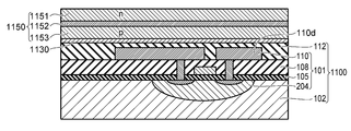
- FIG. 1 is a schematic cross-sectional view illustrating a part of the image display device according to the embodiment.
- FIG. 1 schematically shows the configuration of the sub-pixel 20 of the image display device of the present embodiment.
- the pixel 10 constituting the image displayed on the image display device is composed of a plurality of subpixels 20. In the following, it may be described using the three-dimensional coordinate system of XYZ.
- the subpixels 20 are arranged on a two-dimensional plane. Let the two-dimensional plane in which the subpixels 20 are arranged be the XY plane.
- the subpixels 20 are arranged along the X-axis direction and the Y-axis direction.
- the subpixel 20 has a light emitting surface 153S substantially parallel to the XY plane.
- the light emitting surface 153S mainly outputs light in the positive direction of the Z axis orthogonal to the XY plane.
- FIG. 1 schematically shows a cross section when the subpixel 20 is cut along a plane parallel to the XZ plane.
- This cross-sectional view is a cross-sectional view taken along the line AA'in FIG. 4, which will be described later.
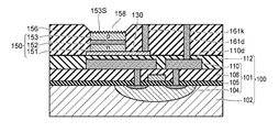
- the subpixel 20 of the image display device includes a transistor 103, a first wiring layer 110, a first interlayer insulating film (first insulating film) 112, and a second wiring layer (first wiring layer). 2 wiring layer) 130, light emitting element 150, second interlayer insulating film (second insulating film) 156, third wiring layer (third wiring layer) 160, via (first via) 161d, To be equipped.
- the subpixel 20 further includes a color filter 180.
- the color filter (wavelength conversion member) 180 is provided on the surface resin layer 170 via a transparent thin film adhesive layer 188.
- the surface resin layer 170 is provided on the light emitting element 150, the interlayer insulating film 156, and the wiring layer 160.
- the transistor 103 is formed on the substrate 102.
- circuit elements such as other transistors and capacitors are formed on the substrate 102, and the circuit 101 is formed by wiring or the like.
- the transistor 103 corresponds to the drive transistor 26 shown in FIG. 3, which will be described later, and the selection transistor 24, the capacitor 28, and the like are other circuit elements.
- the circuit 101 includes an element forming region 104 in which a circuit element is formed, an insulating layer 105, a wiring layer 110, a via connecting the wiring layer 110 and the circuit element, and an insulating film 108 that insulates between the circuit elements. ..
- the circuit board 100 may include other components such as the substrate 102, the circuit 101, and the interlayer insulating film 112.
- the transistor 103 includes a p-type semiconductor region 104b, an n-type semiconductor region 104s and 104d, and a gate 107.
- the gate 107 is provided on the p-type semiconductor region 104b via the insulating layer 105.
- the insulating layer 105 is provided to insulate the element forming region 104 and the gate 107 and to sufficiently insulate the other adjacent circuit elements. When a voltage is applied to the gate 107, a channel can be formed in the p-type semiconductor region 104b.
- the transistor 103 is an n-channel transistor, for example, an n-channel MOSFET.
- the element forming region 104 is provided on the substrate 102.
- the substrate 102 is, for example, a Si substrate.
- the element forming region 104 includes a p-type semiconductor region 104b and n-type semiconductor regions 104s and 104d.
- the p-type semiconductor region 104b is provided near the surface of the substrate 102.
- the n-type semiconductor regions 104s and 104d are provided in the p-type semiconductor region 104b in the vicinity of the surface of the p-type semiconductor region 104b so as to be separated from each other.
- An insulating layer 105 is provided on the surface of the substrate 102.
- the insulating layer 105 also covers the element forming region 104, and also covers the surfaces of the p-type semiconductor region 104b and the n-type semiconductor regions 104s and 104d.
- the insulating layer 105 is, for example, SiO 2 .
- the insulating layer 105 may be a multi-layered insulating layer containing SiO 2 or Si 3 N 4 depending on the covering region.
- the insulating layer 105 may include a layer of an insulating material having a high dielectric constant.
- a gate 107 is provided on the p-type semiconductor region 104b via the insulating layer 105.
- the gate 107 is provided between the n-type semiconductor regions 104s and 104d.
- the gate 107 is, for example, polycrystalline Si.
- the gate 107 may contain silicide or the like having a resistance lower than that of polycrystalline Si.
- the gate 107 and the insulating layer 105 are covered with the insulating film 108.
- the insulating film 108 is, for example, SiO 2 or Si 3 N 4 or the like.
- an organic insulating film such as PSG (Phosphorus Silicon Glass) or BPSG (Boron Phosphorus Silicon Glass) may be further provided.
- a first wiring layer (first wiring layer) 110 is formed on the insulating film 108.
- the first wiring layer 110 includes a plurality of wirings having different potentials, and includes wirings 110s and 110d. As described above, in the cross-sectional views after FIG. 1, the wiring layer is assumed to display a code at a position next to one wiring included in the wiring layer.
- Vias 111s and 111d are provided between the wirings 110s and 110d of the wiring layer 110 and the n-type semiconductor regions 104s and 104d, respectively, and are electrically connected to each other.
- the wiring layer 110 and the vias 111s and 111d are formed of, for example, a metal such as Al or Cu.
- the wiring layer 110 and the vias 111s and 111d may contain a refractory metal or the like.
- a first interlayer insulating film 112 is further provided as a flattening film on the insulating film 108 and the wiring layer 110.
- the interlayer insulating film (first insulating film) 112 is, for example, an organic insulating film such as PSG or BPSG.
- the first interlayer insulating film 112 also functions as a protective film that protects the surface of the circuit board 100.
- the second wiring layer 130 is provided on the interlayer insulating film 112.
- the wiring layer 130 includes a light-shielding plate (part) 130a.
- the light-shielding plate 130a is provided for each subpixel, and the plurality of light-shielding plates 130a are electrically insulated from each other.
- Light emitting elements 150 are provided on the light-shielding plate 130a, respectively.
- the wiring layer 130 that is, the light-shielding plate 130a is made of a material having high conductivity.
- the light-shielding plate 130a contains, for example, Ti, Al, an alloy of Ti and Sn, and the like. It may contain a noble metal having high light reflectivity such as Cu and V, or Ag and Pt. Since the light-shielding plate 130a is made of such a metal material having high conductivity, the light emitting element 150 and the circuit 101 are electrically connected with low resistance.
- the outer circumference of the light-shielding plate 130a includes the outer circumference when the light emitting element 150 is projected from above the Z axis in the XY plan view.
- the light-shielding plate 130a can reflect the scattering of light downward from the light-emitting element 150 toward the light-emitting surface 153S so that it does not reach the transistor 103.
- the material of the light-shielding plate 130a it is possible to improve the luminous efficiency by reflecting the scattering of light downward of the light emitting element 150 toward the light emitting surface 153S side.
- the light-shielding plate 130a blocks the scattered light below the light emitting element 150, the arrival of the light to the transistor 103 is suppressed, and the malfunction of the transistor 103 can be prevented.
- the light emitting element 150 includes an n-type semiconductor layer (first semiconductor layer) 151, a light emitting layer 152, and a p-type semiconductor layer (second semiconductor layer) 153.
- the n-type semiconductor layer 151, the light emitting layer 152, and the p-type semiconductor layer 153 are laminated in this order from the interlayer insulating film 112 in the positive direction of the Z axis. That is, each layer of the light emitting element 150 is laminated from the interlayer insulating film 112 toward the light emitting surface 153S.
- the light emitting element 150 has, for example, a substantially square or rectangular shape in an XY plan view, but the corners may be rounded.
- the light emitting element 150 may have, for example, an elliptical shape or a circular shape in an XY plan view. The degree of freedom in layout is improved by appropriately selecting the shape and arrangement of the light emitting elements in a plan view.
- the light emitting element 150 for example, a nitride semiconductor such as In X Al Y Ga 1-XY N (0 ⁇ X, 0 ⁇ Y, X + Y ⁇ 1) is preferably used.
- the light emitting element 150 in one embodiment of the present invention is a so-called blue light emitting diode, and the wavelength of the light emitted by the light emitting element 150 is, for example, about 467 nm ⁇ 20 nm.
- the wavelength of the light emitted by the light emitting element 150 may be bluish purple emission of about 410 nm ⁇ 20 nm.
- the wavelength of the light emitted by the light emitting element 150 is not limited to the above-mentioned value, and may be appropriate.
- the second interlayer insulating film (second insulating film) 156 covers the first interlayer insulating film 112, the second wiring layer 130, and the light emitting element 150.
- the second interlayer insulating film 156 is preferably formed of a white resin.
- the interlayer insulating film 156 as a white resin, the light emitting element 150 can reflect the light emitted in the lateral direction or the downward direction, and the brightness of the light emitting element 150 can be substantially improved.
- the interlayer insulating film 156 also has a function of protecting the light emitting element 150 and flattening the surface due to the wiring layer 160 formed on the second interlayer insulating film 156.
- the second interlayer insulating film 156 may be a black resin.
- the interlayer insulating film 156 as a black resin, scattering of light in the subpixels is suppressed, and stray light is suppressed more effectively.
- An image display device in which stray light is suppressed can display a sharper image.
- the second interlayer insulating film 156 has an opening 158.
- the opening 158 is formed by removing a part of the interlayer insulating film 156 above the light emitting element 150.
- the opening 158 is formed so that the light emitting surface 153S is exposed from the interlayer insulating film 156.
- the light emitting surface 153S is a surface of the p-type semiconductor layer 153 facing the surface in contact with the light emitting layer 152.
- the light emitting surface 153S is preferably roughened. When the light emitting surface 153S is a rough surface, the light emitting element 150 can improve the light extraction efficiency.
- Via 161k (second via) is provided so as to penetrate the second interlayer insulating film 156. One end of the via 161k is connected to the shading plate 130a.
- the via 161d (first via) is provided so as to penetrate the interlayer insulating films 112 and 156. One end of the via 161d is connected to the wiring 110d.
- the wiring layer 160 is provided on the interlayer insulating film 156.
- the wiring layer 160 includes wirings 160a and 160k. Although not shown in this figure, the wiring 160a is connected to a power line that supplies power to the subpixel 20.
- the wiring 160k is connected to the other ends of the vias 161k and 161d. Therefore, the n-type semiconductor layer 151 of the light emitting element 150 is electrically connected to the drain electrode, which is the main electrode of the transistor 103, via the light-shielding plate 130a, the via 161k, the wiring 160k, the via 161d, and the wiring 110d.
- the transparent electrodes 159a and 159k are provided on the wirings 160a and 160k, respectively.
- the transparent electrode 159a is provided over the light emitting surface 153S of the opened p-type semiconductor layer 153.
- the transparent electrode 159a is provided between the wiring 160a and the light emitting surface 153S, and electrically connects the wiring 160a and the p-type semiconductor layer 153.
- the surface resin layer 170 covers the transparent conductive film including the second interlayer insulating film 156, the transparent electrodes 159a and 159k, and the third wiring layer 160.
- the surface resin layer 170 is a transparent resin, which protects the interlayer insulating film 156 and the wiring layer 160, and provides a flattening surface for adhering the color filter 180.
- the color filter 180 includes a light-shielding unit 181 and a color conversion unit 182.
- the color conversion unit 182 is provided directly above the light emitting surface 153S of the light emitting element 150 according to the shape of the light emitting surface 153S.
- the portion other than the color conversion unit 182 is a light-shielding unit 181.
- the light-shielding unit 181 is a so-called black matrix, which reduces bleeding due to color mixing of light emitted from the adjacent color conversion unit 182 and makes it possible to display a sharp image.
- the color conversion unit 182 has one layer or two layers.
- FIG. 1 shows a two-layer portion. Whether it is one layer or two layers is determined by the color of the light emitted by the subpixel 20, that is, the wavelength.
- the color conversion unit 182 preferably has two layers.
- the emission color of the subpixel 20 is blue, it is preferably one layer.
- the first layer closer to the light emitting element 150 is the color conversion layer 183
- the second layer is the filter layer 184. That is, the filter layer 184 is laminated on the color conversion layer 183.
- the color conversion layer 183 is a layer that converts the wavelength of the light emitted by the light emitting element 150 into a desired wavelength.
- the light having a wavelength of 467 nm ⁇ 20 nm of the light emitting element 150 is converted into light having a wavelength of, for example, about 630 nm ⁇ 20 nm.
- the light having a wavelength of 467 nm ⁇ 20 nm of the light emitting element 150 is converted into light having a wavelength of, for example, about 532 nm ⁇ 20 nm.
- the filter layer 184 blocks the wavelength component of blue light emission remaining without color conversion in the color conversion layer 183.
- the subpixel 20 may output the light through the color conversion layer 183, or the subpixel 20 outputs the light as it is without passing through the color conversion layer 183. You may do so.
- the wavelength of the light emitted by the light emitting element 150 is about 467 nm ⁇ 20 nm
- the subpixel 20 may output the light without passing through the color conversion layer 183.
- the wavelength of the light emitted by the light emitting element 150 is 410 nm ⁇ 20 nm, it is preferable to provide one color conversion layer 183 in order to convert the wavelength of the output light to about 467 nm ⁇ 20 nm.
- the subpixel 20 may have a filter layer 184.
- the filter layer 184 By providing the filter layer 184 on the blue subpixel 20, minute external light reflection generated on the surface of the light emitting element 150 is suppressed.
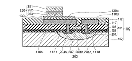
- FIGS. 2A and 2B are schematic cross-sectional views illustrating a modified example of the image display device of the present embodiment, respectively.
- the display of the surface resin layer 170 and the color filter 180 is omitted in order to avoid complication.
- a surface resin layer 170 and a color filter 180 are provided on the second interlayer insulating film and the third wiring layer. The same applies to the cases of other embodiments and modifications thereof described later.
- the wiring structure of the subpixel 20a connected to the light emitting element 150 is different from that of the above-described first embodiment.
- the other components are the same as those in the first embodiment described above, and detailed description thereof will be omitted as appropriate.
- the subpixel 20a includes the wiring 160a1.
- the wiring 160a1 is formed as wiring included in the third wiring layer 160.
- the electrical connection with the p-type semiconductor layer 153 is performed by connecting one end of the wiring 160a1 to a part of the light emitting surface 153S.
- the step of forming the transparent conductive film including the transparent electrode can be omitted.
- the second interlayer insulating film 156a is a transparent resin.
- the interlayer insulating film 156a is not provided with an opening corresponding to the light emitting surface 153S.
- the light emitting surface 153S is directly connected to the wiring 160a2 of the third wiring layer 160.
- the light emitting element 150 emits light from the light emitting surface 153S via the interlayer insulating film 156a.
- the step of forming an opening in the interlayer insulating film 156a and the step of roughening the light emitting surface 153S can be omitted.
- any of the configurations of the subpixels 20, 20a, and 20b shown above can be included. Further, as in the case of the present embodiment, the modification of the subpixel can be applied to each of the embodiments described below.
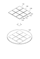
- FIG. 3 is a schematic block diagram illustrating an image display device according to the present embodiment.
- the image display device 1 of the present embodiment includes a display area 2.
- Subpixels 20 are arranged in the display area 2.
- the subpixels 20 are arranged in a grid pattern, for example. For example, n subpixels 20 are arranged along the X axis, and m subpixels 20 are arranged along the Y axis.
- Pixel 10 includes a plurality of subpixels 20 that emit light of different colors.
- the subpixel 20R emits red light.
- the subpixel 20G emits green light.
- the subpixel 20B emits blue light.
- the emission color and brightness of one pixel 10 are determined by the three types of sub-pixels 20R, 20G, and 20B emitting light with desired brightness.
- One pixel 10 includes three sub-pixels 20R, 20G, 20B, and the sub-pixels 20R, 20G, 20B are linearly arranged on the X-axis, for example, as in this example.
- subpixels of the same color may be arranged in the same column, or subpixels of different colors may be arranged for each column as in this example.
- the image display device 1 further includes a power supply line 3 and a ground line 4.
- the power line 3 and the ground line 4 are arranged in a grid pattern along the array of subpixels 20.
- the power supply line 3 and the ground line 4 are electrically connected to each subpixel 20, and power is supplied to each subpixel 20 from a DC power source connected between the power terminal 3a and the GND terminal 4a.
- the power supply terminal 3a and the GND terminal 4a are provided at the ends of the power supply line 3 and the ground line 4, respectively, and are connected to a DC power supply circuit provided outside the display area 2. A positive voltage is supplied to the power supply terminal 3a with reference to the GND terminal 4a.
- the image display device 1 further has a scanning line 6 and a signal line 8.
- the scanning line 6 is laid out in a direction parallel to the X axis. That is, the scanning lines 6 are laid out along the array in the row direction of the subpixels 20.
- the signal line 8 is laid out in a direction parallel to the Y axis. That is, the signal line 8 is laid out along the array of the subpixels 20 in the column direction.
- the image display device 1 further includes a row selection circuit 5 and a signal voltage output circuit 7.
- the row selection circuit 5 and the signal voltage output circuit 7 are provided along the outer edge of the display area 2.
- the row selection circuit 5 is provided along the Y-axis direction of the outer edge of the display area 2.
- the row selection circuit 5 is electrically connected to the subpixels 20 of each column via the scanning line 6 to supply a selection signal to each subpixel 20.
- the signal voltage output circuit 7 is provided along the outer edge of the display area 2.
- the signal voltage output circuit 7 is provided along the X-axis direction of the outer edge of the display area 2.
- the signal voltage output circuit 7 is electrically connected to the subpixel 20 of each line via the signal line 8 to supply a signal voltage to each subpixel 20.
- the subpixel 20 includes a light emitting element 22, a selection transistor 24, a drive transistor 26, and a capacitor 28.
- the selection transistor 24 may be displayed as T1
- the drive transistor 26 may be displayed as T2
- the capacitor 28 may be displayed as Cm.
- the light emitting element 22 is connected in series with the drive transistor 26.
- the drive transistor 26 is an n-channel MOSFET, and the cathode electrode, which is the n electrode of the light emitting element 22, is connected to the drain electrode, which is the main electrode of the drive transistor 26.
- the series circuit of the light emitting element 22 and the drive transistor 26 is connected between the power supply line 3 and the ground line 4.
- the drive transistor 26 corresponds to the transistor 103 in FIG. 1 and the like
- the light emitting element 22 corresponds to the light emitting element 150 in FIG. 1 and the like.
- the voltage applied between the gate and the source of the drive transistor 26 determines the current flowing through the light emitting element 22, and the light emitting element 22 emits light with a brightness corresponding to the current flowing through the light emitting element 22.
- the selection transistor 24 is connected between the gate electrode of the drive transistor 26 and the signal line 8 via a main electrode.
- the gate electrode of the selection transistor 24 is connected to the scanning line 6.
- a capacitor 28 is connected between the gate electrode of the drive transistor 26 and the ground wire 4.
- the row selection circuit 5 selects one row from the array of subpixels 20 in the m row and supplies the selection signal to the scanning line 6.
- the signal voltage output circuit 7 supplies a signal voltage having the required analog voltage value for each subpixel 20 in the selected row.
- a signal voltage is applied between the gate and source of the drive transistor 26 of the subpixel 20 in the selected row.
- the signal voltage is held by the capacitor 28.
- the drive transistor 26 causes a current corresponding to the signal voltage to flow through the light emitting element 22.
- the light emitting element 22 emits light with a brightness corresponding to the flowing current.
- the row selection circuit 5 sequentially switches the rows to be selected and supplies the selection signal. That is, the row selection circuit 5 scans the row in which the subpixels 20 are arranged. A current corresponding to the signal voltage flows through the light emitting element 22 of the subpixel 20 that is sequentially scanned to emit light. Each pixel 10 emits light with an emission color and brightness determined by the emission color and brightness of each RGB color sub-pixel 20, and an image is displayed in the display area 2.
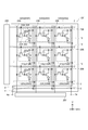
- FIG. 4 is a schematic plan view illustrating a part of the image display device of the present embodiment.
- the light emitting element 22 (150) and the drive transistor 26 (103) are laminated in the Z-axis direction, and the cathode electrode of the light emitting element 22 (150) is formed by the via 161d. Is electrically connected to the drain electrode of the drive transistor 26 (103).
- the plan view of the I layer is schematically displayed in the upper part of FIG. 4, and the plan view of the II layer is schematically displayed in the lower part.
- the first layer is referred to as “I” and the second layer is referred to as “II”.
- the I-th layer is a layer on which the light emitting element 22 (150) is formed. That is, in FIG. 1, the first layer includes layers from the second wiring layer 130 to the third wiring layer 160 in the positive direction of the Z axis.
- the second interlayer insulating film 156 is not shown.
- the second layer includes the layers from the substrate 102 to the first interlayer insulating film 112 in the positive direction of the Z axis in FIG.
- the substrate 102, the insulating layer 105, the insulating film 108, and the first interlayer insulating film 112 are not shown.
- the channel region 104c is shown as the element forming region 104.
- the cross-sectional view shown in FIG. 1 is a cross-sectional view taken along the line AA'at the location indicated by the alternate long and short dash line in each of the I layer and the II layer.
- the n-type semiconductor layer 151 which is the cathode electrode of the light emitting element 150, is connected to the wiring 160k via the via 161k shown in FIG. 1 and its contact hole 161k1.
- the wiring 160k is connected to one end of the via 161d via a contact hole 161d1 provided in the second interlayer insulating film 156.
- the via 161d is schematically shown by a chain double-dashed line in the figure.
- a transparent electrode 159k is provided on the wiring 160k.
- the p-type semiconductor layer 153 which is the anode electrode of the light emitting element 150, is provided with a transparent electrode 159a over the entire surface of the light emitting surface 153S.
- the transparent electrode 159a is also provided on the wiring 160a, which is the third wiring layer 160.
- the transparent electrode 159a is provided between the light emitting surface 153S and the wiring 160a which is the third wiring layer 160, and electrically connects them.
- the other end of the via 161d is connected to the wiring 110d via the contact hole 161d2 provided in the first interlayer insulating film 112.
- the wiring 110d is connected to the via 111d (FIG. 1) via the contact hole 111c1 opened in the insulating film 108, and is connected to the drain electrode of the transistor 103.
- the light emitting element 150 and the transistor 103 formed in the first layer and the second layer, which are different layers, can be electrically connected by the via 161d penetrating the interlayer insulating films 156 and 112.
- the arrangement in which the light emitting element 150 is shielded from light emission by the light shielding plate 130a will be described with reference to FIG.
- the light emitting element 150 has a rectangular bottom surface having a length L1 in the X-axis direction and a length W1 in the Y-axis direction.
- the light-shielding plate (part) 130a has a rectangular shape having a length L2 in the X-axis direction and a length W2 in the Y-axis direction.
- the light emitting element 150 is provided on the light shielding plate 130a.
- the length of each part described above is set so that L2> L1 and W2> W1.
- the light emitting element 150 is provided on the light emitting plate 130a, and the outer periphery of the light emitting plate 130a is arranged so as to include the outer periphery of the light emitting element 150.
- the outer circumference of the light-shielding plate 130a may include the outer circumference of the light-emitting element 150, and the shape of the light-shielding plate 130a and the shape of the light-emitting element 150 are not limited to a square shape and may be any suitable shape.
- the light emitting element 150 emits light upward, and also emits light downward, and includes reflected light, scattered light, and the like at the interface between the interlayer insulating film 112 and the surface resin layer 170. Therefore, preferably, the outer circumference of the light-shielding plate 130a is set to include the outer circumference of the light emitting element 150 projected on the light-shielding plate 130a in XY plan view. By setting the light-shielding plate 130a in this way, it is possible to suppress the arrival of light below the light emitting element 150 and reduce the influence of light on the circuit element.
- the manufacturing method of the image display device 1 of this embodiment will be described.
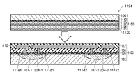
- 5A to 9B are schematic cross-sectional views illustrating the method of manufacturing the image display device of the present embodiment.
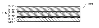
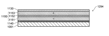
- the semiconductor growth substrate 1194 is prepared.
- the semiconductor growth substrate 1194 has a semiconductor layer 1150 grown on the crystal growth substrate (first substrate) 1001.
- the crystal growth substrate 1001 is, for example, a Si substrate, a sapphire substrate, or the like.
- a Si substrate is used.
- the buffer layer 1140 is formed on one surface of the crystal growth substrate 1001.
- nitride such as AlN is preferably used as the buffer layer (buffer layer) 1140.
- the buffer layer 1140 is used to alleviate the mismatch at the interface between the GaN crystal and the crystal growth substrate 1001 when epitaxially growing GaN.
- the p-type semiconductor layer 1153, the light emitting layer 1152, and the n-type semiconductor layer 1151 are laminated on the buffer layer 1140 in this order from the buffer layer 1140 side.
- a vapor phase growth method (Chemical Vapor Deposition, CVD method) is used, and an organic metal vapor deposition method (Metal Organic Chemical Vapor Deposition, MOCVD method) is preferably used.
- the semiconductor layer 1150 is, for example, In X Al Y Ga 1-XY N (0 ⁇ X, 0 ⁇ Y, X + Y ⁇ 1) or the like.
- a metal layer 1130 is formed on the surface of the semiconductor layer 1150 facing the surface of the crystal growth substrate 1001. That is, the metal layer 1130 is formed on the surface of the n-type semiconductor layer 1151 facing the surface of the n-type semiconductor layer 1151 provided with the light emitting layer 152.
- the metal layer 1130 includes, for example, Ti, Al, an alloy of Ti and Sn, and the like. It may contain a noble metal having high light reflectivity such as Cu and V, or Ag and Pt.
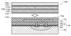
- the circuit board 1100 is prepared.
- the circuit board (second board) 1100 includes the circuit 101 described with reference to FIG. 1 and the like.
- the semiconductor growth substrate 1194 is turned upside down. That is, as shown by the arrows in the figure, one surface of the circuit board 1100 faces the surface of the metal layer 1130 formed on the semiconductor layer 1150, and both are bonded to each other.
- the bonded surface of the circuit board 1100 is an exposed surface of the interlayer insulating film 112 formed on the wiring layer 110.
- the crystal growth substrate 1001 is removed. For removing the crystal growth substrate 1001, for example, wet etching or laser lift-off is used.
- a low melting point metal or a low melting point alloy may be used for heat crimping.
- the low melting point metal is, for example, Sn, In, or the like, and the low melting point alloy can be, for example, an alloy containing Zn, In, Ga, Sn, Bi, or the like as a main component.
- the bonded surfaces of each substrate are flattened using chemical mechanical polishing (CMP), etc., and then the bonded surfaces are cleaned and adhered in vacuum by plasma treatment. You may let it.
- CMP chemical mechanical polishing
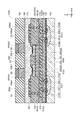
- FIGS. 6A to 6C show examples of modifications in the wafer bonding process.
- any of FIGS. 6A to 6C can be used instead of the step of FIG. 5B.
- the semiconductor layer 1150 is grown and laminated on the crystal growth substrate 1001 in the order of the n-type semiconductor layer 1151, the light emitting layer 1152, and the p-type semiconductor layer 1153 from the side of the crystal growth substrate 1001.
- the support substrate 1190 is adhered to the surface of the p-type semiconductor layer 1153 facing the surface on which the light emitting layer 1152 is provided, that is, the open surface of the p-type semiconductor layer 1153.
- the support substrate 1190 (third substrate) is formed of, for example, Si or quartz.
- the crystal growth substrate 1001 is removed.
- a laser is used to remove the crystal growth substrate 1001.
- the metal layer 1130 is formed on the open surface of the n-type semiconductor layer 1151.
- the support substrate 1190 is adhered after removing the buffer layer 1140, but the support substrate 1190 may be adhered to the buffer layer 1140 and the buffer layer 1140 may be removed after the wafer bonding step.
- the metal layer 1130 may be formed on the semiconductor growth substrate 1194, and the metal layer 1120 may be formed on the circuit board 1100 as well.
- wafer bonding can be performed more easily by using the same metal material in each metal layer or by using an alloy containing the same metal material.
- the metal layer may be provided on at least one of the semiconductor growth substrate 1194 side and the circuit board 1100 side.
- the semiconductor growth substrate when the semiconductor layer 1150 is crystal-grown on the crystal growth substrate 1001, the semiconductor growth substrate may be formed without passing through the buffer layer 1140. In this case, the step of removing the buffer layer after wafer bonding can be omitted.
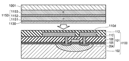
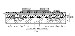
- the circuit board 1100 is bonded to the semiconductor layer 1150 via the metal layer 1130 by wafer bonding.
- the metal layer 1130 and the semiconductor layer 1150 are formed into a required shape by etching.
- the metal layer 1130 is etched to form a second wiring layer 130.
- the wiring layer 130 includes a light-shielding plate 130a.
- the light-shielding plate 130a is formed into the above-mentioned shape by etching.
- the semiconductor layer 1150 is further etched and formed into the shape of the light emitting element 150.
- a dry etching process is used, and preferably anisotropic plasma etching (Reactive Ion Etching, RIE) is used.
- an interlayer insulating film 156 is formed so as to cover the light emitting element 150. Via holes are formed in the interlayer insulating film 156. After that, the via hole is filled with a conductive metal material. Either wet etching or dry etching can be used to form the via holes.
- a conductive layer is formed in the via hole by sputtering or the like. After forming the via hole, the via and the wiring layer may be formed at the same time.
- An opening 158 is formed by etching the second interlayer insulating film 156 to expose the surface of the p-type semiconductor layer 153.
- the etching may be wet etching or dry etching.
- the light emitting surface 153S of the exposed p-type semiconductor layer 153 is roughened by wet etching or the like in order to improve the luminous efficiency.
- a third wiring layer 160 including the opening 158 is formed, and the wirings 160a and 160k are formed by photolithography.
- the wiring 160a is not connected to the p-type semiconductor layer 153.
- a transparent conductive film covering the wiring layer 160, the second interlayer insulating film 156, and the light emitting surface 153S of the p-type semiconductor layer 153 is formed.
- the transparent conductive film an ITO film, a ZnO film, or the like is preferably used.
- the required transparent electrodes 159a, 159k are formed by photolithography.
- the transparent electrode 159a is formed not only on the wiring 160a but also on the light emitting surface 153S of the p-type semiconductor layer 153. Therefore, the wiring 160a and the p-type semiconductor layer 153 are electrically connected.
- the transparent electrode 159a is provided so as to cover the entire surface of the exposed light emitting surface 153S and is connected to the light emitting surface 153S.
- FIG. 9A and 9B show the manufacturing process corresponding to the subpixels 20a and 20b of the modified example, respectively.
- FIG. 9A is executed after the step of FIG. 7B to form the subpixel 20a.
- FIG. 9B is executed after the step of FIG. 7B to form the subpixel 20b.
- each wiring 160a1, 160k is formed.
- the wiring 160a1 is connected to the light emitting surface 153S of the p-type semiconductor layer 153 instead of the electrical connection by the transparent electrode.
- the third wiring layer 160 is formed without forming an opening, and the wiring is formed on the light emitting surface 153S of the p-type semiconductor layer 153. It is connected by 160a2.
- the circuit board 1100 is a wafer containing the circuit 101.
- Circuit boards 1100 are formed with circuits 101 for one or more image display devices.
- the circuit 101 for forming one image display device is divided into a plurality of circuit boards 1100 and formed, and all of the divided circuits are combined to form 1 One image display device may be configured.
- the crystal growth substrate 1001 is a wafer having the same size as the wafer-shaped circuit board 1100.
- FIG. 10 is a perspective view illustrating a method of manufacturing the image display device of the present embodiment. As shown in FIG. 10, a plurality of semiconductor growth substrates 1194 may be prepared, and the semiconductor layers 1150 formed on the plurality of crystal growth substrates 1001 may be bonded to one circuit board 1100.
- a plurality of circuits 101 are arranged in a grid pattern on the circuit board 1100, for example.
- the circuit 101 includes all the subpixels 20 and the like required for one image display device 1.
- the circuits 101 arranged adjacent to each other are provided with an interval of about the width of the scribe line. No circuit element or the like is arranged at or near the end of the circuit 101.
- the crystal quality tends to deteriorate at the end of the semiconductor layer 1150 and its vicinity. Therefore, by matching the end portion of the semiconductor layer 1150 with the end portion of the circuit 101, a region in the vicinity of the end portion of the semiconductor layer 1150 on the semiconductor growth substrate 1194 where the crystal quality is likely to deteriorate is a display region of the image display device 1. Can be avoided.
- a plurality of circuit boards 1100 are prepared, and the plurality of circuit boards 1100 are bonded to the semiconductor layer 1150 formed on the crystal growth substrate 1001 of one semiconductor growth substrate 1194. You may.
- FIG. 11 is a schematic cross-sectional view illustrating the method for manufacturing the image display device of the present embodiment.
- the wiring and the like in the circuit board 100 and the interlayer insulating films 112 and 156 are not shown. Further, in FIG. 11, a part of the color conversion member such as the color filter 180 is displayed.
- the structure including the wiring layer 130, the light emitting element 150, vias 161k, 161d, the wiring layer 160, the interlayer insulating film 156, and the surface resin layer 170 is referred to as a light emitting circuit unit 172. Further, a structure in which the light emitting circuit unit 172 is provided on the circuit board 100 is referred to as a structure 1192.
- the color filter 180 is adhered to the structure 1192 on one side.
- the other surface of the color filter 180 is adhered to the glass substrate 186.
- a transparent thin film adhesive layer 188 is provided on one surface of the color filter 180, and is adhered to the surface of the structure 1192 on the light emitting circuit portion 172 side via the transparent thin film adhesive layer 188.
- the color filter 180 has color conversion units arranged in the positive direction of the X-axis in the order of red, green, and blue.
- a red color conversion layer 183R and a green color conversion layer 183G are provided on the first layer, and a filter layer 184 is provided on the second layer, respectively.
- a single-layer color conversion layer 183B is provided for blue.
- a light-shielding unit 181 is provided between the color conversion units.
- the color filter 180 is attached to the structure 1192 by aligning the positions of the color conversion layers 183R, 183G, and 183B of each color with the positions of the light emitting element 150.
- 12A to 12D are schematic cross-sectional views showing a modified example of the manufacturing method of the image display device of the present embodiment.
- 12A-12D show a method of forming a color filter by an inkjet.
- a structure 1192 having a light emitting circuit unit 172 attached to the circuit board 100 is prepared.
- a light-shielding portion 181a is formed on the structure 1192.
- the light-shielding portion 181a is formed by using, for example, screen printing, photolithography technology, or the like.
- the phosphor 183a corresponding to the emission color is ejected from the inkjet nozzle.
- the phosphor 183a colors the region where the light-shielding portion 181a is not formed.
- a fluorescent paint using a general phosphor material or a quantum dot phosphor material is used as the phosphor 183a.
- a quantum dot phosphor material it is preferable because each emission color can be realized, monochromaticity is high, and color reproducibility can be high.
- a drying process is performed at an appropriate temperature and time. The thickness of the coating film at the time of coloring is set to be thinner than the thickness of the light-shielding portion 181a.
- the blue light emitting subpixel may not form a color conversion part, so that the phosphor is not ejected.
- the color conversion unit may be one layer, so that the thickness of the coating film of the blue phosphor is preferably set to that of the light shielding portion 181a. It is about the same as the thickness.
- the paint 184a for the filter layer is ejected from the inkjet nozzle.
- the paint 184a is applied over the coating film of the phosphor 183a.
- the total thickness of the coating film of the phosphor 183a and the coating film 184a is about the same as the thickness of the light-shielding portion 181a.
- the image display device 1 can be manufactured.
- the semiconductor layer 1150 including the light emitting layer 1152 for the light emitting element 150 is mounted on the circuit board 1100 (100) including the circuit elements such as the transistor 103 for driving the light emitting element 150. to paste together. After that, the semiconductor layer 1150 is etched to form the light emitting element 150. Therefore, the step of transferring the light emitting element can be remarkably shortened as compared with the case of individually transferring the light emitting element separated into the circuit board 1100 (100).
- the number of subpixels exceeds 24 million, and in the case of an 8K image quality image display device, the number of subpixels exceeds 99 million. It would take an enormous amount of time to mount such a large number of light emitting elements individually on a circuit board, and it is difficult to realize an image display device using micro LEDs at a realistic cost. Further, if a large number of light emitting elements are individually mounted, the yield is reduced due to poor connection at the time of mounting, and further cost increase is unavoidable.
- the entire semiconductor layer 1150 is attached to the circuit board 1100 (100) before the semiconductor layer 1150 is fragmented, so that the transfer step is performed once. Complete with.
- the light emitting element is directly formed on the circuit board by etching or the like, the light emitting element and the circuit element in the circuit board 1100 (100) are electrically connected by via formation, so that a uniform connection structure is realized. It is possible to suppress a decrease in yield.
- the semiconductor layer 1150 is attached to the circuit board 1100 (100) at the wafer level without being fragmented in advance or forming an electrode at a position corresponding to the circuit element, there is no need to perform alignment. Therefore, the pasting process can be easily performed in a short time. Since it is not necessary to align the light emitting element 150 at the time of pasting, the light emitting element 150 can be easily miniaturized, which is suitable for a high-definition display.
- the metal layers 1130 and 1120 are formed in advance on at least one of the bonded surfaces of the semiconductor layer 1150 and the circuit board 1100. Therefore, wafer bonding can be easily performed by appropriately selecting the material of the metal layer.
- the metal layer formed during wafer bonding can be used as the second wiring layer 130 for connecting the light emitting element 150 to the outside or the like.
- the via 161k and the n-type semiconductor layer 151 can be electrically connected with a low resistance value.
- the second wiring layer 130 can include the light-shielding plate 130a, it is possible to prevent the circuit elements such as the transistor 103 from malfunctioning due to unnecessary light scattering of the light emitting element 150.
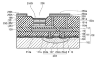
- FIG. 13 is a schematic cross-sectional view illustrating a part of the image display device according to the present embodiment.
- FIG. 13 schematically shows a cross section when the subpixel 220 is cut along a plane parallel to the XZ plane.
- This cross-sectional view is a cross-sectional view corresponding to the cross-sectional view taken along the line AA'of FIG. 4 described above.
- the configuration of the light emitting element 250 and the configuration of the transistor 203 for driving the light emitting element 250 are different from those of the other embodiments described above.
- the same components as those in the other embodiments described above are designated by the same reference numerals, and detailed description thereof will be omitted as appropriate.
- the subpixel 220 of the image display device of the present embodiment includes the transistor 203 and the light emitting element 250.
- the transistor 203 is formed in the element forming region 204 formed on the substrate 102.
- the element forming region 204 includes an n-type semiconductor region 204b and a p-type semiconductor region 204s and 204d.
- the n-type semiconductor region 204b is provided near the surface of the substrate 102.
- the p-type semiconductor regions 204s and 204d are provided in the n-type semiconductor region 204b in the vicinity of the surface of the n-type semiconductor region 204b so as to be separated from each other.
- a gate 107 is provided on the n-type semiconductor region 204b via the insulating layer 105.
- the gate 107 is provided between the p-type semiconductor regions 204s and 204d.
- the transistor 203 is a p-channel transistor, for example, a p-channel MOSFET.
- a second wiring layer 130 is formed on the first interlayer insulating film 112, as in the case of the other embodiment described above, and a light-shielding plate 130a which is a part of the wiring layer 130 is provided. ..
- the light emitting element 250 may be made of the same material as in the other embodiments described above.
- the light emitting element 250 emits, for example, blue light having a wavelength of about 467 nm ⁇ 20 nm or bluish purple light having a wavelength of 410 nm ⁇ 20 nm.
- the p-type semiconductor layer 253 of the light emitting element 250 is provided on the light-shielding plate 130a.
- the light-shielding plate 130a and the p-type semiconductor layer 253 are ohmic-connected.
- the second interlayer insulating film (second insulating film) 156 covers the first interlayer insulating film 112, the second wiring layer 130, and the light emitting element 250.
- the second interlayer insulating film 156 has an opening 258.
- the opening 258 is formed on the light emitting element 250, and the interlayer insulating film 156 is not provided on the light emitting surface 251S of the light emitting element 250.
- a white resin is preferably used so that the light emitting element 250 reflects the light emitted and is effectively output from the opening 258.
- the light emitting surface 251S is a surface of the n-type semiconductor layer 251 facing the surface in contact with the light emitting layer 252.
- the light emitting surface 251S is roughened.
- a via 261a is provided so as to penetrate the interlayer insulating film 156. One end of the via 261a is connected to the shading plate 130a.
- the via 161d is provided so as to penetrate the interlayer insulating films 112 and 156. One end of the via 161d is connected to the wiring 110d.
- the wiring layer 260 is provided on the interlayer insulating film 156.
- the wiring layer 260 includes wirings 260k and 260a.
- the wiring 260a is connected to the other ends of the vias 261a and 161d. Therefore, the p-type semiconductor layer 253 of the light emitting element 250 is electrically connected to the main electrode of the transistor 203 via the vias 261a and 161d.
- Wiring 260k is not shown, but is connected to the ground wire.
- a transparent electrode 259k is provided on the wiring 260k.
- the transparent electrode 259k extends to the light emitting surface 251S and is provided over the entire surface of the light emitting surface 251S. Therefore, the n-type semiconductor layer 251 is connected to the ground wire via the transparent electrode 259k and the wiring 260k.
- a transparent electrode 259a is also arranged on the wiring 260a.
- a surface resin layer 170 is provided on the interlayer insulating film 156 and the transparent electrodes 259k and 259a.
- FIG. 14 is a schematic block diagram illustrating an image display device according to the present embodiment.
- the image display device 201 of the present embodiment includes a display area 2, a row selection circuit 205, and a signal voltage output circuit 207.
- the display area 2 for example, the sub-pixels 220 are arranged in a grid pattern as in the case of the other embodiments described above.
- the subpixel 220 includes a light emitting element 222, a selection transistor 224, a drive transistor 226, and a capacitor 228.
- the selection transistor 224 may be displayed as T1
- the drive transistor 226 may be displayed as T2
- the capacitor 228 may be displayed as Cm.
- the light emitting element 222 is provided on the ground wire 4 side, and the drive transistor 226 connected in series with the light emitting element 222 is provided on the power supply line 3 side. That is, the drive transistor 226 is connected to the higher potential side than the light emitting element 222.
- the drive transistor 226 is a p-channel MOSFET.
- a selection transistor 224 is connected between the gate electrode of the drive transistor 226 and the signal line 208.
- the capacitor 228 is connected between the gate electrode of the drive transistor 226 and the power supply line 3.
- the row selection circuit 205 and the signal voltage output circuit 207 supply the scanning line 206 and the signal line 208 with a signal voltage having a polarity different from that of the other embodiments described above in order to drive the drive transistor 226 which is a p-channel MOSFET. ..
- the row selection circuit 205 supplies a selection signal to the scanning line 206 so as to sequentially select one row from the array of subpixels 220 in the m row.
- the signal voltage output circuit 207 supplies a signal voltage having the required analog voltage value to each subpixel 220 in the selected row.
- the drive transistor 226 of the subpixel 220 in the selected row causes a current corresponding to the signal voltage to flow through the light emitting element 222.
- the light emitting element 222 emits light with a brightness corresponding to the flowing current.
- a method of manufacturing the image display device 201 of the present embodiment will be described.
- 15A to 16C are schematic cross-sectional views illustrating the method of manufacturing the image display device of the present embodiment.
- a semiconductor growth substrate 1294 different from the semiconductor growth substrate 1194 already described in FIG. 5A is prepared.
- the semiconductor growth substrate 1294 has a semiconductor layer 1150 grown on the crystal growth substrate 1001.
- the semiconductor layer 1150 is grown on the crystal growth substrate 1001 via the buffer layer 1140, but the semiconductor layer 1150 may be grown without passing through the buffer layer 1140 in the other embodiments described above. Same as the case.
- the semiconductor growth substrate 1294 is laminated in the order of the n-type semiconductor layer 1151, the light emitting layer 1152, and the p-type semiconductor layer 1153 from the side of the crystal growth substrate 1001.
- the n-type semiconductor layer 1151 in the early stage of crystal growth, crystal defects due to mismatch of crystal lattice constants are likely to occur, and such a crystal exhibits an n-type. Therefore, as in this example, stacking from the n-type semiconductor layer 1151 has an advantage that a large margin in the production process can be obtained and the yield can be easily improved.
- the metal layer 1130 is formed on the side of the p-type semiconductor layer 1153.
- the metal layer By forming the metal layer on the surface of the p-type semiconductor layer 1153, the p-type semiconductor layer 1153 can be protected by the metal layer 1130. Therefore, there is an advantage that the semiconductor growth substrate 1294 can be easily stored.
- a thin film layer using a hole-injectable material at the interface between the p-type semiconductor layer 1153 and the metal layer 1130 it is possible to further reduce the drive voltage of the above-mentioned light emitting element 250. ..
- a hole-injectable material for example, an ITO film or the like can be preferably used.
- the semiconductor growth substrate 1294 is turned upside down and attached to the circuit board 1100. As shown by the arrows in the figure, one surface of the circuit board 1100 and the surface of the metal layer 1130 formed on the semiconductor layer 1150 are aligned and both are attached. The bonded surface of the circuit board 1100 is an exposed surface of the interlayer insulating film 112 formed on the wiring layer 110.
- the wafer bonding described above may be the same as in the case of the modification described in FIGS. 6A to 6C. That is, after transferring the semiconductor layer 1150 to the support substrate, the semiconductor growth substrate may be attached to the circuit board 1100 without being inverted, or the metal layer may be provided on at least one of the semiconductor layer 1150 and the circuit board 1100. Alternatively, the semiconductor layer 1150 in which crystals are grown without passing through the buffer layer 1140 may be attached.
- the circuit board 1100 is bonded to the semiconductor layer 1150 via the metal layer 1130 by wafer bonding. Then, as in the case of the other embodiment described above, the metal layer 1130 forms the second wiring layer 130 and the light-shielding plate 130a, and the semiconductor layer 1150 forms the light emitting element 250.
- An interlayer insulating film 156 is formed so as to cover the light emitting element 250, and a via hole is formed in the interlayer insulating film 156. After that, the via hole is filled with a conductive metal material, a conductive layer is formed in the via hole, and the wiring layer 260 is formed by photolithography.
- An opening 258 is formed in the interlayer insulating film 156, and the light emitting surface 251S is roughened. After that, a third wiring layer 260 including the wirings 260a and 260k is formed, and transparent electrodes 259a and 259k are formed on the third wiring layer 260 by an ITO film or the like.
- This embodiment has the same effect as that of the other embodiments described above. That is, since the semiconductor layer 1150 is bonded to the circuit board 1100 and then the individual light emitting elements 250 are formed by etching, the transfer process of the light emitting elements can be significantly shortened.
- the n-type semiconductor layer 251 as the light emitting surface 251S, the surface can be roughened more easily, and the wiring 260k on the light emitting surface 251S.
- the second wiring layer 130 may be connected to a plurality of different potentials, and the shading plate 130a included in the second wiring layer 130 may be a semiconductor underneath each subpixel. It is connected to the main electrodes of the driving transistors 103 and 203 via vias. Therefore, the shading plate 130a can be set to a different potential for each subpixel.
- the second wiring layer 330 also serves as a light-shielding plate and blocks all light-emitting elements. Further, in the present embodiment, the second wiring layer 330 is connected to a single potential. The wiring layer 330 is connected to the power line in this example.
- FIG. 17 is a schematic cross-sectional view illustrating a part of the image display device according to the present embodiment.
- FIG. 17 schematically shows a cross section when the subpixel 320 is cut along a plane parallel to the XZ plane.
- This cross-sectional view is a cross-sectional view taken along the line BB'of FIG. 18, which will be described later.
- the configuration of the light emitting element 250 is the same as in the case of the second embodiment. That is, the light emitting element 250 has a lower p-type semiconductor layer 253 and an n-type semiconductor layer 251 having a light emitting surface 251S.
- the transistor 103 for driving the light emitting element 250 is an n-channel transistor similar to the case of the first embodiment.
- the same components as those of the other embodiments described above are designated by the same reference numerals, and detailed description thereof will be omitted as appropriate.
- the subpixel 320 of the image display device of the present embodiment includes the transistor 103 and the light emitting element 250.
- the transistor 103 is formed in the element forming region 104 formed on the substrate 102.
- the element forming region 104 includes a p-type semiconductor region 104b and n-type semiconductor regions 104s and 104d, and the transistor 103 is an n-channel transistor.
- the structure of the upper part of the transistor 103 and the wiring structure of the circuit board 100 are the same as those of the first embodiment described above.
- a second wiring layer 330 is formed on the first interlayer insulating film 112.
- the wiring layer 330 is provided so as to substantially cover the circuit element including the transistor 103 provided under each subpixel 320.
- the wiring layer 330 has a through hole 332 for each subpixel 320.
- the second interlayer insulating film 156 is formed on the first interlayer insulating film 112 exposed from the light emitting element 250, the wiring layer 330, and the through hole 332.
- Vias 361k are provided through the interlayer insulating films 156 and 112, and through holes 332 are provided for passing the vias 361k. Since the diameter of the through hole 332 in the XY plan view is set to be larger than the diameter of the via 361k, the via 361k is insulated from the wiring layer 330.
- a transparent electrode 359k is formed over the wiring 360k and the light emitting surface 251S.
- the transparent electrode 359k is provided between the wiring 360k and the light emitting surface 251S, and electrically connects the wiring 360k and the n-type semiconductor layer 251.
- the n-type semiconductor layer 251 of the light emitting element 250 is connected to the drain electrode of the transistor 103 via the transparent electrode 359k, the wiring 360k, the via 361k, and the wiring 110d.
- the p-type semiconductor layer 253 of the light emitting element 250 is provided on the second wiring layer 330.
- the p-type semiconductor layer 253 has an ohmic connection with the wiring layer 330.
- the wiring layer 330 is connected to the power line. Therefore, the p-type semiconductor layer 253 of the light emitting element 250 is connected to the power supply line via the second wiring layer 330.
- FIG. 18 is a schematic plan view illustrating a part of the image display device of the present embodiment.
- the light emitting element is driven by an n-channel transistor.
- the circuit configuration of FIG. 3 is applied to the drive circuit.
- the light emitting element 250 and the driving transistor 103 are laminated in the Z-axis direction, and the via 361k causes the n-type semiconductor layer 251 which is the cathode electrode of the light emitting element 250 and the drain of the transistor 103. It is electrically connected to the electrode.
- the second wiring layer 330 is provided between the light emitting element 250 and the transistor 103.
- the plan view of the Ia layer is schematically displayed in the upper part of FIG. 18, and the plan view of the IIa layer is schematically displayed in the lower part of FIG.
- the layer Ia is referred to as “Ia” and the layer II is referred to as “IIa”.
- the Ia layer is a layer on which the light emitting element 250 is formed.
- the second layer IIa is a layer on which the transistor 103 is formed.
- the second wiring layer 330 is not shown, and the through holes 332 provided in the wiring layer 330 are shown by broken lines in each of the Ia layer and the IIa layer for reference. ..
- the Ia layer includes the p-type semiconductor layer 253 to the transparent electrode 359k in FIG.
- the second interlayer insulating film 156 is not shown.
- the second layer IIa includes layers from the element forming region 104 to the first wiring layer 110.
- the substrate 102, the insulating layer 105, the insulating film 108, and the first interlayer insulating film 112 are not shown.
- the channel region 104c is shown as the element forming region 104 of the driving transistor 103.
- a selection transistor T1 and a capacitor Cm are formed in the other element forming region 104.
- the transparent electrode 359k is provided over the entire surface of the light emitting surface 251S of the light emitting element 250, and is provided on the wiring 360k. Since the transparent electrode 359k is provided between the light emitting surface 251S and the wiring 360k, the light emitting surface 251S, that is, the n-type semiconductor layer 251 and the wiring 360k are electrically connected. The wiring 360k is connected to the via 361k via the contact hole 361k1.
- the via 361k is schematically shown by a chain double-dashed line in the figure.
- the via 361k reaches the contact hole 361k2 through the through hole 332 and is electrically connected to the wiring 110d.
- the wiring 110d is connected to the drain electrode of the transistor 103 via the contact hole 111c on the channel region 104c side.
- the through hole 332 formed in the second wiring layer 330 is opened larger than the cross section of the via 361k.
- a second interlayer insulating film 156 is provided between the wiring layer 330 and the via 361k, and the wiring layer 330 and the via 361k are insulated from each other.
- the n-type semiconductor layer 251 of the light emitting element 250 and the drain electrode of the transistor 103 are electrically connected by the via 361k.
- the second wiring layer 330 is provided over the entire surface of the first interlayer insulating film 112 except for the through hole 332. Further, the through hole 332 is arranged so as to avoid above the circuit element such as the transistor 103. As a result, the wiring layer 330 can reflect the light scattered downward of the light emitting element 250 upward and block the scattering to the circuit element.
- 19A and 19B are schematic cross-sectional views illustrating the method of manufacturing the image display device of the present embodiment.
- the step of bonding the semiconductor layer 1150 and the circuit board 1100 is the same as in the case of the second embodiment described above.
- the steps after the processing up to FIG. 16A will be described.
- the second wiring layer 330 is formed. Etching is used to form the second wiring layer 330.
- the second wiring layer 330 it is formed so as to cover the circuit element on the circuit board 1100 side, and a through hole 332 is formed at a position corresponding to the wiring 110d. Then, it is further etched to form the light emitting element 250.
- a second interlayer insulating film 156 is formed on the light emitting element 250, the second wiring layer 330, and the first interlayer insulating film 112. After that, a via hole is formed in the second interlayer insulating film 156 and filled with a conductive member to form a via 361k.
- An opening 358 is formed in the second interlayer insulating film 156 to expose the light emitting surface 251S.
- a third wiring layer 360 is formed on the interlayer insulating film 156.
- a transparent electrode 359k is formed between the wiring 360k on the cathode electrode side of the wiring layer 360 and the light emitting surface 251S, and the wiring 360k and the n-type semiconductor layer 251 are electrically connected.
- the manufacturing process of the semiconductor layer 1150 described in the first embodiment described above it is possible to obtain a subpixel including the light emitting element 150 and the p-channel transistor 203. That is, by performing the manufacturing steps shown in FIGS. 5A to 6C in the first embodiment, the n-type semiconductor layer 151 is used as the lower layer, the p-type semiconductor layer 153 is used as the light emitting surface 153S, and the p-type semiconductor layer 153 is formed by vias. , Can be connected to the drain electrode of the transistor 203. In this case, the circuit configuration shown in FIG. 13 is obtained, and the second wiring layer is connected to the ground wire.
- the second wiring layer 330 can have a simple pattern of only through holes 332, which facilitates pattern design and makes an image.
- the development period of the display device can be shortened.
- the second wiring layer 330 is assumed to be all connected to the same potential, but may include wiring connected to different potentials.
- the second wiring layers 130, 330 are connected to a single potential for at least one subpixel.
- the second wiring layer can include multiple wires that can be connected to different potentials.
- a light emitting device 250 having an n-type semiconductor layer 251 having a lower p-type semiconductor layer 253 and a light emitting surface 251S will be described, but the lower n-type semiconductor layer 151 and a light emitting surface 153S are provided.
- the case of the light emitting element 150 including the p-type semiconductor layer 153 can also be easily realized by using the steps of the other embodiments described above.
- the light emitting element 250 is driven by the p-channel transistor 203.
- the circuit configuration of FIG. 14 is applied to the drive circuit.
- the circuit of FIG. 3 is applied.
- the via 461d is provided so as to penetrate the interlayer insulating films 156 and 112. One end of the via 461d is connected to the wiring 460a. The other end of the via 461d is connected to the wiring 110d.
- the p-type semiconductor layer 253, which is the anode electrode of the light emitting element 250, is connected to the drain electrode of the transistor 203 of the p channel via the wiring 430a, the via 461a, the wiring 460a, the via 461d, and the wiring 110d.
- the n-type semiconductor layer 251 of the light emitting element 250 has a roughened light emitting surface 251S.
- the transparent electrode 459k is provided over the entire surface on the light emitting surface 251S, and is also provided on the wiring 460k.
- the transparent electrode 459k is provided between the light emitting surface 251S and the wiring 460k, and these are electrically connected to each other.
- a via 461k is provided so as to penetrate the second interlayer insulating film 156.
- One end of the via 461k is connected to the wiring 460k of the third wiring layer 460.
- the other end of the via 461k is connected to the wiring 430k of the second wiring layer 430.
- the wiring 430k is connected to the ground wire 4 (FIG. 13).
- the n-type semiconductor layer 251 which is the cathode electrode of the light emitting element 250 is connected to the ground wire via the transparent electrode 459k, the wiring 460k, the via 461k, and the wiring 430k.
- 21A and 21B are schematic cross-sectional views illustrating the method of manufacturing the image display device of the present embodiment.
- the step of bonding the semiconductor layer 1150 and the circuit board 1100 is the same as in the case of the second embodiment described above.
- the steps after the processing up to FIG. 16A will be described.
- the second wiring layer 430 is formed by etching after forming the light emitting element 250.
- the second wiring layer 430 includes wirings 430a and 430k that are insulated from each other.
- vias 461a and 461k are formed through the interlayer insulating film 156, and vias 461d are formed through the interlayer insulating films 156 and 112.
- a third wiring layer 460 is formed on the interlayer insulating film 156.
- An opening 458 is formed in the second interlayer insulating film 156 at a position corresponding to the light emitting surface 251S.
- transparent electrodes 459a and 459k are formed on the wirings 460a and 460k.
- the transparent electrode 459k is provided over the entire surface of the light emitting surface 251S and is provided between the light emitting surface 251S and the wiring 460k to electrically connect the n-type semiconductor layer 251 and the wiring 460k.
- the second wiring layer includes wirings 460a and 460k that can be connected to different potentials, and thus is flush with the light emitting surface 251S. It is not necessary to route a ground wire, a power supply line, etc. on the top, and a wiring pattern with a high degree of freedom can be obtained in the inner layer.
- FIG. 22 is a schematic cross-sectional view illustrating a part of the image display device according to the present embodiment. As shown in FIG. 22, the image display device includes a subpixel group 520.
- the subpixel group 520 includes transistors 203-1 and 203-2, a first wiring layer 510, a first interlayer insulating film 112, a semiconductor layer 550, a second interlayer insulating film 556, and a second interlayer insulating film.
- the wiring layer 530 and vias 561d1 and 561d2 are included.
- the p-channel transistors 203-1 and 203-2 inject holes into the semiconductor layer 550 to cause the light emitting layer to emit light.
- the circuit configuration shown in FIG. 14 is applied to the drive circuit.
- the n-type semiconductor layer and the p-type semiconductor layer of the semiconductor layer may be interchanged up and down using the other embodiments described above.
- the semiconductor layer is driven by n-channel transistors. In that case, the circuit configuration shown in FIG. 3 is applied to the drive circuit.
- the semiconductor layer 550 includes two light emitting surfaces 553S1 and 553S2, and the subpixel group 520 substantially includes two subpixels.
- the display area is formed by arranging the subpixel group 520 including substantially two subpixels in a grid pattern.
- Transistors 203-1 and 203-2 are formed in the element forming regions 204-1 and 204-2, respectively.
- the element forming regions 204-1 and 204-2 are n-type semiconductor layers, and p-type semiconductor layers are formed separated from the n-type semiconductor layers.
- the n-type semiconductor layer includes a channel region, and the p-type semiconductor layer includes a source region and a drain region, respectively.
- An insulating layer 105 is formed on the element forming regions 204-1 and 204-2, and gates 107-1 and 107-2 are formed via the insulating layer 105, respectively.
- Gates 107-1 and 107-2 are gates of transistors 203-1 and 203-2.
- Transistors 203-1 and 203-2 are p-channel MOSFETs.
- the insulating film 108 covers the two transistors 203-1 and 203-2.
- a wiring layer (first wiring layer) 510 is formed on the insulating film 108.
- Vias 111s1 and 111d1 are provided between the p-shaped semiconductor layer of the transistor 203-1 and the wiring layer 510, respectively. Vias 111s2 and 111d2 are provided between the p-shaped semiconductor layer and the wiring layer 510 of the transistor 203-2.
- the first wiring layer 510 includes wiring 510s, 510d1, 510d2.
- the wiring 510s is electrically connected to the p-shaped semiconductor layer corresponding to the source electrodes of the transistors 203-1 and 203-2 via the vias 111s1 and 111s2.
- Wiring 510s is not shown, but is connected to a power line.
- the wiring 510d1 is connected to the p-shaped semiconductor layer corresponding to the drain electrode of the transistor 203-1 via the via 111d1.
- the wiring 510d2 is connected to the drain electrode of the transistor 203-2 via the via 111d2.
- the first interlayer insulating film (first insulating film) 112 covers the transistors 203-1 and 203-2 and the wiring layer 510.
- a second wiring layer 530 is formed on the first interlayer insulating film 112.
- the second wiring layer (second wiring layer) 530 is provided between the semiconductor layer 550 and the first interlayer insulating film 112.
- the second wiring layer 530 includes a light-shielding plate (part) 530a, and the semiconductor layer 550 is provided on the light-shielding plate 530a.
- the shading plate 530a is connected to a ground wire (not shown).
- the single semiconductor layer 550 is provided between two driving transistors 203-1 and 203-2 arranged along the X-axis direction.
- the semiconductor layer 550 includes an n-type semiconductor layer 551, a light emitting layer 552, and a p-type semiconductor layer 553.
- the semiconductor layer 550 is laminated in the order of the n-type semiconductor layer 551, the light emitting layer 552, and the p-type semiconductor layer 553 from the side of the interlayer insulating film 112 toward the light emitting surfaces 553S1 and 553S2. That is, the light-shielding plate 530a is electrically connected to the n-type semiconductor layer 551.
- the outer circumference of the light-shielding plate 530a is arranged so as to include the outer circumference of the semiconductor layer 550 projected onto the light-shielding plate 530a in an XY plan view.
- the light-shielding plate 530a reflects the scattered light from the semiconductor layer 550 and blocks the light from reaching the circuit elements including the transistors 203-1 and 203-2 to prevent the circuit elements from malfunctioning.
- the second interlayer insulating film (second insulating film) 556 covers the first interlayer insulating film 112 and the second wiring layer 530.
- the interlayer insulating film 556 covers a part of the semiconductor layer 550.
- the interlayer insulating film 556 covers the surface of the p-type semiconductor layer 553 except for the light emitting surfaces (exposed surfaces) 553S1 and 553S2 of the semiconductor layer 550.
- the interlayer insulating film 556 covers the side surface of the semiconductor layer 550 and the light-shielding plate 530a.
- the interlayer insulating film 556 is preferably a white resin.
- the transparent electrodes 559a1 and 559a2 cover the portion of the semiconductor layer 550 that is not covered with the interlayer insulating film 556.
- the transparent electrodes 559a1 and 559a2 are provided over the light emitting surfaces 553S1 and 553S2 of the p-type semiconductor layer 553 exposed from the openings 558-1 and 558-2 of the interlayer insulating film 556, respectively.
- the transparent electrodes 559a1 and 559a2 are electrically connected to the p-type semiconductor layer 553.
- the vias 561d1 and 561d2 are provided so as to penetrate the interlayer insulating films 556 and 112. One end of the vias 561d1 and 561d2 is connected to the wirings 510d1 and 510d2, respectively.
- the third wiring layer (third wiring layer) 560 is provided on the interlayer insulating film 556.
- the wiring layer 560 includes wirings 560a1 and 560a2.
- the via 561d1 is provided between the wiring 510d1 and the wiring 560a1.
- the via 561d2 is provided between the wiring 510d2 and the wiring 560a2.
- Transparent electrodes 559a1 and 559a2 are provided on the wirings 560a1 and 560a2, respectively.
- the transparent electrodes 559a1,559a2 are provided between the wirings 560a1,560a2 and the light emitting surfaces 553S1,553S2, respectively, and electrically connect the wirings 560a1,560a2 and the transparent electrodes 559a1,559a2, respectively.
- the openings 558-1 and 558-2 are formed at positions corresponding to the light emitting surfaces 553S1 and 553S2.
- the light emitting surfaces 553S1 and 553S2 are formed at distant positions on the p-type semiconductor layer 553.
- the light emitting surface 553S1 is provided at a position closer to the transistor 203-1 on the p-type semiconductor layer 553.
- the light emitting surface 553S2 is provided at a position closer to the transistor 203-2 on the p-type semiconductor layer 553.
- the openings 558-1 and 558-2 are, for example, square or rectangular in XY plan view.
- the shape is not limited to a square, and may be a polygon such as a circle, an ellipse, or a hexagon.
- the light emitting surfaces 553S1 and 553S2 may also be square, rectangular, or other polygonal or circular in XY plan view.
- the shapes of the light emitting surfaces 553S1 and 553S2 may be similar to or different from the shapes of the openings 558-1 and 558-2.
- the transparent electrodes 559a1 and 559a2 are connected to the light emitting surfaces 553S1 and 553S2 exposed from the openings 558-1 and 558-2, respectively. Therefore, the holes supplied from the transparent electrodes 559a1 and 559a2 are injected into the p-type semiconductor layer 553 from the exposed light emitting surfaces 553S1 and 553S2, respectively. On the other hand, electrons are injected into the n-type semiconductor layer 551 via a light-shielding plate 530a connected to the ground wire.
- Transistors 203-1 and 203-2 are drive transistors of adjacent subpixels, and are driven sequentially. Therefore, the holes injected from either one of the two transistors 203-1 and 203-2 are injected into the light emitting layer 552, and the electrons injected from the light shielding plate 530a are injected into the light emitting layer 552 to emit light.
- the opening 558-1 and the light emitting surface 553S1 are provided closer to the transistor 203-1 of the p-type semiconductor layer 553, when the transistor 203-1 is turned on, the transparent electrode 559a1, the wiring 560a1, the via 561d1 and the wiring The light emitting surface 553S1 exposed from the opening 558-1 by injecting holes through 510d1 emits light.
- the opening 558-2 and the light emitting surface 553S2 are provided on the transistor 203-2 of the p-type semiconductor layer 553, so that when the transistor 203-2 is turned on, the transparent electrode 559a2, the wiring 560a2, the via 561d2 and The light emitting surface 553S2 exposed from the opening 558-2 emits light through the wiring 510d2.
- 23A to 24B are schematic cross-sectional views illustrating the method of manufacturing the image display device of the present embodiment.
- the semiconductor growth substrate 1194 including the crystal growth substrate 1001 in which the semiconductor layer 1150 is epitaxially grown is bonded to the circuit board 5100 by wafer bonding.
- a metal layer 1130 is formed on the surface of the semiconductor layer 1150 to be joined to the circuit board 5100.
- the semiconductor layer 1150, the metal layer 1130, and the like on the crystal growth substrate 1001 are the same as those already described in the case of the other embodiments described above, and detailed description thereof will be omitted.
- the circuit board 5100 is also the same as the structure already described in most of the other parts, although the circuit configuration is different from that of the other embodiments described above. In the following, only the reference numerals will be replaced and detailed description will be omitted as appropriate.
- the surface of the metal layer 1130 formed on the side opposite to the surface of the crystal growth substrate 1001 is a flat surface of the interlayer insulating film 112 of the circuit board 5100. Be joined.
- the crystal growth substrate 1001 is removed by laser lift-off or the like.
- the metal layer 1130 is etched to form a second wiring layer 530.
- the second wiring layer 530 includes a light-shielding plate 530a
- FIG. 24A shows a wiring layer 530 formed in the shape of the light-shielding plate 530a.
- the semiconductor layer 1150 and the buffer layer 1140 are further etched.
- the semiconductor layer 1150 is etched so as to be included in the outer periphery of the light-shielding plate 530a, and the semiconductor layer 550 is formed.
- the buffer layer 1140 is removed.
- the buffer layer 1140 may be removed before starting etching of the metal layer 1130 and the semiconductor layer 1150.
- an interlayer insulating film covering the first interlayer insulating film 112, the second wiring layer 530, and the semiconductor layer 550 is formed, and vias are formed. Further, a third wiring layer 560 is formed, and wirings 560a1, 560a2 and the like are formed by etching.
- the openings 558-1 and 558-2 are formed by removing the interlayer insulating film at the position corresponding to the light emitting surfaces 553S1 and 553S2, respectively.
- the light emitting surfaces 553S1 and 553S2 of the p-type semiconductor layer 553 exposed by the openings 558-1 and 558-2 are roughened, respectively.
- the transparent electrodes 559a1 and 559a2 are formed so as to electrically connect the light emitting surfaces 553S1, 553S2 and the wirings 560a1 and 560a2, respectively.
- the sub-pixel group 520 having the semiconductor layer 550 sharing the two light emitting surfaces 553S1 and 553S2 is formed.
- two light emitting surfaces 553S1 and 553S2 are provided on one semiconductor layer 550, but the number of light emitting surfaces is not limited to two, and three or more light emitting surfaces are one semiconductor. It can also be provided on layer 550. As an example, one row or two rows of subpixels may be realized by a single semiconductor layer 550. As a result, as will be described later, it is possible to reduce the recombination current that does not contribute to light emission per light emitting surface and increase the effect of realizing a finer light emitting element.
- FIG. 25 is a schematic cross-sectional view illustrating a part of the image display device according to the modified example of the present embodiment.
- This modification is different from the case of the fifth embodiment described above in that two p-type semiconductor layers 5553a1 and 5553a2 are provided on the light emitting layer 552.
- the same components are designated by the same reference numerals and detailed description thereof will be omitted as appropriate.
- the image display device of this modified example includes a sub-pixel group 520a.
- the subpixel group 520a includes a semiconductor layer 550a.
- the semiconductor layer 550a includes an n-type semiconductor layer 551, a light emitting layer 552, and p-type semiconductor layers 5553a1,5553a2.
- the n-type semiconductor layer 551, the light emitting layer 552, and the p-type semiconductor layer 5553a1,5553a2 are laminated in this order from the interlayer insulating film 556 toward the light emitting surface 5553S1,5553S2.
- the p-type semiconductor layers 5553a1 and 5553a2 are arranged on the light emitting layer 552 at intervals along the X-axis direction.
- An interlayer insulating film 556 is provided between the p-type semiconductor layers 5553a1 and 5553a2, and the p-type semiconductor layers 5553a1 and 5553a2 are separated by an interlayer insulating film 556.
- the p-type semiconductor layers 5553a1 and 5553a2 have substantially the same shape in XY plan view, and the shape is substantially square or rectangular, and may be another polygonal shape, circular shape, or the like.
- the p-type semiconductor layers 5553a1 and 5553a2 have light emitting surfaces 5553S1 and 5553S2, respectively.
- the light emitting surfaces 5553S1 and 5553S2 are the surfaces of the p-type semiconductor layers 5553a1 and 5553a2 exposed by the openings 558-1 and 558-2, respectively.
- the shapes of the light emitting surfaces 5553S1 and 5553S2 in the XY plan view have substantially the same shape as the shape of the light emitting surface in the case of the fifth embodiment, and have a shape such as a square.
- the shape of the light emitting surfaces 5553S1 and 5553S2 is not limited to the square as in this embodiment, and may be a polygon such as a circle, an ellipse, or a hexagon.
- the shapes of the light emitting surfaces 5553S1 and 5553S2 may be similar to or different from the shapes of the openings 558-1 and 558-2.
- Transparent electrodes 559a1 and 559a2 are provided on the light emitting surfaces 5553S1 and 5553S2, respectively.
- the transparent electrodes 559a1 and 559a2 are also provided on the wirings 560a1 and 560a2, respectively.
- the transparent electrodes 559a1,559a2 are provided between the wirings 560a1,560a2 and the light emitting surfaces 5553S1,5553S2, and electrically connect the wirings 560a1,560a2 and the light emitting surfaces 5553S1,5553S2.
- 26A and 26B are schematic cross-sectional views illustrating a method of manufacturing an image display device of this modified example.
- the same steps as those described in FIGS. 23A and 23B are applied in the case of the fifth embodiment until the metal layer 1130 is formed on the semiconductor layer 1150 and joined to the circuit board 5100. ..
- the subsequent steps will be described below.
- the metal layer 1130 is etched to form the second wiring layer 530 including the light-shielding plate 530a.
- the p-type semiconductor layer 1153, the light emitting layer 1152, and the n-type semiconductor layer 1151 are etched to form the light emitting layer 552 and the n-type semiconductor layer 551, and then further etched to form the two p-type semiconductor layers 5553a1,5553a2.
- the buffer layer 1140 may be removed after the formation of the semiconductor layer 550a.
- the p-type semiconductor layers 5553a1 and 5553a2 may be formed by deeper etching.
- the etching for forming the p-type semiconductor layers 5553a1 and 5553a2 may be performed to a depth that reaches the inside of the light emitting layer 552 and the n-type semiconductor layer 551.
- the etching position of the p-type semiconductor layer 1153 is 1 ⁇ m or more away from the outer periphery of the light emitting surfaces 5553S1 and 5553S2 of the p-type semiconductor layer described later.
- the recombination current can be suppressed by separating the etching position from the outer periphery of the light emitting surfaces 5553S1 and 5553S2.
- an interlayer insulating film covering the first interlayer insulating film 112, the second wiring layer 530, and the semiconductor layer 550a is formed, and then vias are formed. Further, a third wiring layer 560 is formed, and wirings 560a1, 560a2 and the like are formed by etching.
- Openings 558-1 and 558-2 are formed at positions corresponding to the light emitting surfaces 5553S1 and 5553S2 of the interlayer insulating film, respectively.
- the light emitting surfaces 5553S1 and 5553S2 of the p-shaped semiconductor layer exposed by the openings 558-1 and 558-2 are roughened, respectively. After that, the transparent electrodes 559a1 and 559a2 are formed.
- the subpixel group 320a having two light emitting surfaces 5553S1 and 5553S2 is formed.
- the number of light emitting surfaces is not limited to two, and three or more light emitting surfaces are provided on one semiconductor layer 550a. May be good.
- FIG. 27 is a graph illustrating the characteristics of the pixel LED element.
- the vertical axis of FIG. 27 represents the luminous efficiency [%].
- the horizontal axis represents the current density of the current flowing through the pixel LED element as a relative value.
- the luminous efficiency of the pixel LED element increases substantially constant or monotonously.
- the luminous efficiency decreases monotonically. That is, the pixel LED element has an appropriate current density that maximizes the luminous efficiency.
- the light emitting element is formed by individually separating all the layers of the semiconductor layer 1150 including the light emitting layer by etching or the like. At this time, the joint surface between the light emitting layer and the n-type semiconductor layer is exposed at the end. Similarly, the joint surface between the light emitting layer and the p-type semiconductor layer is exposed at the end.
- the ends are formed in all directions for each light emitting element, so that recombination may occur at a total of eight ends.
- the semiconductor layers 550 and 550a having two light emitting surfaces have four ends. Since the region between the openings 558-1 and 558-2 has few electrons and holes injected and hardly contributes to light emission, it can be considered that the number of ends contributing to light emission is six. As described above, in the present embodiment, the number of ends of the semiconductor layer is substantially reduced to reduce recombination that does not contribute to light emission, and the reduction in recombination current makes it possible to reduce the drive current. To.
- the distance between the light emitting surfaces 553S1 and 553S2 in the subpixel group 520 of the fifth embodiment is used. Becomes shorter. In this case, if the p-type semiconductor layer 553 is shared, a part of the electrons injected to the side of the adjacent light emitting surface may be diverted, and the light emitting surface on the non-driven side may emit a small amount of light. .. In the modified example, since the p-type semiconductor layer is separated for each light emitting surface, it is possible to reduce the occurrence of slight light emission on the light emitting surface on the non-driven side.
- the etching position of the p-type semiconductor layer 1153 be separated from the outer circumference of the light emitting surfaces 5553S1 and 5553S2 provided with the transparent electrodes 559a1 and 559a2 by 1 ⁇ m or more.
- the equivalent series resistance that enters the recombination current path can be increased, so that the recombination current can be suppressed.
- the semiconductor layer including the light emitting layer is laminated in the order of the n-type semiconductor layer, the light emitting layer, and the p-type semiconductor layer from the side of the first interlayer insulating film 112, and the p-type semiconductor layer is exposed. It is preferable from the viewpoint of roughening the surface to improve the luminous efficiency.
- the p-type semiconductor layer and the n-type semiconductor layer may be laminated in the order of the p-type semiconductor layer, the light emitting layer, and the n-type semiconductor layer by changing the stacking order.
- the image display device described above can be an image display module having an appropriate number of pixels, for example, a computer display, a television, a portable terminal such as a smartphone, a car navigation system, or the like.
- FIG. 28 is a block diagram illustrating an image display device according to the present embodiment.
- FIG. 28 shows the main parts of the configuration of a computer display.
- the image display device 601 includes an image display module 602.
- the image display module 602 is, for example, an image display device having the configuration in the case of the first embodiment described above.
- the image display module 602 includes a display area 2 in which the subpixels 20 are arranged, a row selection circuit 5, and a signal voltage output circuit 7.
- the image display device 601 further includes a controller 670.
- the controller 670 inputs control signals separated and generated by an interface circuit (not shown) to control the drive and drive order of each subpixel with respect to the row selection circuit 5 and the signal voltage output circuit 7.
- FIG. 29 is a block diagram illustrating an image display device of this modified example.
- FIG. 29 shows the configuration of a high-definition flat-screen television.
- the image display device 701 includes an image display module 702.
- the image display module 702 is, for example, an image display device 1 having the configuration of the first embodiment described above.
- the image display device 701 includes a controller 770 and a frame memory 780.
- the controller 770 controls the drive order of each subpixel in the display area 2 based on the control signal supplied by the bus 740.
- the frame memory 780 stores display data for one frame and is used for processing such as smooth moving image reproduction.
- the image display device 701 has an I / O circuit 710.
- the I / O circuit 710 provides an interface circuit or the like for connecting to an external terminal or device.
- the I / O circuit 710 includes, for example, a USB interface for connecting an external hard disk device or the like, an audio interface, or the like.
- the image display device 701 has a receiving unit 720 and a signal processing circuit 730.
- An antenna 722 is connected to the receiving unit 720, and a necessary signal is separated and generated from the radio wave received by the antenna 722.
- the signal processing circuit 730 includes a DSP (Digital Signal Processor), a CPU (Central Processing Unit), etc., and the signal separated and generated by the receiving unit 720 is converted into image data, audio data, etc. by the signal processing circuit 730. Separated and generated.
- an image display device provided with an image display module having an appropriate screen size and resolution can be a mobile information terminal such as a smartphone or a car navigation system.
- the image display module in the case of the present embodiment is not limited to the configuration of the image display device in the case of the first embodiment, and may be a modified example thereof or the case of another embodiment.
- FIG. 30 is a perspective view schematically illustrating an image display device of the first to fifth embodiments and modified examples thereof.
- a light emitting circuit 172 having a large number of subpixels is provided on the circuit board 100.
- a color filter 180 is provided on the light emitting circuit unit 172.
- the structure including the circuit board 100, the light emitting circuit unit 172, and the color filter 180 is referred to as an image display module 602, 702 and is incorporated in the image display devices 601, 701.
- 1,201,601,701 image display device 2 display area, 3 power supply line, 4 ground line, 5,205 line selection circuit, 6,206 scanning line, 7,207 signal voltage output circuit, 8,208 signal line, 10 pixels, 20, 20a, 20b subpixels, 22,222 light emitting elements, 24,224 selection transistors, 26,226 drive transistors, 28,228 capacitors, 100 circuit boards, 101 circuits, 103, 203, 203-1, 203 -2 Transistor, 104, 204, 204-1, 204-2 Element forming region, 105 Insulation layer, 107, 107-1, 107-2 Gate, 108 Insulation film, 110 First wiring layer, 112 First insulation Film, 130,330,530 second wiring layer, 130a, 530a light-shielding plate, 140 buffer layer, 150,250 light emitting element, 156,256,556 second insulating film, 159a, 159k, 259a, 259k, 359k, 459a, 459k, 559a1,559a2 transparent electrode, 160,
Landscapes
- Engineering & Computer Science (AREA)
- Microelectronics & Electronic Packaging (AREA)
- Computer Hardware Design (AREA)
- Power Engineering (AREA)
- Manufacturing & Machinery (AREA)
- Physics & Mathematics (AREA)
- General Physics & Mathematics (AREA)
- Theoretical Computer Science (AREA)
- Condensed Matter Physics & Semiconductors (AREA)
- Electroluminescent Light Sources (AREA)
- Devices For Indicating Variable Information By Combining Individual Elements (AREA)
Abstract
La présente invention comprend un procédé de fabrication selon un mode de réalisation comprenant : une étape de préparation d'un substrat comprenant une couche semi-conductrice comprenant une couche d'émission de lumière formée sur un premier substrat ; une étape de formation d'une couche métallique sur la couche semi-conductrice ; une étape de liaison de la couche semi-conductrice à un second substrat comprenant un circuit sur lequel est formé un élément de circuit, la couche métallique se trouvant entre eux ; une étape de traitement de la couche semi-conductrice permettant de former un élément d'émission de lumière ; une étape de traitement de la couche métallique permettant de former une première couche de fil ; une étape de formation d'un film isolant qui recouvre l'élément d'émission de lumière et la première couche de fil ; une étape de formation d'un premier trou d'interconnexion qui traverse le film isolant et atteint le circuit ; une étape de formation d'une seconde couche de fil sur le film isolant ; et une étape de connexion électrique de l'élément d'émission de lumière et de l'élément de circuit en série par l'intermédiaire de la première couche de fil, de la seconde couche de fil et du premier trou d'interconnexion.
Priority Applications (4)
| Application Number | Priority Date | Filing Date | Title |
|---|---|---|---|
| JP2021518333A JP7457255B2 (ja) | 2019-05-08 | 2020-04-20 | 画像表示装置の製造方法および画像表示装置 |
| KR1020217034930A KR20220006052A (ko) | 2019-05-08 | 2020-04-20 | 화상 표시 장치의 제조 방법 및 화상 표시 장치 |
| CN202080043827.4A CN113994484A (zh) | 2019-05-08 | 2020-04-20 | 图像显示装置的制造方法以及图像显示装置 |
| US17/520,040 US20220059518A1 (en) | 2019-05-08 | 2021-11-05 | Image display device and method for manufacturing image display device |
Applications Claiming Priority (4)
| Application Number | Priority Date | Filing Date | Title |
|---|---|---|---|
| JP2019088536 | 2019-05-08 | ||
| JP2019-088536 | 2019-05-08 | ||
| JP2019179860 | 2019-09-30 | ||
| JP2019-179860 | 2019-09-30 |
Related Child Applications (1)
| Application Number | Title | Priority Date | Filing Date |
|---|---|---|---|
| US17/520,040 Continuation US20220059518A1 (en) | 2019-05-08 | 2021-11-05 | Image display device and method for manufacturing image display device |
Publications (1)
| Publication Number | Publication Date |
|---|---|
| WO2020226044A1 true WO2020226044A1 (fr) | 2020-11-12 |
Family
ID=73051096
Family Applications (1)
| Application Number | Title | Priority Date | Filing Date |
|---|---|---|---|
| PCT/JP2020/017014 WO2020226044A1 (fr) | 2019-05-08 | 2020-04-20 | Procédé de fabrication de dispositif d'affichage d'image et dispositif d'affichage d'image |
Country Status (6)
| Country | Link |
|---|---|
| US (1) | US20220059518A1 (fr) |
| JP (1) | JP7457255B2 (fr) |
| KR (1) | KR20220006052A (fr) |
| CN (1) | CN113994484A (fr) |
| TW (1) | TW202113774A (fr) |
| WO (1) | WO2020226044A1 (fr) |
Cited By (9)
| Publication number | Priority date | Publication date | Assignee | Title |
|---|---|---|---|---|
| WO2022059528A1 (fr) * | 2020-09-17 | 2022-03-24 | 日亜化学工業株式会社 | Dispositif d'affichage d'image, et procédé de fabrication de celui-ci |
| WO2022113950A1 (fr) * | 2020-11-25 | 2022-06-02 | 日亜化学工業株式会社 | Procédé de fabrication de dispositif d'affichage d'image et dispositif d'affichage d'image |
| WO2022113949A1 (fr) * | 2020-11-25 | 2022-06-02 | 日亜化学工業株式会社 | Procédé de fabrication de dispositif d'affichage d'image, et dispositif d'affichage d'image |
| WO2022196448A1 (fr) * | 2021-03-17 | 2022-09-22 | 日亜化学工業株式会社 | Dispositif d'affichage d'image, et procédé de fabrication de celui-ci |
| WO2022196446A1 (fr) * | 2021-03-17 | 2022-09-22 | 日亜化学工業株式会社 | Dispositif d'affichage d'image, et procédé de fabrication de celui-ci |
| WO2022209823A1 (fr) * | 2021-03-30 | 2022-10-06 | 日亜化学工業株式会社 | Procédé de fabrication de dispositif d'affichage d'image, et dispositif d'affichage d'image |
| WO2022209764A1 (fr) * | 2021-03-29 | 2022-10-06 | 日亜化学工業株式会社 | Procédé de fabrication de dispositif d'affichage d'image, et dispositif d'affichage d'image |
| WO2022209748A1 (fr) * | 2021-03-29 | 2022-10-06 | 日亜化学工業株式会社 | Procédé de production de dispositif d'affichage d'image et dispositif d'affichage d'image |
| WO2022209824A1 (fr) * | 2021-03-30 | 2022-10-06 | 日亜化学工業株式会社 | Procédé de fabrication de dispositif d'affichage d'image, et dispositif d'affichage d'image |
Citations (6)
| Publication number | Priority date | Publication date | Assignee | Title |
|---|---|---|---|---|
| JP2007242645A (ja) * | 2006-03-03 | 2007-09-20 | Rohm Co Ltd | 窒化物半導体発光素子及びその製造方法 |
| JP2008135419A (ja) * | 2006-10-27 | 2008-06-12 | Canon Inc | 半導体部材、半導体物品の製造方法、その製造方法を用いたledアレイ |
| JP2010219310A (ja) * | 2009-03-17 | 2010-09-30 | Sharp Corp | 光デバイスおよび光デバイス構造 |
| JP2018101785A (ja) * | 2016-12-20 | 2018-06-28 | エルジー ディスプレイ カンパニー リミテッド | 発光ダイオードチップ及びこれを含む発光ダイオードディスプレイ装置 |
| WO2018132070A1 (fr) * | 2017-01-13 | 2018-07-19 | Massachusetts Institute Of Technology | Procédé de formation d'une structure multicouche pour un dispositif d'affichage pixélisé et structure multicouche pour un dispositif d'affichage pixélisé |
| JP2018205456A (ja) * | 2017-06-01 | 2018-12-27 | 株式会社ブイ・テクノロジー | フルカラーled表示パネル |
Family Cites Families (6)
| Publication number | Priority date | Publication date | Assignee | Title |
|---|---|---|---|---|
| JP2002141492A (ja) | 2000-10-31 | 2002-05-17 | Canon Inc | 発光ダイオードディスプレイパネル及びその製造方法 |
| US8941141B2 (en) | 2006-10-17 | 2015-01-27 | Epistar Corporation | Light-emitting device |
| JP2009094144A (ja) | 2007-10-04 | 2009-04-30 | Canon Inc | 発光素子の製造方法 |
| JP2013037139A (ja) | 2011-08-05 | 2013-02-21 | Panasonic Corp | 自発光型表示装置 |
| US8987765B2 (en) | 2013-06-17 | 2015-03-24 | LuxVue Technology Corporation | Reflective bank structure and method for integrating a light emitting device |
| TWI626738B (zh) | 2017-04-06 | 2018-06-11 | 宏碁股份有限公司 | 顯示裝置及其製造方法 |
-
2020
- 2020-04-20 KR KR1020217034930A patent/KR20220006052A/ko active Search and Examination
- 2020-04-20 CN CN202080043827.4A patent/CN113994484A/zh active Pending
- 2020-04-20 JP JP2021518333A patent/JP7457255B2/ja active Active
- 2020-04-20 WO PCT/JP2020/017014 patent/WO2020226044A1/fr active Application Filing
- 2020-04-30 TW TW109114490A patent/TW202113774A/zh unknown
-
2021
- 2021-11-05 US US17/520,040 patent/US20220059518A1/en active Pending
Patent Citations (6)
| Publication number | Priority date | Publication date | Assignee | Title |
|---|---|---|---|---|
| JP2007242645A (ja) * | 2006-03-03 | 2007-09-20 | Rohm Co Ltd | 窒化物半導体発光素子及びその製造方法 |
| JP2008135419A (ja) * | 2006-10-27 | 2008-06-12 | Canon Inc | 半導体部材、半導体物品の製造方法、その製造方法を用いたledアレイ |
| JP2010219310A (ja) * | 2009-03-17 | 2010-09-30 | Sharp Corp | 光デバイスおよび光デバイス構造 |
| JP2018101785A (ja) * | 2016-12-20 | 2018-06-28 | エルジー ディスプレイ カンパニー リミテッド | 発光ダイオードチップ及びこれを含む発光ダイオードディスプレイ装置 |
| WO2018132070A1 (fr) * | 2017-01-13 | 2018-07-19 | Massachusetts Institute Of Technology | Procédé de formation d'une structure multicouche pour un dispositif d'affichage pixélisé et structure multicouche pour un dispositif d'affichage pixélisé |
| JP2018205456A (ja) * | 2017-06-01 | 2018-12-27 | 株式会社ブイ・テクノロジー | フルカラーled表示パネル |
Cited By (9)
| Publication number | Priority date | Publication date | Assignee | Title |
|---|---|---|---|---|
| WO2022059528A1 (fr) * | 2020-09-17 | 2022-03-24 | 日亜化学工業株式会社 | Dispositif d'affichage d'image, et procédé de fabrication de celui-ci |
| WO2022113950A1 (fr) * | 2020-11-25 | 2022-06-02 | 日亜化学工業株式会社 | Procédé de fabrication de dispositif d'affichage d'image et dispositif d'affichage d'image |
| WO2022113949A1 (fr) * | 2020-11-25 | 2022-06-02 | 日亜化学工業株式会社 | Procédé de fabrication de dispositif d'affichage d'image, et dispositif d'affichage d'image |
| WO2022196448A1 (fr) * | 2021-03-17 | 2022-09-22 | 日亜化学工業株式会社 | Dispositif d'affichage d'image, et procédé de fabrication de celui-ci |
| WO2022196446A1 (fr) * | 2021-03-17 | 2022-09-22 | 日亜化学工業株式会社 | Dispositif d'affichage d'image, et procédé de fabrication de celui-ci |
| WO2022209764A1 (fr) * | 2021-03-29 | 2022-10-06 | 日亜化学工業株式会社 | Procédé de fabrication de dispositif d'affichage d'image, et dispositif d'affichage d'image |
| WO2022209748A1 (fr) * | 2021-03-29 | 2022-10-06 | 日亜化学工業株式会社 | Procédé de production de dispositif d'affichage d'image et dispositif d'affichage d'image |
| WO2022209823A1 (fr) * | 2021-03-30 | 2022-10-06 | 日亜化学工業株式会社 | Procédé de fabrication de dispositif d'affichage d'image, et dispositif d'affichage d'image |
| WO2022209824A1 (fr) * | 2021-03-30 | 2022-10-06 | 日亜化学工業株式会社 | Procédé de fabrication de dispositif d'affichage d'image, et dispositif d'affichage d'image |
Also Published As
| Publication number | Publication date |
|---|---|
| US20220059518A1 (en) | 2022-02-24 |
| TW202113774A (zh) | 2021-04-01 |
| CN113994484A (zh) | 2022-01-28 |
| KR20220006052A (ko) | 2022-01-14 |
| JP7457255B2 (ja) | 2024-03-28 |
| JPWO2020226044A1 (fr) | 2020-11-12 |
Similar Documents
| Publication | Publication Date | Title |
|---|---|---|
| WO2020226044A1 (fr) | Procédé de fabrication de dispositif d'affichage d'image et dispositif d'affichage d'image | |
| WO2021006112A1 (fr) | Procédé de fabrication de dispositif d'affichage d'image et dispositif d'affichage d'image | |
| US20230006001A1 (en) | Method for manufacturing image display device and image display device | |
| WO2020230668A1 (fr) | Dispositif d'affichage d'image, et procédé de fabrication de celui-ci | |
| US20220149113A1 (en) | Method for manufacturing image display device and image display device | |
| WO2021095603A1 (fr) | Procédé de fabrication de dispositif d'affichage d'image et dispositif d'affichage d'image | |
| WO2021065917A1 (fr) | Dispositif d'affichage d'image, et procédé de fabrication de celui-ci | |
| JP7489605B2 (ja) | 画像表示装置の製造方法および画像表示装置 | |
| WO2020230667A1 (fr) | Dispositif d'affichage d'image, et procédé de fabrication de celui-ci | |
| WO2021014972A1 (fr) | Procédé de fabrication de dispositif d'affichage d'image et dispositif d'affichage d'image | |
| TWI841730B (zh) | 圖像顯示裝置之製造方法及圖像顯示裝置 | |
| WO2021256190A1 (fr) | Procédé de fabrication de dispositif d'affichage d'image, et dispositif d'affichage d'image | |
| TWI842889B (zh) | 圖像顯示裝置之製造方法及圖像顯示裝置 | |
| WO2022004308A1 (fr) | Procédé de fabrication de dispositif d'affichage d'image et dispositif d'affichage d'image | |
| TWI839491B (zh) | 圖像顯示裝置之製造方法及圖像顯示裝置 | |
| WO2022113950A1 (fr) | Procédé de fabrication de dispositif d'affichage d'image et dispositif d'affichage d'image | |
| WO2022196446A1 (fr) | Dispositif d'affichage d'image, et procédé de fabrication de celui-ci |
Legal Events
| Date | Code | Title | Description |
|---|---|---|---|
| 121 | Ep: the epo has been informed by wipo that ep was designated in this application |
Ref document number: 20801713 Country of ref document: EP Kind code of ref document: A1 |
|
| ENP | Entry into the national phase |
Ref document number: 2021518333 Country of ref document: JP Kind code of ref document: A |
|
| NENP | Non-entry into the national phase |
Ref country code: DE |
|
| 122 | Ep: pct application non-entry in european phase |
Ref document number: 20801713 Country of ref document: EP Kind code of ref document: A1 |